WO2018174109A1 - Dispositif en forme de feuille - Google Patents
Dispositif en forme de feuille Download PDFInfo
- Publication number
- WO2018174109A1 WO2018174109A1 PCT/JP2018/011228 JP2018011228W WO2018174109A1 WO 2018174109 A1 WO2018174109 A1 WO 2018174109A1 JP 2018011228 W JP2018011228 W JP 2018011228W WO 2018174109 A1 WO2018174109 A1 WO 2018174109A1
- Authority
- WO
- WIPO (PCT)
- Prior art keywords
- electrodes
- electrode
- card
- panel
- thin plate
- Prior art date
Links
Images


Classifications
-
- G—PHYSICS
- G06—COMPUTING; CALCULATING OR COUNTING
- G06F—ELECTRIC DIGITAL DATA PROCESSING
- G06F3/00—Input arrangements for transferring data to be processed into a form capable of being handled by the computer; Output arrangements for transferring data from processing unit to output unit, e.g. interface arrangements
- G06F3/01—Input arrangements or combined input and output arrangements for interaction between user and computer
- G06F3/03—Arrangements for converting the position or the displacement of a member into a coded form
- G06F3/033—Pointing devices displaced or positioned by the user, e.g. mice, trackballs, pens or joysticks; Accessories therefor
- G06F3/039—Accessories therefor, e.g. mouse pads
- G06F3/0393—Accessories for touch pads or touch screens, e.g. mechanical guides added to touch screens for drawing straight lines, hard keys overlaying touch screens or touch pads
-
- G—PHYSICS
- G06—COMPUTING; CALCULATING OR COUNTING
- G06F—ELECTRIC DIGITAL DATA PROCESSING
- G06F3/00—Input arrangements for transferring data to be processed into a form capable of being handled by the computer; Output arrangements for transferring data from processing unit to output unit, e.g. interface arrangements
- G06F3/01—Input arrangements or combined input and output arrangements for interaction between user and computer
- G06F3/03—Arrangements for converting the position or the displacement of a member into a coded form
- G06F3/041—Digitisers, e.g. for touch screens or touch pads, characterised by the transducing means
- G06F3/0414—Digitisers, e.g. for touch screens or touch pads, characterised by the transducing means using force sensing means to determine a position
- G06F3/04144—Digitisers, e.g. for touch screens or touch pads, characterised by the transducing means using force sensing means to determine a position using an array of force sensing means
-
- G—PHYSICS
- G06—COMPUTING; CALCULATING OR COUNTING
- G06F—ELECTRIC DIGITAL DATA PROCESSING
- G06F3/00—Input arrangements for transferring data to be processed into a form capable of being handled by the computer; Output arrangements for transferring data from processing unit to output unit, e.g. interface arrangements
- G06F3/01—Input arrangements or combined input and output arrangements for interaction between user and computer
- G06F3/03—Arrangements for converting the position or the displacement of a member into a coded form
- G06F3/041—Digitisers, e.g. for touch screens or touch pads, characterised by the transducing means
- G06F3/0412—Digitisers structurally integrated in a display
-
- G—PHYSICS
- G06—COMPUTING; CALCULATING OR COUNTING
- G06F—ELECTRIC DIGITAL DATA PROCESSING
- G06F3/00—Input arrangements for transferring data to be processed into a form capable of being handled by the computer; Output arrangements for transferring data from processing unit to output unit, e.g. interface arrangements
- G06F3/01—Input arrangements or combined input and output arrangements for interaction between user and computer
- G06F3/03—Arrangements for converting the position or the displacement of a member into a coded form
- G06F3/041—Digitisers, e.g. for touch screens or touch pads, characterised by the transducing means
- G06F3/0416—Control or interface arrangements specially adapted for digitisers
- G06F3/04164—Connections between sensors and controllers, e.g. routing lines between electrodes and connection pads
-
- G—PHYSICS
- G06—COMPUTING; CALCULATING OR COUNTING
- G06F—ELECTRIC DIGITAL DATA PROCESSING
- G06F3/00—Input arrangements for transferring data to be processed into a form capable of being handled by the computer; Output arrangements for transferring data from processing unit to output unit, e.g. interface arrangements
- G06F3/01—Input arrangements or combined input and output arrangements for interaction between user and computer
- G06F3/03—Arrangements for converting the position or the displacement of a member into a coded form
- G06F3/041—Digitisers, e.g. for touch screens or touch pads, characterised by the transducing means
- G06F3/0416—Control or interface arrangements specially adapted for digitisers
- G06F3/0418—Control or interface arrangements specially adapted for digitisers for error correction or compensation, e.g. based on parallax, calibration or alignment
-
- G—PHYSICS
- G06—COMPUTING; CALCULATING OR COUNTING
- G06F—ELECTRIC DIGITAL DATA PROCESSING
- G06F3/00—Input arrangements for transferring data to be processed into a form capable of being handled by the computer; Output arrangements for transferring data from processing unit to output unit, e.g. interface arrangements
- G06F3/01—Input arrangements or combined input and output arrangements for interaction between user and computer
- G06F3/03—Arrangements for converting the position or the displacement of a member into a coded form
- G06F3/041—Digitisers, e.g. for touch screens or touch pads, characterised by the transducing means
- G06F3/044—Digitisers, e.g. for touch screens or touch pads, characterised by the transducing means by capacitive means
- G06F3/0443—Digitisers, e.g. for touch screens or touch pads, characterised by the transducing means by capacitive means using a single layer of sensing electrodes
-
- G—PHYSICS
- G06—COMPUTING; CALCULATING OR COUNTING
- G06F—ELECTRIC DIGITAL DATA PROCESSING
- G06F3/00—Input arrangements for transferring data to be processed into a form capable of being handled by the computer; Output arrangements for transferring data from processing unit to output unit, e.g. interface arrangements
- G06F3/01—Input arrangements or combined input and output arrangements for interaction between user and computer
- G06F3/03—Arrangements for converting the position or the displacement of a member into a coded form
- G06F3/041—Digitisers, e.g. for touch screens or touch pads, characterised by the transducing means
- G06F3/044—Digitisers, e.g. for touch screens or touch pads, characterised by the transducing means by capacitive means
- G06F3/0445—Digitisers, e.g. for touch screens or touch pads, characterised by the transducing means by capacitive means using two or more layers of sensing electrodes, e.g. using two layers of electrodes separated by a dielectric layer
-
- G—PHYSICS
- G06—COMPUTING; CALCULATING OR COUNTING
- G06F—ELECTRIC DIGITAL DATA PROCESSING
- G06F3/00—Input arrangements for transferring data to be processed into a form capable of being handled by the computer; Output arrangements for transferring data from processing unit to output unit, e.g. interface arrangements
- G06F3/01—Input arrangements or combined input and output arrangements for interaction between user and computer
- G06F3/03—Arrangements for converting the position or the displacement of a member into a coded form
- G06F3/041—Digitisers, e.g. for touch screens or touch pads, characterised by the transducing means
- G06F3/044—Digitisers, e.g. for touch screens or touch pads, characterised by the transducing means by capacitive means
- G06F3/0446—Digitisers, e.g. for touch screens or touch pads, characterised by the transducing means by capacitive means using a grid-like structure of electrodes in at least two directions, e.g. using row and column electrodes
-
- G—PHYSICS
- G06—COMPUTING; CALCULATING OR COUNTING
- G06F—ELECTRIC DIGITAL DATA PROCESSING
- G06F3/00—Input arrangements for transferring data to be processed into a form capable of being handled by the computer; Output arrangements for transferring data from processing unit to output unit, e.g. interface arrangements
- G06F3/01—Input arrangements or combined input and output arrangements for interaction between user and computer
- G06F3/048—Interaction techniques based on graphical user interfaces [GUI]
- G06F3/0481—Interaction techniques based on graphical user interfaces [GUI] based on specific properties of the displayed interaction object or a metaphor-based environment, e.g. interaction with desktop elements like windows or icons, or assisted by a cursor's changing behaviour or appearance
- G06F3/0483—Interaction with page-structured environments, e.g. book metaphor
-
- G—PHYSICS
- G06—COMPUTING; CALCULATING OR COUNTING
- G06F—ELECTRIC DIGITAL DATA PROCESSING
- G06F3/00—Input arrangements for transferring data to be processed into a form capable of being handled by the computer; Output arrangements for transferring data from processing unit to output unit, e.g. interface arrangements
- G06F3/01—Input arrangements or combined input and output arrangements for interaction between user and computer
- G06F3/048—Interaction techniques based on graphical user interfaces [GUI]
- G06F3/0484—Interaction techniques based on graphical user interfaces [GUI] for the control of specific functions or operations, e.g. selecting or manipulating an object, an image or a displayed text element, setting a parameter value or selecting a range
- G06F3/04842—Selection of displayed objects or displayed text elements
-
- G—PHYSICS
- G06—COMPUTING; CALCULATING OR COUNTING
- G06F—ELECTRIC DIGITAL DATA PROCESSING
- G06F3/00—Input arrangements for transferring data to be processed into a form capable of being handled by the computer; Output arrangements for transferring data from processing unit to output unit, e.g. interface arrangements
- G06F3/01—Input arrangements or combined input and output arrangements for interaction between user and computer
- G06F3/048—Interaction techniques based on graphical user interfaces [GUI]
- G06F3/0484—Interaction techniques based on graphical user interfaces [GUI] for the control of specific functions or operations, e.g. selecting or manipulating an object, an image or a displayed text element, setting a parameter value or selecting a range
- G06F3/0486—Drag-and-drop
-
- G—PHYSICS
- G06—COMPUTING; CALCULATING OR COUNTING
- G06F—ELECTRIC DIGITAL DATA PROCESSING
- G06F3/00—Input arrangements for transferring data to be processed into a form capable of being handled by the computer; Output arrangements for transferring data from processing unit to output unit, e.g. interface arrangements
- G06F3/01—Input arrangements or combined input and output arrangements for interaction between user and computer
- G06F3/048—Interaction techniques based on graphical user interfaces [GUI]
- G06F3/0487—Interaction techniques based on graphical user interfaces [GUI] using specific features provided by the input device, e.g. functions controlled by the rotation of a mouse with dual sensing arrangements, or of the nature of the input device, e.g. tap gestures based on pressure sensed by a digitiser
- G06F3/0488—Interaction techniques based on graphical user interfaces [GUI] using specific features provided by the input device, e.g. functions controlled by the rotation of a mouse with dual sensing arrangements, or of the nature of the input device, e.g. tap gestures based on pressure sensed by a digitiser using a touch-screen or digitiser, e.g. input of commands through traced gestures
-
- G—PHYSICS
- G06—COMPUTING; CALCULATING OR COUNTING
- G06K—GRAPHICAL DATA READING; PRESENTATION OF DATA; RECORD CARRIERS; HANDLING RECORD CARRIERS
- G06K19/00—Record carriers for use with machines and with at least a part designed to carry digital markings
- G06K19/06—Record carriers for use with machines and with at least a part designed to carry digital markings characterised by the kind of the digital marking, e.g. shape, nature, code
- G06K19/067—Record carriers with conductive marks, printed circuits or semiconductor circuit elements, e.g. credit or identity cards also with resonating or responding marks without active components
- G06K19/07—Record carriers with conductive marks, printed circuits or semiconductor circuit elements, e.g. credit or identity cards also with resonating or responding marks without active components with integrated circuit chips
- G06K19/077—Constructional details, e.g. mounting of circuits in the carrier
- G06K19/07749—Constructional details, e.g. mounting of circuits in the carrier the record carrier being capable of non-contact communication, e.g. constructional details of the antenna of a non-contact smart card
- G06K19/0775—Constructional details, e.g. mounting of circuits in the carrier the record carrier being capable of non-contact communication, e.g. constructional details of the antenna of a non-contact smart card arrangements for connecting the integrated circuit to the antenna
- G06K19/07756—Constructional details, e.g. mounting of circuits in the carrier the record carrier being capable of non-contact communication, e.g. constructional details of the antenna of a non-contact smart card arrangements for connecting the integrated circuit to the antenna the connection being non-galvanic, e.g. capacitive
-
- H—ELECTRICITY
- H05—ELECTRIC TECHNIQUES NOT OTHERWISE PROVIDED FOR
- H05K—PRINTED CIRCUITS; CASINGS OR CONSTRUCTIONAL DETAILS OF ELECTRIC APPARATUS; MANUFACTURE OF ASSEMBLAGES OF ELECTRICAL COMPONENTS
- H05K1/00—Printed circuits
- H05K1/18—Printed circuits structurally associated with non-printed electric components
-
- G—PHYSICS
- G06—COMPUTING; CALCULATING OR COUNTING
- G06F—ELECTRIC DIGITAL DATA PROCESSING
- G06F2203/00—Indexing scheme relating to G06F3/00 - G06F3/048
- G06F2203/041—Indexing scheme relating to G06F3/041 - G06F3/045
- G06F2203/04104—Multi-touch detection in digitiser, i.e. details about the simultaneous detection of a plurality of touching locations, e.g. multiple fingers or pen and finger
Definitions
- the present invention relates to a thin plate device used in an electronic device equipped with a touch panel.
- the present invention has been made in view of such circumstances, and a technical problem is to greatly improve the function of the card.
- a thin plate-like device is a thin plate-like device laminated with one or more non-conductive substrates, and includes a sensor that detects a physical quantity.
- the panel detects the position from a physical quantity within a predetermined range detected by the sensor, and the wiring layer is a first surface that is any surface of the non-conductive substrate.
- a plurality of first electrodes and a plurality of second electrodes arranged above, a linear conductive member formed on the first surface, and a finger on the first surface are contacted
- the region includes at least one second electrode different from each other of the plurality of second electrodes and An indicator electrode connected by a linear conductive member is formed, and the second electrode connected to the indicator electrode has a physical quantity in a range in which the position is not detected by the panel, and the plurality of indicator electrodes or
- the second electrode connected to the indicator electrode at the location that has undergone the contact operation and the plurality of the plurality of indicator electrodes Each panel can detect the corresponding position in a state where at least the region where the second electrode and the plurality of first electrodes are formed is in contact with or
- the operation of contacting with the finger may include holding the position with the finger and bringing the device into contact with or close to the panel.
- the apparatus is configured such that different conductive patterns that allow the panel to detect the respective positions are formed in a state where the apparatus is in contact with or close to the panel on both surfaces of the thin plate. Also good.
- a detectable conductive pattern may be formed.
- At least one of the one or more non-conductive substrates is an operation in which at least a part other than the one or more operation areas is in contact with a finger while the device is in contact with or close to the panel.
- At least one of the one or more non-conductive substrates is an operation in which at least a part other than the one or more operation regions is in contact with a finger while the device is in contact with or close to the panel.
- a characteristic substrate having a physical characteristic that suppresses the occurrence of a change in physical quantity that can be detected from the panel at a position that has been subjected to the contact operation, and the wiring layer is one of the characteristic substrates. It may be provided on the side.
- a thin plate-like device is a thin plate-like device laminated with one or more non-conductive substrates, including a wiring layer acting on a panel provided with a sensor for detecting a physical quantity, The panel detects the position from a physical quantity within a predetermined range detected by the sensor, and the wiring layer is disposed on a first surface which is any surface of the non-conductive substrate, One electrode, a linear conductive member formed on the first surface, and one or more operation regions that are contacted with a finger, wherein the plurality of first electrodes are the linear conductive members When an operation of touching at least one or more points of the one or more operation areas in a state of being in contact with or in close proximity to the panel in a state of being connected to the panel by a single member or separated into a plurality of parts, Each of the parts including the location where the contact operation is performed and the plurality of first electrodes The amount by the panel is capable of detecting conductive patterns each of the positions are formed, it is characterized.
- the operation area is provided with a recess for reducing the thickness of one or more non-conductive substrates, and when the operation to contact the recess with the finger is received, the location that has received the contact operation And the conductive pattern which the said panel can detect each said position according to each physical quantity containing the 1st electrode connected to said 1st indicator electrode may be formed.
- the operation region has a hole that reaches the opening on one surface of the thin plate-shaped device from the first surface and allows the operation to contact the first surface with the finger.
- a plurality of indicator electrodes provided at the bottom of the hole on the first surface side or the opening on the first surface side of the hole are connected to the first electrode by the linear conductive member.
- the panel can detect the corresponding position based on the physical quantity including the location where the contact operation is received and the first electrodes connected to the plurality of indicator electrodes.
- a conductive pattern may be formed.
- each of the plurality of indicator electrodes includes a first indicator electrode and a second indicator electrode that each ensure a predetermined distance, the first indicator electrode serving as the first electrode, and the second indicator electrode Is connected to the second electrode by the linear conductive member, and the second indicator electrode is connected to the bottom of the hole on the first surface side or the opening on the first surface side of the hole.
- the linear conductive member connected to the second indicator electrode, and a second electrode connected by the linear conductive member in a region different from the opening, and further contacted When receiving an operation, the panel is respectively subjected to a physical quantity including a location where the contact operation is received, a second electrode connected to the second indicator electrode, and a first electrode connected to the first indicator electrode.
- a conductive pattern that can detect the position of the .
- a thin plate-like device is a thin plate-like device laminated with one or more non-conductive substrates, and includes a wiring structure that acts on a panel including a sensor that detects a physical quantity, The panel detects the position from a physical quantity within a predetermined range detected by the sensor, and the wiring structure is arranged on a first surface which is any surface of the non-conductive substrate.
- One electrode, a linear conductive member formed on a second surface different from the first surface, and a non-conductive substrate between the first surface and the second surface A conductive material that passes through the through portion and electrically connects the plurality of first electrodes and the linear conductive member, and the plurality of first electrodes includes the linear conductive member and the conductive material.
- the panel is connected as a whole or separated into a plurality, and is in contact with or close to the panel
- the physical quantity comprising a plurality of first electrodes in state the panel is capable of detecting conductive pattern each of the positions are formed, characterized in that.
- the apparatus further includes one or more operation regions that are brought into contact with a finger on the second surface or the non-conductive substrate laminated on the second surface, and is in contact with or close to the panel.
- one or more operation regions that are brought into contact with a finger on the second surface or the non-conductive substrate laminated on the second surface, and is in contact with or close to the panel.
- the second surface Furthermore, on the second surface, one or more operation regions that are contacted with a finger, a plurality of indicator electrodes formed in the one or more operation regions, and the first surface, Each of the indicator electrodes and a second electrode that conducts with the conductive material are further provided, and the finger contacts either the plurality of indicator electrodes or the non-conductive substrate laminated on the indicator electrodes
- the second electrode and the plurality of first electrodes at least according to the respective physical quantities including the second electrode and the plurality of first electrodes connected to the indicator electrode at the location where the contact operation is received
- a conductive pattern that allows the panel to detect each position may be formed in a state in which the region where the is formed is in contact with or close to the panel.
- the wiring on the first and second surfaces of the wiring structure may be formed by electrolytic plating, and the through portion may be formed by non-electrolytic plating.
- a thin plate-like device is a thin plate-like device laminated with one or more non-conductive substrates, including a wiring layer acting on a panel provided with a sensor for detecting a physical quantity, The panel detects the position from a physical quantity within a predetermined range detected by the sensor, and the wiring layer is disposed on a first surface which is any surface of the non-conductive substrate, One electrode and a linear conductive member formed on the first surface or another first surface, wherein the plurality of first electrodes are separated into one or a plurality of Then, each of the first electrodes separated into one or a plurality is connected to one of the other first electrodes by the linear conductive member with a single line segment, and at least the plurality of the plurality of first electrodes In a state where the region where the first electrode is formed is in contact with or close to the panel By respective physical quantity including a first electrode number, the panel is capable of detecting conductive patterns each of the positions are formed, it is characterized.
- a thin plate-like device is a thin plate-like device laminated with one or more non-conductive substrates, including a wiring layer acting on a panel provided with a sensor for detecting a physical quantity, The panel detects the position from a physical quantity within a predetermined range detected by the sensor, and the wiring layer is disposed on a first surface which is any surface of the non-conductive substrate, One electrode and a linear conductive member formed on the first surface or the other first surface, wherein the plurality of first electrodes are one of the linear conductive members.
- a thin plate-like device is a thin plate-like device laminated with one or more non-conductive substrates, including a wiring layer acting on a panel provided with a sensor for detecting a physical quantity, The panel detects the position from a physical quantity within a predetermined range detected by the sensor, and the wiring layer is disposed on a first surface which is any surface of the non-conductive substrate, One electrode and a linear conductive member formed on the first surface or the other first surface, wherein the plurality of first electrodes are one of the linear conductive members.
- the linear conductive member formed on the first surface or the other first surface, which is connected together or separated into a plurality, has a volume resistivity of 1 ⁇ 10 ⁇ 5 ⁇ ⁇ cm or less
- the area where the plurality of first electrodes are formed is in contact with the panel.
- a conductive pattern in which the panel can detect each position is formed by each physical quantity including the plurality of first electrodes in a state of being close to each other.
- a thin plate-like device is a thin plate-like device laminated with one or more non-conductive substrates, including a wiring layer acting on a panel provided with a sensor for detecting a physical quantity, The panel detects the position from a physical quantity within a predetermined range detected by the sensor, and the wiring layer is disposed on a first surface which is any surface of the non-conductive substrate, One electrode and a linear conductive member formed on the first surface or the other first surface, wherein the plurality of first electrodes are one of the linear conductive members. The plurality of first electrodes are connected by the linear conductive member having a predetermined length, and each position is detected by the panel. At least the first electrodes are formed. A conductive pattern that allows the panel to detect each position is formed by each physical quantity including the plurality of first electrodes in a state where the region is in contact with or close to the panel. .
- the predetermined length may be 30 cm or more.
- the predetermined length may be 70 cm or more.
- a thin plate-like device is a thin plate-like device laminated with one or more non-conductive substrates, and includes a wiring layer acting on a panel including a sensor for detecting a physical quantity, The panel detects the position from a physical quantity within a predetermined range detected by the sensor, and the wiring layer is disposed on a first surface which is any surface of the non-conductive substrate, One electrode and a linear conductive member formed on the first surface or another first surface and having a physical quantity in a range in which the position is not detected by the panel, and the plurality of second electrodes One electrode is connected to the linear conductive member as a group or separated into a plurality, and at least a region where the plurality of first electrodes are formed is in contact with or close to the panel.
- Serial panel is capable of detecting conductive patterns each of the positions are formed, characterized in that.
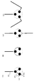
- a linear conductive member that connects each of the plurality of first electrodes to any other first electrode with a line segment may be provided.
- the line segment may be a straight line.
- the linear conductive member may be formed in a path that makes the total extension of the line segment the shortest.
- the one or more indicator electrodes connected to the plurality of first electrodes by a linear conductive member, the one or more indicator electrodes or the one or more indicator electrodes
- the device is connected to the panel by the first electrode connected to the indicator electrode at the location where the contact operation is received.
- a conductive pattern that allows the panel to detect the corresponding position may be formed in a state where the panel is in contact with or close to the surface.
- the one or more indicator electrodes are a plurality of indicator electrodes connected to each other by one indicator electrode or the linear conductive member, and are closest to the one or more indicator electrodes.
- the plurality of first electrodes may be connected.
- the one or more indicator electrodes and the plurality of first electrodes may be connected by a plurality of paths by the linear conductive member.
- the plurality of first electrodes are connected by a one-stroke path by the linear conductive member, and the one or more indicator electrodes are connected to each other at both ends connected by the one-stroke path.
- One electrode and the linear conductive member may be connected.
- the plurality of first electrodes are connected by a loop-shaped path by the linear conductive member, and at least one of the first electrodes is the linear conductive member. It may be connected with a sex member.
- all of the plurality of first electrodes may be arranged inside a rectangle having a diagonal line connecting the two most distant first electrodes.
- At least a part of the plurality of first electrodes is formed by a conductive line wired so as to form a linear pattern, and the region where at least the plurality of first electrodes are formed is the panel.
- a conductive pattern that allows the panel to detect the corresponding position may be formed in a state where the panel is in contact with or close to the surface.
- the linear conductive member may have a physical quantity in a range where the position is not detected by the panel.
- the linear conductive member formed on the first surface or another first surface is a fixed substance of ink having a volume resistivity of 1 ⁇ 10 ⁇ 5 ⁇ ⁇ cm or less.
- a conductive pattern in which the panel can detect each position may be formed in a state where at least the region where the plurality of first electrodes are formed is in contact with or close to the panel.
- the ink may be any of silver salt ink, silver nano ink, silver paste ink, and carbon ink.
- the wiring layer is formed by gravure printing or inkjet printing when using silver salt ink, flexographic printing or inkjet printing when using silver nano ink, and screen printing or inkjet printing when using silver paste ink. It may be.
- the step from the base material of the linear conductive member may be 20 ⁇ m or less.
- the line width of the linear conductive member may be 0.3 mm or less when silver salt ink, silver nano ink, or silver paste ink is used.
- the line width of the linear conductive member may be 0.15 mm or less when silver salt ink, silver nano ink, or silver paste ink is used.
- the plurality of first electrodes are connected by the linear conductive member having a predetermined length, each having a physical quantity in a range where the position is detected by the panel, and at least the A conductive pattern in which the panel can detect each position may be formed in a state where a region where the plurality of first electrodes are formed is in contact with or close to the panel.
- the panel is determined from a physical quantity generated when a finger contacts the surface opposite to the contact surface or the adjacent panel side surface of the device. The position may not be detected.
- a raised layer made of a non-conductive material that reduces a step due to the wiring layer may be formed on the first surface.
- each of the plurality of indicator electrodes includes a first indicator electrode and a second indicator electrode that are secured at a predetermined distance, the first indicator electrode serving as the first electrode, and the second indicator electrode. Is connected to the second electrode by the linear conductive member, and is laminated directly or on the first indicating electrode and the second indicating electrode by the finger to each of the first indicating electrode and the second indicating electrode.
- the first electrode includes a first electrode connected to the first indicator electrode and a second electrode connected to the second indicator electrode.
- a conductive pattern in which the panel can detect each position may be formed in a state where the region where the one electrode and the second electrode are formed is in contact with or close to the panel.
- a predetermined distance is secured between the end portions of the other second indicator electrodes adjacent to the second indicator electrode, and the second indicator electrodes are stacked directly on the plurality of indicator electrodes or on the plurality of indicator electrodes.
- the first indicator electrode may be formed so as to surround a predetermined range around the second indicator electrode.
- a gap between the first indicator electrode and the second indicator electrode formed so as to surround the predetermined range may be 1.2 mm or more.
- a gap between the first indicator electrode and the second indicator electrode formed so as to surround the predetermined range may be 1.5 mm or more.
- first indicator electrode and / or the second indicator electrode may be formed as a part of the linear conductive member.
- the indicator electrode and a part of the linear conductive member connected to the indicator electrode may be a surface opposite to the contact surface of the device or a panel side surface closer to the first surface than the first surface.
- the non-conductive substrate on the opposite surface is subjected to a contact operation with a finger, the non-conductive layer is interposed between the opposite surface and the second surface.
- a pattern may be formed.
- the indicator electrode and a part of the linear conductive member connected to the indicator electrode may be a surface opposite to the contact surface of the device or a panel-side surface closer to the first surface than the first surface.
- the second electrode on the first surface and the indicator electrode on the second surface are linear, forming a path folded at the side of the device.
- the conductive members may be connected.
- the indicator electrode may be coated with a white ink using conductive titanium oxide as a pigment, and a graphic may be printed on the coated surface.
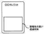
- At least a part of the apparatus may include a transparent region laminated with the one or more transparent non-conductive substrates.
- the transparent area includes one or more operation areas that are touched with a finger, and the finger is placed on at least one location of the one or more operation areas in a state of being in contact with or close to the panel.
- a conductive pattern in which the panel can detect each position may be formed according to the physical quantity including the location where the contact operation is received and the plurality of first electrodes.
- At least one linear conductive member may be formed extending in a predetermined direction from the first electrode and / or the second electrode connected by the linear conductive member.
- the physical quantity may be at least a capacitance.
- the physical quantity of the second electrode in a range where the position is not detected by the panel may be 5 pF or less.
- the function of the card can be greatly improved.
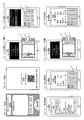
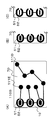
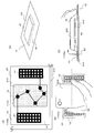
- FIG. 1 It is a figure which shows the usage example of a card type apparatus. It is a block diagram which shows the hardware structural example of an information device. It is a structural example of an apparatus. It is a structural example of an apparatus. It is a structural example of an apparatus. It is a structural example of an apparatus. It is a structural example of an apparatus. It is a structural example of an apparatus. It is a structural example of an apparatus. It is a structural example of an apparatus. It is a structural example of an apparatus. It is a structural example of an apparatus. It is a structural example of an apparatus. It is a structural example of an apparatus. It is a structural example of an apparatus. It is a structural example of an apparatus. It is a structural example of an apparatus. It is a structural example of an apparatus. It is a structural example of an apparatus. It is a structural example of an apparatus. It is a structural example of an apparatus. It is a structural example of an apparatus. It is a structural example of an apparatus. It is a structural example of
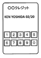
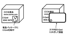
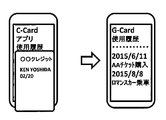
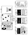
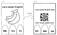
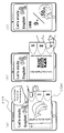
- C-Card is used as a credit card with a numeric keypad. In this embodiment, C-Card is used as a credit card with a transparent area. This is an embodiment (1) in which C-Card is used as a quality assurance card. This is an embodiment (2) in which C-Card is used as a quality assurance card. In this embodiment, C-Card is attached to a product package. It is a figure explaining the case where C-Card is used for authentication of a ticket and a coupon.
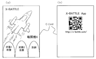
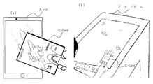
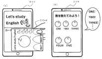
- C-Card is used as a game card. It is a figure explaining the state which is playing the game using the card for games.
- C-Card is used as an authentication card.
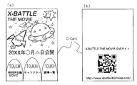
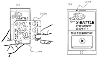
- C-Card is used as a movie card.
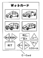
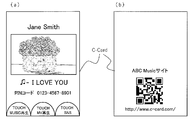
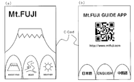
- C-Card is used as a Web card.
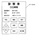
- C-Card is used as an examination ticket.
- C-Card is used as a shopping card.
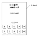
- C-Card is used as a bank ATM card.
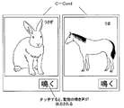
- C-Card is used as an animal card.
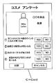
- C-Card is used as a questionnaire card.
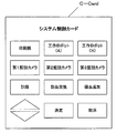
- C-Card is used as a system control card.
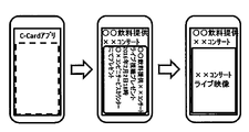
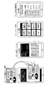
- FIG. 3 is a diagram illustrating a case where a C-Card is used for viewing music / video content, and is a diagram illustrating a C-Card for music / video content. It is a figure shown about the case where C-Card is used for viewing of music and video contents, and is a figure explaining the use state of a card. It is the figure shown about the concrete of the game card by C-Card, Comprising: It is the figure which showed the game card. It is the figure which showed about the concrete of the game card by C-Card, Comprising: It is a figure explaining the use condition of a card
- FIG.120 (b) a card is again It is a figure explaining the case where is used. It is the figure shown about the specific example of the tourist information card by C-Card, Comprising: It is the figure which showed the tourist information card. It is the figure shown about the specific example of the tourist information card by C-Card, Comprising: It is a figure explaining the use condition of a card
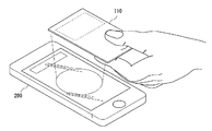
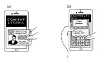
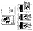
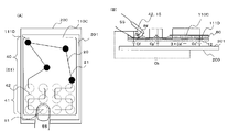
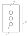
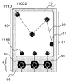
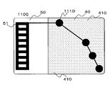
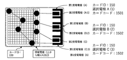
- FIG. 1 shows a usage example of the card type device 110.
- the card-type device 110 has a configuration in which conductive electrodes are embedded in a plate member made of plastic or paper.
- the card-type device 110 is used in contact with a touch panel of an information device 200 such as a mobile phone, a smart phone, a portable information terminal, a tablet terminal personal computer, or an on-vehicle device.
- an information device 200 such as a mobile phone, a smart phone, a portable information terminal, a tablet terminal personal computer, or an on-vehicle device.
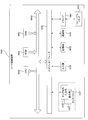
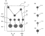
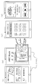
- FIG. 2 is a block diagram illustrating a hardware configuration example of the information device 200.
- the information device 200 includes a CPU 1051, a ROM (Read Only Memory) 1052, a RAM (Random Access Memory) 1053, a bus 1054, an input / output interface 1055, a touch operation input unit 1056, a display unit 1057, and an input unit. 1058, a storage unit 1059, a communication unit 1060, and a drive 1061.
- the CPU 1051 executes various processes according to a program recorded in the ROM 1052 or a program loaded from the storage unit 1059 to the RAM 1053.
- the RAM 1053 appropriately stores data necessary for the CPU 1051 to execute various processes.
- the CPU 1051, the ROM 1052, and the RAM 1053 are connected to each other via a bus 1054.
- An input / output interface 1055 is also connected to the bus 1054.
- a touch operation input unit 1056, a display unit 1057, an input unit 1058, a storage unit 1059, a communication unit 1060, and a drive 1061 are connected to the input / output interface 1055.
- the touch operation input unit 1056 includes, for example, a capacitance type position input sensor stacked on the display surface of the display unit 1057, and detects the coordinates of the position where the touch operation is performed.
- the touch operation refers to an operation of touching or approaching an object with respect to the touch operation input unit 1056.
- An object in contact with or close to the touch operation input unit 1056 is generally a user's finger or a touch pen.
- touch position the position where the touch operation is performed
- touch coordinates the coordinates of the touch position
- the display unit 1057 is configured by a display such as a liquid crystal and displays various images.
- the touch operation input unit 1056 and the display unit 1057 constitute the touch panel 1031 described above.
- the input unit 1058 is composed of various hardware buttons and the like, and inputs various information according to the player's instruction operation.
- the storage unit 1059 is configured by a DRAM (Dynamic Random Access Memory) or the like, and stores various data.
- DRAM Dynamic Random Access Memory
- the communication unit 1060 controls communication performed with other devices via the network N including the Internet.
- the drive 1061 is provided as necessary.
- a removable medium 1071 including a magnetic disk, an optical disk, a magneto-optical disk, a semi-electrode memory, or the like is appropriately attached to the drive 1061.
- the program read from the removable medium 71 by the drive 1061 is installed in the storage unit 59 as necessary.
- the removable medium 1071 can also store various data stored in the storage unit 1059 in the same manner as the storage unit 1059.
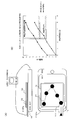
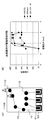
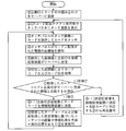
- ⁇ Embodiment 2> [Regarding the threshold value of touch panel electrodes] (1) Threshold change when 10 seconds elapse on smartphones For many iPhone (registered trademark) models, depending on the detected capacity, the conditions for issuing touch status events may be the first and second thresholds (other than that, there may be error handling settings for each electrode). There is. At the moment when an electrode such as the electrode 111 of the device 110 touches the touch panel, the first low threshold is used, and the touch panel has an ON threshold for detecting (ON) the electrode even with a relatively low capacity.
- the OFF threshold is set so that it is turned OFF with a lower capacity than when ON is detected so that it does not become undetected (OFF) due to a slight change in the detected capacity due to hysteresis.
- the second threshold value is set for all the electrodes. At that moment, if the detection capacity of the electrode is lower than the second threshold OFF capacity, the touch panel immediately detects no electrode. However, while all the electrodes are moving, it is assumed that the finger is moving, and the first threshold is continuously applied.
- the presence of the electrode is always detected even if it is not detected as long as there is a certain capacity, and when the electrode moves, the touch panel follows the movement And the electrode is detected.
- an event including error setting
- various developed applications recognize the state of electrode detection (including error setting).
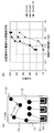
- the detected capacitance is further reduced due to the characteristics of the touch panel, and one or all of the arranged electrodes are There is a case where it becomes OFF.
- electrodes that are not detected in the horizontal or vertical state are detected by the touch panel when moved so as not to be aligned horizontally or vertically. To avoid this, it is desirable to increase the capacitance of the electrode so that a sufficient capacitance is detected. Even if it is a person's finger, when the child's finger or the contact surface is small, the capacity is insufficient, and therefore it is not detected when the second threshold is applied. Thereafter, when the contact area is increased, the capacity is increased, and the electrode is moved, detection is performed again, but the behavior of the touch panel becomes unstable (it is estimated that an error has been set).
- the capacitance to be detected is more easily detected if the electrode area is large, the degree of adhesion to the screen is high, and the capacitance of the electrode including the linear conductive member is large.
- many current smartphones detect up to 5 electrodes, but if 5 are exceeded, an error event is issued and all electrodes are set to error.
- an error event does not occur in a conductor such as an elongated finger, but an error event is issued in a massive conductor such as a fist.
- a smartphone determines that it is not a human finger that is processed as an error. Even if the capacitance threshold is not exceeded, if the capacitance is detected over a wide range, the electrodes that have been detected may not be detected even if no error event is issued.
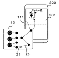
- the touch area of this embodiment is not provided with a through hole (conduction hole) or electrode in order to be manufactured at a low cost. Touch can be detected simply by providing a dielectric column.
- the detection capacity of the electrode in the ID area is small, and if it is used on a wooden desk (the detection capacity is small compared to steel attachment), it will not be detected in 10 seconds. In some cases. Needless to say, the capacitance detected by the touch panel is easier to detect if the electrode area is large, the electrode capacitance including the linear conductive member is large, and the degree of adhesion with the touch panel is high.
- the electrodes can be detected normally if the second threshold value is sufficient for all the electrodes to detect, and can be in a stationary and / or moving state for 10 seconds or more. Not limited, continue to detect normally. Many current smartphones detect up to 11 electrodes, but if 11 are exceeded, an error event is issued and all electrodes are set to error.
- the conductive column may be fitted into the bottom plate, or may be provided on the bottom plate by multiple molding. Further, this conductive column may be a metal rod or a metal wire. Note that from 2), 1) is more capable of detecting a large capacity and reacting more easily because a circuit between the touching human body and the touch panel can be formed via the housing of the smartphone.
- a linear conductive member longer than 25cm in length is provided to detect the four electrodes in the ID area while holding the capacitance without touching with a finger.
- the touch panel can detect the electrode.
- the length of the linear conductive member, the size of the contact and the tap so that the touch panel can reliably detect the capacitance of all the electrodes in the ID area simply by placing the device 110 on the touch panel without touching the member.
- the touch panel can detect the electrode in the ID area even if it exceeds 10 seconds in many operation tests in 1). However, it is desirable to use a mechanism for wiring to the touch area and conducting to the electrode in the ID area (AC signal can be conducted) so that the electrode can be detected again.
- AC signal can be conducted
- the screen of the smartphone since the screen of the smartphone is small, after placing the card and touching one touch area, remove the card from the screen to view the app execution and content, after placing the card It is considered that the use condition of touching the touch area within 10 seconds may be acceptable. If the card-like device 110 is placed and the touch panel reliably detects the four electrodes in the ID area even once, there is no need for conduction from the finger to the electrodes in the ID area via the wiring.
- the ID area can be separated.
- the touch panel can detect the four electrodes in the ID area.
- the smartphone can detect the subsequent touch on the touch area without misrecognition for more than 10 seconds.
- the tablet has a better touch detection response of the electrode than the smartphone, and can be detected continuously. It is not necessary to provide a through hole (conduction hole) and an electrode in the touch area. However, it is difficult for the touch panel to detect the capacitance of the electrode depending on the conditions such that the material of the dielectric pillar is low, the diameter of the dielectric pillar is less than 8 mm, the thickness of the card is 0.8 mm or more. In addition, the manufacturing cost can be reduced at a low cost if no through hole (conduction hole) or electrode is provided.
- a capacitance is provided by providing a linear conductive member longer than 25 cm in order to detect the four electrodes in the ID area while retaining the capacitance. It connects with an electrode by the through hole (conduction hole) provided above. Because the case is large and the stray capacitance between the ground and the human body to be operated is large, a large amount of capacitance is detected, and even if the second threshold is applied over 10 seconds, detection of the electrode in the ID area can be continued, Very good.
- the detected capacity decreases due to the characteristics of the touch panel, and either one or all of the arranged electrodes are There is a case where it becomes OFF.
- a through hole (conduction hole) and an electrode are provided also in the touch area as shown in FIG. 4 of this embodiment so as to detect a sufficient capacity, the frequency of non-detection is greatly increased. descend.
- the card-like device 110 is placed on the touch panel and the four electrodes in the ID area are reliably detected even once, the finger (alternating current signal) to the electrodes in the ID area through the wiring There is no need for continuity, and the touch area and ID area can be separated.
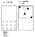
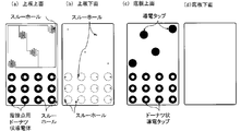
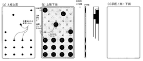
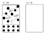
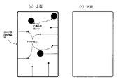
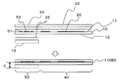
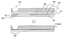
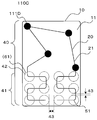
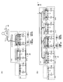
- a device 110AB according to the sixth embodiment will be described with reference to FIGS.
- the device 110AB of this embodiment is a thin plate-like device as in the first and second embodiments.
- a generic term for such a card-type device is also referred to as “C-Card”.
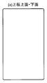
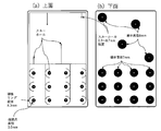
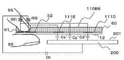
- the surface that is close to or in contact with the touch panel among the surfaces of the thin plate viewed in plan is called an action surface. Further, the surface opposite to the working surface is referred to as the upper surface.
- Both the action surface and the upper surface of the device 110AB have the same ID region and touch region as those of the first embodiment, the second embodiment, and the like.
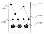
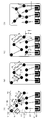
- the electrode 111 in the ID area and the touch point in the touch area are referred to as electrodes, and the planar shape formed by the shape and arrangement of the electrode 111 in the ID area and the touch points in the touch area is referred to as a conductive pattern.
- a mold is produced for each electrode pattern including the electrode 111 in the ID area and the touch point in the touch area in order to arrange many patterns in the ID area. Design, construction methods, and materials are used so that they do not have to be.
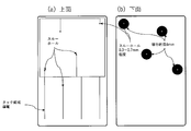
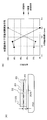
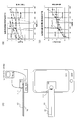
- the upper plate is a highly non-conductive sheet or molded plate so as not to bend when bonded. For this purpose, a material that is hard or does not stretch is used.
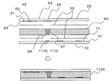
- the contact surface between the touch panel and the card is preferably made of a material that can hold a flat surface, and it is desirable to mold the bottom plate of FIGS.
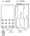
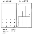
- the upper plate and the bottom plate above the center of the candidate portion where the electrodes are arranged on the bottom plate are provided. It is desirable to provide a hole for the through hole TH1 that connects the electrode and the wiring. These holes may be formed at the time of molding, or holes may be formed at necessary places after molding.
- the through-holes need to have a diameter of about 0.3 to 1.0 mm. On the other hand, depending on the mechanism, there is a case where it is not necessary to make a hole in the upper plate as shown in FIGS.
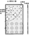
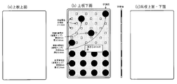
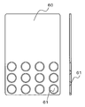
- holes for through holes TH2 are provided at 12 locations in the touch area of the bottom plate.
- the front and back of the card can be printed directly because the upper plate has a thickness of 0.2 to 0.3 mm and can be handled by various printing machines. Since the bottom plate is thick, it is desirable to separately print it on a white sheet and attach it to the back surface of the bottom plate. In addition, when it is necessary to blind the electrode 111, the wiring, and the contact, it is desirable to blind the white sheet (other colors may be used depending on the graphic) and print the graphic thereon to produce a printed sheet.
- the printed sheet including the ink layer and the adhesive layer should be within 0.1 to 0.15 mm so as not to affect the detection of the electrode 111.
- the thickness of the printed sheet is preferably within 0.005 to 0.015 mm including the adhesive layer in order to enable conduction from the finger.
- Directly printing on the upper plate has the highest conductivity.
- the electrode 111 is also referred to as an electrode or simply a tap.
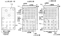
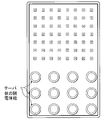
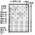
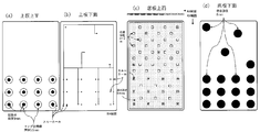
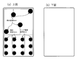
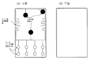
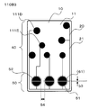
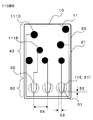
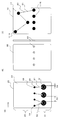
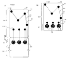
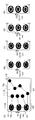
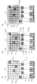
- the thickness of the bottom plate in FIGS. 3B and 3C is, for example, 0.6 mm to 0.8 mm, and through holes for arranging 56 electrodes of 7 rows in the horizontal direction and 8 rows in the vertical direction in the ID region.
- Columns for holes 2 mm ⁇ 2 mm are provided at intervals of 6 mm (ID region columns). The dimensions and number of these columns are design conditions, and the number of electrodes (electrodes 111) connected to the wiring via the columns and through holes is arbitrary.
- the interval of 6 mm is highly likely to be detected when the finger touches a position other than the electrodes to be arranged, but is set to an interval of 6 mm in order to increase the number of electrode arrangement candidates.
- This groove will provide an air layer with the lowest dielectric constant (1), so that the touch panel will not misidentify the touch by finger touch or the wiring / contact of the upper plate as a physical quantity change from the device 110AB, This is for correctly detecting only the electrodes.
- the column may be circular or polygonal, but it is desirable that the cross-sectional dimension be as small as possible. This is because when the upper plate is touched with a finger, the touch panel may detect the capacity of the finger through the column if the size of the column is large.
- a conductive pattern array of the electrodes 111
- the ID area is detected by touching a position other than the arrangement with a finger, the ID area defined by the electrode pattern is misidentified. Because it occurs.
- detection of an electrode at an impossible position is recognized as an error in pattern recognition on the touch panel side, but every time the card is touched with a finger, an error frequently occurs and the operation cannot be performed normally. Therefore, it is desirable that the through-hole column is as small as possible, and is within 2 ⁇ 2 mm when the cross-sectional shape is rectangular, and within 3 mm when the cross-sectional shape is circular.
- the touch panel may detect the capacitance as one electrode through a plurality of columns when touched with a finger, and at least the interval between the column ends. It is desirable to set a distance of 4 to 6 mm or more. The size of the distance is greatly influenced by the thickness of the top plate, the gap (groove depth) of the bottom plate, and the characteristics of the dielectric constant of the bottom plate.
- the thickness of the bottom plate is 0.2 to 0.3 mm, and this thickness can be molded with a non-conductive hard thermosetting resin for maintaining the flatness of the bottom surface of the card.
- a pillar In the touch area, a pillar (touch area pillar) is arranged on the bottom surface for through-hole TH2 for arranging 12 electrodes in 4 rows in the horizontal direction and 3 rows in the vertical direction and for preventing the card from bending. Are provided at intervals of 14 mm in the horizontal direction and 12 mm in the vertical direction. This pillar is also called a touchpoint pillar.
- the cross section is circular in FIG. 3 (b), and the diameter is preferably about 3 mm to 8 mm.
- the diameter of the column cross section may be about 3 mm as in the ID region, but when the through hole is not provided, the diameter of the column cross section is preferably about 8 mm so that the finger capacity can be detected.
- the column shape is rectangular, and the cross-sectional dimension is preferably about 2 ⁇ 2 mm to 7 ⁇ 7 mm.
- the dimension of the column cross section may be about 2 ⁇ 2 mm as in the ID region.
- the dimension of the column cross section is about 7 ⁇ 7 mm so that the finger capacity can be detected. desirable.
- the area other than the touch point is provided with a groove having a depth of 0.4 to 0.5 mm as in the ID area, and its function is the same as that of the ID area.
- the use of a pillar without a through hole includes a method in which the lower electrode is not used, so that the insufficient capacity makes effective use of coupling by finger contacts and wiring arranged on the upper plate. .
- ⁇ To hide the wiring and finger contacts on the card surface paste a sheet of white (other colors may be used depending on the graphic) that can print the graphic.
- the white sheet is preferably within 0.005 to 0.015 mm including the heel adhesive layer in order to allow conduction from the finger.
- the obstacle is that the user's finger touches the finger contacts of the adjacent touch points at the same time, and the touch panel detects the electrodes of the two touch areas.
- the electrodes are arranged at a sufficient interval (for example, a length of 12 mm and a width of 14 mm), and are designed so that they cannot be touched at the same time.
- the electrode in the touch area is energized through the through hole, and the touched position can be detected reliably.
- the ring-shaped conductor and the finger contact should be separated by about 1 mm or more so that they do not conduct between the two. It is desirable to make it.
- a ring-shaped conductor and a circular finger contact are shown. However, if there is no conduction between the conductor for conduction to the ID area and the finger contact for the electrode, any shape such as an ellipse, a polygon, etc. Various shapes and combinations may be used.
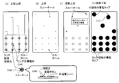
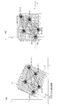
- a ring-shaped conductor 114C for example, a diameter of 6 mm
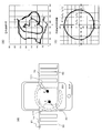
- an indicator electrode finger contact, rectangular ridge 1.0 x 1.0 to 2.0 x 2.0 or about 1.5 to 3 mm in diameter
- the electrode 111 arranged immediately below in FIG. 4D conduction is made to the electrode 111 arranged immediately below in FIG. 4D through the finger contacts and through holes in FIG. 4B and FIG.
- the four electrodes 111 arranged in the ID area are conducted, and a total of five electrodes 111 are detected by the touch panel.
- the extension of the linear conductive member is 25 cm or more with only the linear conductive member with a fixed touch area, and has a capacity greater than the threshold value detected by the touch panel, iPhone (registered trademark) and iPad (registered trademark). However, it has been confirmed that the four electrodes in the ID area can be detected simply by placing the device 110AB on the touch panel.
- the linear conductive member having a length of 20 cm or more is interdigital, but it may have any shape such as a lattice or a spiral.
- the threshold of the physical quantity (for example, capacitance) detected by the touch panel changes after 10 seconds have passed since the operation such as placement on the touch panel by the device 110AB. Although it is not detected, it has been confirmed that the tablet can continue to detect the electrode for an unlimited time. Therefore, in the following, the threshold when the touch panel determines the presence or absence of physical quantity detection immediately after performing an operation such as placing the device 110AB on the touch panel of the smartphone is referred to as a first threshold. In addition, a threshold that is set when about 10 seconds have elapsed from this operation is referred to as a second threshold. It has been confirmed that the second threshold is higher than the first threshold.
- a through hole of 0.3 to 1.0 mm is formed in the upper plate of FIG. 4B, and the user's finger is conducted to the electrode 111 by the finger contact or the finger touch on the ring electrode 114C.
- a through hole is provided in a column having a height of 0.4 to 0.5 mm on the upper surface of the bottom plate, and an ID arranged on the lower surface of the bottom plate as shown in FIG. 4 (d). Conducted to the four electrodes in the region.
- electrodes are arranged at intervals of 12 mm in length and 14 mm in width, and each of the electrodes has a diameter of about 8 mm.
- An electrode having a diameter of 8 mm generally corresponds to a finger touch area (maximum length in contact).
- the finger contact has a slightly horizontally long aspect ratio because the contact area is slightly horizontally long when a human finger comes into contact with the finger contact. This prevents the adjacent finger contacts from being touched simultaneously.
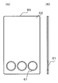
- Different icons are printed on each of the 12 touch areas. When one of the touch areas is touched, one electrode is detected in addition to the four electrodes in the heel ID area, and is printed on the device 110AB. The application identified by the icon related to the identified image can be executed or the content identified by the icon can be browsed.
- a rectangular 1.0 x 1.0 to the contact point of the through hole on the top plate and the through hole on the bottom plate It is desirable to provide a junction contact having a diameter of about 2.0 ⁇ 2.0 or a diameter of about 1.5 to 3 mm.
- a button having a diameter of about 6 to 10 mm and a rectangle of about 5 ⁇ 5 mm to 8 ⁇ 8 mm molded with a conductive material on which an icon is printed may be arranged at the center portion (each touch point) of the 12 touch areas. Adjacent buttons may be kept away from each other with an interval of 1 mm or more. However, if the area of the conductive button is too large, the range of the capacitance that is detected due to coupling becomes excessive, and an error occurs or the touched position does not match the detected position, so the button size is You need to be careful. You may control by the electroconductivity of the electrically-conductive material used for a button.
- the twelve conductive buttons are preferably arranged on a sheet formed of a non-conductive material.
- the lower part of the conductive button of the sheet must be pierced to allow conduction.
- the conductive button and the nonconductive sheet may be integrally formed by multiple molding.
- the button and the seat are integrally molded with a material having a relatively weak appropriate conductivity. Also good.
- guide light may be emitted from a touch panel to a predetermined touch area in order to guide touch in each touch area for games and security.
- the guide column at the lower part of the touch area may be made translucent, or a hollow part may be provided in the guide column.
- the electrode may be formed in a donut shape.
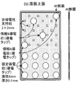
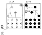
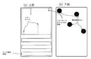
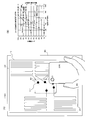
- FIGS. 6 to 9 show that high-quality graphics are directly printed in areas other than the touch area, and when high-quality printed sheets are affixed to the card, conductors and through-holes can be seen through.
- nothing is provided on the upper surface of the upper plate and wiring and contacts are provided on the lower surface so as not to cause unevenness.
- wiring and / or conductors are arranged on both the upper surface and the lower surface of the upper plate, which increases the cost.
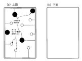
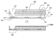
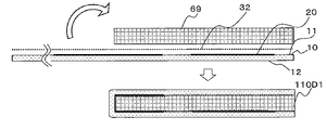
- FIG. 6 shows an embodiment in which the ID region wiring is wired on the lower surface of the upper plate.
- the ID region on the upper surface of the upper plate is not provided with a mechanism that conducts by finger touch.
- the electrode 111 on the bottom surface of the bottom plate in the touch area only needs to be brought into conduction with the top surface of the upper plate by finger touch. Therefore, it is desirable to provide a finger contact that is as inconspicuous as possible.
- the ID region since there is no conduction from the finger in the ID region, the ID region has a capacity with wiring (including a coupling conductor) and electrodes. However, if the card is deformed, the surface of the touch panel is attached with small dust or the like, or the protective sheet is not attached well, the electrode may not be recognized and attention is required.
- FIG. 7 and 8 show an embodiment in which the wiring on the upper surface of the upper plate of the ID region in FIG. 4 is wired on the lower surface of the upper plate.
- This is also a mechanism for forming a high-quality graphic in an area other than the touch area.
- the difference from FIG. 6 is that the ring-shaped conductor 114C on the upper surface of the upper plate is connected to the wiring WR on the lower surface of the upper plate and the electrode in the ID region of the lower surface of the bottom plate through the conductive member in the through hole. Therefore, since the user is conducted to the electrode in the ID area by finger touch on the conductor 114C, the contact state between the card and the touch panel, and the mechanism that can detect the capacity reliably even if the detection capacity of the touch panel is somewhat low, It has become.
- a ring that surrounds the finger contact 114A and its periphery in the center of each touch area on the upper plate surface so that the touch area does not stand out even if graphics are printed on the upper surface or a printed sheet is pasted 114C is provided, and a conductive path passing through the through hole is provided on the ring-shaped conductor 114C and connected to the wiring WR on the lower surface.
- a through hole is provided so as to conduct from the finger contact 114A to the electrode immediately below, and a conductive path is formed in the through hole.
- the card surface may be printed with a design such that the finger contacts 114A and the ring-shaped conductor 114C are not conspicuous at 12 locations in each touch area.
- the finger contacts 114A and the ring-shaped conductor 114C may be exposed or printed with similar color graphics.
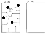
- FIG. 9 shows a mechanism in which guide light is emitted from a touch panel to a predetermined touch area so that the user can visually recognize the touch in each touch area for games and security.
- the finger contact is a donut-shaped conductor, and a through-hole is provided in this conductor, but a ring-shaped conductor as shown in FIG. 6A may be used.
- the guide column (touch region column) on the bottom surface of the bottom plate of the touch region in FIG. 9C is made translucent, or a hollow portion is provided in the guide column so that light can be transmitted and visually recognized.
- the electrode may be formed in a donut shape as shown in FIG.
- the wiring in which the electrodes in the ID area cannot be conducted by finger touching may be used.
- FIGS. 3 to 8 can also be designed so that the guide light can be visually recognized, such as a donut-shaped electrode or a conductor for conducting to the electrode in the ID region.
- the touch position can be indicated by the guide light even if there is no icon printing on the card surface.
- the guide light may selectively guide a finger touch with light emission of different colors. Further, the finger touch may be selectively guided by changing the blinking interval (light emission / light-out time). The set light and light other than the set light may be emitted simultaneously. Multiple touches may be made at the same time.
- the position to be touched next may be instructed, or the item selection, character movement, attack direction, language, etc. may be determined by the emission color or flashing light.
- the user sets the emission color and blinking, and as a one-time password, various lights are emitted with time changes in some or all touch areas, and the preset light is selected and You can enter a one-time password by touching the touch area.
- a plurality of light colors and blinking orders are set including the order of touching, higher security can be realized.
- the set light position is not touched and the left, right, up, down, and diagonal directions of the position are touched, skimming is not easily performed.
- the molding material of the card is made transparent, an image can be displayed outside the touch area. Accordingly, it can be used for switching images by touching with a finger and ordering / settlement of the image (product or service).
- an image can be displayed in the touch area and switched freely.
- FIGS. 4 to 9 are described as specific examples to which the structure of FIG. 3 is applied, but how these various conductive wirings, conductors, through holes, contacts, and electrodes are combined, You may form in the mechanism of FIG.
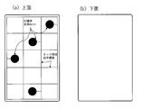
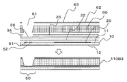
- the device 110AC according to the fourth embodiment will be described with reference to FIGS.
- the device 110AC of the present embodiment is a thin plate-like device as in the first to sixth embodiments. Both the operation surface and the upper surface of the device 110AC have the same ID region and touch region as those in the first to sixth embodiments.
- the structure of the upper plate and the bottom plate of the device 110AC is opposite to that of the sixth embodiment.
- Other configurations and operations of the present embodiment are the same as those of the sixth embodiment.
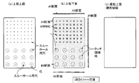
- the device 110AC is formed of two pieces, an upper plate and a bottom plate, and uses a design, a construction method, and a material so that it is not necessary to manufacture a mold for each electrode pattern in order to arrange many patterns in the ID region. .
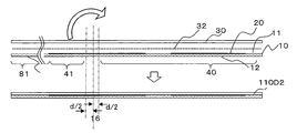
- the thin upper plate of FIGS. 3 (a) and 3 (b) is used as the bottom plate of FIGS. 10 (c) and 10 (d), and the uneven bottom plate of FIGS. It is the Example used as the upper board of a) and (b).
- This embodiment has two types of features, one of which is that the ID region and the touch region electrode 111 are formed on the upper surface of the bottom plate, and the electrode is not formed on the lower surface of the bottom plate in contact with the touch panel surface.
- a good mechanism can be realized.
- an electrode is formed on the bottom surface of the bottom plate, a slight level difference is generated on the bottom surface.
- an air layer is formed between the lower surface of the bottom plate that is the working surface and the touch panel, and the detection accuracy of physical quantities such as capacity by the touch panel decreases. To do.
- the thin bottom plate can be molded with a hard material and the flatness can be maintained, the card and the touch panel surface are in close contact with each other, the generation of an air layer is suppressed, and the touch panel can easily detect the capacitance of the electrode on the upper surface side of the bottom plate.
- the distance from the electrode instead of the finger to the touch panel surface is about 0.2 to 0.3 mm of the thickness of the bottom plate, and the thickness of a general protective sheet covering a touch panel such as a smartphone is around 0.5 mm. There is no significant effect on electrode detection.
- the second feature is that if the color of the bottom plate is molded in white (other colors may be used depending on the design), the thickness of the bottom plate is 0.2 to 0.3 mm, so printing with various printing machines is possible.
- the back side graphic can be easily printed.
- the electrode on the upper surface of the bottom plate can be printed with conductive ink.
- the bottom plate is a highly non-conductive sheet or molded plate so as not to bend when bonded.
- a material that is hard or / and does not stretch is used.
- the contact surface between the touch panel and the card is preferably made of a material that can hold a flat surface, and the bottom plate is preferably molded.
- FIGS. 10 (a) and 10 (b) it is necessary to provide a through hole for connecting the electrode and the wiring at a candidate position where the electrode is arranged on the upper surface of the bottom plate.
- These holes may be formed at the time of molding, or holes may be formed at necessary places after molding.
- the through-holes need to have a diameter of about 0.3 to 1.0 mm.
- through-holes are provided at 12 locations on the touch area of the upper plate.
- the upper plate is molded with a plate of about 40 cm ⁇ 50 cm or more, wiring is performed by printing or plating with a conductive ink, and after bonding, the through hole is filled with the conductive ink.
- a contact is provided so that the through hole of the upper plate is connected to the electrode of the bottom plate.
- the upper plate Since the upper plate is thick, it is desirable to print the card surface separately on a white sheet and attach it to the upper plate surface. When it is necessary to blind the electrodes, wirings, and contacts, it is desirable to blind them with a white sheet (other colors may be used depending on the graphic) and print the graphic thereon to produce a printed sheet.
- the white sheet should be within 0.1 to 0.15 mm so as not to affect the detection of the electrode.
- the thickness of the printed sheet is preferably within 0.005 to 0.015 mm. In the manufacturing process, considering the cost, wiring, contacts, through-holes, electrodes, etc. are formed on the top and bottom plates, and printing or printing sheet bonding is performed in the proper order. After pasting, it is desirable to cut the card size.
- a groove having a depth of 0.4 to 0.5 is formed in a region other than the pillar on the lower surface of the upper plate. Therefore, basically, the conductive wiring for the electrodes in the ID region and the conductor for finger contacts in the touch region are formed on the upper surface of the upper plate.
- the conductive wiring on the upper and lower surfaces of the upper plate is the same as that shown in FIGS. 4A and 4B.
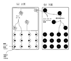
- 11C and 11D four electrodes are formed on the ID region of the bottom plate, and twelve electrodes are formed on the touch region.
- a sheet of white other colors may be used depending on the graphic
- the manufacturing process is performed by pasting the top plate and the bottom plate after printing or after pasting the printed sheet. The same applies to FIG. 12 shown below.
- FIG. 12 (a) and 12 (b) is provided with a doughnut-shaped conductor for finger contact on the upper surface of the touch area, and has a predetermined area so that the finger touch can be conducted even if a blindfold sheet is applied. is doing. Further, in the touch area on the upper surface of the bottom plate in FIG. 12C, a donut-shaped electrode having the same size as the conductor of the upper plate is provided so that the guide light from the touch panel can be transmitted and visually recognized. 11 to 12 have been described as specific examples to which FIG. 10 is applied. However, the various conductive wirings, conductors, through holes, and electrodes in FIGS. 4 to 9 and 10 to 19 can be selected. These mechanisms may be combined to form the mechanism of FIG.
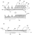
- the dielectric pillars provided on the upper plate of the present embodiment and the bottom plate of the sixth embodiment may be tapered.
- FIG. 13 illustrates a thin plate-like substrate having a tapered dielectric.
- the base material of FIG. 13 is used for the bottom plate of the sixth embodiment or the upper plate of the seventh embodiment. For example, when the devices 110AB, 110AC, etc.
- the touch panel increases the physical quantity detected on the working surfaces of the devices 110AB and 110C, and widens the touch point spacing on the upper plate upper surface (opposite surface of the working surface) of the devices 110AB and 110AC. It is possible to take. By making the distance between the touch points wide, it is possible to avoid interference with the finger touch between the touch points.
- the side close to the touch panel of the dielectric pillar may be thin, and the surface far from the touch panel surface may be thick.
- the ID region is provided with a large number of ID region pillars with through holes.
- the through holes are formed.
- the devices 110AB, 110AC, etc. before forming the electrode 111 (or their top and bottom plates) Can be mass-produced. That is, for example, a large number of bottom plates as shown in FIGS.
- 3B and 3C (or an upper plate as shown in FIG. 10B) are produced with the same mold, etc.
- the electrode 111 is an example of a plurality of first electrodes and second electrodes formed on the first surface.
- the wiring is an example of a linear conductive member.
- a through hole is an example of a hole.
- FIGS. 14 to 19 A method for manufacturing the device 110 is illustrated with reference to FIGS. 14 to 19, the device 110 is formed of two sheets, an upper plate and a bottom plate, and the bottom plate is formed by multiple molding using a conductive material and a non-conductive material. Twelve fixed conductive columns, two information A conductive columns, and two information B conductive columns are formed of a conductive material. The twelve fixed conductive columns are a mechanism that allows the capacitance to be detected only at the bottom of the fixed conductive columns so that even if a finger touches in the touch area, even if the position deviated from the fixed conductive columns is touched. Yes.
- the two information A conductive columns are arranged at fixed positions, but the two information B conductive columns are arranged at arbitrary positions, thereby forming a conductive pattern of the ID region.
- the two information A conductive columns may also be arranged at arbitrary positions.
- the structure of the mold allows the conductive pillar and the non-conductive support pillar to be arranged at a required position.
- the support pillars are arranged at predetermined intervals so as not to bend when the thin upper plate is pressed with a finger.
- the size of the support columns is preferably about 2 ⁇ 2 mm or less for a rectangle, and about 3 mm or less for a circle, and at least the interval between the column end portions is preferably 4 to 6 mm or more.
- the upper plate of FIG. 14 is provided with a finger contact on the upper surface and a contact with a conductive column on the lower surface.
- the conductive wire is formed on the upper surface and / or the lower surface.
- a through hole is provided in the upper plate, but it is not necessary to provide a through hole on the bottom surface by arranging conductive columns.
- normal molding may be performed with a non-conductive material, and conductive columns may be arranged from the upper surface of the bottom plate and the lower surface may be bonded.
- FIGS. 4A and 4B and FIGS. 25 to 32 can be applied.
- 6A and 6B can be applied without forming a conductor on the lower surface. Otherwise, FIGS. 11A and 11B can be applied.
- a conductive pillar having a diameter of 8 mm is formed into a cylindrical shape (the hollow portion is a gap or a transparent non-conductive material), and guide light is emitted from the touch panel to a predetermined touch area to guide touch in each touch area. And visible from the card surface.
- normal molding may be performed with a non-conductive material, and conductive columns may be arranged from the upper surface of the bottom plate and the lower surface may be bonded. 6, 12 (a), (b) and FIGS. 29 to 77 can be applied as the upper plate of the bottom plate.
- a notch is provided in the central vertical direction of a conductive pillar having a diameter of 8 mm, and in order to guide the touch of each touch area as in FIG. 16, guide light is emitted from the touch panel to the predetermined touch area, and the card surface Visible from.
- normal molding may be performed with a non-conductive material, and conductive columns may be arranged from the upper surface of the bottom plate and the lower surface may be bonded.
- FIG. 6, FIG. 12 (a), (b), and FIG. 29 are applicable as an upper plate of this bottom plate.
- 20 and 21 are wiring diagrams of the upper plate taking advantage of the features of the notched conductive pillars of FIG.
- the ring contact wire for finger contact in FIG. 20 (a) is used as a donut shape as shown in FIG.
- the conductor may be formed.
- 20 and FIG. 21 may use the wiring shown in FIG. 8B or FIG. 12B.
- pot-shaped conductive pillars are arranged by multiple molding.
- the conductive pillar has a lower diameter of 8 mm, a thickness of 0.3 mm, an upper diameter of 3 mm, and a thickness of 0.4 mm.
- the lower portion of the conductor is flush with the bottom surface of the bottom plate, so that the capacitance can be detected reliably.
- normal molding may be performed with a non-conductor, and the non-conductor may be fitted from the upper surface of the bottom plate and bonded around the lower portion of the conductive column.
- the blindfold sheet is covered.
- FIGS. 4A, 4B, 7, 8, and 25 to 32 can be applied. In addition, it is applicable even if there is no wavy wiring on the lower surface of the upper plate in FIG.
- the conductive pillars used in FIGS. 15 to 23 are not limited to conductive molded products, but may be any material as long as it has a high conductivity, and may be a metal.
- the conductive wiring 22B are formed with a thickness of 0.4 mm and a diameter of 8 mm below the upper surface of the bottom plate having a thickness of 0.3 mm, in principle, the conductive wiring is formed on the upper plate. It must be formed on the top surface and have a through hole in the conductive column in the ID region to make it conductive. In that case, a blindfold sheet is required.
- the blindfold sheet is printed with a graphic, but it is preferably within 0.005 to 0.015 mm including the adhesive layer in order to conduct the ID region electrode from the finger.
- the bottom plate is a white plate (or other color) 0.2 mm thick plate or sheet in FIG. In addition, the lower surface of the bottom plate can be printed directly.
- the bottom plate is made of a highly dielectric non-conductive sheet (including paper, PET, etc.) or a molded plate, but it needs to hold a flat surface so that it touches the touch panel. Do not.
- a material that is hard or does not stretch is used.
- normal molding may be performed with a non-conductive material, and conductive columns may be arranged and bonded from the upper surface of the upper plate.
- the wiring on the upper surface of the upper plate the wiring on the upper surface, finger contacts, and through holes in FIGS. 4, 11, and 25 to 31 can be applied.
- This upper plate is an appropriate mechanism in which normal molding is performed with a non-conductive material in addition to multiple molding, and a conductive column is fitted and bonded to the upper surface of the bottom plate.
- a blindfold sheet is necessary.
- the blindfold sheet is printed with a graphic, but it is preferably within 0.005 to 0.015 mm including the adhesive layer in order to conduct the ID region electrode from the finger. Directly printing on the upper plate has the highest conductivity.
- the conductive pillar may be anything as long as it is a highly conductive material in addition to a conductive molded product, and may be a metal.
- electrodes formed by printing with metal, plating, conductive ink, and conductive pillars molded with a conductive material that doubles as an electrode and a through hole Combinations of finger contacts that conduct when touched, contacts that conduct two conductive parts, and through holes that penetrate the plate and conduct in the thickness direction, as long as they retain their original functions May be used. Further, if wiring and graphics cannot be formed directly on the flat surface side of the concavo-convex plate, another sheet may be provided to form wiring and graphics on the sheet.
- the wiring to the flat surface serving as the upper surface may be reduced as much as possible, and wiring may be made to the concave portion on the concavo-convex side.
- both the ID area and the touch area are provided, but either one may be used.
- a wiring requiring a sufficient capacity exceeding 25 cm is formed. To wire in a small area, you can easily earn a distance of 25cm by wiring in a wavy or spiral shape.
- the upper surface of the bottom plate has the same characteristics as those in FIG. 14, and the applicable top plate is also the same.
- FIG. 24 shows a mechanism in which the cross section of the bottom plate column in the touch region of the upper plate in FIGS. 14 to 26 is reduced to suppress the coupling of the conductors wired in the touch region.
- the manufacturing cost can be reduced. Therefore, in the C-CARD mechanism provided with the above-mentioned void layer, it is possible to significantly reduce the cost by manufacturing with a mechanism in which the air space layer is filled with a material having low non-conductivity. In that case, since no void layer is provided, the thickness can be reduced by about 0.2 to 0.4 mm, depending on the mechanism. It is also possible to use the cheapest paper. Note that the card thickness is assumed to be within about 0.6 to 0.8 mm, and it is not necessary to provide an electrode in the touch area.
- the touch position can be freely determined for each card. Furthermore, at least a part of the ID area and the touch area may be mixed. That is, the electrode in the ID area and the touch position in the touch area may be mixed.
- the front and back surfaces of the card may be either 1) directly printing or 2) pasting a graphic-printed sheet to hide the conductors, finger contacts, and electrodes, and print the graphic as necessary. Furthermore, if the line width of the conducting wire is within 0.1 to 0.3 mm, even if the electrode and the conducting wire are arranged on the same surface, the sensing capacity of the conducting wire is small and the electrode can be properly detected. May be printed and no through hole is required. That is, the card can be manufactured with at least one layer using a material such as paper or PET. In this case, the front side of the card needs to be blindfolded and the graphics superimposed by either of the methods 1) or 2), but the backside need not be blindfolded, and the graphics can be directly printed as necessary. .
- the ID area or the touch area may be either one.
- the touch area (which does not need to be provided with a plurality of touch areas) is arranged in the shape of interdigital, grid, wave, spiral or circle, polygon, etc. What is necessary is just to join to the wiring which conduct
- gap showed various forms, it cannot be overemphasized that the card
- a conductive wire is arranged in a wave shape on the upper part of the electrode, a through hole is provided, and the wiring that conducts to the electrode in the ID region is made into a semicircle having a diameter of about 6 mm. If the wiring is formed in a ring shape, a loop current flows so as not to affect the wiring. The reason why the ID region is wired so as to enclose the rectangle is that the lead wire to the electrode is shortened, interferes with other lead wires, and does not cause coupling. Moreover, the net-like wirings in the upper part of the ID area are not connected except for the conductive wires wired in a rectangular shape.
- the finger contact in the conductive wire touch region is provided with a through hole by arranging a circular conductor having a diameter of about 3 mm in a semicircle.
- an electrode in the ID region is provided immediately below the wavy wiring, and an electrode is provided immediately below the circular conductor in the touch region.
- FIG. 26 (a) a part of the rectangular wiring in the ID area of FIG. 25 (a) is deleted so that the loop current does not flow through the rectangular wiring. However, the lead wire is shortened accordingly and the holding capacity is reduced.
- an electrode in the ID region is provided immediately below the wavy wiring, and an electrode is provided immediately below the circular conductor in the touch region.
- the ID region is wired with a rectangular conductive wire, and the wiring from the rectangular wiring to the upper part of the through hole at the center of the electrode in the ID region is routed at the shortest distance, thereby minimizing coupling by the conductive wire in the rectangular wiring. Yes.
- the lead wire is shortened accordingly and the holding capacity is reduced. ⁇
- the wiring to be connected to the electrode in the ID region is a semicircle with a diameter of about 8 mm and the end of the wiring is linearly connected to the rectangular wiring.
- the current flows in a straight line so that no influence is exerted.
- the finger contact in the conductive wire touch region is provided with a through hole by arranging a circular conductor having a diameter of about 3 mm in a semicircle.
- the electrodes are arranged immediately below the through holes in both the ID area and the touch area.
- FIG. 28A a part of the rectangular wiring in the ID area of FIG. 27A is deleted so that the loop current does not flow through the rectangular wiring.
- the lead wire is shortened accordingly and the holding capacity is reduced.
- the electrodes in FIG. 28B the electrodes are arranged immediately below the through holes in both the ID area and the touch area.
- the wiring in the ID area in FIG. 29A is the same as that in FIG. 27A, and the wiring that conducts to the electrode in the ID area is wired in a straight line above the touch area, and no through hole is provided. .
- an electrode is provided directly below the through hole only in the ID region. If the distance from the tap position to the lower surface of the card is about 0.6 mm or less, the capacitance can be detected by tapping anywhere on the conductive wiring that is wired in a straight line. Where to tap may be clearly indicated by a graphic or icon printed on the upper surface of the card.
- the wiring in the ID area in FIG. 30A is the same as that in FIG. 27A, and the wiring that is electrically connected to the electrode in the ID area is wired with a single stroke so that parallel lines are folded left and right at the top of the touch area. There is no through hole. For the same reason as in FIG. 29B, an electrode is provided directly below the through hole only in the ID region.
- the parallel lines wired to the touch area can be tapped anywhere in the touch area. The taps on the parallel conductive wires may serve only for conduction to the electrodes.
- ⁇ Embodiment 8> [Mechanism of C-CARD (mounting use, structure: single layer without void layer, conductor and electrode are formed on one side)]
- the touch panel detects a touch that is different from the ID area and / or exceeds the number of electrodes. If it is within 0.1 to 0.2mm, even if the electrode and the conductor are placed on the same surface, the detection capacity of the influence of the conductor is small and the electrode can be detected properly. Well, no through hole is required.
- the card can be manufactured with at least one layer using a material such as paper or PET.
- the touch position can be freely determined for each card by reading the electrode in the ID area. Also, depending on the position where the card is placed and the direction of the card, it is possible to change the function of the touch position by detecting the arrangement of the electrodes in the ID area with the application on the touch panel side. Furthermore, at least a part of the ID area and the touch area may be mixed. That is, the electrode in the ID area and the touch position in the touch area may be mixed.
- the front and back surfaces of the card may be either 1) directly printing or 2) pasting a graphic-printed sheet to hide the conductors, finger contacts, and electrodes, and print the graphic as necessary. Furthermore, since the thickness of the card is within about 0.6 mm, no electrode in the touch area is necessary.
- an icon that clearly indicates the touch position of the touch area and touch position registration must be performed.
- Transparent or translucent at least a part of the card to see light and images from the touch panel "Conduct wiring and electrodes on one surface” or “Overlapping ID area and touch area”, " The function of the touch position can be changed depending on the position of the card and the orientation of the card, etc. '' Needless to say, the electrode and the electrode can be formed on one surface as long as the function of the electrode is not impaired. That is, the techniques described in this specification may be used in any combination.
- FIG. 32 (a) has conductive wires and electrodes formed on the same surface as FIG. 28 (a) and FIG. 28 (b).
- FIG. 32B since no electrode / wiring is formed and a graphic can be printed directly, it is not necessary to provide a lower layer, so the paper thickness can be reduced. Accordingly, since the tap can reliably detect the capacitance, it is not originally necessary to arrange the electrode in the touch area, but the electrode is formed so that the capacitance can be detected properly even with an unstable tap.
- the thickness of the conductive wire is preferably within 0.1 mm. It should be noted that the paper thickness must be such that it does not affect the detection of the capacitance by the conducting wire.
- FIG. 33A shows that the number of electrodes in the touch area in FIG. 32A is reduced, the ID area is expanded, and a touch area is formed in the ID area. It is possible to tap the touch area freely specified by the graphic in the ID area formed on the surface. In addition, there is a meaning of a treasure hunt, and it is not necessary to explicitly indicate a touch area.
- FIG. 33 (b) is the same as FIG. 32 (b).
- FIG. 34 (a) further shortens the conductive wiring to the ID area in the touch area of FIG. 33 (a), widens the ID area, and provides a part of the touch area in the ID area. Further, the wiring in the touch area is formed in a ring shape, and the electrodes in the touch area are eliminated.
- FIG. 34 (b) is the same as FIG. 32 (b).
- FIG. 35 (a) eliminates the independent touch area of FIG. 34 (a), forms a rectangular conductor around the card, and provides all the touch areas within the ID area. As a result, it is possible to tap in a touch area that is clearly defined in all graphics formed on the surface.
- FIG. 35 (b) is the same as FIG. 32 (b).
- FIG. 36 (a) uses the ring-shaped touch area wiring of FIG. 35 (a) as a small contact. Thus, unless the contact position is tapped correctly, it is intentionally prevented from conducting to the electrode.
- FIG. 36 (b) is the same as FIG. 32 (b).
- FIG. 37 (a) eliminates the ring-shaped touch area wiring of FIG. 35 (a) and uses the touch area wiring as a grid-like conductor. Capacitance can be detected by tapping anywhere on the grid-like conductors. Where to tap may be clearly indicated by a graphic or icon printed on the upper surface of the card. Note that the taps on the grid-like conductors may serve only for conduction to the electrodes.
- FIG. 37 (b) is the same as FIG. 32 (b).
- FIG. 38 (a) expands the rectangular ID region of FIG. 32 (a) and forms a horizontally long grid-like conductive wire in the touch region.
- the grid conductors wired to the touch area can be tapped anywhere in the touch area. Note that the taps on the grid conductors may serve only for conduction to the electrodes.
- FIG. 38 (b) is the same as FIG. 32 (b).
- FIG. 39 (a) is a diagram in which it is difficult to maintain the flatness of the paper, so that a predetermined area of the card is held with a finger, the card is bent slightly and the adhesiveness is increased to make it look like a smartphone.
- FIG. 39B is a diagram in which the card is pressed with the thumb so that the card does not slip when the card is put on the smartphone.
- FIG. 40A shows an example in which an independent touch area is eliminated, a rectangular conductive wire is formed around the card, and all touch areas are provided in the ID area, as shown in FIG.
- the card is put on the smartphone and the touch area is tapped, it is assumed that the card is held by the thumb so as not to slip, and a rectangular conductor is provided on the outer periphery of the card as a card holding conductor.
- the number of electrodes in the ID area becomes 3 from the limit of the multi-touch number of the smartphone.
- FIG. 40 (b) is the same as FIG. 41 (b).
- FIG. 41 (a) As shown in FIG. 41 (a), as shown in FIG. 39 (b), assuming that the card is held with a thumb so that the card does not slip when the card is tapped on the smartphone and the touch area is tapped, It is provided on the left and right. As in FIG. 40A, there are three electrodes in the ID area.
- FIG. 41 (b) is the same as FIG. 32 (b).
- the user opens a website for service on a smartphone or tablet (hereinafter referred to as “smartphone”). And hesitates to C-Card on the website. Then, the smartphone identifies the C-Card by recognizing the card ID provided for each C-Card.
- the icon area or the periphery of the icon may be illuminated using a smartphone display. By making it shine, it is possible to guide or evoke user operations.
- C-Card shine it is desirable that all or part of C-Card be transparent or translucent.
- C-Card Specific uses include the following.
- Prepaid card A unique pin code is written on the surface of the card, and if you touch the number icon while looking at the pin code, you can do shopping and check the balance. The delivery destination is entered only once, and thereafter it is linked to the smartphone ID, so there is no need to enter it. A pin code is required every time. It may be used from any smartphone. Cards are sold at convenience stores.
- Order card A card is placed on the shopping site, the setting icon is touched, and the delivery destination and credit card information are input. Touch Product Settings / Purchase to select a product to purchase and register it in Products (1) to (10). After that, touch the item you want to purchase, determine the quantity on the screen of the smartphone and purchase. Images of the products (1) to (10) may be printed with icons in advance. Used to enhance product online sales by manufacturers.
- Sports cards Print pictures of various athletes such as baseball, soccer, sumo, etc. on the card surface, touch the icons, browse the contents, and purchase tickets. Sports cards may be sold or provided free of charge by sponsors.
- a smart card has been proposed in which information from a card is acquired wirelessly or authentication is performed by wireless data transmission / reception.
- current information processing apparatuses such as smartphones and tablets do not support all wireless systems mounted on smart cards.
- such a smart card is very expensive because it includes a wireless device.
- An object of the present invention is to provide a simple, inexpensive and highly secure authentication means.
- the authentication card is a key for various personal authentications, payments, and access to information.
- One aspect is exemplified by the following information processing apparatus or thin plate-shaped apparatus.
- a panel for detecting the arrangement of the conductive pattern when a medium having an ID region in which a plurality of conductive patterns are formed on the surface of the thin plate-like non-conductive substrate or the back surface of the surface is contacted
- a control unit, and the control unit passes through the panel when the arrangement of the conductive pattern detected by the panel matches a pattern arrangement registered in a storage device accessible from the control unit.
- An information processing apparatus that executes input of further information.
- control unit limits at least one of information input through the panel and information output to the display according to a predetermined rule when the arrangement of the conductive pattern cannot be detected. Processing equipment.
- control unit executes post-authentication processing when the input information can be authenticated with predetermined authentication information.
- the control unit sets an input area by a touch operation at a position on the panel determined from the pattern arrangement, and acquires information from the input area. Any one of (1) to (4) The information processing apparatus according to item.
- the touch area on the medium corresponding to the input area determined from the pattern arrangement is formed with one or more windows of a transparent or translucent material, and the display area on the display corresponding to the input area
- the control unit displays one or more graphics including at least one of numerals, characters, symbols, marks, and icons in the window, accepts a touch operation on the graphics, and accepts the touch operation.
- the information processing apparatus according to (7), wherein further processing is executed when the graphics type and / or color matches the preset operation target information.
- control unit When the control unit receives two or more touch operations, the control unit performs further processing when the received graphics type and / or color order matches a preset order.
- the information processing apparatus according to description.
- control unit displays graphics in the window, and acquires a position of the touch operation on the window and a trajectory by an operation of tracing the region.
- Graphics including at least one of one or more numbers, letters, symbols, marks, and icons are transparent or translucent in the touch area on the medium corresponding to the input area determined from the pattern arrangement Printed on a window formed of the material, and the control unit changes a display position on the display corresponding to the one or more graphics and accepts a touch operation on the graphics through the panel.
- the information processing apparatus according to (5) or (6), wherein further processing is executed when the type and / or color of the graphic that has received the touch operation matches predetermined operation target information.
- the control unit sets a second input area in an area where the medium is not placed, and acquires information from the second input area.
- the information processing apparatus according to any one of (1) to (13).
- the information processing apparatus further includes a communication unit that accesses a network, The information processing apparatus according to any one of (1) to (15), wherein the control unit acquires the authentication information from a server on the network accessed via the communication unit.
- the control unit when the medium is placed, when the arrangement of the conductive pattern detected by the panel matches the pattern arrangement registered in the storage device accessible from the control unit, Alternatively, the information processing apparatus according to any one of (1) to (17), wherein the input is permitted only within a predetermined time from when the information input guide (including voice) is output.
- a thin plate-like device that acts on a panel including a sensor that detects a physical quantity, and is placed on the panel, an ID region in which a conductive pattern for detecting a position based on the physical quantity is arranged on the panel, and the panel
- a thin plate-like device comprising: a non-conductive substrate having a touch region that causes the panel to detect a physical quantity change caused by a touch operation from the upper surface of the device.
- [Personal authentication system] 42 to 46 illustrate an example in which C-Card is used for personal authentication.
- An expensive card reader for reading an IC chip or a magnetic stripe is used to pay for various cards such as an existing credit card.
- the ID of a card that can input and output information without contact may be skimmed during transmission, and in particular, a magnetic card or the like may be easily copied and forged.
- FIG. 42 uses C-Card as a credit card.
- the user places C-Card on the touch panel of an information device such as a smartphone. Then, the information device recognizes the credit card ID from the arrangement pattern of the electrodes provided in the ID area. Next, the user inputs a password from the numeric keypad printed on the touch area.
- the information device refers to the credit card ID and password registered in the memory provided inside or outside the information device or the server accessed via the network, and compares the entered credit card ID and password. To determine whether the association is correct. If it is determined that the association is correct, a credit card settlement process is executed.
- FIG. 43 is a diagram for explaining the case of using C-Card.
- a part of the touch area can be formed of a transparent or translucent material.
- the user places the C-Card on the information device and signs the transparent or translucent area with a finger or a stylus pen.
- the information device recognizes the credit card ID from the arrangement pattern of the electrodes provided in the ID area, acquires the signature feature point, and compares it with the feature point stored in advance in the memory. Only when it is determined that the association between the credit card ID and the signature is correct, the credit card settlement process is executed.
- the C-Card can be prevented from being used even if it is stolen without the user's own smartphone. Even if both the smartphone and C-Card are stolen, it is possible to perform secure identity verification by using fingerprint authentication when using C-Card or by entering a password as shown in Fig. 42. It becomes.
- Fig. 42 a password
- Fig. 42 a password
- Counterfeit products and horizontal products manufactured in developing countries are rampant. In particular, it is a global issue to eliminate luxury goods such as brand-name products and infringing goods related to human lives such as food and medicine. 44 to 45 illustrate an example in which C-Card is used for a security system such as product warranty.
- FIG. 44 is a diagram for explaining a case where the authenticity determination is executed using C-Card.
- the numeric keypad is printed on C-Card.
- the C-Card can be acquired by a user when purchasing a product by a method such as being included in the package as a warranty card for product warranty.
- the user activates a C-Card security application for product guarantee on the information device or opens a security page on the website of the product.
- the C-Card is put on a smartphone or the like and a security code is input from the numeric keypad.
- the smartphone or the like compares the conductive code output from the arrangement of the C-Card electrodes with the security code input from the user, and determines whether or not the association is correct.
- the result of authenticity determination can be displayed on the display of the information device.
- various information such as the product manufacturing date, validity period, and product content can be acquired and displayed on the display.
- the card shown in FIG. 45 may be used.
- icons such as “manufacturing date”, “expiration date”, and “product content” are printed in the touch area.
- a security code is written on the card. The user inputs the security code written on the card into the information device before deceiving the C-Card. Next, the user inputs C-Card to the information device. Then, the card ID acquired from the arrangement pattern of the electrodes provided in the ID area and the security code are linked. Next, the user touches an icon on which information to be acquired is printed, and releases C-Card from the information device. Then, information related to the icon touched by the user is displayed on the information device.
- FIG. 46 is a diagram for explaining a case where C-Card is used for receiving an article or the like.
- C-Card is affixed to the product packaging or the receipt received by the person.
- a card ID is defined in the conductive pattern formed by the electrodes arranged on the C-Card, and the card ID is associated with information known only to the person himself / herself.
- information associated with the conductive pattern is output to the touch panel of the information device.
- the information device displays the information about the person on the display, so that the delivery person can authenticate the person.
- FIG. 47 to FIG. 48 are diagrams for explaining a case where ticket / coupon authentication is realized by using C-Card.
- a ticket / coupon is provided in the form of C-Card.
- the information device operates as a ticket / coupon authentication tablet, a terminal device of a dedicated reader, or the like.
- the information device has started an application for confirming a ticket / coupon.
- the information device recognizes the card ID from the conductive pattern.
- C-Card is separated from the information device, a ticket / coupon code input screen is displayed on the display.
- the information device is registered in a memory provided inside or outside the information device, or a server or cloud accessed via a network (hereinafter referred to as “cloud etc.”).
- the entered credit card ID and password are referred to, and the entered card ID and ticket / coupon code are compared to determine whether the association is correct. When it is determined that the association is correct, admission to the venue and exchange / use of coupons are approved.
- the ticket / coupon code can be obtained by printing the numeric keypad on the C-Card, placing the C-Card on the touch panel and tapping the numeric keypad. You may enter.
- the information device may access the cloud and delete the association between the C-Card card ID and the ticket / coupon code on the cloud. Also, as shown in FIG. 48, when C-Card is placed on an information device such as a user's smartphone, the information device accesses the cloud or the like, and the use history of tickets and coupons corresponding to the C-Card card ID And the usage history may be displayed on the display of the information device.
- 49 and 50 are diagrams for explaining a case where the content / coupon / point collecting service is realized using C-Card.
- FIG. 49 is a diagram showing an example of displaying the status of the point service by C-Card.
- the information device recognizes the card ID from the arrangement of the conductive pattern of the C-Card.
- the cloud is accessed, and the expiration date of points and the number of points acquired corresponding to the card ID are acquired and displayed on the display.
- the user can confirm the expiration date of points and the number of points earned.
- FIG. 50 is a diagram showing an example of displaying service contents such as coupons by C-Card. The user can confirm the service content of the coupon acquired by purchasing a concert ticket or the like by holding the C-Card over an information device such as a smartphone.
- the user can use the coupon points recorded in C-Card at various stores.
- the user can use the coupon points for services on the Internet by activating the C-Card application on the information device such as the user's smartphone and holding the C-Card.
- the user can view the current coupon and point service contents recorded in the C-Card, and the status such as the expiration date.
- the user may move and use the coupon points to an application for using G-Stamp (stamp type code generation device) on the information device 200 such as a smartphone.
- G-Stamp stamp type code generation device
- the service provider can further provide services using various communication means that can be received by the information device such as the user's smartphone. Good.
- the C-Card is not limited to attracting customers to the service counter, but may be used without going to the service counter.
- C-Card can be used for content viewing services and customer collection services by storing coupon points.
- the user acquires a C-Card for providing contents, coupons, and points by a predetermined method from the service provider.
- the user receives C-Card bundled direct mail (DM), catalog, magazine, newspaper, product, or distributes it in stores, facilities, and towns. Can be obtained.
- DM direct mail
- FIGS. 51 to 54 are examples in which C-Card is used as a stamp and a point card.
- stamp stamping and adding / erasing points will be described.
- FIG. 51 is a diagram showing an example in which C-Card is used as a dedicated point card for a specific store.
- FIG. 52 is a diagram showing an example in which C-Card is used as a point card common to a plurality of stores.
- the C-Card has a transparent or translucent area.
- the transparent or translucent area can be visualized by displaying the status of the current stamp or point displayed on the display of the information device.
- FIG. 53 is a diagram showing an example of adding and deleting stamps and points recorded in C-Card.
- the user presents C-Card at the store.
- the user holds the C-Card over an information device such as a smartphone or a tablet provided in the store for business use. That is, in this service, the store vendor does not have to use a dedicated machine.
- the smartphone or tablet accesses the cloud or the like.
- the cloud or the like executes point addition / deletion.
- the user can recognize the card ID, the current stamp, and the point status on the display of an information device such as a smartphone or a tablet, and the point can be erased.
- the user can display a C-Card recognition page by downloading a C-Card application using an information device such as a smartphone or accessing a C-Card website or a predetermined website.
- an information device such as a smartphone or accessing a C-Card website or a predetermined website.
- the information device 200 recognizes the card ID from the arrangement of the conductive pattern of the C-Card.
- the information device accesses the cloud or the like, acquires information such as the store ID corresponding to the card ID, the number of points acquired at the store, the expiration date, and displays the information on the information device. Thereby, the user can confirm the point for every store with information equipment 200, such as a smart phone, at any time.
- the information device 200 such as a smartphone displays the information recorded in the C-Card. You can just do it.
- [Toys / Games] 55 and 56 an example of a game using a card-type device will be described.
- the user places the C-Card on the information device 200 having a touch panel such as a tablet in the case of a game card or trading card by C-Card. Since the C-Card is specified by the touch panel, the user can enjoy the game while moving and rotating the C-Card. Furthermore, since the score, power, items, and the like acquired can be recorded on the cloud, the user can play the game in the same way as a competitive game or a game center on C-Card.
- the C-Card is a tool sold to the user in the game center or the shopping mall.
- a user purchases a C-Card at a game center or shopping mall where a game machine to be enjoyed by the C-Card is installed and plays a game. Then, the user can return to his / her home and enjoy the continuation of the game on the C-Card using a tablet or the like owned at home.
- the user can also provide part or all of the C-Card ID and game information over a third party tablet or the like.
- the information device can specify the direction of the card from the arrangement of the conductive pattern, the user can enjoy the game while moving and rotating the C-Card.
- a touch area is provided on the C-Card surface.
- the user can operate the game by touching the touch area of C-Card.
- Information equipment and game machines can accurately recognize the C-Card placement position. Therefore, as illustrated in FIG. 56, the information device or the game machine can also recognize the arrangement of the touch area provided in the C-Card.
- the touch area may be a transparent non-conductor (insulator) such as acrylic.
- the touch panel of the information device or the game machine can directly recognize the finger touch through the C-Card. That is, the user can operate the C-Card and operate the information device and the game machine through the C-Card even when the C-Card is interposed between the finger and the touch panel.
- FIG. 57 is a diagram for explaining a case where an authentication card is realized using C-Card.
- C-Card has an ID area and a touch area (input area).
- a conductive pattern (electrode) that defines a card ID is provided below the ID region. Icons such as “registration”, “authentication”, and numbers are printed in the touch area, and electrodes are provided below the icons.
- the information device 200 identifies the position and orientation of the C-Card from the arrangement of the conductive pattern (electrode), and the icons “register”, “authentication”, “ENTER”, “0” to “9” attached to the touch area.
- the coordinates (area) on the touch panel corresponding to the position such as. For example, when the user touches the “Register” icon, an action on the dielectric occurs. Then, the information device detects the user's touch operation on the “registration” icon and executes registration processing. In the registration process, a touch operation from “0” to “9” and “ENTER” is detected, and a registration password is accepted.
- the information device registers the received registration password in the memory inside the information device.
- the information device starts authentication processing, detects a touch operation from “0” to “9”, and “ENTER”, and accepts an authentication password. .
- the information device compares the received authentication password with the password registered in the memory, and outputs the comparison result to the display of the touch panel.
- FIG. 58 is a diagram using C-Card as a movie card.
- FIG. 59 is a diagram using C-Card as a Web card.
- the car picture is displayed on C-Card.
- a web page related to the displayed picture is accessed.
- the user touches “forward” to go to the next displayed page, and touch “back” to go back to the previous page.
- FIG. 60 is a diagram using C-Card as an examination ticket.
- Information devices such as tablets and dedicated terminals are installed in hospitals and clinics.
- the user places the C-Card on the information device, first, the personal information of the user is recognized by the arrangement pattern of the conductor.
- FIG. 61 is a diagram using C-Card as a shopping card.
- One or more information devices such as tablets and dedicated terminals are installed in a store such as a convenience store, and the card shown in the figure is installed in the vicinity of the information device.
- a store such as a convenience store
- the card shown in the figure is installed in the vicinity of the information device.
- payment may be made by a method other than cash, such as a prepaid card.
- a store or a mail order dealer may distribute a shopping card to the user, and the user may perform online shopping using the shopping card at home.
- FIG. 62 is a diagram using C-Card as a bank ATM card.
- a touch panel area for placing the C-Card is provided in the bank ATM.
- information such as an account number is recognized by the conductive pattern.
- the user inputs a predetermined password by touching a number. It should be noted that the arrangement of C-Card numbers is random in order to prevent a third party from perceiving a password by the movement of a finger. If it is recognized that the password has been correctly input, the user can perform processing such as transfer and cash withdrawal.
- FIG. 63 is a diagram using C-Card as an animal picture book card.
- the card When the user places the C-Card on an information device such as a smartphone or tablet, the card is recognized as being a card related to any animal by the conductive pattern.
- an explanation of the animal is displayed on the display.
- an animal call is output from the speaker.
- FIG. 64 is a diagram using C-Card as a questionnaire sheet.
- This example is a questionnaire for determining the best product for the user.
- a product in this case, emulsion
- the user answers the question by touching “YES” or “NO”.
- the user's answer is displayed on the display.
- touch “Determination” To change the answer, touch “Cancel” and answer again.
- the best cosmetics and usage for users are introduced.
- FIG. 65 is a diagram using C-Card as a system control card.
- This card is used to control machines in factories. For example, when controlling the machine robot, the user touches “machine robot (A)” and touches an instruction such as “part replacement”.
- machine robot (A) when controlling the machine robot, the user touches “machine robot (A)” and touches an instruction such as “part replacement”.
- FIG. 66 is a diagram for explaining a content authentication service using C-Card.
- (A) is a C-Card used as a music card. This card is distributed in order to browse member-only content.
- pin code may be entered only for high security content.
- FIG. 66 is a diagram for explaining product advertisement / tourist guidance using C-Card.
- Figure (A) is a C-Card for use in sightseeing and facility information.
- the content can be easily browsed simply by holding the card on a smartphone or the like. Also, highly secure content such as limited content can be distributed.
- FIG. 67 is a diagram for explaining online shopping (such as Amazon Dash Button) using C-Card.
- (A) is a C-Card for use in online shopping.
- the card is printed with a pattern of necessary products on a regular basis.
- products that are regularly purchased such as daily necessities
- can be easily completed using a C-Card simply by placing them on a smartphone or the like. Since there is no need to search for product orders, it is very convenient.
- FIG. 69 is a diagram for explaining an arcade game / online game using C-Card.
- (A) in the figure is a C-Card that can be operated by a game. On the card, a picture related to the game is printed.
- the user plays using the C-Card on the game machine of the game center. Thereafter, as shown in FIG. 5C, the player can play with the same C-Card using a tablet or the like at home or on the go.
- FIG. 70 is a diagram for explaining a case where C-Card is used as a common card.
- a card that allows a single card to browse services and individual and other information is called a common card.
- the common card is a secret card ID (capacitance code using a conductive pattern), a card ID (including pin code, etc.), a smartphone ID (other than a smartphone, any information communication with a touch panel such as a tablet) Terminal may be registered). It should be noted that registration may be done by any method regardless of the following procedure.
- the user obtains a C-Card (regardless of charge) by mailing, handing or posting. If the C-Card is for a specific individual, the name may be printed on the card surface. As shown in FIG. 6A, the number written under the name is a unique ID, and is a card ID (which may be a pin code) that completely identifies the card. Note that a separately printed pin code may be input.
- a two-dimensional code such as a QR code indicating a URL for providing a service related to registration / use of a C-Card may be printed on the back side of the card. If a two-dimensional code is printed, you can take a picture with your smartphone and open the C-Card service site or enter the URL on your smartphone.
- the C-Card service site can be opened by any method such as sending a URL via email or SNS. It is also possible to register the C-Card by downloading the C-Card service application from the beginning using a possible method. When the C-Card service application is used, it is registered including the smartphone ID and can be set so that it can be operated only by the smartphone. As a result, it cannot be misused unless both a smartphone and a C-Card are acquired.
- the C-Card service application may be downloaded from the URL and used at any timing.
- this capacitance code is formed in a limited ID area other than the touch area where the C-Card numeric keypad is arranged, only a few thousand codes can be set because the area of the area is small. Therefore, it is desirable to assign the capacitance code according to the area, store / facility, or the attribute of the individual to be distributed or the type of C-Card.
- the biggest role of the capacitance code that can set only several thousand codes is that if you don't hesitate to use a C-Card, you will not be able to register to use the card after that.
- the arrangement of the numeric keypad is uniquely defined by the electrode arrangement pattern, when the position information tapped by the touch panel is detected, if the position information of the electrode arrangement pattern in the ID area is not recognized at the same time, Cannot recognize which numeric keypad is tapped.
- the cloud acquires the capacitance code and smartphone ID based on the conductive pattern of the C-Card, and a unique pin code is displayed on the smartphone display. -You may enter with the numeric keypad of Card or the numeric keypad displayed on the smartphone screen.
- the smartphone ID cannot be obtained from the C-Card service site (WEB).
- the pin code input mode cannot be entered unless the card is tapped, so that only the user who owns the card can use the service. This is because when registering, the person registers with his / her smartphone, so strict security is not necessary.
- FIG. 5E shows a state in which the card number written on the card surface is being input, but the card number and the pin code may match in this way. It is possible to enter a pin code when using it when it is misused by acquiring both a smartphone and a C-Card. However, if a PIN code is registered, the security is perfect.
- a password code input guide is displayed as shown in FIG. 5F, and the password code may be input using the card numeric keypad.
- the security code is not necessary because the security code has been enhanced several times, such as the key with the capacitance code by the conductive pattern from the card, the key by the pin code input from the card, and the connection with the smartphone ID by the smartphone application.
- a personal identification code a very high security can be easily secured by associating the personal identification code with a familiar personal identification code (which may be a personal identification code, birthday, or telephone number used elsewhere). .
- this password may be positioned as a simplified code for facilitating input.
- the password may be entered on the smartphone screen after removing the card. This is because when registering, the person registers with his / her smartphone, so strict security is not necessary.
- the figure (G) shows a menu for determining what information is to be linked or to enjoy the provision of the service. These settings may be URLs that can be viewed only by the person, or may be linked to payment systems such as credit card payments, trading of stocks and various financial products.
- FIG. 71 is a diagram illustrating a procedure for using a common card (C-Card). follow the procedure below when using a common card.
- the C-Card service site which is a dedicated site for common cards, it is desirable to enter a PIN code because you cannot obtain a smartphone ID.
- the PIN code is a 4-digit password (it may be a PIN code, birthday, or phone number used elsewhere), it can be easily entered by entering it from the numeric keypad on the C-Card. Extremely high security can be ensured. That is, the ten key arrangement is uniquely defined by the electrode arrangement pattern. Therefore, when the card placement position or rotation angle changes, the position information of the electrode arrangement pattern in the ID area is recognized at the same time when the position information tapped by the touch panel is detected and determined from the arrangement pattern. This is because it is not possible to recognize which ten key is tapped unless the system can collate with the position information of the ten key.
- FIGS. (D) and (E) are screens displayed as a result of selecting the menus (B) and (C).
- VIZA in the figure (D) is selected, at least the information written on the front and back of the card is linked at the time of registration, and using that information, payment conditions (batch, split) Etc.) and settle.
- the point of the present invention is that an inexpensive C-Card having a conductive pattern in which a simple capacitance code is defined in the ID area is provided with a plurality of touch areas, at any position, at any rotation angle. Even if a C-Card is placed, it is possible to recognize which numeric keypad is tapped. If the person owns a smartphone and a card, and the card is not used after being tricked, the necessary settlement and access to the necessary information cannot be realized. Furthermore, by tapping the numeric keypad placed on the C-Card and inputting a simple password, the advanced security of the pin code with a large number of digits and high security can be easily utilized.
- FIG. 72 is a diagram for describing registration of a specific card when C-Card is used as a common card.
- Specific cards include credit cards, members cards, point cards, examination tickets, identification cards such as employee ID cards and student ID cards, and various licenses such as driver's licenses and qualification licenses. There are various hospital examination tickets, insurance cards, etc., but each is a C-Card that corresponds independently.
- the C-Card in FIG. 2A is a member card for e-learning classes.
- the registration method and the usage method shown in FIGS. 70 and 71 are basically the same, but the procedure shown in FIGS. 70 (G) and 71 (C) on the premise that a plurality of cards are handled is not necessary.
- the specific card specifies the field of use, and it is only necessary to correspond to each field of use, facility, store, equipment, and network service.
- the figure (A) shows the surface of the C-Card, but a face photo for personal identification is printed, but it is not necessary if personal identification by face is not required.
- the card number may be displayed when it is stored on the smartphone after registration. If the smartphone ID and card information are not linked, it is necessary to enter a password or the like.
- FIG. 5B since there is no numeric keypad, a conductive wire is wired in the electrode conduction finger touch area, and the electrode conducts no matter where in the area. Furthermore, since there is no numeric keypad, 5 electrodes can be arranged, so 100,000 or more capacitance codes can be defined. As shown in FIG.
- a two-dimensional code such as a QR code indicating a URL for providing a service related to registration / use of a C-Card or a URL may be printed on the back side of the card. If the two-dimensional code is printed, you can shoot with your smartphone and open the C-Card service site, or enter the URL on your smartphone.
- the C-Card service site can be opened by any method such as sending a URL via email or SNS. It is also possible to register the C-Card by downloading the C-Card service application from the beginning using a possible method. When the C-Card service application is used, it is registered including the smartphone ID and can be set so that it can be operated only by the smartphone. As a result, you won't be misused unless you get both a smartphone and a C-Card.
- the C-Card service application may be downloaded from the URL and used at any timing.
- the pin code may be issued by changing the input order of the recitation code and the pin code and inputting the recitation code of FIG.
- the recitation code input icon and the pin code input icon may be formed on the card surface, and after tapping the icon, the C-Card may be removed and input on the screen of the smartphone.
- FIG. 73 is a diagram illustrating an example of authentication / use of a specific card.
- Fig. (A) is an example of using e-Learning Class Member's Card, but if you hold the C-Card sideways and pinch the touch area with your finger and touch it with your smartphone, as shown in Fig. (B), The recitation code input screen will be displayed. If you remove the C-Card and enter the recitation code on the smartphone screen, the curriculum, lecture, Q & A, grades, etc. The item is displayed. When the Japanese grade is selected, the Japanese exam grade is displayed as shown in FIG.
- C-Card in e-learning has been shown, but you can distribute various membership cards free of charge as points and coupons as advertising media without photos, Alternatively, it can be sold as a content card from which a gift certificate or music / video / game software can be obtained. For example, if you are a member card for online shopping, you register the water and liquor, rice, ingredients, toilet paper, tissue, etc. that you purchase on a daily basis. A menu may be displayed, and a product can be ordered simply by tapping it. In cases where such payments are involved, or when it is possible to access highly secure personal information, it is desirable to register with a C-Card service application that can acquire a smartphone ID.
- FIG. 74 is a diagram for explaining a case where C-Card is used as a content card.
- C-Cards can be purchased at stores or distributed free of charge, but C-Cards can be used as triggers to purchase music, video, games, e-books, learning materials, tickets and goods, home delivery of food and drinks, etc. Everything that can be done with a smartphone or tablet, such as simple reservations and taxi arrangements, is covered.
- the C-Card in FIGS. 1A and 1B is a card that can be used instead of a CD. You can easily purchase at bookstores and convenience stores. It can also be distributed free of charge and used as a promotional advertising medium for viewing only part of the song.
- On the surface of the card in FIG. 6A artist photographs and illustrations are printed, and a pin code for accessing the music is described.
- the pin cord is a seal that visually affects the graphic and may be peeled off.
- the pin code is a unique ID and is a card ID that completely identifies the card. The pin code may be printed separately and included.
- the arrangement of the electrode patterns formed on the card inner layer is the same as that shown in FIG.
- a two-dimensional code such as a QR code indicating a URL for providing a service related to registration / use of a C-Card may be printed on the back side of the card. ⁇ ⁇ If a 2D code is printed, you can shoot with your smartphone and open the C-Card service site, or enter the URL on your smartphone.
- the C-Card service site can be opened by any method such as sending a URL via email or SNS. It is also possible to register the C-Card by downloading the C-Card service application from the beginning using a possible method. When the C-Card service application is used, it is registered including the smartphone ID and can be set so that it can be operated only by the smartphone. As a result, you won't be misused unless you get both a smartphone and a C-Card.
- the C-Card service application may be downloaded from the URL and used at any timing.
- this capacitance code is formed in a limited ID area other than the touch area where the C-Card numeric keypad is placed, only a few thousand codes can be set because the area of the area is small. It can be said that the number of songs on the C-Card service site (or C-Card service app) is sufficient. The most important role of the capacitance code that can be set to several thousand codes is that the authentication required to use the card is not possible unless the C-Card is used. Furthermore, since the arrangement of the numeric keypad is uniquely defined by the electrode arrangement pattern, when the position information tapped by the touch panel is detected, if the position information of the electrode arrangement pattern in the ID area is not recognized at the same time, Cannot recognize which numeric keypad is tapped.
- the purchased music pieces and videos may be viewed.
- you enter the pin code on the smartphone screen after placing the C-Card without placing the numeric keypad on the C-Card surface the number of power transmission taps and the conductive pattern placement area will increase, and the static code will exceed 100,000 codes.
- FIG. 75 is a diagram for explaining a case where C-Card is used as a shopping card.
- Figures (A) and (B) are C-Cards for ordering products distributed from stores and manufacturers such as online supermarkets.
- On the surface of the card there is a space where you can write down the pin code and order items.
- the memo writing region is formed of a material that can be easily erased even if written with a sign pen or pencil.
- a two-dimensional code such as a QR code indicating a URL for providing a service related to registration / use of a C-Card is printed on the back side of the card. -Can open Card service site.
- Figures (C) and (D) open the C-Card service site (or C-Card service app), hold the C-Card sideways and pinch the touch area with your finger to enter the numeric keypad on the smartphone screen. Is displayed and tap to enter the pin code.
- the pin code may coincide with the card number, or a separately printed pin code may be input.
- the capacitance code and the smartphone ID based on the conductive pattern of the C-Card may be acquired by the cloud, and a unique pin code may be displayed and input on the smartphone display. Since the present embodiment involves payment, it is necessary to download the C-Card service application. After entering the pin code and tapping the registration button, you may automatically download the C-Card service app. Of course, you may enter the pin code after downloading the C-Card service application.
- the settlement information such as a credit card and the address of the commodity are input.
- the product and quantity to be selected and ordered from the handling product are registered. These products can be easily changed at the time of ordering.
- FIG. 5G when placing an order for a product, placing the C-Card sideways and pinching the touch area with a finger and removing it, the ordered product is displayed and can be ordered. At this time, it is possible to easily change / delete products and change the quantity.
- a C-Card with a plurality of product photos printed on it can be placed on a smartphone and the product can be ordered simply by tapping the product icon.
- the quantity of merchandise may be registered as shown in FIG.
- the quantity may be changed when confirming the order.
- Such a mechanism can be used to sell various products used on a daily basis, such as liquor, food, supplements, and cosmetics.
- C-Cards may be used with point cards, discount coupons, and coupons. All of these can be processed in the cloud.
- a card which is a thin plate-like device 110B, is used on a touch panel such as a smartphone or a tablet, holding a predetermined area of the card with a finger, or in contact with or in close proximity.
- a touch panel such as a smartphone or a tablet
- 1 is an embodiment of a card.
- FIG. 76 is a plan view of a first surface on which the wiring layer 20 of the nonconductive substrate 10 used for the card 110B is disposed.
- the non-conductive substrate is a thin plastic resin film such as PC (polycarbonate), PET (polyethylene terephthalate), or paper.
- Trading card about 59mm x 86mm
- Cyban standard card 57.5mm
- QUIO card ⁇ 85 mm It is formed in a rectangular shape having substantially the same external dimensions as a credit card (54 mm ⁇ 86 mm).
- the wiring layer 20 is formed by printing using conductive ink such as silver salt ink, silver paste ink, and carbon ink.
- a contact area 40 is provided in the upper part of the long side direction, and a holding area 50 is provided in the lower part.
- four first electrodes 111D which are ID electrodes 111D, are arranged in a circular shape having a diameter of about 7 mm.
- the adjacent ID electrodes 111D are connected together in a single stroke with a single straight line and the shortest distance by the wiring 21 which is a linear conductive member. Further, the lowermost ID electrode 111 ⁇ / b> D is connected to the first indicator electrode 51 provided in the holding region 50.
- the information electrode 111E which is the three second electrodes, has a circular shape with a diameter of about 7 mm in the contact surface region 40, and each of the information electrodes 111E has a single straight line and the shortest distance by the wiring 21. It is connected to the second indicator electrode 52 in the holding region 50.
- it in order to allow the touch panel to detect two points independently by multi-touch, it is 2.5 to 3 times between the grid-like TX and RX arranged on the touch panel at intervals of about 4 mm to 6 mm. An interval of is considered desirable. For this reason, although it depends on the performance of the touch panel and the card, in order to accurately detect the coordinates of the electrode centers, the center distance between the arranged electrodes is preferably 18 mm or more.
- the distance between adjacent electrode end portions is preferably 10 mm or more.
- the center distance between the electrodes is more preferably 20 mm or more, and the distance between adjacent electrode end portions is more preferably 12 mm or more.
- the diameter of the electrode may be increased, but in order to secure the distance between the ends of adjacent electrodes, the number of electrode arrangement patterns that can be arranged in a certain area is reduced, and the number of capacitance codes is reduced.
- the diameter is preferably 6 to 10 mm.
- the diameter of the electrode is more preferably 7 to 9 mm based on the capacitance between the touch panel and the electrode when the touch panel detects the electrode and when the electrode is not detected.
- the electrode is shown in a circle in the figure, but is not limited to a circle, may be an ellipse or a rectangle, has an area that can secure a capacitance necessary for detection, and Needless to say, any shape that can easily take the distance between the electrode ends necessary for independent detection may be used.
- the four ID electrodes 30 and the three information electrodes 111E are a combination of four ID electrodes 111D and one information electrode 111E.
- the card 110B is unique.
- the conductive pattern 70 is formed by five electrodes, which are arranged in the contact surface region 40 so as to be specified. Therefore, in the card 110B, three types of conductive patterns 70 corresponding to the information electrode 111E can be created.
- Three sets of the first and second instruction electrodes 51 and 52 are provided in a form corresponding to the information electrode 111E, and the three first instruction electrodes 51 are all connected by the wiring 21.
- the first indicator electrode 51 is formed so as to concentrically surround the second indicator electrode 52, and the interval 53 between the first indicator electrode 51 and the second indicator electrode 52 is always the same as that of the finger when held by the finger.
- the space is narrow so that they overlap.
- the interval between the second indicator electrodes 52 adjacent to each other is set at a predetermined interval so as not to overlap with the finger at the same time when held by the finger.
- the number of ID electrodes 111D is not limited to four, and may be any number as long as the touch panel can detect the information electrodes 111E.
- the number of information electrodes 111E is not limited to three and may be any number.
- the number of information electrodes 111E connected to the first indicator electrode 51 may be any number as long as the first indicator electrode is not held and is not detected by the touch panel. Furthermore, an operation of simultaneously touching a plurality of indicator electrodes with a finger may be possible.
- six first indicator electrodes 51 may be provided by providing three first indicator electrodes 51 at both ends of the card.
- FIG. 77 is a cross-sectional view disassembled for each layer obtained by cutting the long side direction of the card 110B in parallel and a cross-sectional view after bonding.
- the lower surface 12 of the non-conductive substrate 10 is a lower graphic printing surface 12 on which a card graphic is processed so as to be printable, and the back graphic of the card 110B is printed.
- the non-conductive substrate 10 has a first surface 11 and a wiring layer 20 arranged upward in the figure, and an upper non-conductive substrate 30 is bonded to the upper side with an adhesive or an adhesive tape 32.
- the upper non-conductive base material 30 and the adhesive tape 32 have substantially the same planar outer shape as the non-conductive base material 10.
- the upper non-conductive substrate 30 is formed of a thin plastic resin film such as PC or PET, or paper, and serves as a protective layer for the wiring layer 20 and prints a card graphic on the surface.
- the upper nonconductive substrate 30 is preferably made of the same material and the same thickness as the nonconductive substrate 10 in order to suppress warping of the card after bonding.
- the upper surface of the upper non-conductive substrate 30 is an upper graphic printing surface 33 in which a graphic of a card is processed so as to be printable. Print protection processing is performed.
- the surface opposite to the upper surface 33 of the upper non-conductive substrate 30 is an adhesive surface.
- the graphic of the upper graphic printing surface 33 is a pattern for guiding the position of each indication electrode so that the portions corresponding to the positions where the three pairs of indication electrodes 51 and 52 are arranged are individually held by fingers. Is printed.
- the card 110B is formed by bonding the non-conductive substrate 10 and the upper non-conductive substrate 30 together. 112, the distance from the wiring layer 20 to the touch panel surface is the shortest, and the electrodes 111E and 111D can have the largest electrode-touch panel capacitance. The specified layer structure is most preferred.
- the non-conductive substrate 10 has a first surface 11 and a wiring layer 20 arranged upward in the figure, and an upper non-conductive substrate 30 and a lower non-conductive substrate 31 are adhesive or adhesive tape on both upper and lower sides thereof. 32 is pasted.
- the upper non-conductive substrate 30, the lower non-conductive substrate 31, and the adhesive tape 32 have substantially the same shape as the non-conductive substrate 10 in plan view.
- the upper non-conductive base material 30 and the lower non-conductive base material 31 are formed of a plastic resin film such as thin PC, PET, or paper, and are made of the same material and the same material in order to suppress warping of the card after bonding. A thickness is preferred.
- the upper and lower surfaces 33 and 34 of the upper and lower non-conductive substrates 30 and 31 are an upper graphic printing surface 33 and a lower graphic printing surface 34 on which a card graphic is processed so as to be printable, and protect the printing layer after printing. Therefore, a printing protection process such as a PP laminating process is performed.
- the opposite surfaces of the upper and lower non-conductive substrates 30, 31 on the upper surface 33 and the lower surface 34 are adhesive surfaces.
- the card 110 ⁇ / b> B is formed by bonding the non-conductive substrate 10 to the upper and lower non-conductive substrates 30 and 31. Further, it is more preferable that the conductive base material 10 and the upper and lower conductive base materials 30 and 31 are all made of the same material.
- FIG. 79 is a diagram for explaining the detection operation of the card 110B1 and the conductive pattern formation method.
- FIG. 79A shows a state where the card 110B1 is held with fingers 55 sandwiched on both sides, and the lower graphic print surface 12 of the card 110B1 is in contact with the touch panel 201 of the information device 200 such as a smartphone.
- the wiring layer 20 is not visible from the upper surface 33 of the card 110B1, but for the sake of explanation, the wiring layer is shown in a state seen through the upper surface 33.
- FIG. 79 (B) is a diagram schematically showing a circuit composed of capacitance generated in a cross-sectional view in which the long side direction of the card 110B1 shown in FIG. 78 is cut in parallel with the state of FIG. 79 (A). It is.
- Capacitances Cf1, Cf2, Cf1 ′, and Cf2 ′ are generated between the finger and the indicating electrode 52 on the upper surface 33 side and the lower surface 12 side, respectively.
- Ce ′ and four ID electrodes 111D, Cd ′ and ID electrodes are respectively provided between the touch panel 201 and the information electrodes 111E1, 111E2, and 111E3.
- a capacitance of Cp ′ is generated in the wiring 21 connecting 111D.
- the first indicating electrode 51 and the finger are coupled and coupled to each other to be in an AC conduction state.
- the electrode 111D is in an AC conductive state.
- the detection capacitance Cm (not shown) for detecting the state of the touch panel 201 directly below the ID electrode 111D and the detection current I RX can be changed to a detectable capacitance value and a current value.
- the capacitance Cf2 + Cf2 ′ causes the second indicator electrode 52 on the left side of the card 110B1 to face up and the finger are coupled to each other so as to be in an AC conductive state by the capacitance Cf2 + Cf2 ′.
- the electrostatic capacitance Ch and the corresponding information electrode 111E1 through the wiring 21 are in an AC conduction state.
- the detection capacitance Cm (not shown) for detecting the state of the touch panel 201 immediately below the information electrode 111E1 and the detection current I RX can be changed to a detectable capacitance value and a current value.
- the capacitance corresponding to the capacitance Cf2 + Cf2 ′ is not generated.
- Each of the capacitances generated between the information electrodes 111E2 and 111E3 is only Ce ′. Therefore, it is impossible to vary the detectable capacitance and current values unillustrated detecting capacitance Cm, and the detection current I RX for detecting the state of the touch panel 201 immediately under the information electrode 111E2,111E3. As a result, position information of a total of five electrodes including the four ID electrodes 111D and the information electrode 111E1 is detected, and the conductive pattern 70 is formed.
- the ID electrode 111D has the upper surface 33 facing up on the left side. Is generated, and the capacitance Cf2 + Cf2 ′ is generated at the second indicator electrode 52 at the center of the card, and the corresponding information electrode 111E2 is replaced with the finger by replacing the information electrode 111E1. Since the capacitance Ch between the human body and the device 200 is in an AC conduction state via the first and second electrodes, positional information of a total of five electrodes of the four ID electrodes 111D and the information electrode 111E2 is detected, and another conductive pattern 70 is obtained. Is formed.
- the four ID electrodes 111D when the position held by the finger 55 is changed to a position where the finger 55 overlaps the first and second instruction electrodes 51 and 52 on the right side with the upper portion 33 of the card 110B1 on the upper side, the four ID electrodes 111D.
- the position information of a total of five electrodes, ie, the information electrode 111E3, is detected, and another conductive pattern 70 is formed.
- three types of conductive patterns 70 can be formed by changing the positions held by the fingers 55 to the three positions on the left, right, and center corresponding to each indicating electrode. Further, the card 110B1 can further form three types of conductive patterns 70 by turning the front and back of the card upside down and contacting or touching the touch panel 201.
- FIG. 79 (C) shows a state in which the front and back sides of the card 110B1 are turned over and the upper graphic printing surface 33 of the card 110B is in contact with the touch panel 201 in the same state as in FIG. 79 (A).
- the wiring layer 20 cannot be visually recognized from the lower surface 12 of the card 110B1, but for the sake of explanation, the wiring layer is shown as seen through the lower surface 12.
- Fig. 79 (D) is a diagram schematically showing a circuit composed of electrostatic capacitances generated in a cross-sectional view of the card 110B1 shown in Fig. 88 cut in parallel in the same manner as Fig. 79 (B). It is.
- the four ID electrodes 111D, the three information electrodes 111E, and the information electrodes 111E are arranged on the touch panel 201 at positions symmetrical with respect to the card long side direction.
- the card 110B1 of FIG. 79 (A) is connected in the same manner as when the lower graphic printing surface 12 is in contact with the touch panel 201, and each corresponds to three sets of instruction electrodes.
- the conductive pattern 70 can be formed, the positional relationship of the wiring layer 20 is bilaterally symmetrical with respect to FIG. 79A, so that the card 110B1 and the lower graphic print surface 12 are in contact with the touch panel 201. Since the conductive pattern 70 is different from that when the upper graphic print surface 33 is in contact with the touch panel 201, a total of six types of conductive patterns 70 can be formed in the entire card 110B1.
- the non-conductive base 10 and the upper non-conductive base 30 have the same thickness, so that the card 110B is in contact with the touch panel 201 on either side. Even in this case, since the distance from the wiring layer 20 to the touch panel 201 does not change, the generated capacitance is exactly the same, and it goes without saying that a total of six types of conductive patterns 70 can be formed on the back and front of the card 110B.
- FIG. 80 is a cross-sectional view illustrating a card 110B2, which is a modification of the layer configuration of the card 110B.
- FIG. 86 a cross-sectional view disassembled for each layer in which the long side direction of the card 110B2 is cut in parallel and after bonding FIG.
- the card 110B2 is different from the card 110B in FIG. 77 in that the conduction-suppressing lower non-conductive base material 13 is attached to the holding area 50 of the card lower surface 12 with an adhesive or an adhesive tape 32.
- Capacitance between the lower finger and the first and second indicating electrodes 51 and 52 (capacitance corresponding to Cf1 ′ and Cf2 ′ shown in FIG. 79B) can be reduced.
- Capacitance corresponding to Cf1 ′ and Cf2 ′ shown in FIG. 79B) can be reduced.
- the holding area 50 is held between fingers, even if the finger is inadvertently overlapped with the position of the adjacent second indicator electrode 52 by the finger held without looking at the guide electrode position guide symbol, the information The risk of detecting two electrodes 111E at the same time can be reduced.
- the capacitance between the finger on the card lower surface 12 side and the first and second indicating electrodes 51 and 52 does not contribute to AC conduction, the area of the first and second indicating electrodes 51 and 52 is reduced. It is necessary to make it larger than that of the card 110B. In addition, you may take the countermeasure in the application which generates an alarm as an error process on the touch panel side.
- FIG. 81 to 83 are diagrams for explaining a card 110B3 which is a modified example of the structure of the card 110B.
- FIG. 81 shows a wiring layer 20 of the nonconductive base material 10 used for the card 110B3 similar to FIG. 82 is a plan view of the first surface
- FIG. 82 is a structural view of a molded plate 60 that is an upper non-conductive base material used for the card 110B3, (A) is a top view, and (B) is a side view.
- . 83 is a cross-sectional view disassembled for each layer in which the long side direction of the card 110B3 is cut in parallel as in FIG. 77 and a cross-sectional view after bonding.
- the card 110B3 differs in the layout and arrangement of the first and second indicating electrodes 51 and 52 in the holding area 50 from the wiring layer 20 of the card 110B in FIG.
- the first and second indicating electrodes 51 and 52 have a substantially semicircular shape, and are opposed to each other in the vertical direction in the drawing with a narrow interval 53 so that they are always overlapped with the finger when held by the finger.
- the interval 54 between the adjacent second indicator electrodes 52 is between the semicircular ends.
- a molding plate 60 which is a non-conductive base material shown in FIG. 82, is formed by molding a plastic resin such as thin PC (polycarbonate) or PET (polyethylene terephthalate), and has a rectangular shape having substantially the same planar outer dimensions as the card 110B3. Is formed.
- the molding plate 60 is relatively thicker than the upper non-conductive base material 30 used for the card 110B, and is thickly molded in a range where the thickness of the entire card 110B3 is about the thickness of the cash card.
- an opening 61 is provided at a position corresponding to the first and second indicator electrodes 51 and 52 in the holding region 50 so that the first and second indicator electrodes 51 and 52 are all exposed.
- the side surface of the opening 61 has a tapered shape in which the opening becomes wider toward the upper surface. This taper is for placing the finger in the opening without a sense of incongruity and making sure that the first and second indicating electrodes 51 and 52 are in contact with the belly of the finger when performing the contact operation with a curved finger. Of course, it may be cylindrical as long as a sufficient opening can be secured.
- the lower surface 12 of the non-conductive substrate 10 is the lower graphic printing surface 12 on which the graphic of the card is processed so as to be printable, and the back graphic of the card 110B3 is printed.
- the first surface 11 and the wiring layer 20 are arranged upward in the figure, and the upper non-conductive substrate 34 for the inner layer is attached to the upper side with an adhesive or an adhesive tape 32.
- the upper non-conductive substrate 34 for the inner layer has substantially the same planar outer shape as the non-conductive substrate 10 and is formed of a thin plastic resin film such as PC or PET.
- the lower surface of the inner layer upper non-conductive substrate 34 is an adhesive surface.
- a design indicating a card holding portion is printed at a position 36 corresponding to the opening 61.
- a molding plate 60 is arranged on the upper portion so that the opening 61 and the position 36 are aligned with each other, and a portion corresponding to the position 36 is pasted with the die-cut adhesive tape 35.
- An upper graphic printing film 62 whose back surface is an adhesive tape is provided on the upper portion of the molding plate 60, and a card graphic is printed on the front surface 63.
- the upper graphic printing film 62 is die cut at a portion corresponding to the opening 61 of the molding plate 60 and is attached to the molding plate 60 in accordance with the position of the opening 61.
- the surface 63 and the lower graphic printing surface 12 of the upper graphic printing film 62 are subjected to printing protection processing such as varnishing for protecting the printing layer after printing.
- the card 110 ⁇ / b> B ⁇ b> 3 is formed by bonding the nonconductive substrate 10, the inner layer upper nonconductive substrate 34, the molding plate 60, and the upper graphic printing film 62.
- the first and second indicating electrodes are provided in the opening 61 of the molded plate 60 having a thickness, and the opening 61 is held when the card 110B3 is held by a finger. Since this serves as a guide for the holding position, it is possible to reduce mistakenly overlapping the second indicator electrode 52 adjacent to the finger. For this reason, the interval 54 between the adjacent second indicator electrodes 52 can be made relatively narrow. Further, by making the molded plate 60 thick with a plastic resin having a low relative dielectric constant, the touch panel 201 can be touched by touching the touch panel 201 with the finger when the contact surface area 40 of the card 110B3 is touched. It is possible not to detect the finger. Thereby, malfunction of the information device 200 can be prevented. That is, the molded plate 60 can be said to be an example of a characteristic substrate having physical characteristics that suppress the occurrence of a change in the physical quantity that can be detected by the touch panel 201.
- FIG. 84 is a cross-sectional view for explaining a card 110B4 which is a modification of the layer configuration and structure of the card 110B3, and is a cross-sectional view disassembled for each layer in which the long side direction of the card 110B4 is cut in parallel as in FIG. It is sectional drawing after adhesion
- the card 110B4 has a feature that the upper non-conductive base material 34 for the inner layer and the upper graphic printing film 62 are deleted, and the opening 61 of the molding plate 60 is changed to a depression 64. It will be different.
- the depression 64 of the molding plate 60 used for the card 110B4 has the same opening size as the opening 61 and the same side shape, but does not penetrate vertically, and the inner layer upper non-conductive layer is formed at the bottom. A layer having a thickness substantially the same as the thickness of the base material 34 remains.
- the upper surface of the molding plate 60 is processed so that the card graphic including the surface of the depression 64 can be printed.
- the lower surface of the molding plate 60 is an adhesive surface.
- a pattern indicating a card holding portion is printed. Printing is performed by a printing machine that can print the graphic on the upper surface of the card including the design of the card holding portion of the depression 64 in a three-dimensional shape.
- the first surface 11 provided with the wiring layer 20 of the non-conductive substrate 10 and the lower surface of the molding plate 60 are arranged so that the recess 64 and the first and second indicator electrodes 51 and 52 are aligned, and the adhesive tape 32
- the card 110 ⁇ / b> B ⁇ b> 4 is formed by bonding with the above.
- the card 110B4 can reduce the number of members and production steps with respect to the card 110B3.
- FIG. 85 is a diagram for explaining a card 110B5 which is a modified example of the structure of the card 110B4. Similarly to FIG. 77, a cross-sectional view disassembled for each layer in which the long side direction of the card 110B5 is cut in parallel and after bonding.
- FIG. 85 is a diagram for explaining a card 110B5 which is a modified example of the structure of the card 110B4.
- FIG. 77 a cross-sectional view disassembled for each layer in which the long side direction of the card 110B5 is cut in parallel and after bonding.
- the card 110B4 and the card 110B5 differ in that the first surface 11 on which the wiring layer 20 is printed is changed from the non-conductive substrate 10 to the back surface of the molding plate 60.
- the wiring layer 20 is printed with the conductive ink on the first surface 11 which is the back surface of the molding plate 60 provided with the depressions 64, and the card back graphic is further printed.
- a lower non-conductive substrate 14 having a plane dimension substantially the same as that of the molded plate 60 formed of a transparent plastic resin is attached to the lower side with an adhesive or an adhesive tape 32. Since the upper surface of the lower non-conductive substrate 14 is an adhesive surface and the lower surface is the back surface of the card 110B5, the lower non-conductive substrate 14 is processed according to the specifications of the card back surface. Thereby, card 110B5 can further reduce a member and a creation process with respect to card 110B4.
- FIG. 86 to 88 are diagrams for explaining a card 110B6 that is a modified example of the structure of the card 110B.
- FIG. 86 is a diagram in which the wiring layer 20 of the non-conductive substrate 10 used in the card 110B6 similar to FIG. 76 is arranged.
- 87 is a cross-sectional view disassembled for each layer in which the long side direction of the card 110B6 is cut in parallel, and a cross-sectional view after bonding, like FIG. 77.
- FIG. 88 is a diagram for explaining the detection operation of the card 110B6 and the conductive pattern formation method.
- the card 110B6 deletes the upper non-conductive substrate 34 for the inner layer and the upper graphic printing film 62, and shapes and surface treatments of the first and second indicator electrodes of the wiring layer 20 and The difference is that the conduction method is changed.
- the layout and arrangement of the first and second indicating electrodes 51 and 52 in the holding area 50 are different in the card 110B6 with respect to the wiring layer 20 of the card 110B3 in FIG.
- the first and second indicator electrodes 51 and 52 are linear conductive members, and the second indicator electrode 52 is an end portion of the thin wiring 21 having a line width of about 0.2 mm.
- the first indicator electrode 51 is a thin wire 21 having a line width of about 0.2 mm and is arranged in a U shape so as to surround the second indicator electrode 52.
- An interval 54 between the adjacent second indicator electrodes 52 is a wiring interval of the second indicator electrodes 52.
- a wiring layer 20 is printed on the first surface 11 of the non-conductive substrate 10 shown in FIG.
- the first and second indicator electrodes 51 and 52 in the holding region 50 are arranged at positions corresponding to the openings 61 of the molding plate 60.
- the first surface 11 of the non-conductive substrate 10 is provided with an opening area printing unit 15 in a range corresponding to the opening of the opening 61 of the molding plate 60, and the conductive filler is applied from above the wiring layer 20.
- the pattern 21 is printed by covering the wiring 21 of each indicator electrode with the anisotropically conductive white ink having conductivity in the thickness direction and containing the finger. Examples of the anisotropic conductive ink include white ink using conductive titanium oxide as a pigment.
- a raised layer made of a non-conductive member such as varnish or resist is formed to reduce the step and improve the printing quality of the opening area printing unit 15. I can do it.
- FIG. 88 is a diagram for explaining the detection operation of the card 110B6 and the conductive pattern formation method. 88, the card 110B6 is held with fingers 55 sandwiched between both sides, and the long side direction of the card 110B6 in a state where the lower graphic print surface 12 of the card 110B6 is in contact with the touch panel 201 of the information device 200 such as a smartphone is parallel. It is the figure which piled up typically the circuit comprised from the electrostatic capacitance and resistance which generate
- a capacitance of Cp ′ is generated in the wiring 21 connecting the ID electrode 111D. (Although capacitance is also generated in the wiring 21 between the information electrode 111E and the indicating electrode 52, the finger 55 on the lower surface 12 side, and the wiring 21 of the indicating electrodes 51 and 52, it is omitted because it is small.)
- the resistor Rf1 causes the first indicator electrode 51 and the finger to be in a DC conductive state, and the capacitance Ch between the human body and the device 200 is connected via the finger and the four ID electrodes 111D are connected via the wiring 21.
- the detection capacitance Cm (not shown) for detecting the state of the touch panel 201 directly below the ID electrode 111D and the detection current I RX can be changed to a detectable capacitance value and a current value.
- the information electrode 111E connected to the finger 55 of the card 110B6 and the second indicator electrode 52 in the DC conduction state is connected to the capacitance Ch between the human body and the device 200 via the finger by the resistor Rf2. To do.
- the detection capacitance Cm (not shown) for detecting the state of the touch panel 201 immediately below the information electrode 111E and the detection current I RX can be changed to a detectable capacitance value and a current value.
- the second instruction electrode 52 corresponding to the other two information electrodes 111E not connected to the finger 55 is not held by the finger 55, the human body and the device 200 are interposed via the finger. Therefore, the only capacitance generated between the touch panel 201 and the other two information electrodes 111E is Ce ′.
- the position information is detected in the same manner, and only the information electrode 111E corresponding to each second indicating electrode 52 at the held position is detected, so that two different conductive patterns are formed. . For this reason, three types of conductive patterns 70 are formed in the entire card 110B6.
- the card 110B6 can more reliably form the conductive pattern 70 by DC-connecting the electrode 111 and the electrostatic capacitance Ch between the human body and the device 200.
- FIGS. 89A and 89B are views for explaining a modified example of the molding plate 65 in which the structure of the molding plate 60 used in the card 110B is changed.
- FIG. 89A is an upper plan view
- FIG. 89B is a side view
- FIG. It is a top view.
- the difference between the molded plate 60 and the molded plate 65 is that a groove 66 is carved from the lower surface side to the upper surface side, and when used in the card 110B, the wiring layer 20 and the surface of the card 110B (surface not in contact with the touch panel 201). A void layer is formed between them.
- the groove 66 is disposed over the entire plane of the contact surface area 40 of the molding plate 65, and forms a honeycomb structure as a whole so that the strength is not reduced while the area of the gap is secured.
- the depth of the groove 66 needs to be adjusted depending on the thickness of the molding plate 65 so that the strength does not fall. Since the groove 66 is provided in the molding plate 65, the dielectric constant from the wiring layer 20 to the card surface can be lowered. I can do it. Thereby, the malfunction of the information apparatus 200 can be further prevented.
- This embodiment is an embodiment of a card that is used by placing a card, which is a thin plate-like device 110C, on a touch panel such as a smartphone or tablet so as to be in contact with or close to the touch panel.
- FIGS. 91A and 91B are views of a non-conductive base plate 60, where FIG. 91A is a top view and FIG. 91B is a side view.
- FIG. 92 is a cross-sectional view disassembled for each layer obtained by cutting the long side direction of the card 110C in parallel and a cross-sectional view after bonding.
- FIG. 92A is a view using the molding plate 60, and FIG. The plate 60 is not used.
- FIG. 93 is a diagram for explaining the detection operation of the card 110C and the conductive pattern forming method.
- the non-conductive substrate 10 is made of a thin plastic resin film such as PC (polycarbonate) or PET (polyethylene terephthalate), or paper. Are formed in a rectangular shape having substantially the same external dimensions.
- the wiring layer 20 is formed by printing on the first surface 11 of the nonconductive substrate 10 using a conductive ink such as a silver salt ink, a silver paste ink, or a carbon ink.
- the entire card 110 ⁇ / b> C that is, the entire non-conductive substrate 10 is the contact surface region 40, the long side direction of the non-conductive substrate 10 is the vertical direction, and an operation region 41 is provided in the lower portion. Twelve contact portions 42 are individually provided in a 4 ⁇ 3 uniform arrangement.
- the contact portion 42 is configured in a circular shape having a diameter of about 7 mm, which is approximately the same size as when the touch panel 201 is touched with a human finger 55 for the purpose of operating the information device 200.
- first electrodes for ID 111D are arranged in a circular shape having a diameter of about 7 mm.
- Two of the four ID electrodes 111D are arranged at both upper left and lower right ends according to the electrode pattern specification of the conductive pattern code shown in the twenty-ninth embodiment.
- the four ID electrodes 111D are, in order from the lower right electrode, the wiring 21 which is a linear conductive member, and the adjacent ID electrodes 111D have a single straight line and the shortest distance.
- both ends of the wiring 21 pass through the center of each contact portion 42 from the contact portions 42 at the upper end portions of the operation region 41, and are folded back toward the lower inner contact portion 42. Have been drawn around.
- each contact portion 42 A portion passing through the center of each contact portion 42 becomes the first indicator electrode 51.
- all of the plurality of ID electrodes 111D are arranged inside a rectangle having a diagonal line connecting the two most distant ID electrodes 111D.
- the four ID electrodes 111D and the first indicator electrodes 51 of the contact portions 42 are connected in series by the wiring 21.
- Each contact portion 42 is arranged at an interval 43 so that when a person touches with a finger, the adjacent contact portion 42 does not contact the two at the same time.
- a molded plate 60 which is a non-conductive substrate shown in FIG. 91, is formed by molding plastic resin such as thin PC (polycarbonate), PET (polyethylene terephthalate), etc., and has a rectangular shape with substantially the same planar outer dimensions as the card 110C. Is formed.
- the molding plate 60 is relatively thicker than the non-conductive substrate 10 used for the card 110C, and is thickly formed in a range where the thickness of the entire card 110C is about the thickness of the cash card.
- an opening 61 having a size substantially the same as that of the contact portion 41 is provided at a position corresponding to the contact portion 42 of the operation area 41.
- the side surface of the opening 61 has a tapered shape in which the opening becomes wider toward the upper surface.
- the lower surface 12 of the non-conductive substrate 10 is a lower graphic printing surface 12 on which a card graphic is processed so as to be printable, and the back graphic of the card 110C is printed.
- the non-conductive base material 10 is provided with a first surface 11 facing upward in the figure, and a wiring layer 20 is formed by printing.
- the contact portion 42 in the operation area 41 is disposed at a position corresponding to the opening 61 of the molding plate 60.
- the first surface 11 of the non-conductive substrate 10 is provided with an opening area printing unit 15 in a range corresponding to the opening of the opening 61 of the molding plate 60, and the conductive filler is applied from above the wiring layer 20.
- the pattern 21 is printed by covering the wiring 21 as the first indicator electrode 51 of each contact portion 42 with the anisotropic conductive white ink having conductivity in the thickness direction, and further guiding the position of contact with the finger.
- the examples of the anisotropic conductive ink include white ink using conductive titanium oxide as a pigment.
- a raised layer made of a non-conductive member such as varnish or resist is formed to reduce the step and improve the printing quality of the opening area printing unit 15. I can do it.
- a molding plate 60 is arranged on the upper surface of the first surface 11 of the non-conductive substrate 10 so that the positions of the opening 61 and the contact portion 42 are aligned, and the portion corresponding to the opening 61 is punched with an adhesive tape 35. It is pasted.
- An upper graphic printing film 62 whose back surface is an adhesive tape is provided on the upper portion of the molding plate 60, and a card graphic is printed on the front surface 63.
- the upper graphic printing film 62 is die cut at a portion corresponding to the opening 61 of the molding plate 60 and is attached to the molding plate 60 in accordance with the position of the opening 61.
- the surface 63 and the lower graphic printing surface 12 of the upper graphic printing film 62 are subjected to printing protection processing such as varnishing for protecting the printing layer after printing.
- the touch panel 201 can be touched by touching the touch panel 201 with the finger when the contact surface area 40 of the card 110B3 is touched. It is possible not to detect the finger. Thereby, malfunction of the information device 200 can be prevented.
- the touch panel 201 touches the finger by mistake, the touch panel 201 detects the finger when the system software supports it, and the structure shown in FIG. You can also As shown in FIG. 92 (B), the lower surface 12 of the non-conductive substrate 10 is a lower graphic printing surface 12 on which a card graphic is printed so that the graphic of the card 110C can be printed.
- the non-conductive base material 10 is provided with a first surface 11 facing upward in the figure, and a wiring layer 20 is formed by printing.
- the contact area 42 in the operation area 41 is provided with the opening area printing section 15, and each of the contact areas 42 is formed using an anisotropic conductive white ink having conductivity in the thickness direction containing the conductive filler from above the wiring layer 20.
- a pattern that covers the wiring 21 that is the first indicator electrode 51 of the contact portion 42 and guides the position of contact with a finger is printed.
- the anisotropic conductive ink include white ink using conductive titanium oxide as a pigment. The reason for using the white ink is that when a printing medium is pasted on the contact portion 42, if the touch operation is performed with a finger placed on the smartphone or tablet, the touch panel does not hold the card itself as a finger. This is because it may be recognized and processed as an error. Therefore, such a symptom rarely occurs on touch panels other than smartphones and tablets. In particular, in the case of a business touch panel, there is no problem even if a print medium is pasted on the contact portion 42.
- the wiring layer 20 is thick and a step is generated, the area of the opening area printing part 15 of the contact part 42 is masked, and the other layer is a raised layer made of a nonconductive member such as varnish or resist. To reduce the level difference.
- the upper surface graphic printing of the card 110C is performed on the surface 63 from above, and the surface 63 and the lower graphic printing surface 12 are subjected to print protection processing such as varnishing for protecting the printed layer after printing.
- the card 110 ⁇ / b> C is formed by bonding the non-conductive substrate 10, the molding plate 60, and the upper graphic printing film 62.
- FIG. 93A is a schematic diagram of a state in which the card 110C is placed on the information device 200 and the first indicator electrode 51 of the contact portion 42 is touched with the finger 55.
- the wiring layer 20 is shown in a state seen through from the upper surface for explanation.
- (B) is the figure which piled up typically the circuit comprised from the electrostatic capacitance and resistance which generate
- the first indicator electrode 51 of the contact portion 42 is moved via the anisotropic conductive ink of the opening region printing portion 15.
- the wirings 21 connected to the four ID electrodes 111D and the fingers 55 are connected to each other, and the capacitance Ch between the human body and the device 200 and the DC conduction state are established via the resistor Rf. Further, by bringing the card 110C into contact with or close to the touch panel 201, Cd ′ is connected between the touch panel 201 and the four ID electrodes 111D, and the capacitance Cp ′ is connected to the wiring 21 connecting the ID electrode 111D.
- the electrostatic capacity Ch between the human body and the device 200 and the four ID electrodes 111D are connected via the finger 55, the first indicator electrode 51, and the wiring 21.
- the surface of the finger 55 touching the contact portion 42 serves as an electrode, and a capacitance Cf is generated between the touch panel 201 and is connected to the capacitance Ch between the human body and the device 200.
- the four ID electrodes 111D and sensing capacitance Cm (not shown) for detecting a state of the touch panel 201 immediately below the contact portion 42 touched by the finger 55, and the detection current I RX can detect a capacitance value and current It can be changed to a value.
- the contact part 42 not connected to the finger 55 has no electrode on the surface of the finger 55, no electrostatic capacitance is generated, and a detection capacitor Cm (not shown) for detecting the state of the touch panel 201 directly below, and The detection current I RX cannot be changed to a detectable capacitance value and current value.
- the card 110 ⁇ / b> C can more reliably form the conductive pattern 70 by DC connection between the electrode and the capacitance Ch between the human body and the device 200.
- FIG. 95 is a plan view of the first surface
- FIG. 95 is a view of the non-conductive base plate 60
- (A) is a top view
- (B) is a side view.
- the card 110C1 is different from the card 110C in FIG. 90 in that a second indicator electrode 52 and an information electrode 111E as a second electrode are added to the wiring layer 20 of the non-conductive substrate 10.
- the non-conductive base material 10 is provided with a first surface 11 facing upward in the figure, and a wiring layer 20 is formed by printing.
- the entire surface of the non-conductive substrate 10 is the contact area 40, the operation area 41 is located in the center of the card 110C1, and the three contact parts 42 are respectively in the openings 61 of the molding plate 60 shown in FIG. It is arranged at the corresponding position.
- the first surface 11 of the non-conductive substrate 10 is provided with an opening area printing unit 15 in a range corresponding to the opening of the opening 61 of the molding plate 60, and the conductive filler is applied from above the wiring layer 20.
- the pattern 21 is printed by covering the wiring 21 as the first indicator electrode 51 of each contact portion 42 with the anisotropic conductive white ink having conductivity in the thickness direction, and further guiding the position of contact with the finger.
- two ID electrodes 111D which are two first electrodes, are arranged in a circular shape with a diameter of about 7 mm at the upper end with the long side direction up and down, and the lower end has a diameter larger than that of the upper end. It is arranged in a large circular shape. Both the ID electrodes 111D are connected so as to pass through the center of the three contact portions 42 so that the wiring 21 which is a linear conductive member has a single straight line and the shortest distance. A portion of the wiring 21 that passes through each contact portion 42 becomes the first indicator electrode 51.
- the information electrode 111E which is the second electrode, also has a circular shape with a diameter of about 7 mm, and the three contact portions 42 have the same shortest distance by a single straight line by the wiring 21 independently. It is extended to the inside of the contact part 42 so that it becomes. The portion of the wiring 21 inside the contact portion 42 becomes the second indicator electrode 52.
- the second indicator electrode 52 and the information electrode 111E have a one-to-one correspondence, but the contact portion 42 and the second indicator electrode 52 may be one-to-many, but one contact portion 42
- First and second indicator electrodes 51 and 52 are provided so that two ID electrodes 111D and information electrode 111E are connected to a maximum of four.
- the end of the wiring 21 that is the second indicating electrode 52 has an interval 54 that allows the wiring 21 that is the first indicating electrode 51 and the contact portion 42 to be touched with a finger when the finger is touched.
- the second indicator electrodes 52 are arranged so as to have an interval 53 that does not touch the adjacent second indicator electrodes when the contact portion 42 is touched with a finger.
- the first and second indicating electrodes 51 and 52 in the contact portion 42 are moved by two ID electrodes 111D and the finger according to the same principle as described in FIG.
- the position information of the four electrodes for ID 111D and the electrode for one information electrode 111E is detected by the same principle as described in FIG.
- a conductive pattern 70 is formed.
- the card 110C1 can perform the three types of conductive patterns more reliably by DC-connecting the human body and the capacitance Ch between the devices 200. Moreover, the variation of the arrangement pattern of the electrode of the conductive pattern 70 can be increased.
- FIG. 96 is a diagram for explaining a modification of the electrode structure formed on the wiring layer 20 of the card 110.
- FIG. 96A shows a first example in which the wiring layer 20 of the nonconductive substrate 10 used in the card 110B is arranged. It is a top view of one surface, and (B), (C), and (D) are examples of the layout shape of the electrode 111.
- the electrode layout shape is not a plane but is a linear layout pattern shape, and the electrodes 111D and 111E and the indicator electrodes 51 and 52 are divided into a plurality of concentric line segments. It is composed of The concentric circles are radially connected at equal intervals by eight straight line segments so that local resistance increase does not occur when the electrode region is regarded as a plane. The width and interval of the line segments are preferably adjusted depending on the film thickness of the wiring layer 20.
- (B) is a regular octagonal line segment
- (C) is a spiral line segment
- (D) is a wavy line segment
- (E) is a grid line segment. It is an example.
- the method of electrode detection is to hold the smartphone (iPhone 6) and card in hand and touch and separate 10 times so that one electrode and the wiring touch the panel surface about 20 mm as shown in FIG. Measure the number of detection operations and the radius value (detection area radius) when repeated.
- the silver salt ink specification has no problem with respect to the target resistance of 10 ⁇ / mm, which is about 5 ⁇ / mm when the line width is 0.1 mm.
- Wiring capacity is 0.012 pF / mm, less than half of other conductive ink samples, and good characteristic radius value (detection area radius) is lower than other conductive ink samples in both ave and max, and wiring influence is very small It is a good result. In particular, since there is no large difference between ave and max, it can be seen that the detection is stable.
- silver salt ink can be printed in large quantities at a low cost by gravure offset printing. Thinning is possible with a minimum line width of 0.004mm.
- the film thickness is as thin as 0.1 ⁇ m, and there is no need to flatten the printed surface. Drying time is as short as 5 minutes, TAT is short, and a large amount of printing is possible. There are many advantages over other conductive inks.
- some silver salt inks are compatible with inkjet printers, and a large number of conductive patterns 70 corresponding to the ID code of the card 110 can be created by the printer without causing a printing plate, so that no plate production cost is required. Yes, it is effective when dealing with applications where a large number of ID codes are used in small numbers. Accordingly, it is most preferable to print and form the wiring layer 20 of the card 110 with silver salt ink with a wiring width of 0.1 mm or less.
- the silver paste ink line width is 0.3 mm, and the average radius value has increased to 1.8 times the silver salt ink line width of 0.1 mm, and there is concern about the influence of wiring on the detection operation. The result is.
- the line width of the wiring 21 of the wiring layer 20 is preferably less than 0.3 mm.
- the wiring resistance value is 10 ⁇ / target. mm is sufficiently satisfied.
- the volume resistivity of the conductive ink is preferably 1 ⁇ 10 ⁇ 5 ⁇ ⁇ cm or less.
- silver paste ink even if silver paste ink is used, by optimizing the printing conditions such as finer mesh pitch for screen printing, sintering drying temperature of 120 ° C. or higher, etc. It is known that even if the layer thickness is reduced, disconnection due to rubbing is small, the increase in resistance value is suppressed, and the wiring width can be reduced to about 0.15 mm. Silver paste can be obtained by optimizing these conditions It is also preferable to print using ink. Similarly to silver salt inks, some silver paste inks are compatible with ink jet printers, which do not require plate making costs and are effective when used for applications where a large number of ID codes are used in small numbers.
- both the silver salt ink and the silver paste ink need to raise the sintering drying temperature to 120 ° C. or higher.
- the non-conductive substrate 10 are classified into materials suitable for use and materials unsuitable for use according to their temperature characteristics.
- PVC polyvinyl chloride
- PP polypropylene
- PET polyethylene terephthalate
- PC polycarbonate
- silver nano (particle) ink which is a conductive ink that does not require high temperature for sintering and drying.
- flexographic printing it is possible to reduce the amount of ink containing silver, which is expensive, and to reduce the cost during mass production.
- silver nano (particle) ink like silver salt ink, is compatible with inkjet printers, which eliminates the cost of plate making and is effective for applications that use a large number of ID codes in small numbers. is there.
- the silver nano (particle) ink requires a special surface treatment for causing a chemical reaction with the silver nanoparticles on the surface of the substrate to ensure conductivity, and the wiring layer 20 is made of silver nano (particle) ink.
- a non-conductive base material 10 is also required to be a base material that has been subjected to a special surface treatment.
- any conductive ink can be used by appropriately combining the conditions for printing the wiring layer 20 and the material of the non-conductive substrate 10.
- Test operation criteria Normal indication; Evaluation response is less than half by 5 points deduction method; -3 points Slow reaction; -1 point, The reaction takes about 1 second; -2 points, The reaction takes about 1 to 3 seconds; -3 points Results, table.
- (1) is 8.4 cm or more
- (2) is 12.5 cm or more
- (3) is 14.4 cm or more
- the recognition rate for detecting all conductors at 10.4 cm or more was 100%.
- the capacitance between the test sample board wiring and the electrode ipad touch panel was measured with the LCR meter DE-5000 between the electrode and the shield GND of the USB connector, wiring: 0.033 pF / mm, electrode: 2. 46 pF / piece.
- the touch panel 201 can detect the four electrodes of the ID electrode 111D without touching the first indicator electrode with the human finger 55, and the wiring length and capacitance.
- the standard of is 15 cm and 14.8 pF.
- FIG. 99 is a schematic view of an evaluation board.
- FIG. 99A is a top view of the evaluation board assuming that many electrodes are attached to the human body side and parasitic capacitance is attached
- FIG. 99B is a case where many electrodes are attached to the touch panel and parasitic capacitance is attached.
- It is a top view of an evaluation board
- (C) is a bottom view of both board
- the substrate is a PCB substrate having a thickness of 1.5 mm, and electrodes having a diameter of 8 mm are arranged on the bottom surface at a size of 3 ⁇ 4 at intervals of 12 mm in length and 14 mm in width.
- the electrode is connected to a land pattern having a diameter of 3 mm on the upper surface through a through hole, and a substrate wiring for giving the electrode a parasitic capacitance on the upper surface is overlapped with the electrode in (A) (B) Then, it is routed by a 0.1 mm wide wiring so as not to overlap the electrode.
- the evaluation method is to connect the land pattern of the outer five electrodes with additional wiring, touch the end of the wiring as a detection (ON) electrode, and connect the land pattern of one central electrode to the wiring on the board.
- a non-detection (OFF) electrode with parasitic capacitance is used. Touching the bottom side so that it touches the touch panel, the touch panel can detect the five outer electrodes normally, and the capacitance of the center one electrode is not always detected.
- the evaluation was made by changing the substrate wiring length.
- the touch panel electrode detection / non-detection determination was performed by touching the evaluation board 10 times vertically and horizontally and determining whether the output of the touch panel correctly returned the coordinates of the electrodes.
- the notation in Table 1 is 5: normal detection for all times, 3: normal detection for 10 times or more, 2: normal detection for less than 10 times, detection for less than 1:10 times, and some of the 5 detection electrodes are What was missing, 0:10 times not detected, E: Touch panel output returned an error after 10 times or more.
- the code recognition device 3 and the usage environment are as follows: iPhone 6 is held in hand, electrode is placed on a cork board that is hard to detect, iPad-Pro is placed on a steel desk and on a cork board. Four conditions were set.
- FIG. 100 is a diagram showing an example of the connection specification of the wiring 21 between the first indicator electrode 51 and the ID electrode 111D of the wiring layer 20. Another variation of the method of connecting at the shortest distance with a single straight line from the ID electrode 111D on the lower right side of the non-conductive substrate 10 will be described.
- FIG. 100A a loop is formed between the first indicator electrodes 51 at both ends by the wiring 21 between the ID electrodes 111D, and disconnection of one wiring can be permitted. Also, there are two current paths, and the wiring resistance can be reduced. It is a specification.
- (B) is connected to the ID electrode 111D from both ends of the first indicating electrode 51
- (C) is connected to each ID electrode 111D independently
- (D) is the wiring 21 between the ID electrodes 111D. It is what branches.
- FIG. 101A is a plan view of the first surface 23 on which the wiring layer 20 of the upper non-conductive substrate 22 used in the card 110D is disposed.
- (B) is a top view and a side view of the molded plate 60.
- FIG. 102 is a sectional view disassembled for each layer obtained by cutting the long side direction of the card 110D in parallel and a sectional view after bonding.
- the upper non-conductive base material 22 is a thin plastic resin film such as PC, PET, or paper, and has substantially the same external dimensions as a trading card, a cybernet standard card such as a QUAO card, or a credit card. It is formed in a rectangle.
- the wiring layer 20 is formed on the first surface 23 of the upper non-conductive substrate 22 by printing using a conductive ink such as a silver salt ink, a silver paste ink, or a carbon ink.
- a contact area 40 is provided in the entire card
- a holding area 50 is provided in the lower part
- four upper lands 25 are provided in the contact area 40.
- One of the upper lands 25 is provided at a position left and right inverted from the position immediately above the ID electrode 111D which is the reference electrode on the lower right side, and is connected to the first indicator electrode 51 disposed in the holding unit 50 therefrom. Has been.
- the remaining three upper lands 25 are all provided at positions left and right reversed from the position immediately above the information electrode 111 ⁇ / b> E, and are connected to the second indicator electrode 52 disposed in the holding unit 50 therefrom.
- the pattern shape and configuration of the first and second indicator electrodes 51 and 52 are not different from the specifications of the card 110 of the thirteenth embodiment.
- a molded plate 60 which is a non-conductive substrate shown in FIG. 101B, is also formed by molding a plastic resin such as PC or PET, and is formed in a rectangle having substantially the same planar outer dimensions as the card 110D.
- the molding plate 60 is relatively thicker than the upper non-conductive base material 30 used for the card 110B, and is thickly molded in a range where the thickness of the entire card 110C is about the thickness of the cash card.
- through holes 67 having a diameter smaller than that of the upper lands are provided at positions where the positions corresponding to the four upper lands 25 of the holding region 50 are reversed left and right.
- the side surface of the through hole 67 has a tapered shape in which the opening is slightly wider toward the upper surface.
- the lower non-conductive substrate 10 shown in FIG. 101 (C) is a film or paper having the same composition as the upper non-conductive substrate 22, and is formed in a rectangle having substantially the same planar outer dimensions as the card 110D.
- a wiring layer 20 is printed and formed on the first surface 11 of the lower non-conductive substrate 10 using the same conductive ink as the wiring layer 20 of the upper non-conductive substrate 22.
- three information electrodes 111E are arranged in a circular shape having a diameter of about 7 mm at positions corresponding to the three through holes 67 on the left side of the upper surface of the molding plate 60. Further, four ID electrodes 111D are similarly arranged in a circular shape having a diameter of about 7 mm according to the arrangement information of the conductive pattern.
- the ID electrode 111 ⁇ / b> D which is the lower right reference electrode is located at a position corresponding to the through hole of the molding plate 60.
- the four ID electrodes 111D have a single straight line and the shortest distance from the ID electrode 111D that is the lower right reference electrode to the adjacent ID electrode 111D that is the wiring 21 that is a linear conductive member. Are connected together in a single stroke letter.
- the four ID electrodes 111D and the three information electrodes 111E are a combination of four ID electrodes 111D and one information electrode 111E.
- the card 110B is unique.
- the conductive pattern 70 is formed by five electrodes, which are arranged in the contact surface region 40 so as to be specified. For this reason, in the card 110D, three types of conductive patterns 70 corresponding to the information electrode 111E can be created.
- FIG. 102 is a sectional view disassembled for each layer obtained by cutting the long side direction of the card 110D in parallel and a sectional view after bonding.
- the lower surface 12 of the lower non-conductive substrate 10 is a lower graphic printing surface 12 in which a graphic of the card is processed so as to be printed, and the back graphic of the card 110D is printed.
- the lower non-conductive substrate 10 has the first surface 11 and the wiring layer 20 arranged upward in the figure, and a molding plate 60 is attached to the upper side of the lower non-conductive substrate 10 with an adhesive tape 35 in which a through-hole 67 portion is stamped. .
- the inside of the through hole 67 is filled with a conductive adhesive 68 containing a conductive filler such as silver paste.
- the upper non-conductive base material 22 is attached to the upper side of the molding plate 60 with the first surface 23 having the wiring layer 20 on the lower side, and the upper portion of the through hole 67 of the molding plate 60 is attached with a die-cut adhesive tape 35. Attached.
- the upper surface of the upper non-conductive substrate 30 is an upper graphic printing surface 63 on which the card graphic is processed so as to be printed, and the graphic on the card surface is printed. Further, both the upper and lower graphic printing surfaces 63 and 12 are subjected to printing protection processing such as PP lamination processing for protecting the printing layer after printing. Further, the graphic of the upper graphic printing surface 33 is a pattern for guiding the position of each indication electrode so that the portions corresponding to the positions where the three pairs of indication electrodes 51 and 52 are arranged are individually held by fingers.
- the card 110 ⁇ / b> D is formed by bonding the lower non-conductive substrate 10, the molding plate 60, and the upper non-conductive substrate 22.
- the card 110D can detect the position of the indicator electrode on the touch panel 201 even when the first and second indicator electrodes 51 and 52 for AC connection are placed on the touch panel 201 and touched with a finger by providing the molding plate 60. It is never done.
- the molded plate 60 thick with a plastic resin having a low relative dielectric constant, even if the touch panel 201 touches the touch area 201 of the card 110D with the touch panel 201, It is possible not to detect the finger. Thereby, malfunction of the information device 200 can be prevented.
- FIG. 103 and 104 are diagrams for explaining a card 110D1, which is a modified example of the structure of the card 110D.
- FIG. 103 (A) shows the wiring layer 20 of the non-conductive substrate 10 used in the card 110D1.
- 2 is a plan view of a first surface 11.
- FIG. (B) is a permeation
- FIG. FIG. 104 is a sectional view disassembled for each layer obtained by cutting the long side direction of the card 110D1 in parallel and a sectional view after bonding. In contrast to the card 110D shown in FIG.
- the card 110D1 is provided with the wiring layer 20 on both surfaces of the molding plate 60 having the through-holes 67.
- the wiring layer 20 of the base material 10 is affixed, so that a two-layer wiring layer is obtained without providing a through hole.
- the non-conductive substrate 10 is a thin plastic resin film such as PC, PET, or paper, and the short side direction is substantially the same as the external dimensions of a trading card or credit card.
- the long side direction is formed in a substantially rectangular shape having substantially the same dimension as the dimension obtained by adding the thickness to twice the card long side size.
- a wiring layer 20 is printed and formed on the first surface 11 of the nonconductive substrate 10 using a conductive ink such as a silver salt ink, a silver paste ink, or a carbon ink.
- the wiring layer 20 of the non-conductive substrate 10 is arranged on the lower surface side when the card is completed with the long side direction as the vertical direction and the first surface 11 of the non-conductive substrate 10 as the contact area 40.
- ID electrode 111D is adjacent to wiring electrode 21 that is a linear conductive member from ID electrode 111D that is a reference electrode on the lower right side in the figure to ID electrode 111D that is on the upper left side. 111D are connected together in a single stroke so as to have a single straight line and the shortest distance. Further, wirings are led out from the three information electrodes 111E and the ID electrode 111D on the lower right side toward the other side of the first surface 11 in a straight line at the shortest distance. Further, on the other side, the first and second indicating electrodes 51 and 52 with the side closer to the center as the operation region 41 have the same structure as the first and second indicating electrodes 51 and 52 of the card 110B of the thirteenth embodiment.
- the wiring from the three information electrodes 111E and the ID electrode 111D extended from one surface is connected to the corresponding first and second indicating electrodes 51 and 52, respectively.
- the pattern shapes and configurations of the first and second indicator electrodes 51 and 52 are not different from the specifications of the card 110 of the thirteenth embodiment.
- the upper graphic printing unit 56 is provided.
- the first surface 11 of the non-conductive base material 10 is folded inward with a line 16 that bisects the first surface 11 at the center, the first surface 11 is folded inward and transmitted through the wiring layer 20 from above, FIG.
- the pattern of the wiring layer 20 of B) is obtained.
- the gray portion is the lower surface side of the card and the black portion is the upper surface side.
- the wiring layer can be divided into two layers without processing the penetrating portion or the like on the non-conductive substrate.
- the lower surface 12 of the non-conductive substrate 10 of the card 110D1 is processed so that the graphic of the card can be printed, and one side that bisects the first surface 11 is the lower graphic printing region.
- One side which bisects one surface 11 is an upper graphic printing area, and the front and back of the card can be printed by one printing.
- the upper graphic print area a graphic for guiding the position of each indicator electrode is printed so that a portion corresponding to the position where the three pairs of indicator electrodes 51 and 52 are arranged can be individually touched with a finger.
- the upper and lower wiring layers of the card can be printed on the first surface 11 of the non-conductive substrate 10 by a single printing.
- a plastic resin plate such as PC or PET having an adhesive or adhesive tape 32 attached to the first surface 11 side of the non-conductive substrate 10 and having substantially the same shape as the planar outer dimensions of the card and approximately the same thickness as the credit card. Attached to both surfaces of 69 is a line 16 that bisects the first surface 11 of the non-conductive substrate 10 at the center.
- the bottom surface 12 of the non-conductive substrate 10 is printed with graphics on both the front and back sides of the card, and is subjected to printing protection processing such as PP lamination processing for protecting the printing layer after printing.
- the card 110D1 is formed by bonding the non-conductive base material 10 and the resin plate 6 together.
- the first and second indicating electrodes 51 and 52 for AC connection are placed on the touch panel 201 and touched with a finger, the position of the indicating electrode is detected on the touch panel 201. It is never done.
- the molded plate 60 thick with a plastic resin having a low relative dielectric constant, even if the touch panel 201 touches the touch area 201 of the card 110D with the touch panel 201, It is possible not to detect the finger. Thereby, malfunction of the information device 200 can be prevented.
- the resin plate 69 does not require processing such as a through-hole, and only one non-conductive substrate 10 is bonded to both sides, so that the manufacturing cost can be greatly reduced.
- 105 to 107 are diagrams for explaining a card case 110D2 which is a modified example of the structure of the card 110D1, and FIG. 105 is disassembled for each layer obtained by cutting the long side direction of the nonconductive substrate 10 in parallel. It is the sectional drawing after adhesion, and sectional drawing after adhesion.
- FIG. 106 is a transparent view of the wiring layer 20 from above with the first surface 11 on which the wiring layer 20 of the non-conductive base material 10 used for the card case 110D2 is placed folded inward.
- 107A is a cross-sectional view in which the long side direction of the card case 110D2 is cut in parallel, and FIG.
- 107B is a cross-sectional view in which the short side direction of the card case 110D2 is cut in parallel.
- the card case 110D2 is different from the card 110D1 of FIG. 103 in that a space is provided when the non-conductive base material 10 having the wiring layer 20 is folded and folded to form a card case.
- the non-conductive substrate 10 is a transparent plastic resin film such as thin PC or PET, and has an outer dimension of a trading card, a cyber spring standard card such as a QUAO card, or a credit card.
- the short side direction is slightly large, and the long side direction is formed in a substantially rectangular shape having a size slightly larger than the size obtained by adding the thickness to twice the card long side size.
- a wiring layer 20 is printed and formed on the first surface 11 of the nonconductive substrate 10 using a conductive ink such as a silver salt ink, a silver paste ink, or a carbon ink.
- the wiring layer 20 of the non-conductive substrate 10 is arranged on the lower surface side when the card is completed with the long side direction as the vertical direction and the first surface 11 of the non-conductive substrate 10 as the contact area 40.
- ID electrode 111D is adjacent to wiring electrode 21 that is a linear conductive member from ID electrode 111D that is a reference electrode on the lower right side in the figure to ID electrode 111D that is on the upper left side. 111D are connected together in a single stroke so as to have a single straight line and the shortest distance. Further, wirings are led out from the three information electrodes 111E and the ID electrode 111D on the lower right side toward the other side of the first surface 11 in a straight line at the shortest distance.
- the first and second indicating electrodes 51 and 52 with the side closer to the center as the operation region 41 have the same structure as the first and second indicating electrodes 51 and 52 of the card 110B of the thirteenth embodiment.
- the wiring from the three information electrodes 111E and the ID electrode 111D extended from one surface is connected to the corresponding first and second indicating electrodes 51 and 52, respectively.
- the pattern shapes and configurations of the first and second indicator electrodes 51 and 52 are not different from the specifications of the card 110 of the thirteenth embodiment. Except for the operation area 41 on the other side that bisects the first surface 11, there are an upper graphic printing portion 56 on the outer periphery and a transparent area 81 on the inner side.
- the first surface 11 of the non-conductive substrate 10 is bent at 90 ° C. around a point slightly larger than 1 ⁇ 2 of the case thickness D, with a line 16 bisected at the center as a boundary. This is done on both one side and the other side.
- the pattern of the wiring layer 20 in FIG. 106 is obtained.
- the gray portion is the lower surface side of the card and the black portion is the upper surface side.
- the wiring layer can be divided into two layers without processing the penetrating portion or the like on the non-conductive substrate.
- the lower surface 12 of the non-conductive substrate 10 of the card 110D2 is processed so that the graphic of the card can be printed, and one side that bisects the first surface 11 is the contact surface area 40, It is a graphic print area.
- One side that bisects the first surface 11 is an operation area 41 and a transparent area 81, and an upper graphic printing unit 56 is provided on the outer periphery.
- the front and back of the card can be printed with a single printing.
- the upper graphic printing unit 56 is printed with a design for guiding the position of each indicator electrode so that a portion corresponding to the position where the three pairs of indicator electrodes 51 and 52 are arranged can be individually touched with a finger.
- the upper and lower wiring layers of the card can be printed on the first surface 11 of the non-conductive substrate 10 by a single printing.
- Adhesive or adhesive tape 32 is applied to the first surface 11 side of the non-conductive substrate 10, and the case thickness D is defined by a line 16 that bisects the first surface 11 of the non-conductive substrate 10 at the center. Bend at 90 ° C around a little larger than 1/2. This is done on both one side and the other side. Then, the side surface of the non-conductive substrate 10 is bonded to the spacer 80 which is slightly thicker than the card thickness d with an adhesive or an adhesive tape.
- the bottom surface 12 of the non-conductive substrate 10 is printed with graphics on both the front and back sides of the card, and is subjected to printing protection processing such as PP lamination processing for protecting the printing layer after printing.
- the card case 110D2 is formed by bonding the non-conductive base material 10 and the resin plate 6 together.
- the card case 110D2 can be used as a case of a normal game card that does not have a capacitance code that has already been sold, so that a normal game card can be a card that issues a capacitance code, thereby opening up a new market. .
- the present embodiment is an embodiment of a small conductive pattern that can issue a conductive pattern 70 by sticking it to the bottom surface of a small figure or the like and placing the figure on a touch panel.
- FIG. 108 is a usage image diagram of the card 110E for issuing the conductive pattern 70 by placing the figure housing 90 on the touch panel 201.
- FIG. A conductive pattern 70 is created with three ID electrodes 111D having a diameter of about 7 mm, a printed non-conductive substrate 10 is pasted on the bottom surface 91 of a housing 90 such as a small figure, and the side surface of the housing 90 from the bottom surface 91.
- the wiring 21 is set up along the line and used as an instruction electrode 51.
- a pattern that the touch panel 201 properly detects by holding the casing 90 together with the instruction electrode 51 with the finger 55 was investigated.
- the wiring 21 routing and indicator electrode extraction specifications from FIGS. 109 (A) to 109 (D) were prepared and evaluated. It was confirmed that any pattern was detected by the touch panel 201 without significant difference.
- the four ID electrodes 111D and one information electrode 111E are detected by the touch panel 201 to form one type of conductive pattern 70.
- the ID electrode 111D includes four ID electrodes 111D.
- the number of ID electrodes 111D is not limited to three.
- the three ID electrodes 111D and the two second indicating electrodes are simultaneously touched with a finger, and the two second indicating electrodes 52 are When the conductive pattern 70 is formed with five electrodes, the three ID electrodes 111D and one second indicator electrode 52 are touched with a finger to detect one second indicator electrode 52.
- All non-conductive substrates laminated on the card 110 are made of a transparent plastic resin film such as PC, PET, etc., and a part of the corresponding area on the front and back of graphic printing applied to the front and back of the card 110 is a transparent area that is not printed.
- a window may be provided on the card 110. Thereby, the image data displayed in the transparent area can be confirmed from the card 110 even on the screen of the touch panel display touching the card.
- an indicator electrode or an electrode may be disposed in the transparent region. Thereby, since the image information related to the process to be performed by the conductive pattern formed by touching the designated area can be shown in the vicinity of the designated electrode, the card user can take a configuration that is less likely to be mistaken. I can do it.
- the thin plate device (C-Card) described above can be used for various purposes.
- a smartphone is used.
- the present invention is not limited to this, and other electronic devices having a touch panel such as a tablet may be used.
- FIG. 110 is a diagram showing a structure layered on a C-Card.
- FIG. 111 is a diagram for explaining the usage state of the C-Card.
- the C-Card has seven electrodes formed inside the card, and the smartphone detects five of the electrodes, and recognizes the capacitance code by its conductive pattern.
- the smartphone performs information processing such as content browsing and operation instructions corresponding to the capacitance code.
- the remaining three electrodes are information electrodes, and are connected to the indicator electrode that is layered in the operation area that is held and touched by the finger.
- the ID conductive pattern and the electrode are unique.
- the conductive pattern is formed. In other words, different conductive patterns are formed by holding / contacting one with a finger, and the smartphone can recognize a specific capacitance code.
- the indicator electrode upper layer includes a non-conductive layer on which graphics are printed. However, the indicator electrode has a predetermined area and is configured to conduct an alternating current from a finger.
- FIG. 111 is a diagram showing selection of a touch position.
- icons indicating the touch positions are printed in correspondence with the positions of the operation areas on the upper layer of the three indicator electrodes.
- the user holds the card on the smartphone as shown in FIG. 5B while holding one of the touch positions with a finger.
- spoke is a concept that includes both contact and proximity.
- the smartphone detects one information electrode and four ID electrodes that are conducted from the indicator electrode under the selected operation region, and a total of five electrodes form three types of conductive patterns. As a result, three types of capacitance codes can be recognized.
- a graphic showing the operation area may be formed on the front and back.
- the conductive patterns on the front and back are different, and six types of capacitance codes can be recognized.
- the electrodes must be uniquely arranged.
- C-Card uses silver salt ink as the conductive ink, and realizes low-cost and mass production by gravure offset printing.
- the characteristics of gravure offset printing using silver salt ink are described below. ⁇ After drying, the organic substance is volatilized and most of it becomes silver, and the resistance value is very small. Therefore, the line width and thickness can be made as small as possible so that the capacitance is hardly detected. ⁇ Because printing is possible with gravure offset, printing is possible with a line width of 4 ⁇ m and a wall thickness of about 100 nm, and the amount of ink used can be greatly reduced. In offset printing using carbon ink or screen printing using silver paste, the thickness of the ink during printing is approximately 5 ⁇ m or more, and the printing surface is uneven.
- the upper printed layer or the attached printed sheet layer has a step of more than 20 ⁇ , so the area where the electrodes and wiring are not formed so as to form the same plane is printed and smoothed with varnish or ink. It is necessary to make it. Step processing is not necessary below 20 ⁇ . Gravure printing can be used for such a thickness. Further, when the electrodes and wiring are not equivalent to white, it is necessary to form graphics by printing with white ink or hiding with a thick white sheet, which complicates the manufacturing process and increases costs. Furthermore, screen printing using silver paste has a long drying time (about 15 minutes), and loss occurs in the printing process such as securing and moving a predetermined storage area.
- the printing wall thickness is about 100 nm, and since it is ultra-thin, there is no step in the upper printing layer or the attached printing sheet layer.
- a white PC (polycarbonate) sheet may be attached to the upper surface and printed.
- a printed print sheet may be attached. With carbon ink, it can be seen through without being concealed, but silver salt ink is relatively white and does not require concealment.
- the sheet on which electrodes and wiring are printed with silver salt ink is a white PC
- the back side of the card may be printed on the back side of the white PC. Thereby, a card can be formed with two layers. The drying time is about 5 minutes, and the manufacturing process can be further saved.
- the user can enjoy the service by simply reading the QR code printed on the back of the C-Card, opening the Web, and holding the C-Card on the smartphone. Furthermore, it is possible to promote the download of the application by providing the privilege, acquire the smartphone ID and transmit the push mail from the service provider by downloading the application, and provide a continuous service.
- This service can be developed not only for commercial activities but also for various administrative services. Since the application can be downloaded immediately from the screen after reading the QR code, the C-Card may be entered after downloading the application. However, since the app has a large capacity, it is important to provide the motivation for the user to hesitate to download the app.
- the C-Card ID, pin code, and smartphone ID are authenticated and registered in the cloud. Just authenticate your C-Card to authenticate.
- Pin code input alone has a high possibility of pin code skimming, but if there is no C-Card, the pin code cannot be input, and further, high security can be realized by linking with the ID of the C-Card.
- the pin code can be used as a scratch to prevent skimming during the C-Card distribution process.
- C-Card is an extremely inexpensive and next-generation advertising medium linked to the Internet that can be distributed free of charge, and can easily send push mail.
- C-Card for example, popular characters, games, idols, coupons, etc.
- the user can browse the content just by holding the C-Card on the smartphone, and the provider can appeal the product / service at the same time.
- the user selects a plurality of icons with a finger to register (app download), events, stores, and facilities for obtaining additional services (more attractive content browsing and coupons).
- You can freely set up an introduction, MAP, etc.
- the provider can send a push mail and can continue to provide information to the user. You can also lead to store visits and event participation.
- 112 to 113 are diagrams showing a case where the C-Card is used for movie promotion.
- FIG. 112 is a diagram showing a movie promotion card, where (a) is the front side of the card and (b) is the back side of the card.
- the user receives the card at the street or in a movie theater.
- the movie name, release date, and illustration are described on the upper part of the card surface.
- the lower part of the card surface there are three operation areas, which are described as “TOUCH special trailer MOVIE”, “TOUCH character”, and “TOUCH theater list”.
- a QR code (registered trademark) and a URL are printed at the lower part of the back side of the card.
- FIG. 113 is a diagram for explaining the usage state of the card.
- the user opens a movie promotion website by reading the QR code (registered trademark) on the back of the card with a smartphone or entering a URL.
- QR code registered trademark
- FIG. 5A the user holds the operation area of “TOUCH special trailer MOVIE” and puts the card on the smartphone. Then, as shown in FIG. 5B, the video of the special trailer MOVIE can be viewed.
- the store side provides the purchaser (user) with a C-Card with points and coupons. For example, when a visitor (user) holds the part printed with “Point GET” on the C-Card and puts it on the store Web with a finger, the application is downloaded. Next, you can earn points and coupons by entering the pin code written on the C-Card. By downloading the application, it is possible for the application to acquire the user's smartphone ID and to send a push mail to the user at any time from the store, and to provide information such as “5 times points given on weekends”. When the user holds “point” with his / her finger, usable points and coupons are displayed. If you hold "New Arrival" with your finger, you can browse new service information.
- FIGS. 114 to 115 are diagrams showing a case where the C-Card is used for promotion by a coffee shop.
- FIG. 114 is a diagram showing a card for promotion by a coffee shop, where (a) is the card front surface and (b) is the card back surface.
- the clerk of the coffee shop distributes cards to the users who visit the store.
- the name, illustration, and PIN code of the coffee shop are written on the upper part of the card surface.
- the lower part of the card surface there are three operation areas, which are respectively described as “TOUCH point balance”, “TOUCH point GET”, and “TOUCH new arrival NEWS”.
- a QR code registered trademark
- a URL are printed at the lower part of the back side of the card.
- FIG. 115 is a diagram for explaining the use state of the card.
- the user reads the QR code (registered trademark) on the back of the card with a smartphone or inputs a URL. Then, a screen for installing a coffee shop app is displayed as shown in FIG. As shown in FIG. 5B, after the user installs the application, the user holds the operation area of “TOUCH point GET” and puts the card in the smartphone. Then, a screen for inputting the PIN code is displayed as shown in FIG. When the user inputs the PIN code written on the card surface, the user can obtain a coupon.
- QR code registered trademark
- a point or coupon may be acquired by placing a touch panel on the store side and placing it on the touch panel. This will lead to a visit to the store.
- the card is given to the store clerk, and the store clerk is tricked into the store's smartphone to enter the PIN code and erase the points or coupons used.
- the C-Card can also function as a key for permitting access to content and downloading content by inputting a pin code.
- 116 to 117 are diagrams showing specific viewing of music / video content.
- 116 is a diagram showing a C-Card for music / video content, where (a) is the front side of the card and (b) is the back side of the card.
- FIG. 5A the singer's name, illustration, song name, and PIN code are written on the upper part of the card surface.
- the lower part of the card surface there are three operation operation areas, which are described as “TOUCH MUSIC playback”, “TOUCH MV playback”, and “TOUCH SNS”, respectively.
- a QR code registered trademark
- a URL are printed at the lower part of the back side of the card.
- FIG. 117 is a diagram for explaining the use state of the card.
- the user reads the QR code (registered trademark) on the back of the card with a smartphone or inputs a URL. Then, a screen for installing an application for viewing music / video content is displayed as shown in FIG. As shown in FIG. 5B, after installing the application, the user holds the operation area of “TOUCH MV playback” and puts the card in the smartphone. Then, a screen for inputting the PIN code is displayed as shown in FIG. When the user inputs a PIN code written on the card surface, a music video of the corresponding music is reproduced as shown in FIG.
- QR code registered trademark
- the user can acquire various information in real time, such as the player's introduction, the performance of the day, the future schedule, and so on.
- Trading cards are highly collectable and are used continuously, so they can be developed as a stable business.
- the user can play a variety of games by holding an “attack” or “defense” icon with his finger and holding the C-Card on his smartphone.
- the game can be operated by rotating and moving the C-Card.
- it can be linked with an arcade game.
- FIG. 118 to FIG. 119 are diagrams showing specific examples of game cards based on C-Card.
- FIG. 118 is a diagram showing a game card, where (a) is the card front surface and (b) is the card back surface.
- the user purchases a card at a game center, a convenience store, the Internet, or the like.
- a card As shown in FIG. 3A, the name of the game, the illustration, and the type of card are written on the upper part of the card surface. In the lower part of the card surface, there are three operation areas, which are described as “weapon 1 attack”, “weapon 2 attack”, and “defense”, respectively.
- a QR code registered trademark
- a URL are printed on the upper part of the back side of the card.
- FIG. 119 is a diagram for explaining the usage state of the card.
- the user reads the QR code (registered trademark) on the back of the card with a smartphone or inputs a URL. Then, a screen for installing a game application is displayed. After installing the application and starting the game, the user holds the operation area of “weapon 2 attack” as shown in FIG. Then, an attack corresponding to “weapon 2” is performed.
- QR code registered trademark
- FIG. 4B is a diagram for explaining a state where the game card is used in an arcade game. In this way, the same card can be used for both smartphones and arcade games.
- the parameters obtained in the game on the smartphone can also be used in the arcade game.
- the score, parameters, etc. obtained in the arcade game can also be used on the smartphone.
- the number of card IDs provided by the ID electrode is limited. Therefore, if the number of issued C-Cards (cards) increases, the number of issued cards becomes larger than the number of card IDs.
- FIG. 120 is a diagram illustrating two cards having the same card ID.
- the card shown in FIG. 9A is assigned with a card ID of 99 and assigned with a PIN code of 1111-1222-3333.
- the card shown in FIG. 6B is assigned 99 as the card ID and 9999-8888-7777 as the PIN code.
- the two cards have the same card ID but different PIN codes.
- a QR code (registered trademark) and a URL are printed on the back of the card.
- the user reads the QR code (registered trademark) on the back of the card with a smartphone or inputs a URL.
- a screen for installing a predetermined application for viewing music in the case of (a) and (b) in the same figure
- the initial screen of ABC MUSIC screen for card removal
- a PIN code input screen is displayed. After entering the PIN code, touch the “GO” icon displayed on the smartphone.
- FIG. 121 is a diagram for explaining processing for registering a card first and listening to music.
- the user executes the application, holds the “CARD registration” icon of the card in FIG. 120A, and enters the initial screen of the application. Then, a PIN code input screen is displayed as shown in FIG.
- a PIN code input screen is displayed as shown in FIG.
- an icon indicating the card in FIG. 120A is displayed as shown in FIG.
- a card icon and a text “Please select a content below” are displayed. The user touches the card icon. Then, music associated with the card is played from the smartphone as shown in FIG.
- a card icon is set every time a PIN code is input.
- the user selects the set icon.
- the card is used after registration, even if the user tricks the smartphone into another card (an unregistered card) having the same card ID as the registered card ID. Since the icon corresponding to the card that has not been displayed is not displayed, the contents of other cards that are not registered cannot be viewed.
- FIG. 122 is a diagram for explaining the process of registering the card of FIG. 120 (b) and listening to the music after the card of FIG. 120 (a) has already been registered in the smartphone.
- the user executes the application, holds the “CARD registration” icon of the card in FIG. 120B, and enters the initial screen of the application. Then, a PIN code input screen is displayed as shown in FIG.
- a card icon indicating a card having the recognized card ID is displayed on the smartphone screen as shown in FIG.
- card icons indicating the card of FIG. 120A and the card of FIG. 120B are displayed.
- a card icon and a text “Please select a content below” are displayed. The user selects and touches the card icon. Then, the selected music is played from the smartphone as shown in FIG. At this time, if the card icon shown in FIG. 120A is selected, the music shown in FIG. 120A is reproduced.
- FIG. 123 shows a case in which a card is used again after two cards having the same card ID in FIGS. 120A and 120B are registered by inputting the PIN code in FIGS. 121 and 122. It is a figure explaining about.
- the application is executed and the “play” icon for either of the cards in FIG. 120 (a) or 120 (b) is held and displayed on the initial screen of the application, two registered card icons are displayed. Is displayed. Therefore, if any one is selected and touched, the selected music is reproduced.
- C-Card solves this problem. It is a very inexpensive tourist card that can be distributed free of charge.
- (1) Tourist Information Cards Tourist information brochures are usually displayed at tourist hotels, inns, tourist facilities, and stations. Similarly, display a C-Card. The C-Card is printed with beautiful sightseeing spots and facilities. Tablet installed with the user holding a language icon such as “Japanese”, “English”, “Chinese”, or an icon such as “commentary”, “event”, “MAP”, “weather” etc. And you can browse the corresponding information if you dress on your smartphone.
- the “coupon” icon you can download the app and get special benefits such as discounts, send new information from the tourist destination, and contribute to the acquisition of repeaters.
- the “Hotel Information Card” can provide various service information from introduction of nearby hotels, availability information, and reservations. With the “weather card”, you can also get the current weather and forecasts for each area in the area.
- FIG. 124 to FIG. 125 are diagrams showing specific examples of tourist information cards based on C-Card.
- FIG. 124 is a diagram showing a tourist information card, where (a) is the front side of the card and (b) is the back side of the card.
- the user obtains a tourist information card displayed at a hotel, inn, tourist facility, station, or the like.
- characters “Mt.FUJI” indicating a sightseeing spot and a picture of Mt. Fuji are printed.
- There are three operation areas at the bottom of the card surface and characters “ABOUT FUJI”, “ROOT”, “WEATHER” and illustrations corresponding to the contents of each character are printed.
- a QR code registered trademark
- a URL are printed on the upper part of the back side of the card.
- There are three operation areas at the bottom of the back of the card which are labeled “Japanese”, “ENGLISH”, and “Chinese”, respectively.
- FIG. 125 is a diagram for explaining the usage state of the card.
- the user reads the QR code (registered trademark) on the back of the card with a smartphone or inputs a URL. Then, as shown in FIG. 5A, a screen for installing the guide application for Mt. Fuji is displayed. After installing the application, the user holds the operation area of “WEATHER” and holds the card on the smartphone as shown in FIG. Then, a screen showing the weather of Mt. Fuji is displayed. It is also possible to trick a tourist card on the WEB screen without installing the application. In that case, since the smartphone ID cannot be acquired, information cannot be transmitted to the user.
- QR code registered trademark
- FIG. 5A a screen for installing the guide application for Mt. Fuji is displayed. After installing the application, the user holds the operation area of “WEATHER” and holds the card on the smartphone as shown in FIG. Then, a screen showing the weather of Mt. Fuji is displayed. It is also possible to trick a tourist card on the WEB screen without installing the application. In that case, since the smartphone ID cannot be acquired, information cannot be transmitted to
- Themes and problems are drawn on the surface of the C-Card, including general memorization learning such as English, kanji and history, as well as mathematics and science. If you hold the “problem” icon and hold it on your smartphone, problems will be heard one after another. Since the C-Card IV can recognize the rotation angle, it may be answered by rotating the C-Card. For example, five answers are lined up on the surface of a C-Card, and a mark such as an arrow pointing to it is formed, so that the user can point the answer by pointing the card in the direction of the mark. You can choose. Further, it may be possible to select a question or answer corresponding to the position where the C-Card is held.
- the “Explanation” icon gives an easy-to-understand explanation of the theme or problem in text, audio, or video.
- the “Analysis” icon analyzes the results of multiple scoring and provides appropriate learning guidance.
- FIGS. 126 to 127 are diagrams showing specific examples of the memorization learning card using C-Card.
- 126 is a diagram showing a memorization learning card, where (a) is the card front surface and (b) is the card back surface.
- characters and illustrations are printed on the upper part of the card surface.
- operation areas which are labeled “What is the color?”, “What is the name?” And “Let's count”.
- a QR code registered trademark
- URL are printed at the center of the back side of the card.
- FIG. 127 is a diagram for explaining the use state of the card.
- the user reads the QR code (registered trademark) on the back of the card with a smartphone or inputs a URL. Then, a screen for installing a learning application is displayed. After the application is installed, the user holds the operation area of “Let's count”, as shown in FIG. Then, as shown in FIG. 4B, the characters “Let's count!” And five apples are displayed. Under the apple picture, "ONE", “TWO”, “THREE”, “FOUR”, “FIVE” and English words representing numbers are displayed. Thereby, the user can learn English words representing numbers. At the same time, the sound of English words representing numbers may be output.
- QR code registered trademark
- FIGS. 128 to 129 are diagrams showing specific examples of problem cards using C-Card.
- 128 is a diagram showing a problem card, where (a) is the card front surface and (b) is the card back surface.
- characters and illustrations are printed on the upper part of the card surface.
- operation areas which are respectively labeled “Problem”, “YES”, and “NO”.
- QR code registered trademark
- URL a URL
- operation areas at the bottom of the back of the card which are labeled “Scoring”, “Commentary”, and “Analysis”.
- FIG. 129 is a diagram for explaining the use state of the card.
- the user reads the QR code (registered trademark) on the back of the card with a smartphone or inputs a URL. Then, a screen for installing a learning application is displayed. After installing the application, the user holds the operation area of “problem” and puts the card on the smartphone. Then, as shown in FIG. 5A, English sentences such as “This is a banana.”, “There are six.” And “This fruit was green.” Are displayed on the screen or outputted in sound. On the other hand, if the user thinks that the English text is correct, the user holds the “YES” operation area, and if the English text is incorrect, the user holds the “NO” operation area and inserts the card into the smartphone. .
- QR code registered trademark
- the card is put on the smartphone while holding the “grading” operation area with the back side of the card face up. Then, a screen showing how many questions are answered correctly is displayed as shown in FIG.
- the smartphone analyzes the result of the multiple scoring and displays a learning method suitable for the user on the screen.
- Such scoring, explanation, and analysis may be performed not only by displaying a still image but also by moving images or sounds.
- the C-Card can also be used as a point card.
- the user receives a card with points from the store clerk when shopping at the store or during a campaign.
- QR code registered trademark
- URL are printed on the back of the card.
- the user reads the QR code (registered trademark) on the back of the card with a smartphone or inputs a URL. Then, a screen for installing a store application or a point card dedicated application is displayed. After the application is installed, the user holds the operation area of “point registration / acquisition” and puts the card on the smartphone. Then, a screen for inputting a PIN code is displayed. When the user inputs the PIN code written on the card surface, the registration of the point card is completed. When registration is completed, the number of points, smartphone ID, card ID, and PIN code are registered in the cloud.
- QR code registered trademark
- the user When acquiring points at the time of shopping at a store, the user gives a card to the store clerk at the time of accounting. Then, the store clerk puts the card on the store-side smartphone while holding the “point registration / acquisition” operation area, and inputs the PIN code written on the card surface. Then, on the screen of the smartphone on the store side, a screen for inputting the amount of money purchased by the user and an icon described as “point grant” are displayed together with information such as the current number of points of the user. When the clerk touches the “provide points” icon after inputting the purchase amount, points corresponding to the purchase amount are given to the user's point card.
- the user When using points when shopping at a store, the user gives a card to the store clerk at the time of accounting, as in the case of acquiring points. Then, the store clerk puts the card on the store-side smartphone while holding the “use points” operation area, and enters the PIN code written on the card surface, and is authenticated by the point card information registered in the cloud. Then, on the smartphone screen on the store side, a screen for inputting the number of points and an icon described as “use point” are displayed together with information such as the current number of points of the user. The clerk inputs the number of points that the user wants to use and touches the “use points” icon. Then, the points are erased and updated to the number of points after the points are used. Also, if you hold the “Point Balance” operation area and put the card in your smartphone, you can check the point balance at that time.
- a C-Card is used as a point card as in the present invention
- a store using a smartphone or tablet as a cash register does not need a dedicated point card machine (such as a magnetic reading machine).
- a dedicated point card machine such as a magnetic reading machine.
- point cards with many users have insufficient card IDs, so a card ID cannot be assigned to each issued card. Therefore, even if you assign a card ID to each store and have multiple cards, you only need to carry out the process for each PIN code as in ⁇ When using the same card ID>, and use different point cards. Even if there are, you can use the point card of various stores and issuing agencies with the same app.
- this point card can be used not only in a store but also in online shopping at home by a similar operation.
- the C-Card can also be used as a prepaid card.
- the user purchases a card at a convenience store.
- the card is pre-set with a purchase amount of 3,000 yen, 5,000 yen, 10,000 yen, etc.
- QR code registered trademark
- URL are printed on the back of the card.
- the user reads the QR code (registered trademark) on the back of the card with a smartphone or inputs a URL. Then, a screen for installing a prepaid card application is displayed. After installing the application, the user holds the operation area of “prepaid registration” and puts the card on the smartphone. Then, a screen for inputting a PIN code is displayed. When the user inputs the PIN code written on the card surface, registration of the prepaid card is completed. When registration is completed, the purchase amount, smartphone ID, card ID, and PIN code are registered in the cloud.
- QR code registered trademark
- the user When using a prepaid card for shopping at a store, the user gives the card to the store clerk at the time of payment. Then, the store clerk puts the card on the store-side smartphone while holding the operation area of “use prepaid” and inputs the PIN code written on the card surface, and is authenticated by the prepaid card information registered in the cloud. Then, on the smartphone screen on the store side, along with information such as the current balance of the user, a screen for inputting the amount of money and an icon described as “use of prepaid” are displayed. The store clerk inputs the amount that the user wants to use and touches the “use prepaid” icon. Then, the input amount is deducted from the prepaid balance, and the settlement is completed.
- a prepaid card application using a credit card or the like.
- a card ID cannot be assigned to each issued card. Since prepaid cards are financial payments and security needs to be secured, a card ID is assigned for each store or sales period, and each PIN code such as ⁇ when using the same card ID> is used. What is necessary is just to implement a process. As a result, even when a plurality of different prepaid cards are possessed, the same application can use prepaid cards for various issuing institutions.
- the prepaid card can be used in a similar operation not only at the store but also when shopping online at home.
- a prepaid card application or browser is opened, and a screen for tricking the card is displayed.
- a screen for inputting the PIN code is displayed.
- a conventional touch card has an inner layer of electrodes for detection by a touch panel such as a smartphone and conductive wires connected to the electrodes.
- a conductive wire for conducting electricity from a human finger to an electrode is usually wired (printed) with carbon ink having a large resistance value in consideration of cost and a printing process.
- the conductive electrode connected from the indicator electrode to the electrode becomes thicker in order to conduct the electrode from the indicator electrode layered in the region in contact with the human finger to generate an appropriate capacitance.
- the touch panel detects the electrostatic capacitance from the wiring itself and recognizes the position where there is no electrode or the position of the electrode shifts due to the influence of the wiring. .
- the present invention has been made in view of such circumstances, and a technical problem is to greatly improve the function of the card.
- a single card enables browsing of a plurality of contents depending on a position touched by a finger
- a large number of conductive patterns can be formed by accurate detection of electrode positions. It is possible to use a capacity code.
- the product in which the electrodes are arranged is not limited to a card, but may be a chip or stamp in which electrodes and wiring are formed. Further, a seal in which electrodes and wiring are formed may be attached to an object having a flat bottom surface.
- the capacitance immediately below the touched position is detected.
- a different conductive pattern can be formed depending on the position touched by the finger.
- the printing method using the silver salt ink can greatly improve the cost performance due to the reduction of the misidentification rate, the reduction of the ink used, and the simplification of the manufacturing process.
- FIG. 130 is a schematic diagram illustrating an operation state of the code generator 110 according to the twenty-first embodiment.
- FIG. 130A shows a state where the code generator 110B is placed on the touch panel 201 and the indicator electrode 51 is touched with a human finger 55
- FIG. 130B shows the code generator 110F placed on the touch panel 201. It is the figure which showed typically the operation
- the code generator 110B holds the card, which is the code generator, with the finger 55, touches the instruction electrode 55, and comes into contact with the touch panel 201, such as a smartphone, which is the code recognition device 200, thereby forming the conductive pattern 70 formed on the card.
- the touch panel 201 detects this.
- the code generation device 110F is used only by placing the card as the code generation device on the touch panel 201 such as a smartphone as the code recognition device 200. At this time, in the code generator 110F, it is necessary that the touch panel 201 detects the conductive pattern formed on the card without the finger or hand touching the indication electrode 51 and without conduction to the human body.
- human body non-contact detection As shown in FIG.
- the capacitive touch panel 201 is generally about 4 mm to 6 mm inside the touch panel 201 in order to detect the presence or absence of a finger touch on the touch panel surface and the touch position.
- a large number of TXn and RXn are arranged in a mesh shape so as to cross each other vertically, and a capacitance Cm for detecting a touch is provided at the intersection of TXn and RXn. If there is a Tap by the finger or the electrode 111 on the surface of the touch panel 201, capacitances CfT and CfR are formed between Tap and TXn and between Tap and RXn, and the combined capacitance Cm ′ between TXn and RXn is equal to Cm. Get smaller.
- a voltage amplitude (alternating current signal) of about several hundreds KHz is sequentially given to a large number of TXn, and a current In flowing to each RXn side is measured for a set period of time for a large number of RXn.
- the capacitance change of Cm ′ is measured by the change of the current value In at the intersection of TXn and RXn, and the position (coordinates) of Tap on the touch panel 201 is specified.
- the code generator 110B is placed on the touch panel 201, and the electrode 111 having a diameter of about 8 mm provided on the code generator 110B is Taped to any position on the touch panel 201. Then, the capacitance Cm ′ is changed by the electrode 111. However, as shown in Tap1 of FIG. 130A, the electrode 111 that is not connected to the instruction electrode 51 of the code generator 110B is separated from the human body. Although it occurs, since the change amount of the current I1 is small, the coordinate detection determination threshold of the touch panel 201 is not reached.
- the indication electrode 51 has a coupling capacitance Cp2 with the human body, and the voltage amplitude (AC signal) of TX2 is via the coupling capacitance Cp2.
- a minute current is also passed through the human body. For this reason, the amount of change in the current I2 of RX2 increases, exceeds the determination threshold value of the coordinate detection of the touch panel 201, and the position of the Tap2 electrode 111 is detected.
- the electrode 111 provided in the code generator 110F is always connected to the plurality of electrodes 111 by the conductive wire 21 which is a conductor in the code generator 110F. It is connected to the.
- the electrodes 111 from Tap1 to Tap4 are connected to form a conductive pattern.
- 130B shows an additional capacitance Cp2 ′ between the common node of the conductive wire 21 which is a conductor that connects the electrodes 111 to each other and the ground.
- the parasitic capacitance and electrode of the conductive wire 21 are shown.
- 111 is a parasitic capacitance or the like on the surface opposite to the touch panel 201.
- the 111 has a coupling capacitance with TX1, TX3, TX4, RX1, RX3, and RX4, and the voltage amplitude (AC signal) of TX2 also passes through the respective coupling capacitances, so that the small currents I1, I3 are also supplied to RX1, RX3, and RX4. , I4. Further, the additional capacitor Cp2 ′ also becomes a coupling capacitor, and a minute current flows. For this reason, the amount of change of the current I2 of RX2 increases, and the position of the electrode 111 of TAp2 is detected exceeding the coordinate detection determination threshold of the touch panel 201. Since the minute currents I1, I3, and I4 flowing through the RX1, RX3, and RX4 are dispersed currents and are sufficiently small, they do not exceed the RXn coordinate detection determination threshold.
- the touch panel 201 can detect the positions of all the electrodes 111 connected to the common node.
- the electrode 111 is connected to the common node of the conductive wire 21 which is a conductor that connects the electrodes 111 to each other, but also the wiring is further extended to extend the code generator 110F. Accordingly, the additional capacity Cp2 ′ can be increased to improve the detection performance.
- the electrodes 111 are all disposed on different TXn and RXn, but the actual conductive patterns of the touch panel 201 and the code generator 110F are two-dimensional (planar). ), And the plurality of electrodes 111 may be disposed on a common TXn or a common RXn. At this time, the total capacity of the common node to which all the electrodes 111 are connected may be less than the total effective capacity when all the electrodes 111 are arranged on different TXn and RXn. .
- FIG. 131 shows a conceptual diagram of the generated capacity depending on the arrangement relationship of the two electrodes 111 with respect to RXn.
- FIG. 131 (A) when two electrodes 111 are arranged on different RXn lines, and the current of RXn is measured, the capacitance CfR of the electrode 111 arranged on the Rxn + 1 side is It acts as a reactance that distributes current from the target RXn and flows to RXn + 1.
- FIG. 116 (B) the wiring resistance between the electrodes is ignored.
- the electrode-RXn capacitance CfR of the two electrodes 111 has a configuration in which the terminals on both sides of the combined capacitance CfR / 2 connected in series are connected to the same RXn, and the reactance for distributing current from the target RXn is as follows: Since it does not function, the effective total capacity of the common node connecting all the electrodes is reduced.
- the conductive pattern 70 needs to be a conductive pattern in which a plurality of electrodes 111 are connected, and more electrodes are within the limit of the number of multi-touches of the code recognition device 200. It is possible to detect more stably when 111 is connected.
- FIG. 132 shows the result of examining the number of electrodes necessary for the conductive pattern of the code generator 110F for detecting non-contact of the human body.
- FIG. 132A is a schematic diagram of the evaluation method
- FIG. 132B is a graph of the evaluation result.
- a conductive pattern 70 is printed and formed with silver nano ink on the touch panel 201 with a surface protective glass of 0.55 mm thickness of the code recognition device 200 (iPhone 6), and has an area of 50 mm ⁇ 50 mm.
- the conductive pattern 70 in which five circular electrodes 111 having a diameter of 8 mm are connected to the lower non-conductive substrate 30 made of a PP resin sheet having a thickness of 0.185 mm is printed with silver nano ink, and placed flatly.
- One to five circular electrodes 111 having a diameter of 8 mm are connected by a wiring 21 having a width of 0.3 mm, and a sample having 12.5 cm additional capacitance wiring arranged on the outer periphery and a sample having no additional wiring.
- the capacitance between the electrode (conductive pattern) and the touch panel panel and the dependency of the detection state on the number of electrodes were measured.
- a smartphone iPhone 6 is used as the code recognition device 200.
- Fig. 132 (B) shows electrode dependency of electrode-touch panel capacitance and detection status. Evaluation was made for 0 to 5 electrodes with and without the capacitance additional wiring. The hatched area of the diagonally right diagonal line in the graph is being tested 10 times. All of the sample electrodes are detected once, but the number of detections has decreased due to rotation. In the absence, 4 or more electrodes were required. In addition, the hatched area with diagonal lines on the left is 50% or more when all the electrodes of the sample were detected once during 10 trials, and 3 electrodes without wiring corresponded. In the case of 2 electrodes or less, the number of times that all the electrodes of the sample were detected once during the 10 trials was 50% or less, both with and without wiring. There was no specification that could detect all the electrodes 10 times including rotation.
- the 12.5 cm wiring with a width of 0.3 mm can add a capacity of 5.4 pF, and the detection performance can be slightly improved as compared with the case without the wiring.
- the capacitance per electrode is 2.6 pF on average, and there is variation among the electrodes (the slope of the graph is not uniform) because it includes the interelectrode wiring capacitance.
- the code generator 110F for human body non-contact detection it is preferable to connect three or more electrodes, and more preferable to connect four or more electrodes, in the code generator 110F for human body non-contact detection.
- the code generator 110F for non-human body detection provision is provided for the direction when the code generator 110F is brought into contact with the touch panel 201 (an angle with respect to the short side or the long side of the touch panel).
- the conductive pattern 70 also needs to be limited to a pattern in which a plurality of electrodes 111 are not arranged in the vertical or horizontal direction with respect to the touch panel surface when the electrodes 111 are in contact with the rule.
- the thickness of the lower non-conductive substrate 10 is further reduced, the capacity of the electrode 111 is increased, and the capacity improvement measures such as increasing the capacity of the node to which the electrode is connected by additional wiring, etc. If the conductive pattern is detected in any electrode arrangement by improving, this regulation becomes unnecessary.
- the wiring is approximately 6.25 cm corresponding to the length of the WiFi frequency of 12.5 GHz, the 5 GHz 1/2 wavelength, and the 1/4 wavelength. It is also possible to assist the electrode detection of the touch panel 201 by providing a 12.5 cm comb shape or a loop shape and resonating with a WiFi radio wave.
- the information electrode 111E which is the three second electrodes, has a circular shape with a diameter of about 9 mm and is independently held by the wiring so as to have the shortest distance on a single straight line in the contact area 40.
- One is connected to each of the three second indicator electrodes 52 in the region 50.
- the first indicator electrode 51 is formed so as to surround the second indicator electrode 52, respectively, and the interval 53 between the first indicator electrode 51 and the second indicator electrode 52 is always overlapped with the finger when held by the finger. It must be placed at narrow intervals. Furthermore, since the second indicator electrode 52 that is not held by the finger must not be detected by the touch panel 201, the interval between the second indicator electrodes 52 that are close to each other is determined so as not to overlap the finger simultaneously when held by the finger. The interval is open.
- the four ID electrodes 111D and the three information electrodes 111E are disposed in the contact area 40, and the conductive pattern 70 is formed by combining five ID electrodes 111D and five information electrodes 111E. It is formed into a unique pattern code. For this reason, the code generator 110B can generate three types of ID code information corresponding to the information electrode 111E.
- the interval 53 between the first and second indicator electrodes 51 and 52 is relatively narrow, a coupling capacitance is generated between the first and second indicator electrodes. For this reason, when a pair of first and second indicator electrodes 51 and 52 are held with a finger, the voltage amplitude (AC signal) occurring at TXn of the touch panel 201 for coordinate detection is the first indicator electrode held with the finger. 51, the second indicator electrode 52 that is not held by the finger through the coupling capacitor 51 is detected, and the information electrode 111E that should not be detected is detected, and the phenomenon that the number of detected electrodes exceeds five occurs. To do.
- FIG. 3 and FIGS. 134A and 134B summarize the dependence of the interval 53 between the first and second indicating electrodes 51 and 52 on the detection rate and error rate, which are indicators of detection performance.
- the conductive pattern 70 of FIG. 133 (A) to (E) is printed with silver nano ink, and the surface of the conductive pattern 70 (printed surface) of a 0.185 mm-thick PP resin sheet is coated with an adhesive on one side.
- a touch panel 201 in which a card sample with a thick PET sheet is prepared, and the back side of the conductive pattern 70 is attached to the surface of the code recognition device 200 (iPhone 6) holding the housing by hand is not attached with any protective sheet or the like.
- the three indicator electrodes 51 and 52 of the code generator 110B are held with fingers one by one, and the contact surface separation surface is repeated 20 times for a total of 60 times.
- the number of times the detection electrode coordinates obtained from the above and the electrode coordinates of the ID code are determined to be the same is counted as the ID recognition rate, and the ratio of the number of times error cancellation has occurred is the error. And the.
- the coincidence determination of the detection coordinates is that all the detection coordinates of the five arranged electrodes fall within a range of ⁇ 50% of one grid interval of the arrangement grid obtained by dividing the contact area 40 into 8 ⁇ 7. did.
- this phenomenon is a problem that occurs between the indicator electrodes 51 and 52 that are not held, the measurement of the capacitance between the first and second indicator electrodes is performed with respect to the first and second indicator electrodes 51 and 52.
- FIGS. 134A and 134B show the dependency of the detection rate and error rate on the distance between the first and second indicator electrodes.
- FIG. 134 (A) when the first and second indicator electrode intervals are plotted on the X axis and the generation ratio is plotted on the Y axis, the detection rate increases as the first and second indicator electrode intervals 53 increase. As a result, the error rate decreased.
- FIG. 134 (B) when the X-axis is the first-second indicator electrode capacitance, the error rate increases as the capacitance increases, and this error cancellation phenomenon is the first-second indication. It was clarified that it was caused by the capacitance between the indicator electrodes.
- the slope of the error occurrence rate becomes gentle when the distance between the first and second indicator electrodes is about 1.2 mm, and shows a saturation tendency at about 1.5 mm. From these results, the distance between the first and second indicator electrodes is preferably 1.2 mm or more, and more preferably 1.5 mm or more.
- the pair of first and second indicator electrodes 51 and 52 must be touched simultaneously with a finger, and the coupling capacitance between the first and second indicator electrodes is Since it is necessary to make it as small as possible, the first and second indicator electrode intervals 53 need to be opened by 1.5 mm or more. Thus, there are many restrictions on the pattern of the second indicator electrode 52 and it is assumed that a sufficient area cannot be secured, and the minimum area required for the pattern of the second indicator electrode 52 was examined.
- FIG. 4 shows the result of evaluating the necessary area of the indicator electrode 52 of the code generator 110B for detecting human contact.
- 135 (A), (B), and (C) are the indicator electrode specifications of the conductive pattern evaluated, and the table. 4 is a table summarizing the evaluation results.
- the code recognition device 200 is obtained from the touch panel 201 by holding the electrodes 51 and 52 with fingers one by one and repeating the contact surface separation surface 20 times on the touch panel 201 with the back surface side of the conductive pattern 70 being 20 times each.
- the number of times it was determined that the detected electrode coordinates coincided with the electrode coordinates of the ID code was counted to obtain the ID recognition rate, and even one of the five electrodes was detected. The ratio of which was not the number of times a non-detection rate.
- the coincidence determination of the detection coordinates is that all the detection coordinates of the five arranged electrodes fall within a range of ⁇ 50% of one grid interval of the arrangement grid obtained by dividing the contact area 40 into 8 ⁇ 7. did.
- the coupling capacity was set to the relative dielectric constant 3 of the upper and lower non-conductive base materials 30 and 10, and the reactance calculation was performed when the AC frequency was assumed to be 100 KHz and the finger was touched from both sides of the sample card.
- the converted second indicating electrode area is converted into a necessary area when the PET resin sheet having a thickness of 0.188 mm is used for both the upper and lower non-conductive base materials 30 and 10 of the evaluation sample card. It is described.
- table. 4 shows the second indicator electrode area dependency of the detection of the information electrode 111E. It can be seen that the detection rate is reduced under the condition that the indicator electrode area of (C) is 17.4 mm 2 and the reactance is 198.5 K ⁇ . For this reason, in the code generation device 110B that detects the human body contact with an AC signal using a coupling capacitor, the area of the indicator electrode 52 that has a capacitance with a reactance of 100 K ⁇ or less at an AC frequency of 100 KHz is required, and a PET having a thickness of 0.188 ⁇ m is required. It can be seen that the resin sheet requires approximately 54 mm 2 or more.
- FIG. 136 shows the result of evaluating the electrode diameter ⁇ and the electrode end interval of the ID code recognition rate of the code generator 110B.
- A is the electrode specification of the evaluated code generator 110B
- B is an electrode diameter dependency graph of the evaluated ID recognition rate.
- a 9 mm conductive pattern 70 was printed and formed with silver nano ink, and a card sample was prepared by attaching a 0.07 mm thick PET resin sheet with an adhesive to the surface (printed surface) of the conductive pattern 70.
- the ID recognition rate when the electrode diameter ⁇ of the ID electrode 111D shown in the figure was changed from 8 mm to 6.5 mm was investigated.
- the electrode center interval of the ID electrode 111D is fixed at 14.5 mm, and the electrode end interval increases conversely from 6.5 mm to 8.0 mm while the electrode diameter ⁇ changes from 8 mm to 6.5 mm. It will be.
- the ID recognition rate evaluation result of FIG. 136 (B) it can be seen that the ID recognition rate is significantly reduced when the electrode diameter ⁇ is smaller than 7 mm in two Android type models. This is because by reducing the electrode diameter ⁇ , the capacitance between the touch panel and the electrode of the electrode becomes small, and the touch panel 201 cannot detect the electrode.
- the ID recognition rate is lower than when the electrode diameter is ⁇ 7.8 mm although the capacitance is the largest in the evaluation sample. This may be affected by the narrow electrode end interval, but the same phenomenon is not seen in other models. Also, the ID recognition rate of iPhone 6 is about 60% and the electrode diameter dependency is not visible, but this can be presumed to be because the recognition rate has reached its peak due to characteristics other than the electrode diameter. From these results, it is understood that the electrode diameter is preferably 7 mm or more. Further, when the electrode diameter is increased and the electrode end interval cannot be sufficiently secured, the electrode center interval needs to be increased.
- FIG. 137 shows the result of evaluating the electrode center interval L of the cord generator 110B.
- (A) is the electrode specification of the evaluated code generator 110B
- (B) is an electrode diameter dependency graph of the evaluated ID recognition rate.
- the evaluation sample specifications and the evaluation method are the same except for the electrode diameter evaluation specification and the electrode diameter shown in FIG. In the conductive pattern 70 of FIG. 137 (A), the ID electrode diameter is uniformly 7.4 mm.
- the distance between the electrode centers is preferably 18 mm or more, and the distance between adjacent electrode ends is preferably 10 mm or more.
- the center distance between the electrodes is more preferably 20 mm or more, and the distance between adjacent electrode end portions is more preferably 12 mm or more.
- the conductive pattern 70 of the code generator 110B has a structure sandwiched between the upper and lower non-conductive base materials 30 and 10, and the base material film thickness and relative dielectric constant of the upper conductive base material 30 are generated by the electrodes. It is an important factor that determines the capacitance value. Further, the substrate film thickness and the relative dielectric constant of the upper non-conductive substrate 30 are demanding factors that determine the reactance between the indicator electrode and the finger. For this reason, the base film thickness was evaluated.
- FIG. 138 shows the result of evaluating the lower non-conductive substrate film thickness d of the code generator 110B.
- (A) is a cross-sectional structure diagram of the evaluated code generator 110B
- (B) is a lower non-conductive substrate thickness dependency graph of the evaluated ID recognition rate.
- FIG. 138 (A) an electrode arrangement corresponding to an ID code on the back surface of a card-like PC resin sheet having a trading card size, an electrode pattern having an electrode diameter of 7 mm and an information electrode 111E having an electrode diameter of 8 mm.
- PET resin sheets Two types with PET resin sheets (Lumirror) with a film thickness d of 0.188 mm and 0.25 mm are attached to the upper non-conductive substrate 30 formed by printing 70 with silver salt ink with an adhesive, and further 0.25 mm.
- a 0.15 mm-thick PET resin sheet with an adhesive was attached to a thick PET resin sheet (Lumirror) to form a card sample with three different thicknesses of the lower non-conductive substrate 10 having a thickness of 0.4 mm.
- the evaluation was performed by holding the three iPhone 3 indicating electrodes 51 and 52 with fingers one by one while holding the iPhone 6 of the touch panel 201 with the surface protective glass with a thickness of 0.33 mm by hand.
- the lower conductive substrate 10 side which is the surface side of the pattern 70, is repeated 20 times on the touch panel 201 for 60 times in total and outputs the detected number of electrodes and coordinates.
- the number of times of detecting correctly, the number of times of failing to detect 5 electrodes, and the number of times of error cancellation occurred were tabulated to obtain an ID recognition rate, a 5 electrode non-detection rate, and an error rate.
- the ID code detection judgment correctly detects that all the detection coordinates of the five arranged electrodes fall within the range of ⁇ 50% of one grid interval of the arranged grid obtained by dividing the contact area 40 into 8 ⁇ 7. It was determined that one of the five electrodes was not detected, and five electrodes were not detected.
- the film thickness d of the lower non-conductive substrate 10 is preferably 0.25 mm or less, and more preferably 0.188 mm or less.
- FIG. 139 shows the results of evaluating the film thicknesses d2 and d1 of the upper and lower portions of the code generator 110B.
- (A) is a cross-sectional structure diagram of the evaluated code generator 110B
- (B) is an upper and lower non-conductive substrate film thickness d2, d1 dependency graph of the evaluated ID recognition rate.
- the evaluation sample specifications and evaluation directions are the specifications of the upper and lower non-conductive base materials 30 and 10 shown in FIG. 138, the electrode diameter, the presence or absence of a smartphone case, and the film thickness of the protective glass Is the same.
- the ID electrode diameter is 8 mm
- the information electrode diameter is 9 mm
- a case made of corrugated paper having a low relative dielectric constant is used for the smartphone case
- the protective glass film thickness is 0.55 mm.
- the upper and lower non-conductive base materials 30 and 10 both have a film thickness of 0.188 mm, but a high ID recognition rate of about 80% is obtained.
- the ID recognition rate decreases and the 5-electrode non-recognition rate increases.
- the film thickness of 0.25 mm of the lower non-conductive substrate 10 in FIG. 138 (B) these are because the upper and lower non-conductive substrates 30 and 10 are thickened.
- the capacitance between the electrode and touch panel TX and RX electrodes is decreased, and the capacitance between the first and second indicating electrodes 51 and 52 and the finger is further decreased, and the reactance between the indicating electrode and the finger is increased. It is presumed that the electrode detection current I RX does not sufficiently flow to the human body side and the electrode cannot be detected. From these results, the film thicknesses of the upper and lower nonconductive substrates 30 and 10 are each preferably 0.188 mm or less.
- FIG. 140 shows the ID recognition rate and detection error evaluation result for each wiring specification of the conductive pattern 70 of the code generator 110B.
- the upper part is the specification, and the lower part is the evaluation result.
- the conductive pattern 70 of FIG. 140 is printed with carbon ink on the surface (printed surface) of a 0.3 mm-thick PVC resin sheet as the lower non-conductive substrate 10 and 0.07 mm thick with an adhesive.
- the card sample which stuck the PET resin sheet was created.
- a sample in which a conductive pattern was printed with a silver salt ink on a non-conductive substrate 10 of a PET resin sheet having a thickness of 0.188 mm was prepared.
- the specification of the conductive pattern 70 is that the ID electrode diameter and the information electrode diameter are both 8 mm and the wiring width is 0.8 mm.
- Each electrode is in contact with a parallel straight line to the indicating electrode. Specification to connect ID electrodes as a single straight line and in a single stroke so as to be the shortest distance, (3) Wiring in a single stroke, and wiring beyond the electrodes in the direction in which the wiring extends between each electrode The protruding length of the touch panel is 4 mm within the distance of one touch TX / RX electrode mesh. (4) Looped from the farthest end electrode back to the pointing electrode from the indicator electrode wired in a single stroke. (5) ID recognition rate, discrepancy rate, 5 electrode non-detection rate, and error for 5 specifications that are divided into 2 lines for 2 ID electrodes each from the left and right ends of the indicator electrode Rate, detection error ⁇ L
- Evaluation is performed on the touch panel 201 where the surface side of the conductive pattern 70 of the created card sample is held on the surface of the code recognition device 200 (iPhone 6+) that holds the housing by hand, and no protective sheet is applied.
- the electrode 110 which has three indication electrodes 51 and 52 with a finger each time, repeats the contact surface separation 20 times, 60 times in total, and the code recognition device 200 detects the detection electrode obtained from the touch panel 201.
- the number of times it is determined that the coordinates of the coordinates and the electrode coordinates of the ID code coincide with each other is taken as an ID recognition rate, and the ratio of the number of times error cancellation has occurred is the error rate.
- Non-detection rate is the number of times it is determined that the coordinates of the coordinates and the electrode coordinates of the ID code coincide with each other.
- the coincidence determination of the detection coordinates matches that all the detection coordinates of the five arranged electrodes fall within a range of ⁇ 50% of one grid interval of the arrangement grid obtained by dividing the contact area 40 into 8 ⁇ 7. Items that did not enter were regarded as inconsistencies. Further, the detection error ⁇ L indicates the deviation of the electrode coordinates as a ratio when the grid interval is 1.
- the one-stroke letter of (2) to (4) for the electrode individual wiring is (1)
- the ID recognition rate is high and the detection error ⁇ L is also a small value, indicating that the influence of wiring can be reduced.
- the protruding wiring specification is the best for both the ID recognition rate and the detection error ⁇ L, and the detection error ⁇ L is almost the same as the silver paste ink sample having a wiring width of 0.2 mm, which is due to the influence of the wiring.
- the detection error can be projected and corrected to the electrode center position by wiring.
- the loop wiring specification of (4) is that the farthest end electrode, which is the reference electrode for code recognition, is shifted to the indicator electrode side due to the influence of the long wiring returning from the farthest end electrode, and the coordinates of the other electrodes are It will shift in the direction flattened in the Y coordinate direction.
- the two-system wiring has a good ID recognition rate, but has a large detection error ⁇ L. Since this is affected by wiring for each system, the right system is drawn to the right and the left system is drawn only to the left separately for each system, and the error increases, so that the electrode position dependency of the detection error increases. Seem.
- the conductive pattern preferably has a one-stroke writing specification, and when the wiring width is wide and the influence of wiring is large, it is preferable to add a protruding wiring to correct the detection error.
- the (3) protruding wiring specification in FIG. 140 is a specification in which the wiring extending to the electrode is extended in the same direction, but when adjacent electrodes are close, it is difficult to route up to four wirings extending from each electrode. A case is assumed. For this reason, FIG. 141 shows another protruding wiring specification capable of correcting the detected coordinate error.
- 141 (A), (B), and (C) are diagrams showing examples of centroid positions (center positions of electrostatic quantity distributions) in consideration of the wiring influence of the ID electrode 111D and the information electrode 111E of the code generator 110B.
- 141 (D) is a diagram of the conductive pattern 70 to which the detection coordinate correction protruding wiring with the centroid position overwritten is added.
- the detection coordinates of the electrode are substantially the same as the centroid position G of the new electrode shape indicated by the white point in the figure.
- the ID electrode 111D and the information electrode 111E on the farthest end side from the instruction electrode 51 are only connected to the single wiring 21, they are regarded as thin electrode shapes in the direction of the single wiring 21.
- the centroid G equivalent to the detected coordinates is a position moved on the connected wiring 21 by an amount corresponding to the wiring length.
- an electrode connected from two directions is regarded as an electrode shape having convex portions in two directions in which a drop shape extending to the position of D / 2 of two wirings is superimposed, and the centroid of the shape. The position becomes the detection coordinate.
- one additional wiring is connected to the electrode, and a drop-shaped region surrounded by a line segment in contact with the electrode outer periphery from the added wiring end is added to the electrode shape.
- the direction and length of the added wiring are determined so that the centroid position G of the electrode shape overlaps the electrode center coordinates on the design of the conductive pattern 70.
- FIG. 142 is a schematic diagram showing the outer shape of the code generator 110F of the twenty-seventh embodiment.
- 142 (A) is a transparent view seen from the upper surface
- FIG. 142 (B) is a top view in use
- FIG. 142 (C) is a cross-sectional view seen from the side in use.
- the code generator 110F corresponds to a form in which a human body contact detection and AC conduction specification code generator 110B is used not on a card but on a poster or a wall.
- the non-conductive substrate 10 of the code generator 110F has a conductive pattern 70 printed on its inner surface with conductive ink.
- the conductive pattern 70 has the same specifications as the code generator 110 ⁇ / b> B, and has a different planar shape to correspond to the bulging portion of the contact surface area 40.
- the non-conductive substrate 10 that defines the shape of the code generator 110F has a short side shorter than the short side of the touch panel 201 of the smartphone and a short side of the smartphone in hand, and the human finger is sufficiently The length that can be touched is formed with the size of the long side that can be secured on the outside of the smartphone.
- ID electrodes 111D and three information electrodes 111E which are first electrodes, are arranged and connected to a first indicator electrode 51 and a second indicator electrode 52 provided in the holding region 50, respectively.
- a conductive pattern 70 is formed by a combination of four electrodes for ID 111D and five electrodes for one information electrode 111E, resulting in a unique pattern code. Three types of ID code information corresponding to the electrode 111E can be created.
- FIG. 142B is a diagram for explaining the detection operation and the conductive pattern formation method.
- 142 (B) and 142 (C) show a state where the touch panel 201 of the code recognition device 200 such as a smartphone is in contact with the contact surface area 40 of the code generation device 110F.
- the conductive pattern cannot be visually recognized from the upper surface of the non-conductive base material 10, but in the drawing, the conductive pattern 70 is seen through from above for the purpose of explanation.
- FIG. 142C is a cross-sectional view. As shown in FIGS. 142 (B) and (C), when the finger 55 is overlapped with the left indicating electrodes 51 and 52 of the code generator 110F, the non-conductive substrate 10 is interposed in the overlapped area.
- Capacitance is generated between the finger surface and the indicator electrode 51, and between the finger surface and the indicator electrode 52, and the indicator electrodes 51 and 52 and the finger surface are coupled to each other, as shown in FIG. -
- the inter-finger surface capacitance is connected in series to establish an AC conduction state, and the voltage amplitude (AC signal) of TX2 can also flow a minute current to the human body side via the coupling capacitance Cp2.
- the code generator 110F is similar to the code generator 110B in that one of the ID electrode 111D connected to the first indicator electrode 51 and the information electrode 111E connected to the second indicator electrode 52 on which the finger overlaps. Are detected by the touch panel 201.
- the remaining two information electrodes 111E connected to the second indicator electrode that is not overlapped with the finger does not generate a capacitance, it does not have a coupling capacitance with the human body, and the voltage amplitude of TXn of the touch panel 201 ( The electrode is not detected even if an AC signal occurs.
- the buffer material 410 is bonded to the back surface of the contact area 40 of the non-conductive substrate 10 with a double-sided tape or an adhesive.
- the cushioning material 410 is made of a non-conductive material having elasticity such as a sponge having a thickness of about 10 mm, and when the touch panel 201 of the smartphone which is the code recognition device 200 is brought into contact with the surface, the entire surface of the contact surface area 40 is surely secured. There is a purpose to prevent the surface of the touch panel 201 from being damaged.
- the boundary between the contact area 40 and the holding area 50 is a chamfered curved surface or inclined surface, and the sheet surface is bent at an acute angle when the nonconductive substrate 10 is attached, and the wiring between the electrodes is disconnected. Is preventing.
- the code generator 110F is composed only of the non-conductive base material 10 and the buffer material 410, it is very light and the back surface of the base material 310 such as a poster made of paper attached to the wall is attached with a double-sided tape or an adhesive. Can be used by pasting. Further, the pasting base material 310 needs to have insulating properties so as not to affect the conductive pattern.
- FIG. 143 shows a code generator 110G as a modification of the twenty-seventh embodiment.
- the conductive pattern 70 printed with the conductive ink on the non-conductive substrate 10 does not have the information electrode 111E and the second indicator electrode 52, but only the ID electrode 111D and the first indicator electrode 51. Composed.
- the code generator 110G created using the non-conductive substrate 10 has only one type of ID code information that can be generated at one location of the first indicator electrode 51 of the holding region 50 touched by the finger 55. Operation can be performed easily.
- FIG. 144 shows a code generator 110Ga as a modification of the code generator 110G.
- 144A is a transparent view seen from the upper surface
- FIG. 144B is a top view in the used state
- FIG. 144C is a cross-sectional view seen from the side in the used state
- FIG. It is an external view of the electroconductive base material 10a.
- the conductive pattern 70 is printed with conductive ink on the inner surface of the non-conductive substrate 10a of the code generator 110Ga, and the electrode 111D is arranged and held in the contact area 40.
- An indicator electrode 51 is disposed in the region 50.
- the holding region 50 and the indicator electrode 51 are common nodes in which the ID electrodes 111D are connected together, but are provided at two places on the left and right sides of the contact surface region 40. Further, the holding region may be provided at two places on both the upper and lower sides, or may be provided on all four sides.
- the contact surface area 40 of the non-conductive substrate 10a is a rectangle having a long side on the side where the holding area 50 is provided, and the long side size of the touch panel screen of the smartphone 200 whose long side direction is the code recognition device.
- the dimension is shorter and the shorter side direction is shorter than the shorter side size of the touch panel screen.
- the ratio of the long side to the short side may be a value close to the ratio of the long side to the short side of the touch panel screen.
- the non-conductive base material 10a is formed in a bulged portion having a flat top surface with a flat top surface in which the contact surface region 40 is formed by extruding about 10 mm from the inside to the outside.
- the buffer material 410 is bonded to the inside of the bulging portion with a double-sided tape or an adhesive.
- the buffer material 410 is made of a non-conductive material having elasticity, such as a sponge, having the same thickness as the bulging portion of the contact surface region 40, and is provided between the bulging portion of the contact surface region 40 and the back surface of the pasting substrate 310. Embedded without gaps. As a result, when the touch panel 201 of the smartphone, which is the code recognition device 200, is brought into contact with the flat portion of the contact area 40, the entire surface of the contact area 40 can be reliably contacted and the surface of the touch panel 201 is damaged. Do not.
- FIGS. 144 (B) and (C) are views of the state in which the touch panel 201 of the code recognition device 200 such as a smartphone is in contact with the holding area 50 of the code generation device 110Ga
- FIG. 144 (C) is a view. It is sectional drawing of the state which contacted. Since the bulging portion of the contact surface area 40 is rectangular, when the smartphone 200 is brought into contact with the smartphone, the long side direction of the touch panel screen and the long side direction of the bulging portion are naturally guided so as to be in contact with each other. it can. As shown in FIGS.
- holding regions 50 are provided at both ends on the long side of the bulging portion 40, and the indicator electrode 51 is disposed on almost the entire inner surface side of the holding region 50. Since the finger 55 having the smartphone 200 naturally contacts the indicator electrode 51, AC conduction with the indicator electrode 51 can be easily achieved.
- FIG. 145 shows the results of examining the wiring length and wiring capacity necessary for non-contact detection of a human body with respect to one electrode.
- FIG. 145 (A) is a schematic diagram of the evaluation method
- FIGS. 145 (B) and (C) are graphs of the evaluation results.
- an electrode 111 having an electrode diameter of 8 mm and a wiring 21 having a wiring width of 0.2 mm are formed by printing with silver nano ink on a PET resin sheet having a thickness of 0.135 mm.
- ASUS ZenFone 4 (X00HD) (2) iPhone 6+, (3) iPhone 6 (1) and (2) have no protective sheet, (3) touch panel with 0.55mm thick surface protection glass It fixed to the screen edge part on 201 with the 10-mm-thick foam polystyrene corresponding to the upper nonelectroconductive base material 30 which also served as the load for mounting flatly, and wiring capacity
- an application program that displays the detection coordinates of the touch panel of the touch panel 201 of the code recognition device 200 is used, and the electrode 111 of the non-conductive substrate 10 is lightly pressed by the upper non-conductive substrate 30 on the touch panel 201. In this state, it was confirmed whether the electrode 111 was detected.
- FIG. 145B shows the wiring length dependency of the capacitance between the electrode 111 and the touch panel and the detection status.
- the curve with the marker is the wiring dependency of the capacitance shown on the left Y axis
- the straight line rising from the X axis without the marker is the wiring length dependency of electrode detection on the right Y axis.
- the X coordinate value of the intersection of the curve with the marker and the straight line without the marker is the wiring length necessary for electrode detection
- the Y coordinate value is the capacitance value necessary for detection including the electrode capacitance.
- the electrodes are detected by the touch panel when the capacitance value exceeds about 1.3 pF, excluding the electrode capacitance, and wiring is performed.
- iPhone 6 requires 35 mm or more.
- the capacitance value of the wiring 21 is largely influenced by the measurement environment. Even in this measurement, the capacitance does not have a linear dependence on the wiring length, but fluctuates. For this reason, it is expected that a longer wiring is actually required.
- the two electrodes 111 or the plurality of electrodes 111 arranged on the touch panel without contact with the human body are located between the position where the electrode 111 is placed and the TX and RX electrodes in the touch panel. Due to the positional relationship, a state in which the touch panel 201 can or cannot detect the electrode 111 occurs. In a state where two electrodes have a capacity with respect to the same TX or RX in the touch panel 201, that is, in a state where two or more electrodes are arranged substantially parallel to the long side and the short side of the rectangular touch panel screen. In some cases, electrodes that could be detected when they were not arranged in parallel could not be detected. For this reason, whether two electrodes having wiring 21 that can be detected for each electrode are brought into contact with the touch panel and whether the two electrodes can be continuously detected regardless of the arrangement angle with respect to the touch panel. Evaluated.
- FIG. 146 shows the result of evaluating the touch panel arrangement angle dependency of the electrode detection state for two electrodes without human contact.
- FIG. 146 (A) is a schematic diagram of the evaluation method
- FIGS. 146 (B) and (C) are graphs of the evaluation results.
- an electrode 111 having an electrode diameter of 8 mm and a wiring 21 having a wiring width of 0.2 mm are provided independently on a PET resin sheet having a thickness of 0.135 mm which is a non-conductive substrate 10.
- the conductive pattern 70 is formed by printing with silver nano ink, and the region of about 40 mm ⁇ where the two electrodes are arranged is used as the contact surface region 40, and the portion of the wiring 21 outside the contact region 40 is used as the holding region 50. Only the contact surface of the touch panel 201 was touched, and the holding region 50 with the wiring 21 was bent at the boundary portion of the contact surface region 40 to make a sample of the non-conductive substrate 10 so as not to contact the touch panel 201.
- the electrode center interval of the conductive pattern 70 was 29 mm, and the length of the wiring 21 was 40 mm.
- This sample is placed on the touch panel 201 of the iPhone 6 that is the code recognition device 200 so that only the contact area 40 is in contact, and an application program that displays the detection coordinates of the touch panel is used to detect the two electrodes. While preventing the surface area 40 from separating from the touch panel 201, the non-conductive substrate 10 sample was rotated 360 ° or more, and the number of detected electrodes and the detected coordinates were confirmed.
- FIG. 146 (B) is a plot of the detected detection coordinates of the two electrodes as they are, and FIG. 146 (C) is based on the A electrode detection position obtained by subtracting the detection coordinates of the A electrode from the detection coordinates of each electrode.
- the detection coordinates of two electrodes are plotted in the coordinate system.
- FIG. 146 (C) it can be seen that the A electrode is detected from the origin and the B electrode is detected concentrically at all angles of 360 °. For this reason, when two electrodes having wiring 21 that can be detected independently for each electrode are brought into contact with the touch panel, the two electrodes continue to be detected regardless of the arrangement angle with respect to the touch panel. I was able to confirm that it was possible.
- FIG. 147 shows the wiring length dependency evaluation result of the code recognition rate of the code generator 110H.
- FIG. 147 (A) shows the specification and evaluation method of the evaluated code generator 110H
- FIG. 147 (B) is a wiring length dependency graph of the evaluated ID recognition rate.
- an electrode arrangement corresponding to an ID code is provided as a contact surface area 40 in the central portion of an A4 size 0.135 mm thick PET resin sheet which is a non-conductive substrate 10.
- 5 ID electrodes 111D having a diameter of 8 mm are arranged, and each electrode is independently connected to a wiring 21 having a wiring width of 0.2 mm and a total wiring length of 95 mm, with 80 mm being folded back at intervals of 5 mm.
- conductive patterns 70 arranged on both the left and right sides were printed and formed with silver nano ink.
- the surface on which the conductive pattern 70 of the non-conductive substrate 10 is printed is used as an inner surface, and a bulging portion is provided by adhering a foamed polystyrene plate having a thickness of 10 mm to the contact surface region 40.
- the cord generator 110H was bent along the portion and attached to the lower non-conductive substrate 30 of the paper.
- the outer surface of the non-conductive substrate 10 prints a graphic that serves as a guide for the contact area 40.
- the contact area 40 may be formed by using a bulging portion formed by extrusion from the back side as shown in FIG. 144 (D) of the twenty-eighth embodiment.
- the ID recognition rate was evaluated while changing the wiring length of the wiring 21 in the holding area of the code generator 110H.
- the wiring length 21 was changed by sequentially cutting the wiring with a total wiring length of 95 mm. (For this reason, at the time of evaluation when the wiring length is short, the finely cut floating wiring remains close to the wiring 21.)
- the code generator 110H is actually attached to a poster or a wall surface. Therefore, it was placed on a 1 cm-thick cork board base having a space of about 15 cm from the top of the steel desk for evaluation.
- the code recognition is limited to the model by setting the wiring length of the wiring 21 per electrode to 30 mm or more and setting the wiring length of the wiring 21 per electrode to 50 mm or more.
- the ID recognition rate becomes 70% or more in an environment where the touch panel 201 does not have a protective sheet and a protective glass, so that the ID recognition rate can be set to an actually usable level.
- the wiring length is ensured to be 70 mm or more, the ID recognition rate becomes 70% or more in any of the three types of code recognition devices 200 that have been evaluated, and the ID recognition rate can be set to a practical level. preferable.
- the capacitance necessary for detection can be secured and the wiring length can be reduced.
- the code generator 110B arranges four ID electrodes 111D and three information electrodes 111E in the size of a trading card (about 59 mm ⁇ 86 mm) or a cybernet standard card (57.5 mm ⁇ 85 mm) such as a QUIO card.
- a holding area 50 to be arranged is provided.
- the area ratio of the contact area 40 and the holding area 50 is about 3: 1, and the area of the contact area 40 can be contacted even with a small model of the touch panel screen size of the smartphone that is the code recognition device 200. Can't be big enough.
- the conductive pattern 70 must be formed as an ID code by forming a geometric pattern that is unique and whose direction can be recognized by the electrode arrangement. Further, as shown in the twenty-fourth embodiment, when the electrode interval is shortened, the ID recognition rate is lowered, and therefore the interval between the ID electrode 111D and the information electrode 111E cannot be reduced. Due to these restrictions, the number of ID codes made of a unique conductive pattern 70 composed of a combination of five electrode arrangements is not so large. For this reason, electrode arrangement specifications were examined.
- FIG. 148 is a schematic diagram of electrode arrangement specifications of the code generator 110B.
- (A) is a standard arrangement specification that takes into account the electrode diameter and tolerance at the time of detection determination
- (B) and (C) are specifications in which the arrangement specification and the tolerance setting for detection determination are divided and improved.
- Both the ID electrode 111D and the information electrode 111E have an electrode diameter of 8 mm
- the arrangement grid has a standard size as shown in FIG.
- the electrode arrangement grid 710 having a different arrangement specification has an interval of 6.5 mm and a number of arrangement positions of 56 (X direction 8 ⁇ Y direction 7).
- the conductive pattern 70 is arranged by aligning the center coordinates of the electrodes 111D and 111E at the center position of the electrode arrangement cell 730 corresponding to the ID code. It is formed.
- the coordinates of the electrodes detected by the touch panel 201 are converted into an ID code using the encoding algorithm described separately.
- a shift occurs between the detection coordinates of the touch panel 201 and the arrangement position of the conductive pattern. If this amount of deviation is a detection error and exceeds 1/2 of the grid interval, the coding algorithm of the code recognition device 200 causes the electrode arrangement adjacent to one grid in the direction displaced with respect to the arranged electrode arrangement cell 730. The ID code is converted as being arranged in the cell 730.
- the maximum allowable detection error during ID code recognition is grid interval / 2.
- the allowable error is within 3.25 mm.
- the detection error of the code generator 110B is distributed in an average value from 0.19 to 0.39 for one grid interval of the 8 ⁇ 7 grid arrangement specification. ing.
- the detection error is distributed in an average value of 1.235 mm to 2.53 mm. From these, it can be said that the grid interval in the arrangement specification of FIG. 148A is almost appropriate for the performance of the code generator 110B.
- the conductive pattern 70 is created in consideration of the limitation of the electrode center interval shown in Embodiment 24, and when the number of ID codes is obtained, the electrode center interval of 20 mm or more is secured.
- the number of ID codes is only 25, and it is 387 even if it is 18 mm or more.
- FIGS. 148 (B) and (C) are schematic views of electrode arrangement specifications reviewed.
- the arrangement grid 711 in (B) and (C) has a grid interval of about 3.35 mm, which is about half that of the standard arrangement grid 710.
- the maximum value of the permissible detection error converted to the actual size on the conductive pattern 71 of the code generator 110B is within 1.675 mm, and with this as it is, the distribution 1 of the detection error average value of the evaluation results shown in FIG. There is a concern that small detection errors occur frequently for 235 mm to 2.53 mm.
- the ID code system is divided into groups, group number information is newly added, the allowable detection error range in the encoding algorithm of the code recognition device 200 is divided in units of groups, and the electrodes of the conductive pattern 71 are further divided.
- the maximum allowable detection error can be set to (2 * grid interval) / 2.
- the allowable error is within 3.35 mm, and the allowable error may be increased by 0.1 mm compared to the standard arrangement specification with a grid interval of 6.5 mm. I can do it.
- the grouping is classified into 16 groups corresponding to the even and odd of the X coordinate and Y coordinate of the electrode arrangement grid coordinates of the two ID electrodes 111D2 and 111D3 which are not the reference ID electrodes.
- the conductive pattern 71 of the ID code of the same group it can be ensured that the ID electrode 111D2 and the ID electrode 111D3 do not have the ID electrode arranged at the position where the X grid coordinate and the Y grid coordinate are adjacent to each other.
- FIGS. 148 (B) and 148 (C) show arrangement specifications in which grouping is applied and the grid interval is narrowed.
- (B) is a group in which all of X and Y of the ID electrodes 111D2 and 111D3 are even numbers
- (C) is a group in which X and Y of the ID electrode 111D2 are even numbers and X and Y of 111D3 are odd numbers.
- the ID electrode 111D1 and ID electrode 111D4 located at (14, 12) and (0, 2) are reference electrodes for the ID code encoding process, and are fixed positions. Further, the information electrodes 111E1, 111E2, 111E3 located at (5, 0), (9, 0), (13, 0) are independent electrodes that are not connected to the other corresponding to the second indicating electrodes 52, respectively. This is for generating three types of ID codes with one conductive pattern 70 by using one electrode, and this is also a fixed position.
- the ID electrode 111D2 of (B) is arranged at the grid coordinates of (6, 8), and the ID electrode 111D3 is arranged at the grid coordinates of (10, 6).
- the allowable detection error range in the encoding algorithm of the code recognition apparatus 200 is the error range mesh 721 applied to both ID electrodes, and the error range mesh 721 at the position where the electrode center of each ID electrode is located in the figure. If coordinates are detected in the frame, it is recognized as correct.
- Grid coordinates (5, 7), (6, 7), (7, 7) (5, 8), (7, 8) are provided on the frame of the error range mesh 721 where the electrode center of the ID electrode 111D2 is located and at the intersection.
- the ID electrode 111D2 is arranged at grid coordinates (6, 8), and the ID electrode 111D3 is arranged at grid coordinates (12, 7).
- the allowable detection error range in the encoding algorithm of the code recognition device 200 is that the ID electrode 111D2 is applied with the error range mesh 721, and the ID electrode 111D3 is applied with the error range mesh 722.
- the ID electrode 111D2 and the ID electrode 111D3 have ID codes of the group, the ID electrode 111D2 is (even, even), and the ID electrode 111D3 is (even, odd).
- the erroneously detected coordinates are (even, even) for the ID electrode 111D2, and (even, odd) for the ID electrode 111D3.
- the grouping of ID codes is introduced, and the electrode coordinate arrangement in which the Y grid coordinates of the ID electrode 111D2 and the ID electrode 111D3 are different from each other in the electrode arrangement specification of the conductive pattern 71 is a restriction on prohibition of use. Added.
- the number of usable ID codes can be increased. Table 5 shows the results of determining the number of ID codes with and without grouping for each restriction on the distance between the electrode centers. By performing grouping, the number of ID codes can be increased to 438 even if the restriction on the distance between the electrode centers is 20 mm.
- the code recognition device 200 can identify the code as a pattern code and acquire information by the following method.
- the code recognition device 200 recognizes the conductive pattern 70 from the coordinates of the five electrodes 111 detected in the code detection area of the touch panel 201, and defines and acquires a pattern code.
- FIG. 149 illustrates details of the algorithm.
- the coordinate values of the detection points in the coordinate system on the touch panel in FIG. 150A are P1 (X1 ′, Y1 ′), P2 (X2 ′, Y2 ′), P3 (X3 ′, Y3 ′). ), P4 (X4 ′, Y4 ′), P5 (X5 ′, Y5 ′).
- the code recognition device 200 calculates all the distances between two points out of a total of five points including four points of the detected ID electrode and one point of the information electrode. Sort from the longest distance between two points as L1 to L10.
- the result of sorting is L1>L2>L3>L4>L5>L6>L7>L8>L9> L10.
- the XY coordinate system in FIG. 150A has a coordinate shape with the lower left of the touch area as the origin.
- the coordinate value of each detection point when the code generator 110 is placed on the touch panel by ⁇ ′ rotation is represented by the X′Y ′ coordinate system of the touch panel.
- the longest line segment L1 connecting the two detection points consists of P1 and P4, and forms an angle ⁇ 1 of L1 with respect to the positive direction (Y-axis direction) of the code generator 200.
- ⁇ 1 is set in advance in the code recognition apparatus 200 as one piece of information corresponding to the longest line segment connecting two detection points, and is stored in, for example, a ROM. Further, the code recognition device 200 stores the grid coordinates of the four ID electrodes 111D1, 111D2, 111D3, and 111D4 and the three information electrodes 111E1, 111E2, and 111E3 corresponding to the ID code number.
- the electrode arrangement of the ID code is such that 111D1 and 111D4 are the reference electrodes (0, 2) and (14, 12), and the remaining 111D2 and 111D3 are sequentially arranged according to the restrictions on the distance between the electrode centers.
- the coordinates of the ID code are used, as a condition for arrangement, the relation of X2 + Y2 * 14 ⁇ X3 + Y3 * 14 (111D2 is placed before 111D3) is arranged.
- the magnitude relationship of each electrode in the grid coordinate system of the ID code is in the order of 111D4, 111D3, 111D2, 111D1, 111E1, 111E2, and 111E3.
- Step E2 In code recognition using five detection points, first, the code recognition device 200 obtains a start point PS and an end point PE that form the longest line segment L1 connecting the two detection points.
- P4 and P1 are PS or PE. However, since it is not possible to determine which point is PS, two points are assigned to PS in order, and coincidence with code coordinates is determined. Here, the case where P4 is PS will be described.
- ⁇ P2 ⁇ X2 ′ (X2′ ⁇ X4 ′)
- ⁇ Y2 ′ (Y2′ ⁇ Y4 ′) ⁇
- ⁇ P3 ⁇ X3 ′ (X3′ ⁇ X4 ′)
- ⁇ Y3 ′ (Y3′ ⁇ Y4 ′) ⁇
- ⁇ P5 ′ ⁇ X5 ′ (X5′ ⁇ X4 ′)
- ⁇ Y5 ′ (Y5′ ⁇ Y4 ′) ⁇ .
- the grid coordinate system electrode coordinate of the ID code for performing the coincidence determination has a Y coordinate value of ⁇ 2.
- the code recognition apparatus 200 performs coordinate conversion to the grid coordinate system by rotating the coordinate values on the touch panel by ⁇ ′.
- the coordinates after this coordinate conversion are called standardized coordinates, and the coordinate values after coordinate conversion are called standardized coordinate values.
- the coordinate transformation of the points P1 and P2 is as shown in FIG.
- the code recognition apparatus 200 sorts the grid coordinate system of P1, P2, P3, P4, and P5 obtained by coordinate conversion from the coordinates on the touch panel in the descending order of the values of X + Y * 14.
- the coordinates obtained for P2, P3, and P5 other than P4 and P1 assigned to PS, PE, and the grouping information are converted into integers in consideration of the allowable error range. Since each of the X and Y coordinates of the ID electrodes 111D2 and 111D3 can be determined from the group number as an even number or an odd number, the coordinate N converted to an integer with respect to the conversion coordinate value m is an odd number.
- the converted coordinate value m including the detection error can be converted to an integer in a range of N ⁇ 1 ⁇ m ⁇ N + 1 regardless of the odd number or even number.
- the coordinates of the second largest P point after sorting correspond to the ID electrode 111D2
- the coordinates of the third largest P point correspond to the ID electrode 111D3
- the coordinates of the smallest P point correspond to the information electrodes 111E1 to 111E3. Since the information electrode is a fixed coordinate (odd, even), the smallest P point is converted to an integer with the X coordinate being an even number and the Y coordinate being an odd number.
- each electrode coordinate converted into an integer by coordinate conversion is collated with the coordinate of each electrode in the grid coordinate system of the stored ID code, and the matching one is determined as the ID code. If there is no match, the PS and PE at the two points L1 are reversed and the same flow is repeated.
- Step E5 the code recognition device 200 executes a process corresponding to the obtained ID code.
- the code recognition device 200 can specify the ID code from the coordinates detected by the touch panel 201 for the electrode of the code generation device 110, and can execute processing corresponding to the ID code.
- the code recognition device 200 can specify the ID code regardless of the angle at which the code generator 110 is in contact with the touch panel 201 as shown in FIG. . Further, the contact angle is specified by the value of ⁇ based on the rotation angle ⁇ between the touch panel 201 coordinate system and the grid coordinate system of the card obtained at the time of coordinate conversion, and the processing content can be changed depending on the ID code and the contact angle. Is possible. If it is not necessary to recognize the direction in which the card is tucked, the electrode arrangement of the ID code conductive pattern 70 may be a unique geometric pattern (regular polygon, etc.) in which the direction cannot be recognized. The number of ID codes that can be increased.
- ⁇ Third embodiment> 152 to 156 are diagrams for explaining authentication of the card code (capacitance code) of the C-Card (hereinafter also referred to as “multi-touch card” or “card”) described above.
- card code specifications First, the card code specifications will be described with reference to FIG.
- AC electricity when a non-conductive layer is formed on the indicator electrode
- DC electricity when the indicator electrode is exposed
- the touch panel detects the capacitance of the total of five electrodes, the four first electrodes that form the card ID and any of the information electrodes A, B, and C, so that the smartphone side has the coordinate values of the five electrodes Is detected.
- first electrodes connected to the first indicator electrode by conductive wires may be less than four, or any number as long as the number obtained by subtracting 1 from the predetermined number that can be detected by the smartphone).
- a card ID quantified by a geometric pattern is defined based on the coordinate values detected from. This geometric pattern is a unique conductive pattern which is formed of a conductor on the card and whose rotation direction is uniquely determined. Furthermore, by detecting the coordinate value of the information electrode A, the information electrode B, or the information electrode C, the coordinate value of the electrode detected by one card becomes five, and one card Three types of geometric patterns are detected and digitized card codes are recognized.
- the card code is not limited to three types, and it goes without saying that a conductive pattern in which a plurality of types of card codes are defined may be formed on various media including the card. Since the conductive pattern that forms the card code and card ID is a unique geometric pattern, the conductive pattern that is in contact with or close to the touch panel can be applied at any angle or position relative to the touch panel. It can be recognized and digitized as a card ID and card code. In the embodiment of FIG.
- the card code is 1501 for the electrode A, 1502 for the electrode B, and 1502 for the electrode by the electrode that is detected by the position where the first indicator electrode is held by the finger.
- C is 1503
- FIG. 153 is a flowchart for explaining the company ID / card code authentication system.
- FIG. (1) First, the company ID of the contract company and one or more card IDs used by the company are registered in the authentication server. A company ID-card ID table may be created. (2) Next, when a predetermined process is performed by the information processing apparatus such as QR code reading or application execution, a touch image for guiding the touch of the card is displayed on the touch panel. (3) Next, the user holds the card and touches the touch image displayed on the touch panel.
- the touch panel (including the touch position calculation means) on which the card is tricked detects the coordinate positions (coordinate values) of a predetermined number of electrodes from the detected capacitance.
- the information processing apparatus (including software) connected to the touch panel transmits at least the coordinate value and the company ID to the authentication server.
- the authentication server recognizes the card code by pattern analysis from the received coordinate value of the electrode, and acquires the card ID from the card code.
- the authentication server checks whether the acquired card ID is a card ID registered together with the company ID.
- the authentication server transmits a card code to the information processing apparatus (including software) to complete the authentication.
- the authentication server transmits a code indicating an error to the information processing apparatus (including software) and is not authenticated.
- the information processing apparatus including software
- An information processing apparatus executes browsing of content such as a WEB site and various information processing using an authenticated card code.
- a predetermined number of card codes corresponding to the card ID (three in the embodiment, but a predetermined number in which a set of information electrodes and second indicator electrodes is formed) may be used. May be registered. In that case, the predetermined number of card codes registered together with the company ID in (5) are collated.
- the card code authentication system can record the history of authenticated company IDs and card codes over time, and can be used for multi-touch card effect measurement and marketing research. If linked to GPS built into information processing devices such as smartphones, the history can be recorded along with the area of use. In order to make various charges by using a card, you can use a PIN code and password together to ensure high security for card code authentication.
- the user is equipped with (or connected to) an information processing device such as a smartphone, tablet or PC with a QR code printed on the back (or the front) of the card or on a separate sheet.
- an information processing device such as a smartphone, tablet or PC with a QR code printed on the back (or the front) of the card or on a separate sheet.
- the user reads the URL analyzed by the analysis means such as a smartphone, accesses the URL by browser, and downloads content data including HTML, Javascript (JS), and predetermined data (including company ID).
- content display or the like is executed, a card touch screen is displayed on a display (touch panel) such as a smartphone.
- the touch panel detects the coordinate values of a predetermined number of electrodes, and JS sends at least the card code authentication system to the card code authentication system.
- the coordinate value and the company ID are transmitted to the authentication server, and the result of the card code analyzed from the coordinate value and the authentication result of the company ID are received. Thereafter, processing based on the card code is executed. If you download and acquire HTML or JS with a general-purpose browser, you can analyze the HTML or JS temporarily stored in the information processing device and acquire the URL where the image, video data, and content are registered. Content can spread to third parties.
- an authentication system is provided as an SDK to perform card code analysis and card ID acquisition and authentication from the coordinate values detected by the touch panel. , It may be incorporated into an app or JS. In that case, an SDK in which the card ID (or card code) contracted with the company ID is registered may be provided. As a result, a card having a card ID not contracted with the company cannot be used, and security can be ensured.
- a content generator that automatically creates content for a multi-touch card is used to set a touch screen image (which may be a moving image) or a touch area (A, B, C). ) And the content browsing and operation settings when the card is touched on the touch screen can be performed for each subcode.
- the user inputs a file name, URL, and execution software name on the interface screen as shown in FIG.
- 11 is set as the company ID
- one card ID (150) is set for the company ID (11).
- Four subcodes 1 to 4 are set. Note that the number and number of subcodes may be set freely. Different touch screens for images 1 to 4 are set for each subcode, but the same touch screen may be set. Further, although A1 to A4, B1 to B4, and C1 to C4 are set as file names, URLs, and execution software names for each subcode, the same names may be included. When the subcode is not used, the subcode (1) may or may not be described in the URL.
- the capacity of content including HTLM, JS, and predetermined data (including company ID and subcode) automatically created by CMS is small.
- the capacity of content including HTLM, JS, and predetermined data (including company ID and subcode) automatically created by CMS is small.
- the touch image has already been input and the A, B, C content has not been input, the content of the card is not set.
- enter the server name eg: https://content.iml-lab.net/card/ ) to register the automatically generated contents, and at least the company ID and subcode as shown in FIG.
- Group number (dedicated argument) setting When multiple card IDs are set for one company ID, when a user touches multiple cards with different card IDs on one touch card screen, different contents are displayed from each card. Can be downloaded. In that case, by grouping which card IDs are targeted for a given touch card screen and assigning a group number to the combination, at least one copy of the same card ID is set to the group number Can do. As in the case of using the subcode number, by adding the group number (dedicated argument) to the URL registered in the QR code by changing the group number while using the same card ID, the company ID and group number and Different contents can be downloaded by changing the URL according to the combination of each subcode.
- the subcode it is possible to provide many environments where a plurality of cards can be used on a predetermined touch screen. In that case, it is necessary to describe at least the group number and subcode in the URL registered in the QR code.
- the group number may also be encrypted, and such a format may be in any format or order.
- the corresponding graphic is printed, and at least the QR code that registered the URL including the company ID, group number, and subcode is the card Printed on the back side (or the front side) or on a separate sheet.
- the company ID, the group number, and the subcode for authentication may be described in the QR code data area.
- a multi-touch card content may be automatically created for each group number and subcode using a content generator (CMS: content management system).
- CMS content management system
- the user inputs a file name, URL, and execution software name on the interface screen as shown in FIG.
- the company ID is set to 12
- a plurality of card IDs (151, 152, 153) are set for the company ID (12).
- the group number can be set like the subcode. Up to four subcodes 1 to 4 are set. The number of group numbers and subcodes, and the number may be set freely. Different touch screens for images 11 to 31 are set for each group number and subcode, but the same touch screen may be set.
- A111 to A321, B111 to B321, and C111 to C321 are set as file names, URLs, and execution software names, the same names may be included.
- the group number (1) may or may not be described in the URL. If the touch screen and A, B, C content are all set by URL, the content of the content including HTLM, JS, and predetermined data (including company ID, group number, subcode, etc.) automatically created by CMS Capacity is reduced and management becomes easier.
- the card IDs 151, 152, and 153 and the subcodes 1 to 4 are set, respectively.
- the touch image set for each subcode holds the predetermined holding area of each card having the corresponding three types of card IDs 151, 152, and 153, and touches one after another while changing the card.
- Content browsing and information processing are implemented.
- the group number (2) only 152 card IDs and 1 to 3 subcodes are set.
- 151 and 153 card IDs and only one subcode are set.
- PIN code input is desirable in addition to card code (including card ID) authentication using a dedicated browser (application).
- PIN codes are used for prepaid cards such as POSA cards that are used on the Internet using smartphones and PCs. The user purchases a prepaid card that can be used at each site, obtains the PIN code by removing the concealed PIN code and scratching the concealment seal, and enters the PIN code when using the prepaid card to pay the payment Is settled.
- an application is downloaded and installed, the ID of an information processing device such as a smartphone can be acquired, push communication can be performed from the provider side, and a new service can be provided to the user in a timely manner.
- a general-purpose browser may be used with emphasis on convenience.
- C-Card called multi-touch card that is held by finger and touches the touch panel (all technical contents related to card production and use, such as card ID circuit pattern, data format, structure, material, and formation method) ) And the authentication system, as well as production and use in combination with other holding-type C-Card specifications, as well as at least a part of the holding-type C-Card specifications.
- the present invention can be applied in combination with a mounting type C-Card indicated by 75 and used by placing a card on a touch panel.
- at least a part of the specifications of the placement type card can be applied in combination with the holding type card.
- the present embodiment relates to various uses using a multi-touch card.
- Multi-touch cards can be used with various prepaid cards.
- a prepaid card (gift card) shown in FIG. 157 is an example of a gift card for birthday celebration of a baby of 30,000 yen.
- the EC site where you can purchase merchandise with a gift card is “GIFT SHOP BABY-Q”.
- PIN code 29111288 When the user enters the PIN code 29111288 and registers, the merchandise that can be purchased with this gift card is displayed, and the product is tapped. Can be selected, purchased and settled.
- the PIN code may be hidden by a scratch or a concealment seal, or may be printed on a separate sheet.
- a general-purpose browser may be used.
- the user captures a QR code printed on the back side (which may be the front side or a separate sheet), downloads content consisting of HTML, JS, predetermined data, etc., and then holds the card holding area “Register”, “Purchase”, It is only necessary to hold any of the “balance” and touch the card on the touch screen displayed on the smartphone display.
- a dedicated browser app
- the smartphone can be specified by acquiring the smartphone ID. Furthermore, services such as points and coupons can be provided by push communication.
- the payment information is managed in the cloud by linking the PIN code, card ID, and smartphone ID (not linked to the smartphone ID when using a general-purpose browser).
- a password may be set.
- the display will show the WEB screen of products that can be purchased with BABY-Q, allowing you to view the description of the product. If a list of products is displayed and at least one purchased item is checked, a 'payment' icon and a 'cancel' icon are displayed together with the purchase amount and the balance after purchasing the product. When the user taps the 'payment' icon, the purchase is confirmed and a screen showing payment is displayed. Subsequent items in the product list are unchecked and only the check frame is available. When you tap the 'Cancel' icon, the list of purchased items is displayed again. If the balance becomes negative, a message such as “Insufficient balance” is displayed. If the purchased item is not checked, a message “Please tap the check box of the product you want to purchase” is displayed.
- the multi-touch card can be used as a product promotion card as shown in FIG.
- Card providers carry out campaigns by distributing them at stores, stations, etc., posting to houses around shopping streets, and putting them on insert flyers.
- a dedicated browser app
- the card provider can acquire the user's own smartphone ID and provide related products and services, new product information, and further benefits to the user in a timely manner via push communication.
- the payment information is all managed in the cloud by linking the PIN code, card ID, and smartphone ID.
- the user first shoots the QR code printed on the back side with a general-purpose QR code reader, and downloads the content consisting of HTML, JS, predetermined data, etc. If you hold the “Product Introduction” icon and touch the card, an attractive video will be displayed on the smartphone display to introduce the product.
- the screen will read “Pick the cashback icon to download the app and enter the PIN code.” .
- the product list (color: black, white, silver, gold) with a check box will be displayed on the display, and the user will tap the purchased product. When selected, a check is displayed. At the bottom of the product list, a 'Purchase' and 'Cancel' icons are displayed.
- the user taps 'Purchase' "Thank you for the purchase” is displayed, and you are transferred to the credit card or prepaid card payment screen. If the purchased item is not checked for selection, “Please select item” is displayed.
- a product list with a check frame that is unchecked is displayed.
- the message “Download the app and enter the PIN code” appears on the display along with the “Download app” icon.
- the app download icon the app is downloaded.
- the PIN code input screen is displayed, and the PIN code can be entered using the numeric keypad.
- the smartphone makes a “pin” sound and the display says “Authenticated. If you want to purchase a product, pick the purchase icon and select the purchase. Please complete the registration. If the user enters a number other than “20181108”, the smartphone will make a “boo” sound and the message “PIN code could not be authenticated” will appear on the display.
- the multi-touch card can be used as a business card card as shown in FIG.
- a general-purpose browser may be used.
- the user shoots the QR code printed on the back side, and downloads content including HTML, JS, predetermined data, and the like. And if you touch the card on the touch screen that holds one of the card holding areas “Greeting”, “Company Profile”, or “Product Introduction”, the corresponding content will be a video or still image (with audio But it is introduced).
- the QR code printed on the back side describes the subcode and company ID set for each department in the URL. “Summary” and “Product introduction of department” can be viewed.
- the multi-touch card can be used for greeting cards in various fields such as birthday cards, Christmas cards, New Year's cards, and postcards.
- This card is for greeting card production and sales companies and is sold at stores and online.
- the greeting card giver (sender) shoots three types (or a predetermined number) of photos (may include audio) and videos on a smartphone and uploads them to the cloud.
- the sender photographs an application download QR code that is printed separately from the QR code on the back of the card.
- “Download” is displayed along with the “Download” icon.
- the app is downloaded.
- the screen When the installation of the application is completed by tapping the 'Install' icon displayed after downloading, the screen will display "Please shoot the QR code printed on the back of the card with the application's dedicated QR code reader.” .
- the message “Select the video or photo you shot and tap the three card icons to register.” Is displayed. The video is registered.
- the sender can display the registered photos and videos for each card and delete / update them at any time.
- the side that received the card uses a general-purpose QR code reader to photograph the QR code printed on the back side of the card and containing the subcode that identifies the card in the URL. If you hold the card icon (red, purple, or yellow BOX icon) on the touch image displayed on the display and touch the card, you can send 3 types of photos and videos (only audio is acceptable) Can view content registered in the cloud.
- a general-purpose QR code reader to photograph the QR code printed on the back side of the card and containing the subcode that identifies the card in the URL. If you hold the card icon (red, purple, or yellow BOX icon) on the touch image displayed on the display and touch the card, you can send 3 types of photos and videos (only audio is acceptable) Can view content registered in the cloud.
- the multi-touch card can also be used as a language navigation card as shown in FIG. If the user touches the language navigation card on the smartphone and touches it again, the spoken content is interpreted and translated in the partner's language, allowing overseas travelers, visitors to Japan, and various store staff to visit Japan.
- a system that can be used can be provided. In the language setting, the user and the partner language can be set, and the smartphone setting language is the default of the user language.
- This language navigation card may be supported by a general-purpose browser, giving priority to convenience.
- a user can take a QR code printed on the back side and download and use content such as HTML, JS, and predetermined data.
- C-Card multi-touch card
- the use of the C-Card of the holding type is mounted on the touch panel shown in FIGS. It can be applied in combination with a mounting type C-Card.
- the placement type card can be applied in combination with the holding type card.
- a PIN code input screen is provided on the touch screen, and the holding area is set after the PIN code is input. You may hold and touch a card on a touch screen. By entering the PIN code, the card IDs that can be used can be specified, and even a small number of card IDs can be identified by touching a large number of cards on the same touch screen.
- C-Card Although various embodiments using C-Card have been described above, the present invention is not limited to this embodiment, and C-Card can be used for various other purposes.
Landscapes
- Engineering & Computer Science (AREA)
- Theoretical Computer Science (AREA)
- General Engineering & Computer Science (AREA)
- Physics & Mathematics (AREA)
- General Physics & Mathematics (AREA)
- Human Computer Interaction (AREA)
- Microelectronics & Electronic Packaging (AREA)
- Computer Hardware Design (AREA)
- Computer Networks & Wireless Communication (AREA)
- Position Input By Displaying (AREA)
- Credit Cards Or The Like (AREA)
Abstract
Priority Applications (5)
| Application Number | Priority Date | Filing Date | Title |
|---|---|---|---|
| JP2019507722A JPWO2018174109A1 (ja) | 2017-03-20 | 2018-03-20 | 薄板状の装置 |
| EP18772674.0A EP3605282A4 (fr) | 2017-03-20 | 2018-03-20 | Dispositif en forme de feuille |
| US16/495,392 US10884564B2 (en) | 2017-03-20 | 2018-03-20 | Sheet-shaped device |
| KR1020197030665A KR102418345B1 (ko) | 2017-03-20 | 2018-03-20 | 박판상의 장치 |
| JP2022147060A JP2022177162A (ja) | 2017-03-20 | 2022-09-15 | システム |
Applications Claiming Priority (6)
| Application Number | Priority Date | Filing Date | Title |
|---|---|---|---|
| JP2017-053833 | 2017-03-20 | ||
| JP2017053833 | 2017-03-20 | ||
| PCT/JP2017/011557 WO2017164262A1 (fr) | 2016-03-22 | 2017-03-23 | Dispositif de type plaque mince |
| JPPCT/JP2017/011557 | 2017-03-23 | ||
| JP2017168100 | 2017-08-31 | ||
| JP2017-168100 | 2017-08-31 |
Publications (1)
| Publication Number | Publication Date |
|---|---|
| WO2018174109A1 true WO2018174109A1 (fr) | 2018-09-27 |
Family
ID=63584577
Family Applications (1)
| Application Number | Title | Priority Date | Filing Date |
|---|---|---|---|
| PCT/JP2018/011228 WO2018174109A1 (fr) | 2017-03-20 | 2018-03-20 | Dispositif en forme de feuille |
Country Status (5)
| Country | Link |
|---|---|
| US (1) | US10884564B2 (fr) |
| EP (1) | EP3605282A4 (fr) |
| JP (4) | JPWO2018174109A1 (fr) |
| KR (1) | KR102418345B1 (fr) |
| WO (1) | WO2018174109A1 (fr) |
Cited By (2)
| Publication number | Priority date | Publication date | Assignee | Title |
|---|---|---|---|---|
| JP2020140230A (ja) * | 2019-02-26 | 2020-09-03 | 株式会社リコー | 情報処理装置、情報処理方法及び情報処理プログラム |
| JP2022052693A (ja) * | 2020-09-23 | 2022-04-04 | カンブリオス フィルム ソリューションズ(シアメン) コーポレーション | 積層構造体の作製方法、積層構造体及びタッチセンサ |
Families Citing this family (7)
| Publication number | Priority date | Publication date | Assignee | Title |
|---|---|---|---|---|
| EP3792795A1 (fr) * | 2019-09-16 | 2021-03-17 | Telefonica Cibersecurity & Cloud Tech S.L.U. | Système et procédé d'authentification et/ou d'autorisation d'utilisateur |
| WO2021070313A1 (fr) * | 2019-10-10 | 2021-04-15 | 株式会社ワコム | Procédé de détection tactile et dispositif de détection tactile |
| US11087194B2 (en) * | 2019-11-07 | 2021-08-10 | The United States Of America, As Represented By The Secretary Of The Navy | Bio-polymer multi-factor authentication and identification system and related methods |
| JP6975219B2 (ja) * | 2019-12-10 | 2021-12-01 | ビッグローブ株式会社 | 端末制御システム、端末制御方法、制御サーバ及びプログラム |
| JP7389535B2 (ja) * | 2020-03-19 | 2023-11-30 | Lineヤフー株式会社 | 導電性シート |
| CN112020213B (zh) * | 2020-09-01 | 2022-04-08 | 上海创功通讯技术有限公司 | 印制电路板及电子设备 |
| US11697301B2 (en) * | 2020-11-10 | 2023-07-11 | Baysoft LLC | Remotely programmable wearable device |
Citations (8)
| Publication number | Priority date | Publication date | Assignee | Title |
|---|---|---|---|---|
| WO2012070593A1 (fr) | 2010-11-22 | 2012-05-31 | Yoshida Kenji | Système d'entrée d'informations, programme, support |
| WO2015008828A1 (fr) * | 2013-07-17 | 2015-01-22 | Chiba Nobuyuki | Système d'affichage d'image et dispositif d'entrée |
| JP2015075796A (ja) * | 2013-10-06 | 2015-04-20 | 信行 千葉 | 入力デバイス |
| WO2015102029A1 (fr) | 2013-12-30 | 2015-07-09 | 株式会社Gocco. | Dispositif de fourniture d'identifiant pour dispositif informatique |
| JP2015197767A (ja) | 2014-03-31 | 2015-11-09 | 株式会社Anacom | プログラム、電子機器および入力デバイス |
| JP5911995B1 (ja) * | 2015-09-21 | 2016-04-27 | 株式会社I・Pソリューションズ | 装置、情報処理装置、プログラムおよび情報処理システム |
| JP6031689B1 (ja) * | 2015-09-21 | 2016-11-24 | 株式会社I・Pソリューションズ | 装置、及びカード型装置 |
| WO2017142093A2 (fr) | 2016-02-17 | 2017-08-24 | 株式会社I・Pソリューションズ | Dispositif, et dispositif de type carte |
Family Cites Families (14)
| Publication number | Priority date | Publication date | Assignee | Title |
|---|---|---|---|---|
| JPS6031689B2 (ja) * | 1980-10-31 | 1985-07-24 | 株式会社 浅野研究所 | 溶着包装装置 |
| US7170936B2 (en) * | 2002-03-28 | 2007-01-30 | Intel Corporation | Transcoding apparatus, system, and method |
| JP5577202B2 (ja) * | 2009-11-30 | 2014-08-20 | 高司 山本 | 情報処理装置用の駆動装置及びマルチタッチ機能を利用した情報処理システム |
| EP2580714B1 (fr) | 2010-06-11 | 2020-02-12 | Touchcode Technologies, LLC | Système doté d'un support d'informations capacitif servant à détecter des informations |
| KR20130143037A (ko) | 2010-09-20 | 2013-12-30 | 프린테크놀로직스 게엠베하 | 정보 캐리어 및 정보 획득 시스템 |
| AU2012222413A1 (en) * | 2011-03-01 | 2013-10-24 | Printechnologics Gmbh | Input element for operating a touch-screen |
| KR101231085B1 (ko) * | 2011-09-06 | 2013-02-07 | 쓰리웨이테크놀러지(주) | 카드 타입의 보안매체 |
| TWM432105U (en) * | 2011-09-19 | 2012-06-21 | Dagi Corp Ltd | Capacitive touch panel sensing card |
| KR101420410B1 (ko) * | 2012-07-13 | 2014-07-16 | 이병진 | 터치 코드 유닛, 터치 코드 유닛 제조방법 및 터치스크린을 이용한 터치 코드 인식 시스템 |
| JP5371159B2 (ja) * | 2012-10-16 | 2013-12-18 | 株式会社半導体エネルギー研究所 | 半導体装置 |
| JP2016106285A (ja) | 2013-03-19 | 2016-06-16 | 株式会社ビーツーエンジン | ミニマウス |
| JP2015099514A (ja) * | 2013-11-19 | 2015-05-28 | 信行 千葉 | 入力デバイス |
| JP2016095758A (ja) * | 2014-11-17 | 2016-05-26 | 大日本印刷株式会社 | 情報媒体及び情報処理システム |
| JP2017076246A (ja) | 2015-10-14 | 2017-04-20 | 信行 千葉 | 入力デバイスおよび情報処理方法 |
-
2018
- 2018-03-20 WO PCT/JP2018/011228 patent/WO2018174109A1/fr unknown
- 2018-03-20 US US16/495,392 patent/US10884564B2/en active Active
- 2018-03-20 JP JP2019507722A patent/JPWO2018174109A1/ja active Pending
- 2018-03-20 EP EP18772674.0A patent/EP3605282A4/fr not_active Withdrawn
- 2018-03-20 JP JP2018053584A patent/JP6508557B2/ja active Active
- 2018-03-20 KR KR1020197030665A patent/KR102418345B1/ko active IP Right Grant
- 2018-10-15 JP JP2018194012A patent/JP2019061683A/ja active Pending
-
2022
- 2022-09-15 JP JP2022147060A patent/JP2022177162A/ja active Pending
Patent Citations (10)
| Publication number | Priority date | Publication date | Assignee | Title |
|---|---|---|---|---|
| WO2012070593A1 (fr) | 2010-11-22 | 2012-05-31 | Yoshida Kenji | Système d'entrée d'informations, programme, support |
| JP2013168187A (ja) * | 2010-11-22 | 2013-08-29 | Kenji Yoshida | 情報入力システム、媒体 |
| WO2015008828A1 (fr) * | 2013-07-17 | 2015-01-22 | Chiba Nobuyuki | Système d'affichage d'image et dispositif d'entrée |
| JP2015075796A (ja) * | 2013-10-06 | 2015-04-20 | 信行 千葉 | 入力デバイス |
| WO2015102029A1 (fr) | 2013-12-30 | 2015-07-09 | 株式会社Gocco. | Dispositif de fourniture d'identifiant pour dispositif informatique |
| JP2015197767A (ja) | 2014-03-31 | 2015-11-09 | 株式会社Anacom | プログラム、電子機器および入力デバイス |
| JP5911995B1 (ja) * | 2015-09-21 | 2016-04-27 | 株式会社I・Pソリューションズ | 装置、情報処理装置、プログラムおよび情報処理システム |
| JP6031689B1 (ja) * | 2015-09-21 | 2016-11-24 | 株式会社I・Pソリューションズ | 装置、及びカード型装置 |
| JP6089194B1 (ja) * | 2015-09-21 | 2017-03-08 | 株式会社I・Pソリューションズ | 装置、及びカード型装置 |
| WO2017142093A2 (fr) | 2016-02-17 | 2017-08-24 | 株式会社I・Pソリューションズ | Dispositif, et dispositif de type carte |
Cited By (3)
| Publication number | Priority date | Publication date | Assignee | Title |
|---|---|---|---|---|
| JP2020140230A (ja) * | 2019-02-26 | 2020-09-03 | 株式会社リコー | 情報処理装置、情報処理方法及び情報処理プログラム |
| JP7275643B2 (ja) | 2019-02-26 | 2023-05-18 | 株式会社リコー | 情報処理装置、情報処理方法及び情報処理プログラム |
| JP2022052693A (ja) * | 2020-09-23 | 2022-04-04 | カンブリオス フィルム ソリューションズ(シアメン) コーポレーション | 積層構造体の作製方法、積層構造体及びタッチセンサ |
Also Published As
| Publication number | Publication date |
|---|---|
| JP2019061683A (ja) | 2019-04-18 |
| JP6508557B2 (ja) | 2019-05-08 |
| EP3605282A1 (fr) | 2020-02-05 |
| JPWO2018174109A1 (ja) | 2020-05-28 |
| US20200257408A1 (en) | 2020-08-13 |
| KR102418345B1 (ko) | 2022-07-07 |
| EP3605282A4 (fr) | 2021-01-27 |
| KR20190129958A (ko) | 2019-11-20 |
| US10884564B2 (en) | 2021-01-05 |
| JP2022177162A (ja) | 2022-11-30 |
| JP2019040581A (ja) | 2019-03-14 |
Similar Documents
| Publication | Publication Date | Title |
|---|---|---|
| JP6508557B2 (ja) | 薄板状の装置 | |
| JP6016794B2 (ja) | 情報を取得するための情報担体及びシステム | |
| JP5804398B2 (ja) | 電子チケットシステムおよびプログラム | |
| US7454370B2 (en) | Electronic menu apparatus and method of ordering using electronic menu apparatus | |
| US20160342562A1 (en) | Usb autorun device | |
| KR102168577B1 (ko) | 장치 및 카드형 장치 | |
| JP6610916B2 (ja) | コード発生装置 | |
| CN107038565A (zh) | 用于电子支付的移动电子装置和方法 | |
| JP2023010794A (ja) | システム、方法、プログラム | |
| JP6427745B1 (ja) | コード発生装置 | |
| WO2017164262A1 (fr) | Dispositif de type plaque mince | |
| US20090146847A1 (en) | System and method for using human recognizable content to communicate with electronic devices |
Legal Events
| Date | Code | Title | Description |
|---|---|---|---|
| 121 | Ep: the epo has been informed by wipo that ep was designated in this application |
Ref document number: 18772674 Country of ref document: EP Kind code of ref document: A1 |
|
| NENP | Non-entry into the national phase |
Ref country code: DE |
|
| ENP | Entry into the national phase |
Ref document number: 20197030665 Country of ref document: KR Kind code of ref document: A |
|
| ENP | Entry into the national phase |
Ref document number: 2018772674 Country of ref document: EP Effective date: 20191021 |
|
| ENP | Entry into the national phase |
Ref document number: 2019507722 Country of ref document: JP Kind code of ref document: A |