WO2018163752A1 - ウェーハの製造方法 - Google Patents
ウェーハの製造方法 Download PDFInfo
- Publication number
- WO2018163752A1 WO2018163752A1 PCT/JP2018/005366 JP2018005366W WO2018163752A1 WO 2018163752 A1 WO2018163752 A1 WO 2018163752A1 JP 2018005366 W JP2018005366 W JP 2018005366W WO 2018163752 A1 WO2018163752 A1 WO 2018163752A1
- Authority
- WO
- WIPO (PCT)
- Prior art keywords
- wafer
- single crystal
- workpiece
- crystal ingot
- semiconductor single
- Prior art date
- Legal status (The legal status is an assumption and is not a legal conclusion. Google has not performed a legal analysis and makes no representation as to the accuracy of the status listed.)
- Ceased
Links
Images


Classifications
-
- B—PERFORMING OPERATIONS; TRANSPORTING
- B23—MACHINE TOOLS; METAL-WORKING NOT OTHERWISE PROVIDED FOR
- B23K—SOLDERING OR UNSOLDERING; WELDING; CLADDING OR PLATING BY SOLDERING OR WELDING; CUTTING BY APPLYING HEAT LOCALLY, e.g. FLAME CUTTING; WORKING BY LASER BEAM
- B23K26/00—Working by laser beam, e.g. welding, cutting or boring
- B23K26/50—Working by transmitting the laser beam through or within the workpiece
- B23K26/53—Working by transmitting the laser beam through or within the workpiece for modifying or reforming the material inside the workpiece, e.g. for producing break initiation cracks
-
- B—PERFORMING OPERATIONS; TRANSPORTING
- B24—GRINDING; POLISHING
- B24B—MACHINES, DEVICES, OR PROCESSES FOR GRINDING OR POLISHING; DRESSING OR CONDITIONING OF ABRADING SURFACES; FEEDING OF GRINDING, POLISHING, OR LAPPING AGENTS
- B24B27/00—Other grinding machines or devices
- B24B27/06—Grinders for cutting-off
-
- B—PERFORMING OPERATIONS; TRANSPORTING
- B28—WORKING CEMENT, CLAY, OR STONE
- B28D—WORKING STONE OR STONE-LIKE MATERIALS
- B28D5/00—Fine working of gems, jewels, crystals, e.g. of semiconductor material; apparatus or devices therefor
-
- B—PERFORMING OPERATIONS; TRANSPORTING
- B28—WORKING CEMENT, CLAY, OR STONE
- B28D—WORKING STONE OR STONE-LIKE MATERIALS
- B28D5/00—Fine working of gems, jewels, crystals, e.g. of semiconductor material; apparatus or devices therefor
- B28D5/02—Fine working of gems, jewels, crystals, e.g. of semiconductor material; apparatus or devices therefor by rotary tools, e.g. drills
-
- B—PERFORMING OPERATIONS; TRANSPORTING
- B28—WORKING CEMENT, CLAY, OR STONE
- B28D—WORKING STONE OR STONE-LIKE MATERIALS
- B28D5/00—Fine working of gems, jewels, crystals, e.g. of semiconductor material; apparatus or devices therefor
- B28D5/04—Fine working of gems, jewels, crystals, e.g. of semiconductor material; apparatus or devices therefor by tools other than rotary type, e.g. reciprocating tools
-
- H—ELECTRICITY
- H10—SEMICONDUCTOR DEVICES; ELECTRIC SOLID-STATE DEVICES NOT OTHERWISE PROVIDED FOR
- H10P—GENERIC PROCESSES OR APPARATUS FOR THE MANUFACTURE OR TREATMENT OF DEVICES COVERED BY CLASS H10
- H10P52/00—Grinding, lapping or polishing of wafers, substrates or parts of devices
Definitions
- the present invention relates to a method for manufacturing a wafer.
- a wire saw is known as means for cutting a wafer from a semiconductor single crystal ingot such as a silicon ingot or a compound semiconductor ingot.
- a plurality of cutting wires are wound around a plurality of rollers to form a wire row, the cutting wire is driven at a high speed in the axial direction, and the wire row is appropriately supplied with slurry.
- the semiconductor single crystal ingot is cut and fed so that the semiconductor single crystal ingot is simultaneously cut at each wire position.
- FIG. 2 shows an outline of an example of a general wire saw.
- the wire saw 101 mainly includes a wire 102 (high-tensile steel wire) for cutting a semiconductor single crystal ingot W, a grooved roller 103 around which the wire 102 is wound, and tension on the wire 102.
- GC silicon carbide
- the wire 102 is fed out from one wire reel 107 and enters a roller 103 with a groove through a tension applying mechanism 104.
- the wire 102 is wound around the grooved roller 103 about 300 to 400 times, and then wound around the wire reel 107 ′ through the other tension applying mechanism 104 ′.
- the grooved roller 103 is a roller in which polyurethane resin is press-fitted around a steel cylinder and grooves are cut at a constant pitch on the surface thereof, and a wound wire 102 is predetermined by a driving motor 110. It can be driven in the reciprocating direction at a certain cycle.
- the semiconductor single crystal ingot W When the semiconductor single crystal ingot W is cut, the semiconductor single crystal ingot W is pushed down while being held by the work feeding mechanism 105 and sent out to the wire 102 wound around the grooved roller 103.
- an appropriate tension is applied to the wire 102 using the wire tension applying mechanism 104, and the slurry 109 is supplied through the nozzle 108 while the wire 102 travels in the reciprocating direction by the driving motor 110. Then, the semiconductor single crystal ingot is cut and fed by the work feeding mechanism 105 to cut the semiconductor single crystal ingot.
- the wire saw can be used as it is by installing a fixed abrasive wire in place of the steel wire of the wire saw shown in FIG. 2 and changing the slurry to cooling water containing no abrasive. Can do.
- the wafer sliced from the semiconductor single crystal ingot in this way is then chamfered, lapped or ground, hard laser marked, etched, double-sided polished, mirrored chamfered, CMP (chemical mechanical polishing) as shown in the flow of FIG. It becomes a product through such processes.
- the above-described method of cutting a workpiece with a wire saw has a problem that the amount of silicon that becomes chips along with the cutting, that is, a so-called kerf loss is large.
- the kerf allowance is about 170 ⁇ m. That is, chips having a thickness of 170 ⁇ m are generated per wafer.
- a cutting method using a laser has been proposed as a cutting method that can reduce the kerf cost (for example, Patent Document 1).
- the kerf allowance can be reduced to about 1/10 of the case using a wire saw.
- it is a processing method of cutting wafers one by one from an ingot, several hundred pieces are obtained by one cutting. Compared with a wire saw from which a single wafer can be obtained, the processing time per wafer is extremely long. For this reason, in this method, the productivity is remarkably lowered, and there is a problem that the manufacturing cost of the wafer increases beyond the reduction of the kerf allowance.
- the present invention has been made in view of the above-described problems, and in a method of cutting a semiconductor single crystal ingot such as a silicon ingot or a compound semiconductor ingot into a wafer shape, it is possible to reduce the kerf cost without greatly reducing productivity.
- An object of the present invention is to provide a method for manufacturing a simple wafer.
- the present invention provides a method for manufacturing a wafer by cutting a semiconductor single crystal ingot, and a wafer-like workpiece is obtained by slicing the semiconductor single crystal ingot using a wire saw. Then, a wafer manufacturing method is provided, wherein a plurality of wafers are obtained from each wafer-like workpiece by dividing the wafer-like workpiece in the thickness direction using a laser.
- the wire interval of the wire row can be made thicker than when cutting the wafer as usual.
- the number of wires to be reduced is reduced, and the kerf cost can be reduced.
- the kerf allowance can be further reduced by dividing the wafer-like workpiece obtained in this way using a laser having a smaller kerf allowance.
- the number of times of cutting by the laser can be reduced, so that a significant increase in processing time can be prevented.
- the semiconductor single crystal ingot is sliced so that the thickness of the wafer-like workpiece is more than twice the thickness of the wafer as a product. It is preferable.
- the wafer-shaped workpiece using the laser it is preferable to divide the wafer-shaped workpiece into two or three in the thickness direction.
- the semiconductor single crystal ingot can have a diameter of 300 mm or more.
- the wafer manufacturing method of the present invention is particularly effective when the diameter of the semiconductor single crystal ingot is 300 mm or more.
- the wafer manufacturing method of the present invention can reduce the kerf cost without greatly reducing productivity in a method of cutting a semiconductor single crystal ingot such as a silicon ingot or a compound semiconductor ingot into a wafer.
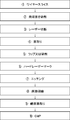
- FIG. 1 shows a flow of an example of a wafer manufacturing method of the present invention for manufacturing a wafer from a semiconductor single crystal ingot.
- a semiconductor single crystal ingot to be cut is prepared, and a wafer-like workpiece is obtained by slicing the semiconductor single crystal ingot using a wire saw (step 1 in FIG. 1).
- a plurality of wafer-like workpieces can be obtained from one semiconductor single crystal ingot.
- the wire saw a general wire saw as shown in FIG. 2 can be used.
- As the semiconductor single crystal ingot a silicon single crystal ingot, a compound semiconductor ingot, or the like can be prepared.
- a wafer-like workpiece can be obtained by slicing the semiconductor single crystal ingot so as to be thicker than before. More specifically, it is preferable to slice the semiconductor single crystal ingot so that the thickness of the wafer-like workpiece is more than twice the thickness of the product wafer. By slicing with such a thickness, it is possible to reliably secure a wafer removal allowance in subsequent grinding, etching, polishing and the like.
- the thickness of the wafer-shaped workpiece is not particularly limited because it varies depending on the thickness of the product wafer and the machining allowance in the subsequent process.
- the thickness may be 1750 ⁇ m to 1950 ⁇ m.
- the wafer-like workpiece may be sliced so as to exceed three times the thickness of the wafer as a product.
- the thickness of the wafer-shaped workpiece is the distance between wires in a wire row formed by winding a large number of wires 102 around a plurality of rollers 103 (also referred to as a wire pitch). ) Can be adjusted appropriately.
- both end faces of the wafer-like workpiece may be ground to obtain a smooth surface (step 2 in FIG. 1).
- a plurality of wafers are obtained from each wafer-like workpiece by dividing the wafer-like workpiece in the thickness direction using a laser (step 3 in FIG. 1).
- Dividing the wafer-like workpiece with a laser may be performed by the method described in Patent Document 1, for example. More specifically, as described in Patent Document 1, after forming an internal modified layer in a direction parallel to the main surface of the wafer-like workpiece by laser irradiation, along the internal modified layer The wafer can be obtained by peeling the wafer.
- a wafer-like workpiece can be directly cut by a laser beam, and the wafer-like workpiece can be divided in the thickness direction to obtain a wafer. .
- a wafer-like workpiece in dividing the wafer-like workpiece using this laser, it is preferable to divide the wafer-like workpiece into two or three in the thickness direction.
- the laser cutting can be performed only once or twice for each wafer-like workpiece, so that the time required for manufacturing per wafer can be further reduced while reducing the kerf cost.
- a wafer-like workpiece in the slicing with a wire saw, a wafer-like workpiece may be cut out with a thickness twice or three times that of a wafer cut out from a conventional semiconductor single crystal ingot.
- the kerf cost can be reduced without significantly reducing the productivity.
- the present invention is a particularly suitable method when the semiconductor single crystal ingot has a diameter of 300 mm or more.
- a method of reducing the diameter of the wire used as a conventional method for reducing the kerf allowance but this method becomes more difficult as the diameter of the semiconductor single crystal ingot increases.
- the present invention can easily reduce the kerf allowance even in a silicon wafer having a diameter of 300 mm or more.
- step 4 in FIG. 1 the chamfer shown in FIG. 1 (step 4 in FIG. 1), lapping or grinding (step 5 in FIG. 1), hard laser mark (step 6 in FIG. 1), etching (FIG. 1) is performed on the wafer thus manufactured.
- Step 7 double-side polishing (Step 8 in FIG. 1), mirror chamfering (Step 9 in FIG. 1), CMP (Step 10 in FIG. 1), and the like are performed to obtain a product wafer.
- Example 1 Example 1, Example 2, comparative example
- the wafer manufacturing method of the present invention Examples 1 and 2
- the conventional method Comparative Example
- the results of cutting silicon single crystal ingots of the same length were compared.
- a silicon single crystal ingot was cut by a flow according to the wafer manufacturing method of the present invention as shown in FIG. 1 to manufacture a plurality of silicon wafers.
- the silicon single crystal ingot was cut by the flow according to the conventional method as shown in FIG. 1 and 3 were cut so that the thickness of the silicon wafer in steps 4 and 4 ′ was 880 ⁇ m in all of Examples 1, 2 and Comparative Example.
- a comparative example will be described.
- a silicon single crystal ingot having a diameter of 300 mm and a length of 300 mm was cut into a plurality of wafers having a thickness of 880 ⁇ m.
- a wire having a diameter of 140 ⁇ m was used, and a tension of 2.5 kgf was applied, and the wire was reciprocated at a cycle of 60 s / c at an average speed of 600 m / min and cut.
- As the slurry a mixture of GC # 1500 (silicon carbide abrasive grains having an average particle diameter of 8 ⁇ m) and a coolant in a weight ratio of 50:50 was used.
- the slice wafer thus obtained had a thickness of 880 ⁇ m as described above, and the number of wafers obtained from one silicon single crystal ingot was 282.
- Examples 1 and 2 will be described.
- a single crystal silicon ingot having a diameter of 300 mm and a length of 300 mm was sliced using a wire saw of the type shown in FIG.
- the thickness of the wafer-like workpiece after slicing is 1790 ⁇ m (Example 1) when the number of divisions by cutting using a laser performed later is 2 (Example 1), and in the case of 3
- the wire pitch at the time of slicing was adjusted so as to be 2680 ⁇ m (Example 2).
- both surfaces of the wafer-like workpieces thus obtained were ground by 10 ⁇ m for a total of 20 ⁇ m to obtain a smooth surface, and then two wafers were cut by laser cutting (implemented)
- a wafer having a thickness of 880 ⁇ m was manufactured by dividing into Example 1) or 3 sheets (Example 2).
- the number of wafers obtained by this method was 300 in Example 1 when the number of divisions by laser cutting was 2, and 306 in Example 2 when the number of divisions was 3.
- the laser cutting method includes irradiating the laser from the direction of the ground surface after slicing with a wire saw, and internally modifying the wafer-like workpiece in a direction parallel to the main plane. And the wafer was peeled along the internal modified layer.
- the position where the internal modified layer is formed is 1/2 the thickness of the workpiece before laser irradiation in Example 1, and 1/3 the depth of the workpiece before laser irradiation in Example 2. That's it.
- Example 1 the work was divided into two parts by irradiating a laser on an arbitrary one side of the work and peeling one wafer.
- Example 2 first, a laser is irradiated on an arbitrary surface of a workpiece to separate one wafer, and then the other surface is irradiated with a laser under the same conditions to form one wafer.
- the workpiece was divided into three pieces by peeling.
- Table 1 summarizes the results of the comparative example and Examples 1 and 2.
- Example 1 the number of wafers obtained from ingots of the same length could be increased by 6.4% in Example 1 and 8.5% in Example 2 with respect to the comparative example. Further, in Examples 1 and 2, the amount of silicon that becomes chips by processing could be reduced by 34.7% and 45.4%, respectively, as compared with the comparative example. In Examples 1 and 2, no significant increase in the ingot cutting time was observed.
- the present invention is not limited to the above embodiment.
- the above-described embodiment is an exemplification, and the present invention has any configuration that has substantially the same configuration as the technical idea described in the claims of the present invention and that exhibits the same effects. Are included in the technical scope.
Landscapes
- Engineering & Computer Science (AREA)
- Mechanical Engineering (AREA)
- Optics & Photonics (AREA)
- Physics & Mathematics (AREA)
- Chemical Kinetics & Catalysis (AREA)
- Oil, Petroleum & Natural Gas (AREA)
- General Chemical & Material Sciences (AREA)
- Plasma & Fusion (AREA)
- Chemical & Material Sciences (AREA)
- Mechanical Treatment Of Semiconductor (AREA)
- Processing Of Stones Or Stones Resemblance Materials (AREA)
- Finish Polishing, Edge Sharpening, And Grinding By Specific Grinding Devices (AREA)
- Laser Beam Processing (AREA)
Abstract
本発明は、半導体単結晶インゴットを切断することでウェーハを製造する方法であって、ワイヤソーを用いて半導体単結晶インゴットをスライスすることでウェーハ状のワークを得た後に、レーザーを用いてウェーハ状のワークを厚さ方向に分割することで、それぞれのウェーハ状のワークから複数のウェーハを得ることを特徴とするウェーハの製造方法である。これにより、シリコンインゴットや化合物半導体インゴット等の半導体単結晶インゴットをウェーハ状に切断する方法において、生産性を大きく落とすことなく、カーフ代を削減可能なウェーハの製造方法が提供される。
Description
本発明は、ウェーハの製造方法に関する。
従来、例えば、シリコンインゴットや化合物半導体インゴット等の半導体単結晶インゴットからウェーハを切り出す手段として、ワイヤソーが知られている。このワイヤソーでは、複数のローラの周囲に切断用ワイヤが多数巻掛けられることによりワイヤ列が形成されており、その切断用ワイヤが軸方向に高速駆動され、かつ、スラリが適宜供給されながらワイヤ列に対して半導体単結晶インゴットが切り込み送りされることにより、この半導体単結晶インゴットが各ワイヤ位置で同時に切断されるようにしたものである。
ここで、図2に、一般的なワイヤソーの一例の概要を示す。図2に示すように、このワイヤソー101は、主に、半導体単結晶インゴットWを切断するためのワイヤ102(高張力鋼線)、ワイヤ102を巻掛けた溝付きローラ103、ワイヤ102に張力を付与するための機構104、104’、切断される半導体単結晶インゴットWを下方へと送り出す機構105、切断時にGC(炭化ケイ素)砥粒等を液体に分散させたスラリ109を供給する機構106で構成されている。
ワイヤ102は、一方のワイヤリール107から繰り出され、張力付与機構104を経て、溝付きローラ103に入っている。ワイヤ102はこの溝付きローラ103に300~400回程度巻掛けられた後、もう一方の張力付与機構104’を経てワイヤリール107’に巻き取られている。
また、溝付きローラ103は鉄鋼製円筒の周囲にポリウレタン樹脂を圧入し、その表面に一定のピッチで溝を切ったローラであり、巻掛けられたワイヤ102が、駆動用モータ110によって予め定められた周期で往復方向に駆動できるようになっている。
なお、半導体単結晶インゴットWの切断時には、ワーク送り機構105によって半導体単結晶インゴットWは保持されつつ押し下げられ、溝付きローラ103に巻掛けられたワイヤ102に送り出される。このようなワイヤソー101を用い、ワイヤ102にワイヤ張力付与機構104を用いて適当な張力をかけて、駆動用モータ110によりワイヤ102を往復方向に走行させながらスラリ109をノズル108を介して供給し、ワーク送り機構105で半導体単結晶インゴットを切り込み送りすることで半導体単結晶インゴットを切断する。
また、上記において砥粒を含むスラリを使用せず、代わりにダイヤモンド砥粒等をワイヤの表面に固着した固定砥粒ワイヤを使用して、ワークを切断する方法も知られている。この固定砥粒ワイヤによる切断では、図2に示したワイヤソーの鋼線ワイヤの代わりに固定砥粒ワイヤを装着し、スラリを砥粒が含まない冷却水に変えることで、ワイヤソーをそのまま使用することができる。
このようにして半導体単結晶インゴットからスライスされたウェーハは、その後、図3に示すフローのような、面取り、ラップ又は研削、ハードレーザーマーク、エッチング、両面研磨、鏡面面取り、CMP(化学機械研磨)等の工程を経て製品となる。
しかし、上記のようなワイヤソーによるワークの切断方法では、切断に伴って切り屑となるシリコンの量、いわゆるカーフ代(カーフロス)が大きいという問題がある。例えば、直径140μmのワイヤと、平均粒径が8μmのGC砥粒(GC#1500)を用いた場合、カーフ代は約170μmとなる。すなわち、ウェーハ1枚あたり170μmの厚さ分の切り屑が発生することとなる。
これに対して、カーフ代を少なくできる切断方法としてレーザーを用いた切断方法が提案されている(例えば、特許文献1)。この方法によれば、カーフ代を、ワイヤソーを用いた場合の1/10程度と小さくすることができるが、インゴットからウェーハを1枚ずつ切り出す加工方法となるため、1回の切断で数百枚のウェーハが得られるワイヤソーと比較して、ウェーハ1枚あたりにかかる加工時間が極めて長い。このため、この方法では生産性が著しく低下して、ウェーハの製造コストが、カーフ代が減少する分を超えて増大する問題がある。
本発明は前述のような問題に鑑みてなされたもので、シリコンインゴットや化合物半導体インゴット等の半導体単結晶インゴットをウェーハ状に切断する方法において、生産性を大きく落とすことなく、カーフ代を削減可能なウェーハの製造方法を提供することを目的とする。
上記目的を達成するために、本発明は、半導体単結晶インゴットを切断することでウェーハを製造する方法であって、ワイヤソーを用いて前記半導体単結晶インゴットをスライスすることでウェーハ状のワークを得た後に、レーザーを用いて前記ウェーハ状のワークを厚さ方向に分割することで、それぞれの前記ウェーハ状のワークから複数のウェーハを得ることを特徴とするウェーハの製造方法を提供する。
このように、ワイヤソーにより半導体単結晶インゴットをウェーハ状のワークにスライスする場合、通常通りウェーハを切り出す場合よりもワイヤ列のワイヤ間隔を大きくとって厚く切ることができるので、半導体単結晶インゴットを切断するワイヤの本数が少なくなり、カーフ代を削減できる。また、このようにして得たウェーハ状のワークを、カーフ代のより少ないレーザーを用いて分割することで、さらにカーフ代を低減できる。また、予めワイヤソーでインゴットを短く切ったウェーハ状のワークを、レーザーを用いて分割することで、レーザーによる切断回数を低減できるため、加工時間の大幅な増加を防ぐことができる。
このとき、前記ワイヤソーを用いた前記半導体単結晶インゴットのスライスにおいて、前記ウェーハ状のワークの厚みが、製品となるウェーハの厚みの2倍を超える厚みとなるように前記半導体単結晶インゴットをスライスすることが好ましい。
このようにすれば、レーザーを用いた分割により得られたウェーハを製品化するための、ラップ、研削、エッチング、研磨などの厚みを減ずるような処理における取り代を確保でき、最終的に所望の厚さの製品ウェーハを得ることができる。
また、前記レーザーを用いた前記ウェーハ状のワークの分割において、前記ウェーハ状のワークを厚さ方向に2枚又は3枚に分割することが好ましい。
このようにすれば、カーフ代を削減しつつ、ウェーハ1枚あたりの製造にかかる時間をより低減することができる。
また、前記半導体単結晶インゴットを直径が300mm以上のものとすることができる。
本発明のウェーハの製造方法は、半導体単結晶インゴットの直径が300mm以上である場合に特に効果的である。
本発明のウェーハの製造方法であれば、シリコンインゴットや化合物半導体インゴット等の半導体単結晶インゴットをウェーハ状に切断する方法において、生産性を大きく落とすことなく、カーフ代を削減できる。
以下、本発明について実施の形態を説明するが、本発明はこれに限定されるものではない。
図1に半導体単結晶インゴットからウェーハを製造する本発明のウェーハの製造方法の一例のフローを示す。まず、切断対象となる半導体単結晶インゴットを準備し、ワイヤソーを用いて半導体単結晶インゴットをスライスすることでウェーハ状のワークを得る(図1の工程1)。このとき、一本の半導体単結晶インゴットから複数のウェーハ状のワークを得ることができる。また、ワイヤソーとしては、図2に示すような一般的なワイヤソーを用いることができる。半導体単結晶インゴットとしては、シリコン単結晶インゴット、や化合物半導体インゴットなどを準備することができる。
このとき本発明では、半導体単結晶インゴットを従来よりも厚みが厚くなるようにスライスすることでウェーハ状のワークを得ることができる。より具体的には、ウェーハ状のワークの厚みが、製品となるウェーハの厚みの2倍を超える厚みとなるように半導体単結晶インゴットをスライスすることが好ましい。このような厚みでスライスすれば、後工程の研削、エッチング、研磨などにおけるウェーハの取り代を確実に確保できる。ウェーハ状のワークの厚みは、製品となるウェーハの厚みや後工程での加工取り代に応じて変わるため、特に限定されることは無いが、例えば、ワークが直径300mmのシリコンウェーハの場合には1600μm~1800μm、ワークが直径450mmのシリコンウェーハの場合には1750μm~1950μmとすることができる。また、ウェーハ状のワークを後工程で3枚に分割する場合は、当然、スライスにおいて製品となるウェーハの厚みの3倍を超えるようにスライスすればよい。
ウェーハ状のワークの厚みは、例えば、図2のようなワイヤソーにおいては、複数のローラ103の周囲にワイヤ102が多数巻掛けられることにより形成されるワイヤ列のワイヤ同士の間隔(ワイヤピッチとも呼ぶ)を適切に設定することで調整できる。
また、ワイヤソーによるスライス工程の次に、ウェーハ状のワークの両端面を研削して平滑な表面としてもよい(図1の工程2)。
次に、レーザーを用いてウェーハ状のワークを厚さ方向に分割することで、それぞれのウェーハ状のワークから複数のウェーハを得る(図1の工程3)。レーザーによるウェーハ状のワークの分割は、例えば、特許文献1に記載の方法により行えばよい。より具体的には、特許文献1に記載のように、レーザー照射により、ウェーハ状のワークの内部に、その主表面に平行な方向に内部改質層を形成した後に、内部改質層に沿ってウェーハを剥離することでウェーハを得ることができる。その他にも、例えば、特開2009-269296号に記載されているように、レーザービームによって直接ウェーハ状のワークを切削し、ウェーハ状のワークを厚さ方向に分割してウェーハを得ることもできる。
本発明では、このレーザーを用いたウェーハ状のワークの分割において、ウェーハ状のワークを厚さ方向に2枚又は3枚に分割することが好ましい。これにより、レーザーによる切断がウェーハ状のワーク1つあたり1~2回程度で済むので、カーフ代を削減しつつ、ウェーハ1枚あたりの製造にかかる時間をより低減することができる。この場合、ワイヤソーによるスライスにおいて、従来の半導体単結晶インゴットから切り出されるウェーハの2倍又は3倍の厚さでウェーハ状のワークを切り出しておけばよい。
以上のようにして半導体単結晶インゴットを切断してウェーハを製造することで、生産性を大きく落とすことなく、カーフ代を削減できる。
また、本発明は、半導体単結晶インゴットを直径が300mm以上のものとする場合に特に好適な方法である。ワイヤソーを用いてワークをスライスする際に、カーフ代を少なくする従来の方法として、使用するワイヤの直径を細くする方法があるが、この方法は半導体単結晶インゴットの直径が大きくなるほど難易度が高くなる。一方、本発明は直径が300mm以上のシリコンウェーハにおいても容易にカーフ代を削減できる。
また、このようにして製造したウェーハに、図1に示す面取り(図1の工程4)、ラップ又は研削(図1の工程5)、ハードレーザーマーク(図1の工程6)、エッチング(図1の工程7)、両面研磨(図1の工程8)、鏡面面取り(図1の工程9)、CMP(図1の工程10)などの処理を施して製品ウェーハとする。
以下、本発明の実施例及び比較例を示して本発明をより具体的に説明するが、本発明はこれら実施例に限定されるものではない。
(実施例1、実施例2、比較例)
本発明のウェーハの製造方法(実施例1、2)と従来の方法(比較例)とで、それぞれ同じ長さのシリコン単結晶インゴットを切断した際の結果を比較した。実施例1、2では、図1のような本発明のウェーハ製造方法に従ったフローでシリコン単結晶インゴットを切断して複数のシリコンウェーハを製造した。一方、比較例では、図3のような従来の方法に従ったフローでシリコン単結晶インゴットを切断した。また、図1、3の工程4及び4’におけるシリコンウェーハの厚さを、実施例1、2、比較例の全てで880μmとなるように切断した。また、図1、3の工程5及び5’以降の加工条件は同条件とした。
本発明のウェーハの製造方法(実施例1、2)と従来の方法(比較例)とで、それぞれ同じ長さのシリコン単結晶インゴットを切断した際の結果を比較した。実施例1、2では、図1のような本発明のウェーハ製造方法に従ったフローでシリコン単結晶インゴットを切断して複数のシリコンウェーハを製造した。一方、比較例では、図3のような従来の方法に従ったフローでシリコン単結晶インゴットを切断した。また、図1、3の工程4及び4’におけるシリコンウェーハの厚さを、実施例1、2、比較例の全てで880μmとなるように切断した。また、図1、3の工程5及び5’以降の加工条件は同条件とした。
まず、比較例について説明する。比較例では、図2に示すようなワイヤソーを用い、直径300mm、長さ300mmのシリコン単結晶インゴットを厚さ880μmの複数のウェーハ状に切断した。ワイヤは直径140μmのものを使用し、2.5kgfの張力をかけて、600m/minの平均速度で60s/cのサイクルでワイヤを往復走行させて切断した。また、スラリとしては、GC#1500(平均粒径8μmの炭化ケイ素砥粒)とクーラントを重量比50:50の割合で混ぜたものを用いた。このようにして得られたスライスウェーハの厚さは上記の通り880μmであり、一本のシリコン単結晶インゴットから得られたウェーハの枚数は282枚であった。
次に、実施例1、2について説明する。ワイヤソーを用いた切断(図1の工程1)では、図2に示すタイプのワイヤソーを用い、直径300mm、長さ300mmの単結晶シリコンインゴットをスライスしてウェーハ状のワークを得た。ただし、実施例1、2では、スライス後のウェーハ状のワークの厚さが、後で行うレーザーを用いた切断による分割数が2枚の場合は1790μm(実施例1)、3枚の場合は2680μm(実施例2)となるように、スライス時のワイヤピッチを調整した。次に、実施例1、2では、このようにして得られたウェーハ状のワークの両面を10μmずつ合計20μm研削して平滑な表面とし、続いてレーザーを用いた切断によりウェーハを2枚(実施例1)又は3枚(実施例2)に分割して、厚さ880μmのウェーハを製造した。この方法で得られたウェーハの枚数は、レーザーを用いた切断による分割数が2枚の場合の実施例1で300枚、分割数が3枚の場合の実施例2で306枚であった。
上記の実施例において、レーザーによる切断方法としては、ワイヤソーでスライスした後に研削加工した面の方向からレーザーを照射し、ウェーハ状のワークの内部に、その主平面に平行な方向に内部改質層を形成し、内部改質層に沿ってウェーハを剥離する方法で行った。内部改質層を形成する位置は、実施例1では、レーザー照射前のワーク厚さの1/2の深さであり、実施例2では、レーザー照射前のワーク厚さの1/3の深さである。実施例1では、ワークの任意の片側の面にレーザーを照射して、ウェーハを1枚剥離することにより、ワークを2枚に分割した。実施例2では、まず、ワークの任意の片側の面にレーザーを照射して、ウェーハを1枚剥離し、続いて、反対側の面にも同じ条件でレーザーを照射して、ウェーハを1枚剥離することにより、ワークを3枚に分割した。
表1に、比較例、実施例1、2の結果をまとめたものを示す。
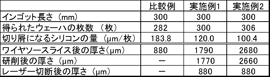
表1からわかるように、同じ長さのインゴットから得られるウェーハの枚数を、比較例に対して、実施例1で6.4%、実施例2で8.5%増やすことができた。また、実施例1、2では、加工によって切り屑となるシリコン量は、比較例に対して、それぞれ、34.7%、45.4%削減することができた。また、実施例1、2では、インゴットの切断時間の大幅な増加は見られなかった。
なお、本発明は、上記実施形態に限定されるものではない。上記実施形態は例示であり、本発明の特許請求の範囲に記載された技術的思想と実質的に同一な構成を有し、同様な作用効果を奏するものは、いかなるものであっても本発明の技術的範囲に包含される。
Claims (4)
- 半導体単結晶インゴットを切断することでウェーハを製造する方法であって、
ワイヤソーを用いて前記半導体単結晶インゴットをスライスすることでウェーハ状のワークを得た後に、レーザーを用いて前記ウェーハ状のワークを厚さ方向に分割することで、それぞれの前記ウェーハ状のワークから複数のウェーハを得ることを特徴とするウェーハの製造方法。 - 前記ワイヤソーを用いた前記半導体単結晶インゴットのスライスにおいて、前記ウェーハ状のワークの厚みが、製品となるウェーハの厚みの2倍を超える厚みとなるように前記半導体単結晶インゴットをスライスすることを特徴とする請求項1に記載のウェーハの製造方法。
- 前記レーザーを用いた前記ウェーハ状のワークの分割において、前記ウェーハ状のワークを厚さ方向に2枚又は3枚に分割することを特徴とする請求項1又は請求項2に記載のウェーハの製造方法。
- 前記半導体単結晶インゴットを直径が300mm以上のものとすることを特徴とする請求項1から請求項3のいずれか1項に記載のウェーハの製造方法。
Applications Claiming Priority (2)
| Application Number | Priority Date | Filing Date | Title |
|---|---|---|---|
| JP2017-042010 | 2017-03-06 | ||
| JP2017042010A JP6705399B2 (ja) | 2017-03-06 | 2017-03-06 | ウェーハの製造方法 |
Publications (1)
| Publication Number | Publication Date |
|---|---|
| WO2018163752A1 true WO2018163752A1 (ja) | 2018-09-13 |
Family
ID=63448920
Family Applications (1)
| Application Number | Title | Priority Date | Filing Date |
|---|---|---|---|
| PCT/JP2018/005366 Ceased WO2018163752A1 (ja) | 2017-03-06 | 2018-02-16 | ウェーハの製造方法 |
Country Status (3)
| Country | Link |
|---|---|
| JP (1) | JP6705399B2 (ja) |
| TW (1) | TW201834050A (ja) |
| WO (1) | WO2018163752A1 (ja) |
Families Citing this family (1)
| Publication number | Priority date | Publication date | Assignee | Title |
|---|---|---|---|---|
| EP3831926A4 (en) | 2018-08-06 | 2021-10-20 | Nissan Chemical Corporation | CELL CULTURE SYSTEM AND CELL MASS PRODUCTION PROCESS USING IT |
Citations (4)
| Publication number | Priority date | Publication date | Assignee | Title |
|---|---|---|---|---|
| JP2006245498A (ja) * | 2005-03-07 | 2006-09-14 | Sharp Corp | 基板の製造方法およびその装置 |
| JP2015074004A (ja) * | 2013-10-07 | 2015-04-20 | 信越ポリマー株式会社 | 内部加工層形成単結晶部材およびその製造方法 |
| JP2015123465A (ja) * | 2013-12-26 | 2015-07-06 | 信越ポリマー株式会社 | 基板加工装置及び基板加工方法 |
| JP2017092314A (ja) * | 2015-11-12 | 2017-05-25 | 株式会社ディスコ | SiC基板の分離方法 |
Family Cites Families (2)
| Publication number | Priority date | Publication date | Assignee | Title |
|---|---|---|---|---|
| JPH11170169A (ja) * | 1997-12-12 | 1999-06-29 | Toshiba Ceramics Co Ltd | 半導体ウェーハの製造方法およびその装置 |
| JPH11333708A (ja) * | 1998-06-01 | 1999-12-07 | Shin Etsu Handotai Co Ltd | ラッピング装置及び方法 |
-
2017
- 2017-03-06 JP JP2017042010A patent/JP6705399B2/ja active Active
-
2018
- 2018-02-16 WO PCT/JP2018/005366 patent/WO2018163752A1/ja not_active Ceased
- 2018-02-22 TW TW107105867A patent/TW201834050A/zh unknown
Patent Citations (4)
| Publication number | Priority date | Publication date | Assignee | Title |
|---|---|---|---|---|
| JP2006245498A (ja) * | 2005-03-07 | 2006-09-14 | Sharp Corp | 基板の製造方法およびその装置 |
| JP2015074004A (ja) * | 2013-10-07 | 2015-04-20 | 信越ポリマー株式会社 | 内部加工層形成単結晶部材およびその製造方法 |
| JP2015123465A (ja) * | 2013-12-26 | 2015-07-06 | 信越ポリマー株式会社 | 基板加工装置及び基板加工方法 |
| JP2017092314A (ja) * | 2015-11-12 | 2017-05-25 | 株式会社ディスコ | SiC基板の分離方法 |
Also Published As
| Publication number | Publication date |
|---|---|
| TW201834050A (zh) | 2018-09-16 |
| JP2018148042A (ja) | 2018-09-20 |
| JP6705399B2 (ja) | 2020-06-03 |
Similar Documents
| Publication | Publication Date | Title |
|---|---|---|
| US9707635B2 (en) | Method for slicing workpiece and wire saw | |
| WO2018173693A1 (ja) | インゴットの切断方法 | |
| US20140318522A1 (en) | Method for slicing workpiece | |
| JP6015598B2 (ja) | インゴットの切断方法及びワイヤソー | |
| JP5649692B2 (ja) | 円筒形の被加工物から多数のウェハを同時にスライスするための方法 | |
| TW201530641A (zh) | 半導體晶圓的製造方法 | |
| KR102100839B1 (ko) | 워크의 절단방법 | |
| TWI753128B (zh) | 工件的切斷方法 | |
| TWI853209B (zh) | 自半導體材料的圓柱形錠生產晶圓的方法 | |
| JP2003159642A (ja) | ワーク切断方法およびマルチワイヤソーシステム | |
| CN113226640A (zh) | 工件的切断方法及线锯 | |
| JP6705399B2 (ja) | ウェーハの製造方法 | |
| JP2002075923A (ja) | シリコン単結晶インゴットの加工方法 | |
| JP7020454B2 (ja) | ワークの切断方法及びワイヤソー | |
| CN110545957B (zh) | 工件的切断方法及接合部件 | |
| JP7429080B1 (ja) | 半導体結晶ウェハの製造装置および製造方法 | |
| JP7708004B2 (ja) | ワークの切断方法、スライス装置及びスライスベース | |
| JP5945967B2 (ja) | ワークの切断方法及びワイヤソー | |
| JP7075295B2 (ja) | ソーワイヤ、ソーワイヤの製造方法、および基板の製造方法 | |
| JP4325655B2 (ja) | 化合物半導体基板の製造方法 | |
| JP2013082020A (ja) | ワーク切断方法、半導体基板の製造方法、半導体基板およびワイヤソー装置 | |
| EP4670910A1 (en) | A PROCESS FOR GRINDING SEMICONDUCTIVE CRYSTAL AND A PROCESS FOR PRODUCING EXTENDED SIC INGOTS USING SAID GRINDING PROCESS |
Legal Events
| Date | Code | Title | Description |
|---|---|---|---|
| 121 | Ep: the epo has been informed by wipo that ep was designated in this application |
Ref document number: 18764267 Country of ref document: EP Kind code of ref document: A1 |
|
| NENP | Non-entry into the national phase |
Ref country code: DE |
|
| 122 | Ep: pct application non-entry in european phase |
Ref document number: 18764267 Country of ref document: EP Kind code of ref document: A1 |