WO2018159244A1 - 蛍光体 - Google Patents
蛍光体 Download PDFInfo
- Publication number
- WO2018159244A1 WO2018159244A1 PCT/JP2018/004247 JP2018004247W WO2018159244A1 WO 2018159244 A1 WO2018159244 A1 WO 2018159244A1 JP 2018004247 W JP2018004247 W JP 2018004247W WO 2018159244 A1 WO2018159244 A1 WO 2018159244A1
- Authority
- WO
- WIPO (PCT)
- Prior art keywords
- phosphor
- site
- phosphor according
- excitation
- light
- Prior art date
- Legal status (The legal status is an assumption and is not a legal conclusion. Google has not performed a legal analysis and makes no representation as to the accuracy of the status listed.)
- Ceased
Links
Images















Classifications
-
- C—CHEMISTRY; METALLURGY
- C09—DYES; PAINTS; POLISHES; NATURAL RESINS; ADHESIVES; COMPOSITIONS NOT OTHERWISE PROVIDED FOR; APPLICATIONS OF MATERIALS NOT OTHERWISE PROVIDED FOR
- C09K—MATERIALS FOR MISCELLANEOUS APPLICATIONS, NOT PROVIDED FOR ELSEWHERE
- C09K11/00—Luminescent materials, e.g. electroluminescent or chemiluminescent
- C09K11/08—Luminescent materials, e.g. electroluminescent or chemiluminescent containing inorganic luminescent materials
- C09K11/77—Luminescent materials, e.g. electroluminescent or chemiluminescent containing inorganic luminescent materials containing rare earth metals
- C09K11/7728—Luminescent materials, e.g. electroluminescent or chemiluminescent containing inorganic luminescent materials containing rare earth metals containing europium
- C09K11/7732—Halogenides
- C09K11/7733—Halogenides with alkali or alkaline earth metals
-
- C—CHEMISTRY; METALLURGY
- C01—INORGANIC CHEMISTRY
- C01B—NON-METALLIC ELEMENTS; COMPOUNDS THEREOF; METALLOIDS OR COMPOUNDS THEREOF NOT COVERED BY SUBCLASS C01C
- C01B25/00—Phosphorus; Compounds thereof
- C01B25/16—Oxyacids of phosphorus; Salts thereof
- C01B25/26—Phosphates
- C01B25/455—Phosphates containing halogen
-
- C—CHEMISTRY; METALLURGY
- C09—DYES; PAINTS; POLISHES; NATURAL RESINS; ADHESIVES; COMPOSITIONS NOT OTHERWISE PROVIDED FOR; APPLICATIONS OF MATERIALS NOT OTHERWISE PROVIDED FOR
- C09K—MATERIALS FOR MISCELLANEOUS APPLICATIONS, NOT PROVIDED FOR ELSEWHERE
- C09K11/00—Luminescent materials, e.g. electroluminescent or chemiluminescent
- C09K11/08—Luminescent materials, e.g. electroluminescent or chemiluminescent containing inorganic luminescent materials
- C09K11/70—Luminescent materials, e.g. electroluminescent or chemiluminescent containing inorganic luminescent materials containing phosphorus
- C09K11/72—Luminescent materials, e.g. electroluminescent or chemiluminescent containing inorganic luminescent materials containing phosphorus also containing halogen, e.g. halophosphates
- C09K11/73—Luminescent materials, e.g. electroluminescent or chemiluminescent containing inorganic luminescent materials containing phosphorus also containing halogen, e.g. halophosphates also containing alkaline earth metals
-
- C—CHEMISTRY; METALLURGY
- C09—DYES; PAINTS; POLISHES; NATURAL RESINS; ADHESIVES; COMPOSITIONS NOT OTHERWISE PROVIDED FOR; APPLICATIONS OF MATERIALS NOT OTHERWISE PROVIDED FOR
- C09K—MATERIALS FOR MISCELLANEOUS APPLICATIONS, NOT PROVIDED FOR ELSEWHERE
- C09K11/00—Luminescent materials, e.g. electroluminescent or chemiluminescent
- C09K11/08—Luminescent materials, e.g. electroluminescent or chemiluminescent containing inorganic luminescent materials
- C09K11/77—Luminescent materials, e.g. electroluminescent or chemiluminescent containing inorganic luminescent materials containing rare earth metals
- C09K11/7728—Luminescent materials, e.g. electroluminescent or chemiluminescent containing inorganic luminescent materials containing rare earth metals containing europium
- C09K11/7729—Chalcogenides
- C09K11/7731—Chalcogenides with alkaline earth metals
-
- C—CHEMISTRY; METALLURGY
- C09—DYES; PAINTS; POLISHES; NATURAL RESINS; ADHESIVES; COMPOSITIONS NOT OTHERWISE PROVIDED FOR; APPLICATIONS OF MATERIALS NOT OTHERWISE PROVIDED FOR
- C09K—MATERIALS FOR MISCELLANEOUS APPLICATIONS, NOT PROVIDED FOR ELSEWHERE
- C09K11/00—Luminescent materials, e.g. electroluminescent or chemiluminescent
- C09K11/08—Luminescent materials, e.g. electroluminescent or chemiluminescent containing inorganic luminescent materials
- C09K11/77—Luminescent materials, e.g. electroluminescent or chemiluminescent containing inorganic luminescent materials containing rare earth metals
- C09K11/7783—Luminescent materials, e.g. electroluminescent or chemiluminescent containing inorganic luminescent materials containing rare earth metals containing two or more rare earth metals one of which being europium
- C09K11/7784—Chalcogenides
- C09K11/7786—Chalcogenides with alkaline earth metals
-
- C—CHEMISTRY; METALLURGY
- C09—DYES; PAINTS; POLISHES; NATURAL RESINS; ADHESIVES; COMPOSITIONS NOT OTHERWISE PROVIDED FOR; APPLICATIONS OF MATERIALS NOT OTHERWISE PROVIDED FOR
- C09K—MATERIALS FOR MISCELLANEOUS APPLICATIONS, NOT PROVIDED FOR ELSEWHERE
- C09K11/00—Luminescent materials, e.g. electroluminescent or chemiluminescent
- C09K11/08—Luminescent materials, e.g. electroluminescent or chemiluminescent containing inorganic luminescent materials
- C09K11/77—Luminescent materials, e.g. electroluminescent or chemiluminescent containing inorganic luminescent materials containing rare earth metals
- C09K11/7783—Luminescent materials, e.g. electroluminescent or chemiluminescent containing inorganic luminescent materials containing rare earth metals containing two or more rare earth metals one of which being europium
- C09K11/779—Halogenides
- C09K11/7791—Halogenides with alkali or alkaline earth metals
Definitions
- the present invention relates to a phosphor.
- white light emitting diodes have become widespread as alternative light sources for fluorescent lamps and incandescent bulbs. Such white LEDs are also required to have high color rendering properties close to natural light as in the case of conventional light sources.
- the current mainstream white LED is generally a combination of a blue light emitting semiconductor light emitting element and a yellow phosphor.
- the pseudo white color obtained by synthesizing blue light and yellow light has a short red component, and it has been difficult to achieve high color rendering. Therefore, in order to realize high color rendering properties, a white LED using a mixed phosphor in which a red phosphor supplementing a red component is combined with a yellow phosphor (or a green phosphor) has been devised.
- red phosphors having compositions such as CaAlSiN 3 : Eu, (Ca, Sr) AlSiN 3 : Eu, and Ca 2 Si 5 N 8 : Eu have been developed. (See Patent Documents 1 to 3).
- the conventional red phosphors are mainly nitrides including the phosphors having the above composition.
- the synthesis of the nitride phosphor requires a special environment such as a deoxygenated atmosphere and high temperature and pressure, which increases the manufacturing cost.
- the red phosphor described above has an excitation end between 500 and 550 nm. Therefore, when such a red phosphor is used together with a phosphor that emits light of another color in order to realize white light, it absorbs the light emitted by the phosphor of blue, green, yellow, etc. and converts it into red. Resulting in. As a result, it is difficult to adjust the color because the chromaticity may deviate greatly from the desired emission color with respect to slight variations in the phosphor content and the coating form. It also causes a decrease in luminous efficiency.
- the present invention has been made in view of such circumstances, and an object of the present invention is to provide a novel phosphor.
- a phosphor according to an embodiment of the present invention has a perovskite crystal structure in which a light-emitting site is represented by ABX 3 (A and B are cations and X is an anion), and the perovskite crystal structure The luminescent element is located at the B site which is the heart.
- a novel phosphor having a perovskite crystal structure at the light emitting site can be realized.
- X may be composed of two or more anions.
- the electron density related to the bond of the BX 6 octahedron composed of the cation B and the anion X can be made non-uniform.
- the crystal field splitting becomes large, and a phosphor that emits light when excited by relatively low energy light can be realized.
- the anion may be composed of two or more elements selected from the group consisting of oxygen, halogen and nitrogen.
- the anion may be composed of oxygen and fluorine.
- B may be one or more cations selected from the group consisting of Eu 2+ , Ce 3+ , Sm 2+ and Yb 2+ . This facilitates the 4f-5d transition.
- Ionic radius I A cationic positioned at the A site of the perovskite crystal structure is greater than the ionic radius I B cations located at the B site.
- Oxygen as an anion located at the X site of the perovskite crystal structure and MO 4 (M is a trivalent to pentavalent metal element) tetrahedral structure oxygen may be shared.
- a novel phosphor can be provided.
- FIG. 6A is a diagram schematically illustrating a hexacoordinate BX 6 octahedron
- FIG. 6B is a diagram for explaining an energy state of a 5d orbit in hexacoordinate. It is the figure which showed typically the expansion of the divided orbit.
- FIG. 3 is a diagram showing an X-ray diffraction pattern of a phosphor according to Example 1.
- FIG. It is a figure which shows the result of the resonance spectrum measured without decoupling. It is a figure which shows the result of the resonance spectrum which erase
- 31 is a diagram showing the results of P ⁇ 19 F ⁇ CP-CPMAS measuring. It is a schematic diagram which shows the crystal structure of the fluorescent substance which concerns on this Embodiment. It is a figure for demonstrating the crystal structure which a luminescent site has. It is the schematic diagram which looked at the crystal structure of the fluorescent substance shown in FIG. 12 from another direction.
- FIG. It is a figure which shows the emission spectrum at the time of irradiating the ultraviolet-ray of high energy to the fluorescent substance which concerns on Example 1.
- FIG. It is a figure which shows the diffuse reflection spectrum of the fluorescent substance which concerns on Example 1.
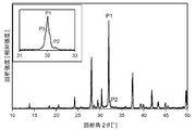
- FIG. It is a figure which shows the X-ray-diffraction pattern of the fluorescent substance which concerns on Example 2.
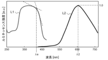
- FIG. It is a figure which shows the excitation spectrum and emission spectrum of the fluorescent substance which concern on Example 2.
- FIG. It is a figure which shows the X-ray-diffraction pattern of the fluorescent substance which concerns on Example 3.
- FIG. It is a figure which shows the excitation spectrum and emission spectrum of the fluorescent substance which concern on Example 3.
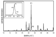
- FIG. It is a figure which shows the X-ray-diffraction pattern of the fluorescent substance which concerns on Example 4.
- FIG. It is a figure which shows the excitation spectrum and emission spectrum of the fluorescent substance which concern on Example 4. It is a figure which shows the X-ray-diffraction pattern of the fluorescent substance which concerns on Example 5. FIG. It is a figure which shows the excitation spectrum and emission spectrum of the fluorescent substance which concern on Example 5. FIG. It is a figure which shows the X-ray-diffraction pattern of the fluorescent substance which concerns on Example 6. FIG. It is a figure which shows the excitation spectrum and emission spectrum of the fluorescent substance which concern on Example 6. FIG. It is a figure which shows the X-ray-diffraction pattern of the fluorescent substance which concerns on Example 7. FIG. It is a figure which shows the excitation spectrum and emission spectrum of the fluorescent substance which concern on Example 7. FIG.
- FIG. 8 It is a figure which shows the X-ray-diffraction pattern of the fluorescent substance which concerns on Example 8.
- FIG. It is a figure which shows the excitation spectrum and emission spectrum of the fluorescent substance which concern on Example 8.
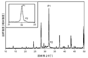
- FIG. It is a figure which shows the X-ray-diffraction pattern of the fluorescent substance which concerns on Example 9.
- FIG. It is a figure which shows the excitation spectrum and emission spectrum of the fluorescent substance which concern on Example 9.
- the phosphor according to the present embodiment is a phosphor that is efficiently excited and emits light by ultraviolet rays or short-wavelength visible light. Specifically, it is a phosphor that exhibits strong excitation with near-ultraviolet light or short-wavelength visible light of 420 nm or less and emits red light with an emission spectrum peak wavelength of 600 nm or more. In addition, the phosphor according to the present embodiment achieves red light emission by doping a host crystal of a halo oxide with an activator such as Eu 2+ ions.
- the phosphor according to the present embodiment is a red phosphor having a large Stokes shift (approximately 0.8 to 1.2 eV). Therefore, visible light emitted from other phosphors such as blue, green, and yellow is difficult to be absorbed.
- the Stokes shift is an energy difference between the excitation edge wavelength and the peak wavelength of the emission spectrum.
- the excitation end wavelength indicates a wavelength at which a decrease in excitation intensity on the long wavelength side in the excitation spectrum starts to rapidly decrease.
- a phosphor corresponding to the light of a semiconductor light emitting device having a high excitation light density needs a fast excitation-emission cycle.
- a 4f-5d permissible transition capable of transition while maintaining the electron spin state is preferable.
- Examples of the element capable of the 4f-5d transition include rare earth elements such as Eu 2+ , Ce 3+ , Sm 2+ , and Yb 2+ .
- the outer shell orbit of these rare earth elements is 6s, and the inner shell has a 4f orbit.
- electrons in the 4f orbit transition to the 5d orbit located in the outer shell, thereby forming an excited state.
- the greater the spread of the electron cloud in the 5d orbit the lower the energy level of this orbit and the higher the transition probability.
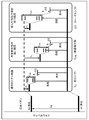
- FIG. 1 is a diagram for explaining the mechanism of excitation and emission according to the crystal state. Excitation at low energy requires a complex (or distorted low-symmetry structure) emission site structure or covalent bonding.
- energy of 4.0 eV or more is required for 4f-5d transition in free ions.
- no transition occurs in the light of the semiconductor light emitting element that emits near ultraviolet light or short wavelength visible light having a wavelength of about 380 to 450 nm. Therefore, in order to lower the 4f-5d transition energy, it is effective to dope the crystal and coordinate anions around the rare earth ions.
- the 5d orbital is reduced in energy by two actions (center of gravity shift E c and crystal field splitting E cfs ) due to the coordination of anions.
- Centroid shift E c by anion is coordinated to the rare earth element (cation), due to the influence of the negative charge around the entire five 5d orbitals are low energy reduction.
- the effect is small when the coordinating anion is ionic bond, and increases when the covalent bond is increased.
- the crystal field splitting E cfs is that the degeneration of five 5d orbitals is solved by the three-dimensional structure in which an anion is coordinated with a rare earth element (cation), and the energy level (orbital level) of the 5d orbitals is split.
- the 5d orbit in the direction where there is no anion has little electrostatic repulsion with the anion, and the electron cloud of the 5d orbit tends to spread (the energy level becomes low).
- the direction in which the anions are coordinated increases the electrostatic repulsion and increases the energy level. In other words, a distorted ligand field is required to greatly disrupt the degeneration of the 5d orbital.
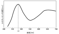
- FIG. 2 is a diagram showing an example of an excitation spectrum and an emission spectrum of a general red phosphor based on nitride.
- Red phosphors that have become popular in recent years are phosphors based on nitrides such as CaAlSiN 3 : Eu and Ca 2 Si 5 N 8 : Eu. Since these phosphors increase the center-of-gravity shift by increasing the covalent bond, the excitation band (excitation spectrum) extends to the long wavelength side as shown in FIG. Instead, it absorbs blue, green and yellow visible light.
- FIG. 3 is a schematic diagram for explaining the Stokes shift.
- Stokes shift is caused by relaxation of the crystal structure in the excited state.
- the excited electron orbit approaches the coordination anion.
- the position of the lighter (smaller atomic weight) anion than the cation (rare earth) shifts.
- the crystal structure of the excited state differs from the ground state. After the crystal structure change (relaxation 1) in the excited state occurs, the crystal returns to the ground state, and light emission occurs accordingly.
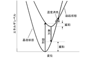
- FIG. 4 is a schematic diagram showing coordination coordinates.
- the vertical axis of coordination coordinates indicates the energy level of the valence electron of the light emitting element, and the horizontal axis indicates the displacement with the distance between the light emitting element and the anion having the lowest energy level in the ground state of the crystal being zero.
- the 4f electrons of the luminescent element increase in energy level and enter an excited state at the moment when the excitation light is absorbed.
- the excited state relaxation that eliminates electrostatic repulsion with the coordination anion occurs, and the energy level decreases to an equilibrium state. Since light emission starts from that point, an energy transition smaller than the excitation energy and a long wavelength shift occur. At this time, it is the phonon oscillation that must be taken into consideration.
- the phonon vibration increases. In that case, the energy level of the system increases.
- the temperature rises and becomes equal to the vibration level of the ground state due to phonon vibration in the excited state a non-radiative transition occurs. In general, when the Stokes shift becomes large, there is a concern that the temperature characteristic is deteriorated.
- the present inventors have conceived the possibility of a phosphor having a new crystal structure that increases the Stokes shift.
- Excitation / emission of the phosphor is caused by electron orbital transition in the emission center element. Therefore, a light emitting element (for example, Eu 2+ , Ce 3+ ) having a 4f-5d transition with a high transition speed is desirable for a phosphor in a high-intensity light source such as a white LED.
- a light emitting element for example, Eu 2+ , Ce 3+
- electrons in the 4f orbit in the inner shell of the 6s orbit absorb the excitation energy, and transition to the 5d orbit spreading in the outer shell of the 6s orbit.
- Light emission occurs by returning from the 5d orbit to the 4f orbit. Therefore, in order to show a large Stokes shift, it is important that the spread of the 5d orbit in the excited state becomes large.
- the spread of the 5d orbit is determined by the crystal structure around the light emitting element. Therefore, the inventors of the present application devised a crystal structure that increases the 5d orbital spread.
- FIG. 5 is a diagram showing a perovskite crystal structure.
- the perovskite crystal represented by the composition formula ABX 3 ideally has a cubic unit cell, with metal A at each vertex (A site) of the cubic crystal and metal B at the body center site (B site). However, an anion X is arranged at each face center site (X site) of the cubic crystal. In addition, six anions X coordinate with metal B to form a BX 6 octahedron.
- a light emitting element that makes a 4f-5d transition is located at the B site.
- the phosphor according to the present embodiment is a novel phosphor having a perovskite crystal structure at the light emitting site.
- the anion X forming the BX 6 octahedron may be composed of two or more types of anions. Specifically, one of the anions X is oxygen. Another kind of anion X is halogen. Of the halogens, fluorine is particularly preferred. As another form, another anion X other than oxygen may be nitrogen.
- the A site according to the present embodiment is occupied by monovalent or divalent cations having a large ionic radius.
- Ionic radius I A cationic positioned at the A site is greater than the ionic radius I B of the light emitting element positioned at a B-site.
- the ion radius I A may be greater than 10% than the ionic radius I B.
- the cation occupying the A site may be composed of a monovalent cation, may be composed of a divalent cation, or may be composed of both.
- the phosphor according to the present embodiment configured as described above can be excited with low energy and has a large Stokes shift.
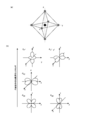
- FIG. 6A is a diagram schematically illustrating a hexacoordinate BX 6 octahedron
- FIG. 6B is a diagram for explaining an energy state of a 5d orbit in hexacoordinate.
- a mixed ligand plural kinds of ligands
- a general perovskite structure is represented by ABO 3 , and six oxygen ions are coordinated to the B site. Therefore, the B site has strong ion binding properties, high symmetry, and little distortion of the ligand field. For this reason, excitation is difficult with a small energy such as light having a wavelength (380 to 450 nm) of a semiconductor light emitting element used in a white LED.
- two or more kinds of anions X are coordinated to the B site of the light emitting site, thereby making the electron density related to the bond of the BX 6 octahedron nonuniform.
- the crystal field splitting increases, and the excitation band decreases to the energy level excited by the light emission (low energy) of the semiconductor light emitting device used in the white LED.
- the energy level of t 2 g orbit than e g orbitals decreases. Even in the t 2g orbit, the energy level in the d xz and d yz directions where the density of the anion X is low decreases.
- FIG. 7 is a diagram schematically showing the spread of the split orbit.
- the split d xz and d yz orbits extend in the direction of the A site located at each vertex of the cubic crystal.
- the cation at the A site is positively charged.
- the electrons in the d xz and d yz orbits spreading from the B site are attracted to the A site (the cations on the A site are not attracted by electrostatic attraction because of their large ionic radius and mass).
- the phosphor according to the present embodiment exhibits stable temperature characteristics despite a large Stokes shift.
- the first phosphor for example, red phosphor
- the second phosphor that emits fluorescence having a color different from that of the first phosphor (for example, blue phosphor, green phosphor, yellow fluorescence).
- a semiconductor light-emitting element that emits light that excites the first phosphor and the second phosphor have the following effects.
- the first phosphor according to the present embodiment since there is almost no absorption of the first phosphor according to the present embodiment in a wavelength range longer than the emission wavelength of the semiconductor light emitting element, when mixed with the second phosphor of other emission color, Misalignment is less likely to occur. Second, since the first phosphor according to the present embodiment does not cause relaxation of the excited state due to the movement of the anion, the temperature characteristic is small despite the fact that the crystal structure change due to excitation is small and the Stokes shift is large. It becomes good.
- Example 1 In the phosphor according to Example 1, the elements constituting the crystal structure ABX 3 of the light emitting site are: The cation A is K + , the cation B is Eu 2+ , and the anion X is O 2 ⁇ and F ⁇ . In addition to Eu 2+ , Ce 3+ , Sm 2+ , Yb 2+, etc. may be added as the cation B. This facilitates the 4f-5d transition. Further, the cation M constituting the tetrahedron MO 4 that connects the perovskite structures of the light emitting sites is P 5+ . M may be a trivalent to pentavalent metal element.
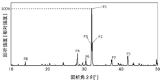
- FIG. 8 is a diagram showing an X-ray diffraction pattern of the phosphor according to Example 1.
- the diffraction angle 2 ⁇ is 31.0 ° to 33.33.
- the first diffraction peak P1, the second diffraction peak P2, and the third diffraction peak P3 exist in the range of 0 °, and the diffraction intensity of the first diffraction peak P1 having the highest intensity is 100, the second diffraction peak P2
- the diffraction intensity of the third diffraction peak P3 is 30-50.
- a fourth diffraction peak P4 having a diffraction intensity of 15 to 25 is present in a diffraction angle 2 ⁇ range of 27.0 ° to 29.0 °. Further, the diffraction angle 2 ⁇ has a fifth diffraction peak P5 having a diffraction intensity of 15 to 25 in the range of 41.0 ° to 43.0 °. Further, the diffraction angle 2 ⁇ has a sixth diffraction peak P6 having a diffraction intensity of 10 to 15 in the range of 29.0 ° to 31.0 °.
- the diffraction angle 2 ⁇ has a seventh diffraction peak P7 having a diffraction intensity of 10 to 15 in the range of 36.0 ° to 39.0 °. Further, the diffraction angle 2 ⁇ has an eighth diffraction peak P8 having a diffraction intensity of 5 to 10 in the range of 13.0 ° to 15.0 °.
- the above-mentioned crystal is a crystal having a new structure that is not registered in ICDD (International Center for Diffraction Date), which is an X-ray diffraction database widely used for X-ray diffraction.
- ICDD International Center for Diffraction Date
- the phosphor of Example 1 contains oxygen and fluorine in the anion.
- Oxygen and fluorine are elements that are adjacent to each other in the periodic table, and it is difficult to specify their occupied positions only from X-ray diffraction data.
- solid NMR measurement of the sample according to Example 1 was performed.
- solid-state NMR the bonding state of an element having a spin quantum number of 1/2 can be grasped, and the bonding relationship between 19 F and 31 P can be examined.
- the measurement was performed using JNM-ECZ500R (manufactured by JEOL Ltd.) having a magnetic field intensity of 11.7 T (500 MHz).
- a sample of about 50 ⁇ L was packed in a 3.2 mm measurement probe and measured at room temperature (about 23 ° C.).
- FIG. 9 is a diagram showing the result of the resonance spectrum measured without decoupling. As shown in FIG. 9, resonance spectra were confirmed at 0.64 ppm and 0.76 ppm. Next, a radio wave (470.6 MHz) corresponding to a 19 F magnetorotation ratio was irradiated to eliminate the PF interaction, and decoupling measurement was performed.
- FIG. 10 is a diagram showing the result of a resonance spectrum obtained by decoupling measurement after eliminating the PF interaction. As shown in FIG. 10, the resonance spectrum changed to a single broad signal. This result indicates that F has some interference with the atomic vibration of P, but it has not been possible to determine the presence or absence of coupling.
- FIG. 11 is a diagram showing the results of 31 P ⁇ 19 F ⁇ CP-CPMAS measurement. As shown in FIG. 11, even when the contact time was extended to 20000 ⁇ s, the maximum value of the signal intensity did not appear, and the signal intensity increased monotonously with the elapse of the contact time. This shows that fluorine is in the vicinity of phosphorus, but fluorine and phosphorus are not directly bonded.
- Phosphorus has a tetragonal coordination structure. From the results of the above-mentioned solid-state NMR, it was determined that four oxygens were coordinated with phosphorus. Therefore, in the structural analysis performed based on the X-ray diffraction data of Example 1, the structural analysis was performed assuming that it exists in the crystal in the form of (PO 4 ) 3 ⁇ .
- Table 1 shows the relationship between each element and atomic coordinates.
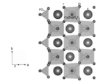
- FIG. 12 is a schematic diagram showing the crystal structure of the phosphor according to the present embodiment.
- the occupied position of the light emitting element Eu 2+ is the Ca site (see Table 1). Note that the crystal structure shown in FIG. 12 shows a case when viewed from the b-axis direction.
- FIG. 13 is a diagram for explaining a crystal structure of a light emitting site.
- the Eu 2+ site has an octahedral structure in which six anions are coordinated.
- the breakdown of anions is 4 oxygen ions and 2 fluorine ions.
- the structure of octahedral EuO 4 F 2 has a cis-type structure in which two fluorine ions are adjacent to each other.
- Fluoride ion octahedra EuO 4 F 2 is the b-axis direction of the crystal are aligned in a straight line, and connect the octahedral EuO 4 F 2 together in the form of corner sharing octahedra EuO 4 F 2.
- the octahedron EuO 4 F 2 is connected in a zigzag manner in the b-axis direction around the fluorine ion (see FIG. 14).
- Each oxygen ion of the octahedron EuO 4 F 2 shares a vertex with the PO 4 tetrahedron.
- FIG. 14 is a schematic view of the crystal structure of the phosphor shown in FIG. 12 viewed from another direction.
- octahedral EuO 4 F 2 is arranged in a staggered pattern by fluorine ions and PO 4 tetrahedron. Yes. Potassium ions are lined up so as to fill the space between the staggered lattices of octahedron EuO 4 F 2 .
- a perovskite structure represented by a composition formula ABX 3 is formed.
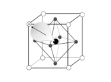
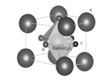
- FIG. 15 is a diagram showing a light emitting site having a perovskite crystal structure according to the present embodiment.
- the eight potassium ions are located at the apex of the cubic lattice (A site).
- Oxygen ions and fluorine ions as anions of the octahedral EuO 4 F 2 are located at the face center of the cubic lattice formed by potassium.
- Europium (or calcium) ions are located at the center of the cubic lattice (B site).
- the ionic radius of 1.51 ⁇ ⁇ ⁇ ⁇ of potassium ions (K + ) occupying the A site is 29% larger than the ionic radius of 1.17 ⁇ ⁇ ⁇ of europium ions (Eu 2+ ) occupying the B site.
- the electron density of cis-type octahedron EuO 4 F 2 centering on divalent europium ions is biased toward the fluorine side with high electronegativity. Therefore, since the symmetry of the octahedral electron distribution is lost, the degeneracy of the 5d orbit of the divalent europium ion can be solved. As a result, valence electrons in the inner shell 4f orbit of divalent europium are likely to transition to the d xz or d yz orbit of the 5d orbit even at low energy.
- the direction of the d xz or d yz orbit is the apex direction of the cubic lattice constituting the perovskite structure.
- the position is occupied by a cation K + having a large ion radius.
- an electrostatic attractive force is generated between the electron cloud of Eu 2+ 5d electrons (d xz or d yz orbit) and the cation K + .
- the mass of K + ions is large and difficult to move, the spread of the d xz or d yz orbital electron cloud increases.
- the existence probability of electrons in the d xz or d yz orbit is increased and the energy level is decreased, and thus a large Stokes shift is exhibited.
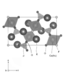
- FIG. 16 is a schematic view of the unit cell of the phosphor according to the present embodiment viewed from the a-axis.
- FIG. 17 is a schematic view of the unit cell of the phosphor according to the present embodiment as seen from the b-axis.
- FIG. 18 is a schematic view of the unit cell of the phosphor according to the present embodiment viewed from the c-axis.
- the unit cell includes atoms having the coordinates shown in Table 1.
- the a-axis corresponds to coordinates (x, 0, 0)
- the b-axis corresponds to (0, y, 0)
- the c-axis corresponds to (0, 0, z).
- FIG. 19 is a diagram illustrating an excitation spectrum and an emission spectrum of the phosphor according to Example 1.
- the excitation emission spectrum was measured at room temperature using a multichannel optical spectrometer (PMA C5966-31 (manufactured by Hamamatsu Photonics)).
- the emission spectrum was measured with 400 nm excitation.
- the excitation spectrum was measured by adjusting the monitor wavelength to the emission peak wavelength at 400 nm excitation.
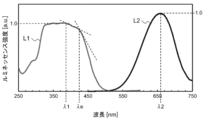
- the excitation spectrum L1 of the phosphor according to Example 1 has a peak wavelength ⁇ 1 in the range of 330 to 420 nm, more specifically in the range of 350 to 390 nm.
- the excitation end wavelength ⁇ e is about 420 nm, and the energy at that wavelength is 2.938 eV.
- the emission spectrum L2 has a peak wavelength ⁇ 2 of 658 nm, a full width at half maximum of 152 nm, and the energy of the peak wavelength ⁇ 2 is 1.884 eV. Therefore, the Stokes shift is 1.054 eV.
- the chromaticity coordinates (cx, cy) of the light emitted from this phosphor are (0.613, 0.384).
- Example 1 The powder sample obtained in Example 1 was embedded in a transparent resin, polished so that the measurement surface was flat, and then subjected to composition analysis using EPMA (manufactured by JEOL). As a result, it became clear that the composition ratio of the phosphor according to Example 1 was KF ⁇ Ca 0.99 KPO 4 : Eu 2+ 0.01 .
- FIG. 20 is a diagram showing temperature characteristics of phosphor emission according to Example 1.
- FIG. 17 shows the relative intensities at the respective temperatures normalized by setting the emission intensity at 30 ° C. excited with light having a wavelength of 400 nm as 100%.
- the emission intensity maintenance ratio was 90% or more compared to 30 ° C., and despite the large Stokes shift, good temperature characteristics could be confirmed.
- the anion with respect to the emission center Eu of the phosphor according to Example 1 has a cis-type octahedral structure of EuO 4 F 2 . That is, an anion is located in each crystal axis direction (see FIG. 6A).
- the phosphor according to the first embodiment is excited with energy as low as 3.10 eV (400 nm)
- the energy level of the t 2g orbit due to the crystal field splitting of the 5d orbit is lowered, and the 5d orbit is expanded in this direction.
- FIG. 21 is a schematic diagram showing the spread of an electron cloud in octahedron EuO 4 F 2 .
- the electrostatic attractive force of the cation at the apex position of the perovskite cube does not act on the 5d orbit extending in the axial direction. Instead, an electrostatic repulsive force (repulsive force) acts with the anion in the axial direction. Therefore, the spread of the 5d orbit is suppressed, and light emission is shifted to the light on the short wavelength side.
- FIG. 22 is a diagram showing an emission spectrum when the phosphor according to Example 1 is irradiated with high energy ultraviolet rays. As shown in FIG. 22, in the phosphor according to Example 1, blue-green light emission with a peak wavelength ⁇ 2 of the emission spectrum of 476 nm was confirmed.
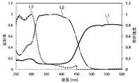
- FIG. 23 is a diagram showing a diffuse reflection spectrum of the phosphor according to Example 1.
- FIG. 23 As can be seen from the line L1 in FIG. 23, most of light of 420 nm or less is absorbed.
- the excitation spectrum L2 (monitor wavelength 622 nm) of red emission and the excitation spectrum (monitor wavelength 476 nm) L3 of blue-green emission are superimposed on this. From this, the excitation band of red emission is in the range of 330 to 420 nm, and the excitation band of blue-green emission can be confirmed in the vicinity of 250 to 320 nm. This indicates that one emission center changes the emission color due to the difference in excitation wavelength.
- the phosphor according to the present embodiment emits red light with light having the first wavelength (for example, near ultraviolet light or short wavelength visible light having a peak wavelength of 380 to 450 nm), and light having the first wavelength.
- the light of the second wavelength shorter than the second wavelength (for example, ultraviolet light having a wavelength of 200 to 350 nm) emits light having a wavelength shorter than the red color (for example, blue to green having a wavelength of 450 nm to 550 nm).
- Example 2 In the phosphor according to Example 2, the elements constituting the crystal structure ABX 3 of the light emitting site are as follows: cation A is K + (0.997) and Na + (0.003), cation B is Eu 2+ , and anion X is O 2- and F - a. Further, the cation M constituting the tetrahedron MO 4 that connects the perovskite structures of the light emitting sites is P 5+ .
- the phosphor according to Example 2 is manufactured by the following method. First, KF, NaF, and K 2 CO 3 powder are dried at 150 ° C. for 2 hours. Then, in a glove box filled with dry N 2 , KF, K 2 CO 3 , NaF, CaHPO 4 , (NH 3 ) 2 HPO 4 , Eu 2 O 3 are in a stoichiometric ratio of 0.994: 0.500: It precisely weighed so that it might become a ratio of 0.006: 0.960: 0.040: 0.020 (mol), and it pulverized and mixed in the alumina mortar, and obtained raw material mixed powder. Thereafter, the same processing as in Example 1 was performed to obtain a phosphor according to Example 2.
- Example 2 The powder sample obtained in Example 2 was subjected to composition analysis in the same manner as in Example 1. As a result, it became clear that the composition ratio of the phosphor according to Example 2 was (K 0.994 , Na 0.006 ) F ⁇ Ca 0.96 KPO 4 : Eu 2+ 0.04 .
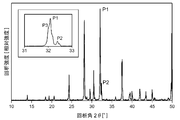
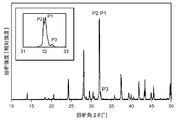
- FIG. 24 is a diagram showing an X-ray diffraction pattern of the phosphor according to Example 2. The measurement was performed at a sampling width of 0.02 ° and a scanning speed of 2.0 ° / min. Since P1, P2, and P3 are observed in an overlapping manner, a pattern in which that portion is enlarged is inserted in the figure. As a result, a diffraction pattern similar to that in Example 1 was obtained, and it was confirmed that the crystal structure was the same. Therefore, the occupied site of Eu is also the B site as in Example 1, and the coordination structure thereof has a perovskite structure. The average ionic radius of 1.51 ⁇ considering the occupancy of potassium and sodium occupying the A site is 29% larger than the ionic radius of 1.17 ⁇ of Eu 2+ occupying the B site.
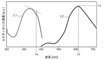
- FIG. 25 is a diagram showing an excitation spectrum and an emission spectrum of the phosphor according to Example 2. The excitation emission spectrum was measured by the same method as in Example 1.
- the excitation spectrum L1 of the phosphor according to Example 2 has a peak wavelength ⁇ 1 in the range of 330 to 420 nm, more specifically in the range of 350 to 390 nm.
- the wavelength ⁇ e at the excitation end is about 425 nm, and the energy at that wavelength is 2.917 eV.
- the peak wavelength ⁇ 2 is 658 nm, and the energy of the peak wavelength ⁇ 2 is 1.484 eV. Therefore, the Stokes shift is 1.033 eV.
- the chromaticity coordinates (cx, cy) of the light emitted from the phosphor are (0.553, 0.377).
- Example 3 In the phosphor according to Example 3, the elements constituting the crystal structure ABX 3 of the light emitting site are as follows: cation A is K + (0.997) and Rb + (0.003), cation B is Eu 2+ , and anion X is O 2- and F - a. Further, the cation M constituting the tetrahedron MO 4 that connects the perovskite structures of the light emitting sites is P 5+ .
- the phosphor according to Example 3 is manufactured by the following method. First, KF, RbF, and K 2 CO 3 powder are dried at 150 ° C. for 2 hours. Then, in a glove box filled with dry N 2 , KF, K 2 CO 3 , RbF, CaHPO 4 , (NH 3 ) 2 HPO 4 , and Eu 2 O 3 are in a stoichiometric ratio of 0.994: 0.600: It precisely weighed so that it might become a ratio of 0.005: 0.960: 0.040: 0.020 (mol), and it grind
- Example 3 The powder sample obtained in Example 3 was subjected to composition analysis in the same manner as in Example 1. As a result, it was revealed that the composition ratio of the phosphor according to Example 3 was (K 0.994 , Rb 0.006 ) F ⁇ Ca 0.96 KPO 4 : Eu 2+ 0.04 .
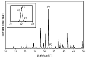
- FIG. 26 is a diagram showing an X-ray diffraction pattern of the phosphor according to Example 3. The measurement was performed under the same conditions as in Example 2. Since P1, P2, and P3 are observed in an overlapping manner, a pattern in which that portion is enlarged is inserted in the figure. As a result, a diffraction pattern similar to that of Example 1 was obtained, and it was confirmed that the crystal structure was the same. Therefore, the occupied site of Eu is also the B site as in Example 1, and the coordination structure thereof has a perovskite structure. The average ionic radius of 1.51 ⁇ considering the occupancy of potassium and rubidium occupying the A site is 29% larger than the ionic radius of 1.17 ⁇ of Eu 2+ occupying the B site.
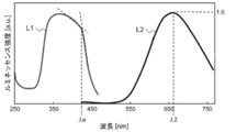
- FIG. 27 is a diagram showing an excitation spectrum and an emission spectrum of the phosphor according to Example 3. The excitation emission spectrum was measured by the same method as in Example 1.
- the excitation spectrum L1 of the phosphor according to Example 3 has a peak wavelength ⁇ 1 in the range of 330 to 420 nm, more specifically in the range of 350 to 390 nm.
- the wavelength ⁇ e at the excitation end is about 395 nm, and the energy at that wavelength is 3.139 eV.
- the peak wavelength ⁇ 2 is 654 nm, and the energy of the peak wavelength ⁇ 2 is 1.896 eV. Therefore, the Stokes shift is 1.243 eV.
- the chromaticity coordinates (cx, cy) of the light emitted from the phosphor are (0.583, 0.391).
- Example 4 In the phosphor according to Example 4, the elements constituting the crystal structure ABX 3 of the light emitting site are as follows: cation A is K + (0.95) and Li + (0.05), cation B is Eu 2+ , and anion X is O 2- and F - a. Further, the cation M constituting the tetrahedron MO 4 that connects the perovskite structures of the light emitting sites is P 5+ .
- the phosphor according to Example 4 is manufactured by the following method. First, KF, LiF, and K 2 CO 3 powder are dried at 150 ° C. for 2 hours. Then, in a glove box filled with dry N 2 , KF, K 2 CO 3 , LiF, CaHPO 4 , (NH 3 ) 2 HPO 4 , Eu 2 O 3 are in a stoichiometric ratio of 0.90: 0.500: It was precisely weighed so as to have a ratio of 0.10: 0.960: 0.040: 0.020 (mol), and pulverized and mixed in an alumina mortar to obtain a raw material mixed powder. Thereafter, the same processing as in Example 1 was performed to obtain the phosphor according to Example 4.
- Example 4 The powder sample obtained in Example 4 was subjected to composition analysis in the same manner as in Example 1. As a result, it became clear that the composition ratio of the phosphor according to Example 4 was (K 0.90 , Li 0.10 ) F ⁇ Ca 0.96 KPO 4 : Eu 2+ 0.04 .
- FIG. 28 is a diagram showing an X-ray diffraction pattern of the phosphor according to Example 4.
- the measurement was performed under the same conditions as in Example 2. Since P1, P2, and P3 are observed in an overlapping manner, a pattern in which that portion is enlarged is inserted in the figure. As a result, a diffraction pattern similar to that in Example 1 was obtained, and it was confirmed that the crystal structure was the same. Therefore, the occupied site of Eu is also the B site as in Example 1, and the coordination structure thereof has a perovskite structure.
- the average ionic radius of 1.48 ⁇ ⁇ taking into account the occupancy of potassium and lithium occupying the A site is 26% larger than the ionic radius of 1.17 ⁇ of Eu 2+ occupying the B site.
- FIG. 29 is a diagram showing an excitation spectrum and an emission spectrum of the phosphor according to Example 4.
- the excitation emission spectrum was measured by the same method as in Example 1.
- the excitation spectrum L1 of the phosphor according to Example 2 has a peak wavelength ⁇ 1 in the range of 330 to 420 nm, more specifically in the range of 350 to 390 nm.
- the wavelength ⁇ e at the excitation end is about 425 nm, and the energy at that wavelength is 2.917 eV.
- the peak wavelength ⁇ 2 is 659 nm, and the energy of the peak wavelength ⁇ 2 is 1.881 eV. Therefore, the Stokes shift is 1.036 eV.
- the chromaticity coordinates (cx, cy) of the light emitted from the phosphor are (0.511, 0.383).
- Example 5 In the phosphor according to Example 5, the elements constituting the crystal structure ABX 3 of the light emitting site are as follows: cation A is K + (0.95) and Ag + (0.05), cation B is Eu 2+ , and anion X is O 2- and F - a. Further, the cation M constituting the tetrahedron MO 4 that connects the perovskite structures of the light emitting sites is P 5+ .
- the phosphor according to Example 5 is manufactured by the following method. First, KF, AgF, and K 2 CO 3 powder are dried at 150 ° C. for 2 hours. Then, in a glove box filled with dry N 2 , KF, K 2 CO 3 , AgF, CaHPO 4 , (NH 3 ) 2 HPO 4 , and Eu 2 O 3 are in a stoichiometric ratio of 0.90: 0.500: It was precisely weighed so as to have a ratio of 0.10: 0.960: 0.040: 0.020 (mol), and pulverized and mixed in an alumina mortar to obtain a raw material mixed powder. Thereafter, the same processing as in Example 1 was performed to obtain the phosphor according to Example 5.
- Example 5 The powder sample obtained in Example 5 was subjected to composition analysis in the same manner as in Example 1. As a result, it was revealed that the composition ratio of the phosphor according to Example 5 was (K 0.90 , Ag 0.10 ) F ⁇ Ca 0.96 KPO 4 : Eu 2+ 0.04 .
- FIG. 30 is a diagram showing an X-ray diffraction pattern of the phosphor according to Example 5.
- FIG. The measurement was performed under the same conditions as in Example 2. Since P1, P2, and P3 are observed in an overlapping manner, a pattern in which that portion is enlarged is inserted in the figure. As a result, a diffraction pattern similar to that of Example 1 was obtained, and it was confirmed that the crystal structure was the same. Therefore, the occupied site of Eu is also the B site as in Example 1, and the coordination structure thereof has a perovskite structure.
- the average ionic radius of 1.50 ⁇ considering the occupation ratio of potassium and silver occupying the A site is 28% larger than the ionic radius of 1.171.1 of Eu 2+ occupying the B site.
- FIG. 31 is a diagram showing an excitation spectrum and an emission spectrum of the phosphor according to Example 5.
- the excitation emission spectrum was measured by the same method as in Example 1.
- the excitation spectrum L1 of the phosphor according to Example 5 has a peak wavelength ⁇ 1 in the range of 330 to 420 nm, more specifically in the range of 350 to 390 nm.
- the wavelength ⁇ e at the excitation end is about 423 nm, and the energy at that wavelength is 2.931 eV.
- the peak wavelength ⁇ 2 is 662 nm, and the energy of the peak wavelength ⁇ 2 is 1.873 eV. Therefore, the Stokes shift is 1.058 eV.
- the chromaticity coordinates (cx, cy) of the light emitted from the phosphor are (0.610, 0.374).
- Example 6 In the phosphor according to Example 6, the elements constituting the crystal structure ABX 3 of the light emitting site are as follows: cation A is K + , cation B is Eu 2+ (0.97) and Yb 2+ (0.03), and anion X is O 2- and F - a. Further, the cation M constituting the tetrahedron MO 4 that connects the perovskite structures of the light emitting sites is P 5+ .
- the phosphor according to Example 6 is manufactured by the following method. First, KF and K 2 CO 3 powder are dried at 150 ° C. for 2 hours. And in the glove box filled with dry N 2 , the stoichiometric ratio of KF, K 2 CO 3 , CaHPO 4 , (NH 3 ) 2 HPO 4 , Eu 2 O 3 , Yb 2 O 3 is 1.0000: 0. The powder was precisely weighed so as to have a ratio of 5000: 0.9700: 0.030: 0.0145: 0.0005 (mol), and pulverized and mixed in an alumina mortar to obtain a raw material mixed powder. Thereafter, the same processing as in Example 1 was performed to obtain the phosphor according to Example 6.
- Example 6 The powder sample obtained in Example 6 was subjected to composition analysis in the same manner as in Example 1. As a result, the composition ratio of the phosphor according to Example 6 was found to be KF ⁇ Ca 0.97 KPO 4 : Eu 2+ 0.029 , Yb 2+ 0.001 .
- FIG. 32 is a diagram showing an X-ray diffraction pattern of the phosphor according to Example 6. The measurement was performed under the same conditions as in Example 2. Since P1, P2, and P3 are observed in an overlapping manner, a pattern in which that portion is enlarged is inserted in the figure. As a result, a diffraction pattern similar to that in Example 1 was obtained, and it was confirmed that the crystal structure was the same. Therefore, the occupied site of Eu is also the B site as in Example 1, and the coordination structure thereof has a perovskite structure. The average ionic radius of 1.51 kg of potassium occupying the A site is 29% larger than the average ionic radius of 1.17 kg considering the occupancy of Eu 2+ and Yb 2+ occupying the B site.
- FIG. 33 is a diagram showing an excitation spectrum and an emission spectrum of the phosphor according to Example 6. The excitation emission spectrum was measured by the same method as in Example 1.
- the excitation spectrum L1 of the phosphor according to Example 6 has a peak wavelength ⁇ 1 in the range of 330 to 420 nm, more specifically in the range of 350 to 390 nm.
- the wavelength ⁇ e at the excitation end is about 421 nm, and the energy at that wavelength is 2.945 eV.
- the peak wavelength ⁇ 2 is 661 nm, and the energy of the peak wavelength ⁇ 2 is 1.876 eV. Therefore, the Stokes shift is 1.069 eV.
- the chromaticity coordinates (cx, cy) of the light emitted from the phosphor are (0.605, 0.380).
- Example 7 In the phosphor according to Example 7, the elements constituting the crystal structure ABX 3 of the light emitting site are as follows: cation A is K + , cation B is Eu 2+ (0.97) and Ce 3+ (0.03), and anion X is O 2- and F - a. Further, the cation M constituting the tetrahedron MO 4 that connects the perovskite structures of the light emitting sites is P 5+ .
- the phosphor according to Example 7 is manufactured by the following method. First, KF and K 2 CO 3 powder are dried at 150 ° C. for 2 hours. And in the glove box filled with dry N 2 , the stoichiometric ratio of KF, K 2 CO 3 , CaHPO 4 , (NH 3 ) 2 HPO 4 , Eu 2 O 3 , CeO 2 is 1.0000: 0.4995. : 0.9700: 0.0300: 0.0145: 0.001 (mol) and precisely weighed and pulverized and mixed in an alumina mortar to obtain a raw material mixed powder. Thereafter, the same processing as in Example 1 was performed to obtain the phosphor according to Example 7. The powder sample obtained in Example 7 was subjected to composition analysis in the same manner as in Example 1. As a result, it was revealed that the composition ratio of the phosphor according to Example 7 was KF ⁇ Ca 0.97 KPO 4 : Eu 2+ 0.029 , Ce 3+ 0.001 .
- Example 34 is a diagram showing an X-ray diffraction pattern of the phosphor according to Example 7.
- FIG. The measurement was performed under the same conditions as in Example 2. Since P1, P2, and P3 are observed in an overlapping manner, a pattern in which that portion is enlarged is inserted in the figure. As a result, a diffraction pattern similar to that in Example 1 was obtained, and it was confirmed that the crystal structure was the same. Therefore, the occupied site of Eu is also the B site as in Example 1, and the coordination structure thereof has a perovskite structure.
- the average ionic radius of 1.51 kg of potassium occupying the A site is 29% larger than the average ionic radius of 1.17 mm considering the occupancy of Eu 2+ and Ce 3+ occupying the B site.
- FIG. 35 is a diagram showing an excitation spectrum and an emission spectrum of the phosphor according to Example 7. The excitation emission spectrum was measured by the same method as in Example 1.
- the excitation spectrum L1 of the phosphor according to Example 7 has a peak wavelength ⁇ 1 in the range of 330 to 420 nm, more specifically in the range of 350 to 390 nm.
- the wavelength ⁇ e at the excitation end is about 418 nm, and the energy at that wavelength is 2.966 eV.
- the peak wavelength ⁇ 2 is 655 nm, and the energy of the peak wavelength ⁇ 2 is 1.893 eV. Therefore, the Stokes shift is 1.073 eV.
- the chromaticity coordinates (cx, cy) of the light emitted from this phosphor are (0.608, 0.380).
- Example 8 In the phosphor according to Example 8, the elements constituting the crystal structure ABX 3 of the light emitting site are as follows: cation A is K + , cation B is Eu 2+ , anion X is O 2 ⁇ and F ⁇ (0.995): Cl (0.005). Further, the cation M constituting the tetrahedron MO 4 that connects the perovskite structures of the light emitting sites is P 5+ .
- the phosphor according to Example 8 is manufactured by the following method. First, KF and K 2 CO 3 powder are dried at 150 ° C. for 2 hours. Then, in a glove box filled with dry N 2 , KF, K 2 CO 3 , KCl, CaHPO 4 , (NH 3 ) 2 HPO 4 , Eu 2 O 3 are in a stoichiometric ratio of 0.995: 0.500: It precisely weighed so that it might become a ratio of 0.005: 0.990: 0.010: 0.005 (mol), and it ground and mixed in the alumina mortar, and obtained raw material mixed powder. Thereafter, the same processing as in Example 1 was performed to obtain the phosphor according to Example 8.
- Example 8 The powder sample obtained in Example 8 was subjected to composition analysis in the same manner as in Example 1. As a result, it became clear that the composition ratio of the phosphor according to Example 8 was K (F 0.995 , Cl 0.005 ) ⁇ Ca 0.99 KPO 4 : Eu 2+ 0.01 .
- FIG. 36 is a diagram showing an X-ray diffraction pattern of the phosphor according to Example 8.
- FIG. The measurement was performed under the same conditions as in Example 2. Since P1, P2, and P3 are observed in an overlapping manner, a pattern in which that portion is enlarged is inserted in the figure. As a result, a diffraction pattern similar to that in Example 1 was obtained, and it was confirmed that the crystal structure was the same. Therefore, the occupied site of Eu is also the B site as in Example 1, and the coordination structure thereof has a perovskite structure.
- the ionic radius of 1.51 ⁇ ⁇ ⁇ of potassium occupying the A site is 29% larger than the ionic radius of 1.17 ⁇ of Eu 2+ occupying the B site.
- FIG. 37 is a diagram showing an excitation spectrum and an emission spectrum of the phosphor according to Example 8. The excitation emission spectrum was measured by the same method as in Example 1.
- the excitation spectrum L1 of the phosphor according to Example 8 has a peak wavelength ⁇ 1 in the range of 330 to 420 nm, more specifically in the range of 350 to 390 nm.
- the wavelength ⁇ e at the excitation end is about 414 nm, and the energy at that wavelength is 2.995 eV.
- the peak wavelength ⁇ 2 is 658 nm, and the energy of the peak wavelength ⁇ 2 is 1.484 eV. Therefore, the Stokes shift is 1.111 eV.
- the chromaticity coordinates (cx, cy) of the light emitted from the phosphor are (0.553, 0.378).
- Example 9 In the phosphor according to Example 9, the elements constituting the crystal structure ABX 3 of the light emitting site are K + for the cation A, Eu 2+ for the cation B, and O 2 ⁇ and F ⁇ for the anion X.
- the cations M constituting the tetrahedron MO 4 that connects the perovskite structures of the light emitting sites are P 5+ (0.999) and V 5+ (0.001).
- the phosphor according to Example 9 is manufactured by the following method. First, KF and K 2 CO 3 powder are dried at 150 ° C. for 2 hours. Then, in a glove box filled with dry N 2 , KF, K 2 CO 3 , CaHPO 4 , V 2 O 5 , (NH 3 ) 2 HPO 4 , Eu 2 O 3 are stoichiometrically 1.000: 0. .500: 0.980: 0.001: 0.018: 0.010 (mol) and precisely weighed and pulverized and mixed in an alumina mortar to obtain a raw material mixed powder. Thereafter, the same processing as in Example 1 was performed to obtain the phosphor according to Example 9.
- Example 9 The powder sample obtained in Example 9 was subjected to composition analysis in the same manner as in Example 1. As a result, it became clear that the composition ratio of the phosphor according to Example 9 was KF ⁇ Ca 0.98 K (P 0.999 , V 0.001 ) O 4 : Eu 2+ 0.02 .
- FIG. 38 is a diagram showing an X-ray diffraction pattern of the phosphor according to Example 9. The measurement was performed under the same conditions as in Example 2. Since P1, P2, and P3 are observed in an overlapping manner, a pattern in which that portion is enlarged is inserted in the figure. As a result, a diffraction pattern similar to that in Example 1 was obtained, and it was confirmed that the crystal structure was the same. Therefore, the occupied site of Eu is also the B site as in Example 1, and the coordination structure thereof has a perovskite structure. The ionic radius of 1.51 ⁇ ⁇ ⁇ of potassium occupying the A site is larger than the ionic radius of 1.17 ⁇ of Eu 2+ occupying the B site.
- FIG. 39 is a diagram showing an excitation spectrum and an emission spectrum of the phosphor according to Example 9. The excitation emission spectrum was measured by the same method as in Example 1.
- the excitation spectrum L1 of the phosphor according to Example 9 has a peak wavelength ⁇ 1 in the range of 330 to 420 nm, more specifically in the range of 350 to 390 nm.
- the wavelength ⁇ e at the excitation end is about 426 nm, and the energy at that wavelength is 2.910 eV.
- the peak wavelength ⁇ 2 is 658 nm, and the energy of the peak wavelength ⁇ 2 is 1.484 eV. Therefore, the Stokes shift is 1.034 eV.
- the chromaticity coordinates (cx, cy) of the light emitted from this phosphor are (0.555, 0.372).
- the present invention can be used for light sources and lamps.
Landscapes
- Chemical & Material Sciences (AREA)
- Organic Chemistry (AREA)
- Inorganic Chemistry (AREA)
- Engineering & Computer Science (AREA)
- Materials Engineering (AREA)
- Luminescent Compositions (AREA)
Abstract
ある態様の蛍光体は、発光サイトがABX3(A,Bはカチオン、Xはアニオン)で表されるペロブスカイト結晶構造を持ち、該ペロブスカイト結晶構造の体心となるBサイトに発光元素が位置している。
Description
本発明は、蛍光体に関する。
近年、蛍光灯や白熱電球の代替光源として白色発光ダイオード(LED)が普及してきている。このような白色LEDにおいても、従来の光源と同様に自然光に近い高い演色性が求められている。現在主流の白色LEDは、青色発光の半導体発光素子と黄色蛍光体とを組み合わせたものが一般的である。
しかしながら、青色光と黄色光とを合成した疑似白色では赤色成分が不足となるため、高い演色性を実現することは困難であった。そこで、高い演色性を実現すべく、赤色成分を補う赤色蛍光体を黄色蛍光体(又は緑色蛍光体)と組み合わせた混合蛍光体を用いた白色LEDも考案されている。
従来、様々な赤色蛍光体が開発されているが、例えば、CaAlSiN3:Eu、(Ca,Sr)AlSiN3:Eu、Ca2Si5N8:Euといった組成の赤色蛍光体が開発されている(特許文献1~3参照)。
しかしながら、従来の赤色蛍光体は、上述の組成の蛍光体を含め窒化物が主流である。窒化物の蛍光体の合成には、脱酸素雰囲気、高温高圧等の特殊な環境が必要であり、製造コストの増大を招いている。
また、上述の赤色蛍光体は、励起端が500~550nmの間にある。そのため、このような赤色蛍光体を、白色光を実現するために他の色で発光する蛍光体と一緒に用いる場合、青色、緑色、黄色等の蛍光体が発する光を吸収して赤色に変換してしまう。その結果、蛍光体の含有量や塗布形態のわずかな変動に対して、所望の発光色から色度が大きくずれるといったことが生じ得るため、色調整が難しい。また、発光効率の低下を引き起こすことにもなる。
本発明はこうした状況に鑑みてなされたものであり、その目的とするところは、新規な蛍光体を提供することにある。
上記課題を解決するために、本発明のある態様の蛍光体は、発光サイトがABX3(A,Bはカチオン、Xはアニオン)で表されるペロブスカイト結晶構造を持ち、該ペロブスカイト結晶構造の体心となるBサイトに発光元素が位置している。
この態様によると、発光サイトがペロブスカイト結晶構造の新規な蛍光体を実現できる。
Xは、2種以上のアニオンで構成されていてもよい。これにより、カチオンBとアニオンXとからなるBX6八面体の結合に係わる電子密度を不均一にできる。その結果、結晶場分裂が大きくなり、比較的低エネルギの光で励起され発光する蛍光体を実現できる。
アニオンは、酸素、ハロゲン及び窒素からなる群から選択される2種以上の元素で構成されていてもよい。
アニオンは、酸素およびフッ素で構成されていてもよい。
Bは、Eu2+、Ce3+、Sm2+及びYb2+からなる群より選択される1種以上のカチオンであってもよい。これにより、4f-5d遷移が容易となる。
ペロブスカイト結晶構造のAサイトに位置するカチオンのイオン半径IAは、Bサイトに位置するカチオンのイオン半径IBよりも大きい。これにより、大きなストークスシフトを有する蛍光体を実現できる。
ペロブスカイト結晶構造のXサイトに位置するアニオンとしての酸素と、MO4(Mは、3~5価の金属元素)四面体構造の酸素とが共有されていてもよい。
以上の構成要素の任意の組合せ、本発明の表現を製造方法、灯具や照明などの装置、発光モジュール、光源などの間で変換したものもまた、本発明の態様として有効である。
本発明によれば、新規な蛍光体を提供できる。
以下、本発明を好適な実施の形態をもとに図面を参照しながら説明する。各図面に示される同一または同等の構成要素、部材、処理には、同一の符号を付するものとし、適宜重複した説明は省略する。また、実施の形態は、発明を限定するものではなく例示であって、実施の形態に記述されるすべての特徴やその組合せは、必ずしも発明の本質的なものであるとは限らない。
本実施の形態に係る蛍光体は、紫外線または短波長可視光で効率良く励起され発光する蛍光体である。具体的には、420nm以下の近紫外光または短波長可視光で強い励起を示し、発光スペクトルのピーク波長が600nm以上の赤色光を発する蛍光体である。また、本実施の形態に係る蛍光体は、ハロ酸化物の母体結晶にEu2+イオン等の賦活剤をドープすることで赤色発光を実現している。
また、本実施の形態に係る蛍光体は、ストークスシフトが大きい(0.8~1.2eV程度)赤色蛍光体である。そのため、青色、緑色、黄色等の他の蛍光体が発する可視光が吸収されにくい。なお、ストークスシフトとは、励起端波長と発光スペクトルのピーク波長とのエネルギ差をいう。ここで、励起端波長とは、励起スペクトルにおける長波長側の励起強度の低下が急減し始める波長を示している。
はじめに、本願発明に想到するまでの経緯について説明する。励起光密度の高い半導体発光素子の光に対応する蛍光体は、速い励起-発光のサイクルが必要となる。そのためには、電子スピン状態を維持したまま遷移できる4f-5d許容遷移が好適である。
4f-5d遷移が可能な元素は、Eu2+、Ce3+、Sm2+、Yb2+の希土類元素等が挙げられる。それらの希土類元素の外殻軌道は6sであり、その内殻に4f軌道がある。4f-5d遷移では、4f軌道の電子が外殻に位置する5d軌道に遷移することで、励起状態を形成する。このとき、5d軌道の電子雲の広がりが大きいほど、この軌道のエネルギレベルが下がり、遷移確率が高くなる。
図1は、結晶の状態に応じた励起及び発光のメカニズムを説明するための図である。低エネルギで励起するには、複雑な(あるいは歪んだ対称性の低い構造の)発光サイト構造か、共有結合性が必要である。
例えば、自由イオンでの4f-5d遷移には4.0eV以上のエネルギが必要である。その場合、波長が380~450nm程度の近紫外線または短波長可視光を発する半導体発光素子の光では遷移が発生しない。そこで、4f-5d遷移エネルギを下げるには、結晶中にドープし、希土類イオンの周りにアニオンを配位させることが有効である。5d軌道は、アニオンの配位により、2つの作用(重心シフトEc,結晶場分裂Ecfs)で低エネルギ化する。
重心シフトEcは、希土類元素(カチオン)にアニオンが配位することで、周りの負電荷の影響により、5つの5d軌道全体が低エネルギ化する。その効果は、配位するアニオンがイオン結合性の場合は小さく、共有結合性が増すと大きくなる。
イオン結合性の場合、結合に寄与する価電子はアニオン側に分布する。5d軌道に励起した電子は、マイナスチャージのアニオンと電気的反発が大きく、5d軌道の電子雲の広がり(遷移エネルギレベルの低下)は限定的になる。
共有結合性の場合、結合に寄与する価電子はアニオンとカチオンが共有する。共有結合性のアニオンのマイナスチャージは、イオン結合性のマイナスチャージより小さい。したがって、5d軌道に励起した電子の静電反発は小さくなり、5d軌道の電子雲は、大きく広がり、有効的な遷移エネルギの低下が起こる。つまり、重心シフトを大きくするには、共有結合性を高めることが重要であることがわかる。
結晶場分裂Ecfsは、希土類元素(カチオン)にアニオンが配位した立体構造により、5つある5d軌道の縮退が解け、5d軌道のエネルギレベル(軌道準位)が分裂することである。アニオンがない方向の5d軌道は、アニオンとの静電反発は小さく、5d軌道の電子雲は広がりやすい(エネルギレベルが低くなる)。一方、アニオンが配位している方向は、静電反発が大きくなり、エネルギレベルが高くなる。つまり、5d軌道の縮退を大きく分裂させるためには、歪んだ配位子場が必要になる。
図2は、窒化物を母体とする一般的な赤色蛍光体の励起スペクトルおよび発光スペクトルの一例を示す図である。近年普及している赤色蛍光体は、CaAlSiN3:Eu、Ca2Si5N8:Eu等の窒化物を母体とする蛍光体である。これらの蛍光体は、共有結合性を高めることで、重心シフトを大きくしているため、図2に示すように、励起帯(励起スペクトル)は長波長側まで広がっており、紫外領域の光だけでなく青色、緑色、黄色の可視光まで吸収してしまう。
図3は、ストークスシフトを説明するための模式図である。ストークスシフトは、励起状態での結晶構造の緩和によって起こる。蛍光体が基底状態4fから励起状態5dに励起されたとき、励起した電子軌道は配位アニオンに近づく。このとき、静電反発により、カチオン(希土類)に比べ軽い(原子量が小さい)アニオンの位置がずれる。しかし、アニオンの周りには元々他のカチオンが存在するため、平衡位置までの移動となる。このようなアニオンの移動により、励起状態の結晶構造は、基底状態とは異なってくる。この励起状態での結晶構造変化(緩和1)が起こった後に、基底状態に戻り、それに伴い発光が起こる。
カチオンである発光元素は、図3に示すように、基底状態から励起されて励起状態となり、励起状態での結晶構造変化(緩和)後に発光する。この際、エネルギ状態が変化する。この変化は、一般には配位座標で表される。図4は、配位座標を示す模式図である。配位座標の縦軸は、発光元素の価電子のエネルギレベル、横軸は、結晶の基底状態で最もエネルギレベルが下がる発光元素-アニオン間の距離をゼロとし、その変位を示す。
発光元素の4f電子は、励起光を吸収した瞬間に、エネルギレベルが上がり、励起状態になる。励起状態では、配位アニオンとの静電反発を解消する緩和が起こり、平衡状態までエネルギレベルが下がる。その時点から発光が始まるため、励起エネルギより小さなエネルギの遷移、長波長シフトが起こる。このとき、考慮しなければならないのはフォノン振動である。変位が大きくなれば、フォノン振動が大きくなる。その場合、系のエネルギレベルが上昇する。また、温度が上昇し、励起状態でのフォノン振動により基底状態の振動レベルと等しくなると、非輻射遷移となる。一般にストークスシフトが大きくなると温度特性の低下が懸念されていた。
本願発明者らは、上記の知見や考察に基づいて、ストークスシフトを増大させる新しい結晶構造を有する蛍光体の可能性に想到した。
蛍光体の励起/発光は、発光中心元素内の電子軌道遷移によって起こる。そのため、白色LEDのような高輝度光源における蛍光体には、遷移速度の速い4f-5d遷移をする発光元素(例えば、Eu2+、Ce3+)が望ましい。4f-5d遷移の励起は、6s軌道の内殻にある4f軌道の電子が励起エネルギを吸収し、6s軌道の外殻に広がる5d軌道に遷移する。発光は、5d軌道から4f軌道に戻ることで起こる。そのため、大きなストークスシフトを示すには、励起状態での5d軌道の広がりが大きくなることが重要となる。5d軌道の広がりは、発光元素周りの結晶構造によって決まる。そこで、本願発明者らは、5d軌道の広がりを大きくする結晶構造を考案した。
はじめに、本実施の形態に係る蛍光体が有する結晶構造の一つとして、ペロブスカイト結晶構造に着目した。図5は、ペロブスカイト結晶構造を示す図である。
組成式ABX3で表されるペロブスカイト結晶は、理想的には、立方晶系の単位格子をもち、立方晶の各頂点(Aサイト)に金属Aが、体心サイト(Bサイト)に金属Bが、立方晶の各面心サイト(Xサイト)にアニオンXが配置されている。また、金属Bには6つのアニオンXが配位し、BX6八面体を形成している。また、本実施の形態に係る発光サイトでは、Bサイトに4f-5d遷移する発光元素が位置している。このように、本実施の形態に係る蛍光体は、発光サイトがペロブスカイト結晶構造の新規な蛍光体である。
BX6八面体を形成しているアニオンXは、2種類以上のアニオンからなっていてもよい。具体的には、アニオンXの一つは酸素である。また、他の一種のアニオンXは、ハロゲンである。ハロゲンの中では、特にフッ素が好ましい。また、別の形態としては、酸素以外のもう一種のアニオンXが窒素であってもよい。
本実施の形態に係るAサイトは、イオン半径の大きな1価または2価のカチオンが占有している。Aサイトに位置するカチオンのイオン半径IAは、Bサイトに位置する発光元素のイオン半径IBより大きい。また、イオン半径IAはイオン半径IBより10%以上大きくてもよい。なお、Aサイトを占有するカチオンは、1価のカチオンからなる場合、2価のカチオンからなる場合、または、その両者からなる場合が有り得る。このように構成された本実施の形態に係る蛍光体は、低エネルギでの励起が可能であり、ストークスシフトも大きくなっている。
図6(a)は、6配位のBX6八面体の模式的に示す図、図6(b)は、6配位における5d軌道のエネルギ状態を説明するための図である。低エネルギ励起のメカニズムにおいては、前述の6配位のBX6八面体の対称性を低下させるミックスリガンド(複数種の配位子)を有することが好ましい。一般のペロブスカイト構造はABO3で表され、Bサイトには6つの酸素イオンが配位している。したがって、Bサイトは、イオン結合性が強く、また、対称性が高く、配位子場の歪が少ない。そのため、白色LEDに用いられる半導体発光素子の波長(380~450nm)の光のような小さなエネルギでは励起が難しい。
そこで、本実施の形態に係る蛍光体は、発光サイトのBサイトに2種以上のアニオンXを配位させることで、BX6八面体の結合に係わる電子密度を不均一にした。その結果、結晶場分裂が大きくなり、白色LEDに用いられるの半導体発光素子の発光(低エネルギ)で励起されるエネルギレベルまで励起帯が下がってくる。このとき5d軌道の縮退は、軸方向にあるアニオンXとの静電反発を避けるように広がるため、eg軌道よりt2g軌道のエネルギレベルが下がる。t2g軌道の中でも、アニオンXの密度が低いdxz、dyz方向のエネルギレベルが下がる。
図7は、分裂した軌道の広がりを模式的に示した図である。図7に示すように、分裂したdxz、dyz軌道は、立方晶の各頂点に位置するAサイト方向に広がる。Aサイトのカチオンは正電荷にチャージしている。Bサイトから広がってきたdxz、dyz軌道の電子はAサイトに引き付けられる(Aサイトのカチオンは、イオン半径が大きく質量が大きいため、静電引力によって引き付けられない。)。
dxz、dyz軌道の電子雲が静電引力によって大きく広がるため、dxz、dyz軌道のエネルギレベルは励起状態で低下する。そのため、ストークスシフトは大きくなる。通常の励起状態の緩和は、5d電子とアニオンの静電斥力によりアニオンの配位位置が変わり、配位子場の構造が大きく変化することで生じると考えられる。これに対して、本考案の結晶構造は5d電子とカチオンの静電引力により5d軌道を広げることから、配位子場の構造変化は少ない。このことは、カチオンの原子量が大きく重いため、動きづらいことが理由である。よって、本実施の形態に係る蛍光体は、ストークスシフトが大きいにも関わらず、安定した温度特性を示す。
本実施の形態に係る第1の蛍光体(例えば、赤色蛍光体)と、第1の蛍光体と異なる色の蛍光を発する第2の蛍光体(例えば、青色蛍光体、緑色蛍光体、黄色蛍光体、橙蛍光体等)と、第1の蛍光体および第2の蛍光体を励起する光を発する半導体発光素子と、を備えた発光モジュールは、以下の効果を奏する。
第1に、本実施の形態に係る第1の蛍光体の吸収が、半導体発光素子の発光波長より長い波長域においてほとんどないため、他の発光色の第2の蛍光体と混合した時に、色ずれを起こしにくくなる。第2に、本実施の形態に係る第1の蛍光体は、アニオンの移動による励起状態の緩和を起こさないため、励起による結晶構造変化が少なく、ストークスシフトが大きいにも関わらず、温度特性が良好となる。
(実施例1)
実施例1に係る蛍光体において、発光サイトの結晶構造ABX3を構成する元素は、
カチオンAがK+、カチオンBがEu2+、アニオンXがO2-及びF-である。なお、Eu2+以外にカチオンBとしてCe3+、Sm2+、Yb2+等を添加してもよい。これにより、4f-5d遷移が容易となる。また、発光サイトのペロブスカイト構造同士をつなぐ四面体MO4を構成するカチオンMはP5+である。なお、Mは、3~5価の金属元素であってもよい。
実施例1に係る蛍光体において、発光サイトの結晶構造ABX3を構成する元素は、
カチオンAがK+、カチオンBがEu2+、アニオンXがO2-及びF-である。なお、Eu2+以外にカチオンBとしてCe3+、Sm2+、Yb2+等を添加してもよい。これにより、4f-5d遷移が容易となる。また、発光サイトのペロブスカイト構造同士をつなぐ四面体MO4を構成するカチオンMはP5+である。なお、Mは、3~5価の金属元素であってもよい。
実施例1に係る蛍光体は以下の方法で製造される。はじめに、KF、K2CO3粉末を150℃、2時間乾燥する。そして、乾燥N2を充填したグローブボックス内で、KF、K2CO3、CaHPO4、(NH3)2HPO4、Eu2O3を化学量論比1.000:0.500:0.990:0.010:0.0050(mol)の割合となるように精秤し、アルミナ乳鉢中で粉砕混合し、原料混合粉末を得た。この原料混合粉末をアルミナ坩堝に入れ、1000℃で6時間焼成し、焼成粉末を得た。焼成する際の雰囲気は、N2/H2=95/5の混合ガス雰囲気である。そして、得られた焼成粉末を純水で洗浄し、実施例1に係る蛍光体を得た。
[X線回折パターン]
次に、X線回折測定について説明する。まず、粉末X線回折装置(RINT UltimaIII:Rigaku製)により、CuのKα線を発するX線管球を用い、サンプリング幅0.01°、スキャンスピード0.05°/minの条件で粉末X線回折測定を行った。図8は、実施例1に係る蛍光体のX線回折パターンを示す図である。
次に、X線回折測定について説明する。まず、粉末X線回折装置(RINT UltimaIII:Rigaku製)により、CuのKα線を発するX線管球を用い、サンプリング幅0.01°、スキャンスピード0.05°/minの条件で粉末X線回折測定を行った。図8は、実施例1に係る蛍光体のX線回折パターンを示す図である。
図8に示すように、実施例1に係る蛍光体に含まれる結晶の少なくとも一部が、CuのKα特性X線を用いたX線回折パターンにおいて、回折角2θが31.0°~33.0°の範囲に第1回折ピークP1、第2回折ピークP2及び第3回折ピークP3が存在し、最も強度の高い第1回折ピークP1の回折強度を100とした場合に、第2回折ピークP2および第3回折ピークP3の回折強度は30~50である。また、回折角2θが27.0°~29.0°の範囲に回折強度が15~25の第4回折ピークP4を有している。また、回折角2θが41.0°~43.0°の範囲に回折強度が15~25の第5回折ピークP5を有している。また、回折角2θが29.0°~31.0°の範囲に回折強度が10~15の第6回折ピークP6を有している。また、回折角2θが36.0°~39.0°の範囲に回折強度が10~15の第7回折ピークP7を有している。また、回折角2θが13.0°~15.0°の範囲に回折強度が5~10の第8回折ピークP8を有している。
また、実施例1に係る蛍光体の粉末サンプルについて、測定により得られたX線回折パターンから、データ処理ソフト(Rapid Auto:Rigaku製)を用い、本実施の形態に係る蛍光体の結晶系、ブラベ格子、空間群、及び格子定数を以下の通り決定した。
結晶系:単斜晶
ブラベ格子:単純格子
空間群:P21/m
格子定数:
a=7.3161(4)Å
b=5.8560(6)Å
c=12.6434(1)Å
α=γ=90°
β=90.3200°
V=541.673782Å3
結晶系:単斜晶
ブラベ格子:単純格子
空間群:P21/m
格子定数:
a=7.3161(4)Å
b=5.8560(6)Å
c=12.6434(1)Å
α=γ=90°
β=90.3200°
V=541.673782Å3
その後、結晶構造解析ソフトを用い、原子座標を決定した。上記解析の結果、前述の結晶は、X線回折に広く用いられるX線回折データベースであるICDD(International Center for Diffraction Date)に登録されていない新規構造の結晶であることが判明した。
なお、実施1の蛍光体は、アニオンに酸素とフッ素を含む。酸素とフッ素は周期表で隣り合わせの元素であり、X線回折のデータからだけではその占有位置を特定することは困難である。
そこで、Fの占有位置を把握するために、実施例1に係るサンプルの固体NMR測定を行った。固体NMRでは、スピン量子数が1/2の元素の結合状態が把握でき、19Fと31Pの結合関係を調べられる。測定は、磁場強度11.7T(500MHz)のJNM-ECZ500R(日本電子製)を用い行った。3.2mmの測定プローブに約50μLのサンプルを詰め、室温(約23℃)で測定した。
はじめに31PのDD-MAS(Dipolar Decoupling - Magic Angle Spinning)測定を行った。図9は、デカップリングなしで計測した共鳴スペクトルの結果を示す図である。図9に示すように、0.64ppmと0.76ppmに共鳴スペクトルを確認した。次に、19Fの磁気回転比に相当するラジオ波(470.6MHz)を照射し、P-Fの相互作用を消去してデカップリング測定した。図10は、P-Fの相互作用を消去してデカップリング測定した共鳴スペクトルの結果を示す図である。図10に示すように、共鳴スペクトルは1本のブロードな信号に変わった。この結果は、Pの原子振動にFが何らかの干渉をしていることを示しているが、カップリングの有無の判断に至らなかった。
次に、31P{19F}CP-CPMAS(Cross Polarization - Magic Angle Spinning)測定を行った。接触時間は50~20000μsで可変して計測した。図11は、31P{19F}CP-CPMAS測定の結果を示す図である。図11に示すように、接触時間を20000μsまで伸ばしても信号強度の極大値が現れず、接触時間の経過とともに単調に信号強度が増加した。このことから、フッ素はリンの近傍にあるが、フッ素とリンが直接結合していないことがわかる。
リンはテトラゴナルな配位構造を取りやすい。前述の固体NMRの結果から、リンには4つの酸素が配位していると判断した。そこで、実施例1のX線回折データを基に行う構造解析では、(PO4)3-の形で結晶中に存在するとして構造解析を行った。
各元素と原子座標との関係を表1に示す。
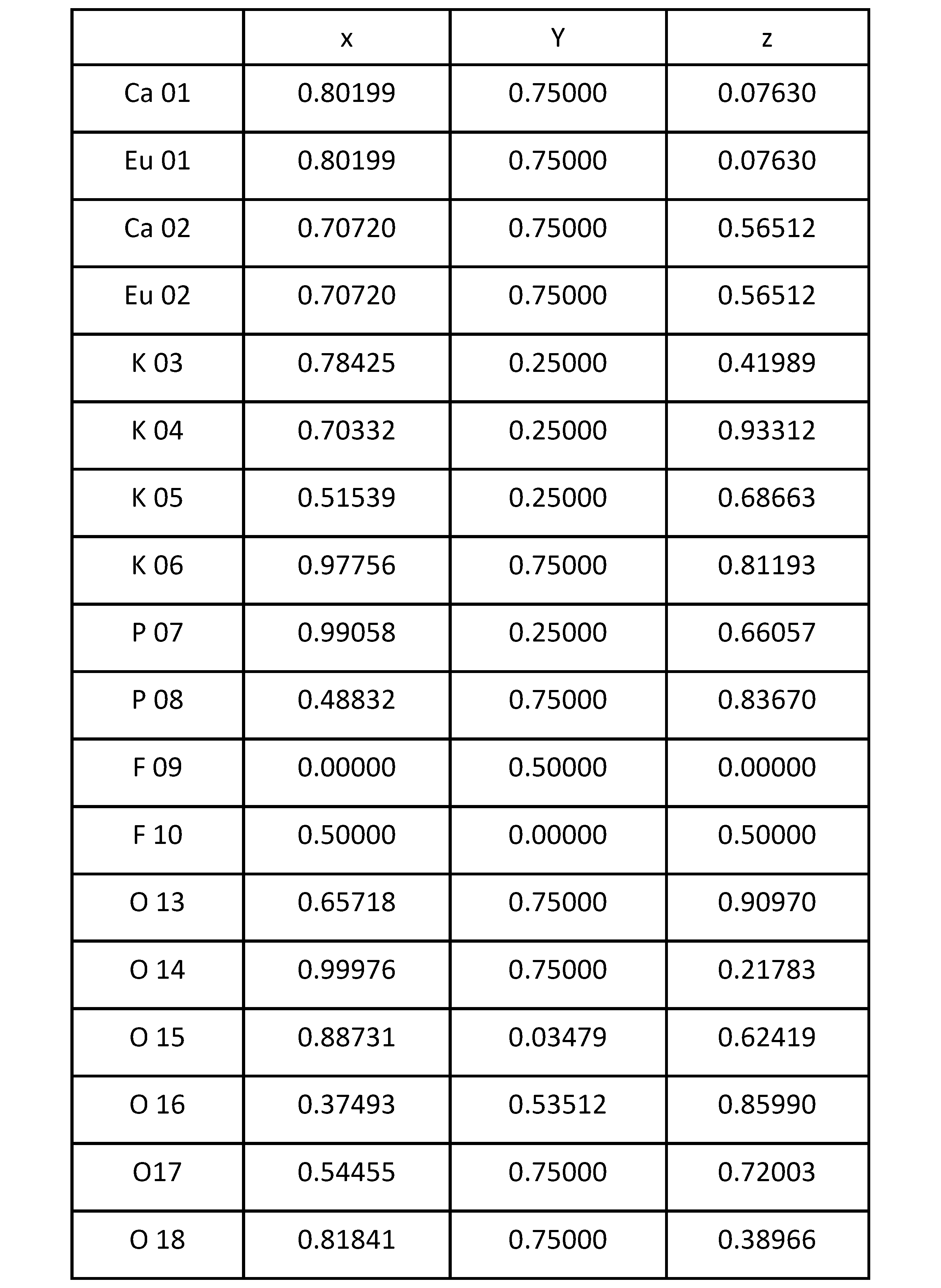
また、結晶構造解析の結果を図12に示す。図12は、本実施の形態に係る蛍光体の結晶構造を示す模式図である。発光元素Eu2+の占有位置はCaサイトになる(表1参照)。なお、図12に示す結晶構造は、b軸方向から見た場合を示している。
図13は、発光サイトが有する結晶構造を説明するための図である。Eu2+サイトは、6個のアニオンが配位した八面体構造をしている。アニオンの内訳は、酸素イオン4個とフッ素イオン2個である。八面体EuO4F2の構造は、2つのフッ素イオンが互いに隣接した位置をとるcis型構造をしている。
八面体EuO4F2のフッ素イオンは、本結晶のb軸方向に直線状に並んでおり、八面体EuO4F2の頂点を共有する形で八面体EuO4F2同士をつなげている。その結果、八面体EuO4F2は、フッ素イオンを中心にb軸方向にジグザグにつながっている(図14参照)。八面体EuO4F2の各酸素イオンは、PO4四面体と頂点を共有している。
図14は、図12に示す蛍光体の結晶構造を他の方向から見た模式図である。図14に示すように、b軸を中心にc軸を30°回転させた方向から結晶をみると、フッ素イオンとPO4四面体によって、八面体EuO4F2が千鳥格子状に並んでいる。カリウムイオンは、八面体EuO4F2の千鳥格子の間を埋めるように並んでいる。カリウムイオンと八面体EuO4F2の関係に着目すると組成式ABX3で表されるペロブスカイト構造をしている。
図15は、本実施の形態に係るペロブスカイト結晶構造の発光サイトを示す図である。図15に示すように、8個のカリウムイオンは、立方格子の頂点部に位置する(Aサイト)。八面体EuO4F2のアニオンとしての酸素イオンおよびフッ素イオンは、カリウムが構成する立方格子の面心に位置する。そして、ユーロピウム(またはカルシウム)イオンは、立方格子の体心に位置する(Bサイト)。Aサイトを占めるカリウムイオン(K+)のイオン半径1.51Åは、Bサイトを占めるユーロピウムイオン(Eu2+)のイオン半径1.17Åに対し29%大きい。
2価のユーロピウムイオンを中心としたcis型八面体EuO4F2の電子密度は、電気陰性度の高いフッ素側に偏る。そのため、八面体の電子分布の対称性は崩れるため、2価ユーロピウムイオンの5d軌道の縮退が解ける。その結果、2価ユーロピウムの内殻4f軌道にある価電子は、低いエネルギでも5d軌道のdxzまたはdyz軌道に遷移しやすくなる。dxzまたはdyz軌道の方向は、ペロブスカイト構造を構成する立方格子の頂点方向になる。その位置には、イオン半径の大きなカチオンK+が占有している。その結果、Eu2+の5d電子(dxzまたはdyz軌道)の電子雲とカチオンK+の間に静電引力が生じる。このとき、K+イオンは質量が大きく動きにくいため、dxzまたはdyz軌道電子雲の広がりが大きくなる。その結果、dxzまたはdyz軌道の電子の存在確率は高くなり、エネルギレベルが下がるため、大きなストークスシフトを示す。
[単位格子]
図12や図14に示す結晶構造の単位格子を以下に示す。図16は、本実施の形態に係る蛍光体の単位格子をa軸から見た模式図である。図17は、本実施の形態に係る蛍光体の単位格子をb軸から見た模式図である。図18は、本実施の形態に係る蛍光体の単位格子をc軸から見た模式図である。単位格子には、表1に示した座標の原子が含まれている。なお、a軸は座標(x,0,0)、b軸は(0,y,0)、c軸は(0,0,z)に対応する。
図12や図14に示す結晶構造の単位格子を以下に示す。図16は、本実施の形態に係る蛍光体の単位格子をa軸から見た模式図である。図17は、本実施の形態に係る蛍光体の単位格子をb軸から見た模式図である。図18は、本実施の形態に係る蛍光体の単位格子をc軸から見た模式図である。単位格子には、表1に示した座標の原子が含まれている。なお、a軸は座標(x,0,0)、b軸は(0,y,0)、c軸は(0,0,z)に対応する。
[励起スペクトルおよび発光スペクトル]
図19は、実施例1に係る蛍光体の励起スペクトルおよび発光スペクトルを示す図である。励起発光スペクトルの測定は、マルチチャンネル光学分光器(PMA C5966-31(浜松ホトニクス製))を用いて室温で行った。発光スペクトルは400nm励起で測定した。励起スペクトルは、モニタ波長を400nm励起時の発光ピーク波長に合わせ、測定した。
図19は、実施例1に係る蛍光体の励起スペクトルおよび発光スペクトルを示す図である。励起発光スペクトルの測定は、マルチチャンネル光学分光器(PMA C5966-31(浜松ホトニクス製))を用いて室温で行った。発光スペクトルは400nm励起で測定した。励起スペクトルは、モニタ波長を400nm励起時の発光ピーク波長に合わせ、測定した。
図19に示すように、実施例1に係る蛍光体の励起スペクトルL1は、ピーク波長λ1が330~420nmの範囲、より詳述すると350~390nmの範囲にある。また、励起端波長λeは420nm程度であり、その波長のエネルギは2.938eVである。一方、発光スペクトルL2は、ピーク波長λ2が658nmであり、半値幅が152nmであり、ピーク波長λ2のエネルギは1.884eVである。したがって、ストークスシフトは、1.054eVである。また、この蛍光体が発する光の色度座標(cx、cy)は、(0.613,0.384)である。
実施例1で得られた紛体サンプルを透明樹脂中に埋め込み、測定面が平坦になるように研磨後、EPMA(日本電子製)を用いて組成分析を行った。その結果、実施例1に係る蛍光体の組成比は、KF・Ca0.99KPO4:Eu2+
0.01であることが明らかになった。
図20は、実施例1に係る蛍光体発光の温度特性を示す図である。図17は、波長が400nmの光で励起した30℃の発光強度を100%として規格化した各温度の相対強度を示す。150℃で発光強度の維持率が30℃比90%以上であり、ストークスシフトが大きいにもかかわらず、良好な温度特性が確認できた。
[短波長励起による発光]
本願発明者らは、実施例1のペロブスカイト構造の発光サイトは、高いエネルギ(短波長)で励起させると発光色が青緑色にシフトすることを見出した。
本願発明者らは、実施例1のペロブスカイト構造の発光サイトは、高いエネルギ(短波長)で励起させると発光色が青緑色にシフトすることを見出した。
前述のように、実施例1に係る蛍光体の発光中心Euに対するアニオンは、EuO4F2のcis型八面体構造を取る。つまり、各結晶軸方向にアニオンが位置することになる(図6(a)参照)。例えば、3.10eV(400nm)程度の低いエネルギで実施例1に係る蛍光体を励起した場合、5d軌道の結晶場分裂によるt2g軌道のエネルギ準位が下がり、この方向に5d軌道が広がる。
一方、高いエネルギ4.13eV(300nm)で励起した場合、5d軌道の結晶場分裂によるエネルギ準位の高い軌道eg、つまり、アニオンが存在する軸方向に5d軌道の電子雲が広がる。図21は、八面体EuO4F2における電子雲の広がりを示す模式図である。軸方向に広がった5d軌道には、ペロブスカイト立方体の頂点位置にあるカチオンの静電引力は作用しない。代わりに、軸方向にあるアニオンとの静電反発力(斥力)が作用する。そのため、5d軌道の広がりは抑制され、発光は短波長側の光にシフトする。図22は、実施例1に係る蛍光体に高いエネルギの紫外線を照射した場合の発光スペクトルを示す図である。図22に示すように、実施例1に係る蛍光体では、発光スペクトルのピーク波長λ2が476nmの青緑色発光が確認できた。
次に、ひとつの発光元素が2色の発光を示す証拠として、実施例1に係る蛍光体の拡散反射スペクトルを測定した。図23は、実施例1に係る蛍光体の拡散反射スペクトルを示す図である。図23のラインL1が示すように、420nm以下の光のほとんどが吸収されていることがわかる。これに赤色発光の励起スペクトルL2(モニタ波長622nm)と青緑発光の励起スペクトル(モニタ波長476nm)L3を重ね合わせる。このことから、赤色発光の励起帯は330~420nmにあり、青緑発光の励起帯は250~320nm付近に確認できる。これは一つの発光中心が励起波長の違いで発光色を変えていることを表している。
このように、本実施の形態に係る蛍光体は、第1の波長の光(例えば、ピーク波長が380~450nmの近紫外線または短波長可視光)で赤色発光するとともに、第1の波長の光よりも短波長の第2の波長の光(例えば、200~350nmの禁紫外線)で赤色より短波長側の色(例えば、波長が450nm~550nmの青色から緑色)で発光する。
(実施例2)
実施例2に係る蛍光体において、発光サイトの結晶構造ABX3を構成する元素は、カチオンAがK+(0.997)及びNa+(0.003)、カチオンBがEu2+、アニオンXがO2-及びF-である。また、発光サイトのペロブスカイト構造同士をつなぐ四面体MO4を構成するカチオンMはP5+である。
実施例2に係る蛍光体において、発光サイトの結晶構造ABX3を構成する元素は、カチオンAがK+(0.997)及びNa+(0.003)、カチオンBがEu2+、アニオンXがO2-及びF-である。また、発光サイトのペロブスカイト構造同士をつなぐ四面体MO4を構成するカチオンMはP5+である。
実施例2に係る蛍光体は以下の方法で製造される。はじめに、KF、NaF、K2CO3粉末を150℃、2時間乾燥する。そして、乾燥N2を充填したグローブボックス内で、KF、K2CO3、NaF、CaHPO4、(NH3)2HPO4、Eu2O3を化学量論比0.994:0.500:0.006:0.960:0.040:0.020(mol)の割合となるように精秤し、アルミナ乳鉢中で粉砕混合し、原料混合粉末を得た。その後は、実施例1と同様の処理を行い実施例2に係る蛍光体を得た。実施例2で得られた紛体サンプルは、実施例1と同様の方法で組成分析を行った。その結果、実施例2に係る蛍光体の組成比は、(K0.994,Na0.006)F・Ca0.96KPO4:Eu2+
0.04であることが明らかになった。
図24は、実施例2に係る蛍光体のX線回折パターンを示す図である。測定は、サンプリング幅0.02°、スキャンスピード2.0°/minで行った。P1,P2,P3はオーバーラップして観察されるため、その部分を拡大したパターンを図中に挿入した。その結果、実施例1と同様の回折パターンが得られ、同じ結晶構造をしていることが確認された。よって、Euの占有サイトも実施例1同様にBサイトであり、その配位構造はペロブスカイト構造をしている。Aサイトを占めるカリウムとナトリウムの占有率を考慮した平均イオン半径1.51Åは、Bサイトを占めるEu2+のイオン半径1.17Åに対し29%大きい。
図25は、実施例2に係る蛍光体の励起スペクトルおよび発光スペクトルを示す図である。励起発光スペクトルの測定は、実施例1と同様の方法で測定した。
図25に示すように、実施例2に係る蛍光体の励起スペクトルL1は、ピーク波長λ1が330~420nmの範囲、より詳述すると350~390nmの範囲にある。また、励起端の波長λeは425nm程度であり、その波長のエネルギは2.917eVである。一方、発光スペクトルL2は、ピーク波長λ2が658nmであり、ピーク波長λ2のエネルギは1.884eVである。したがって、ストークスシフトは、1.033eVである。また、この蛍光体が発する光の色度座標(cx、cy)は、(0.553,0.377)である。
(実施例3)
実施例3に係る蛍光体において、発光サイトの結晶構造ABX3を構成する元素は、カチオンAがK+(0.997)及びRb+(0.003)、カチオンBがEu2+、アニオンXがO2-及びF-である。また、発光サイトのペロブスカイト構造同士をつなぐ四面体MO4を構成するカチオンMはP5+である。
実施例3に係る蛍光体において、発光サイトの結晶構造ABX3を構成する元素は、カチオンAがK+(0.997)及びRb+(0.003)、カチオンBがEu2+、アニオンXがO2-及びF-である。また、発光サイトのペロブスカイト構造同士をつなぐ四面体MO4を構成するカチオンMはP5+である。
実施例3に係る蛍光体は以下の方法で製造される。はじめに、KF、RbF、K2CO3粉末を150℃、2時間で乾燥する。そして、乾燥N2を充填したグローブボックス内で、KF、K2CO3、RbF、CaHPO4、(NH3)2HPO4、Eu2O3を化学量論比0.994:0.600:0.005:0.960:0.040:0.020(mol)の割合となるように精秤し、アルミナ乳鉢中で粉砕混合し、原料混合粉末を得た。その後は、実施例1と同様の処理を行い実施例3に係る蛍光体を得た。実施例3で得られた紛体サンプルは、実施例1と同様の方法で組成分析を行った。その結果、実施例3に係る蛍光体の組成比は、(K0.994,Rb0.006)F・Ca0.96KPO4:Eu2+
0.04であることが明らかになった。
図26は、実施例3に係る蛍光体のX線回折パターンを示す図である。測定は、実施例2と同条件で行った。P1,P2,P3はオーバーラップして観察されるため、その部分を拡大したパターンを図中に挿入した。その結果、実施例1と同様の回折パターンが得られ、同じ結晶構造をしていることを確認した。よって、Euの占有サイトも実施例1同様にBサイトであり、その配位構造はペロブスカイト構造をしている。Aサイトを占めるカリウムとルビジウムの占有率を考慮した平均イオン半径1.51Åは、Bサイトを占めるEu2+のイオン半径1.17Åに対し、29%大きい。
図27は、実施例3に係る蛍光体の励起スペクトルおよび発光スペクトルを示す図である。励起発光スペクトルの測定は、実施例1と同様の方法で測定した。
図27に示すように、実施例3に係る蛍光体の励起スペクトルL1は、ピーク波長λ1が330~420nmの範囲、より詳述すると350~390nmの範囲にある。また、励起端の波長λeは395nm程度であり、その波長のエネルギは3.139eVである。一方、発光スペクトルL2は、ピーク波長λ2が654nmであり、ピーク波長λ2のエネルギは1.896eVである。したがって、ストークスシフトは、1.243eVである。また、この蛍光体が発する光の色度座標(cx、cy)は、(0.583,0.391)である。
(実施例4)
実施例4に係る蛍光体において、発光サイトの結晶構造ABX3を構成する元素は、カチオンAがK+(0.95)及びLi+(0.05)、カチオンBがEu2+、アニオンXがO2-及びF-である。また、発光サイトのペロブスカイト構造同士をつなぐ四面体MO4を構成するカチオンMはP5+である。
実施例4に係る蛍光体において、発光サイトの結晶構造ABX3を構成する元素は、カチオンAがK+(0.95)及びLi+(0.05)、カチオンBがEu2+、アニオンXがO2-及びF-である。また、発光サイトのペロブスカイト構造同士をつなぐ四面体MO4を構成するカチオンMはP5+である。
実施例4に係る蛍光体は以下の方法で製造される。はじめに、KF、LiF、K2CO3粉末を150℃、2時間で乾燥する。そして、乾燥N2を充填したグローブボックス内で、KF、K2CO3、LiF、CaHPO4、(NH3)2HPO4、Eu2O3を化学量論比0.90:0.500:0.10:0.960:0.040:0.020(mol)の割合となるように精秤し、アルミナ乳鉢中で粉砕混合し、原料混合粉末を得た。その後は、実施例1と同様の処理を行い実施例4に係る蛍光体を得た。実施例4で得られた紛体サンプルは、実施例1と同様の方法で組成分析を行った。その結果、実施例4に係る蛍光体の組成比は、(K0.90,Li0.10)F・Ca0.96KPO4:Eu2+
0.04であることが明らかになった。
図28は、実施例4に係る蛍光体のX線回折パターンを示す図である。測定は、実施例2と同条件で行った。P1,P2,P3はオーバーラップして観察されるため、その部分を拡大したパターンを図中に挿入した。その結果、実施例1と同様の回折パターンが得られ、同じ結晶構造をしていることが確認された。よって、Euの占有サイトも実施例1同様にBサイトであり、その配位構造はペロブスカイト構造をしている。Aサイトを占めるカリウムとリチウムの占有率を考慮した平均イオン半径1.48Åは、Bサイトを占めるEu2+のイオン半径1.17Åに対し、26%大きい。
図29は、実施例4に係る蛍光体の励起スペクトルおよび発光スペクトルを示す図である。励起発光スペクトルの測定は、実施例1と同様の方法で測定した。
図29に示すように、実施例2に係る蛍光体の励起スペクトルL1は、ピーク波長λ1が330~420nmの範囲、より詳述すると350~390nmの範囲にある。また、励起端の波長λeは425nm程度であり、その波長のエネルギは2.917eVである。一方、発光スペクトルL2は、ピーク波長λ2が659nmであり、ピーク波長λ2のエネルギは1.881eVである。したがって、ストークスシフトは、1.036eVである。また、この蛍光体が発する光の色度座標(cx、cy)は、(0.511,0.383)である。
(実施例5)
実施例5に係る蛍光体において、発光サイトの結晶構造ABX3を構成する元素は、カチオンAがK+(0.95)及びAg+(0.05)、カチオンBがEu2+、アニオンXがO2-及びF-である。また、発光サイトのペロブスカイト構造同士をつなぐ四面体MO4を構成するカチオンMはP5+である。
実施例5に係る蛍光体において、発光サイトの結晶構造ABX3を構成する元素は、カチオンAがK+(0.95)及びAg+(0.05)、カチオンBがEu2+、アニオンXがO2-及びF-である。また、発光サイトのペロブスカイト構造同士をつなぐ四面体MO4を構成するカチオンMはP5+である。
実施例5に係る蛍光体は以下の方法で製造される。はじめに、KF、AgF、K2CO3粉末を150℃、2時間で乾燥する。そして、乾燥N2を充填したグローブボックス内で、KF、K2CO3、AgF、CaHPO4、(NH3)2HPO4、Eu2O3を化学量論比0.90:0.500:0.10:0.960:0.040:0.020(mol)の割合となるように精秤し、アルミナ乳鉢中で粉砕混合し、原料混合粉末を得た。その後は、実施例1と同様の処理を行い実施例5に係る蛍光体を得た。実施例5で得られた紛体サンプルは、実施例1と同様の方法で組成分析を行った。その結果、実施例5に係る蛍光体の組成比は、(K0.90,Ag0.10)F・Ca0.96KPO4:Eu2+
0.04であることが明らかになった。
図30は、実施例5に係る蛍光体のX線回折パターンを示す図である。測定は、実施例2と同条件で行った。P1,P2,P3はオーバーラップして観察されるため、その部分を拡大したパターンを図中に挿入した。その結果、実施例1と同様の回折パターンが得られ、同じ結晶構造をしていることを確認した。よって、Euの占有サイトも実施例1同様にBサイトであり、その配位構造はペロブスカイト構造をしている。Aサイトを占めるカリウムと銀の占有率を考慮した平均イオン半径1.50Åは、Bサイトを占めるEu2+のイオン半径1.17Åに対し、28%大きい。
図31は、実施例5に係る蛍光体の励起スペクトルおよび発光スペクトルを示す図である。励起発光スペクトルの測定は、実施例1と同様の方法で測定した。
図31に示すように、実施例5に係る蛍光体の励起スペクトルL1は、ピーク波長λ1が330~420nmの範囲、より詳述すると350~390nmの範囲にある。また、励起端の波長λeは423nm程度であり、その波長のエネルギは2.931eVである。一方、発光スペクトルL2は、ピーク波長λ2が662nmであり、ピーク波長λ2のエネルギは1.873eVである。したがって、ストークスシフトは、1.058eVである。また、この蛍光体が発する光の色度座標(cx、cy)は、(0.610,0.374)である。
(実施例6)
実施例6に係る蛍光体において、発光サイトの結晶構造ABX3を構成する元素は、カチオンAがK+、カチオンBがEu2+(0.97)及びYb2+(0.03)、アニオンXがO2-及びF-である。また、発光サイトのペロブスカイト構造同士をつなぐ四面体MO4を構成するカチオンMはP5+である。
実施例6に係る蛍光体において、発光サイトの結晶構造ABX3を構成する元素は、カチオンAがK+、カチオンBがEu2+(0.97)及びYb2+(0.03)、アニオンXがO2-及びF-である。また、発光サイトのペロブスカイト構造同士をつなぐ四面体MO4を構成するカチオンMはP5+である。
実施例6に係る蛍光体は以下の方法で製造される。はじめに、KF、K2CO3粉末を150℃、2時間乾燥する。そして、乾燥N2を充填したグローブボックス内で、KF、K2CO3、CaHPO4、(NH3)2HPO4、Eu2O3、Yb2O3を化学量論比1.0000:0.5000:0.9700:0.030:0.0145:0.0005(mol)の割合となるように精秤し、アルミナ乳鉢中で粉砕混合し、原料混合粉末を得た。その後は、実施例1と同様の処理を行い実施例6に係る蛍光体を得た。実施例6で得られた紛体サンプルは、実施例1と同様の方法で組成分析を行った。その結果、実施例6に係る蛍光体の組成比は、KF・Ca0.97KPO4:Eu2+
0.029,Yb2+
0.001であることが明らかになった。
図32は、実施例6に係る蛍光体のX線回折パターンを示す図である。測定は、実施例2と同条件で行った。P1,P2,P3はオーバーラップして観察されるため、その部分を拡大したパターンを図中に挿入した。その結果、実施例1と同様の回折パターンが得られ、同じ結晶構造をしていることが確認された。よって、Euの占有サイトも実施例1同様にBサイトであり、その配位構造はペロブスカイト構造をしている。Aサイトを占めるカリウムの平均イオン半径1.51Åは、Bサイトを占めるEu2+とYb2+の占有率を考慮した平均イオン半径1.17Åに対し、29%大きい。
図33は、実施例6に係る蛍光体の励起スペクトルおよび発光スペクトルを示す図である。励起発光スペクトルの測定は、実施例1と同様の方法で測定した。
図33に示すように、実施例6に係る蛍光体の励起スペクトルL1は、ピーク波長λ1が330~420nmの範囲、より詳述すると350~390nmの範囲にある。また、励起端の波長λeは421nm程度であり、その波長のエネルギは2.945eVである。一方、発光スペクトルL2は、ピーク波長λ2が661nmであり、ピーク波長λ2のエネルギは1.876eVである。したがって、ストークスシフトは、1.069eVである。また、この蛍光体が発する光の色度座標(cx、cy)は、(0.605,0.380)である。
(実施例7)
実施例7に係る蛍光体において、発光サイトの結晶構造ABX3を構成する元素は、カチオンAがK+、カチオンBがEu2+(0.97)及びCe3+(0.03)、アニオンXがO2-及びF-である。また、発光サイトのペロブスカイト構造同士をつなぐ四面体MO4を構成するカチオンMはP5+である。
実施例7に係る蛍光体において、発光サイトの結晶構造ABX3を構成する元素は、カチオンAがK+、カチオンBがEu2+(0.97)及びCe3+(0.03)、アニオンXがO2-及びF-である。また、発光サイトのペロブスカイト構造同士をつなぐ四面体MO4を構成するカチオンMはP5+である。
実施例7に係る蛍光体は以下の方法で製造される。はじめに、KF、K2CO3粉末を150℃、2時間乾燥する。そして、乾燥N2を充填したグローブボックス内で、KF、K2CO3、CaHPO4、(NH3)2HPO4、Eu2O3、CeO2を化学量論比1.0000:0.4995:0.9700:0.0300:0.0145:0.001(mol)の割合となるように精秤し、アルミナ乳鉢中で粉砕混合し、原料混合粉末を得た。その後は、実施例1と同様の処理を行い実施例7に係る蛍光体を得た。実施例7で得られた紛体サンプルは、実施例1と同様の方法で組成分析を行った。その結果、実施例7に係る蛍光体の組成比は、KF・Ca0.97KPO4:Eu2+
0.029,Ce3+
0.001であることが明らかになった。
図34は、実施例7に係る蛍光体のX線回折パターンを示す図である。測定は、実施例2と同条件で行った。P1,P2,P3はオーバーラップして観察されるため、その部分を拡大したパターンを図中に挿入した。その結果、実施例1と同様の回折パターンが得られ、同じ結晶構造をしていることが確認された。よって、Euの占有サイトも実施例1同様にBサイトであり、その配位構造はペロブスカイト構造をしている。Aサイトを占めるカリウムの平均イオン半径1.51Åは、Bサイトを占めるEu2+とCe3+の占有率を考慮した平均イオン半径1.17Åに対し、29%大きい。
図35は、実施例7に係る蛍光体の励起スペクトルおよび発光スペクトルを示す図である。励起発光スペクトルの測定は、実施例1と同様の方法で測定した。
図35に示すように、実施例7に係る蛍光体の励起スペクトルL1は、ピーク波長λ1が330~420nmの範囲、より詳述すると350~390nmの範囲にある。また、励起端の波長λeは418nm程度であり、その波長のエネルギは2.966eVである。一方、発光スペクトルL2は、ピーク波長λ2が655nmであり、ピーク波長λ2のエネルギは1.893eVである。したがって、ストークスシフトは、1.073eVである。また、この蛍光体が発する光の色度座標(cx、cy)は、(0.608,0.380)である。
(実施例8)
実施例8に係る蛍光体において、発光サイトの結晶構造ABX3を構成する元素は、カチオンAがK+、カチオンBがEu2+、アニオンXがO2-及びF-(0.995):Cl(0.005)である。また、発光サイトのペロブスカイト構造同士をつなぐ四面体MO4を構成するカチオンMはP5+である。
実施例8に係る蛍光体において、発光サイトの結晶構造ABX3を構成する元素は、カチオンAがK+、カチオンBがEu2+、アニオンXがO2-及びF-(0.995):Cl(0.005)である。また、発光サイトのペロブスカイト構造同士をつなぐ四面体MO4を構成するカチオンMはP5+である。
実施例8に係る蛍光体は以下の方法で製造される。はじめに、KF、K2CO3粉末を150℃、2時間乾燥する。そして、乾燥N2を充填したグローブボックス内で、KF、K2CO3、KCl、CaHPO4、(NH3)2HPO4、Eu2O3を化学量論比0.995:0.500:0.005:0.990:0.010:0.005(mol)の割合となるように精秤し、アルミナ乳鉢中で粉砕混合し、原料混合粉末を得た。その後は、実施例1と同様の処理を行い実施例8に係る蛍光体を得た。実施例8で得られた紛体サンプルは、実施例1と同様の方法で組成分析を行った。その結果、実施例8に係る蛍光体の組成比は、K(F0.995,Cl0.005)・Ca0.99KPO4:Eu2+
0.01であることが明らかになった。
図36は、実施例8に係る蛍光体のX線回折パターンを示す図である。測定は、実施例2と同条件で行った。P1,P2,P3はオーバーラップして観察されるため、その部分を拡大したパターンを図中に挿入した。その結果、実施例1と同様の回折パターンが得られ、同じ結晶構造をしていることが確認された。よって、Euの占有サイトも実施例1同様にBサイトであり、その配位構造はペロブスカイト構造をしている。Aサイトを占めるカリウムのイオン半径1.51Åは、Bサイトを占めるEu2+のイオン半径1.17Åに対し、29%大きい。
図37は、実施例8に係る蛍光体の励起スペクトルおよび発光スペクトルを示す図である。励起発光スペクトルの測定は、実施例1と同様の方法で測定した。
図37に示すように、実施例8に係る蛍光体の励起スペクトルL1は、ピーク波長λ1が330~420nmの範囲、より詳述すると350~390nmの範囲にある。また、励起端の波長λeは414nm程度であり、その波長のエネルギは2.995eVである。一方、発光スペクトルL2は、ピーク波長λ2が658nmであり、ピーク波長λ2のエネルギは1.884eVである。したがって、ストークスシフトは、1.111eVである。また、この蛍光体が発する光の色度座標(cx、cy)は、(0.553,0.378)である。
(実施例9)
実施例9に係る蛍光体において、発光サイトの結晶構造ABX3を構成する元素は、カチオンAがK+、カチオンBがEu2+、アニオンXがO2-及びF-である。また、発光サイトのペロブスカイト構造同士をつなぐ四面体MO4を構成するカチオンMはP5+(0.999)及びV5+(0.001)である。
実施例9に係る蛍光体において、発光サイトの結晶構造ABX3を構成する元素は、カチオンAがK+、カチオンBがEu2+、アニオンXがO2-及びF-である。また、発光サイトのペロブスカイト構造同士をつなぐ四面体MO4を構成するカチオンMはP5+(0.999)及びV5+(0.001)である。
実施例9に係る蛍光体は以下の方法で製造される。はじめに、KF、K2CO3粉末を150℃、2時間乾燥する。そして、乾燥N2を充填したグローブボックス内で、KF、K2CO3、CaHPO4、V2O5、(NH3)2HPO4、Eu2O3を化学量論比1.000:0.500:0.980:0.001:0.018:0.010(mol)の割合となるように精秤し、アルミナ乳鉢中で粉砕混合し、原料混合粉末を得た。その後は、実施例1と同様の処理を行い実施例9に係る蛍光体を得た。実施例9で得られた紛体サンプルは、実施例1と同様の方法で組成分析を行った。その結果、実施例9に係る蛍光体の組成比は、KF・Ca0.98K(P0.999,V0.001)O4:Eu2+
0.02であることが明らかになった。
図38は、実施例9に係る蛍光体のX線回折パターンを示す図である。測定は、実施例2と同条件で行った。P1,P2,P3はオーバーラップして観察されるため、その部分を拡大したパターンを図中に挿入した。その結果、実施例1と同様の回折パターンが得られ、同じ結晶構造をしていることが確認された。よって、Euの占有サイトも実施例1同様にBサイトであり、その配位構造はペロブスカイト構造をしている。Aサイトを占めるカリウムのイオン半径1.51Åは、Bサイトを占めるEu2+のイオン半径1.17Åに対し大きい。
図39は、実施例9に係る蛍光体の励起スペクトルおよび発光スペクトルを示す図である。励起発光スペクトルの測定は、実施例1と同様の方法で測定した。
図39に示すように、実施例9に係る蛍光体の励起スペクトルL1は、ピーク波長λ1が330~420nmの範囲、より詳述すると350~390nmの範囲にある。また、励起端の波長λeは426nm程度であり、その波長のエネルギは2.910eVである。一方、発光スペクトルL2は、ピーク波長λ2が658nmであり、ピーク波長λ2のエネルギは1.884eVである。したがって、ストークスシフトは、1.034eVである。また、この蛍光体が発する光の色度座標(cx、cy)は、(0.555,0.372)である。
以上、本発明を上述の実施の形態や各実施例を参照して説明したが、本発明は上述の実施の形態や各実施例に限定されるものではなく、実施の形態や各実施例の構成を適宜組み合わせたものや置換したものについても本発明に含まれるものである。また、当業者の知識に基づいて実施の形態や各実施例における組合せや処理の順番を適宜組み替えることや各種の設計変更等の変形を実施の形態や各実施例に対して加えることも可能であり、そのような変形が加えられた実施の形態も本発明の範囲に含まれうる。
本発明は、光源や灯具に利用できる。
Claims (10)
- 発光サイトがABX3(A,Bはカチオン、Xはアニオン)で表されるペロブスカイト結晶構造を持ち、該ペロブスカイト結晶構造の体心となるBサイトに発光元素が位置していることを特徴とする蛍光体。
- 前記Xは、2種以上のアニオンで構成されていることを特徴とする請求項1に記載の蛍光体。
- 前記アニオンは、酸素、ハロゲン及び窒素からなる群から選択される2種以上の元素で構成されていることを特徴とする請求項2に記載の蛍光体。
- 前記アニオンは、酸素およびフッ素で構成されていることを特徴とする請求項3に記載の蛍光体。
- 前記Bは、Eu2+、Ce3+、Sm2+及びYb2+からなる群より選択される1種以上のカチオンであることを特徴とする請求項1乃至4のいずれか1項に記載の蛍光体。
- 前記ペロブスカイト結晶構造のAサイトに位置するカチオンのイオン半径IAは、Bサイトに位置するカチオンのイオン半径IBよりも大きいことを特徴とする請求項1乃至5のいずれか1項に記載の蛍光体。
- 前記ペロブスカイト結晶構造のXサイトに位置するアニオンとしての酸素と、MO4(Mは、3~5価の金属元素)四面体構造の酸素とが共有されていることを特徴とする請求項1乃至6のいずれか1項に記載の蛍光体。
- 420nm以下の近紫外光または短波長可視光で励起されることを特徴とする請求項1乃至7のいずれか1項に記載の蛍光体。
- 発光スペクトルのピーク波長が600nm以上の赤色光を発することを特徴とする請求項1乃至8のいずれか1項に記載の蛍光体。
- ストークスシフトが0.8~1.2eVであることを特徴とする請求項1乃至9のいずれか1項に記載の蛍光体。
Priority Applications (2)
| Application Number | Priority Date | Filing Date | Title |
|---|---|---|---|
| JP2019502839A JP7141047B2 (ja) | 2017-02-28 | 2018-02-07 | 蛍光体 |
| US16/552,502 US11377593B2 (en) | 2017-02-28 | 2019-08-27 | Phosphor |
Applications Claiming Priority (2)
| Application Number | Priority Date | Filing Date | Title |
|---|---|---|---|
| JP2017-037510 | 2017-02-28 | ||
| JP2017037510 | 2017-02-28 |
Related Child Applications (1)
| Application Number | Title | Priority Date | Filing Date |
|---|---|---|---|
| US16/552,502 Continuation US11377593B2 (en) | 2017-02-28 | 2019-08-27 | Phosphor |
Publications (1)
| Publication Number | Publication Date |
|---|---|
| WO2018159244A1 true WO2018159244A1 (ja) | 2018-09-07 |
Family
ID=63371028
Family Applications (1)
| Application Number | Title | Priority Date | Filing Date |
|---|---|---|---|
| PCT/JP2018/004247 Ceased WO2018159244A1 (ja) | 2017-02-28 | 2018-02-07 | 蛍光体 |
Country Status (3)
| Country | Link |
|---|---|
| US (1) | US11377593B2 (ja) |
| JP (1) | JP7141047B2 (ja) |
| WO (1) | WO2018159244A1 (ja) |
Cited By (1)
| Publication number | Priority date | Publication date | Assignee | Title |
|---|---|---|---|---|
| WO2019087814A1 (ja) * | 2017-11-02 | 2019-05-09 | 株式会社小糸製作所 | 蛍光体 |
Citations (6)
| Publication number | Priority date | Publication date | Assignee | Title |
|---|---|---|---|---|
| JP2012036303A (ja) * | 2010-08-07 | 2012-02-23 | Kyushu Institute Of Technology | 深赤色蛍光体、照明用光源および深赤色蛍光体の製造方法 |
| JP2013001877A (ja) * | 2011-06-21 | 2013-01-07 | Kyushu Institute Of Technology | 深赤色蛍光体、照明用光源および深赤色蛍光体の製造方法 |
| JP2017043764A (ja) * | 2015-08-28 | 2017-03-02 | 株式会社小糸製作所 | 蛍光体 |
| WO2017142089A1 (ja) * | 2016-02-19 | 2017-08-24 | 住友化学株式会社 | 化合物及び発光材料 |
| JP2017171706A (ja) * | 2016-03-18 | 2017-09-28 | 株式会社小糸製作所 | 赤色蛍光体および発光モジュール |
| JP2018002712A (ja) * | 2016-06-24 | 2018-01-11 | 住友化学株式会社 | 化合物、分散液組成物、樹脂組成物、膜、積層構造体及び発光装置 |
Family Cites Families (7)
| Publication number | Priority date | Publication date | Assignee | Title |
|---|---|---|---|---|
| JP2005093912A (ja) | 2003-09-19 | 2005-04-07 | Nichia Chem Ind Ltd | 発光装置 |
| JP3837588B2 (ja) | 2003-11-26 | 2006-10-25 | 独立行政法人物質・材料研究機構 | 蛍光体と蛍光体を用いた発光器具 |
| US8123980B2 (en) | 2006-05-19 | 2012-02-28 | Mitsubishi Chemical Corporation | Nitrogen-containing alloy and method for producing phosphor using same |
| JP5332136B2 (ja) | 2006-09-29 | 2013-11-06 | 三菱化学株式会社 | 窒素含有合金、及びそれを使用した蛍光体の製造方法 |
| US8308982B2 (en) * | 2010-08-31 | 2012-11-13 | General Electric Company | Alkaline and alkaline earth metal phosphate halides and phosphors |
| DE102016115924B4 (de) | 2015-08-28 | 2024-07-04 | Koito Manufacturing Co., Ltd. | Leuchtstoff |
| EP3184602B1 (en) * | 2015-12-23 | 2018-07-04 | Avantama AG | Luminescent component |
-
2018
- 2018-02-07 JP JP2019502839A patent/JP7141047B2/ja active Active
- 2018-02-07 WO PCT/JP2018/004247 patent/WO2018159244A1/ja not_active Ceased
-
2019
- 2019-08-27 US US16/552,502 patent/US11377593B2/en active Active
Patent Citations (6)
| Publication number | Priority date | Publication date | Assignee | Title |
|---|---|---|---|---|
| JP2012036303A (ja) * | 2010-08-07 | 2012-02-23 | Kyushu Institute Of Technology | 深赤色蛍光体、照明用光源および深赤色蛍光体の製造方法 |
| JP2013001877A (ja) * | 2011-06-21 | 2013-01-07 | Kyushu Institute Of Technology | 深赤色蛍光体、照明用光源および深赤色蛍光体の製造方法 |
| JP2017043764A (ja) * | 2015-08-28 | 2017-03-02 | 株式会社小糸製作所 | 蛍光体 |
| WO2017142089A1 (ja) * | 2016-02-19 | 2017-08-24 | 住友化学株式会社 | 化合物及び発光材料 |
| JP2017171706A (ja) * | 2016-03-18 | 2017-09-28 | 株式会社小糸製作所 | 赤色蛍光体および発光モジュール |
| JP2018002712A (ja) * | 2016-06-24 | 2018-01-11 | 住友化学株式会社 | 化合物、分散液組成物、樹脂組成物、膜、積層構造体及び発光装置 |
Non-Patent Citations (6)
| Title |
|---|
| DAICHO H. ET AL.: "A novel red-emitting K2Ca(P04)F:Eu2+ phosphor with a large Stokes shift", CHEMICAL COMMUNICATIONS, vol. 54, no. 8, 2018, pages 884 - 887, XP055605823, ISSN: 1364-548X * |
| ENOMOTO, KIMINORI ET AL.: "Blue light emission characteristics of Eu2+ activated halophosphate fluorescent material", LECTURE PROCEEDINGS OF 63TH SPRING ACADEMIC LECTURE OF THE JAPAN SOCIETY FOR APPLIED PHYSICS, vol. 21p-S423-10, 3 March 2016 (2016-03-03) * |
| JIA WEIYI ET AL.: "Emission of Pr3+ from two sites in CaHf03 perovskite", JOURNAL OF LUMINESCENCE, 2007, pages 122 - 123, XP005767866, ISSN: 0022-2313 * |
| SELVADURAI A. P. BLESSINGTON ET AL.: "Investigation of structural and optical spectroscopy of 5% Pr doped (Bi0.5Na0.5)TiO3 ferroelectric ceramics: site depended study", JOURNAL OF MATERIALS SCIENCE : MATERIALS IN ELECTRONICS, vol. 26, 3 July 2015 (2015-07-03), pages 7655 - 7665, XP035545874, ISSN: 1573-482X, DOI: doi:10.1007/s10854-015-3405-5 * |
| SLETNES M. ET AL.: "Photoluminescence of A- and B-site Eu3+ -substituted (SrxBa1-x)2CaWyMo1-y06 phosphors", JOURNAL OF SOLID STATE CHEMISTRY, vol. 237, 2016, pages 72 - 80, XP029484649, ISSN: 0022-4596, DOI: doi:10.1016/j.jssc.2016.01.022 * |
| YE SHI ET AL.: "Structural effects on Stokes and anti-Stokes luminescence of double-perovskite (Ba,Sr)2CaMo06:Yb3+,Eu3+", JOURNAL OF APPLIED PHYSICS, vol. 110, 2011, pages 013517, XP012149158, ISSN: 0021-8979, DOI: doi:10.1063/1.3602991 * |
Cited By (1)
| Publication number | Priority date | Publication date | Assignee | Title |
|---|---|---|---|---|
| WO2019087814A1 (ja) * | 2017-11-02 | 2019-05-09 | 株式会社小糸製作所 | 蛍光体 |
Also Published As
| Publication number | Publication date |
|---|---|
| JPWO2018159244A1 (ja) | 2019-12-26 |
| JP7141047B2 (ja) | 2022-09-22 |
| US11377593B2 (en) | 2022-07-05 |
| US20190382657A1 (en) | 2019-12-19 |
Similar Documents
| Publication | Publication Date | Title |
|---|---|---|
| US8409472B2 (en) | Red emitting luminescent materials | |
| KR101495330B1 (ko) | Rgb(레드그린블루)라이팅 시스템들에서의 니트라이드계 레드광방출 형광체들 | |
| JP6609554B2 (ja) | 青緑色蛍光体、それを含む発光素子パッケージ及び照明装置 | |
| US20160115385A1 (en) | Yellow-green to yellow-emitting phosphors based on terbium-containing aluminates | |
| JP2015180741A (ja) | 一般用途及びバックライト照明用途の緑色放出ガーネット系蛍光体 | |
| JP5578739B2 (ja) | アルカリ土類金属シリケート蛍光体及びその製造方法 | |
| JP2022524640A (ja) | 赤外分光法用の新しいnir広帯域放射蛍光体 | |
| CN106164218B (zh) | 用于固态照明的超四面体磷光体 | |
| KR20170140343A (ko) | 인광체 및 인광체-변환된 led | |
| JP2016508174A (ja) | テルビウム含有アルミネート系黄緑色〜黄色発光蛍光体 | |
| CN104583365B (zh) | 基于氮化物的发红光磷光体 | |
| WO2016076380A1 (ja) | 蛍光体、発光装置、照明装置及び画像表示装置 | |
| JP5267965B2 (ja) | バナジウム酸化物蛍光体 | |
| JP6596495B2 (ja) | ボウタイ形状のa2n6ビルディングブロックを含むled蛍光体 | |
| US11377593B2 (en) | Phosphor | |
| JP6856890B2 (ja) | 蛍光体 | |
| WO2019087814A1 (ja) | 蛍光体 | |
| KR102481535B1 (ko) | 인광체 및 이의 제조 방법 | |
| KR20160026692A (ko) | 무기 형광체 및 이를 포함하는 발광 소자 | |
| JP2017222868A (ja) | テルビウム含有アルミネート系黄緑色〜黄色発光蛍光体 | |
| KR20230092072A (ko) | 푸른색 여기에 의한 초록-노란빛으로 발광하는 오소저머네이트류 인광체 및 이의 제조 방법 | |
| JP2016191011A (ja) | 蛍光体、発光装置、照明装置及び画像表示装置 | |
| KR20090075779A (ko) | 실리케이트계 오렌지 형광체 |
Legal Events
| Date | Code | Title | Description |
|---|---|---|---|
| 121 | Ep: the epo has been informed by wipo that ep was designated in this application |
Ref document number: 18761424 Country of ref document: EP Kind code of ref document: A1 |
|
| ENP | Entry into the national phase |
Ref document number: 2019502839 Country of ref document: JP Kind code of ref document: A |
|
| NENP | Non-entry into the national phase |
Ref country code: DE |
|
| 122 | Ep: pct application non-entry in european phase |
Ref document number: 18761424 Country of ref document: EP Kind code of ref document: A1 |