WO2018155194A1 - 測距装置、および測距方法 - Google Patents
測距装置、および測距方法 Download PDFInfo
- Publication number
- WO2018155194A1 WO2018155194A1 PCT/JP2018/004286 JP2018004286W WO2018155194A1 WO 2018155194 A1 WO2018155194 A1 WO 2018155194A1 JP 2018004286 W JP2018004286 W JP 2018004286W WO 2018155194 A1 WO2018155194 A1 WO 2018155194A1
- Authority
- WO
- WIPO (PCT)
- Prior art keywords
- pixel
- light
- unit
- pixels
- conversion
- Prior art date
- Legal status (The legal status is an assumption and is not a legal conclusion. Google has not performed a legal analysis and makes no representation as to the accuracy of the status listed.)
- Ceased
Links
Images



Classifications
-
- G—PHYSICS
- G01—MEASURING; TESTING
- G01S—RADIO DIRECTION-FINDING; RADIO NAVIGATION; DETERMINING DISTANCE OR VELOCITY BY USE OF RADIO WAVES; LOCATING OR PRESENCE-DETECTING BY USE OF THE REFLECTION OR RERADIATION OF RADIO WAVES; ANALOGOUS ARRANGEMENTS USING OTHER WAVES
- G01S7/00—Details of systems according to groups G01S13/00, G01S15/00, G01S17/00
- G01S7/48—Details of systems according to groups G01S13/00, G01S15/00, G01S17/00 of systems according to group G01S17/00
- G01S7/483—Details of pulse systems
- G01S7/486—Receivers
- G01S7/487—Extracting wanted echo signals, e.g. pulse detection
-
- G—PHYSICS
- G01—MEASURING; TESTING
- G01C—MEASURING DISTANCES, LEVELS OR BEARINGS; SURVEYING; NAVIGATION; GYROSCOPIC INSTRUMENTS; PHOTOGRAMMETRY OR VIDEOGRAMMETRY
- G01C3/00—Measuring distances in line of sight; Optical rangefinders
- G01C3/02—Details
- G01C3/06—Use of electric means to obtain final indication
-
- G—PHYSICS
- G01—MEASURING; TESTING
- G01S—RADIO DIRECTION-FINDING; RADIO NAVIGATION; DETERMINING DISTANCE OR VELOCITY BY USE OF RADIO WAVES; LOCATING OR PRESENCE-DETECTING BY USE OF THE REFLECTION OR RERADIATION OF RADIO WAVES; ANALOGOUS ARRANGEMENTS USING OTHER WAVES
- G01S17/00—Systems using the reflection or reradiation of electromagnetic waves other than radio waves, e.g. lidar systems
- G01S17/02—Systems using the reflection of electromagnetic waves other than radio waves
- G01S17/06—Systems determining position data of a target
- G01S17/08—Systems determining position data of a target for measuring distance only
- G01S17/10—Systems determining position data of a target for measuring distance only using transmission of interrupted, pulse-modulated waves
-
- G—PHYSICS
- G01—MEASURING; TESTING
- G01S—RADIO DIRECTION-FINDING; RADIO NAVIGATION; DETERMINING DISTANCE OR VELOCITY BY USE OF RADIO WAVES; LOCATING OR PRESENCE-DETECTING BY USE OF THE REFLECTION OR RERADIATION OF RADIO WAVES; ANALOGOUS ARRANGEMENTS USING OTHER WAVES
- G01S17/00—Systems using the reflection or reradiation of electromagnetic waves other than radio waves, e.g. lidar systems
- G01S17/88—Lidar systems specially adapted for specific applications
- G01S17/89—Lidar systems specially adapted for specific applications for mapping or imaging
- G01S17/894—Three-dimensional [3D] imaging with simultaneous measurement of time-of-flight at a two-dimensional [2D] array of receiver pixels, e.g. time-of-flight cameras or flash lidar
-
- G—PHYSICS
- G01—MEASURING; TESTING
- G01S—RADIO DIRECTION-FINDING; RADIO NAVIGATION; DETERMINING DISTANCE OR VELOCITY BY USE OF RADIO WAVES; LOCATING OR PRESENCE-DETECTING BY USE OF THE REFLECTION OR RERADIATION OF RADIO WAVES; ANALOGOUS ARRANGEMENTS USING OTHER WAVES
- G01S7/00—Details of systems according to groups G01S13/00, G01S15/00, G01S17/00
- G01S7/48—Details of systems according to groups G01S13/00, G01S15/00, G01S17/00 of systems according to group G01S17/00
- G01S7/483—Details of pulse systems
- G01S7/486—Receivers
- G01S7/4861—Circuits for detection, sampling, integration or read-out
- G01S7/4863—Detector arrays, e.g. charge-transfer gates
-
- G—PHYSICS
- G01—MEASURING; TESTING
- G01S—RADIO DIRECTION-FINDING; RADIO NAVIGATION; DETERMINING DISTANCE OR VELOCITY BY USE OF RADIO WAVES; LOCATING OR PRESENCE-DETECTING BY USE OF THE REFLECTION OR RERADIATION OF RADIO WAVES; ANALOGOUS ARRANGEMENTS USING OTHER WAVES
- G01S7/00—Details of systems according to groups G01S13/00, G01S15/00, G01S17/00
- G01S7/48—Details of systems according to groups G01S13/00, G01S15/00, G01S17/00 of systems according to group G01S17/00
- G01S7/483—Details of pulse systems
- G01S7/486—Receivers
- G01S7/4865—Time delay measurement, e.g. time-of-flight measurement, time of arrival measurement or determining the exact position of a peak
-
- H—ELECTRICITY
- H04—ELECTRIC COMMUNICATION TECHNIQUE
- H04N—PICTORIAL COMMUNICATION, e.g. TELEVISION
- H04N25/00—Circuitry of solid-state image sensors [SSIS]; Control thereof
- H04N25/70—SSIS architectures; Circuits associated therewith
- H04N25/76—Addressed sensors, e.g. MOS or CMOS sensors
- H04N25/77—Pixel circuitry, e.g. memories, A/D converters, pixel amplifiers, shared circuits or shared components
Definitions
- the present technology relates to a distance measuring device and a distance measuring method, and more particularly to a distance measuring device and a distance measuring method capable of suppressing a decrease in distance measuring accuracy caused by low frequency noise.
- a TOF (Time Of Flight) sensor is known as a distance measuring device that measures the distance to an object (hereinafter also referred to as distance measurement) (see, for example, Patent Document 1).
- the TOF sensor emits irradiation light, which is light that irradiates the object, and receives the reflected light reflected by the object, so that the time from emission of the emitted light to reception of the reflected light, that is, The reflection time ⁇ t until the irradiation light is reflected by the object and returned is obtained. Then, using this reflection time ⁇ t and the speed of light c [m / s], the distance L to the object is calculated based on the following equation (1).
- L c ⁇ ⁇ t / 2 (1)
- the TOF sensor obtains the time ⁇ t until the irradiated light is reflected by the object and returns, and is configured similarly to a CMOS image sensor or the like as a configuration for receiving the reflected light.
- a solid-state imaging device is employed. Therefore, if noise occurs in the pixel signal output from the solid-state imaging device, it is impossible to accurately obtain the time ⁇ t until the irradiated light is reflected by the object and returns, and the distance measurement of the object is not possible. The accuracy will be reduced.
- the present technology has been made in view of such a situation, and can suppress the occurrence of noise in a pixel signal based on reflected light from an object and maintain the accuracy of distance measurement. .
- a distance measuring device includes a light emitting unit that emits irradiation light, a light receiving unit that includes a plurality of pixels, and that receives reflected light reflected by an object, and light emission of the irradiation light.
- a calculation unit that calculates a distance to the object based on a time from when the reflected light is received to the target, and a control unit that controls the emission of the irradiation light, and the light receiving unit is read from the pixel 1st and 2nd pixel signal which has several AD conversion parts which AD-convert a pixel signal, and is read from each of the adjacent 1st pixel and 2nd pixel among the several pixels which comprise the said light-receiving part Are AD-converted by the same AD converter, and the calculation unit is AD-converted by the same AD converter in the process of calculating the time from the emission of the irradiation light to the reception of the reflected light.
- the first pixel signal and the Calculating a difference between the second pixel signal is
- the first and second pixel signals read from each of the adjacent first and second pixels in the same row or the same column are the same AD conversion.
- AD conversion can be performed by the unit.
- the AD conversion unit can AD convert the second pixel signal read from the second pixel after AD converting the first pixel signal read from the first pixel.
- the AD conversion unit performs auto-zero processing when AD converting the first pixel signal read from the first pixel, and AD converts the second pixel signal read from the second pixel In this case, the auto zero process can be omitted.
- the distance measuring device can be mounted on a vehicle, and the light emitting unit can emit irradiation light to the outside of the vehicle.
- a distance measuring method that is one aspect of the present technology includes a light emitting unit that emits irradiation light, a plurality of pixels, a light receiving unit that receives reflected light reflected by an object, and light emission of the irradiation light.
- a calculation unit that calculates a distance to the object based on a time from when the reflected light is received to the target, and a control unit that controls the emission of the irradiation light, and the light receiving unit is read from the pixel
- a distance measuring method of a distance measuring apparatus having a plurality of AD conversion units for AD converting a pixel signal, a first read out from each of a first pixel and a second pixel adjacent to each other among the plurality of pixels forming the light receiving unit.
- the same AD conversion unit performs the AD conversion.
- the first pixel Comprising the step of calculating the difference between the No. and the second pixel signal.
- the first and second pixel signals read from each of the adjacent first pixel and second pixel are converted by the same AD conversion unit.
- the difference between the first pixel signal and the second pixel signal that have been AD converted by the same AD conversion unit is calculated. .
- the present technology it is possible to suppress the occurrence of noise in the pixel signal based on the reflected light from the object. Therefore, it is possible to maintain the accuracy of distance measurement.
- FIG. 3 is a block diagram illustrating an example of an electrical configuration of the distance measuring device 10.
- FIG. 3 is a block diagram illustrating a configuration example of a light receiving unit 12.
- FIG. 3 is a timing chart for explaining the operation of a column ADC.
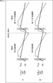
- FIG. 9 is a timing chart for explaining the operation of the column ADC for two rows corresponding to FIG. 8.
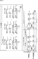
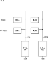
- 2 is a block diagram showing a wiring layout of pixels A and B and a column ADC for two rows in the present embodiment.
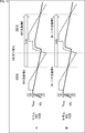
- FIG. 12 is a timing chart for explaining the operation of the column ADC for two rows corresponding to FIG. 10. It is a figure which compares the noise in the case of employ
- FIG. 18 is a block diagram illustrating a configuration example of a computer to which the present technology is applied. It is a block diagram which shows an example of a schematic structure of a vehicle control system. It is explanatory drawing which shows an example of the installation position of a vehicle exterior information detection part and an imaging part.
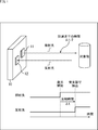
- FIG. 1 is a diagram illustrating an outline of an embodiment of a distance measuring device to which the present technology is applied.
- the distance measuring device 10 includes a light emitting unit 11 and a light receiving unit 12, and measures the distance to the object by the TOF method.
- the light emitting unit 11 emits irradiation light such as predetermined modulated light such as pulsed light applied to the object.
- the light receiving unit 12 receives the reflected light reflected from the object by the irradiated light.
- the distance measuring device 10 obtains a time (hereinafter also referred to as reflection time) ⁇ t from the emission of the irradiation light at the light emitting unit 11 to the reception of the reflected light at the light receiving unit 12, and based on the above-described equation (1).
- the distance L to the object is calculated.
- the distance L to the object can be obtained by obtaining the reflection time ⁇ t.
- the method for obtaining the reflection time ⁇ t is, for example, the first calculation method.
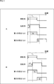
- FIG. 2 is a diagram for explaining the principle of the first calculation method of the reflection time ⁇ t.
- pulse light having a predetermined pulse width Tp is employed as the irradiation light.
- the reflected light of the irradiated light (the reflected light reflected by the target object) is received after the reflection time ⁇ t corresponding to the distance L to the target has elapsed since the irradiated light was emitted. .
- a pulse having the same pulse width and the same phase as the pulse light as the irradiation light is referred to as a first light reception pulse.
- a pulse having the same pulse width as that of the pulsed light as the irradiation light and having a phase shifted by the same width as the pulse width Tp of the pulsed light is referred to as a second received light pulse.
- reflected light is received in each of the period of the first light reception pulse (H (High) level) and the period of the second light reception pulse.
- the charge amount (received light amount) of the reflected light received during the period of the first light receiving pulse is expressed as Q1
- the charge amount of the reflected light received during the period of the second light receiving pulse is expressed as Q2.
- the reflection time ⁇ t can be obtained according to the following equation (2).
- ⁇ t Tp ⁇ Q2 / (Q1 + Q2) (2)
- the reflection time ⁇ t is proportional to the charge amount Q2. Therefore, when the distance L to the object is a short distance, the charge amount Q2 is small, and when the distance L to the object is a long distance, the charge amount Q2 is large.
- FIG. 2A shows irradiation light, reflected light, charge amount Q1 in the first light reception pulse, and charge amount Q2 in the second light reception pulse when the distance L to the object is a short distance.
- 2B shows irradiation light, reflected light, charge amount Q1 in the first light reception pulse, and charge amount Q2 in the second light reception pulse when the distance L to the object is a long distance. Represents.
- the ambient light is received in addition to the reflected light during the period of the first and second light receiving pulses, the ambient light is calculated in calculating the reflection time ⁇ t (and the distance L). It is necessary to cancel the charge amount.
- the description of the cancellation of the amount of charge of the ambient light is omitted.
- FIG. 3 is a diagram for explaining the principle of the second calculation method of the reflection time ⁇ t.
- emission of pulsed light as irradiation light is performed a plurality of times, for example, four times.
- reflected light is received by shifting the first and second light-receiving pulses by ⁇ [rad] from the case of the first calculation method.
- the phase of the pulse width Tp of the pulsed light as the irradiation light is ⁇ [rad].
- the charge amount of the reflected light received during the period of the first light reception pulse in the ⁇ -shifted light reception is expressed as TapA
- the charge amount of the reflected light received during the period of the second light reception pulse is expressed as TapB. I will do it.
- a difference TapA-TapB between the charge amounts TapA and TapB obtained by ⁇ / 2 shifted light reception, ⁇ shifted light reception, and 3 ⁇ / 2 shifted light reception is represented as difference signals Sig2, Sig3, and Sig4, respectively. I will do it.
- phase difference ⁇ between the irradiated light and the reflected light can be obtained according to the following equation (3).
- ⁇ arctan ((Sig2-Sig4) / (Sig1-Sig3)) (3)
- phase difference ⁇ and the reflection time ⁇ t have a one-to-one correspondence, and the reflection time ⁇ t can be obtained according to the following equation (4) based on the phase difference ⁇ .
- ⁇ t Tp ⁇ ⁇ / ⁇ (4)
- the present technology can be applied to both the first and second calculation methods described above, but hereinafter, the second calculation method of the first and second calculation methods will be described as an example. .
- FIG. 4 is a timing chart for explaining an example of distance measurement when the distance measuring device 10 which is a TOF sensor obtains the reflection time ⁇ t by the second calculation method.
- the distance measuring device 10 calculates the distance L in units of frames, with the period for calculating the distance L to the object as a frame.
- the frame length is, for example, 33 [ms].
- the frame includes a plurality of subframes sub that are periods in which the irradiation light is emitted.
- the length of the subframe (subframe length) is, for example, 0.2 [ms].
- the frame includes, for example, four subframes sub, and the four subframes sub are arranged from the head of the frame at a predetermined constant interval sd.
- the time of light emission and ⁇ -shifted light reception for one time (for example, the time corresponding to the phase of 2 ⁇ ) is set to 100 [ns], for example, the time of light emission and ⁇ -shifted light reception For example, 2000 times or more.
- the sum of the charge amounts of the reflected light received a plurality of times such as 2000 times is used.
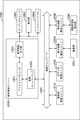
- FIG. 5 is a block diagram showing an electrical configuration example of the distance measuring device 10 shown in FIG.
- the distance measuring device 10 includes a light emitting unit 11, a light receiving unit 12, a distance calculating unit 51, and a control unit 53.
- the light emitting unit 11 is configured by, for example, an LED (Light Emitting Diode) or the like, and emits irradiation light according to the control of the control unit 53.
- LED Light Emitting Diode
- the light receiving unit 12 includes an effective pixel unit 30 and a dummy pixel unit 40. A detailed configuration example of the light receiving unit 12 will be described later with reference to FIG.
- the effective pixel unit 30 includes a plurality of pixels 31, and the dummy pixel unit 40 includes a plurality of pixels 41.
- the pixels 31 and 41 are composed of, for example, a PD (photodiode) or the like, receive light incident thereon, and generate charges corresponding to the amount of light.
- a PD photodiode
- the pixel 31 receives the reflected light of the irradiation light emitted by the light emitting unit 11 according to the control of the control unit 53, and charges corresponding to the reflected light, that is, for example, the first described in FIG.
- the charge amount TapA of the reflected light received during the period of one light reception pulse and the charge amount TapB of the reflected light received during the period of the second light reception pulse are generated and supplied to the distance calculation unit 51.
- the pixel 41 is shielded from light, for example, and functions as a so-called OPB (Optical Black) pixel.
- OPB Optical Black
- the pixel 31 that constitutes the effective pixel unit 30 and the pixel 41 that constitutes the dummy pixel unit 40 are arranged in separate areas in order to avoid complication of the drawing.
- the pixels 41 can be arranged so as to be mixed in the pixels 31, for example.
- the distance calculation unit 51 calculates the phase difference ⁇ using the charge amount of the charge from the pixel 31, for example, as described in FIG. 3, and based on the reflection time ⁇ t obtained from the phase difference ⁇ , the target Calculate the distance L to the object.
- the distance calculation unit 51 calculates a distance L for each pixel 31 constituting the effective pixel unit 30, and outputs a distance image having the pixel value as the distance L (a value corresponding to the distance L) as distance information. .
- the control unit 53 controls the emission of irradiation light by the light emitting unit 11 and the reception of reflected light by the pixels 31 of the light receiving unit 12.
- FIG. 6 is a block diagram illustrating a configuration example of the light receiving unit 12.
- the light receiving section 12 is configured in substantially the same manner as a solid-state imaging device such as a CMOS image sensor employing a column parallel ADC (Analog Digital Converter).
- a solid-state imaging device such as a CMOS image sensor employing a column parallel ADC (Analog Digital Converter).
- the light receiving unit 12 includes a pixel unit 101, a column ADC 102, a horizontal transfer scanning circuit 103, a digital-analog converter (DAC) 104, and a vertical scanning circuit 105.
- DAC digital-analog converter
- the pixel unit 101 corresponds to the effective pixel unit 30 and the dummy pixel unit 40 of FIG. 5, and is configured by unit pixels 121 including PDs and cock-type pixels Tr. (Transistors) arranged in a matrix (matrix).
- the unit pixel 121 corresponds to the pixels 31 and 41 in FIG.
- pixel drive lines (not shown) are formed for each row in a matrix-like pixel arrangement along the horizontal direction in the figure (pixel arrangement direction of the pixel row), and vertical signal lines are provided for each column.
- 122-1 to 122-N are formed along the vertical direction in the drawing (pixel arrangement direction of the pixel column).
- the vertical signal lines 122-1 to 122 -N are simply referred to as the vertical signal lines 122 when it is not necessary to distinguish them individually. The same description is applied to other parts.
- the vertical scanning circuit 105 is a pixel driving unit that drives the pixels 121 of the pixel unit 101 at the same time or in units of rows according to control from the control unit 53.
- the vertical scanning circuit 105 is configured to have a readout scanning system and a sweep scanning system, or batch sweep and batch transfer, although illustration of the specific configuration is omitted.
- Pixel signals output from each unit pixel 121 of the pixel row selectively scanned by the vertical scanning circuit 105 are supplied to the column ADCs 102-1 to 102-N via the vertical signal lines 122-1 to 122-N, respectively.
- the column ADC 102 includes a comparator 141 and a counter 142. For each pixel column of the pixel unit 101, the column ADC 102 has a predetermined voltage signal VSL as a pixel signal output from each unit pixel 121 in the selected row through the vertical signal line 122. Is supplied to the horizontal transfer scanning circuit 103.
- FIG. 7 is a timing chart for explaining the signal processing of the column ADC 102.
- the counter 141 starts the count operation of the counter 142 at the same time as the sweep of the reference voltage Vramp supplied from the DAC 104 is started by the comparator 141. Then, at the timing when the reference voltage Vramp falls below the voltage signal VSL, the output signal VCO of the comparator 141 is inverted from the high level to the low level. At the falling edge, the counting operation of the counter 142 is stopped.
- the count value VCNT has a one-to-one relationship with the voltage width swept by the reference voltage Vramp, and this count value VCNT is supplied to the subsequent horizontal transfer scanning circuit 103 as a result of AD conversion of the input voltage.
- the horizontal transfer scanning circuit 103 sequentially selects unit circuits corresponding to the pixel columns of the column ADCs 102-1 to 102-N. By the selective scanning by the horizontal transfer scanning circuit 103, the pixel signals processed by the column ADC 102 are sequentially output to the distance calculation unit 51.
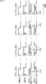
- FIG. 8 illustrates two rows of pixels A and B, two columns of vertical signal lines 122A and 122B, and two columns of columns ADCs 102A and 102B in the pixel unit 101 of FIG. It is a block diagram which shows an example of a wiring layout.
- the pixel A in the Nth row and the pixel A in the N + 1st row are connected to the column ADC 102A through the vertical signal line 122A.
- the pixel B in the Nth row and the pixel B in the N + 1st row are connected to the column ADC 102B via the vertical signal line 122B.
- the pixel A that outputs the charge amount TapA of the difference TapA-TapB and the pixel B that outputs the charge amount TapB are connected to different column ADCs 102, respectively.
- the column ADC 102A and the column ADC 102B may perform one operation (first operation) simultaneously.
- the column ADC 102A and the column ADC 102B may perform one operation (second operation) simultaneously.
- FIG. 9 is a timing chart showing the operation of the column ADCs 102A and 102B in the wiring layout shown in FIG.
- FIG. 7A shows the operation of the column ADC 102A
- FIG. 7B shows the operation of the column ADC 102B.
- the column ADCs 102A and 102B perform auto-zero processing for offsetting the voltage signal VSL at the beginning of each operation.
- the column ADC 102A and the column ADC 102B When calculating the difference TapA-TapB from the output of the pixels A and B for one row (for example, the Nth row), the column ADC 102A and the column ADC 102B simultaneously perform one operation (first operation). Just do it. Therefore, if the column ADC 102A and the column ADC 102B simultaneously perform two operations (the first operation and the second operation), the pixels A and B in two rows (for example, the Nth row and the N + 1th row) The difference TapA-TapB can be calculated from the output.
- the column ADC 102 is not subjected to the CDS process having the noise removal effect because the high speed is required for the operation. Therefore, mainly low frequency noise represented by 1 / f noise applied by the comparator 141 remains mixed in the output of the column ADC 102. If low-frequency noise is mixed in the output of the column ADC 102, an error also occurs in the difference TapA-TapB calculated by the distance calculation unit 51 in the subsequent stage, and as a result, the object to be finally calculated is calculated. The error of the distance L also becomes large.
- the wiring shown in FIG. 8 is obtained so that the low frequency noise can be removed in the same way as the CDS process when the difference TapA ⁇ TapB is calculated by the distance calculation unit 51.
- the layout has been changed.
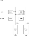
- ⁇ Wiring Layout of Pixels A and B and Column ACD102 in this Embodiment> 10 shows two rows of pixels A and B, two columns of vertical signal lines 122A and 122B, and two columns of columns ADCs 102A and 102B in the pixel portion 101 of FIG. It is a block diagram which shows the wiring layout in this Embodiment.
- the pixel A and the pixel B in the Nth row are connected to the column ADC 102A via the vertical signal line 122A.
- the pixel A and the pixel B in the (N + 1) th row are connected to the column ADC 102B via the vertical signal line 122B.
- the pixel A that outputs the charge amount TapA of the difference TapA-TapB and the pixel B that outputs the charge amount TapB are connected to the same column ADC102.
- the column ADC 102A When calculating the difference TapA-TapB from the outputs of the pixels A and B in the Nth row, the column ADC 102A performs AD conversion on the output of the pixel A in the Nth row as the first operation, and then the second operation.
- the output of the pixel B in the Nth row may be AD converted.
- the column ADC 102B can perform the second operation simultaneously with the column ADC 102A performing the first and second operations. Specifically, the column ADC 102B AD-converts the output of the pixel A in the (N + 1) th row as the first operation, and then AD-converts the output of the pixel B in the (N + 1) th row as the second operation. it can.
- FIG. 11 is a timing chart showing the operation of the column ADCs 102A and 102B in the wiring layout shown in FIG.
- FIG. 7A shows the operation of the column ADC 102A
- FIG. 7B shows the operation of the column ADC 102B.
- the column ADCs 102A and 102B perform auto-zero processing only at the beginning of the first operation, and omit auto-zero processing in the second operation.
- the outputs of the pixels A and B in the Nth row are AD converted by the same column ADC 102A.
- the outputs of the pixels A and B in the (N + 1) th row are AD converted by the same column ADC 102B. Therefore, when the difference TapA-TapB is calculated by the distance calculation unit 51 in the subsequent stage, the calculation result includes a high-pass filter effect (low-frequency noise removal effect) by a high-pass filter function (the following equation (5)) by difference extraction.
- High-pass filter function H ( ⁇ ) ⁇ (2-2COS (2 ⁇ Fnoise Tcds)) ... (5)
- the outputs of the pixels A and B in the Nth row are AD-converted by the same column ADC 102A, the outputs of the pixels A and B in the Nth row are different as in the case of the wiring layout shown in FIG. Compared with the case where AD conversion is performed by the column ADCs 102 ⁇ / b> A and 102 ⁇ / b> B, variation in AD conversion characteristics between columns can be suppressed.
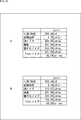
- FIG. 12 shows noise mixed in the difference TapA-TapB in the distance calculation unit 51 in the subsequent stage when the wiring layout of FIG. 8 and the wiring layout of FIG. 10 are adopted.
- FIG. 9A corresponds to the wiring layout of FIG. 8
- FIG. B corresponds to the wiring layout of FIG.
- CM noise common mode
- total noise can be reduced by about 10%.
- the series of processes described above can be executed by hardware or can be executed by software.
- a program constituting the software is installed in the computer.
- the computer includes, for example, a general-purpose personal computer capable of executing various functions by installing a computer incorporated in dedicated hardware and various programs.
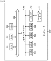
- FIG. 13 is a block diagram showing an example of the hardware configuration of a computer that executes the above-described series of processing by a program.
- a CPU Central Processing Unit
- ROM Read Only Memory
- RAM Random Access Memory
- An input / output interface 205 is further connected to the bus 204.
- An input unit 206, an output unit 207, a storage unit 208, a communication unit 209, and a drive 210 are connected to the input / output interface 205.
- the input unit 206 includes a keyboard, a mouse, a microphone, and the like.
- the output unit 207 includes a display, a speaker, and the like.
- the storage unit 208 includes a hard disk, a nonvolatile memory, and the like.
- the communication unit 209 includes a network interface and the like.
- the drive 210 drives a removable medium 211 such as a magnetic disk, an optical disk, a magneto-optical disk, or a semiconductor memory.
- the CPU 201 loads the program stored in the storage unit 208 to the RAM 203 via the input / output interface 205 and the bus 204 and executes the program. A series of processing is performed.
- the program executed by the computer (CPU 201) can be provided by being recorded in the removable medium 211 as a package medium or the like, for example.
- the program can be provided via a wired or wireless transmission medium such as a local area network, the Internet, or digital satellite broadcasting.
- the program can be installed in the storage unit 208 via the input / output interface 205 by attaching the removable medium 211 to the drive 210.
- the program can be received by the communication unit 209 via a wired or wireless transmission medium and installed in the storage unit 208.
- the program can be installed in the ROM 202 or the storage unit 208 in advance.
- the program executed by the computer 200 may be a program that is processed in time series in the order described in this specification, or a necessary timing such as when a call is made in parallel. It may be a program in which processing is performed.
- the technology according to the present disclosure can be applied to various products.
- the technology according to the present disclosure is realized as a device that is mounted on any type of mobile body such as an automobile, an electric vehicle, a hybrid electric vehicle, a motorcycle, a bicycle, personal mobility, an airplane, a drone, a ship, and a robot. May be.
- FIG. 14 is a block diagram illustrating a schematic configuration example of a vehicle control system that is an example of a mobile control system to which the technology according to the present disclosure can be applied.
- the vehicle control system 12000 includes a plurality of electronic control units connected via a communication network 12001.
- the vehicle control system 12000 includes a drive system control unit 12010, a body system control unit 12020, a vehicle exterior information detection unit 12030, a vehicle interior information detection unit 12040, and an integrated control unit 12050.
- a microcomputer 12051, an audio image output unit 12052, and an in-vehicle network I / F (interface) 12053 are illustrated.
- the drive system control unit 12010 controls the operation of the device related to the drive system of the vehicle according to various programs.
- the drive system control unit 12010 includes a driving force generator for generating a driving force of a vehicle such as an internal combustion engine or a driving motor, a driving force transmission mechanism for transmitting the driving force to wheels, and a steering angle of the vehicle. It functions as a control device such as a steering mechanism that adjusts and a braking device that generates a braking force of the vehicle.
- the body system control unit 12020 controls the operation of various devices mounted on the vehicle body according to various programs.
- the body system control unit 12020 functions as a keyless entry system, a smart key system, a power window device, or a control device for various lamps such as a headlamp, a back lamp, a brake lamp, a blinker, or a fog lamp.
- the body control unit 12020 can be input with radio waves transmitted from a portable device that substitutes for a key or signals from various switches.
- the body system control unit 12020 receives input of these radio waves or signals, and controls a door lock device, a power window device, a lamp, and the like of the vehicle.
- the vehicle outside information detection unit 12030 detects information outside the vehicle on which the vehicle control system 12000 is mounted.
- the imaging unit 12031 is connected to the vehicle exterior information detection unit 12030.
- the vehicle exterior information detection unit 12030 causes the imaging unit 12031 to capture an image outside the vehicle and receives the captured image.
- the vehicle outside information detection unit 12030 may perform an object detection process or a distance detection process such as a person, a car, an obstacle, a sign, or a character on a road surface based on the received image.
- the imaging unit 12031 is an optical sensor that receives light and outputs an electrical signal corresponding to the amount of received light.
- the imaging unit 12031 can output an electrical signal as an image, or can output it as distance measurement information. Further, the light received by the imaging unit 12031 may be visible light or invisible light such as infrared rays.
- the vehicle interior information detection unit 12040 detects vehicle interior information.
- a driver state detection unit 12041 that detects a driver's state is connected to the in-vehicle information detection unit 12040.
- the driver state detection unit 12041 includes, for example, a camera that images the driver, and the vehicle interior information detection unit 12040 determines the degree of fatigue or concentration of the driver based on the detection information input from the driver state detection unit 12041. It may be calculated or it may be determined whether the driver is asleep.
- the microcomputer 12051 calculates a control target value of the driving force generator, the steering mechanism, or the braking device based on the information inside / outside the vehicle acquired by the vehicle outside information detection unit 12030 or the vehicle interior information detection unit 12040, and the drive system control unit A control command can be output to 12010.
- the microcomputer 12051 realizes an ADAS (Advanced Driver Assistance System) function including vehicle collision avoidance or impact mitigation, following traveling based on inter-vehicle distance, vehicle speed maintaining traveling, vehicle collision warning, or vehicle lane departure warning, etc. It is possible to perform cooperative control for the purpose.
- ADAS Advanced Driver Assistance System
- the microcomputer 12051 controls the driving force generator, the steering mechanism, the braking device, and the like based on the information around the vehicle acquired by the vehicle exterior information detection unit 12030 or the vehicle interior information detection unit 12040. It is possible to perform cooperative control for the purpose of automatic driving that autonomously travels without depending on the operation.
- the microcomputer 12051 can output a control command to the body system control unit 12020 based on information outside the vehicle acquired by the vehicle outside information detection unit 12030.
- the microcomputer 12051 controls the headlamp according to the position of the preceding vehicle or the oncoming vehicle detected by the outside information detection unit 12030, and performs cooperative control for the purpose of anti-glare, such as switching from a high beam to a low beam. It can be carried out.
- the sound image output unit 12052 transmits an output signal of at least one of sound and image to an output device capable of visually or audibly notifying information to a vehicle occupant or the outside of the vehicle.
- an audio speaker 12061, a display unit 12062, and an instrument panel 12063 are illustrated as output devices.
- the display unit 12062 may include at least one of an on-board display and a head-up display, for example.
- FIG. 15 is a diagram illustrating an example of an installation position of the imaging unit 12031.
- the vehicle 12100 includes imaging units 12101, 12102, 12103, 12104, and 12105 as the imaging unit 12031.
- the imaging units 12101, 12102, 12103, 12104, and 12105 are provided, for example, at positions such as a front nose, a side mirror, a rear bumper, a back door, and an upper part of a windshield in the vehicle interior of the vehicle 12100.
- the imaging unit 12101 provided in the front nose and the imaging unit 12105 provided in the upper part of the windshield in the vehicle interior mainly acquire an image in front of the vehicle 12100.
- the imaging units 12102 and 12103 provided in the side mirror mainly acquire an image of the side of the vehicle 12100.
- the imaging unit 12104 provided in the rear bumper or the back door mainly acquires an image behind the vehicle 12100.
- the forward images acquired by the imaging units 12101 and 12105 are mainly used for detecting a preceding vehicle or a pedestrian, an obstacle, a traffic light, a traffic sign, a lane, or the like.
- FIG. 15 shows an example of the shooting range of the imaging units 12101 to 12104.
- the imaging range 12111 indicates the imaging range of the imaging unit 12101 provided in the front nose
- the imaging ranges 12112 and 12113 indicate the imaging ranges of the imaging units 12102 and 12103 provided in the side mirrors, respectively
- the imaging range 12114 The imaging range of the imaging part 12104 provided in the rear bumper or the back door is shown. For example, by superimposing the image data captured by the imaging units 12101 to 12104, an overhead image when the vehicle 12100 is viewed from above is obtained.
- At least one of the imaging units 12101 to 12104 may have a function of acquiring distance information.
- at least one of the imaging units 12101 to 12104 may be a stereo camera including a plurality of imaging elements, or may be an imaging element having pixels for phase difference detection.
- the microcomputer 12051 based on the distance information obtained from the imaging units 12101 to 12104, the distance to each three-dimensional object in the imaging range 12111 to 12114 and the temporal change in this distance (relative speed with respect to the vehicle 12100).
- a predetermined speed for example, 0 km / h or more
- the microcomputer 12051 can set an inter-vehicle distance to be secured in advance before the preceding vehicle, and can perform automatic brake control (including follow-up stop control), automatic acceleration control (including follow-up start control), and the like.
- automatic brake control including follow-up stop control
- automatic acceleration control including follow-up start control
- cooperative control for the purpose of autonomous driving or the like autonomously traveling without depending on the operation of the driver can be performed.
- the microcomputer 12051 converts the three-dimensional object data related to the three-dimensional object to other three-dimensional objects such as a two-wheeled vehicle, a normal vehicle, a large vehicle, a pedestrian, and a utility pole based on the distance information obtained from the imaging units 12101 to 12104. It can be classified and extracted and used for automatic avoidance of obstacles.
- the microcomputer 12051 identifies obstacles around the vehicle 12100 as obstacles that are visible to the driver of the vehicle 12100 and obstacles that are difficult to see.
- the microcomputer 12051 determines the collision risk indicating the risk of collision with each obstacle, and when the collision risk is equal to or higher than the set value and there is a possibility of collision, the microcomputer 12051 is connected via the audio speaker 12061 or the display unit 12062. By outputting an alarm to the driver and performing forced deceleration or avoidance steering via the drive system control unit 12010, driving assistance for collision avoidance can be performed.
- At least one of the imaging units 12101 to 12104 may be an infrared camera that detects infrared rays.
- the microcomputer 12051 can recognize a pedestrian by determining whether a pedestrian is present in the captured images of the imaging units 12101 to 12104. Such pedestrian recognition is, for example, whether or not the user is a pedestrian by performing a pattern matching process on a sequence of feature points indicating the outline of an object and a procedure for extracting feature points in the captured images of the imaging units 12101 to 12104 as infrared cameras. It is carried out by the procedure for determining.
- the audio image output unit 12052 When the microcomputer 12051 determines that there is a pedestrian in the captured images of the imaging units 12101 to 12104 and recognizes the pedestrian, the audio image output unit 12052 has a rectangular contour line for emphasizing the recognized pedestrian.
- the display unit 12062 is controlled so as to be superimposed and displayed.
- voice image output part 12052 may control the display part 12062 so that the icon etc. which show a pedestrian may be displayed on a desired position.
- the present technology can also have the following configurations.
- a light emitting unit for emitting irradiation light;
- a light receiving unit that includes a plurality of pixels, and receives the reflected light reflected from the object by the irradiation light;
- a calculation unit that calculates a distance to the object based on a time from emission of the irradiation light to reception of the reflected light;
- a control unit for controlling the emission of the irradiation light
- the light receiving unit includes a plurality of AD conversion units that AD convert pixel signals read from the pixels, The first and second pixel signals read from each of the adjacent first pixel and second pixel among the plurality of pixels forming the light receiving unit are AD-converted by the same AD conversion unit,
- the calculation unit is configured to calculate the time from the emission of the irradiation light to the reception of the reflected light, and the first pixel signal and the second pixel that are AD-converted by the same AD conversion unit Ranging device that calculates the difference from the signal
- the first and second pixel signals read from each of the adjacent first and second pixels in the same row or the same column are the same AD conversion.
- the AD conversion unit performs AD conversion on the first pixel signal read from the first pixel, and then AD converts the second pixel signal read from the second pixel.
- the AD conversion unit performs auto-zero processing when AD converting the first pixel signal read from the first pixel, and AD converts the second pixel signal read from the second pixel
- the distance measuring device according to any one of (1) to (3), wherein auto-zero processing is omitted.
- the light emitting unit emits irradiation light to the outside of the vehicle.
- a light receiving unit that includes a plurality of pixels, and receives the reflected light reflected from the object by the irradiation light;
- a calculation unit that calculates a distance to the object based on a time from emission of the irradiation light to reception of the reflected light;
- the light receiving unit includes a plurality of AD conversion units that AD convert pixel signals read from the pixels.
- the AD conversion of the first and second pixel signals read from each of the adjacent first pixel and second pixel among the plurality of pixels forming the light receiving unit by the same AD conversion unit In the process of calculating the time from the emission of the irradiation light to the reception of the reflected light, the difference between the first pixel signal and the second pixel signal that are AD-converted by the same AD conversion unit is calculated.
- Ranging method that includes a step to calculate.
Landscapes
- Engineering & Computer Science (AREA)
- Physics & Mathematics (AREA)
- General Physics & Mathematics (AREA)
- Radar, Positioning & Navigation (AREA)
- Remote Sensing (AREA)
- Computer Networks & Wireless Communication (AREA)
- Electromagnetism (AREA)
- Multimedia (AREA)
- Signal Processing (AREA)
- Optical Radar Systems And Details Thereof (AREA)
- Measurement Of Optical Distance (AREA)
- Transforming Light Signals Into Electric Signals (AREA)
Abstract
本技術は、対象物からの反射光に基づく画素信号にノイズが生じることを抑止して、測距の精度を維持することができるようにする測距装置、および測距方法に関する。 本技術の一側面である測距装置は、照射光を発光する発光部と、前記照射光が対象物において反射した反射光を受光する受光部と、前記照射光の発光から前記反射光の受光までの時間に基づいて、前記対象物までの距離を算出する算出部と、前記照射光の発光を制御する制御部とを備え、前記受光部は、前記画素から読み出される画素信号をAD変換する複数のAD変換部を有し、前記受光部を成す複数の画素のうち、隣接する第1の画素と第2の画素のそれぞれから読み出される第1および第2の画素信号は、同一の前記AD変換部によってAD変換され、前記算出部は、前記時間を算出する過程において、前記同一の前記AD変換部によってAD変換されている前記第1の画素信号と前記第2の画素信号との差分を演算する。
Description
本技術は、測距装置、および測距方法に関し、特に、低周波ノイズに起因する測距精度の低下を抑止できるようにした測距装置、および測距方法に関する。
対象物までの距離を測定する(以下、測距を行うとも称する)測距装置としてTOF(Time Of Flight)センサが知れている(例えば、特許文献1参照)。
TOFセンサは、対象物に照射する光である照射光を発光し、その照射光が対象物において反射した反射光を受光することで、照射光の発光から反射光の受光までの時間、すなわち、照射光が対象物で反射されて戻ってくるまでの反射時間Δtを求めている。そして、この反射時間Δtと光速c[m/s]とを用い、次式(1)に基づいて対象物までの距離Lを演算している。
L=c×Δt/2 ・・・(1)
L=c×Δt/2 ・・・(1)
上述したように、TOFセンサでは、照射光が対象物で反射されて戻ってくるまでの時間Δtを求めており、反射光を受光するための構成として、例えばCMOSイメージセンサ等と同様に構成される固体撮像素子が採用されている。したがって、該固体撮像素子が出力する画素信号にノイズが生じてしまうと、照射光が対象物で反射されて戻ってくるまでの時間Δtを正確に求めることができなくなり、対象物の測距の精度が低下してしまうことになる。
本技術は、このような状況に鑑みてなされたものであり、対象物からの反射光に基づく画素信号にノイズが生じることを抑止して、測距の精度を維持できるようにするものである。
本技術の一側面である測距装置は、照射光を発光する発光部と、複数の画素から成り、前記照射光が対象物において反射した反射光を受光する受光部と、前記照射光の発光から前記反射光の受光までの時間に基づいて、前記対象物までの距離を算出する算出部と、前記照射光の発光を制御する制御部とを備え、前記受光部は、前記画素から読み出される画素信号をAD変換する複数のAD変換部を有し、前記受光部を成す複数の画素のうち、隣接する第1の画素と第2の画素のそれぞれから読み出される第1および第2の画素信号は、同一の前記AD変換部によってAD変換され、前記算出部は、前記照射光の発光から前記反射光の受光までの時間を算出する過程において、前記同一の前記AD変換部によってAD変換されている前記第1の画素信号と前記第2の画素信号との差分を演算する。
前記受光部を成す複数の画素のうち、同一の行または同一の列において隣接する第1の画素と第2の画素のそれぞれから読み出される第1および第2の画素信号は、同一の前記AD変換部によってAD変換されるようにすることができる。
前記AD変換部は、前記第1の画素から読み出される前記第1の画素信号をAD変換した後、前記第2の画素から読み出される前記第2の画素信号をAD変換することができる。
前記AD変換部は、前記第1の画素から読み出される前記第1の画素信号をAD変換する際にオートゼロ処理を実行し、前記第2の画素から読み出される前記第2の画素信号をAD変換する際にオートゼロ処理を省略することができる。
本技術の一側面である測距装置は、車両に搭載することができ、前記発光部は、前記車両の外部に照射光を発光することができる。
本技術の一側面である測距方法は、照射光を発光する発光部と、複数の画素から成り、前記照射光が対象物において反射した反射光を受光する受光部と、前記照射光の発光から前記反射光の受光までの時間に基づいて、前記対象物までの距離を算出する算出部と、前記照射光の発光を制御する制御部とを備え、前記受光部は、前記画素から読み出される画素信号をAD変換する複数のAD変換部を有する測距装置の測距方法において、前記受光部を成す複数の画素のうち、隣接する第1の画素と第2の画素のそれぞれから読み出される第1および第2の画素信号を同一の前記AD変換部によってAD変換し、前記照射光の発光から前記反射光の受光までの時間を算出する過程において、前記同一の前記AD変換部によってAD変換されている前記第1の画素信号と前記第2の画素信号との差分を演算するステップを含む。
本技術の一側面においては、受光部を成す複数の画素のうち、隣接する第1の画素と第2の画素のそれぞれから読み出される第1および第2の画素信号が同一のAD変換部によってAD変換され、照射光の発光から反射光の受光までの時間を算出する過程において、同一のAD変換部によってAD変換されている第1の画素信号と第2の画素信号との差分が演算される。
本技術の一側面によれば、対象物からの反射光に基づく画素信号にノイズが生じることを抑止できる。よって、測距の精度を維持することが可能となる。
以下、本技術を実施するための最良の形態(以下、実施の形態と称する)について、図面を参照しながら詳細に説明する。
<本技術を適用した測距装置の一実施の形態>
図1は、本技術を適用した測距装置の一実施の形態の概要を説明する図である。
測距装置10は、発光部11および受光部12を有し、TOF方式で、対象物までの距離を測定する。
発光部11は、対象物に照射するパルス光等の所定の変調光等である照射光を発光する。
受光部12は、照射光が対象物において反射した反射光を受光する。
測距装置10は、発光部11での照射光の発光から、受光部12での反射光の受光までの時間(以下、反射時間ともいう)Δtを求め、上述した式(1)に基づいて対象物までの距離Lを算出する。
したがって、対象物までの距離Lは、反射時間Δtを求めることにより得ることができるが、測距装置10を含むTOFセンサにおいて、反射時間Δtを求める方法としては、例えば、第1の算出方法と第2の算出方法とがある。
<反射時間Δtの第1の算出方法>
図2は、反射時間Δtの第1の算出方法の原理を説明する図である。
ここで、照射光として、例えば所定のパルス幅Tpのパルス光を採用することとする。
TOFセンサでは、照射光が発光されてから、対象物までの距離Lに応じた反射時間Δtだけ経過した後に、照射光の反射光(照射光が対象物で反射した反射光)が受光される。
いま、照射光としてのパルス光と同一のパルス幅であって、位相が等しいパルスを第1の受光パルスと称することにする。また、照射光としてのパルス光と同一のパルス幅であって、位相がパルス光のパルス幅Tpと同じ幅だけずれたパルスを第2の受光パルスと称することにする。
第1の算出方法では、第1の受光パルスの(H(High)レベルの)期間と、第2の受光パルスの期間とのそれぞれの期間において、反射光が受光される。
いま、第1の受光パルスの期間に受光された反射光の電荷量(受光量)をQ1と表すとともに、第2の受光パルスの期間に受光された反射光の電荷量をQ2と表すことにする。
この場合、反射時間Δtは次式(2)に従って求めることができる。
△t=Tp×Q2/(Q1+Q2) ・・・(2)
△t=Tp×Q2/(Q1+Q2) ・・・(2)
式(2)から分かるように、反射時間Δtは、電荷量Q2に比例する。よって、対象物までの距離Lが近距離である場合、電荷量Q2は小さくなり、対象物までの距離Lが遠距離である場合、電荷量Q2は大きくなる。
図2のAは、対象物までの距離Lが近距離である場合の照射光、反射光、第1の受光パルスのおける電荷量Q1、および第2の受光パルスのおける電荷量Q2を表しており、図2のBは、対象物までの距離Lが遠距離である場合の照射光、反射光、第1の受光パルスのおける電荷量Q1、および第2の受光パルスのおける電荷量Q2を表している。
なお、実際には、第1および第2の受光パルスの期間においては、反射光の他、環境光も受光されるため、反射時間Δt(延いては距離L)の算出にあたっては、環境光の電荷量をキャンセルする必要がある。但し、本実施の形態では、説明を簡単にするため、環境光の電荷量のキャンセルについては説明を省略する。
<反射時間Δtの第2の算出方法>
図3は、反射時間Δtの第2の算出方法の原理を説明する図である。
第2の算出方法では、照射光としてのパルス光の発光が、複数回、例えば4回行われる。
そして、4回のパルス光の発光に対して、0ずらし受光、π/2ずらし受光、πずらし受光、および、3π/2ずらし受光が、それぞれ行われる。
θずらし受光では、第1および第2の受光パルスを、第1の算出方法の場合から、θ[rad]だけずらして、反射光の受光が行われる。ここで、照射光としてのパルス光のパルス幅Tpの位相がπ[rad]である。
いま、θずらし受光における第1の受光パルスの期間に受光された反射光の電荷量を、TapAと表すとともに、第2の受光パルスの期間に受光された反射光の電荷量を、TapBと表すこととする。
そして、0ずらし受光で得られた電荷量TapAとTapBとの差分TapA-TapBを差信号Sig1と表すこととする。
同様に、π/2ずらし受光、πずらし受光、および、3π/2ずらし受光で得られた電荷量TapAとTapBとの差分TapA-TapBを、差信号Sig2,Sig3、および、Sig4と、それぞれ表すこととする。
この場合、照射光と反射光との位相差φは、次式(3)に従って求めることができる。
φ=arctan((Sig2-Sig4)/(Sig1-Sig3)) ・・・(3)
φ=arctan((Sig2-Sig4)/(Sig1-Sig3)) ・・・(3)
さらに、位相差φと反射時間Δtとは一対一に対応し、反射時間Δtは、位相差φに基づき、次式(4)に従って求めることができる。
Δt=Tp×φ/π ・・・(4)
Δt=Tp×φ/π ・・・(4)
本技術は、上述した第1および第2の算出方法のいずれにも適用することができるが、以下では、第1および第2の算出方法のうち、第2の算出方法を例に説明を行う。
<測距の例>
図4は、TOFセンサである測距装置10が、第2の算出方法により反射時間Δtを求める場合の測距の例を説明するタイミングチャートである。
測距装置10では、対象物までの距離Lを算出する期間をフレームとして、フレーム単位で、距離Lを算出する。図4では、フレームの長さ(フレーム長)は、例えば、33[ms]になっている。
フレームは、照射光を発光する期間である複数のサブフレームsubを含む。
図4では、サブフレームの長さ(サブフレーム長)は、例えば、0.2[ms]になっている。
さらに、図4では、フレームは、例えば、4個のサブフレームsubを含み、その4個のサブフレームsubは、所定の一定の間隔sdで、フレームの先頭から配置されている。4個のサブフレームsubの先頭から終わりまでの長さは、例えば、1[ms]になっており、したがって、図4のフレームでは、先頭から1[ms]の期間に、4個のサブフレームsubが存在し、残りの32(=33-1)[ms]の期間は、サブフレームが存在しない期間になっている。
フレームにおいて、4個のサブフレームsubでは、0ずらし受光、π/2ずらし受光、πずらし受光、および、3π/2ずらし受光が、それぞれ行われる。
サブフレームsubでは、1回の照射光の発光およびθずらし受光の時間(例えば、2πの位相に対応する時間)を、例えば、100[ns]として、照射光の発光およびθずらし受光の時間が、例えば、2000回等の複数回繰り返される。
図3で説明した照射光と反射光との位相差φの算出には、2000回等の複数回受光された反射光の電荷量の総和が用いられる。
<測距装置10の構成例>
図5は、図1に示された測距装置10の電気的な構成例を示すブロック図である。
該測距装置10は、発光部11、受光部12、距離算出部51、および、制御部53を有する。
発光部11は、例えば、LED(Light Emitting Diode)等で構成され、制御部53の制御に従って、照射光を発光する。
受光部12は、有効画素部30およびダミー画素部40を有する。なお、受光部12の詳細な構成例については、図6を参照して後述する。
有効画素部30は、複数の画素31を有し、ダミー画素部40は、複数の画素41を有する。
画素31および41は、例えば、PD(フォトダイオード)等で構成され、そこに入射する光を受光し、その光の光量に対応する電荷を発生する。
有効画素部30では、画素31が、制御部53の制御に従って、発光部11が発光した照射光の反射光を受光し、その反射光に応じた電荷、すなわち、例えば、図3で説明した第1の受光パルスの期間に受光された反射光の電荷量TapA、および、第2の受光パルスの期間に受光された反射光の電荷量TapBを生成して距離算出部51に供給する。
ダミー画素部40では、画素41は、例えば、遮光されており、いわゆるOPB(Optical Black)画素として機能する。
なお、図5に示された構成例では、図が煩雑になるのを避けるため、有効画素部30を構成する画素31と、ダミー画素部40を構成する画素41とを、別個のエリアに配置してあるが、画素41は、例えば、画素31の中に混在するように配置することができる。
距離算出部51は、画素31からの電荷の電荷量を用いて、例えば、図3で説明したように、位相差φを算出し、その位相差φから求められる反射時間Δtに基づいて、対象物までの距離Lを算出する。距離算出部51は、有効画素部30を構成する各画素31に対して、距離Lを算出し、その距離L(に対応する値)を画素値とする距離画像等を、距離情報として出力する。
制御部53は、発光部11による照射光の発光、および、受光部12の画素31による反射光の受光を制御する。
<受光部12の構成例>
図6は、受光部12の構成例を示すブロック図である。
図6は、受光部12の構成例を示すブロック図である。
同図に示されるように、該受光部12は、列並列ADC(Analog Digital Converter)が採用されたCMOSイメージセンサ等の固体撮像素子と略同様に構成される。
受光部12は、画素部101、カラムADC102、水平転送走査回路103、デジタル-アナログ変換装置(DAC)104、および垂直走査回路105から構成されている。
画素部101は、図5の有効画素部30およびダミー画素部40に相当し、PDとカック種の画素Tr.(トランジスタ)を含む単位画素121がマトリクス状(行列状)に配置されて構成される。該単位画素121は、図5の画素31,41に相当する。
また画素部101は、行列状の画素配列に対して行毎に画素駆動線(不図示)が図の左右方向(画素行の画素の配列方向)に沿って形成され、列ごとに垂直信号線122-1乃至122-Nが図の上下方向(画素列の画素の配列方向)に沿って形成されている。なお、以下の説明において、垂直信号線122-1乃至122-Nを個々に区別する必要がない場合、単に垂直信号線122と記述する。他の部分も同様の記載を行う。
垂直走査回路105は、制御部53からの制御に従い、画素部101の画素121を、全画素同時または行単位等で駆動する画素駆動部である。この垂直走査回路105は、その具体的な構成については図示を省略するが、読み出し走査系と、掃き出し走査系あるいは、一括掃き出し、一括転送を有する構成となっている。
垂直走査回路105によって選択走査された画素行の各単位画素121から出力される画素信号は、垂直信号線122-1乃至122-Nの各々を介してカラムADC102-1乃至102-Nに供給される。カラムADC102は、比較器141とカウンタ142から構成され、画素部101の画素列ごとに、選択行の各単位画素121から垂直信号線122を通して出力される画素信号としての電圧信号VSLに対して所定の信号処理を行い、水平転送走査回路103に供給される。
ここで、カラムADC102における信号処理について説明する。カラムADC102では動作に高速性が要求されるため、いわゆる、D相レベルのみを検出しており、P相レベルを検出していない。したがって、一般的なCMOSイメージセンサにおけるカラムADCにて行われているD相レベルとP相レベルの差分を出力するCDS(相関2重サンプリング)処理は行われていない。なお、CDS処理はノイズ除去効果を有する。
図7は、カラムADC102の信号処理を説明するタイミングチャートである。
カラムADC102においては、比較器141でDAC104から供給される参照電圧Vrampのスイープが開始されると同時に、カウンタ142のカウント動作が開始される。そして、参照電圧Vrampが電圧信号VSLを下回ったタイミングに、比較器141の出力信号VCOがハイレベルからローレベルに反転する。この立ち下りエッジでカウンタ142のカウント動作が停止される。カウント値VCNTは参照電圧Vrampがスイープした電圧幅と1対1の関係であり、このカウント値VCNTが、入力電圧をAD変換した結果として、後段の水平転送走査回路103に供給される。
図6に戻る。水平転送走査回路103は、カラムADC102-1乃至102-Nの画素列に対応する単位回路を順番に選択する。この水平転送走査回路103による選択走査により、カラムADC102で信号処理された画素信号が順番に距離算出部51に出力される。
<カラムADC102におけるノイズについて>
上述したように、カラムADC102の後段に位置する距離算出部51では、θ(=0,π/2,π,3π/2)ずらし受光で得られた電荷量TapAとTapBとの差分TapA-TapBを算出している。なお、電荷量TapAを生成する画素と電荷量TapBを生成する画素は、通常、同一の行または同一の列に隣接して配置される。以下、電荷量TapAを生成する画素を画素Aと称し、電荷量TapBを生成する画素を画素Bと称する。なお、以降においては、電荷量TapAを生成する画素と電荷量TapBを生成する画素が同一の行に隣接して配置される場合を例に説明する。
上述したように、カラムADC102の後段に位置する距離算出部51では、θ(=0,π/2,π,3π/2)ずらし受光で得られた電荷量TapAとTapBとの差分TapA-TapBを算出している。なお、電荷量TapAを生成する画素と電荷量TapBを生成する画素は、通常、同一の行または同一の列に隣接して配置される。以下、電荷量TapAを生成する画素を画素Aと称し、電荷量TapBを生成する画素を画素Bと称する。なお、以降においては、電荷量TapAを生成する画素と電荷量TapBを生成する画素が同一の行に隣接して配置される場合を例に説明する。
図8は、図6の画素部101における、離接して配置されている2行分の画素A,Bと、2列分の垂直信号線122A,122Bと、2列分のカラムADC102A,102Bの配線レイアウトの一例を示すブロック図である。
図8に示される配線レイアウトでは、N行目の画素AとN+1行目の画素Aが、垂直信号線122Aを介してカラムADC102Aに接続されている。同様に、N行目の画素BとN+1行目の画素Bが、垂直信号線122Bを介してカラムADC102Bに接続されている。換言すれば、差分TapA-TapBの電荷量TapAを出力する画素Aと電荷量TapBを出力する画素Bは、それぞれ異なるカラムADC102に接続されている。
したがって、N行目の画素A,Bの出力から差分TapA-TapBを算出する場合には、カラムADC102AとカラムADC102Bが同時に1回の動作(1回目の動作)を行えばよい。次に、N+1行目の画素A,Bの出力から差分TapA-TapBを算出する場合にも、カラムADC102AとカラムADC102Bが同時に1回の動作(2回目の動作)を行えばよい。
図9は、図8に示された配線レイアウトにおけるカラムADC102A,102Bの動作を表すタイミングチャートである。なお、同図AはカラムADC102Aの動作を示し、同図BはカラムADC102Bの動作を示している。
図8に示された配線レイアウトの場合、図9に示されるように、カラムADC102Aおよび102Bは、各動作回の初めに、電圧信号VSLをオフセットさせるオートゼロ処理を行っている。
そして、1行分(例えば、N行目)の画素A,Bの出力から差分TapA-TapBを算出する場合には、カラムADC102AとカラムADC102Bが同時に1回の動作(1回目の動作)を行えばよい。よって、カラムADC102AとカラムADC102Bが同時に2回の動作(1回目の動作と2回目の動作)を行えば、2行分(例えば、N行目とN+1行目)の画素A,Bの出力から差分TapA-TapBを算出することができる。
ただし、カラムADC102では、上述したように、動作に高速性が要求されることを理由として、ノイズ除去効果を有するCDS処理が行われていない。したがって、カラムADC102の出力には、主に、比較器141によって印加される1/fノイズに代表される低周波ノイズが混在したままとなる。カラムADC102の出力に低周波ノイズが混在していると、後段の距離算出部51にて算出される差分TapA-TapBにも誤差が生じてしまい、延いては、最終的に算出する対象物の距離Lの誤差も大きくなってしまう。
そこで、本実施の形態では、距離算出部51にて差分TapA-TapBが算出された段階で、CDS処理と同様に低周波ノイズを除去できる効果を得られるように、図8に示された配線レイアウトを変更している。
<本実施の形態における画素A,BとカラムACD102との配線レイアウト>
図10は、図6の画素部101における、離接して配置されている2行分の画素A,Bと、2列分の垂直信号線122A,122Bと、2列分のカラムADC102A,102Bの本実施の形態における配線レイアウトを示すブロック図である。
図10は、図6の画素部101における、離接して配置されている2行分の画素A,Bと、2列分の垂直信号線122A,122Bと、2列分のカラムADC102A,102Bの本実施の形態における配線レイアウトを示すブロック図である。
図10に示される配線レイアウトでは、N行目の画素Aおよび画素Bが、垂直信号線122Aを介してカラムADC102Aに接続されている。同様に、N+1行目の画素Aおよび画素Bが、垂直信号線122Bを介してカラムADC102Bに接続されている。換言すれば、差分TapA-TapBの電荷量TapAを出力する画素Aと電荷量TapBを出力する画素Bは、同一のカラムADC102に接続されている。
そして、N行目の画素A,Bの出力から差分TapA-TapBを算出する場合には、カラムADC102Aが1回目の動作としてN行目の画素Aの出力をAD変換した後、2回目の動作としてN行目の画素Bの出力をAD変換すればよい。
ただし、カラムADC102Aが1回目および2回目の動作を行うと同時にカラムADC102Bも2回の動作を行うことができる。具体的には、カラムADC102Bが1回目の動作としてN+1行目の画素Aの出力をAD変換した後、2回目の動作としてN+1行目の画素Bの出力をAD変換することができる。
図11は、図10に示された配線レイアウトにおけるカラムADC102A,102Bの動作を表すタイミングチャートである。なお、同図AはカラムADC102Aの動作を示し、同図BはカラムADC102Bの動作を示している。
図10に示された配線レイアウトの場合、図11に示されるように、カラムADC102Aおよび102Bは、1回目の動作の初めだけオートゼロ処理を行い、2回目の動作ではオートゼロ処理を省略する。
そして、カラムADC102Aが1回の動作としてN行目の画素Aの出力をAD変換した後、オートゼロ処理を省略して2回目の動作としてN行目の画素Bの出力をAD変換する。また、これと同時に、カラムADC102Bが1回の動作としてN+1行目の画素Aの出力をAD変換した後、オートゼロ処理を省略して2回目の動作としてN+1行目の画素Bの出力をAD変換する。
図10に示された配線レイアウトの場合、N行目の画素A,Bの出力は同一のカラムADC102AによってAD変換される。同様に、N+1行目の画素A,Bの出力は同一のカラムADC102BによってAD変換される。したがって、後段の距離算出部51にて差分TapA-TapBが演算されると、その演算結果には、差分抽出によるハイパスフィルタ関数(次式(5))によるハイパスフィルタ効果(低周波ノイズ除去効果)が付加されることとなり、CDS処理と同様に低周波ノイズを除去した効果を得ることができる。
ハイパスフィルタ関数H(ω)=√(2-2COS(2π Fnoise Tcds))
・・・(5)
ハイパスフィルタ関数H(ω)=√(2-2COS(2π Fnoise Tcds))
・・・(5)
また、N行目の画素A,Bの出力が同一のカラムADC102AによってAD変換されるので、図8に示された配線レイアウトの場合のように、N行目の画素A,Bの出力が異なるカラムADC102A,102BによってAD変換される場合に比較して、AD変換特性のカラム間バラツキを抑えることができる。
ただし、図10に示された配線レイアウトの場合のデメリットとして、図8に示された配線レイアウトの場合には生じなかった読み出し時間差が生じてしまい外乱影響差(主にPSRR(作動電源電圧除去比))が生じる可能性が有る。しかしながら、PSRRの影響については、電源ノイズキャンセル回路(DC)を設けることによって抑制することが可能である。
<図8の配線レイアウトと図10の配線レイアウトの比較>
図12は、図8の配線レイアウトと図10の配線レイアウトを採用した場合における、後段の距離算出部51にて差分TapA-TapBに混在しているノイズを表している。
図12は、図8の配線レイアウトと図10の配線レイアウトを採用した場合における、後段の距離算出部51にて差分TapA-TapBに混在しているノイズを表している。
同図Aは図8の配線レイアウトに対応し、同図Bは図10の配線レイアウトに対応する。図10の配線レイアウトでは、図8の配線レイアウトに比較して、CMノイズ(コモンモード)を5割程度まで減らすことができる。また、Totalノイズについても、1割程度減らすことができる。
<本技術を適用したコンピュータの説明>
上述した一連の処理は、ハードウェアにより実行することもできるし、ソフトウェアにより実行することもできる。一連の処理をソフトウェアにより実行する場合には、そのソフトウェアを構成するプログラムが、コンピュータにインストールされる。ここで、コンピュータには、専用のハードウェアに組み込まれているコンピュータや、各種のプログラムをインストールすることで、各種の機能を実行することが可能な、例えば汎用のパーソナルコンピュータなどが含まれる。
上述した一連の処理は、ハードウェアにより実行することもできるし、ソフトウェアにより実行することもできる。一連の処理をソフトウェアにより実行する場合には、そのソフトウェアを構成するプログラムが、コンピュータにインストールされる。ここで、コンピュータには、専用のハードウェアに組み込まれているコンピュータや、各種のプログラムをインストールすることで、各種の機能を実行することが可能な、例えば汎用のパーソナルコンピュータなどが含まれる。
図13は、上述した一連の処理をプログラムにより実行するコンピュータのハードウェアの構成例を示すブロック図である。
このコンピュータ200において、CPU(Central Processing Unit)201,ROM(Read Only Memory)202,RAM(Random Access Memory)203は、バス204により相互に接続されている。
バス204には、さらに、入出力インタフェース205が接続されている。入出力インタフェース205には、入力部206、出力部207、記憶部208、通信部209、およびドライブ210が接続されている。
入力部206は、キーボード、マウス、マイクロフォンなどよりなる。出力部207は、ディスプレイ、スピーカなどよりなる。記憶部208は、ハードディスクや不揮発性のメモリなどよりなる。通信部209は、ネットワークインタフェースなどよりなる。ドライブ210は、磁気ディスク、光ディスク、光磁気ディスク、又は半導体メモリなどのリムーバブルメディア211を駆動する。
以上のように構成されるコンピュータ200では、CPU201が、例えば、記憶部208に記憶されているプログラムを、入出力インタフェース205およびバス204を介して、RAM203にロードして実行することにより、上述した一連の処理が行われる。
コンピュータ(CPU201)が実行するプログラムは、例えば、パッケージメディア等としてのリムーバブルメディア211に記録して提供することができる。また、プログラムは、ローカルエリアネットワーク、インターネット、デジタル衛星放送といった、有線または無線の伝送媒体を介して提供することができる。
コンピュータ200では、プログラムは、リムーバブルメディア211をドライブ210に装着することにより、入出力インタフェース205を介して、記憶部208にインストールすることができる。また、プログラムは、有線または無線の伝送媒体を介して、通信部209で受信し、記憶部208にインストールすることができる。その他、プログラムは、ROM202や記憶部208に、あらかじめインストールしておくことができる。
なお、コンピュータ200が実行するプログラムは、本明細書で説明する順序に沿って時系列に処理が行われるプログラムであってもよいし、並列に、あるいは呼び出しが行われたとき等の必要なタイミングで処理が行われるプログラムであってもよい。
<移動体への応用例>
本開示に係る技術(本技術)は、様々な製品へ応用することができる。例えば、本開示に係る技術は、自動車、電気自動車、ハイブリッド電気自動車、自動二輪車、自転車、パーソナルモビリティ、飛行機、ドローン、船舶、ロボット等のいずれかの種類の移動体に搭載される装置として実現されてもよい。
本開示に係る技術(本技術)は、様々な製品へ応用することができる。例えば、本開示に係る技術は、自動車、電気自動車、ハイブリッド電気自動車、自動二輪車、自転車、パーソナルモビリティ、飛行機、ドローン、船舶、ロボット等のいずれかの種類の移動体に搭載される装置として実現されてもよい。
図14は、本開示に係る技術が適用され得る移動体制御システムの一例である車両制御システムの概略的な構成例を示すブロック図である。
車両制御システム12000は、通信ネットワーク12001を介して接続された複数の電子制御ユニットを備える。図14に示した例では、車両制御システム12000は、駆動系制御ユニット12010、ボディ系制御ユニット12020、車外情報検出ユニット12030、車内情報検出ユニット12040、及び統合制御ユニット12050を備える。また、統合制御ユニット12050の機能構成として、マイクロコンピュータ12051、音声画像出力部12052、及び車載ネットワークI/F(interface)12053が図示されている。
駆動系制御ユニット12010は、各種プログラムにしたがって車両の駆動系に関連する装置の動作を制御する。例えば、駆動系制御ユニット12010は、内燃機関又は駆動用モータ等の車両の駆動力を発生させるための駆動力発生装置、駆動力を車輪に伝達するための駆動力伝達機構、車両の舵角を調節するステアリング機構、及び、車両の制動力を発生させる制動装置等の制御装置として機能する。
ボディ系制御ユニット12020は、各種プログラムにしたがって車体に装備された各種装置の動作を制御する。例えば、ボディ系制御ユニット12020は、キーレスエントリシステム、スマートキーシステム、パワーウィンドウ装置、あるいは、ヘッドランプ、バックランプ、ブレーキランプ、ウィンカー又はフォグランプ等の各種ランプの制御装置として機能する。この場合、ボディ系制御ユニット12020には、鍵を代替する携帯機から発信される電波又は各種スイッチの信号が入力され得る。ボディ系制御ユニット12020は、これらの電波又は信号の入力を受け付け、車両のドアロック装置、パワーウィンドウ装置、ランプ等を制御する。
車外情報検出ユニット12030は、車両制御システム12000を搭載した車両の外部の情報を検出する。例えば、車外情報検出ユニット12030には、撮像部12031が接続される。車外情報検出ユニット12030は、撮像部12031に車外の画像を撮像させるとともに、撮像された画像を受信する。車外情報検出ユニット12030は、受信した画像に基づいて、人、車、障害物、標識又は路面上の文字等の物体検出処理又は距離検出処理を行ってもよい。
撮像部12031は、光を受光し、その光の受光量に応じた電気信号を出力する光センサである。撮像部12031は、電気信号を画像として出力することもできるし、測距の情報として出力することもできる。また、撮像部12031が受光する光は、可視光であっても良いし、赤外線等の非可視光であっても良い。
車内情報検出ユニット12040は、車内の情報を検出する。車内情報検出ユニット12040には、例えば、運転者の状態を検出する運転者状態検出部12041が接続される。運転者状態検出部12041は、例えば運転者を撮像するカメラを含み、車内情報検出ユニット12040は、運転者状態検出部12041から入力される検出情報に基づいて、運転者の疲労度合い又は集中度合いを算出してもよいし、運転者が居眠りをしていないかを判別してもよい。
マイクロコンピュータ12051は、車外情報検出ユニット12030又は車内情報検出ユニット12040で取得される車内外の情報に基づいて、駆動力発生装置、ステアリング機構又は制動装置の制御目標値を演算し、駆動系制御ユニット12010に対して制御指令を出力することができる。例えば、マイクロコンピュータ12051は、車両の衝突回避あるいは衝撃緩和、車間距離に基づく追従走行、車速維持走行、車両の衝突警告、又は車両のレーン逸脱警告等を含むADAS(Advanced Driver Assistance System)の機能実現を目的とした協調制御を行うことができる。
また、マイクロコンピュータ12051は、車外情報検出ユニット12030又は車内情報検出ユニット12040で取得される車両の周囲の情報に基づいて駆動力発生装置、ステアリング機構又は制動装置等を制御することにより、運転者の操作に拠らずに自律的に走行する自動運転等を目的とした協調制御を行うことができる。
また、マイクロコンピュータ12051は、車外情報検出ユニット12030で取得される車外の情報に基づいて、ボディ系制御ユニット12020に対して制御指令を出力することができる。例えば、マイクロコンピュータ12051は、車外情報検出ユニット12030で検知した先行車又は対向車の位置に応じてヘッドランプを制御し、ハイビームをロービームに切り替える等の防眩を図ることを目的とした協調制御を行うことができる。
音声画像出力部12052は、車両の搭乗者又は車外に対して、視覚的又は聴覚的に情報を通知することが可能な出力装置へ音声及び画像のうちの少なくとも一方の出力信号を送信する。図14の例では、出力装置として、オーディオスピーカ12061、表示部12062及びインストルメントパネル12063が例示されている。表示部12062は、例えば、オンボードディスプレイ及びヘッドアップディスプレイの少なくとも一つを含んでいてもよい。
図15は、撮像部12031の設置位置の例を示す図である。
図15では、車両12100は、撮像部12031として、撮像部12101,12102,12103,12104,12105を有する。
撮像部12101,12102,12103,12104,12105は、例えば、車両12100のフロントノーズ、サイドミラー、リアバンパ、バックドア及び車室内のフロントガラスの上部等の位置に設けられる。フロントノーズに備えられる撮像部12101及び車室内のフロントガラスの上部に備えられる撮像部12105は、主として車両12100の前方の画像を取得する。サイドミラーに備えられる撮像部12102,12103は、主として車両12100の側方の画像を取得する。リアバンパ又はバックドアに備えられる撮像部12104は、主として車両12100の後方の画像を取得する。撮像部12101及び12105で取得される前方の画像は、主として先行車両又は、歩行者、障害物、信号機、交通標識又は車線等の検出に用いられる。
なお、図15には、撮像部12101ないし12104の撮影範囲の一例が示されている。撮像範囲12111は、フロントノーズに設けられた撮像部12101の撮像範囲を示し、撮像範囲12112,12113は、それぞれサイドミラーに設けられた撮像部12102,12103の撮像範囲を示し、撮像範囲12114は、リアバンパ又はバックドアに設けられた撮像部12104の撮像範囲を示す。例えば、撮像部12101ないし12104で撮像された画像データが重ね合わせられることにより、車両12100を上方から見た俯瞰画像が得られる。
撮像部12101ないし12104の少なくとも1つは、距離情報を取得する機能を有していてもよい。例えば、撮像部12101ないし12104の少なくとも1つは、複数の撮像素子からなるステレオカメラであってもよいし、位相差検出用の画素を有する撮像素子であってもよい。
例えば、マイクロコンピュータ12051は、撮像部12101ないし12104から得られた距離情報を基に、撮像範囲12111ないし12114内における各立体物までの距離と、この距離の時間的変化(車両12100に対する相対速度)を求めることにより、特に車両12100の進行路上にある最も近い立体物で、車両12100と略同じ方向に所定の速度(例えば、0km/h以上)で走行する立体物を先行車として抽出することができる。さらに、マイクロコンピュータ12051は、先行車の手前に予め確保すべき車間距離を設定し、自動ブレーキ制御(追従停止制御も含む)や自動加速制御(追従発進制御も含む)等を行うことができる。このように運転者の操作に拠らずに自律的に走行する自動運転等を目的とした協調制御を行うことができる。
例えば、マイクロコンピュータ12051は、撮像部12101ないし12104から得られた距離情報を元に、立体物に関する立体物データを、2輪車、普通車両、大型車両、歩行者、電柱等その他の立体物に分類して抽出し、障害物の自動回避に用いることができる。例えば、マイクロコンピュータ12051は、車両12100の周辺の障害物を、車両12100のドライバが視認可能な障害物と視認困難な障害物とに識別する。そして、マイクロコンピュータ12051は、各障害物との衝突の危険度を示す衝突リスクを判断し、衝突リスクが設定値以上で衝突可能性がある状況であるときには、オーディオスピーカ12061や表示部12062を介してドライバに警報を出力することや、駆動系制御ユニット12010を介して強制減速や回避操舵を行うことで、衝突回避のための運転支援を行うことができる。
撮像部12101ないし12104の少なくとも1つは、赤外線を検出する赤外線カメラであってもよい。例えば、マイクロコンピュータ12051は、撮像部12101ないし12104の撮像画像中に歩行者が存在するか否かを判定することで歩行者を認識することができる。かかる歩行者の認識は、例えば赤外線カメラとしての撮像部12101ないし12104の撮像画像における特徴点を抽出する手順と、物体の輪郭を示す一連の特徴点にパターンマッチング処理を行って歩行者か否かを判別する手順によって行われる。マイクロコンピュータ12051が、撮像部12101ないし12104の撮像画像中に歩行者が存在すると判定し、歩行者を認識すると、音声画像出力部12052は、当該認識された歩行者に強調のための方形輪郭線を重畳表示するように、表示部12062を制御する。また、音声画像出力部12052は、歩行者を示すアイコン等を所望の位置に表示するように表示部12062を制御してもよい。
以上、本開示に係る技術が適用され得る車両制御システムの一例について説明した。本開示に係る技術は、以上説明した構成のうち、例えば、撮像部12031等に適用され得る。
なお、本技術の実施の形態は、上述した実施の形態に限定されるものではなく、本技術の要旨を逸脱しない範囲において種々の変更が可能である。
本技術は以下のような構成も取ることができる。
(1)
照射光を発光する発光部と、
複数の画素から成り、前記照射光が対象物において反射した反射光を受光する受光部と、
前記照射光の発光から前記反射光の受光までの時間に基づいて、前記対象物までの距離を算出する算出部と、
前記照射光の発光を制御する制御部と
を備え、
前記受光部は、前記画素から読み出される画素信号をAD変換する複数のAD変換部を有し、
前記受光部を成す複数の画素のうち、隣接する第1の画素と第2の画素のそれぞれから読み出される第1および第2の画素信号は、同一の前記AD変換部によってAD変換され、
前記算出部は、前記照射光の発光から前記反射光の受光までの時間を算出する過程において、前記同一の前記AD変換部によってAD変換されている前記第1の画素信号と前記第2の画素信号との差分を演算する
測距装置。
(2)
前記受光部を成す複数の画素のうち、同一の行または同一の列において隣接する第1の画素と第2の画素のそれぞれから読み出される第1および第2の画素信号は、同一の前記AD変換部によってAD変換される
前記(1)に記載の測距装置。
(3)
前記AD変換部は、前記第1の画素から読み出される前記第1の画素信号をAD変換した後、前記第2の画素から読み出される前記第2の画素信号をAD変換する
前記(1)または(2)に記載の測距装置。
(4)
前記AD変換部は、前記第1の画素から読み出される前記第1の画素信号をAD変換する際にオートゼロ処理を実行し、前記第2の画素から読み出される前記第2の画素信号をAD変換する際にオートゼロ処理を省略する
前記(1)から(3)のいずれかに記載の測距装置。
(5)
車両に搭載され、
前記発光部は、前記車両の外部に照射光を発光する
前記(1)から(4)のいずれかに記載の測距装置。
(6)
照射光を発光する発光部と、
複数の画素から成り、前記照射光が対象物において反射した反射光を受光する受光部と、
前記照射光の発光から前記反射光の受光までの時間に基づいて、前記対象物までの距離を算出する算出部と、
前記照射光の発光を制御する制御部と
を備え、
前記受光部は、前記画素から読み出される画素信号をAD変換する複数のAD変換部を有する測距装置の測距方法において、
前記受光部を成す複数の画素のうち、隣接する第1の画素と第2の画素のそれぞれから読み出される第1および第2の画素信号を同一の前記AD変換部によってAD変換し、
前記照射光の発光から前記反射光の受光までの時間を算出する過程において、前記同一の前記AD変換部によってAD変換されている前記第1の画素信号と前記第2の画素信号との差分を演算する
ステップを含む測距方法。
(1)
照射光を発光する発光部と、
複数の画素から成り、前記照射光が対象物において反射した反射光を受光する受光部と、
前記照射光の発光から前記反射光の受光までの時間に基づいて、前記対象物までの距離を算出する算出部と、
前記照射光の発光を制御する制御部と
を備え、
前記受光部は、前記画素から読み出される画素信号をAD変換する複数のAD変換部を有し、
前記受光部を成す複数の画素のうち、隣接する第1の画素と第2の画素のそれぞれから読み出される第1および第2の画素信号は、同一の前記AD変換部によってAD変換され、
前記算出部は、前記照射光の発光から前記反射光の受光までの時間を算出する過程において、前記同一の前記AD変換部によってAD変換されている前記第1の画素信号と前記第2の画素信号との差分を演算する
測距装置。
(2)
前記受光部を成す複数の画素のうち、同一の行または同一の列において隣接する第1の画素と第2の画素のそれぞれから読み出される第1および第2の画素信号は、同一の前記AD変換部によってAD変換される
前記(1)に記載の測距装置。
(3)
前記AD変換部は、前記第1の画素から読み出される前記第1の画素信号をAD変換した後、前記第2の画素から読み出される前記第2の画素信号をAD変換する
前記(1)または(2)に記載の測距装置。
(4)
前記AD変換部は、前記第1の画素から読み出される前記第1の画素信号をAD変換する際にオートゼロ処理を実行し、前記第2の画素から読み出される前記第2の画素信号をAD変換する際にオートゼロ処理を省略する
前記(1)から(3)のいずれかに記載の測距装置。
(5)
車両に搭載され、
前記発光部は、前記車両の外部に照射光を発光する
前記(1)から(4)のいずれかに記載の測距装置。
(6)
照射光を発光する発光部と、
複数の画素から成り、前記照射光が対象物において反射した反射光を受光する受光部と、
前記照射光の発光から前記反射光の受光までの時間に基づいて、前記対象物までの距離を算出する算出部と、
前記照射光の発光を制御する制御部と
を備え、
前記受光部は、前記画素から読み出される画素信号をAD変換する複数のAD変換部を有する測距装置の測距方法において、
前記受光部を成す複数の画素のうち、隣接する第1の画素と第2の画素のそれぞれから読み出される第1および第2の画素信号を同一の前記AD変換部によってAD変換し、
前記照射光の発光から前記反射光の受光までの時間を算出する過程において、前記同一の前記AD変換部によってAD変換されている前記第1の画素信号と前記第2の画素信号との差分を演算する
ステップを含む測距方法。
10 測距装置, 11 発光部, 12 受光部, 30 有効画素部, 31 画素, 40 ダミー画素部, 41 画素, 51 距離算出部, 53 制御部, 101 画素部, 102 カラムADC, 103 水平転送回路, 104 デジタル-アナログ変換装置, 105 垂直走査回路, 122 垂直信号線, 141 比較器, 142 カウンタ, 200 コンピュータ, 201 CPU
Claims (6)
- 照射光を発光する発光部と、
複数の画素から成り、前記照射光が対象物において反射した反射光を受光する受光部と、
前記照射光の発光から前記反射光の受光までの時間に基づいて、前記対象物までの距離を算出する算出部と、
前記照射光の発光を制御する制御部と
を備え、
前記受光部は、前記画素から読み出される画素信号をAD変換する複数のAD変換部を有し、
前記受光部を成す複数の画素のうち、隣接する第1の画素と第2の画素のそれぞれから読み出される第1および第2の画素信号は、同一の前記AD変換部によってAD変換され、
前記算出部は、前記照射光の発光から前記反射光の受光までの時間を算出する過程において、前記同一の前記AD変換部によってAD変換されている前記第1の画素信号と前記第2の画素信号との差分を演算する
測距装置。 - 前記受光部を成す複数の画素のうち、同一の行または同一の列において隣接する第1の画素と第2の画素のそれぞれから読み出される第1および第2の画素信号は、同一の前記AD変換部によってAD変換される
請求項1に記載の測距装置。 - 前記AD変換部は、前記第1の画素から読み出される前記第1の画素信号をAD変換した後、前記第2の画素から読み出される前記第2の画素信号をAD変換する
請求項2に記載の測距装置。 - 前記AD変換部は、前記第1の画素から読み出される前記第1の画素信号をAD変換する際にオートゼロ処理を実行し、前記第2の画素から読み出される前記第2の画素信号をAD変換する際にオートゼロ処理を省略する
請求項3に記載の測距装置。 - 車両に搭載され、
前記発光部は、前記車両の外部に照射光を発光する
請求項1に記載の測距装置。 - 照射光を発光する発光部と、
複数の画素から成り、前記照射光が対象物において反射した反射光を受光する受光部と、
前記照射光の発光から前記反射光の受光までの時間に基づいて、前記対象物までの距離を算出する算出部と、
前記照射光の発光を制御する制御部と
を備え、
前記受光部は、前記画素から読み出される画素信号をAD変換する複数のAD変換部を有する測距装置の測距方法において、
前記受光部を成す複数の画素のうち、隣接する第1の画素と第2の画素のそれぞれから読み出される第1および第2の画素信号を同一の前記AD変換部によってAD変換し、
前記照射光の発光から前記反射光の受光までの時間を算出する過程において、前記同一の前記AD変換部によってAD変換されている前記第1の画素信号と前記第2の画素信号との差分を演算する
ステップを含む測距方法。
Priority Applications (2)
| Application Number | Priority Date | Filing Date | Title |
|---|---|---|---|
| CN201880011806.7A CN110291414B (zh) | 2017-02-21 | 2018-02-08 | 距离测量装置和距离测量方法 |
| US16/481,356 US11513200B2 (en) | 2017-02-21 | 2018-02-08 | Distance measuring device and distance measuring method |
Applications Claiming Priority (2)
| Application Number | Priority Date | Filing Date | Title |
|---|---|---|---|
| JP2017029834A JP2018137569A (ja) | 2017-02-21 | 2017-02-21 | 測距装置、および測距方法 |
| JP2017-029834 | 2017-02-21 |
Publications (1)
| Publication Number | Publication Date |
|---|---|
| WO2018155194A1 true WO2018155194A1 (ja) | 2018-08-30 |
Family
ID=63253328
Family Applications (1)
| Application Number | Title | Priority Date | Filing Date |
|---|---|---|---|
| PCT/JP2018/004286 Ceased WO2018155194A1 (ja) | 2017-02-21 | 2018-02-08 | 測距装置、および測距方法 |
Country Status (4)
| Country | Link |
|---|---|
| US (1) | US11513200B2 (ja) |
| JP (1) | JP2018137569A (ja) |
| CN (1) | CN110291414B (ja) |
| WO (1) | WO2018155194A1 (ja) |
Families Citing this family (14)
| Publication number | Priority date | Publication date | Assignee | Title |
|---|---|---|---|---|
| JP7358771B2 (ja) * | 2019-04-26 | 2023-10-11 | 凸版印刷株式会社 | 3d撮像ユニット、カメラ、及び3d画像生成方法 |
| TWI874435B (zh) * | 2019-09-30 | 2025-03-01 | 日商索尼半導體解決方案公司 | 照明裝置、照明裝置之控制方法及測距模組 |
| CN114556133B (zh) * | 2019-10-15 | 2025-12-09 | 索尼半导体解决方案公司 | 测距设备及其光接收方法 |
| KR20210054920A (ko) | 2019-11-06 | 2021-05-14 | 삼성전자주식회사 | 전자 장치 및 그 제어 방법 |
| CN112987020A (zh) * | 2019-11-29 | 2021-06-18 | Oppo广东移动通信有限公司 | 拍摄方法、拍摄装置、电子设备和存储介质 |
| CN112929519B (zh) * | 2019-12-06 | 2022-10-25 | Oppo广东移动通信有限公司 | 深度相机、成像装置和电子设备 |
| CN113126111B (zh) * | 2019-12-30 | 2024-02-09 | Oppo广东移动通信有限公司 | 飞行时间模组和电子设备 |
| KR20220133879A (ko) * | 2020-01-29 | 2022-10-05 | 소니 세미컨덕터 솔루션즈 가부시키가이샤 | 촬상 소자, 거리 측정 모듈 |
| KR20210150765A (ko) * | 2020-06-04 | 2021-12-13 | 에스케이하이닉스 주식회사 | 이미지 센싱 장치 및 이를 포함하는 촬영 장치 |
| JP2022042771A (ja) * | 2020-09-03 | 2022-03-15 | トヨタ自動車株式会社 | 測距システム |
| CN116076078B (zh) * | 2020-09-11 | 2025-04-25 | 株式会社电装 | 车辆控制装置、车辆控制方法、车辆控制程序 |
| WO2022056743A1 (en) * | 2020-09-16 | 2022-03-24 | Huawei Technologies Co., Ltd. | Method for measuring distance using time-of-flight method and system for measuring distance |
| JP7655742B2 (ja) * | 2021-03-03 | 2025-04-02 | キヤノン株式会社 | 比較器、光電変換装置、および機器 |
| JP7636239B2 (ja) * | 2021-04-05 | 2025-02-26 | 浜松ホトニクス株式会社 | 光検出装置及び計測装置 |
Citations (5)
| Publication number | Priority date | Publication date | Assignee | Title |
|---|---|---|---|---|
| JP2011217206A (ja) * | 2010-03-31 | 2011-10-27 | Honda Motor Co Ltd | 固体撮像装置 |
| JP2013134173A (ja) * | 2011-12-27 | 2013-07-08 | Honda Motor Co Ltd | 測距システム及び測距方法 |
| WO2014021417A1 (ja) * | 2012-08-03 | 2014-02-06 | 国立大学法人 静岡大学 | 半導体素子及び固体撮像装置 |
| US20150331092A1 (en) * | 2014-05-19 | 2015-11-19 | Rockwell Automation Technologies, Inc. | Waveform reconstruction in a time-of-flight sensor |
| JP2016012904A (ja) * | 2014-06-02 | 2016-01-21 | ソニー株式会社 | 撮像素子、撮像方法、および電子機器 |
Family Cites Families (25)
| Publication number | Priority date | Publication date | Assignee | Title |
|---|---|---|---|---|
| FR2564725A1 (fr) * | 1984-05-23 | 1985-11-29 | Telecom En | Spirographe a capteur de debit du type pneumo-tachygraphe |
| DE4206637C2 (de) * | 1992-03-03 | 1996-02-29 | Auergesellschaft Gmbh | Schaltungsanordnung zum Nullabgleich und zur Einstellung der Empfindlichkeit bei Meßeinrichtungen |
| SE9700384D0 (sv) * | 1997-02-04 | 1997-02-04 | Biacore Ab | Analytical method and apparatus |
| KR100905330B1 (ko) * | 2002-12-03 | 2009-07-02 | 엘지디스플레이 주식회사 | 액정표시장치의 데이터 구동 장치 및 방법 |
| JP4161910B2 (ja) * | 2004-01-28 | 2008-10-08 | 株式会社デンソー | 距離画像データ生成装置及び生成方法,プログラム |
| US7911518B2 (en) * | 2005-02-01 | 2011-03-22 | Samsung Electronics Co., Ltd. | Variable exposure for color image sensor |
| KR101340163B1 (ko) * | 2008-01-08 | 2013-12-10 | 오스람 게엠베하 | 적어도 하나의 광빔 투사방법과 적어도 하나의 광빔 투사장치 |
| JP5619434B2 (ja) * | 2010-02-26 | 2014-11-05 | パナソニック株式会社 | 固体撮像装置および撮像装置 |
| KR101812035B1 (ko) * | 2010-11-30 | 2017-12-26 | 삼성전자 주식회사 | 컬러 이미지와 깊이 이미지를 동시에 얻을 수 있는 이미지 센서, 이미지 센서의 동작 방법 및 이미지 센서를 포함하는 이미지 처리 시스템 |
| FR2982418B1 (fr) * | 2011-11-04 | 2014-05-30 | E2V Semiconductors | Capteur d'image a defilement et sommation numerique multiphase |
| US9723233B2 (en) * | 2012-04-18 | 2017-08-01 | Brightway Vision Ltd. | Controllable gated sensor |
| WO2014002415A1 (ja) * | 2012-06-28 | 2014-01-03 | パナソニック株式会社 | 撮像装置 |
| JP2014060573A (ja) * | 2012-09-18 | 2014-04-03 | Sony Corp | 固体撮像素子、制御方法、および電子機器 |
| JP6480712B2 (ja) * | 2014-02-06 | 2019-03-13 | キヤノン株式会社 | 撮像装置及びその制御方法 |
| JP6381274B2 (ja) * | 2014-05-07 | 2018-08-29 | キヤノン株式会社 | 撮像装置、その制御方法、および制御プログラム |
| WO2015186302A1 (en) * | 2014-06-02 | 2015-12-10 | Sony Corporation | Imaging element, imaging method and electronic apparatus |
| JP2015231096A (ja) * | 2014-06-04 | 2015-12-21 | ソニー株式会社 | イメージセンサ、電子機器、ad変換装置、及び、駆動方法 |
| JP6536008B2 (ja) | 2014-10-30 | 2019-07-03 | 株式会社デンソー | 車両用光飛行型測距装置 |
| JP6362511B2 (ja) * | 2014-11-04 | 2018-07-25 | キヤノン株式会社 | 撮像装置及びその制御方法 |
| US9581696B2 (en) * | 2014-12-22 | 2017-02-28 | Google Inc. | Image sensor and light source driver integrated in a same semiconductor package |
| US9812486B2 (en) * | 2014-12-22 | 2017-11-07 | Google Inc. | Time-of-flight image sensor and light source driver having simulated distance capability |
| US9508681B2 (en) * | 2014-12-22 | 2016-11-29 | Google Inc. | Stacked semiconductor chip RGBZ sensor |
| WO2016190116A1 (ja) * | 2015-05-26 | 2016-12-01 | ソニー株式会社 | 固体撮像装置、固体撮像装置の駆動方法、及び、電子機器 |
| WO2017106875A1 (en) * | 2015-12-18 | 2017-06-22 | Gerard Dirk Smits | Real time position sensing of objects |
| KR20180111999A (ko) * | 2016-02-17 | 2018-10-11 | 테서렉트 헬스, 인코포레이티드 | 수명 촬상 및 검출 응용을 위한 센서 및 디바이스 |
-
2017
- 2017-02-21 JP JP2017029834A patent/JP2018137569A/ja active Pending
-
2018
- 2018-02-08 US US16/481,356 patent/US11513200B2/en active Active
- 2018-02-08 CN CN201880011806.7A patent/CN110291414B/zh active Active
- 2018-02-08 WO PCT/JP2018/004286 patent/WO2018155194A1/ja not_active Ceased
Patent Citations (5)
| Publication number | Priority date | Publication date | Assignee | Title |
|---|---|---|---|---|
| JP2011217206A (ja) * | 2010-03-31 | 2011-10-27 | Honda Motor Co Ltd | 固体撮像装置 |
| JP2013134173A (ja) * | 2011-12-27 | 2013-07-08 | Honda Motor Co Ltd | 測距システム及び測距方法 |
| WO2014021417A1 (ja) * | 2012-08-03 | 2014-02-06 | 国立大学法人 静岡大学 | 半導体素子及び固体撮像装置 |
| US20150331092A1 (en) * | 2014-05-19 | 2015-11-19 | Rockwell Automation Technologies, Inc. | Waveform reconstruction in a time-of-flight sensor |
| JP2016012904A (ja) * | 2014-06-02 | 2016-01-21 | ソニー株式会社 | 撮像素子、撮像方法、および電子機器 |
Also Published As
| Publication number | Publication date |
|---|---|
| US11513200B2 (en) | 2022-11-29 |
| CN110291414A (zh) | 2019-09-27 |
| CN110291414B (zh) | 2023-11-28 |
| JP2018137569A (ja) | 2018-08-30 |
| US20190391237A1 (en) | 2019-12-26 |
Similar Documents
| Publication | Publication Date | Title |
|---|---|---|
| CN110291414B (zh) | 距离测量装置和距离测量方法 | |
| JP6972011B2 (ja) | 測距装置及び測距方法 | |
| JP7027403B2 (ja) | 測距装置、および測距方法 | |
| JP7044107B2 (ja) | 光センサ、及び、電子機器 | |
| US12571892B2 (en) | Distance measurement device and distance measurement method | |
| JPWO2019150785A1 (ja) | 固体撮像素子、撮像装置、および、固体撮像素子の制御方法 | |
| JP2021047076A (ja) | 測距センサ | |
| JP7305535B2 (ja) | 測距装置、及び、測距方法 | |
| WO2020184224A1 (ja) | 距離測定装置及びスキュー補正方法 | |
| US12498479B2 (en) | Distance measuring device and distance measuring method | |
| JP2021081290A (ja) | 測距装置及び測距方法 | |
| CN113196104B (zh) | 测距装置、测距方法和程序 | |
| US20220413109A1 (en) | Distance measurement sensor, distance measurement system, and electronic apparatus | |
| US20200029032A1 (en) | Electronic apparatus and electronic apparatus controlling method | |
| WO2021059682A1 (ja) | 固体撮像素子、電子機器、および、固体撮像素子の制御方法 | |
| CN114096881B (zh) | 测量设备、测量方法和程序 | |
| WO2023153104A1 (ja) | 信号生成回路および光検出装置 | |
| WO2021215113A1 (ja) | 固体撮像素子、センシングシステム、および、固体撮像素子の制御方法 |
Legal Events
| Date | Code | Title | Description |
|---|---|---|---|
| 121 | Ep: the epo has been informed by wipo that ep was designated in this application |
Ref document number: 18756562 Country of ref document: EP Kind code of ref document: A1 |
|
| NENP | Non-entry into the national phase |
Ref country code: DE |
|
| 122 | Ep: pct application non-entry in european phase |
Ref document number: 18756562 Country of ref document: EP Kind code of ref document: A1 |