WO2018154835A1 - ボンディングワイヤ樹脂封止構造、液晶表示デバイス、及びボンディングワイヤ樹脂封止方法 - Google Patents
ボンディングワイヤ樹脂封止構造、液晶表示デバイス、及びボンディングワイヤ樹脂封止方法 Download PDFInfo
- Publication number
- WO2018154835A1 WO2018154835A1 PCT/JP2017/036302 JP2017036302W WO2018154835A1 WO 2018154835 A1 WO2018154835 A1 WO 2018154835A1 JP 2017036302 W JP2017036302 W JP 2017036302W WO 2018154835 A1 WO2018154835 A1 WO 2018154835A1
- Authority
- WO
- WIPO (PCT)
- Prior art keywords
- substrate
- bonding wire
- connection terminal
- liquid crystal
- crystal display
- Prior art date
- Legal status (The legal status is an assumption and is not a legal conclusion. Google has not performed a legal analysis and makes no representation as to the accuracy of the status listed.)
- Ceased
Links
Images


Classifications
-
- G—PHYSICS
- G02—OPTICS
- G02F—OPTICAL DEVICES OR ARRANGEMENTS FOR THE CONTROL OF LIGHT BY MODIFICATION OF THE OPTICAL PROPERTIES OF THE MEDIA OF THE ELEMENTS INVOLVED THEREIN; NON-LINEAR OPTICS; FREQUENCY-CHANGING OF LIGHT; OPTICAL LOGIC ELEMENTS; OPTICAL ANALOGUE/DIGITAL CONVERTERS
- G02F1/00—Devices or arrangements for the control of the intensity, colour, phase, polarisation or direction of light arriving from an independent light source, e.g. switching, gating or modulating; Non-linear optics
- G02F1/01—Devices or arrangements for the control of the intensity, colour, phase, polarisation or direction of light arriving from an independent light source, e.g. switching, gating or modulating; Non-linear optics for the control of the intensity, phase, polarisation or colour
- G02F1/13—Devices or arrangements for the control of the intensity, colour, phase, polarisation or direction of light arriving from an independent light source, e.g. switching, gating or modulating; Non-linear optics for the control of the intensity, phase, polarisation or colour based on liquid crystals, e.g. single liquid crystal display cells
- G02F1/133—Constructional arrangements; Operation of liquid crystal cells; Circuit arrangements
- G02F1/1333—Constructional arrangements; Manufacturing methods
-
- G—PHYSICS
- G02—OPTICS
- G02F—OPTICAL DEVICES OR ARRANGEMENTS FOR THE CONTROL OF LIGHT BY MODIFICATION OF THE OPTICAL PROPERTIES OF THE MEDIA OF THE ELEMENTS INVOLVED THEREIN; NON-LINEAR OPTICS; FREQUENCY-CHANGING OF LIGHT; OPTICAL LOGIC ELEMENTS; OPTICAL ANALOGUE/DIGITAL CONVERTERS
- G02F1/00—Devices or arrangements for the control of the intensity, colour, phase, polarisation or direction of light arriving from an independent light source, e.g. switching, gating or modulating; Non-linear optics
- G02F1/01—Devices or arrangements for the control of the intensity, colour, phase, polarisation or direction of light arriving from an independent light source, e.g. switching, gating or modulating; Non-linear optics for the control of the intensity, phase, polarisation or colour
- G02F1/13—Devices or arrangements for the control of the intensity, colour, phase, polarisation or direction of light arriving from an independent light source, e.g. switching, gating or modulating; Non-linear optics for the control of the intensity, phase, polarisation or colour based on liquid crystals, e.g. single liquid crystal display cells
- G02F1/133—Constructional arrangements; Operation of liquid crystal cells; Circuit arrangements
- G02F1/1333—Constructional arrangements; Manufacturing methods
- G02F1/1345—Conductors connecting electrodes to cell terminals
-
- G—PHYSICS
- G09—EDUCATION; CRYPTOGRAPHY; DISPLAY; ADVERTISING; SEALS
- G09F—DISPLAYING; ADVERTISING; SIGNS; LABELS OR NAME-PLATES; SEALS
- G09F9/00—Indicating arrangements for variable information in which the information is built-up on a support by selection or combination of individual elements
-
- H—ELECTRICITY
- H05—ELECTRIC TECHNIQUES NOT OTHERWISE PROVIDED FOR
- H05K—PRINTED CIRCUITS; CASINGS OR CONSTRUCTIONAL DETAILS OF ELECTRIC APPARATUS; MANUFACTURE OF ASSEMBLAGES OF ELECTRICAL COMPONENTS
- H05K1/00—Printed circuits
- H05K1/02—Details
- H05K1/14—Structural association of two or more printed circuits
-
- H—ELECTRICITY
- H10—SEMICONDUCTOR DEVICES; ELECTRIC SOLID-STATE DEVICES NOT OTHERWISE PROVIDED FOR
- H10W—GENERIC PACKAGES, INTERCONNECTIONS, CONNECTORS OR OTHER CONSTRUCTIONAL DETAILS OF DEVICES COVERED BY CLASS H10
- H10W74/00—Encapsulations, e.g. protective coatings
- H10W74/01—Manufacture or treatment
-
- H—ELECTRICITY
- H10—SEMICONDUCTOR DEVICES; ELECTRIC SOLID-STATE DEVICES NOT OTHERWISE PROVIDED FOR
- H10W—GENERIC PACKAGES, INTERCONNECTIONS, CONNECTORS OR OTHER CONSTRUCTIONAL DETAILS OF DEVICES COVERED BY CLASS H10
- H10W74/00—Encapsulations, e.g. protective coatings
- H10W74/10—Encapsulations, e.g. protective coatings characterised by their shape or disposition
-
- H—ELECTRICITY
- H10—SEMICONDUCTOR DEVICES; ELECTRIC SOLID-STATE DEVICES NOT OTHERWISE PROVIDED FOR
- H10W—GENERIC PACKAGES, INTERCONNECTIONS, CONNECTORS OR OTHER CONSTRUCTIONAL DETAILS OF DEVICES COVERED BY CLASS H10
- H10W74/00—Encapsulations, e.g. protective coatings
- H10W74/40—Encapsulations, e.g. protective coatings characterised by their materials
-
- H—ELECTRICITY
- H10—SEMICONDUCTOR DEVICES; ELECTRIC SOLID-STATE DEVICES NOT OTHERWISE PROVIDED FOR
- H10W—GENERIC PACKAGES, INTERCONNECTIONS, CONNECTORS OR OTHER CONSTRUCTIONAL DETAILS OF DEVICES COVERED BY CLASS H10
- H10W76/00—Containers; Fillings or auxiliary members therefor; Seals
- H10W76/10—Containers or parts thereof
- H10W76/12—Containers or parts thereof characterised by their shape
-
- H—ELECTRICITY
- H10—SEMICONDUCTOR DEVICES; ELECTRIC SOLID-STATE DEVICES NOT OTHERWISE PROVIDED FOR
- H10W—GENERIC PACKAGES, INTERCONNECTIONS, CONNECTORS OR OTHER CONSTRUCTIONAL DETAILS OF DEVICES COVERED BY CLASS H10
- H10W72/00—Interconnections or connectors in packages
- H10W72/851—Dispositions of multiple connectors or interconnections
- H10W72/874—On different surfaces
- H10W72/884—Die-attach connectors and bond wires
Definitions
- the present disclosure relates to a bonding wire resin sealing structure, a liquid crystal display device, and a bonding wire resin sealing method.
- Liquid crystal display devices are used in display devices such as projectors or head-up displays.
- the liquid crystal display device generates image light by optically modulating irradiated illumination light for each pixel.
- the display device displays an image by projecting image light generated by the liquid crystal display device onto a screen or the like.
- Patent Document 1 describes an example of a liquid crystal display device.
- the package substrate and the flexible wiring board are connected by a plurality of bonding wires.
- the plurality of bonding wires are sealed with resin so that they do not contact each other.
- In-vehicle liquid crystal display devices must satisfy strict reliability conditions such as a thermal cycle test and a thermal shock test so that reliability can be ensured even in a harsh environment.
- Embodiments provide a bonding wire resin sealing structure, a liquid crystal display device, and a bonding wire that can ensure reliability even in a harsh environment by reducing a difference in displacement caused by a difference in thermal expansion coefficient that causes a bonding wire to be disconnected It aims at providing the resin sealing method.
- the first substrate having the first connection terminal, the second substrate fixed to the first substrate and having the second connection terminal, and the first substrate
- a bonding wire having an arcuate loop portion that connects the connection terminal and the second connection terminal, and a seal formed on the first substrate and the second substrate, and sealing the bonding wire.
- the sealing resin a region between the first connection terminal and the second connection terminal and a region on the center point side of the arc of the loop portion is a cavity.
- a bonding wire resin sealing structure is provided in which a portion is formed.
- a liquid crystal display element a first substrate having a first connection terminal, a second substrate fixed to the first substrate and having a second connection terminal
- the first substrate has a third connection terminal connected to the liquid crystal display element and the first connection terminal, and connects the first connection terminal and the second connection terminal.
- a cavity is formed in a region between the first connection terminal and the second connection terminal, and in a region on the center point side of the arc of the loop portion.
- the second substrate having the second connection terminal is fixed to the first substrate having the first connection terminal, and the first connection terminal and the second connection terminal are fixed.
- a connection terminal is connected by a bonding wire having an arc-shaped loop portion, and is an area between the first connection terminal and the second connection terminal, and the center point side of the arc of the loop portion
- a rod-shaped member is disposed in the region, and a sealing resin for sealing the bonding wire and the rod-shaped member is formed on the first substrate and the second substrate, and the rod-shaped member is formed from the sealing resin.
- a bonding wire resin sealing method is provided, wherein the member is removed and a cavity corresponding to the shape of the rod-shaped member is formed in the sealing resin.
- the displacement difference caused by the difference in the thermal expansion coefficient that causes the bonding wire to be disconnected is reduced. Reliability can be ensured even in the environment.
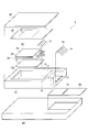
- FIG. 1 is a perspective view showing the liquid crystal display device of the first embodiment.
- FIG. 2 is an exploded view of the liquid crystal display device of the first embodiment.
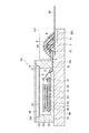
- 3 is a cross-sectional view of the liquid crystal display device taken along AB in FIG.
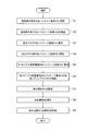
- FIG. 4 is a flowchart for explaining a method of manufacturing the liquid crystal display device of the first and second embodiments.
- FIG. 5 is a cross-sectional view of a liquid crystal display device of a comparative example.
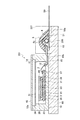
- FIG. 6 is a cross-sectional view of the liquid crystal display device of the second embodiment.
- FIG. 1 shows a configuration example of the liquid crystal display device of the first embodiment.
- FIG. 2 shows each component in a state where the liquid crystal display device is disassembled.
- FIG. 3 shows a cross section of the liquid crystal display device taken along AB in FIG.
- the liquid crystal display device 1 includes a package substrate 10 (first substrate), a liquid crystal display element 20, a light shielding mask 30, a sealing glass plate 40, and a flexible wiring substrate 50 ( A second substrate).
- the package substrate 10 includes a recess 11, a plurality of liquid crystal display element connection terminals 12 (third connection terminals), a plurality of flexible wiring board connection terminals 13 (first connection terminals), and a stepped portion 14.
- the liquid crystal display device 1 is a reflective liquid crystal display device.
- the plurality of liquid crystal display element connection terminals 12 are arranged in the recesses 11.
- the plurality of flexible wiring board connection terminals 13 are arranged on the outer periphery of the package substrate 10.
- the plurality of liquid crystal display element connection terminals 12 and the plurality of flexible wiring board connection terminals 13 are electrically connected to each other via a plurality of internal wirings 15 formed inside the package substrate 10.
- a ceramic package substrate may be used as the package substrate 10.
- the liquid crystal display element 20 is fixed to the recess 11 of the package substrate 10 via the heat conductive adhesive member 2.
- a sheet-like heat conductive gel may be used.
- the liquid crystal display element 20 includes a drive substrate 22 having a plurality of pixel electrodes 21, a transparent substrate 24 having a transparent electrode 23, a liquid crystal 25, and a sealing material 26.
- a silicon substrate may be used as the drive substrate 22.
- a glass plate may be used as the transparent substrate 24.
- the pixel electrode 21 has light reflectivity. Aluminum may be used as the material of the pixel electrode 21.
- the transparent electrode 23 is light transmissive. ITO (indium tin oxide) may be used as the material of the transparent electrode 23.
- the drive substrate 22 and the transparent substrate 24 are bonded by a sealing material 26 so that the pixel electrode 21 and the transparent electrode 23 face each other.
- the sealing material 26 is formed in an annular shape along the outer peripheral portion of the transparent substrate 24.
- the liquid crystal 25 is filled in a gap between the driving substrate 22 and the transparent substrate 24 and sealed with a sealing material 26.
- the drive substrate 22 has a plurality of package substrate connection terminals 27. The plurality of package substrate connection terminals 27 are arranged on the outer peripheral portion of the drive substrate 22.
- the liquid crystal display element 20 and the package substrate 10 are electrically connected via a plurality of bonding wires 3. Specifically, a plurality of package substrate connection terminals 27 of the drive substrate 22 of the liquid crystal display element 20 and a plurality of liquid crystal display element connection terminals 12 of the package substrate 10 are connected via a plurality of bonding wires 3, respectively. Has been. That is, the flexible wiring board connecting terminal 13 of the package substrate 10 is electrically connected to the liquid crystal display element 20.
- the light shielding mask 30 has a light transmission region 31 that transmits light.
- the light shielding mask 30 is fixed to the step portion 14 of the package substrate 10 so that the light transmission region 31 corresponds to a region where the plurality of pixel electrodes 21 are formed.
- the light shielding mask 30 may be fixed to the step portion 14 using an ultraviolet curable resin.
- the sealing glass plate 40 is fixed to the upper surface 10 a (first surface) of the package substrate 10.
- the sealing glass plate 40 may be fixed to the upper surface 10a using a resin that can be used in combination with photocuring (for example, ultraviolet curing) and heat curing.
- photocuring for example, ultraviolet curing
- the liquid crystal display element 20 and the light shielding mask 30 are sealed by the sealing glass plate 40 and the package substrate 10.
- the flexible wiring substrate 50 is fixed to a lower surface 10b (second surface) that is a surface opposite to the upper surface 10a of the package substrate 10. You may make it fix the flexible wiring board 50 to the lower surface 10b using an adhesive agent.
- the flexible wiring board 50 has a package board connection terminal 51 (second connection terminal).
- the flexible wiring substrate 50 and the package substrate 10 are electrically connected via a plurality of bonding wires 4.
- the plurality of package substrate connection terminals 51 of the flexible wiring substrate 50 and the plurality of flexible wiring substrate connection terminals 13 of the package substrate 10 are connected to each other via a plurality of bonding wires 4.
- the plurality of bonding wires 4 are arranged along the arrangement direction of the plurality of package substrate connection terminals 51 and the plurality of flexible wiring substrate connection terminals 13.
- the bonding wire 4 is formed in a state where the flexible wiring substrate 50 is fixed to the package substrate 10.
- the bonding wire 4 has an arcuate loop portion 4a. Gold may be used as the material of the bonding wires 3 and 4.
- the heat sink 60 may be fixed to the lower surface 10b of the package substrate 10 and the lower surface 50b of the flexible wiring substrate 50.
- the heat sink 60 releases the heat generated in the liquid crystal display device 1 to the outside.
- a heat sink formed of an aluminum material may be used as the heat radiating plate 60.
- a sealing resin 6 for sealing the plurality of bonding wires 4 is formed on the package substrate 10 and the flexible wiring substrate 50.
- the sealing resin 6 has a cylindrical cavity 5.
- the cavity 5 is a region between the plurality of flexible wiring board connection terminals 13 of the package substrate 10 and the plurality of package board connection terminals 51 of the flexible wiring board 50, specifically, the loop portion of the plurality of bonding wires 4. It is formed in a region on the center point side of the arc of 4a (region below the loop portion 4a in FIG. 3).
- the cavity 5 is formed such that the central axis of the cavity 5 is parallel to the arrangement direction of the bonding wires 4.
- the liquid crystal display device 1 has a bonding wire resin sealing structure in which a plurality of bonding wires 4 are sealed with a sealing resin 6 and a cavity 5 is formed in a region below the loop portion 4a of the bonding wire 4 7
- the sealing resin 6 is not shown and the cavity 5 is indicated by a broken line.
- illustration of the sealing resin 6 and the cavity 5 is omitted.
- the mechanical stress from the outside to the plurality of bonding wires 4 can be protected by the sealing resin 6. Further, the moisture resistance to the bonding wire 4 can be improved by the sealing resin 6.
- thermosetting resin When a thermosetting resin is used as the sealing resin 6, heating is necessary to cure the sealing resin 6. Since the heat conductive adhesive member 2, the liquid crystal 25, and the adhesive member for fixing the light shielding mask 30 and the sealing glass plate 40 are affected by heating, the performance of each member is deteriorated. Therefore, it is preferable to use an ultraviolet curable resin as the sealing resin 6.
- the image light is reflected by the pixel electrode 21, passes through the light transmission region 31 of the light shielding mask 30 and the sealing glass plate 40, and is emitted to the outside.
- An image can be displayed by projecting image light onto a screen or the like via a projection lens.
- step S ⁇ b> 1 An example of the manufacturing method of the liquid crystal display device 1 including the bonding wire resin sealing method will be described using the flowchart of FIG.
- step S ⁇ b> 1 the operator fixes the liquid crystal display element 20 to the recess 11 of the package substrate 10 via the heat conductive adhesive member 2.
- step S2 the operator connects the plurality of package substrate connection terminals 27 of the drive substrate 22 and the plurality of liquid crystal display element connection terminals 12 of the package substrate 10 via the plurality of bonding wires 3, respectively. Thereby, the drive substrate 22 and the package substrate 10 constituting the liquid crystal display element 20 are electrically connected via the bonding wires 3.
- step S3 the operator fixes the light shielding mask 30 to the stepped portion 14 of the package substrate 10 so that the light transmission region 31 corresponds to the region where the plurality of pixel electrodes 21 are formed.
- the operator fixes the sealing glass plate 40 to the upper surface 10a of the package substrate 10 in step S4. Thereby, the liquid crystal display element 20 and the light shielding mask 30 are sealed by the sealing glass plate 40 and the package substrate 10.
- the operator fixes the flexible wiring board 50 to the lower surface 10b of the package board 10 in step S5.
- a heat sink for releasing the heat generated in the liquid crystal display device 1 to the outside may be fixed to the lower surface 10b of the package substrate 10.
- step S ⁇ b> 6 the operator connects the plurality of package substrate connection terminals 51 of the flexible wiring substrate 50 and the plurality of flexible wiring substrate connection terminals 13 of the package substrate 10 via the plurality of bonding wires 4. .
- step S ⁇ b> 7 the operator is an area between the plurality of flexible wiring board connection terminals 13 of the package substrate 10 and the plurality of package board connection terminals 51 of the flexible wiring board 50, and the plurality of bonding wires 4.
- a rod-shaped member 501 for forming the hollow portion 5 is disposed in a region on the center point side of the arc of the loop portion 4 a so that the central axis of the rod-shaped member 501 is parallel to the arrangement direction of the bonding wires 4. Note that the rod-shaped member 501 may be disposed before the bonding wire 4 is formed.
- step S ⁇ b> 8 the operator applies the sealing resin 6, which is an ultraviolet curable resin, so as to seal the plurality of bonding wires 4 and the rod-shaped member 501 on the package substrate 10 and the flexible wiring substrate 50. .
- the operator irradiates the sealing resin 6 with ultraviolet rays to cure the sealing resin 6.
- the operator removes the rod-shaped member 501 from the sealing resin 6 in step S9. Specifically, the rod-shaped member 501 is moved in the central axis direction and pulled out from the sealing resin 6. Since the sealing resin 6 contracts when cured, the rod-shaped member 501 can be pulled out from the sealing resin 6. In order to make it easy to pull out the rod-shaped member 501, it is preferable to form the rod-shaped member 501 with a material having a small adhesion to the sealing resin 6. A fluororesin rod having a circular cross section may be used as the rod-shaped member 501.
- a region where the rod-shaped member 501 is pulled out from the sealing resin 6 becomes the cavity 5. That is, by pulling out the rod-shaped member 501 from the sealing resin 6, the cavity 5 corresponding to the shape of the rod-shaped member 501 is formed in the sealing resin 6.
- the sealing resin 6 may be irradiated with ultraviolet rays to add a step of curing the sealing resin 6. After the sealing resin 6 is cured, the heat sink 60 may be fixed to the lower surface 10 b of the package substrate 10 and the lower surface 50 b of the flexible wiring substrate 50.
- the bonding wire resin sealing structure 7 is formed in which the plurality of bonding wires 4 are sealed with the sealing resin 6 and the cavity 5 is formed in the region below the loop portion 4a of the bonding wire 4.
- the liquid crystal display device 1 is produced. Note that steps S1 to S9 may be executed using a manufacturing apparatus.
- FIG. 5 shows a bonding wire resin sealing structure and a liquid crystal display device of a comparative example for comparison with the bonding wire resin sealing structure 7 and the liquid crystal display device 1 of the first embodiment.
- FIG. 5 corresponds to FIG.
- the same components as those of the bonding wire resin sealing structure 7 and the liquid crystal display device 1 of the first embodiment are denoted by the same reference numerals.
- the liquid crystal display device 101 of the comparative example has a bonding wire resin sealing structure 107 in which a plurality of bonding wires 4 are covered with a sealing resin 6. That is, the bonding wire resin sealing structure 107 and the liquid crystal display device 101 of the comparative example have the cavity 5 in the sealing resin 6 as compared with the bonding wire resin sealing structure 7 and the liquid crystal display device 1 of the first embodiment. It is different in that it is not formed, and is otherwise the same.
- a displacement difference is generated according to the difference between the thermal expansion coefficient of the package substrate 10 and the thermal expansion coefficient of the sealing resin 6.
- the thermal expansion coefficient of the package substrate 10 is about 7 ⁇ 10 ⁇ 6 / K.
- the thermal expansion coefficient of the sealing resin 6 is about 300 ⁇ 10 ⁇ 6 / K.
- the bonding wire 4 When the load according to the displacement difference is applied to the bonding wire 4 in the direction of the outside of the sealing resin 6, the bonding wire 4 may be disconnected. Specifically, the wire may be disconnected at the wire neck portion of the bonding wire 4 connected to the flexible wiring board connecting terminal 13. As an example of the thermal shock test conditions, the environmental temperature is periodically changed between ⁇ 40 ° C. and 85 ° C.
- the sealing resin 6 has the cavity 5 formed in the region below the loop portion 4a of the bonding wire 4. Yes.
- the thickness of the sealing resin 6 for sealing the bonding wire 4 is reduced with respect to the bonding wire resin sealing structure 107 and the liquid crystal display device 101 of the comparative example. be able to. Thereby, a displacement difference can be made small.
- the load applied to the bonding wire 4 can be dispersed in the direction toward the outside of the sealing resin 6 and the direction toward the inside of the cavity 5. .
- the load applied to the bonding wire 4 can be reduced and dispersed by the cavity 5 formed in the sealing resin 6. Reliability can be ensured even in harsh environments.
- the rod-shaped member 501 for forming the cavity 5 may be any shape and size that does not contact the bonding wire 4.
- the rod-shaped member 501 may have a tapered shape whose diameter continuously or intermittently decreases in a direction opposite to the direction in which the rod-shaped member 501 is pulled out from the sealing resin 6. By making the rod-shaped member 501 tapered, the rod-shaped member 501 can be easily pulled out from the sealing resin 6.
- FIG. 6 shows a state in which the liquid crystal display device 201 according to the second embodiment having the hollow portion 205 formed of a tapered rod-like member is viewed from the side from which the rod-like member is pulled out.
- the liquid crystal display device 201 includes the bonding wire resin sealing structure 207 of the second embodiment in which the bonding wire 4 is sealed with a sealing resin 6 having a hollow portion 205 formed of a tapered rod-shaped member.
- the cavity 205 formed by the tapered rod-shaped member is formed so that the central axis of the cavity 205 is parallel to the arrangement direction of the bonding wires 4.
- the hollow portion 205 has a truncated cone shape whose diameter increases in the direction in which the rod-shaped member is pulled out.
Landscapes
- Physics & Mathematics (AREA)
- Nonlinear Science (AREA)
- General Physics & Mathematics (AREA)
- Liquid Crystal (AREA)
- Engineering & Computer Science (AREA)
- Mathematical Physics (AREA)
- Chemical & Material Sciences (AREA)
- Crystallography & Structural Chemistry (AREA)
- Optics & Photonics (AREA)
- Theoretical Computer Science (AREA)
- Microelectronics & Electronic Packaging (AREA)
- Combinations Of Printed Boards (AREA)
- Encapsulation Of And Coatings For Semiconductor Or Solid State Devices (AREA)
- Devices For Indicating Variable Information By Combining Individual Elements (AREA)
- Structures Or Materials For Encapsulating Or Coating Semiconductor Devices Or Solid State Devices (AREA)
Abstract
ボンディングワイヤ樹脂封止構造(7)は、第1の基板(10)と第2の基板(50)とボンディングワイヤ(4)と封止樹脂(6)と空洞部(5)とを備える。第1の基板(10)は第1の接続端子(13)を有する。第2の基板(50)は第1の基板(10)に固定され、第2の接続端子(51)を有する。ボンディングワイヤ(4)は円弧状のループ部(4a)を有し、第1の接続端子(13)と第2の接続端子(51)とを接続する。封止樹脂(6)は第1及び第2の基板(10及び50)上に形成され、ボンディングワイヤ(4)を封止する。空洞部(5)は、封止樹脂(6)における、第1の接続端子(13)と第2の接続端子(51)との間の領域であり、かつ、ループ部(4a)の円弧の中心点側の領域に形成されている。
Description
本開示は、ボンディングワイヤ樹脂封止構造、液晶表示デバイス、及びボンディングワイヤ樹脂封止方法に関する。
液晶表示デバイスは、プロジェクタまたはヘッドアップディスプレイ等の表示装置に用いられている。液晶表示デバイスは、照射された照明光を画素毎に光変調して画像光を生成する。表示装置は、液晶表示デバイスにより生成された画像光をスクリーン等に投射することにより、画像を表示する。特許文献1には液晶表示デバイスの一例が記載されている。
液晶表示デバイスは、パッケージ基板とフレキシブル配線板とが複数のボンディングワイヤにより接続されている。複数のボンディングワイヤは互いが接触しないように樹脂で封止されている。車載用の液晶表示デバイスでは、過酷な環境でも信頼性を確保できるように、熱サイクル試験や熱衝撃試験等の厳しい信頼性条件を満足することが必要である。
しかしながら、熱サイクル試験や熱衝撃試験では、封止樹脂の熱膨張係数とパッケージ基板の熱膨張係数との差によって変位差が生じる。ボンディングワイヤには、変位差に応じて負荷がかかるため、変位差が大きいとボンディングワイヤを断線させる場合がある。
実施形態は、ボンディングワイヤを断線させる要因となる熱膨張係数の差によって生じる変位差を低減させることにより、過酷な環境でも信頼性を確保できるボンディングワイヤ樹脂封止構造、液晶表示デバイス、及びボンディングワイヤ樹脂封止方法を提供することを目的とする。
実施形態の第1の態様によれば、第1の接続端子を有する第1の基板と、前記第1の基板に固定され、第2の接続端子を有する第2の基板と、前記第1の接続端子と前記第2の接続端子とを接続する、円弧状のループ部を有するボンディングワイヤと、前記第1の基板上及び前記第2の基板上に形成され、前記ボンディングワイヤを封止する封止樹脂とを備え、前記封止樹脂における、前記第1の接続端子と前記第2の接続端子との間の領域であり、かつ、前記ループ部の円弧の中心点側の領域には、空洞部が形成されていることを特徴とするボンディングワイヤ樹脂封止構造が提供される。
実施形態の第2の態様によれば、液晶表示素子と、第1の接続端子を有する第1の基板と、前記第1の基板に固定され、第2の接続端子を有する第2の基板とを備え、前記第1の基板は、前記液晶表示素子及び前記第1の接続端子と接続された第3の接続端子を有し、前記第1の接続端子と前記第2の接続端子とを接続する、円弧状のループ部を有するボンディングワイヤと、前記第1の基板上及び前記第2の基板上に形成され、前記ボンディングワイヤを封止する封止樹脂とをさらに備え、前記封止樹脂における、前記第1の接続端子と前記第2の接続端子との間の領域であり、かつ、前記ループ部の円弧の中心点側の領域には、空洞部が形成されていることを特徴とする液晶表示デバイスが提供される。
実施形態の第3の態様によれば、第1の接続端子を有する第1の基板に、第2の接続端子を有する第2の基板を固定し、前記第1の接続端子と前記第2の接続端子とを、円弧状のループ部を有するボンディングワイヤで接続し、前記第1の接続端子と前記第2の接続端子との間の領域であり、かつ、前記ループ部の円弧の中心点側の領域に、棒状部材を配置し、前記第1の基板上及び前記第2の基板上に、前記ボンディングワイヤ及び前記棒状部材を封止する封止樹脂を形成し、前記封止樹脂から前記棒状部材を除去し、前記封止樹脂に前記棒状部材の形状に対応する空洞部を形成することを特徴とするボンディングワイヤ樹脂封止方法が提供される。
実施形態のボンディングワイヤ樹脂封止構造、液晶表示デバイス、及びボンディングワイヤ樹脂封止方法によれば、ボンディングワイヤを断線させる要因となる熱膨張係数の差によって生じる変位差を低減させることにより、過酷な環境でも信頼性を確保することができる。
図1~図3を用いて、第1実施形態のボンディングワイヤ樹脂封止構造及び液晶表示デバイスを説明する。図1は第1実施形態の液晶表示デバイスの構成例を示している。図2は液晶表示デバイスを分解した状態の各構成部を示している。図3は図1のA-Bを通る液晶表示デバイスの断面を示している。
図1または図2に示すように、液晶表示デバイス1は、パッケージ基板10(第1の基板)と、液晶表示素子20と、遮光マスク30と、封止ガラス板40と、フレキシブル配線基板50(第2の基板)とを備える。パッケージ基板10は、凹部11と、複数の液晶表示素子接続用端子12(第3の接続端子)と、複数のフレキシブル配線基板接続用端子13(第1の接続端子)と、段部14とを有する。液晶表示デバイス1は、反射型の液晶表示デバイスである。
図3に示すように、複数の液晶表示素子接続用端子12は凹部11に配列されている。複数のフレキシブル配線基板接続用端子13は、パッケージ基板10の外周部に配列されている。複数の液晶表示素子接続用端子12と複数のフレキシブル配線基板接続用端子13とは、パッケージ基板10の内部に形成された複数の内部配線15を介してそれぞれ電気的に接続されている。パッケージ基板10として、セラミックパッケージ基板を用いてもよい。
液晶表示素子20は、熱伝導性接着部材2を介して、パッケージ基板10の凹部11に固定されている。熱伝導性接着部材2として、シート状の熱伝導性ゲルを用いてもよい。液晶表示素子20は、複数の画素電極21を有する駆動基板22と、透明電極23を有する透明基板24と、液晶25と、シール材26とを有する。
駆動基板22としてシリコン基板を用いてもよい。透明基板24としてガラス板を用いてもよい。画素電極21は光反射性を有する。画素電極21の材料としてアルミニウムを用いてもよい。透明電極23は光透過性を有する。透明電極23の材料としてITO(酸化インジウム錫)を用いてもよい。
駆動基板22と透明基板24とは、画素電極21と透明電極23とが対向するようにシール材26により接着されている。シール材26は透明基板24の外周部に沿って環状に形成されている。液晶25は、駆動基板22と透明基板24との間隙に充填され、シール材26により封止されている。駆動基板22は、複数のパッケージ基板接続用端子27を有する。複数のパッケージ基板接続用端子27は、駆動基板22の外周部に配列されている。
液晶表示素子20とパッケージ基板10とは、複数のボンディングワイヤ3を介して電気的に接続されている。具体的には、液晶表示素子20の駆動基板22の複数のパッケージ基板接続用端子27と、パッケージ基板10の複数の液晶表示素子接続用端子12とが、複数のボンディングワイヤ3を介してそれぞれ接続されている。即ち、パッケージ基板10のフレキシブル配線基板接続用端子13は、液晶表示素子20と電気的に接続されている。
遮光マスク30は、光を透過する光透過領域31を有する。遮光マスク30は、光透過領域31が複数の画素電極21が形成されている領域に対応するように、パッケージ基板10の段部14に固定されている。遮光マスク30を紫外線硬化性樹脂を用いて段部14に固定するようにしてもよい。
封止ガラス板40は、パッケージ基板10の上面10a(第1の面)に固定されている。封止ガラス板40を、光硬化(例えば紫外線硬化)と熱硬化との併用が可能な樹脂を用いて上面10aに固定するようにしてもよい。液晶表示素子20及び遮光マスク30は、封止ガラス板40とパッケージ基板10とにより密閉されている。
フレキシブル配線基板50は、パッケージ基板10の上面10aとは反対側の面である下面10b(第2の面)に固定されている。フレキシブル配線基板50を接着剤を用いて下面10bに固定するようにしてもよい。フレキシブル配線基板50は、パッケージ基板接続用端子51(第2の接続端子)を有する。
フレキシブル配線基板50とパッケージ基板10とは、複数のボンディングワイヤ4を介して電気的に接続されている。具体的には、フレキシブル配線基板50の複数のパッケージ基板接続用端子51と、パッケージ基板10の複数のフレキシブル配線基板接続用端子13とは、複数のボンディングワイヤ4を介してそれぞれ接続されている。複数のボンディングワイヤ4は、複数のパッケージ基板接続用端子51及び複数のフレキシブル配線基板接続用端子13の配列方向に沿って配列されている。
ボンディングワイヤ4は、フレキシブル配線基板50がパッケージ基板10に固定されている状態で形成される。ボンディングワイヤ4は、円弧状のループ部4aを有する。ボンディングワイヤ3,4の材料として金を用いてもよい。
パッケージ基板10の下面10b及びフレキシブル配線基板50の下面50bに放熱板60を固定するようにしてもよい。放熱板60は、液晶表示デバイス1で発生した熱を外部へ放出する。放熱板60として、アルミニウム材により形成されたヒートシンクを用いてもよい。
パッケージ基板10上及びフレキシブル配線基板50上には、複数のボンディングワイヤ4を封止する封止樹脂6が形成されている。封止樹脂6は筒状の空洞部5を有する。空洞部5は、パッケージ基板10の複数のフレキシブル配線基板接続用端子13とフレキシブル配線基板50の複数のパッケージ基板接続用端子51との間の領域、具体的には複数のボンディングワイヤ4のループ部4aの円弧の中心点側の領域(図3におけるループ部4aの下側の領域)に形成されている。空洞部5は、空洞部5の中心軸がボンディングワイヤ4の配列方向と平行になるように形成されている。
液晶表示デバイス1は、複数のボンディングワイヤ4が封止樹脂6で封止され、かつ、ボンディングワイヤ4のループ部4aの下側の領域に空洞部5が形成されているボンディングワイヤ樹脂封止構造7を有する。なお、図1では、ボンディングワイヤ4と空洞部5との位置関係をわかりやすくするために、封止樹脂6の図示を省略し、空洞部5を破線で示している。図2では、封止樹脂6及び空洞部5の図示を省略している。
複数のボンディングワイヤ4に対する外部からの機械的ストレスを封止樹脂6により保護することができる。また、ボンディングワイヤ4に対する耐湿性を封止樹脂6により向上させることができる。
封止樹脂6として熱硬化性樹脂を用いる場合、封止樹脂6を硬化させるためには加熱することが必要である。熱伝導性接着部材2、液晶25、並びに、遮光マスク30及び封止ガラス板40を固定するための接着部材が加熱による影響を受けるため、各部材の性能を悪化させる要因となる。そのため、封止樹脂6として紫外線硬化性樹脂を用いることが好ましい。
外部から画像データがフレキシブル配線基板50及びパッケージ基板10を介して液晶表示素子20へ入力されることにより、画像データに基づく駆動電圧が画素電極21毎に印加される。外部から照明光が封止ガラス板40及び遮光マスク30の光透過領域31を透過して液晶表示素子20に照射されることにより、照明光は液晶表示素子20により光変調され、画像光が生成される。
画像光は、画素電極21により反射され、遮光マスク30の光透過領域31及び封止ガラス板40を透過して外部へ射出される。画像光を投射レンズを介してスクリーン等へ投射させることにより、画像を表示することができる。
図4のフローチャートを用いて、ボンディングワイヤ樹脂封止方法を含む、液晶表示デバイス1の製造方法の一例を説明する。オペレータは、ステップS1にて、液晶表示素子20を、熱伝導性接着部材2を介して、パッケージ基板10の凹部11に固定する。
オペレータは、ステップS2にて、駆動基板22の複数のパッケージ基板接続用端子27と、パッケージ基板10の複数の液晶表示素子接続用端子12とを、複数のボンディングワイヤ3を介してそれぞれ接続する。これにより、液晶表示素子20を構成する駆動基板22とパッケージ基板10とは、ボンディングワイヤ3を介して電気的に接続される。
オペレータは、ステップS3にて、遮光マスク30を、光透過領域31が複数の画素電極21が形成されている領域に対応するように、パッケージ基板10の段部14に固定する。オペレータは、ステップS4にて、封止ガラス板40を、パッケージ基板10の上面10aに固定する。これにより、液晶表示素子20及び遮光マスク30は、封止ガラス板40とパッケージ基板10とにより密閉される。
オペレータは、ステップS5にて、フレキシブル配線基板50を、パッケージ基板10の下面10bに固定する。なお、フレキシブル配線基板50を固定した後に、パッケージ基板10の下面10bに、液晶表示デバイス1で発生した熱を外部へ放出するためのヒートシンクを固定するようにしてもよい。
オペレータは、ステップS6にて、フレキシブル配線基板50の複数のパッケージ基板接続用端子51と、パッケージ基板10の複数のフレキシブル配線基板接続用端子13とを、複数のボンディングワイヤ4を介してそれぞれ接続する。
オペレータは、ステップS7にて、パッケージ基板10の複数のフレキシブル配線基板接続用端子13とフレキシブル配線基板50の複数のパッケージ基板接続用端子51との間の領域であり、かつ、複数のボンディングワイヤ4のループ部4aの円弧の中心点側の領域に、空洞部5を形成するための棒状部材501を、棒状部材501の中心軸がボンディングワイヤ4の配列方向と平行になるように配置する。なお、棒状部材501をボンディングワイヤ4が形成される前に配置してもよい。
オペレータは、ステップS8にて、パッケージ基板10上及びフレキシブル配線基板50上に、複数のボンディングワイヤ4と棒状部材501とを封止するように、紫外線硬化性樹脂である封止樹脂6を塗布する。オペレータは、封止樹脂6に紫外線を照射し、封止樹脂6を硬化させる。
オペレータは、ステップS9にて、棒状部材501を封止樹脂6から除去する。具体的には、棒状部材501を中心軸方向に移動させて封止樹脂6から引き抜く。封止樹脂6は、硬化することにより収縮するため、棒状部材501を封止樹脂6から引き抜くことができる。棒状部材501を引き抜きやすくするため、棒状部材501を封止樹脂6との密着力が小さい材料で形成することが好ましい。棒状部材501として断面形状が円形のフッ素樹脂棒を用いてもよい。
封止樹脂6から棒状部材501が引き抜かれた領域が空洞部5となる。即ち、封止樹脂6から棒状部材501が引き抜かれることにより、封止樹脂6に棒状部材501の形状に対応する空洞部5が形成される。なお、空洞部5が形成された後に、封止樹脂6に紫外線を照射して封止樹脂6の硬化工程を追加するようにしてもよい。封止樹脂6を硬化させた後に、パッケージ基板10の下面10b及びフレキシブル配線基板50の下面50bに放熱板60を固定するようにしてもよい。
これにより、複数のボンディングワイヤ4が封止樹脂6で封止され、かつ、ボンディングワイヤ4のループ部4aの下側の領域に空洞部5が形成されているボンディングワイヤ樹脂封止構造7を有する液晶表示デバイス1が作製される。なお、ステップS1~ステップS9を製造装置を用いて実行してもよい。
図5は、第1実施形態のボンディングワイヤ樹脂封止構造7及び液晶表示デバイス1と比較するための比較例のボンディングワイヤ樹脂封止構造及び液晶表示デバイスを示している。図5は図3に対応する。説明をわかりやすくするために、第1実施形態のボンディングワイヤ樹脂封止構造7及び液晶表示デバイス1と同じ構成部には同じ符号を付す。
図5に示すように、比較例の液晶表示デバイス101は、複数のボンディングワイヤ4が封止樹脂6で覆われたボンディングワイヤ樹脂封止構造107を有する。即ち、比較例のボンディングワイヤ樹脂封止構造107及び液晶表示デバイス101は、第1実施形態のボンディングワイヤ樹脂封止構造7及び液晶表示デバイス1と比較して、封止樹脂6に空洞部5が形成されていない点で相違し、それ以外は同じである。
比較例の液晶表示デバイス101に対して熱衝撃試験を実行すると、パッケージ基板10の熱膨張係数と封止樹脂6の熱膨張係数との差に応じて変位差が生じる。パッケージ基板10としてセラミックパッケージ基板を用いた場合、パッケージ基板10の熱膨張係数は約7×10⁻⁶/Kである。封止樹脂6として紫外線硬化性樹脂を用いた場合、封止樹脂6の熱膨張係数は約300×10-6/Kである。
変位差に応じた負荷が、ボンディングワイヤ4に対して封止樹脂6の外側の方向に加わることにより、ボンディングワイヤ4が断線する場合がある。具体的には、ボンディングワイヤ4のフレキシブル配線基板接続用端子13に接続するワイヤネック部分で断線する場合がある。熱衝撃試験条件の一例として、環境温度を-40℃と85℃とに周期的に変化させる。
それに対して、第1実施形態のボンディングワイヤ樹脂封止構造7及び液晶表示デバイス1では、封止樹脂6には、ボンディングワイヤ4のループ部4aの下側の領域に空洞部5が形成されている。封止樹脂6に空洞部5を形成することにより、比較例のボンディングワイヤ樹脂封止構造107及び液晶表示デバイス101に対して、ボンディングワイヤ4を封止する封止樹脂6の厚さを薄くすることができる。これにより、変位差を小さくすることができる。また、封止樹脂6に空洞部5を形成することにより、ボンディングワイヤ4に加わる負荷を、封止樹脂6の外側に向かう方向と、空洞部5の内側に向かう方向とに分散させることができる。
従って、ボンディングワイヤ樹脂封止構造7及び液晶表示デバイス1によれば、ボンディングワイヤ4に加わる負荷を、封止樹脂6に形成された空洞部5により小さくし、かつ、分散させることができるので、過酷な環境でも信頼性を確保することができる。
なお、本発明は、上述した第1実施形態の構成に限定されるものではなく、本発明の要旨を逸脱しない範囲において種々変更可能である。例えば、空洞部5を形成するための棒状部材501は、ボンディングワイヤ4に接触しない形状及び大きさであればよい。
棒状部材501を、封止樹脂6から引き抜く方向とは反対方向に直径が連続的または断続的に小さくなるような先細り形状としてもよい。棒状部材501を先細り形状にすることにより、棒状部材501を封止樹脂6から引き抜きやすくことができる。
図6は、先細り形状の棒状部材により形成された空洞部205を有する第2実施形態の液晶表示デバイス201を、棒状部材が引き抜かれた側から見た状態を示している。液晶表示デバイス201は、先細り形状の棒状部材により形成された空洞部205を有する封止樹脂6によってボンディングワイヤ4を封止する第2実施形態のボンディングワイヤ樹脂封止構造207を備える。先細り形状の棒状部材により形成された空洞部205は、空洞部205の中心軸がボンディングワイヤ4の配列方向と平行になるように形成されている。また、空洞部205は、棒状部材が引き抜かれる方向に直径が大きくなる円錐台形状を有する。
本願の開示は、2017年2月21日に出願された特願2017-030055号に記載の主題と関連しており、それらの全ての開示内容は引用によりここに援用される。
既に述べられたもの以外に、本発明の新規かつ有利な特徴から外れることなく、上記の実施形態に様々な修正や変更を加えてもよいことに注意すべきである。従って、そのような全ての修正や変更は、添付の請求の範囲に含まれることが意図されている。
既に述べられたもの以外に、本発明の新規かつ有利な特徴から外れることなく、上記の実施形態に様々な修正や変更を加えてもよいことに注意すべきである。従って、そのような全ての修正や変更は、添付の請求の範囲に含まれることが意図されている。
Claims (5)
- 第1の接続端子を有する第1の基板と、
前記第1の基板に固定され、第2の接続端子を有する第2の基板と、
前記第1の接続端子と前記第2の接続端子とを接続する、円弧状のループ部を有するボンディングワイヤと、
前記第1の基板上及び前記第2の基板上に形成され、前記ボンディングワイヤを封止する封止樹脂と、
を備え、
前記封止樹脂における、前記第1の接続端子と前記第2の接続端子との間の領域であり、かつ、前記ループ部の円弧の中心点側の領域には、空洞部が形成されている
ことを特徴とするボンディングワイヤ樹脂封止構造。 - 前記第1の基板は、複数の前記第1の接続端子を有し、
前記第2の基板は、複数の前記第2の接続端子を有し、
前記複数の第1の接続端子と前記複数の第2の接続端子とは、複数の前記ボンディングワイヤを介してそれぞれ接続され、
前記空洞部は、筒状の形状を有し、前記空洞部の中心軸と前記ボンディングワイヤが配列されている方向とが平行になるように形成されている
ことを特徴とする請求項1に記載のボンディングワイヤ樹脂封止構造。 - 液晶表示素子と、
第1の接続端子を有する第1の基板と、
前記第1の基板に固定され、第2の接続端子を有する第2の基板と、
を備え、
前記第1の基板は、前記液晶表示素子及び前記第1の接続端子と接続された第3の接続端子を有し、
前記第1の接続端子と前記第2の接続端子とを接続する、円弧状のループ部を有するボンディングワイヤと、
前記第1の基板上及び前記第2の基板上に形成され、前記ボンディングワイヤを封止する封止樹脂と、
をさらに備え、
前記封止樹脂における、前記第1の接続端子と前記第2の接続端子との間の領域であり、かつ、前記ループ部の円弧の中心点側の領域には、空洞部が形成されている
ことを特徴とする液晶表示デバイス。 - 前記第1の基板は、複数の前記第1の接続端子を有し、
前記第2の基板は、複数の前記第2の接続端子を有し、
前記複数の第1の接続端子と前記複数の第2の接続端子とは、複数の前記ボンディングワイヤを介してそれぞれ接続され、
前記空洞部は、筒状の形状を有し、前記空洞部の中心軸と前記ボンディングワイヤが配列されている方向とが平行になるように形成されている
ことを特徴とする請求項3に記載の液晶表示デバイス。 - 第1の接続端子を有する第1の基板に、第2の接続端子を有する第2の基板を固定し、
前記第1の接続端子と前記第2の接続端子とを、円弧状のループ部を有するボンディングワイヤで接続し、
前記第1の接続端子と前記第2の接続端子との間の領域であり、かつ、前記ループ部の円弧の中心点側の領域に、棒状部材を配置し、
前記第1の基板上及び前記第2の基板上に、前記ボンディングワイヤ及び前記棒状部材を封止する封止樹脂を形成し、
前記封止樹脂から前記棒状部材を除去し、前記封止樹脂に前記棒状部材の形状に対応する空洞部を形成する
ことを特徴とするボンディングワイヤ樹脂封止方法。
Applications Claiming Priority (2)
| Application Number | Priority Date | Filing Date | Title |
|---|---|---|---|
| JP2017030055A JP6784191B2 (ja) | 2017-02-21 | 2017-02-21 | ボンディングワイヤ樹脂封止構造、液晶表示デバイス、及びボンディングワイヤ樹脂封止方法 |
| JP2017-030055 | 2017-02-21 |
Publications (1)
| Publication Number | Publication Date |
|---|---|
| WO2018154835A1 true WO2018154835A1 (ja) | 2018-08-30 |
Family
ID=63254356
Family Applications (1)
| Application Number | Title | Priority Date | Filing Date |
|---|---|---|---|
| PCT/JP2017/036302 Ceased WO2018154835A1 (ja) | 2017-02-21 | 2017-10-05 | ボンディングワイヤ樹脂封止構造、液晶表示デバイス、及びボンディングワイヤ樹脂封止方法 |
Country Status (2)
| Country | Link |
|---|---|
| JP (1) | JP6784191B2 (ja) |
| WO (1) | WO2018154835A1 (ja) |
Citations (3)
| Publication number | Priority date | Publication date | Assignee | Title |
|---|---|---|---|---|
| JPS6353956A (ja) * | 1986-08-25 | 1988-03-08 | Hitachi Ltd | 半導体装置 |
| JP2001118864A (ja) * | 1999-10-15 | 2001-04-27 | Hitachi Chem Co Ltd | 半導体装置の製造方法及びそれにより得られた半導体装置 |
| JP2006267413A (ja) * | 2005-03-23 | 2006-10-05 | Victor Co Of Japan Ltd | 反射型液晶表示素子 |
-
2017
- 2017-02-21 JP JP2017030055A patent/JP6784191B2/ja active Active
- 2017-10-05 WO PCT/JP2017/036302 patent/WO2018154835A1/ja not_active Ceased
Patent Citations (3)
| Publication number | Priority date | Publication date | Assignee | Title |
|---|---|---|---|---|
| JPS6353956A (ja) * | 1986-08-25 | 1988-03-08 | Hitachi Ltd | 半導体装置 |
| JP2001118864A (ja) * | 1999-10-15 | 2001-04-27 | Hitachi Chem Co Ltd | 半導体装置の製造方法及びそれにより得られた半導体装置 |
| JP2006267413A (ja) * | 2005-03-23 | 2006-10-05 | Victor Co Of Japan Ltd | 反射型液晶表示素子 |
Also Published As
| Publication number | Publication date |
|---|---|
| JP2018136409A (ja) | 2018-08-30 |
| JP6784191B2 (ja) | 2020-11-11 |
Similar Documents
| Publication | Publication Date | Title |
|---|---|---|
| JP6404150B2 (ja) | 表示装置の製造方法 | |
| JP5123931B2 (ja) | タッチパネルおよびタッチパネル型表示装置 | |
| JP6379616B2 (ja) | 電気光学装置及び電子機器 | |
| JP5875313B2 (ja) | 電子部品および電子機器ならびにこれらの製造方法。 | |
| US9817157B2 (en) | Lens array substrate, electro-optical apparatus and electronic equipment | |
| CN101743528A (zh) | 触摸面板及触摸面板型显示装置 | |
| US9823438B2 (en) | Electro-optical device, manufacturing method of electro-optical device, and electronic apparatus | |
| WO2016088615A1 (ja) | 湾曲型表示パネルの製造方法 | |
| JP2014134653A (ja) | 表示装置及び電子機器 | |
| US10025008B2 (en) | Method of manufacturing lens array substrate, lens array substrate, electro-optical apparatus, and electronic equipment | |
| JP2018136410A (ja) | 液晶表示デバイス及び液晶表示デバイスの製造方法 | |
| JP2015034865A (ja) | 液晶表示デバイス及びその製造方法 | |
| JP2021047311A (ja) | 電気光学装置および電子機器 | |
| WO2018154835A1 (ja) | ボンディングワイヤ樹脂封止構造、液晶表示デバイス、及びボンディングワイヤ樹脂封止方法 | |
| JP2008250120A (ja) | 液晶表示素子 | |
| JP2018136408A (ja) | ボンディングワイヤ樹脂封止構造、液晶表示デバイス、及びボンディングワイヤ樹脂封止方法 | |
| JP2007249014A (ja) | 液晶表示装置 | |
| JP2018136407A (ja) | ボンディングワイヤ樹脂封止構造及び液晶表示デバイス | |
| CN107238925B (zh) | 电光装置、电光单元及电子设备 | |
| JP7122940B2 (ja) | 液晶表示装置及びその製造方法 | |
| US11199747B2 (en) | Electro-optical device and electronic apparatus | |
| JP6709136B2 (ja) | 液晶表示装置 | |
| JP2009008711A (ja) | 液晶表示素子 | |
| JP2014071341A (ja) | 表示素子及び製造方法 | |
| JP2011008084A (ja) | 投射型表示デバイス |
Legal Events
| Date | Code | Title | Description |
|---|---|---|---|
| 121 | Ep: the epo has been informed by wipo that ep was designated in this application |
Ref document number: 17897488 Country of ref document: EP Kind code of ref document: A1 |
|
| NENP | Non-entry into the national phase |
Ref country code: DE |
|
| 122 | Ep: pct application non-entry in european phase |
Ref document number: 17897488 Country of ref document: EP Kind code of ref document: A1 |