WO2018139767A9 - 신규한 아민계 화합물 및 이를 이용한 유기발광 소자 - Google Patents
신규한 아민계 화합물 및 이를 이용한 유기발광 소자 Download PDFInfo
- Publication number
- WO2018139767A9 WO2018139767A9 PCT/KR2017/015256 KR2017015256W WO2018139767A9 WO 2018139767 A9 WO2018139767 A9 WO 2018139767A9 KR 2017015256 W KR2017015256 W KR 2017015256W WO 2018139767 A9 WO2018139767 A9 WO 2018139767A9
- Authority
- WO
- WIPO (PCT)
- Prior art keywords
- group
- compound
- substituted
- unsubstituted
- layer
- Prior art date
Links
- 150000001875 compounds Chemical class 0.000 title claims abstract description 95
- 150000001412 amines Chemical class 0.000 title abstract description 3
- -1 cyano, nitro, methyl Chemical group 0.000 claims description 36
- 125000003118 aryl group Chemical group 0.000 claims description 30
- 238000000034 method Methods 0.000 claims description 22
- 238000002347 injection Methods 0.000 claims description 21
- 239000007924 injection Substances 0.000 claims description 21
- 230000000903 blocking effect Effects 0.000 claims description 19
- 229910052739 hydrogen Inorganic materials 0.000 claims description 18
- 239000001257 hydrogen Substances 0.000 claims description 18
- 125000000217 alkyl group Chemical group 0.000 claims description 17
- 230000005525 hole transport Effects 0.000 claims description 17
- 125000005842 heteroatom Chemical group 0.000 claims description 12
- YZCKVEUIGOORGS-OUBTZVSYSA-N Deuterium Chemical compound [2H] YZCKVEUIGOORGS-OUBTZVSYSA-N 0.000 claims description 11
- UFHFLCQGNIYNRP-UHFFFAOYSA-N Hydrogen Chemical compound [H][H] UFHFLCQGNIYNRP-UHFFFAOYSA-N 0.000 claims description 11
- 229910052736 halogen Inorganic materials 0.000 claims description 11
- 150000002367 halogens Chemical class 0.000 claims description 11
- 230000032258 transport Effects 0.000 claims description 11
- 125000000623 heterocyclic group Chemical group 0.000 claims description 10
- 229910052757 nitrogen Inorganic materials 0.000 claims description 10
- 229910052717 sulfur Inorganic materials 0.000 claims description 10
- 125000003342 alkenyl group Chemical group 0.000 claims description 9
- 125000004093 cyano group Chemical group *C#N 0.000 claims description 9
- 125000001072 heteroaryl group Chemical group 0.000 claims description 9
- 150000002894 organic compounds Chemical class 0.000 claims description 9
- 125000000449 nitro group Chemical class [O-][N+](*)=O 0.000 claims description 8
- 229910052760 oxygen Inorganic materials 0.000 claims description 8
- 125000002924 primary amino group Chemical group [H]N([H])* 0.000 claims description 7
- 125000001188 haloalkyl group Chemical group 0.000 claims description 6
- 150000002431 hydrogen Chemical class 0.000 claims description 6
- 125000004104 aryloxy group Chemical group 0.000 claims description 5
- 229910052805 deuterium Inorganic materials 0.000 claims description 5
- 125000002950 monocyclic group Chemical group 0.000 claims description 5
- 125000001997 phenyl group Chemical group [H]C1=C([H])C([H])=C(*)C([H])=C1[H] 0.000 claims description 5
- 125000003367 polycyclic group Chemical group 0.000 claims description 5
- 125000003545 alkoxy group Chemical group 0.000 claims description 4
- 125000000732 arylene group Chemical group 0.000 claims description 4
- 125000004438 haloalkoxy group Chemical group 0.000 claims description 2
- 125000005549 heteroarylene group Chemical group 0.000 claims description 2
- 125000001181 organosilyl group Chemical group [SiH3]* 0.000 claims description 2
- 229910052710 silicon Inorganic materials 0.000 claims description 2
- 239000000126 substance Substances 0.000 claims description 2
- 125000006819 (C2-60) heteroaryl group Chemical group 0.000 claims 1
- 125000001316 cycloalkyl alkyl group Chemical group 0.000 claims 1
- 239000010410 layer Substances 0.000 description 156
- XEKOWRVHYACXOJ-UHFFFAOYSA-N Ethyl acetate Chemical compound CCOC(C)=O XEKOWRVHYACXOJ-UHFFFAOYSA-N 0.000 description 51
- 238000002360 preparation method Methods 0.000 description 47
- 239000000463 material Substances 0.000 description 33
- WYURNTSHIVDZCO-UHFFFAOYSA-N Tetrahydrofuran Chemical compound C1CCOC1 WYURNTSHIVDZCO-UHFFFAOYSA-N 0.000 description 24
- 239000011368 organic material Substances 0.000 description 24
- 125000004432 carbon atom Chemical group C* 0.000 description 22
- CTQNGGLPUBDAKN-UHFFFAOYSA-N O-Xylene Chemical compound CC1=CC=CC=C1C CTQNGGLPUBDAKN-UHFFFAOYSA-N 0.000 description 21
- 230000000052 comparative effect Effects 0.000 description 21
- 239000008096 xylene Substances 0.000 description 21
- KDLHZDBZIXYQEI-UHFFFAOYSA-N Palladium Chemical compound [Pd] KDLHZDBZIXYQEI-UHFFFAOYSA-N 0.000 description 20
- 239000000758 substrate Substances 0.000 description 18
- 239000000203 mixture Substances 0.000 description 17
- XLYOFNOQVPJJNP-UHFFFAOYSA-N water Substances O XLYOFNOQVPJJNP-UHFFFAOYSA-N 0.000 description 17
- 239000012044 organic layer Substances 0.000 description 14
- 239000012299 nitrogen atmosphere Substances 0.000 description 13
- 125000001424 substituent group Chemical group 0.000 description 13
- FJDQFPXHSGXQBY-UHFFFAOYSA-L caesium carbonate Chemical compound [Cs+].[Cs+].[O-]C([O-])=O FJDQFPXHSGXQBY-UHFFFAOYSA-L 0.000 description 12
- 229940125904 compound 1 Drugs 0.000 description 12
- YLQBMQCUIZJEEH-UHFFFAOYSA-N tetrahydrofuran Natural products C=1C=COC=1 YLQBMQCUIZJEEH-UHFFFAOYSA-N 0.000 description 12
- 238000001914 filtration Methods 0.000 description 11
- 238000003756 stirring Methods 0.000 description 10
- RIOQSEWOXXDEQQ-UHFFFAOYSA-N triphenylphosphine Chemical compound C1=CC=CC=C1P(C=1C=CC=CC=1)C1=CC=CC=C1 RIOQSEWOXXDEQQ-UHFFFAOYSA-N 0.000 description 10
- CSNNHWWHGAXBCP-UHFFFAOYSA-L Magnesium sulfate Chemical compound [Mg+2].[O-][S+2]([O-])([O-])[O-] CSNNHWWHGAXBCP-UHFFFAOYSA-L 0.000 description 9
- 229910052782 aluminium Inorganic materials 0.000 description 9
- XAGFODPZIPBFFR-UHFFFAOYSA-N aluminium Chemical compound [Al] XAGFODPZIPBFFR-UHFFFAOYSA-N 0.000 description 9
- 238000000151 deposition Methods 0.000 description 9
- 125000000753 cycloalkyl group Chemical group 0.000 description 8
- 239000012153 distilled water Substances 0.000 description 8
- 238000010438 heat treatment Methods 0.000 description 8
- PQXKHYXIUOZZFA-UHFFFAOYSA-M lithium fluoride Chemical compound [Li+].[F-] PQXKHYXIUOZZFA-UHFFFAOYSA-M 0.000 description 8
- 229910052751 metal Inorganic materials 0.000 description 8
- 239000002184 metal Substances 0.000 description 8
- NFHFRUOZVGFOOS-UHFFFAOYSA-N palladium;triphenylphosphane Chemical compound [Pd].C1=CC=CC=C1P(C=1C=CC=CC=1)C1=CC=CC=C1.C1=CC=CC=C1P(C=1C=CC=CC=1)C1=CC=CC=C1.C1=CC=CC=C1P(C=1C=CC=CC=1)C1=CC=CC=C1.C1=CC=CC=C1P(C=1C=CC=CC=1)C1=CC=CC=C1 NFHFRUOZVGFOOS-UHFFFAOYSA-N 0.000 description 8
- VZSRBBMJRBPUNF-UHFFFAOYSA-N 2-(2,3-dihydro-1H-inden-2-ylamino)-N-[3-oxo-3-(2,4,6,7-tetrahydrotriazolo[4,5-c]pyridin-5-yl)propyl]pyrimidine-5-carboxamide Chemical compound C1C(CC2=CC=CC=C12)NC1=NC=C(C=N1)C(=O)NCCC(N1CC2=C(CC1)NN=N2)=O VZSRBBMJRBPUNF-UHFFFAOYSA-N 0.000 description 7
- 125000005264 aryl amine group Chemical group 0.000 description 7
- HXITXNWTGFUOAU-UHFFFAOYSA-N phenylboronic acid Chemical compound OB(O)C1=CC=CC=C1 HXITXNWTGFUOAU-UHFFFAOYSA-N 0.000 description 7
- TYJJADVDDVDEDZ-UHFFFAOYSA-M potassium hydrogencarbonate Chemical compound [K+].OC([O-])=O TYJJADVDDVDEDZ-UHFFFAOYSA-M 0.000 description 7
- IJGRMHOSHXDMSA-UHFFFAOYSA-N Atomic nitrogen Chemical compound N#N IJGRMHOSHXDMSA-UHFFFAOYSA-N 0.000 description 6
- KFZMGEQAYNKOFK-UHFFFAOYSA-N Isopropanol Chemical compound CC(C)O KFZMGEQAYNKOFK-UHFFFAOYSA-N 0.000 description 6
- 229910000024 caesium carbonate Inorganic materials 0.000 description 6
- 239000010406 cathode material Substances 0.000 description 6
- 125000002183 isoquinolinyl group Chemical group C1(=NC=CC2=CC=CC=C12)* 0.000 description 6
- 229910052763 palladium Inorganic materials 0.000 description 6
- 230000008021 deposition Effects 0.000 description 5
- 230000000694 effects Effects 0.000 description 5
- 238000004519 manufacturing process Methods 0.000 description 5
- 0 *c(cc1[o]c2ccccc2c1c1)c1-c(cc1)ccc1C1=CCCC=C1 Chemical compound *c(cc1[o]c2ccccc2c1c1)c1-c(cc1)ccc1C1=CCCC=C1 0.000 description 4
- 150000004982 aromatic amines Chemical class 0.000 description 4
- 230000015572 biosynthetic process Effects 0.000 description 4
- 229940125898 compound 5 Drugs 0.000 description 4
- 229910044991 metal oxide Inorganic materials 0.000 description 4
- 150000004706 metal oxides Chemical class 0.000 description 4
- 125000002496 methyl group Chemical group [H]C([H])([H])* 0.000 description 4
- LVTJOONKWUXEFR-FZRMHRINSA-N protoneodioscin Natural products O(C[C@@H](CC[C@]1(O)[C@H](C)[C@@H]2[C@]3(C)[C@H]([C@H]4[C@@H]([C@]5(C)C(=CC4)C[C@@H](O[C@@H]4[C@H](O[C@H]6[C@@H](O)[C@@H](O)[C@@H](O)[C@H](C)O6)[C@@H](O)[C@H](O[C@H]6[C@@H](O)[C@@H](O)[C@@H](O)[C@H](C)O6)[C@H](CO)O4)CC5)CC3)C[C@@H]2O1)C)[C@H]1[C@H](O)[C@H](O)[C@H](O)[C@@H](CO)O1 LVTJOONKWUXEFR-FZRMHRINSA-N 0.000 description 4
- 239000000243 solution Substances 0.000 description 4
- AOSZTAHDEDLTLQ-AZKQZHLXSA-N (1S,2S,4R,8S,9S,11S,12R,13S,19S)-6-[(3-chlorophenyl)methyl]-12,19-difluoro-11-hydroxy-8-(2-hydroxyacetyl)-9,13-dimethyl-6-azapentacyclo[10.8.0.02,9.04,8.013,18]icosa-14,17-dien-16-one Chemical compound C([C@@H]1C[C@H]2[C@H]3[C@]([C@]4(C=CC(=O)C=C4[C@@H](F)C3)C)(F)[C@@H](O)C[C@@]2([C@@]1(C1)C(=O)CO)C)N1CC1=CC=CC(Cl)=C1 AOSZTAHDEDLTLQ-AZKQZHLXSA-N 0.000 description 3
- SZUVGFMDDVSKSI-WIFOCOSTSA-N (1s,2s,3s,5r)-1-(carboxymethyl)-3,5-bis[(4-phenoxyphenyl)methyl-propylcarbamoyl]cyclopentane-1,2-dicarboxylic acid Chemical compound O=C([C@@H]1[C@@H]([C@](CC(O)=O)([C@H](C(=O)N(CCC)CC=2C=CC(OC=3C=CC=CC=3)=CC=2)C1)C(O)=O)C(O)=O)N(CCC)CC(C=C1)=CC=C1OC1=CC=CC=C1 SZUVGFMDDVSKSI-WIFOCOSTSA-N 0.000 description 3
- QFLWZFQWSBQYPS-AWRAUJHKSA-N (3S)-3-[[(2S)-2-[[(2S)-2-[5-[(3aS,6aR)-2-oxo-1,3,3a,4,6,6a-hexahydrothieno[3,4-d]imidazol-4-yl]pentanoylamino]-3-methylbutanoyl]amino]-3-(4-hydroxyphenyl)propanoyl]amino]-4-[1-bis(4-chlorophenoxy)phosphorylbutylamino]-4-oxobutanoic acid Chemical compound CCCC(NC(=O)[C@H](CC(O)=O)NC(=O)[C@H](Cc1ccc(O)cc1)NC(=O)[C@@H](NC(=O)CCCCC1SC[C@@H]2NC(=O)N[C@H]12)C(C)C)P(=O)(Oc1ccc(Cl)cc1)Oc1ccc(Cl)cc1 QFLWZFQWSBQYPS-AWRAUJHKSA-N 0.000 description 3
- CSCPPACGZOOCGX-UHFFFAOYSA-N Acetone Chemical compound CC(C)=O CSCPPACGZOOCGX-UHFFFAOYSA-N 0.000 description 3
- 229940126657 Compound 17 Drugs 0.000 description 3
- 229940126062 Compound A Drugs 0.000 description 3
- NLDMNSXOCDLTTB-UHFFFAOYSA-N Heterophylliin A Natural products O1C2COC(=O)C3=CC(O)=C(O)C(O)=C3C3=C(O)C(O)=C(O)C=C3C(=O)OC2C(OC(=O)C=2C=C(O)C(O)=C(O)C=2)C(O)C1OC(=O)C1=CC(O)=C(O)C(O)=C1 NLDMNSXOCDLTTB-UHFFFAOYSA-N 0.000 description 3
- OKKJLVBELUTLKV-UHFFFAOYSA-N Methanol Chemical compound OC OKKJLVBELUTLKV-UHFFFAOYSA-N 0.000 description 3
- BQCADISMDOOEFD-UHFFFAOYSA-N Silver Chemical compound [Ag] BQCADISMDOOEFD-UHFFFAOYSA-N 0.000 description 3
- YTPLMLYBLZKORZ-UHFFFAOYSA-N Thiophene Chemical group C=1C=CSC=1 YTPLMLYBLZKORZ-UHFFFAOYSA-N 0.000 description 3
- 229910045601 alloy Inorganic materials 0.000 description 3
- 239000000956 alloy Substances 0.000 description 3
- 125000001769 aryl amino group Chemical group 0.000 description 3
- IOJUPLGTWVMSFF-UHFFFAOYSA-N benzothiazole Chemical group C1=CC=C2SC=NC2=C1 IOJUPLGTWVMSFF-UHFFFAOYSA-N 0.000 description 3
- ZADPBFCGQRWHPN-UHFFFAOYSA-N boronic acid Chemical compound OBO ZADPBFCGQRWHPN-UHFFFAOYSA-N 0.000 description 3
- 239000011575 calcium Substances 0.000 description 3
- 238000000576 coating method Methods 0.000 description 3
- 229940126543 compound 14 Drugs 0.000 description 3
- 229940125782 compound 2 Drugs 0.000 description 3
- 229940125810 compound 20 Drugs 0.000 description 3
- 229940126214 compound 3 Drugs 0.000 description 3
- 229920001940 conductive polymer Polymers 0.000 description 3
- 239000003599 detergent Substances 0.000 description 3
- 239000010408 film Substances 0.000 description 3
- 125000003983 fluorenyl group Chemical group C1(=CC=CC=2C3=CC=CC=C3CC12)* 0.000 description 3
- 125000005567 fluorenylene group Chemical group 0.000 description 3
- JAXFJECJQZDFJS-XHEPKHHKSA-N gtpl8555 Chemical compound OC(=O)C[C@H](N)C(=O)N[C@@H](CCC(O)=O)C(=O)N[C@@H](C(C)C)C(=O)N[C@@H](C(C)C)C(=O)N1CCC[C@@H]1C(=O)N[C@H](B1O[C@@]2(C)[C@H]3C[C@H](C3(C)C)C[C@H]2O1)CCC1=CC=C(F)C=C1 JAXFJECJQZDFJS-XHEPKHHKSA-N 0.000 description 3
- RAXXELZNTBOGNW-UHFFFAOYSA-N imidazole Natural products C1=CNC=N1 RAXXELZNTBOGNW-UHFFFAOYSA-N 0.000 description 3
- 125000001624 naphthyl group Chemical group 0.000 description 3
- 239000011541 reaction mixture Substances 0.000 description 3
- 229910052709 silver Inorganic materials 0.000 description 3
- 239000004332 silver Substances 0.000 description 3
- 125000003808 silyl group Chemical group [H][Si]([H])([H])[*] 0.000 description 3
- 239000011701 zinc Substances 0.000 description 3
- GHYOCDFICYLMRF-UTIIJYGPSA-N (2S,3R)-N-[(2S)-3-(cyclopenten-1-yl)-1-[(2R)-2-methyloxiran-2-yl]-1-oxopropan-2-yl]-3-hydroxy-3-(4-methoxyphenyl)-2-[[(2S)-2-[(2-morpholin-4-ylacetyl)amino]propanoyl]amino]propanamide Chemical compound C1(=CCCC1)C[C@@H](C(=O)[C@@]1(OC1)C)NC([C@H]([C@@H](C1=CC=C(C=C1)OC)O)NC([C@H](C)NC(CN1CCOCC1)=O)=O)=O GHYOCDFICYLMRF-UTIIJYGPSA-N 0.000 description 2
- IWZSHWBGHQBIML-ZGGLMWTQSA-N (3S,8S,10R,13S,14S,17S)-17-isoquinolin-7-yl-N,N,10,13-tetramethyl-2,3,4,7,8,9,11,12,14,15,16,17-dodecahydro-1H-cyclopenta[a]phenanthren-3-amine Chemical compound CN(C)[C@H]1CC[C@]2(C)C3CC[C@@]4(C)[C@@H](CC[C@@H]4c4ccc5ccncc5c4)[C@@H]3CC=C2C1 IWZSHWBGHQBIML-ZGGLMWTQSA-N 0.000 description 2
- UWRZIZXBOLBCON-VOTSOKGWSA-N (e)-2-phenylethenamine Chemical class N\C=C\C1=CC=CC=C1 UWRZIZXBOLBCON-VOTSOKGWSA-N 0.000 description 2
- UNILWMWFPHPYOR-KXEYIPSPSA-M 1-[6-[2-[3-[3-[3-[2-[2-[3-[[2-[2-[[(2r)-1-[[2-[[(2r)-1-[3-[2-[2-[3-[[2-(2-amino-2-oxoethoxy)acetyl]amino]propoxy]ethoxy]ethoxy]propylamino]-3-hydroxy-1-oxopropan-2-yl]amino]-2-oxoethyl]amino]-3-[(2r)-2,3-di(hexadecanoyloxy)propyl]sulfanyl-1-oxopropan-2-yl Chemical compound O=C1C(SCCC(=O)NCCCOCCOCCOCCCNC(=O)COCC(=O)N[C@@H](CSC[C@@H](COC(=O)CCCCCCCCCCCCCCC)OC(=O)CCCCCCCCCCCCCCC)C(=O)NCC(=O)N[C@H](CO)C(=O)NCCCOCCOCCOCCCNC(=O)COCC(N)=O)CC(=O)N1CCNC(=O)CCCCCN\1C2=CC=C(S([O-])(=O)=O)C=C2CC/1=C/C=C/C=C/C1=[N+](CC)C2=CC=C(S([O-])(=O)=O)C=C2C1 UNILWMWFPHPYOR-KXEYIPSPSA-M 0.000 description 2
- QENGPZGAWFQWCZ-UHFFFAOYSA-N 3-Methylthiophene Chemical compound CC=1C=CSC=1 QENGPZGAWFQWCZ-UHFFFAOYSA-N 0.000 description 2
- JAUCIDPGGHZXRP-UHFFFAOYSA-N 4-phenyl-n-(4-phenylphenyl)aniline Chemical compound C=1C=C(C=2C=CC=CC=2)C=CC=1NC(C=C1)=CC=C1C1=CC=CC=C1 JAUCIDPGGHZXRP-UHFFFAOYSA-N 0.000 description 2
- UJOBWOGCFQCDNV-UHFFFAOYSA-N 9H-carbazole Chemical compound C1=CC=C2C3=CC=CC=C3NC2=C1 UJOBWOGCFQCDNV-UHFFFAOYSA-N 0.000 description 2
- ZOXJGFHDIHLPTG-UHFFFAOYSA-N Boron Chemical group [B] ZOXJGFHDIHLPTG-UHFFFAOYSA-N 0.000 description 2
- WKBOTKDWSSQWDR-UHFFFAOYSA-N Bromine atom Chemical compound [Br] WKBOTKDWSSQWDR-UHFFFAOYSA-N 0.000 description 2
- OJRUSAPKCPIVBY-KQYNXXCUSA-N C1=NC2=C(N=C(N=C2N1[C@H]3[C@@H]([C@@H]([C@H](O3)COP(=O)(CP(=O)(O)O)O)O)O)I)N Chemical compound C1=NC2=C(N=C(N=C2N1[C@H]3[C@@H]([C@@H]([C@H](O3)COP(=O)(CP(=O)(O)O)O)O)O)I)N OJRUSAPKCPIVBY-KQYNXXCUSA-N 0.000 description 2
- WHXSMMKQMYFTQS-UHFFFAOYSA-N Lithium Chemical compound [Li] WHXSMMKQMYFTQS-UHFFFAOYSA-N 0.000 description 2
- CPLXHLVBOLITMK-UHFFFAOYSA-N Magnesium oxide Chemical compound [Mg]=O CPLXHLVBOLITMK-UHFFFAOYSA-N 0.000 description 2
- MKYBYDHXWVHEJW-UHFFFAOYSA-N N-[1-oxo-1-(2,4,6,7-tetrahydrotriazolo[4,5-c]pyridin-5-yl)propan-2-yl]-2-[[3-(trifluoromethoxy)phenyl]methylamino]pyrimidine-5-carboxamide Chemical compound O=C(C(C)NC(=O)C=1C=NC(=NC=1)NCC1=CC(=CC=C1)OC(F)(F)F)N1CC2=C(CC1)NN=N2 MKYBYDHXWVHEJW-UHFFFAOYSA-N 0.000 description 2
- OPFJDXRVMFKJJO-ZHHKINOHSA-N N-{[3-(2-benzamido-4-methyl-1,3-thiazol-5-yl)-pyrazol-5-yl]carbonyl}-G-dR-G-dD-dD-dD-NH2 Chemical compound S1C(C=2NN=C(C=2)C(=O)NCC(=O)N[C@H](CCCN=C(N)N)C(=O)NCC(=O)N[C@H](CC(O)=O)C(=O)N[C@H](CC(O)=O)C(=O)N[C@H](CC(O)=O)C(N)=O)=C(C)N=C1NC(=O)C1=CC=CC=C1 OPFJDXRVMFKJJO-ZHHKINOHSA-N 0.000 description 2
- XYFCBTPGUUZFHI-UHFFFAOYSA-N Phosphine Chemical compound P XYFCBTPGUUZFHI-UHFFFAOYSA-N 0.000 description 2
- 239000007983 Tris buffer Substances 0.000 description 2
- HCHKCACWOHOZIP-UHFFFAOYSA-N Zinc Chemical compound [Zn] HCHKCACWOHOZIP-UHFFFAOYSA-N 0.000 description 2
- XLOMVQKBTHCTTD-UHFFFAOYSA-N Zinc monoxide Chemical compound [Zn]=O XLOMVQKBTHCTTD-UHFFFAOYSA-N 0.000 description 2
- LNUFLCYMSVYYNW-ZPJMAFJPSA-N [(2r,3r,4s,5r,6r)-2-[(2r,3r,4s,5r,6r)-6-[(2r,3r,4s,5r,6r)-6-[(2r,3r,4s,5r,6r)-6-[[(3s,5s,8r,9s,10s,13r,14s,17r)-10,13-dimethyl-17-[(2r)-6-methylheptan-2-yl]-2,3,4,5,6,7,8,9,11,12,14,15,16,17-tetradecahydro-1h-cyclopenta[a]phenanthren-3-yl]oxy]-4,5-disulfo Chemical compound O([C@@H]1[C@@H](COS(O)(=O)=O)O[C@@H]([C@@H]([C@H]1OS(O)(=O)=O)OS(O)(=O)=O)O[C@@H]1[C@@H](COS(O)(=O)=O)O[C@@H]([C@@H]([C@H]1OS(O)(=O)=O)OS(O)(=O)=O)O[C@@H]1[C@@H](COS(O)(=O)=O)O[C@H]([C@@H]([C@H]1OS(O)(=O)=O)OS(O)(=O)=O)O[C@@H]1C[C@@H]2CC[C@H]3[C@@H]4CC[C@@H]([C@]4(CC[C@@H]3[C@@]2(C)CC1)C)[C@H](C)CCCC(C)C)[C@H]1O[C@H](COS(O)(=O)=O)[C@@H](OS(O)(=O)=O)[C@H](OS(O)(=O)=O)[C@H]1OS(O)(=O)=O LNUFLCYMSVYYNW-ZPJMAFJPSA-N 0.000 description 2
- 125000002877 alkyl aryl group Chemical group 0.000 description 2
- RDOXTESZEPMUJZ-UHFFFAOYSA-N anisole Chemical compound COC1=CC=CC=C1 RDOXTESZEPMUJZ-UHFFFAOYSA-N 0.000 description 2
- 239000010405 anode material Substances 0.000 description 2
- MWPLVEDNUUSJAV-UHFFFAOYSA-N anthracene Chemical compound C1=CC=CC2=CC3=CC=CC=C3C=C21 MWPLVEDNUUSJAV-UHFFFAOYSA-N 0.000 description 2
- 125000003710 aryl alkyl group Chemical group 0.000 description 2
- 125000003609 aryl vinyl group Chemical group 0.000 description 2
- 125000004429 atom Chemical group 0.000 description 2
- QVGXLLKOCUKJST-UHFFFAOYSA-N atomic oxygen Chemical compound [O] QVGXLLKOCUKJST-UHFFFAOYSA-N 0.000 description 2
- 125000006267 biphenyl group Chemical group 0.000 description 2
- GDTBXPJZTBHREO-UHFFFAOYSA-N bromine Substances BrBr GDTBXPJZTBHREO-UHFFFAOYSA-N 0.000 description 2
- 229910052794 bromium Inorganic materials 0.000 description 2
- 229910052799 carbon Inorganic materials 0.000 description 2
- WDECIBYCCFPHNR-UHFFFAOYSA-N chrysene Chemical compound C1=CC=CC2=CC=C3C4=CC=CC=C4C=CC3=C21 WDECIBYCCFPHNR-UHFFFAOYSA-N 0.000 description 2
- 229940125773 compound 10 Drugs 0.000 description 2
- 229940125797 compound 12 Drugs 0.000 description 2
- 229940125758 compound 15 Drugs 0.000 description 2
- 229940126086 compound 21 Drugs 0.000 description 2
- TXCDCPKCNAJMEE-UHFFFAOYSA-N dibenzofuran Chemical group C1=CC=C2C3=CC=CC=C3OC2=C1 TXCDCPKCNAJMEE-UHFFFAOYSA-N 0.000 description 2
- IYYZUPMFVPLQIF-ALWQSETLSA-N dibenzothiophene Chemical group C1=CC=CC=2[34S]C3=C(C=21)C=CC=C3 IYYZUPMFVPLQIF-ALWQSETLSA-N 0.000 description 2
- ZUOUZKKEUPVFJK-UHFFFAOYSA-N diphenyl Chemical group C1=CC=CC=C1C1=CC=CC=C1 ZUOUZKKEUPVFJK-UHFFFAOYSA-N 0.000 description 2
- 125000004185 ester group Chemical group 0.000 description 2
- 125000001495 ethyl group Chemical group [H]C([H])([H])C([H])([H])* 0.000 description 2
- 150000002219 fluoranthenes Chemical class 0.000 description 2
- 125000002541 furyl group Chemical group 0.000 description 2
- 239000011521 glass Substances 0.000 description 2
- 125000005241 heteroarylamino group Chemical group 0.000 description 2
- AMGQUBHHOARCQH-UHFFFAOYSA-N indium;oxotin Chemical compound [In].[Sn]=O AMGQUBHHOARCQH-UHFFFAOYSA-N 0.000 description 2
- 125000000959 isobutyl group Chemical group [H]C([H])([H])C([H])(C([H])([H])[H])C([H])([H])* 0.000 description 2
- 125000001449 isopropyl group Chemical group [H]C([H])([H])C([H])(*)C([H])([H])[H] 0.000 description 2
- ZLVXBBHTMQJRSX-VMGNSXQWSA-N jdtic Chemical compound C1([C@]2(C)CCN(C[C@@H]2C)C[C@H](C(C)C)NC(=O)[C@@H]2NCC3=CC(O)=CC=C3C2)=CC=CC(O)=C1 ZLVXBBHTMQJRSX-VMGNSXQWSA-N 0.000 description 2
- 229910052744 lithium Inorganic materials 0.000 description 2
- 150000002739 metals Chemical class 0.000 description 2
- VNWKTOKETHGBQD-UHFFFAOYSA-N methane Chemical compound C VNWKTOKETHGBQD-UHFFFAOYSA-N 0.000 description 2
- 230000005012 migration Effects 0.000 description 2
- 238000013508 migration Methods 0.000 description 2
- 125000004108 n-butyl group Chemical group [H]C([H])([H])C([H])([H])C([H])([H])C([H])([H])* 0.000 description 2
- VWXSLLOSYCKNCF-UHFFFAOYSA-N n-phenyl-4-(4-phenylphenyl)aniline Chemical compound C=1C=C(C=2C=CC(=CC=2)C=2C=CC=CC=2)C=CC=1NC1=CC=CC=C1 VWXSLLOSYCKNCF-UHFFFAOYSA-N 0.000 description 2
- 239000007773 negative electrode material Substances 0.000 description 2
- 150000002825 nitriles Chemical group 0.000 description 2
- WCPAKWJPBJAGKN-UHFFFAOYSA-N oxadiazole Chemical group C1=CON=N1 WCPAKWJPBJAGKN-UHFFFAOYSA-N 0.000 description 2
- 239000001301 oxygen Substances 0.000 description 2
- XPPWLXNXHSNMKC-UHFFFAOYSA-N phenylboron Chemical group [B]C1=CC=CC=C1 XPPWLXNXHSNMKC-UHFFFAOYSA-N 0.000 description 2
- 229920000553 poly(phenylenevinylene) Polymers 0.000 description 2
- 229920000767 polyaniline Polymers 0.000 description 2
- BWHMMNNQKKPAPP-UHFFFAOYSA-L potassium carbonate Chemical compound [K+].[K+].[O-]C([O-])=O BWHMMNNQKKPAPP-UHFFFAOYSA-L 0.000 description 2
- 125000001436 propyl group Chemical group [H]C([*])([H])C([H])([H])C([H])([H])[H] 0.000 description 2
- BBEAQIROQSPTKN-UHFFFAOYSA-N pyrene Chemical compound C1=CC=C2C=CC3=CC=CC4=CC=C1C2=C43 BBEAQIROQSPTKN-UHFFFAOYSA-N 0.000 description 2
- 230000004044 response Effects 0.000 description 2
- 239000002356 single layer Substances 0.000 description 2
- 239000002904 solvent Substances 0.000 description 2
- 239000010409 thin film Substances 0.000 description 2
- 150000003852 triazoles Chemical group 0.000 description 2
- 125000000026 trimethylsilyl group Chemical group [H]C([H])([H])[Si]([*])(C([H])([H])[H])C([H])([H])[H] 0.000 description 2
- 229910052725 zinc Inorganic materials 0.000 description 2
- YJTKZCDBKVTVBY-UHFFFAOYSA-N 1,3-Diphenylbenzene Chemical group C1=CC=CC=C1C1=CC=CC(C=2C=CC=CC=2)=C1 YJTKZCDBKVTVBY-UHFFFAOYSA-N 0.000 description 1
- BCMCBBGGLRIHSE-UHFFFAOYSA-N 1,3-benzoxazole Chemical compound C1=CC=C2OC=NC2=C1 BCMCBBGGLRIHSE-UHFFFAOYSA-N 0.000 description 1
- 125000000355 1,3-benzoxazolyl group Chemical group O1C(=NC2=C1C=CC=C2)* 0.000 description 1
- ONBQEOIKXPHGMB-VBSBHUPXSA-N 1-[2-[(2s,3r,4s,5r)-3,4-dihydroxy-5-(hydroxymethyl)oxolan-2-yl]oxy-4,6-dihydroxyphenyl]-3-(4-hydroxyphenyl)propan-1-one Chemical compound O[C@@H]1[C@H](O)[C@@H](CO)O[C@H]1OC1=CC(O)=CC(O)=C1C(=O)CCC1=CC=C(O)C=C1 ONBQEOIKXPHGMB-VBSBHUPXSA-N 0.000 description 1
- FCEHBMOGCRZNNI-UHFFFAOYSA-N 1-benzothiophene Chemical group C1=CC=C2SC=CC2=C1 FCEHBMOGCRZNNI-UHFFFAOYSA-N 0.000 description 1
- 125000006023 1-pentenyl group Chemical group 0.000 description 1
- 125000006017 1-propenyl group Chemical group 0.000 description 1
- MYKQKWIPLZEVOW-UHFFFAOYSA-N 11h-benzo[a]carbazole Chemical group C1=CC2=CC=CC=C2C2=C1C1=CC=CC=C1N2 MYKQKWIPLZEVOW-UHFFFAOYSA-N 0.000 description 1
- HYZJCKYKOHLVJF-UHFFFAOYSA-N 1H-benzimidazole Chemical group C1=CC=C2NC=NC2=C1 HYZJCKYKOHLVJF-UHFFFAOYSA-N 0.000 description 1
- SFFSGPCYJCMDJM-UHFFFAOYSA-N 2-[2-(3-oxo-1,2-benzoselenazol-2-yl)ethyl]-1,2-benzoselenazol-3-one Chemical compound [se]1C2=CC=CC=C2C(=O)N1CCN1C(=O)C(C=CC=C2)=C2[se]1 SFFSGPCYJCMDJM-UHFFFAOYSA-N 0.000 description 1
- 125000004974 2-butenyl group Chemical group C(C=CC)* 0.000 description 1
- 125000006024 2-pentenyl group Chemical group 0.000 description 1
- DMEVMYSQZPJFOK-UHFFFAOYSA-N 3,4,5,6,9,10-hexazatetracyclo[12.4.0.02,7.08,13]octadeca-1(18),2(7),3,5,8(13),9,11,14,16-nonaene Chemical group N1=NN=C2C3=CC=CC=C3C3=CC=NN=C3C2=N1 DMEVMYSQZPJFOK-UHFFFAOYSA-N 0.000 description 1
- YLZOPXRUQYQQID-UHFFFAOYSA-N 3-(2,4,6,7-tetrahydrotriazolo[4,5-c]pyridin-5-yl)-1-[4-[2-[[3-(trifluoromethoxy)phenyl]methylamino]pyrimidin-5-yl]piperazin-1-yl]propan-1-one Chemical compound N1N=NC=2CN(CCC=21)CCC(=O)N1CCN(CC1)C=1C=NC(=NC=1)NCC1=CC(=CC=C1)OC(F)(F)F YLZOPXRUQYQQID-UHFFFAOYSA-N 0.000 description 1
- 125000004975 3-butenyl group Chemical group C(CC=C)* 0.000 description 1
- DDTHMESPCBONDT-UHFFFAOYSA-N 4-(4-oxocyclohexa-2,5-dien-1-ylidene)cyclohexa-2,5-dien-1-one Chemical compound C1=CC(=O)C=CC1=C1C=CC(=O)C=C1 DDTHMESPCBONDT-UHFFFAOYSA-N 0.000 description 1
- ZCYVEMRRCGMTRW-UHFFFAOYSA-N 7553-56-2 Chemical compound [I] ZCYVEMRRCGMTRW-UHFFFAOYSA-N 0.000 description 1
- 239000005725 8-Hydroxyquinoline Substances 0.000 description 1
- VJLCTOWOPCNUSJ-UHFFFAOYSA-N Bc(c(O)c1)cc2c1[s]c1ccccc21 Chemical compound Bc(c(O)c1)cc2c1[s]c1ccccc21 VJLCTOWOPCNUSJ-UHFFFAOYSA-N 0.000 description 1
- ROFVEXUMMXZLPA-UHFFFAOYSA-N Bipyridyl Chemical group N1=CC=CC=C1C1=CC=CC=N1 ROFVEXUMMXZLPA-UHFFFAOYSA-N 0.000 description 1
- IKWYFENKSHFDMU-UHFFFAOYSA-N CC(CC=C1)c2c1c(ccc(O)c1)c1[s]2 Chemical compound CC(CC=C1)c2c1c(ccc(O)c1)c1[s]2 IKWYFENKSHFDMU-UHFFFAOYSA-N 0.000 description 1
- OYPRJOBELJOOCE-UHFFFAOYSA-N Calcium Chemical compound [Ca] OYPRJOBELJOOCE-UHFFFAOYSA-N 0.000 description 1
- BVKZGUZCCUSVTD-UHFFFAOYSA-L Carbonate Chemical compound [O-]C([O-])=O BVKZGUZCCUSVTD-UHFFFAOYSA-L 0.000 description 1
- ZAMOUSCENKQFHK-UHFFFAOYSA-N Chlorine atom Chemical compound [Cl] ZAMOUSCENKQFHK-UHFFFAOYSA-N 0.000 description 1
- VYZAMTAEIAYCRO-UHFFFAOYSA-N Chromium Chemical compound [Cr] VYZAMTAEIAYCRO-UHFFFAOYSA-N 0.000 description 1
- RYGMFSIKBFXOCR-UHFFFAOYSA-N Copper Chemical compound [Cu] RYGMFSIKBFXOCR-UHFFFAOYSA-N 0.000 description 1
- 229910052688 Gadolinium Inorganic materials 0.000 description 1
- GYHNNYVSQQEPJS-UHFFFAOYSA-N Gallium Chemical compound [Ga] GYHNNYVSQQEPJS-UHFFFAOYSA-N 0.000 description 1
- DGAQECJNVWCQMB-PUAWFVPOSA-M Ilexoside XXIX Chemical compound C[C@@H]1CC[C@@]2(CC[C@@]3(C(=CC[C@H]4[C@]3(CC[C@@H]5[C@@]4(CC[C@@H](C5(C)C)OS(=O)(=O)[O-])C)C)[C@@H]2[C@]1(C)O)C)C(=O)O[C@H]6[C@@H]([C@H]([C@@H]([C@H](O6)CO)O)O)O.[Na+] DGAQECJNVWCQMB-PUAWFVPOSA-M 0.000 description 1
- 229910012657 LiTiO3 Inorganic materials 0.000 description 1
- NIPNSKYNPDTRPC-UHFFFAOYSA-N N-[2-oxo-2-(2,4,6,7-tetrahydrotriazolo[4,5-c]pyridin-5-yl)ethyl]-2-[[3-(trifluoromethoxy)phenyl]methylamino]pyrimidine-5-carboxamide Chemical compound O=C(CNC(=O)C=1C=NC(=NC=1)NCC1=CC(=CC=C1)OC(F)(F)F)N1CC2=C(CC1)NN=N2 NIPNSKYNPDTRPC-UHFFFAOYSA-N 0.000 description 1
- AFCARXCZXQIEQB-UHFFFAOYSA-N N-[3-oxo-3-(2,4,6,7-tetrahydrotriazolo[4,5-c]pyridin-5-yl)propyl]-2-[[3-(trifluoromethoxy)phenyl]methylamino]pyrimidine-5-carboxamide Chemical compound O=C(CCNC(=O)C=1C=NC(=NC=1)NCC1=CC(=CC=C1)OC(F)(F)F)N1CC2=C(CC1)NN=N2 AFCARXCZXQIEQB-UHFFFAOYSA-N 0.000 description 1
- BRAYKZSAOTUQOA-UHFFFAOYSA-N O=Nc(c(-c(cc1)ccc1-c1ccccc1)c1)cc2c1c1ccccc1[s]2 Chemical compound O=Nc(c(-c(cc1)ccc1-c1ccccc1)c1)cc2c1c1ccccc1[s]2 BRAYKZSAOTUQOA-UHFFFAOYSA-N 0.000 description 1
- LUYQYZLEHLTPBH-UHFFFAOYSA-N O=S(C(C(C(C(F)(F)F)(F)F)(F)F)(F)F)(F)=O Chemical compound O=S(C(C(C(C(F)(F)F)(F)F)(F)F)(F)F)(F)=O LUYQYZLEHLTPBH-UHFFFAOYSA-N 0.000 description 1
- NHVNWPIMHDTDPP-UHFFFAOYSA-N OB(c(cc1)cc2c1c1ccccc1[s]2)O Chemical compound OB(c(cc1)cc2c1c1ccccc1[s]2)O NHVNWPIMHDTDPP-UHFFFAOYSA-N 0.000 description 1
- XPEIJWZLPWNNOK-UHFFFAOYSA-N OB(c(cc1)ccc1-c1ccccc1)O Chemical compound OB(c(cc1)ccc1-c1ccccc1)O XPEIJWZLPWNNOK-UHFFFAOYSA-N 0.000 description 1
- DBKAXNBHEKRUTM-UHFFFAOYSA-N Oc(c(-c1ccc(-c2ccccc2)cc1)c1)cc2c1c1ccccc1[s]2 Chemical compound Oc(c(-c1ccc(-c2ccccc2)cc1)c1)cc2c1c1ccccc1[s]2 DBKAXNBHEKRUTM-UHFFFAOYSA-N 0.000 description 1
- ZCQWOFVYLHDMMC-UHFFFAOYSA-N Oxazole Chemical compound C1=COC=N1 ZCQWOFVYLHDMMC-UHFFFAOYSA-N 0.000 description 1
- YXLXNENXOJSQEI-UHFFFAOYSA-L Oxine-copper Chemical compound [Cu+2].C1=CN=C2C([O-])=CC=CC2=C1.C1=CN=C2C([O-])=CC=CC2=C1 YXLXNENXOJSQEI-UHFFFAOYSA-L 0.000 description 1
- ZLMJMSJWJFRBEC-UHFFFAOYSA-N Potassium Chemical compound [K] ZLMJMSJWJFRBEC-UHFFFAOYSA-N 0.000 description 1
- NRCMAYZCPIVABH-UHFFFAOYSA-N Quinacridone Chemical compound N1C2=CC=CC=C2C(=O)C2=C1C=C1C(=O)C3=CC=CC=C3NC1=C2 NRCMAYZCPIVABH-UHFFFAOYSA-N 0.000 description 1
- 229910052772 Samarium Inorganic materials 0.000 description 1
- FZWLAAWBMGSTSO-UHFFFAOYSA-N Thiazole Chemical group C1=CSC=N1 FZWLAAWBMGSTSO-UHFFFAOYSA-N 0.000 description 1
- ATJFFYVFTNAWJD-UHFFFAOYSA-N Tin Chemical compound [Sn] ATJFFYVFTNAWJD-UHFFFAOYSA-N 0.000 description 1
- RTAQQCXQSZGOHL-UHFFFAOYSA-N Titanium Chemical compound [Ti] RTAQQCXQSZGOHL-UHFFFAOYSA-N 0.000 description 1
- 229910052769 Ytterbium Inorganic materials 0.000 description 1
- DGEZNRSVGBDHLK-UHFFFAOYSA-N [1,10]phenanthroline Chemical compound C1=CN=C2C3=NC=CC=C3C=CC2=C1 DGEZNRSVGBDHLK-UHFFFAOYSA-N 0.000 description 1
- 239000002253 acid Substances 0.000 description 1
- 125000003282 alkyl amino group Chemical group 0.000 description 1
- 150000001454 anthracenes Chemical class 0.000 description 1
- 125000002178 anthracenyl group Chemical group C1(=CC=CC2=CC3=CC=CC=C3C=C12)* 0.000 description 1
- 125000004653 anthracenylene group Chemical group 0.000 description 1
- PYKYMHQGRFAEBM-UHFFFAOYSA-N anthraquinone Natural products CCC(=O)c1c(O)c2C(=O)C3C(C=CC=C3O)C(=O)c2cc1CC(=O)OC PYKYMHQGRFAEBM-UHFFFAOYSA-N 0.000 description 1
- 150000004056 anthraquinones Chemical class 0.000 description 1
- 239000007864 aqueous solution Substances 0.000 description 1
- 150000003974 aralkylamines Chemical group 0.000 description 1
- 239000012298 atmosphere Substances 0.000 description 1
- 229910052788 barium Inorganic materials 0.000 description 1
- DSAJWYNOEDNPEQ-UHFFFAOYSA-N barium atom Chemical compound [Ba] DSAJWYNOEDNPEQ-UHFFFAOYSA-N 0.000 description 1
- 230000008901 benefit Effects 0.000 description 1
- 150000001556 benzimidazoles Chemical class 0.000 description 1
- 125000000499 benzofuranyl group Chemical group O1C(=CC2=C1C=CC=C2)* 0.000 description 1
- 125000001164 benzothiazolyl group Chemical group S1C(=NC2=C1C=CC=C2)* 0.000 description 1
- 229910052790 beryllium Inorganic materials 0.000 description 1
- ATBAMAFKBVZNFJ-UHFFFAOYSA-N beryllium atom Chemical compound [Be] ATBAMAFKBVZNFJ-UHFFFAOYSA-N 0.000 description 1
- 235000010290 biphenyl Nutrition 0.000 description 1
- 125000000319 biphenyl-4-yl group Chemical group [H]C1=C([H])C([H])=C([H])C([H])=C1C1=C([H])C([H])=C([*])C([H])=C1[H] 0.000 description 1
- 150000001616 biphenylenes Chemical group 0.000 description 1
- UFVXQDWNSAGPHN-UHFFFAOYSA-K bis[(2-methylquinolin-8-yl)oxy]-(4-phenylphenoxy)alumane Chemical compound [Al+3].C1=CC=C([O-])C2=NC(C)=CC=C21.C1=CC=C([O-])C2=NC(C)=CC=C21.C1=CC([O-])=CC=C1C1=CC=CC=C1 UFVXQDWNSAGPHN-UHFFFAOYSA-K 0.000 description 1
- 229920001400 block copolymer Polymers 0.000 description 1
- 150000001638 boron Chemical class 0.000 description 1
- 125000000484 butyl group Chemical group [H]C([*])([H])C([H])([H])C([H])([H])C([H])([H])[H] 0.000 description 1
- RGGKKCLKCLNNMN-UHFFFAOYSA-N c(cc1)ccc1-c(cc1)ccc1N(c(cc1)cc(C23c4ccccc4-c4c2cccc4)c1-c1c3cccc1)c(ccc1c2[o]c3ccccc13)c2-c1ccccc1 Chemical compound c(cc1)ccc1-c(cc1)ccc1N(c(cc1)cc(C23c4ccccc4-c4c2cccc4)c1-c1c3cccc1)c(ccc1c2[o]c3ccccc13)c2-c1ccccc1 RGGKKCLKCLNNMN-UHFFFAOYSA-N 0.000 description 1
- VKKOLCUQMCVOSJ-UHFFFAOYSA-N c(cc1)ccc1-c(cc1)ccc1N(c(cc1)ccc1-c(cc1)cc2c1[o]c1c2cccc1)c(cc1)ccc1-c(cc1[o]c(cccc2)c2c1c1)c1-c1ccccc1 Chemical compound c(cc1)ccc1-c(cc1)ccc1N(c(cc1)ccc1-c(cc1)cc2c1[o]c1c2cccc1)c(cc1)ccc1-c(cc1[o]c(cccc2)c2c1c1)c1-c1ccccc1 VKKOLCUQMCVOSJ-UHFFFAOYSA-N 0.000 description 1
- FPMCUSKFTRPZIX-UHFFFAOYSA-N c(cc1)ccc1-c(cc1)ccc1N(c(cc1)ccc1-c(cc1)cc2c1[o]c1ccccc21)c(ccc1c2[s]c3ccccc13)c2-c1ccccc1 Chemical compound c(cc1)ccc1-c(cc1)ccc1N(c(cc1)ccc1-c(cc1)cc2c1[o]c1ccccc21)c(ccc1c2[s]c3ccccc13)c2-c1ccccc1 FPMCUSKFTRPZIX-UHFFFAOYSA-N 0.000 description 1
- SWFGZIDJSYEADA-UHFFFAOYSA-N c(cc1)ccc1-c(cc1)ccc1N(c(cc1)ccc1-c(cc1)cc2c1[s]c1ccccc21)c(cc1)ccc1-c(cc1[o]c2ccccc2c1c1)c1-c1ccccc1 Chemical compound c(cc1)ccc1-c(cc1)ccc1N(c(cc1)ccc1-c(cc1)cc2c1[s]c1ccccc21)c(cc1)ccc1-c(cc1[o]c2ccccc2c1c1)c1-c1ccccc1 SWFGZIDJSYEADA-UHFFFAOYSA-N 0.000 description 1
- LEZQZOVROSDYPB-UHFFFAOYSA-N c(cc1)ccc1-c(cc1)ccc1N(c(cc1)ccc1-c1c2[o]c(cccc3)c3c2ccc1)c(cc1[o]c2ccccc2c1c1)c1-c1ccccc1 Chemical compound c(cc1)ccc1-c(cc1)ccc1N(c(cc1)ccc1-c1c2[o]c(cccc3)c3c2ccc1)c(cc1[o]c2ccccc2c1c1)c1-c1ccccc1 LEZQZOVROSDYPB-UHFFFAOYSA-N 0.000 description 1
- QYRICWTXDSRWFD-UHFFFAOYSA-N c(cc1)ccc1-c(cc1)ccc1N(c(cc1)ccc1-c1c2[s]c3ccccc3c2ccc1)c(c(-c1ccccc1)c1)cc2c1c1ccccc1[o]2 Chemical compound c(cc1)ccc1-c(cc1)ccc1N(c(cc1)ccc1-c1c2[s]c3ccccc3c2ccc1)c(c(-c1ccccc1)c1)cc2c1c1ccccc1[o]2 QYRICWTXDSRWFD-UHFFFAOYSA-N 0.000 description 1
- NUZRZPZAIDODSE-UHFFFAOYSA-N c(cc1)ccc1-c(cc1)ccc1N(c(cc1)ccc1-c1c2[s]c3ccccc3c2ccc1)c(cc1)ccc1-c(cc1[o]c2ccccc2c1c1)c1-c1ccccc1 Chemical compound c(cc1)ccc1-c(cc1)ccc1N(c(cc1)ccc1-c1c2[s]c3ccccc3c2ccc1)c(cc1)ccc1-c(cc1[o]c2ccccc2c1c1)c1-c1ccccc1 NUZRZPZAIDODSE-UHFFFAOYSA-N 0.000 description 1
- DTBZUYOXMWSRDQ-UHFFFAOYSA-N c(cc1)ccc1-c(cc1)ccc1N(c(cc1)ccc1-c1ccc(c2ccccc2[o]2)c2c1-c1ccccc1)c1cc2c(cccc3)c3c(cccc3)c3c2cc1 Chemical compound c(cc1)ccc1-c(cc1)ccc1N(c(cc1)ccc1-c1ccc(c2ccccc2[o]2)c2c1-c1ccccc1)c1cc2c(cccc3)c3c(cccc3)c3c2cc1 DTBZUYOXMWSRDQ-UHFFFAOYSA-N 0.000 description 1
- KOAIARFCHKNTKS-UHFFFAOYSA-N c(cc1)ccc1-c(cc1)ccc1N(c(cc1)ccc1-c1ccc2[o]c(cccc3)c3c2c1)c(cc1)ccc1-c(ccc1c2[s]c3ccccc13)c2-c1ccccc1 Chemical compound c(cc1)ccc1-c(cc1)ccc1N(c(cc1)ccc1-c1ccc2[o]c(cccc3)c3c2c1)c(cc1)ccc1-c(ccc1c2[s]c3ccccc13)c2-c1ccccc1 KOAIARFCHKNTKS-UHFFFAOYSA-N 0.000 description 1
- JZCPZPWJKDHSJR-UHFFFAOYSA-N c(cc1)ccc1-c(cc1)ccc1N(c(cc1)ccc1-c1ccc2[o]c3ccccc3c2c1)c(c(-c1ccccc1)c1)cc2c1c1ccccc1[o]2 Chemical compound c(cc1)ccc1-c(cc1)ccc1N(c(cc1)ccc1-c1ccc2[o]c3ccccc3c2c1)c(c(-c1ccccc1)c1)cc2c1c1ccccc1[o]2 JZCPZPWJKDHSJR-UHFFFAOYSA-N 0.000 description 1
- OJOVJPOBNSROFF-UHFFFAOYSA-N c(cc1)ccc1-c(cc1)ccc1N(c(cc1)ccc1-c1ccc2[s]c3ccccc3c2c1)c(cc1[o]c2ccccc2c1c1)c1-c1ccccc1 Chemical compound c(cc1)ccc1-c(cc1)ccc1N(c(cc1)ccc1-c1ccc2[s]c3ccccc3c2c1)c(cc1[o]c2ccccc2c1c1)c1-c1ccccc1 OJOVJPOBNSROFF-UHFFFAOYSA-N 0.000 description 1
- YNVRJQGQQKYBMZ-UHFFFAOYSA-N c(cc1)ccc1-c(cc1)ccc1N(c(cc1)ccc1-c1cccc2c1[o]c1c2cccc1)c(cc1)ccc1-c(ccc1c2[s]c3ccccc13)c2-c1ccccc1 Chemical compound c(cc1)ccc1-c(cc1)ccc1N(c(cc1)ccc1-c1cccc2c1[o]c1c2cccc1)c(cc1)ccc1-c(ccc1c2[s]c3ccccc13)c2-c1ccccc1 YNVRJQGQQKYBMZ-UHFFFAOYSA-N 0.000 description 1
- AKBFMHNUFCTOCY-UHFFFAOYSA-N c(cc1)ccc1-c(cc1)ccc1N(c(cc1)ccc1-c1cccc2c1[o]c1c2cccc1)c(ccc1c2[s]c3ccccc13)c2-c1ccccc1 Chemical compound c(cc1)ccc1-c(cc1)ccc1N(c(cc1)ccc1-c1cccc2c1[o]c1c2cccc1)c(ccc1c2[s]c3ccccc13)c2-c1ccccc1 AKBFMHNUFCTOCY-UHFFFAOYSA-N 0.000 description 1
- JFDWMXUGSSXILV-UHFFFAOYSA-N c(cc1)ccc1-c(cc1)ccc1N(c(cc1)ccc1-c1cccc2c1[o]c1ccccc21)c(cc1)ccc1-c(cc1[o]c2ccccc2c1c1)c1-c1ccccc1 Chemical compound c(cc1)ccc1-c(cc1)ccc1N(c(cc1)ccc1-c1cccc2c1[o]c1ccccc21)c(cc1)ccc1-c(cc1[o]c2ccccc2c1c1)c1-c1ccccc1 JFDWMXUGSSXILV-UHFFFAOYSA-N 0.000 description 1
- QWJMWKSWDMSGFF-UHFFFAOYSA-N c(cc1)ccc1-c(cc1)ccc1N(c1ccc(c2ccccc2c2ccccc22)c2c1)c1ccc(c2ccccc2[o]2)c2c1-c1ccccc1 Chemical compound c(cc1)ccc1-c(cc1)ccc1N(c1ccc(c2ccccc2c2ccccc22)c2c1)c1ccc(c2ccccc2[o]2)c2c1-c1ccccc1 QWJMWKSWDMSGFF-UHFFFAOYSA-N 0.000 description 1
- 229910052792 caesium Inorganic materials 0.000 description 1
- TVFDJXOCXUVLDH-UHFFFAOYSA-N caesium atom Chemical compound [Cs] TVFDJXOCXUVLDH-UHFFFAOYSA-N 0.000 description 1
- 229910052791 calcium Inorganic materials 0.000 description 1
- 150000001716 carbazoles Chemical class 0.000 description 1
- 125000000609 carbazolyl group Chemical group C1(=CC=CC=2C3=CC=CC=C3NC12)* 0.000 description 1
- 125000005566 carbazolylene group Chemical group 0.000 description 1
- 125000002915 carbonyl group Chemical group [*:2]C([*:1])=O 0.000 description 1
- 239000000460 chlorine Substances 0.000 description 1
- 229910052801 chlorine Inorganic materials 0.000 description 1
- XOYLJNJLGBYDTH-UHFFFAOYSA-M chlorogallium Chemical compound [Ga]Cl XOYLJNJLGBYDTH-UHFFFAOYSA-M 0.000 description 1
- 229910052804 chromium Inorganic materials 0.000 description 1
- 239000011651 chromium Substances 0.000 description 1
- 239000011248 coating agent Substances 0.000 description 1
- 229940126142 compound 16 Drugs 0.000 description 1
- JNGZXGGOCLZBFB-IVCQMTBJSA-N compound E Chemical compound N([C@@H](C)C(=O)N[C@@H]1C(N(C)C2=CC=CC=C2C(C=2C=CC=CC=2)=N1)=O)C(=O)CC1=CC(F)=CC(F)=C1 JNGZXGGOCLZBFB-IVCQMTBJSA-N 0.000 description 1
- 229910052802 copper Inorganic materials 0.000 description 1
- 239000010949 copper Substances 0.000 description 1
- 125000006165 cyclic alkyl group Chemical group 0.000 description 1
- 125000001995 cyclobutyl group Chemical group [H]C1([H])C([H])([H])C([H])(*)C1([H])[H] 0.000 description 1
- 125000000582 cycloheptyl group Chemical group [H]C1([H])C([H])([H])C([H])([H])C([H])([H])C([H])(*)C([H])([H])C1([H])[H] 0.000 description 1
- 125000000113 cyclohexyl group Chemical group [H]C1([H])C([H])([H])C([H])([H])C([H])(*)C([H])([H])C1([H])[H] 0.000 description 1
- 125000000640 cyclooctyl group Chemical group [H]C1([H])C([H])([H])C([H])([H])C([H])([H])C([H])(*)C([H])([H])C([H])([H])C1([H])[H] 0.000 description 1
- 125000001511 cyclopentyl group Chemical group [H]C1([H])C([H])([H])C([H])([H])C([H])(*)C1([H])[H] 0.000 description 1
- 125000001559 cyclopropyl group Chemical group [H]C1([H])C([H])([H])C1([H])* 0.000 description 1
- 230000003247 decreasing effect Effects 0.000 description 1
- 150000004826 dibenzofurans Chemical class 0.000 description 1
- 238000003618 dip coating Methods 0.000 description 1
- 238000004090 dissolution Methods 0.000 description 1
- 239000002019 doping agent Substances 0.000 description 1
- 238000001704 evaporation Methods 0.000 description 1
- GVEPBJHOBDJJJI-UHFFFAOYSA-N fluoranthrene Natural products C1=CC(C2=CC=CC=C22)=C3C2=CC=CC3=C1 GVEPBJHOBDJJJI-UHFFFAOYSA-N 0.000 description 1
- YLQWCDOCJODRMT-UHFFFAOYSA-N fluoren-9-one Chemical compound C1=CC=C2C(=O)C3=CC=CC=C3C2=C1 YLQWCDOCJODRMT-UHFFFAOYSA-N 0.000 description 1
- 150000002240 furans Chemical class 0.000 description 1
- UIWYJDYFSGRHKR-UHFFFAOYSA-N gadolinium atom Chemical compound [Gd] UIWYJDYFSGRHKR-UHFFFAOYSA-N 0.000 description 1
- 229910052733 gallium Inorganic materials 0.000 description 1
- FVIZARNDLVOMSU-UHFFFAOYSA-N ginsenoside K Natural products C1CC(C2(CCC3C(C)(C)C(O)CCC3(C)C2CC2O)C)(C)C2C1C(C)(CCC=C(C)C)OC1OC(CO)C(O)C(O)C1O FVIZARNDLVOMSU-UHFFFAOYSA-N 0.000 description 1
- PCHJSUWPFVWCPO-UHFFFAOYSA-N gold Chemical compound [Au] PCHJSUWPFVWCPO-UHFFFAOYSA-N 0.000 description 1
- 229910052737 gold Inorganic materials 0.000 description 1
- 239000010931 gold Substances 0.000 description 1
- 230000005283 ground state Effects 0.000 description 1
- 125000005843 halogen group Chemical group 0.000 description 1
- 150000002391 heterocyclic compounds Chemical class 0.000 description 1
- 238000004770 highest occupied molecular orbital Methods 0.000 description 1
- 150000002430 hydrocarbons Chemical group 0.000 description 1
- 125000004435 hydrogen atom Chemical group [H]* 0.000 description 1
- 125000002883 imidazolyl group Chemical group 0.000 description 1
- 125000005462 imide group Chemical group 0.000 description 1
- 229910052738 indium Inorganic materials 0.000 description 1
- APFVFJFRJDLVQX-UHFFFAOYSA-N indium atom Chemical compound [In] APFVFJFRJDLVQX-UHFFFAOYSA-N 0.000 description 1
- 229910003437 indium oxide Inorganic materials 0.000 description 1
- PJXISJQVUVHSOJ-UHFFFAOYSA-N indium(iii) oxide Chemical compound [O-2].[O-2].[O-2].[In+3].[In+3] PJXISJQVUVHSOJ-UHFFFAOYSA-N 0.000 description 1
- 125000001041 indolyl group Chemical group 0.000 description 1
- 238000007641 inkjet printing Methods 0.000 description 1
- 229910052740 iodine Inorganic materials 0.000 description 1
- 239000011630 iodine Substances 0.000 description 1
- 150000002503 iridium Chemical class 0.000 description 1
- 125000001972 isopentyl group Chemical group [H]C([H])([H])C([H])(C([H])([H])[H])C([H])([H])C([H])([H])* 0.000 description 1
- 125000000555 isopropenyl group Chemical group [H]\C([H])=C(\*)C([H])([H])[H] 0.000 description 1
- 125000000842 isoxazolyl group Chemical group 0.000 description 1
- 238000010030 laminating Methods 0.000 description 1
- 239000011133 lead Substances 0.000 description 1
- IMKMFBIYHXBKRX-UHFFFAOYSA-M lithium;quinoline-2-carboxylate Chemical compound [Li+].C1=CC=CC2=NC(C(=O)[O-])=CC=C21 IMKMFBIYHXBKRX-UHFFFAOYSA-M 0.000 description 1
- 238000011068 loading method Methods 0.000 description 1
- 238000004020 luminiscence type Methods 0.000 description 1
- 239000000395 magnesium oxide Substances 0.000 description 1
- NIQQIJXGUZVEBB-UHFFFAOYSA-N methanol;propan-2-one Chemical compound OC.CC(C)=O NIQQIJXGUZVEBB-UHFFFAOYSA-N 0.000 description 1
- UZKWTJUDCOPSNM-UHFFFAOYSA-N methoxybenzene Substances CCCCOC=C UZKWTJUDCOPSNM-UHFFFAOYSA-N 0.000 description 1
- 238000004776 molecular orbital Methods 0.000 description 1
- 125000004123 n-propyl group Chemical group [H]C([H])([H])C([H])([H])C([H])([H])* 0.000 description 1
- KPTRDYONBVUWPD-UHFFFAOYSA-N naphthalen-2-ylboronic acid Chemical compound C1=CC=CC2=CC(B(O)O)=CC=C21 KPTRDYONBVUWPD-UHFFFAOYSA-N 0.000 description 1
- 150000002790 naphthalenes Chemical class 0.000 description 1
- 125000004957 naphthylene group Chemical group 0.000 description 1
- 125000001971 neopentyl group Chemical group [H]C([*])([H])C(C([H])([H])[H])(C([H])([H])[H])C([H])([H])[H] 0.000 description 1
- QJGQUHMNIGDVPM-UHFFFAOYSA-N nitrogen group Chemical group [N] QJGQUHMNIGDVPM-UHFFFAOYSA-N 0.000 description 1
- 125000002347 octyl group Chemical group [H]C([*])([H])C([H])([H])C([H])([H])C([H])([H])C([H])([H])C([H])([H])C([H])([H])C([H])([H])[H] 0.000 description 1
- 125000001715 oxadiazolyl group Chemical group 0.000 description 1
- AICOOMRHRUFYCM-ZRRPKQBOSA-N oxazine, 1 Chemical compound C([C@@H]1[C@H](C(C[C@]2(C)[C@@H]([C@H](C)N(C)C)[C@H](O)C[C@]21C)=O)CC1=CC2)C[C@H]1[C@@]1(C)[C@H]2N=C(C(C)C)OC1 AICOOMRHRUFYCM-ZRRPKQBOSA-N 0.000 description 1
- 125000002971 oxazolyl group Chemical group 0.000 description 1
- 229960003540 oxyquinoline Drugs 0.000 description 1
- 150000002964 pentacenes Chemical class 0.000 description 1
- CSHWQDPOILHKBI-UHFFFAOYSA-N perylene Chemical compound C1=CC(C2=CC=CC=3C2=C2C=CC=3)=C3C2=CC=CC3=C1 CSHWQDPOILHKBI-UHFFFAOYSA-N 0.000 description 1
- FVDOBFPYBSDRKH-UHFFFAOYSA-N perylene-3,4,9,10-tetracarboxylic acid Chemical compound C=12C3=CC=C(C(O)=O)C2=C(C(O)=O)C=CC=1C1=CC=C(C(O)=O)C2=C1C3=CC=C2C(=O)O FVDOBFPYBSDRKH-UHFFFAOYSA-N 0.000 description 1
- 125000002080 perylenyl group Chemical group C1(=CC=C2C=CC=C3C4=CC=CC5=CC=CC(C1=C23)=C45)* 0.000 description 1
- 150000002987 phenanthrenes Chemical class 0.000 description 1
- 125000005560 phenanthrenylene group Chemical group 0.000 description 1
- 125000005561 phenanthryl group Chemical group 0.000 description 1
- 125000000843 phenylene group Chemical group C1(=C(C=CC=C1)*)* 0.000 description 1
- SONNWYBIRXJNDC-VIFPVBQESA-N phenylephrine Chemical compound CNC[C@H](O)C1=CC=CC(O)=C1 SONNWYBIRXJNDC-VIFPVBQESA-N 0.000 description 1
- 229910000073 phosphorus hydride Inorganic materials 0.000 description 1
- 150000003057 platinum Chemical class 0.000 description 1
- 229920002098 polyfluorene Polymers 0.000 description 1
- 229920000642 polymer Polymers 0.000 description 1
- 229920000128 polypyrrole Polymers 0.000 description 1
- 229920000123 polythiophene Polymers 0.000 description 1
- 150000004032 porphyrins Chemical class 0.000 description 1
- 239000007774 positive electrode material Substances 0.000 description 1
- 229910052700 potassium Inorganic materials 0.000 description 1
- 239000011591 potassium Substances 0.000 description 1
- 229910000027 potassium carbonate Inorganic materials 0.000 description 1
- 230000008569 process Effects 0.000 description 1
- 150000003220 pyrenes Chemical class 0.000 description 1
- 125000001725 pyrenyl group Chemical group 0.000 description 1
- 125000005548 pyrenylene group Chemical group 0.000 description 1
- 125000002098 pyridazinyl group Chemical group 0.000 description 1
- 125000004076 pyridyl group Chemical group 0.000 description 1
- 229940083082 pyrimidine derivative acting on arteriolar smooth muscle Drugs 0.000 description 1
- 150000003230 pyrimidines Chemical class 0.000 description 1
- 125000000714 pyrimidinyl group Chemical group 0.000 description 1
- MCJGNVYPOGVAJF-UHFFFAOYSA-N quinolin-8-ol Chemical compound C1=CN=C2C(O)=CC=CC2=C1 MCJGNVYPOGVAJF-UHFFFAOYSA-N 0.000 description 1
- YYMBJDOZVAITBP-UHFFFAOYSA-N rubrene Chemical compound C1=CC=CC=C1C(C1=C(C=2C=CC=CC=2)C2=CC=CC=C2C(C=2C=CC=CC=2)=C11)=C(C=CC=C2)C2=C1C1=CC=CC=C1 YYMBJDOZVAITBP-UHFFFAOYSA-N 0.000 description 1
- KZUNJOHGWZRPMI-UHFFFAOYSA-N samarium atom Chemical compound [Sm] KZUNJOHGWZRPMI-UHFFFAOYSA-N 0.000 description 1
- 238000007650 screen-printing Methods 0.000 description 1
- 125000002914 sec-butyl group Chemical group [H]C([H])([H])C([H])([H])C([H])(*)C([H])([H])[H] 0.000 description 1
- 229910052708 sodium Inorganic materials 0.000 description 1
- 239000011734 sodium Substances 0.000 description 1
- 238000004528 spin coating Methods 0.000 description 1
- 150000003413 spiro compounds Chemical class 0.000 description 1
- 125000003003 spiro group Chemical group 0.000 description 1
- 238000005507 spraying Methods 0.000 description 1
- 238000004544 sputter deposition Methods 0.000 description 1
- 239000007858 starting material Substances 0.000 description 1
- 125000003011 styrenyl group Chemical group [H]\C(*)=C(/[H])C1=C([H])C([H])=C([H])C([H])=C1[H] 0.000 description 1
- 125000005504 styryl group Chemical group 0.000 description 1
- 230000001629 suppression Effects 0.000 description 1
- 238000010345 tape casting Methods 0.000 description 1
- 125000000999 tert-butyl group Chemical group [H]C([H])([H])C(*)(C([H])([H])[H])C([H])([H])[H] 0.000 description 1
- JLBRGNFGBDNNSF-UHFFFAOYSA-N tert-butyl(dimethyl)borane Chemical group CB(C)C(C)(C)C JLBRGNFGBDNNSF-UHFFFAOYSA-N 0.000 description 1
- 125000001973 tert-pentyl group Chemical group [H]C([H])([H])C([H])([H])C(*)(C([H])([H])[H])C([H])([H])[H] 0.000 description 1
- 125000001113 thiadiazolyl group Chemical group 0.000 description 1
- 125000000335 thiazolyl group Chemical group 0.000 description 1
- 125000001544 thienyl group Chemical group 0.000 description 1
- 229930192474 thiophene Natural products 0.000 description 1
- IBBLKSWSCDAPIF-UHFFFAOYSA-N thiopyran Chemical compound S1C=CC=C=C1 IBBLKSWSCDAPIF-UHFFFAOYSA-N 0.000 description 1
- 229910052718 tin Inorganic materials 0.000 description 1
- 239000011135 tin Substances 0.000 description 1
- XOLBLPGZBRYERU-UHFFFAOYSA-N tin dioxide Chemical compound O=[Sn]=O XOLBLPGZBRYERU-UHFFFAOYSA-N 0.000 description 1
- 229910001887 tin oxide Inorganic materials 0.000 description 1
- 229910052719 titanium Inorganic materials 0.000 description 1
- 239000010936 titanium Substances 0.000 description 1
- TVIVIEFSHFOWTE-UHFFFAOYSA-K tri(quinolin-8-yloxy)alumane Chemical compound [Al+3].C1=CN=C2C([O-])=CC=CC2=C1.C1=CN=C2C([O-])=CC=CC2=C1.C1=CN=C2C([O-])=CC=CC2=C1 TVIVIEFSHFOWTE-UHFFFAOYSA-K 0.000 description 1
- KWQNQSDKCINQQP-UHFFFAOYSA-K tri(quinolin-8-yloxy)gallane Chemical compound C1=CN=C2C(O[Ga](OC=3C4=NC=CC=C4C=CC=3)OC=3C4=NC=CC=C4C=CC=3)=CC=CC2=C1 KWQNQSDKCINQQP-UHFFFAOYSA-K 0.000 description 1
- TUQOTMZNTHZOKS-UHFFFAOYSA-N tributylphosphine Chemical compound CCCCP(CCCC)CCCC TUQOTMZNTHZOKS-UHFFFAOYSA-N 0.000 description 1
- LALRXNPLTWZJIJ-UHFFFAOYSA-N triethylborane Chemical group CCB(CC)CC LALRXNPLTWZJIJ-UHFFFAOYSA-N 0.000 description 1
- WXRGABKACDFXMG-UHFFFAOYSA-N trimethylborane Chemical group CB(C)C WXRGABKACDFXMG-UHFFFAOYSA-N 0.000 description 1
- MXSVLWZRHLXFKH-UHFFFAOYSA-N triphenylborane Chemical group C1=CC=CC=C1B(C=1C=CC=CC=1)C1=CC=CC=C1 MXSVLWZRHLXFKH-UHFFFAOYSA-N 0.000 description 1
- 238000001771 vacuum deposition Methods 0.000 description 1
- 229910052720 vanadium Inorganic materials 0.000 description 1
- GPPXJZIENCGNKB-UHFFFAOYSA-N vanadium Chemical compound [V]#[V] GPPXJZIENCGNKB-UHFFFAOYSA-N 0.000 description 1
- 238000007740 vapor deposition Methods 0.000 description 1
- 125000000391 vinyl group Chemical group [H]C([*])=C([H])[H] 0.000 description 1
- 229920002554 vinyl polymer Polymers 0.000 description 1
- NAWDYIZEMPQZHO-UHFFFAOYSA-N ytterbium Chemical compound [Yb] NAWDYIZEMPQZHO-UHFFFAOYSA-N 0.000 description 1
- 229910052727 yttrium Inorganic materials 0.000 description 1
- VWQVUPCCIRVNHF-UHFFFAOYSA-N yttrium atom Chemical compound [Y] VWQVUPCCIRVNHF-UHFFFAOYSA-N 0.000 description 1
- YVTHLONGBIQYBO-UHFFFAOYSA-N zinc indium(3+) oxygen(2-) Chemical compound [O--].[Zn++].[In+3] YVTHLONGBIQYBO-UHFFFAOYSA-N 0.000 description 1
- 239000011787 zinc oxide Substances 0.000 description 1
- HTPBWAPZAJWXKY-UHFFFAOYSA-L zinc;quinolin-8-olate Chemical compound [Zn+2].C1=CN=C2C([O-])=CC=CC2=C1.C1=CN=C2C([O-])=CC=CC2=C1 HTPBWAPZAJWXKY-UHFFFAOYSA-L 0.000 description 1
Classifications
-
- C—CHEMISTRY; METALLURGY
- C07—ORGANIC CHEMISTRY
- C07D—HETEROCYCLIC COMPOUNDS
- C07D333/00—Heterocyclic compounds containing five-membered rings having one sulfur atom as the only ring hetero atom
- C07D333/50—Heterocyclic compounds containing five-membered rings having one sulfur atom as the only ring hetero atom condensed with carbocyclic rings or ring systems
- C07D333/76—Dibenzothiophenes
-
- C—CHEMISTRY; METALLURGY
- C07—ORGANIC CHEMISTRY
- C07D—HETEROCYCLIC COMPOUNDS
- C07D409/00—Heterocyclic compounds containing two or more hetero rings, at least one ring having sulfur atoms as the only ring hetero atoms
- C07D409/02—Heterocyclic compounds containing two or more hetero rings, at least one ring having sulfur atoms as the only ring hetero atoms containing two hetero rings
- C07D409/12—Heterocyclic compounds containing two or more hetero rings, at least one ring having sulfur atoms as the only ring hetero atoms containing two hetero rings linked by a chain containing hetero atoms as chain links
-
- C—CHEMISTRY; METALLURGY
- C07—ORGANIC CHEMISTRY
- C07D—HETEROCYCLIC COMPOUNDS
- C07D307/00—Heterocyclic compounds containing five-membered rings having one oxygen atom as the only ring hetero atom
- C07D307/77—Heterocyclic compounds containing five-membered rings having one oxygen atom as the only ring hetero atom ortho- or peri-condensed with carbocyclic rings or ring systems
- C07D307/91—Dibenzofurans; Hydrogenated dibenzofurans
-
- C—CHEMISTRY; METALLURGY
- C07—ORGANIC CHEMISTRY
- C07D—HETEROCYCLIC COMPOUNDS
- C07D407/00—Heterocyclic compounds containing two or more hetero rings, at least one ring having oxygen atoms as the only ring hetero atoms, not provided for by group C07D405/00
- C07D407/02—Heterocyclic compounds containing two or more hetero rings, at least one ring having oxygen atoms as the only ring hetero atoms, not provided for by group C07D405/00 containing two hetero rings
- C07D407/12—Heterocyclic compounds containing two or more hetero rings, at least one ring having oxygen atoms as the only ring hetero atoms, not provided for by group C07D405/00 containing two hetero rings linked by a chain containing hetero atoms as chain links
-
- C—CHEMISTRY; METALLURGY
- C07—ORGANIC CHEMISTRY
- C07D—HETEROCYCLIC COMPOUNDS
- C07D409/00—Heterocyclic compounds containing two or more hetero rings, at least one ring having sulfur atoms as the only ring hetero atoms
- C07D409/02—Heterocyclic compounds containing two or more hetero rings, at least one ring having sulfur atoms as the only ring hetero atoms containing two hetero rings
- C07D409/04—Heterocyclic compounds containing two or more hetero rings, at least one ring having sulfur atoms as the only ring hetero atoms containing two hetero rings directly linked by a ring-member-to-ring-member bond
-
- H—ELECTRICITY
- H10—SEMICONDUCTOR DEVICES; ELECTRIC SOLID-STATE DEVICES NOT OTHERWISE PROVIDED FOR
- H10K—ORGANIC ELECTRIC SOLID-STATE DEVICES
- H10K50/00—Organic light-emitting devices
- H10K50/10—OLEDs or polymer light-emitting diodes [PLED]
- H10K50/14—Carrier transporting layers
- H10K50/16—Electron transporting layers
-
- H—ELECTRICITY
- H10—SEMICONDUCTOR DEVICES; ELECTRIC SOLID-STATE DEVICES NOT OTHERWISE PROVIDED FOR
- H10K—ORGANIC ELECTRIC SOLID-STATE DEVICES
- H10K85/00—Organic materials used in the body or electrodes of devices covered by this subclass
- H10K85/60—Organic compounds having low molecular weight
- H10K85/615—Polycyclic condensed aromatic hydrocarbons, e.g. anthracene
- H10K85/622—Polycyclic condensed aromatic hydrocarbons, e.g. anthracene containing four rings, e.g. pyrene
-
- H—ELECTRICITY
- H10—SEMICONDUCTOR DEVICES; ELECTRIC SOLID-STATE DEVICES NOT OTHERWISE PROVIDED FOR
- H10K—ORGANIC ELECTRIC SOLID-STATE DEVICES
- H10K85/00—Organic materials used in the body or electrodes of devices covered by this subclass
- H10K85/60—Organic compounds having low molecular weight
- H10K85/615—Polycyclic condensed aromatic hydrocarbons, e.g. anthracene
- H10K85/626—Polycyclic condensed aromatic hydrocarbons, e.g. anthracene containing more than one polycyclic condensed aromatic rings, e.g. bis-anthracene
-
- H—ELECTRICITY
- H10—SEMICONDUCTOR DEVICES; ELECTRIC SOLID-STATE DEVICES NOT OTHERWISE PROVIDED FOR
- H10K—ORGANIC ELECTRIC SOLID-STATE DEVICES
- H10K85/00—Organic materials used in the body or electrodes of devices covered by this subclass
- H10K85/60—Organic compounds having low molecular weight
- H10K85/631—Amine compounds having at least two aryl rest on at least one amine-nitrogen atom, e.g. triphenylamine
- H10K85/633—Amine compounds having at least two aryl rest on at least one amine-nitrogen atom, e.g. triphenylamine comprising polycyclic condensed aromatic hydrocarbons as substituents on the nitrogen atom
-
- H—ELECTRICITY
- H10—SEMICONDUCTOR DEVICES; ELECTRIC SOLID-STATE DEVICES NOT OTHERWISE PROVIDED FOR
- H10K—ORGANIC ELECTRIC SOLID-STATE DEVICES
- H10K85/00—Organic materials used in the body or electrodes of devices covered by this subclass
- H10K85/60—Organic compounds having low molecular weight
- H10K85/631—Amine compounds having at least two aryl rest on at least one amine-nitrogen atom, e.g. triphenylamine
- H10K85/636—Amine compounds having at least two aryl rest on at least one amine-nitrogen atom, e.g. triphenylamine comprising heteroaromatic hydrocarbons as substituents on the nitrogen atom
-
- H—ELECTRICITY
- H10—SEMICONDUCTOR DEVICES; ELECTRIC SOLID-STATE DEVICES NOT OTHERWISE PROVIDED FOR
- H10K—ORGANIC ELECTRIC SOLID-STATE DEVICES
- H10K85/00—Organic materials used in the body or electrodes of devices covered by this subclass
- H10K85/60—Organic compounds having low molecular weight
- H10K85/649—Aromatic compounds comprising a hetero atom
- H10K85/657—Polycyclic condensed heteroaromatic hydrocarbons
- H10K85/6574—Polycyclic condensed heteroaromatic hydrocarbons comprising only oxygen in the heteroaromatic polycondensed ring system, e.g. cumarine dyes
-
- H—ELECTRICITY
- H10—SEMICONDUCTOR DEVICES; ELECTRIC SOLID-STATE DEVICES NOT OTHERWISE PROVIDED FOR
- H10K—ORGANIC ELECTRIC SOLID-STATE DEVICES
- H10K85/00—Organic materials used in the body or electrodes of devices covered by this subclass
- H10K85/60—Organic compounds having low molecular weight
- H10K85/649—Aromatic compounds comprising a hetero atom
- H10K85/657—Polycyclic condensed heteroaromatic hydrocarbons
- H10K85/6576—Polycyclic condensed heteroaromatic hydrocarbons comprising only sulfur in the heteroaromatic polycondensed ring system, e.g. benzothiophene
-
- H—ELECTRICITY
- H10—SEMICONDUCTOR DEVICES; ELECTRIC SOLID-STATE DEVICES NOT OTHERWISE PROVIDED FOR
- H10K—ORGANIC ELECTRIC SOLID-STATE DEVICES
- H10K2102/00—Constructional details relating to the organic devices covered by this subclass
- H10K2102/10—Transparent electrodes, e.g. using graphene
- H10K2102/101—Transparent electrodes, e.g. using graphene comprising transparent conductive oxides [TCO]
- H10K2102/103—Transparent electrodes, e.g. using graphene comprising transparent conductive oxides [TCO] comprising indium oxides, e.g. ITO
-
- H—ELECTRICITY
- H10—SEMICONDUCTOR DEVICES; ELECTRIC SOLID-STATE DEVICES NOT OTHERWISE PROVIDED FOR
- H10K—ORGANIC ELECTRIC SOLID-STATE DEVICES
- H10K50/00—Organic light-emitting devices
- H10K50/10—OLEDs or polymer light-emitting diodes [PLED]
- H10K50/14—Carrier transporting layers
- H10K50/15—Hole transporting layers
-
- H—ELECTRICITY
- H10—SEMICONDUCTOR DEVICES; ELECTRIC SOLID-STATE DEVICES NOT OTHERWISE PROVIDED FOR
- H10K—ORGANIC ELECTRIC SOLID-STATE DEVICES
- H10K50/00—Organic light-emitting devices
- H10K50/10—OLEDs or polymer light-emitting diodes [PLED]
- H10K50/18—Carrier blocking layers
-
- H—ELECTRICITY
- H10—SEMICONDUCTOR DEVICES; ELECTRIC SOLID-STATE DEVICES NOT OTHERWISE PROVIDED FOR
- H10K—ORGANIC ELECTRIC SOLID-STATE DEVICES
- H10K50/00—Organic light-emitting devices
- H10K50/10—OLEDs or polymer light-emitting diodes [PLED]
- H10K50/18—Carrier blocking layers
- H10K50/181—Electron blocking layers
Definitions
- the present invention relates to a novel amine compound and an organic light emitting device comprising the same.
- organic light emission phenomenon refers to a phenomenon in which an organic material is used to convert electric energy into light energy.
- the organic light emitting device using the organic light emitting phenomenon has a wide viewing angle, excellent contrast, fast response time, excellent characteristics of luminance, driving voltage and response speed, and much research is proceeding.
- the organic light emitting device generally has a structure including an anode and a cathode, and an organic layer between the anode and the cathode.
- the organic material layer may have a multilayer structure composed of different materials in order to improve the efficiency and stability of the organic light emitting device.
- the organic material layer may include a hole injection layer, a hole transport layer, a light emitting layer, an electron transport layer, and an electron injection layer.
- Patent Document 0001 Korean Patent Publication No. 10-2000- 0051826
- the present invention relates to a novel amine compound and organic luminescence comprising the same.
- X is O or S
- a and B each independently represent hydrogen; Substituted or unsubstituted C 6 -C 60 aryl; Or a substituted or unsubstituted N, C 2 containing 1 to 3 heteroatoms selected from the group consisting of 0 and S - being a 60 heteroaryl. Except when A and B are both hydrogen,
- L is a single bond; Substituted or unsubstituted C 6 - 60 arylene; And 60 to interrogating arylene, - or a substituted or unsubstituted 0, N, C of the solution for interrogating atoms selected from the group consisting of S i and S comprises at least one second
- An and Ar 2 are, each independently, a substituted or unsubstituted C 6 - 60 aryl; Or substituted or unsubstituted C 2 -6 o heteroaryl containing 1 to 3 heteroatoms selected from the group consisting of N, O and S, Ri is hydrogen; heavy hydrogen; halogen; Cyano; Nitro; Amino; A substituted or unsubstituted d-60 haloalkyl;; substituted or unsubstituted (alkyl-substituted 60 or unsubstituted d-60 alkoxy, substituted or unsubstituted d- 60 haloalkoxy; substituted or unsubstituted C 3 - 60 with a substituted or unsubstituted N, 0 and S; cycloalkyl, substituted or unsubstituted C 2 - 60 alkenyl; substituted or non-substituted C 6 ring; - 60 aryl 60 aryloxy substituted or un
- the present invention also provides a plasma display panel comprising: a first electrode; A second electrode opposing the first electrode; And at least one organic compound layer disposed between the first electrode and the second electrode, wherein at least one of the organic compound layers includes a compound represented by Formula 1 .
- the compound represented by the general formula (1) can be used as a material of an organic material layer of an organic light emitting device and can improve the efficiency, the driving voltage and / or the lifetime of the organic light emitting device.
- Fig. 1 shows an example of an organic light-emitting device comprising a substrate 1, an anode 2, a light-emitting layer 3 and a cathode 4.
- FIG. 2 shows an example of an organic light emitting element comprising a substrate 1, an anode 2, a hole injecting layer 5, a hole transporting layer 6, a light emitting layer 7, an electron transporting layer 8 and a cathode 4 It is.
- ⁇ means a bond connected to another substituent
- single A bond means a case where there is no separate atom in the portion indicated by L.
- substituted or unsubstituted " refers to a substituent selected from the group consisting of deuterium, halogen, cyano, nitrile, nitro
- the alkyl group may be substituted with one or more substituents selected from the group consisting of an alkyl group, an alkoxy group, an alkoxy group, an aryloxy group, an aryloxy group, an aryloxy group, a silyl group, a boron group, an alkyl group, a cycloalkyl group, an alkenyl group, An arylamine group, an arylphosphine group, or a heterocyclic group containing at least one of N, O and S groups, with a substituent selected from the group consisting of an aralkylamine group, a hetero
- Substituent group to which at least two substituents are connected may be a biphenyl group,
- the number of carbon atoms of the carbonyl group is not particularly limited, but it is preferably 1 to 40.
- the compound having the following structure may be used.
- the present invention is not limited thereto.
- the ester group may be substituted with a straight-chain, branched or cyclic alkyl group having 1 to 25 carbon atoms or an aryl group having 6 to 25 carbon atoms in the ester group. Specifically, it may be a compound of the following structural formula, but is not limited thereto. ⁇ In the present specification, the number of carbon atoms of the imide group is not particularly limited, but is preferably 1 to 25 carbon atoms. Specifically, the compound may be a compound having the following structure, but is not limited thereto.
- the silyl group specifically includes a trimethylsilyl group, a triethylsilyl group, a t-butyldimethylsilyl group, a vinyldimethylsilyl group, a propyldimethylsilyl group, a triphenylsilyl group, a diphenylsilyl group, But are not limited thereto.
- the boron group specifically includes, but is not limited to, a trimethylboron group, a triethylboron group, a t-butyldimethylboron group, a triphenylboron group, and a phenylboron group.
- examples of the halogen group include bromine, chlorine, bromine or iodine.
- the alkyl group may be linear or branched, and the number of carbon atoms is not particularly limited, but is preferably 1 to 40. Work According to the embodiment, the alkyl group has 1 to 20 carbon atoms. According to another embodiment, the alkyl group has 1 to 10 carbon atoms. According to another embodiment, the alkyl group has 1 to 6 carbon atoms.
- alkyl group examples include methyl, ethyl, propyl, n-propyl, isopropyl, butyl, n-butyl, isobutyl, tert- N -propyl, n -pentyl, n -pentyl, isopentyl, neopentyl, tert-pentyl, Octyl, tert-octyl, 1-methylheptyl, 2-ethylpyryl, 2-propylpentyl, n-nonyl, But are not limited to, methyl, ethyl, propyl, isopropyl, n-butyl, isobutyl, sec-butyl,
- the alkenyl group may be straight-chain or branched, and the number of carbon atoms is not particularly limited, but is preferably 2 to 40.
- the alkenyl group has 2 to 20 carbon atoms. According to another embodiment, the alkenyl group has 2 to 10 carbon atoms. According to another embodiment, the alkenyl group has 2 to 6 carbon atoms. Specific examples include vinyl, 1-propenyl, isopropenyl, 1-nbutenyl, 2-butenyl, 3-butenyl, 1-pentenyl, 2-pentenyl, 1-yl, 2-phenylphenyl-1-yl, 2-phenyl-2- (naphthyl) 1-yl) vinyl-1-yl, 2,2-bis (diphenyl-1-yl) vinyl-1-yl, stilbenyl, styrenyl and the like.
- the cycloalkyl group is not particularly limited, but preferably has 3 to 60 carbon atoms. According to one embodiment, the cycloalkyl group has 3 to 30 carbon atoms. According to another embodiment, the cycloalkyl group has 3 to 20 carbon atoms. According to another embodiment, the cycloalkyl group has 3 to 6 carbon atoms.
- aryl group is not particularly limited, but preferably has 6 to 60 carbon atoms, and may be a monocyclic aryl group or a polycyclic aryl group.
- the aryl group has 6 to 30 carbon atoms. According to one embodiment, the aryl group has 6 to 20 carbon atoms.
- the aryl group may be a phenyl group, a biphenyl group, a terphenyl group or the like as the monocyclic aryl group, but is not limited thereto.
- Examples of the polycyclic aryl group include, but are not limited to, a naphthyl group, an anthracenyl group, a phenanthryl group, a pyrenyl group, a perylenyl group, a klycenyl group and a fluorenyl group.
- a fluorenyl group may be substituted, and two substituents may be bonded to each other to form a spiro structure. Wherein the fluorenyl group is substituted
- the heterocyclic group is a heteroaromatic group containing at least one of 0, N, Si and S as a heteroatom, and the number of carbon atoms is not particularly limited . And preferably has 2 to 60 carbon atoms.
- heterocyclic group examples include a thiophene group, a furane group, a furyl group, an imidazole group, a thiazole group, an oxazole group, an oxadiazole group, a triazole group, a pyridyl group, a bipyridyl group, a pyrimidyl group, A pyridazinyl group, a pyrazinopyrazinyl group, an isoquinoline group, an isoquinoline group, an isoquinoline group, an isoquinoline group, an isoquinoline group, an isoquinoline group, an isoquinoline group, an isoquinolinyl group, an isoquinolinyl group, an isoquinolinyl group, A benzofuranyl group, an indole group, a carbazole group, a benzoxazole group, a benzoimidazole group, a benzothiazole group, a be
- the aryl group in the aralkyl group, the aralkenyl group, the alkylaryl group and the arylamine group is the same as the aforementioned aryl group.
- the alkyl group in the aralkyl group, the alkylaryl group, and the alkylamine group is the same as the alkyl group described above.
- the heteroaryl among the heteroarylamines the description on the above-mentioned heterocyclic groups can be applied.
- the alkenyl group in the aralkenyl group is the same as the above-mentioned alkenyl group.
- the description of the aryl group described above can be applied except that arylene is a divalent group.
- the description of the above-mentioned heterocyclic group can be applied except that the heteroarylene is a divalent group.
- the description of the above-mentioned aryl group or cycloalkyl group can be applied except that the hydrocarbon ring is not a monovalent group and two substituents are bonded to each other.
- the description of the above-mentioned heterocyclic group can be applied except that the heterocyclic ring is not a monovalent group and two substituents are bonded to each other.
- the present invention also provides a compound represented by the above formula (1).
- a and B each independently represent hydrogen, or any one selected from the group consisting of That is, in the above formula (1), one of A and B is hydrogen and the other is selected from the group consisting of A and B may be any one selected from the group consisting of:
- n1 to n3 each independently represent an integer of 0 to 3;
- a and B may each independently be hydrogen, or any one selected from the group consisting of:
- the efficiency is 10% or more and the lifetime is limited to 30% or more. Accordingly, when A and B are independently selected from the group consisting of hydrogen and the group consisting of the above-mentioned formula (1), the efficiency of the device can be increased and the stability can be greatly increased.
- L is a single bond, substituted or unsubstituted phenylene, substituted or unsubstituted biphenylene, substituted or unsubstituted naphthylene, substituted or unsubstituted phenanthrenylene, substituted or unsubstituted anthracenylene, Substituted or unsubstituted fluorenylene, substituted or unsubstituted fluorenylene, substituted or unsubstituted fluorenenylene, substituted or unsubstituted triphenylenylene, substituted or unsubstituted pyrenylene, substituted or unsubstituted carbazolylene, substituted or unsubstituted fluorenylene, It may be an unsubstituted spiro-fluorenylene.
- L may be a single, or any one selected from the group consisting of: Specifically, for example, L may be a single bond, or any group selected from the group consisting of: If the distance between the core and the arylamine group is too large in the above Formula 1,
- A, and Ar 2 is a ring C each independently represent a substituted or non-substituted 6-20 aryl; Or C 2 - 20 heteroaryl containing 1 to 3 substituted or unsubstituted 0 or S heteroatoms.
- An and 2 may each independently be selected from the group consisting of:
- Y 2 is 0, S, or cz 14 z 15 ,
- Zn to Z 15 each independently represent hydrogen; heavy hydrogen; halogen; Cyano; Nitro; Amino; Silyl; d- 20 alkyl; d- 20 haloalkyl; C 6 - 20 aryl; 0, or C 2 -20 heteroaryl containing at least one heteroatom of S, Z 14 and Z 15 may be linked together to form a monocyclic or polycyclic ring,
- ml to m3 each independently represent an integer of 0 to 3;
- u Z to Z 13 each independently represent hydrogen, deuterium, halogen, cyano eu trimethylsilyl, methyl, tert- butyl, phenyl, naphthyl, triphenyl alkylenyl, dibenzo-furanyl, or thiophenyl and dibenzo ,
- Zi4 and Z 15 are, each independently, is methyl, or is connected to each other to form a monocyclic or polycyclic ring,
- n 1 n ml to m3 each independently represents 0 or 1.
- a and 2 each independently may be any one selected from the group consisting of:
- Ri can be hydrogen, deuterium, halogen, cyano, nitro, methyl, or phenyl, and al can be 0 or 1.
- al denotes the number of ⁇ .
- n1 to n3 and ml to m3 can be understood with reference to the description of al and the structure of the above formula (1).
- the compound can be represented by the following formula (1A) or (IB)
- the compound may be one from the group consisting of the following compounds:
- the compound represented by Formula 1 has a structure in which A or B and an arylamine substituent are connected to a specific position of dibenzofuran / dibenzothiophene core, and thus the organic light emitting device using the same has high efficiency, low driving voltage, Long life and so on.
- the compound represented by the above formula (1A) can be prepared, for example, according to the following reaction scheme 1, and the compound represented by the above formula (1B) can be prepared, for example,
- an organic electroluminescent device including a compound represented by the formula (1).
- a second electrode facing the first electrode; And at least one organic compound layer disposed between the first electrode and the second electrode, wherein at least one of the organic compound layers includes a compound represented by Formula 1 .
- the organic material layer may be a hole injection layer, a hole transport layer, And may include layers that are simultaneously formed.
- the organic layer may include a light emitting layer, and the light emitting layer may include a compound represented by the general formula (1).
- the electron transport layer, the electron injection layer, or the layer that simultaneously performs electron transport and electron injection may be included.
- the organic light emitting diode may further include an electron blocking layer (EBL) disposed between the hole transport layer and the light emitting layer and / or a hole blocking layer (Hol e) between the light emitting layer and the electron transport layer. blocking l ayer: HBL).
- the electron blocking layer and the hole blocking layer may be organic layers adjacent to the light emitting layer, respectively.
- the compound represented by Formula 1 may be included in the hole transport layer and / or the electron blocking layer.
- the organic material layer of the organic light emitting device of the present invention may have a single layer structure, but may have a multilayer structure in which two or more organic material layers are stacked.
- the organic light emitting device of the present invention may have a structure including a hole injecting layer, a hole transporting layer, a light emitting layer, an electron transporting layer, and an electron injecting layer as an organic material layer.
- the structure of the organic light emitting device is not limited thereto and may include a smaller number of organic layers.
- the organic material layer of the organic light emitting device of the present invention may have a single layer structure, but may have a multilayer structure in which two or more organic material layers are stacked.
- a hole injecting layer and a hole transporting layer between the first electrode and the light emitting layer, and an electron transporting layer and an electron injecting layer between the light emitting layer and the second electrode are further included .
- the structure of the organic light emitting device is not limited thereto, and fewer or more Number of organic layers.
- the organic light emitting device according to the present invention may be a normal type organic light emitting device in which an anode, at least one organic layer, and a cathode are sequentially stacked on a substrate.
- the organic light emitting device according to the present invention may be an inverted type organic light emitting device in which an anode, one or more organic compound layers and an anode are sequentially stacked on a substrate.
- FIGS. 1 and 2 the structure of an organic light emitting device according to an embodiment of the present invention is illustrated in FIGS. 1 and 2.
- FIG. 1 shows an organic light emitting device including a substrate 1, an anode 2, a light emitting layer 3, And shows an example of a light emitting device.
- the compound represented by Formula 1 may be included in the light emitting layer.
- the organic light emitting element comprising a substrate 1, an anode 2, a hole injecting layer 5, a hole transporting layer 6, a light emitting layer 7, an electron transporting layer 8 and a cathode 4 It is.
- the compound represented by Formula 1 may be contained in at least one of the hole injecting layer, the hole transporting layer, the light emitting layer, and the electron transporting layer.
- the organic light emitting device according to the present invention may be manufactured by materials and methods known in the art, except that at least one of the organic layers includes the compound represented by Formula 1. [
- the organic light emitting diode includes a plurality of organic layers, the organic layers may be formed of the same material or different materials.
- the organic light emitting device can be manufactured by sequentially laminating a first electrode, an organic material layer, and a second electrode on a substrate.
- a metal oxide or a metal oxide having conductivity or a metal oxide having conductivity on the substrate may be formed on the substrate by using a PVDCphys i ca l Vapor Deposition method such as a sputtering method or an e-beam evaporation method.
- An anode is formed by vapor-depositing an alloy on the anode, and a hole injecting layer, a hole transporting layer, a light emitting layer, and an electron transporting layer Forming an organic material layer, and then depositing a material usable as a cathode thereon.
- an organic light emitting device can be formed by sequentially depositing a cathode material, an organic material layer, and a cathode material on a substrate.
- the compound represented by Formula 1 may be formed into an organic layer by a solution coating method as well as a vacuum evaporation method in the production of an organic light emitting device.
- the solution coating method refers to spin coating, dip coating, doctor blading, inkjet printing, screen printing, spraying, roll coating and the like, but is not limited thereto.
- an organic light emitting device can be manufactured by sequentially depositing an organic material layer and a cathode material from a cathode material on a substrate (WO 2003/012890).
- the manufacturing method is not limited thereto.
- the first electrode is an anode
- the second electrode is a cathode
- the first electrode is a cathode and the second electrode is a cathode.
- As the anode material a material having a large work function is preferably used so that hole injection can be smoothly conducted into the organic material layer.
- the positive electrode material include metals such as vanadium, chromium, copper, zinc, and gold, or alloys thereof; Metal oxides such as zinc oxide, indium oxide, tin oxide (II), indium zinc oxide (IZO); ⁇ 0: ⁇ 1 SN0 or 2: a combination of a metal and an oxide such as Sb; Conductive polymers such as poly (3-methylthiophene), poly [3,4- (ethylene-1,2-dioxy) thiophene], polypyrrole and polyaniline, no.
- the negative electrode material is preferably a material having a small work function to facilitate electron injection into the organic material layer.
- the negative electrode material include metals such as magnesia, fowl, sodium, potassium, titanium, indium, yttrium, lithium, gadolinium, aluminum, silver, tin and lead or alloys thereof; However and multilayered materials such as LiF / ⁇ or Li0 2 / Al, but are not limited thereto.
- the hole injecting layer is a layer for injecting holes from an electrode.
- the hole injecting material has a hole injecting effect, and has a hole injecting effect on the light emitting layer or a light emitting material.
- a compound which prevents the migration of excitons to the electron injecting layer or the electron injecting material and is also excellent in the thin film forming ability is preferable.
- the HO xhighest occupied molecular orbital of the hole injecting material is preferably between the work function of the anode material and the HOMO of the surrounding organic layer.
- the hole injecting material include metal porphyrin, oligothiophene, arylamine-based organic materials, hexanitrile hexaazatriphenylene-based organic materials, quinacridone-based organic materials, perylene- , Anthraquinone, polyaniline and polythiophene-based conductive polymers, but the present invention is not limited thereto.
- the hole transport layer is a layer that transports holes from the hole injection layer to the light emitting layer.
- the hole transport material is a material capable of transporting holes from the anode or the hole injection layer to the light emitting layer.
- the material is suitable. Specific examples include arylamine-based organic materials, conductive polymers, and block copolymers having a conjugated portion and a non-conjugated portion together, but are not limited thereto.
- the light emitting material is preferably a material capable of emitting light in the visible light region by transporting and receiving holes and electrons from the hole transporting layer and the electron transporting layer, respectively, and having good quantum efficiency for fluorescence or phosphorescence.
- the light emitting layer may include a host material and a dopant material as described above.
- the host material may further include a condensed aromatic ring derivative or a heterocyclic compound.
- condensed aromatic ring derivatives include anthracene derivatives, pyrene derivatives, naphthalene derivatives, pentacene derivatives, phenanthrene compounds, and fluoranthene compounds.
- heterocycle-containing compounds include carbazole derivatives, dibenzofuran derivatives, Furan compounds, pyrimidine derivatives, and the like, but are not limited thereto.
- splittable material include aromatic amine derivatives, styrylamine compounds, boron complexes, fluoranthene compounds, and metal complexes.
- aromatic amine derivatives include condensed aromatic ring derivatives having substituted or unsubstituted arylamino groups, and examples thereof include pyrene, anthracene, chrysene, and peripherrhene having an arylamino group.
- styrylamine compound include substituted or unsubstituted Wherein at least one aryl vinyl group is substituted with at least one aryl vinyl group, and at least one substituent selected from the group consisting of an aryl group, a silyl group, an alkyl group, a cycloalkyl group and an arylamino group is substituted or unsubstituted.
- the electron transporting layer is a layer that receives electrons from the electron injecting layer and transports electrons to the light emitting layer.
- the electron transporting material is a material capable of transferring electrons from the cathode well to the light emitting layer. Suitable.
- the electron transporting layer can be used with any desired cathode material as used according to the prior art.
- a suitable cathode material is a conventional material having a low work function followed by an aluminum layer or a silver layer. Barium, calcium, ytterbium and samarium, in each case followed by an aluminum layer or a silver layer.
- the electron injection layer is a layer for injecting electrons from the electrode, has an ability to transport electrons, has an electron injection effect from the cathode, and has an excellent electron injection effect with respect to the light emitting layer or the light emitting material.
- a compound which prevents migration to the injection layer and is excellent in the ability to form a thin film is preferable.
- Specific examples thereof include fluorenone, anthraquinodimethane, diphenoquinone, thiopyran dioxide, oxazole, oxadiazole, triazole, imidazole, perylenetetracarboxylic acid, preorenylidene methane, A nitrogen-containing 5-membered ring derivative, and the like, but are not limited thereto.
- Examples of the metal complex compound include 8-hydroxyquinolinato lithium, bis (8-hydroxyquinolinato) zinc, bis (8-hydroxyquinolinato) copper, bis (8- Tris (8-hydroxyquinolinato) aluminum, tris (2-methylphene 8-hydroxyquinolinato) aluminum, tris (8-hydroxyquinolinato) gallium, bis (10- Quinolinato) beryllium, bis (10-hydroxybenzo [h] quinolinato) zinc, bis (2-methyl-8- quinolinato) chlorogallium, bis (2-methyl-8-quinolinato) (2-naphthalato) gallium, and the like But is not limited thereto.
- the organic light emitting device may be a front emission type, a back emission type, or a both-sided emission type, depending on the material used.
- the compound represented by Formula 1 may be included in an organic solar cell or an organic transistor in addition to an organic light emitting device.
- the gymnastics of the compound represented by Formula 1 and the organic light emitting device including the compound represented by Formula 1 will be described in detail in the following examples. However, the following examples are intended to illustrate the present invention, and the scope of the present invention is not limited thereto.
- ITO indium tin oxide
- Fischer Co. was used as a detergent
- distilled water which was filtered with a filter of a product manufactured by Mi 11 ipore Co.
- the ITO was washed for 30 minutes and then washed twice with distilled water and ultrasonically cleaned for 10 minutes. After the distilled water was washed, it was ultrasonically washed with a solvent of isopropyl alcohol, acetone, and methanol, dried, and then transported to a plasma cleaner. Further, the substrate was cleaned using oxygen plasma for 5 minutes, and then the substrate was transported by a vacuum evaporator.
- Hexa nitrile hexaazatri phenyl ene (HAT) of the following chemical formula was thermally vacuum deposited to a thickness of 150 A on the ⁇ key transparent electrode thus prepared to form a hole injection layer.
- HTK1150A which is a material for transporting holes on the hole injection layer
- Compound 1 prepared in Preparation Example 1 was vacuum-deposited on the hole transport layer to a thickness of 150 A to form an electron blocking layer.
- BH and BD were vacuum deposited on the electron blocking layer at a weight ratio of 25: 1 at a thickness of 300 A to form a light emitting layer.
- the compound ET and the compound LiQ (LiTiO3) were vacuum deposited on the light emitting layer at a weight ratio of 1: 1 to form an electron transport layer having a thickness of 300A.
- Lithium fluoride (LiF) and aluminum having a thickness of 2,000 A were sequentially deposited on the electron transport layer to a thickness of 12 A to form an electron injection layer and a cathode.
- the deposition rate of the organic material was maintained at 0.4 to 0.7 A / sec, the deposition rate of the lithium fluoride of the anode was 3 A / sec and the deposition rate of the aluminum was 2 A / sec. 7 to 5 x 10 & lt ; -6 & gt ; torr.
- an organic light emitting device was fabricated. Examples 1-2 to 1-15
- Example 1-1 The organic light emitting devices of Examples 1-2 to 1 to 15 were fabricated in the same manner as in Example 1-1, except that Compound 1 was changed as shown in Table 1 in forming the electron blocking layer Respectively. Comparative Example 1-1
- An organic light-emitting device was fabricated using the same method as in Example 1-1, except that EB-1 was used as a compound in the formation of the electron blocking layer
- An organic light emitting device was fabricated in the same manner as in Example 1-1 except that EB-2 was used instead of Compound 1 in the formation of the electron blocking layer
- An organic light emitting device was fabricated using the same method as in Example 1-1 except that EB-3 was used instead of Compound 1 in forming the electron blocking layer
- An organic light emitting device was fabricated in the same manner as in Example 1-1 except that EB-4 was used instead of Compound 1 in the formation of the electron blocking layer
- T95 means the time required for the luminance to decrease from the initial luminance (650 nt) to 95%.
- Example 1 Compound 1 3.72 5.47 (0.140, 0.045 225 1) Example 1 Compound eu 4 3.86 5.32 (0.140, 215 0.045) Example 1 Compound 5 3.88 5.31 (0.139, 210 3 0.046) Example 1 Compound 6 3.87 5.38 (0.139, 230 4 0.047) 220 5 0.044) Salification Example 1 Compound 9 3.85 5.28 ' ' (0.140, 200 6.0 0.042) Example 1 Compound 3.81 5.29 (0.140, 205
- Example 2-1 In the case of the compound of the present invention, it was confirmed that the efficiency of the device was increased and the stability was greatly increased.
- Example 2-1 In the case of the compound of the present invention, it was confirmed that the efficiency of the device was increased and the stability was greatly increased.
- the glass substrate coated with ITO (indium tin oxide) thickness of ⁇ and ⁇ was put into distilled water containing detergent and washed with ultrasonic waves.
- ITO indium tin oxide
- Fischer Co. products were used as a detergent
- Mi 11 ipore Co. distilled water was used as the filter of the product.
- the ITO was washed for 30 minutes, then washed twice with distilled water and ultrasonically cleaned for 10 minutes. After the distilled water was washed, it was ultrasonically washed with a solvent of isopropyl alcohol and acetone methanol, dried, and then transported to a plasma cleaner. Further, the substrate was cleaned using oxygen plasma for 5 minutes, and the vacuum evaporator S substrate was transported.
- the HAT was thermally vacuum-deposited on the prepared ITO transparent electrode to a thickness of 150 A to form a hole injection layer.
- Compound 1 prepared in Preparation Example 1 was vacuum-deposited on the hole injection layer at a film thickness of 1150 A as a hole transporting material to form a hole transport layer.
- the following compound EB was vacuum-deposited on the hole transport layer to a film thickness of 150 A to form an electron blocking layer.
- the BH and BD were deposited at a film thickness of 300 A
- the compound ET and the compound LiQ Lithium Quinolate were vacuum deposited on the light emitting layer at a weight ratio of 1: 1 to form an electron transporting layer having a thickness of 300A.
- Lithium fluoride (LiF) and aluminum having a thickness of 2,000 A were sequentially deposited on the electron transport layer to a thickness of 12 A to form an electron injection layer and a cathode.
- the deposition rate of the organic material was maintained at 4 ⁇ 0.7 A / sec, the lithium fluoride at the cathode was maintained at 0.3 A / sec, and the deposition rate at the aluminum was maintained at 2 A / sec. Maintaining ⁇ 7 to 5 x 10 -6 torr, A light emitting device was fabricated. Examples 2-2 to 2-12
- Example 2-1 The organic light emitting devices of Examples 2-2 to 2-12 were produced in the same manner as in Example 2-1 except that the electron transporting material in the formation of the hole transporting layer was changed as shown in Table 2 instead of the compound 1. Respectively. Comparative Example 2-1
- An organic light emitting device was fabricated using the same method as in Example 2-1, except that HT-1 was used instead of Compound 1 in forming the hole transport layer.
- An organic light emitting device was fabricated using the same method as in Example 2-1 except that HT-2 was used instead of Compound 1 in forming the hole transport layer.
- An organic light emitting device was fabricated using the same method as in Example 2-1, except that HT-3 was used instead of Compound 1 as an electron transporting material in forming the hole transporting layer.
- An organic light emitting device was fabricated using the same method as in Example 2-1 except that HT-4 was used instead of Compound 1 in forming the hole transport layer.
- T95 means the time required for the luminance to decrease from the initial luminance (650 nt) to 95%.
- Example 2 Compound 3.73 5.42 (0. 143, 265 12 21 0.042) Comparative Example 2 HT-1 4. 13 4.83 200 1 Comparative Example 2- HT-2 4.21 4.74 215
- the organic light emitting device manufactured using the compound according to the present invention as a hole transport layer has superior performance in terms of current efficiency, driving voltage, lifetime, and stability compared with the organic light emitting device of the comparative example.
- - can confirm represents:. ⁇ eu "obtain the volume, while having the same structure as the core of the present invention compared with no substituent at the 1 and 3 example 2 eu direction 1 to the hole transport compound 2-3 ,
- the efficiency of the organic light emitting device manufactured according to the present invention was 10% or more and the lifetime thereof was 30% or more.
- the comparative compound of Example 2-4 showed the distance is too far away, the organic light emitting 'device characteristics greatly deteriorate result between the core and the arylamine group.
- the efficiency of the device was increased and the stability was greatly increased. Therefore, it can be seen that the compound according to the present invention is applicable not only to the electron blocking ability but also to the electron blocking layer and / or the hole transporting layer of the organic light emitting device because of its excellent hole transporting ability.
- substrate 2 anode
Landscapes
- Chemical & Material Sciences (AREA)
- Organic Chemistry (AREA)
- Physics & Mathematics (AREA)
- Spectroscopy & Molecular Physics (AREA)
- Engineering & Computer Science (AREA)
- Materials Engineering (AREA)
- Optics & Photonics (AREA)
- Electroluminescent Light Sources (AREA)
Abstract
본 발명은 신규한 아민계 화합물 및 이를 이용한 유기발광 소자를 제공한다.
Description
【발명의 명칭】
신규한 아민계 화합물 및 이를 이용한 유기발광 소자
【기술분야】
관련 출원 (들)과의 상호 인용
본 출원은 2017년: 1월 26일자 한국 특허 출원 제 10-2017-0012952호, 및 2017년 11월 10일자 한국 특허 출원 제 10— 2017-0149677호에 기초한 우선권의 이익을 주장하며, 해당 한국 특허 출원들의 문헌에 개시된 모든 내용은 본 명세서의 일부로서 포함된다.
본 발명은 신규한 아민계 화합물 및 이를 포함하는 유기 발광 소자에 관한 것이다.
【발명의 배경이 되는 기술】
일반적으로 유기 발광 현상이란 유기 물질을 이용하여 전기에너지를 빛에너지로 전환시켜주는 현상을 말한다. 유기 발광 현상을 이용하는 유기 발광 소자는 넓은 시야각, 우수한 콘트라스트, 빠른 웅답 시간을 가지며, 휘도, 구동 전압 및 응답 속도 특성이 우수하여 많은 연구가 진행되고 있다. 유기 발광 소자는 일반적으로 양극과 음극 및 상기 양극과 음극 사이에 유기물층을 포함하는 구조를 가진다. 상기 유기물층은 유기 발광 소자의 효율과 안정성을 높이기 위하여 각기 다른 물질로 구성된 다층의 구조로 이루어진 경우가 많으몌 예컨대 정공주입층, 정공수송층, 발광층, 전자수송층, 전자주입층 등으로 이루어질 수 있다. 이러한 유기 발광 소자의 구조에서 두 전극 사이에 전압을 걸어주게 되면 양극에서는 정공이, 음극에서는 전자가 유기물층에 주입되게 되고, 주입된 정공과 전자가 만났을 때 액시톤 (exc i ton)이 형성되며, 이 엑시톤이 다시 바닥상태로 떨어질 때 빛이 나게 된다. 상기와 같은 유기 발광 소자에 사용되는 유기물에 대하여 새로운 재료의 개발이 지속적으로 요구되고 있다.
【선행기술문헌】
【특허문헌】
(특허문헌 0001 ) 한국특허 공개번호 게 10-2000— 0051826호
【발명의 내용】
【해결하고자 하는 과제】
본 발명은 신규한 아민계 화합물 및 이를 포함하는 유기 발광 관한 것이다.
【과제의 해결 수단】
본 발명은 하기 화학식 1로 표시되는 화합물을 제공한다:
1]

상기 화학식 1에서 ,
X는 0 또는 S이고,
A 및 B는 각각 독립적으로, 수소; 치환 또는 비치환된 C6-60 아릴; 또는 치환 또는 비치환된 N , 0 및 S로 구성되는 군으로부터 선택되는 헤테로원자를 1개 내지 3개 포함하는 C2— 60 헤테로아릴이되 , . A 및 B가 모두 수소인 경우는 제외하고,
L은 단일 결합; 치환 또는 비치환된 C6— 60 아릴렌; 또는 치환 또는 비치환된 0 , N , S i 및 S로 구성되는 군으로부터 선택되는 해테로원자를 1개 이상을 포함하는 C2-60 해테로아릴렌이고,
An 및 Ar2는 각각 독립적으로, 치환 또는 비치환된 C6— 60 아릴; 또는 치환 또는 비치환된 N , 0 및 S로 구성되는 군으로부터 선택되는 헤테로원자를 1개 내지 3개 포함하는 C2-6o 헤테로아릴이고,
Ri은 수소; 중수소; 할로겐; 시아노; 니트로; 아미노; 치환 또는 비치환된 ( 60 알킬 ; 치환 또는 비치환된 d-60 할로알킬 ; 치환 또는 비치환된 d-60 알콕시 ; 치환 또는 비치환된 d-60 할로알콕시 ; 치환 또는 비치환된 C3-60 사이클로알킬; 치환 또는 비치환된 C2-60 알케닐; 치환 또는 비치환된 C6-60 아릴 ; 치환 또는 비치환된 C6— 60 아릴옥시 ; 또는 치환 또는 비치환된 N , 0 및 S로 구성되는 군으로부터 선택되는 헤테로원자를 1개 이상 포함하는 C2-60 헤테로고리기이고,
al은 0 내지 4의 정수이다. 또한, 본 발명은 제 1 전극; 상기 제 1 전극과 대향하여 구비된 게 2 전극; 및 상기 제 1 전극과 상기 제 2 전극 사이에 구비된 1층 이상의 유기물층을 포함하는 유기 발광 소자로서, 상기 유기물층 중 1층 이상은 상기 화학식 1로 표시되는 화합물을 포함하는, 유기 발광 소자를 제공한다. 【발명의 효과】
상술한 화학식 1로 표시되는 화합물은 유기 발광 소자의 유기물층의 재료로서 사용될 수 있으며, 유기 발광 소자에서 효율의 향상, 낮은 구동전압 및 /또는 수명 특성을 향상시킬 수 있다. 【도면의 간단한 설명】
도 1은 기판 ( 1), 양극 (2) , 발광층 (3) , 음극 (4)으로 이루어진 유기 발광 소자의 예를 도시한 것이다.
도 2는 기판 ( 1) , 양극 (2) , 정공주입층 (5) , 정공수송층 (6) , 발광층 (7) , 전자수송층 (8) 및 음극 (4)로 이루어진 유기 발광 소자의 예를 도시한 것이다.
【발명을 실시하기 위한 구체적인 내용】 이하, 본 발명의 이해를 돕기 위하여 보다 상세히 설명한다.
본 명세서에서, ᅥᅳ는 다른 치환기에 연결되는 결합을 의미하고, 단일
결합은 L로 표시되는 부분에 별도의 원자가 존재하지 않은 경우를 의미한다. 본 명세서에서 "치환 또는 비치환된'' 이라는 용어는 중수소; 할로겐기 ; 시아노기; 니트릴기; 니트로기; 히드록시기; 카보닐기; 에스테르기; 이미드기; 아미노기; 포스핀옥사이드기; 알콕시기; 아릴옥시기; 알킬티옥시기; 아릴티옥시기 ; 알킬술폭시기 ; 아릴술폭시기 ; 실릴기 ; 붕소기; 알킬기 ; 사이클로알킬기; 알케닐기; 아릴기; 아르알킬기; 아르알케닐기; 알킬아릴기; 알킬아민기; 아랄킬아민기; 해테로아릴아민기; 아릴아민기; 아릴포스핀기; 또는 N , 0 및 S ¾자 중 1개 이상을 포함하는 헤테로고리기로 이루어진 군에서 선택된 1개 이상의 치환기로 치환 또는 비치환되거나, 상기 예시된 치환기 중 2 이상의 치환기가 연결된 치환 또는 비치환된 것을 의미한다. 예컨대, "2 이상의 치환기가 연결된 치환기 "는 바이페닐기일 수 있다. 즉, 바이페닐기는 아릴기일 수도 있고, 2개의 페닐기가 연결된 치환기로 해석될 수도 있다. 본 명세서에서 카보닐기의 탄소수는 특별히 한정되지 않으나, 탄소수 1 내지 40인 것이 바람직하다. 구체적으로 하기와 같은 구조의 화합물이 될 수 있으나, 이에 한정되는 것은 아니다.


등이 될 수 있다. 다만, 이에 한정되는 것은 아니다. 본 명세서에 있어서, 해테로고리기는 이종 원소로 0, N , Si 및 S 중 1개 이상을 포함하는 해테로고리기로서, 탄소수는 특별히 한정되지 않으나, . 탄소수 2 내지 60인 것이 바람직하다. 헤테로고리기의 예로는 티오펜기, 퓨란기 , 피롤기, 이미다졸기, 티아졸기, 옥사졸기, 옥사디아졸기 , 트리아졸기 , 피리딜기, 비피리딜기, 피리미딜기, 트리아진기, 트리아졸기, 아크리딜기, 피리다진기, 피라지닐기, 퀴놀리닐기 퀴나졸린기, 퀴녹살리닐기, 프탈라지닐기, 피리도 피리미디닐기 , 피리도 피라지닐기 , 피라지노 피라지닐기, 이소퀴놀린기, 인돌기, 카바졸기, 벤조옥사졸기, 벤조이미다졸기, 벤조티아졸기, 벤조카바졸기, 벤조티오펜기, 디벤조티오펜기, 벤조퓨라닐기,
페난쓰롤린기 (phenanthrol ine) , 티아졸릴기, 이소옥사졸릴기, 옥사디아졸릴기 , 티아디아졸릴기, 벤조티아졸릴기, 페노티아지닐기 및 디벤조퓨라닐기 등이 있으나, 이들에만 한정되는 것은 아니다. 본 명세서에 있어서, 아르알킬기, 아르알케닐기, 알킬아릴기, 아릴아민기 중의 아릴기는 전술한 아릴기의 예시와 같다. 본 명세서에 있어서, 아르알킬기, 알킬아릴기, 알킬아민기 중 알킬기는 전술한 알킬기의 예시와 같다. 본 명세서에 있어서, 헤테로아릴아민 중 해테로아릴은 전술한 헤테로고리기에 관한 설명이 적용될 수 있다. 본 명세서에 있어서, 아르알케닐기 중 알케닐기는 전술한 알케닐기의 예시와 같다. 본 명세서에 있어서, 아릴렌은 2가기인 것을 제외하고는 전술한 아릴기에 관한 설명이 적용될 수 있다. 본 명세서에 있어서, 헤테로아릴렌은 2가기인 것을 제외하고는 전술한 헤테로고리기에 관한 설명이 적용될 수 있다. 본 명세서에 있어서, 탄화수소 고리는 1가기가 아니고, 2개의 치환기가 결합하여 형성한 것을 제외하고는 전술한 아릴기 또는 사이클로알킬기에 관한 설명이 적용될 수 있다. 본 명세서에 있어서, 헤테로고리는 1가기가 아니고, 2개의 치환기가 결합하여 형성한 것을 제외하고는 전술한 헤테로고리기에 관한 설명이 적용될 수 있다. 한편, 본 발명은 상기 화학식 1로 표시되는 화합물을 제공한다. 상기 화학식 1에서, A 및 B는 각각 독립적으로, 수소, 또는 하기로 구성되는 군으로부터 선택되는 어느 하나일 수 있다. 즉, 상기 화학식 1에서, A 및 B 중 하나가 수소이고 나머지 하나가 하기로 구성되는 군으로부터 선택되는 어느 하나이거나, A 및 B 모두가 하기로 구성되는 군으로부터 선택되는 어느 하나일 수 있다:

상기에서,
Yi은 0, s , 또는 CZ4Z5이고,
lx 내지 ζ5는 각각 독립적으로, 수소; 중수소; 할로겐; 시아노; 니트로 ; 아미노; 알킬 ; d-20 할로알킬 ; C6-20 아릴 ; 0 또는 S의 헤테로원자를 1개 이상 포함하는 C2-20 헤테로아릴이고,
nl 내지 n3는 각각 독립적으로, 0 내지 3의 정수이다. 예를 들어 , A 및 B는 각각 독립적으로, 수소, 또는 하기로 구성되는 군으로부터 선택되는 어느 하나일 수 있다:


:
 또한, A 및 Ar2는 각각 독립적으로, 치환 또는 비치환된 C6-20 아릴; 또는 치환 또는 비치환된 0 또는 S의 헤테로원자를 1개 내지 3개 포함하는 C2- 20 헤테로아릴일 수 있다. 예를 들어, An 및 2는 각각 독립적으로, 하기로 구성되는 군으로부터 선택되는 어느 하나일 수 있다:

상기에서 ,
Y2는 0, S, 또는 cz14z15이고,
Zn 내지 Z15는 각각 독립적으로, 수소; 중수소; 할로겐; 시아노; 니트로; 아미노; 실릴; d-20 알킬; d-20 할로알킬; C6-20 아릴; 0 또는 S의 헤테로원자를 1개 이상 포함하는 C2-20 헤테로아릴이되, Z14 및 Z15는 서로 연결되어 단환 또는 다환의 고리를 형성할 수 있고,
ml 내지 m3는 각각 독립적으로, 0 내지 3의 정수이다. 이때, Zu 내지 Z13은 각각 독립적으로, 수소, 중수소, 할로겐, 시아노ᅳ 트리메틸실릴, 메틸, tert—부틸, 페닐, 나프틸, 트리페닐레닐, 디벤조퓨라닐, 또는 디벤조티오페닐이고,
Zi4 및 Z15는 각각 독립적으로, 메틸이거나, 또는 서로 연결되어 단환 또는 다환의 고리를 형성하고,
ml 내지 m3는 각각 독립적으로, 0 , 또는 1이다. 구체적으로 예를 들어, A 및 2는 각각 독립적으로, 하기로 구성되는 군으로부터 선택되는 어느 하나일 수 있다:


Ce-20 아릴일 수 있다. 예를 들어, Ri은 수소, 중수소, 할로겐, 시아노, 니트로, 메틸, 또는 페닐일 수 있고, al은 0 또는 1일 수 있다. 이때, al은 ^의 개수를 나타낸 것으로서, . al이 2 이상일 경우, 2 이상의 ^은 서로 동일하거나 상이할 수 있다. nl 내지 n3 및 ml 내지 m3에 대한 설명은 상기 al에 대한 설명 및 상기 화학식 1의 구조를 참조하여 이해될 수 있다.
한편, 상기 화합물은 하기 화학식 1A 또는 IB로 표시될 수 있다:
1A]

상기 화학식 1A 및 1B 에서,
및 Ar2에 대한 설명은 상기 화학식 1에서 정의한
화합물은 하기 화합물로 구성되는 군으로부터 하나일 수 있다:


20

21

22


30

31

32

33


상기 화학식 1로 표시되는 화합물은 디벤조퓨란 /디벤조티오펜 코어의 특정 위치에 A 또는 B , 및 아릴아민 치환기가 연결된 구조를 가짐으로써, 이를 이용한 유기 발광 소자는 고효율, 저 구동 전압, 고휘도 및 장수명 등을 가질 수 있다. 한편, 상기 화학식 1A로 표시되는 화합물은 일례로 하기 반응식 1과 같은 제조 방법으로 제조할 수 있고, 상기 화학식 1B로 표시되는 화합물은 일례로 하기 반웅식 2와 같은 제조 방법으로 제조할 수 있다.
[반응식 1]


1A
{Lt bond)
[반웅식 2]

1B


제조예 B: 중간체 화합물 B의 제조

제조예 C: 증간체 화합물 C의 제조

제조예 D: 중간체 화합물 D의 제조


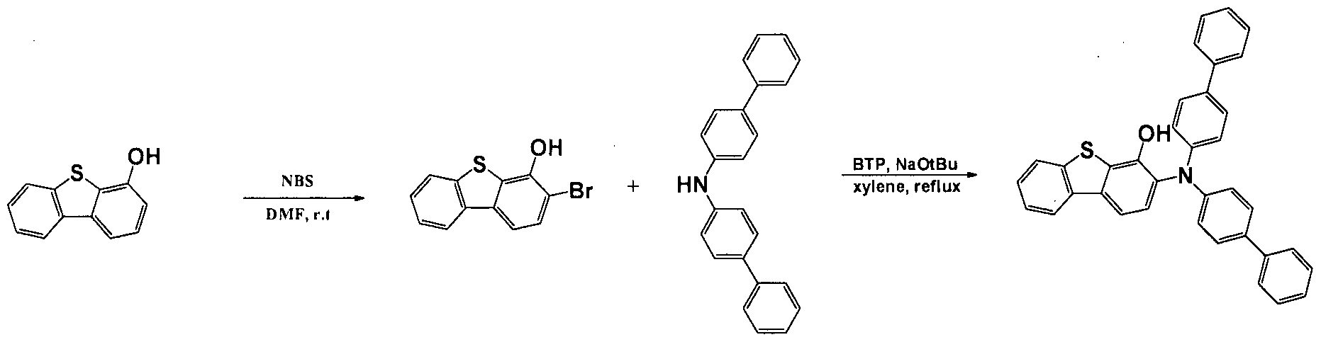
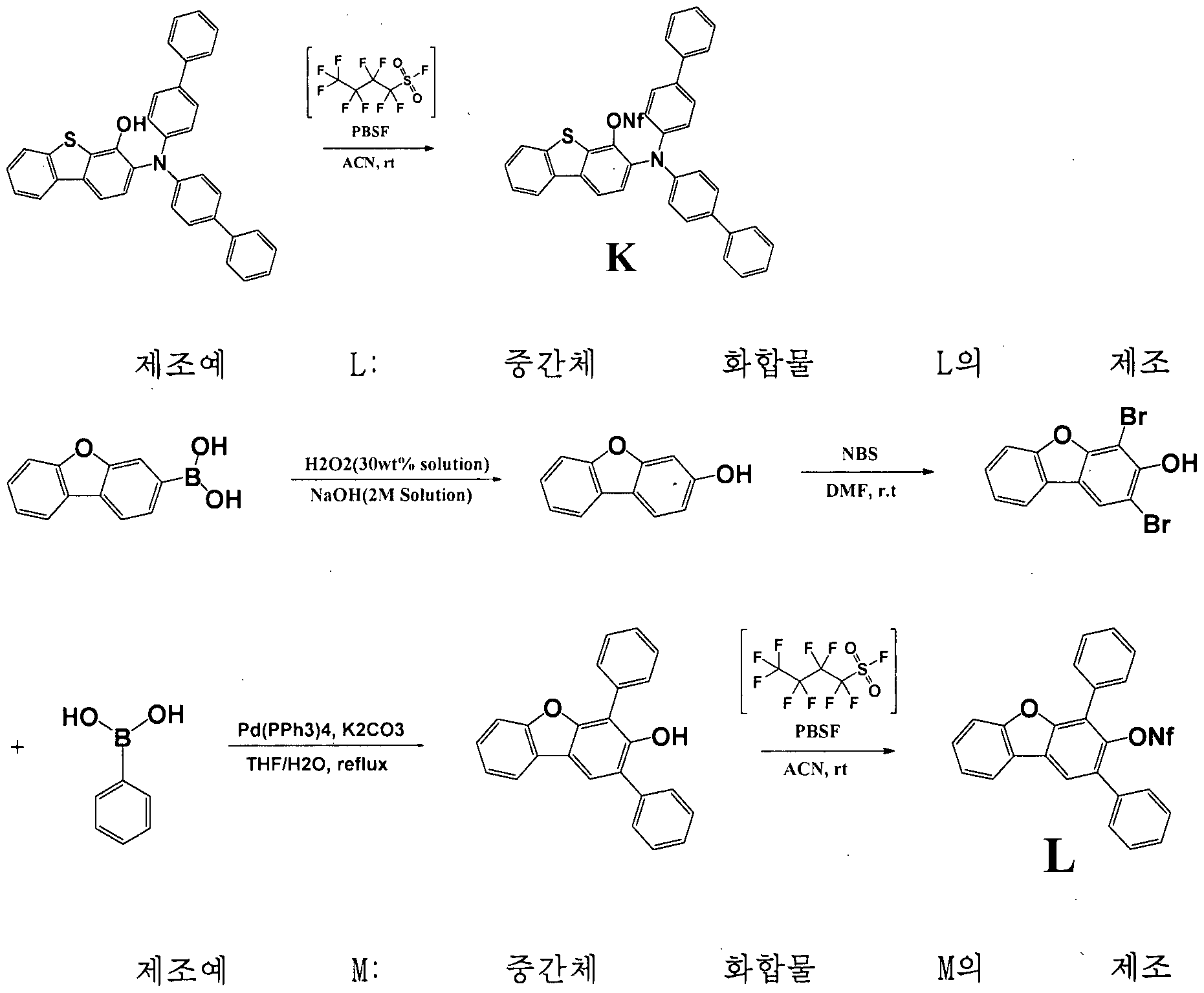
52


MS[M+H]+= 564 제조예 2: 화합물 2의 제조
[화합물 2]

MS[M+H]+= 604 제조예 3: 화합물 3의 제조
[화합물 3]

MS[M+H]+= 694 제조예 4: 화합물 4의 제조

MS[M+H]+= 640 제조예 5: 화합물 5의 제조
[화합물 5]

질소 분위기에서 500ml 등근 바닥 플라스크에 화합물 B(4.96g, 15.55mmol) , N-phenyl-[l , 1 ':4' ,1' '—ter phenyl ]—4— amine (5.49g, 17.10mmol)을 Xylene 260ml에 완전히 녹인 후 Caesium carbonate(6.06g, 18.66薩 ol)을 첨가하고, Bis(tri-ieri-butylphosphine) pal ladium(0)(0.04g, 0.08mmol)을 넣은 후 5 시간 동안 가열 교반하였다. 상온으로 온도를 낮추고 filter하여 base를 제거한 후에 Xylene을 감압농축 시키고 에틸아세테이트 250ml으로 재결정하여 상기 화합물 5(6.08g, 수율: 56%)를 제조하였다.
MS[M+H]+= 640 제조예 6: 화합물 6의 제조
[화합물 6]

MS[M+H]+= 614 제조예 7: 화합물 7의 제조
[화합물 7]

MS[M+H]+= 604 제조예 8: 화합물 8의 제조
[화합물 8]
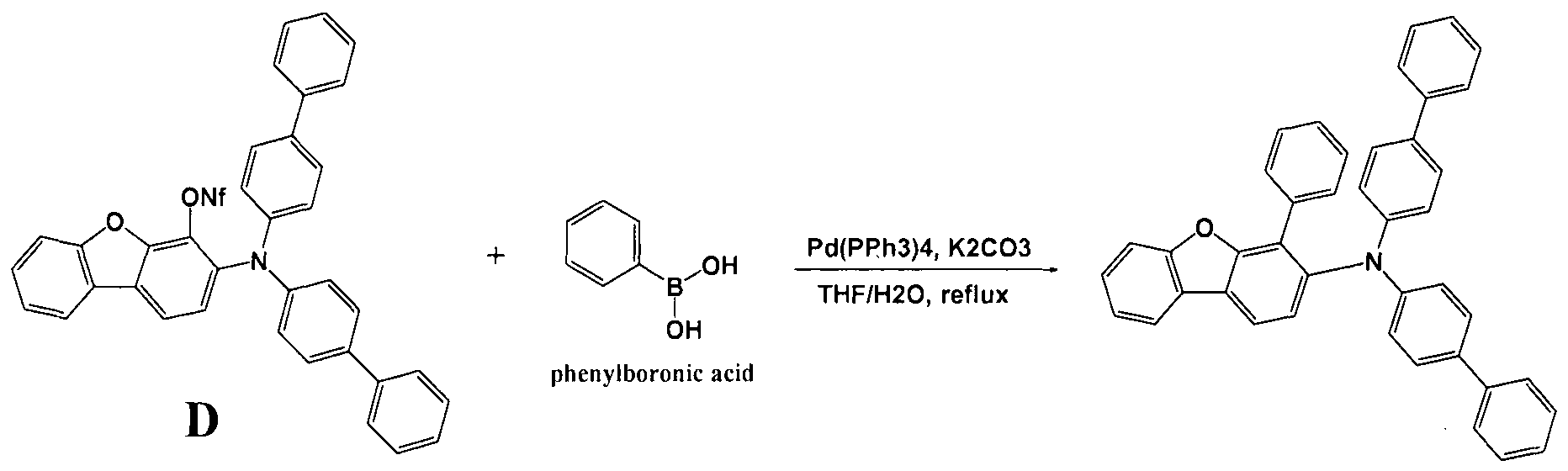
MS[M+H]+= 564 제조예 9: 화합물 9의 제조
[화합물 9]

MS[M+H]+= 614 제조예 10: 화합물 10의 제조

. 질소 분위기에서 500ml 등근 바닥 플라스크에 화합물 E(7.38g, 15.19讓01), phenylboronic aeid(2.13g, 17.46mol)을 테트라하이드로퓨란 240ml에 완전히 녹인 후 2M 탄산칼륨수용액 (120ml )을 첨가하고, 테트라키스- (트리페닐포스핀)팔라듐 (0.49g, 0.46瞧 ol)을 넣은 후 6 시간 동안 가열 교반하였다. 상온으로 온도를 낮추고 물 층을 제거하고 무수황산마그네슴으로 건조한 후 감압농축 시키고 에틸아세테이트 240ml로 재결정하여 상기 화합물 10(8.26g, 수율: 79%)을 제조하였다.
MS[M+H]+= 604 제조예 11: 화합물 11의 제조
[화합물 11]

MS[M+H]+= 654 제조예 12: 화합물 12의 제조

12.90mmol)를 테트라하이드로퓨란 240ml에 완전히 녹인 후 2M
탄산칼륨수용액 (120ml)을 첨가하고, 테트라키스- (트리페닐포스핀)팔라듐 (0.39g, 0.34mmol)을 넣은 후 4 시간 동안 가열 교반하였다. 상온으로 온도를 낮추고 물 층을 제거하고 무수황산마그네슴으로 건조한 후 감압농축 시키고 에틸아세테이트 3K l로 재결정하여 상기 화합물 12(8.2 , 수율: 79%)를 제조하였다.
MS[M+H]+= 786 제조예 13: 화합물 13의 제조

MS[M+H]+= 656 제조예 14: 화합물 14의 제조
[화합물 14]

MS[M+H]+= 580 제조예 15: 화합물 15의 제조

MS[M+H]+= 696 제조예 16: 화합물 16의 제조
[화합물

질소 분위기에서 50( l 등근 바닥 플라스크에 화합물 K(9.68g, 19.28画01), phenyl bor on ic acid(2.61g, 21.40國 ol)을 테트라하이드로퓨란 240ml에 완전히 녹인 후 2M 탄산칼륨수용액 (120ml,)을 첨가하고, 테트라키스- (트리페닐포스핀)팔라듐 (0.67g, 0.58隱 ol)을 넣은 후 .4 시간 동안 가열 교반하였다. 상온으로 온도를 낮추고 물 층을 제거하고 무수황산마그네슘으로 건조한 후 감압농축 시키고 에틸아세테이트 220ml로 재결정하여 상기 화합물 16(6.09g, 수율: 54%)을 제조하였다.
MS[M+H]+= 580 제조예 17: 화합물 17의 제조
[화합물 17]

MS[M+H]+= 640 제조예 18: 화합물 18의 제조

질소 분위기에서 500ml 등근 바닥 플라스크에 화합물 A(6.67g, 27.45隱 01 ) , ( 4- ( [ 1, 1 ' -b i heny 1 ] -4— y 1 (9,9-dimethyl -9H- f 1 uoren-2- yl)amino)phenyl)boronic acid(10.72g, 24.30mol)을 테트라하이드로퓨란 240ml에 완전히 녹인 후 2M 탄산칼륨수용액 (120ml )을 첨가하고, 테트라키스- (트리페닐포스핀)팔라듐 (0.76g, 0.66mmol)을 넣은 후 4 시간 동안 가열
교반하였다. 상온으로 온도를 낮추고 물 층을 제거하고 무수황산마그네슴으로 건조한 후 감압농축 시키고 에틸아세테이트 2.50ml로 재결정하여 상기 화합물 18(7.12g, 수율: 51%)을 제조하였다.
MS[M+H]+= 680 제조예 19: 화합물 19의 제조
[화합물

MS[M+H]+= 690 제조예 20: 화합물 20의 제조
[화합물 20]

MS[M+H]+= 640 제조예 21: 화합물 21의 제조

MS[M+H]+= 696 실시예 1-1
IT0( indium tin oxide)가 Ι,ΟΟΟΑ의 두께로 박막 S팅된 유리 기판을 세제를 녹인 증류수에 넣고. 초음파로 세척하였다. 이 때, 세제로는 피셔사 (Fischer Co.) 제품을 사용하였으며, 증류수로는 밀러포어사 (Mi 11 ipore Co.) 제품의 필터 (Filter)로 2차로 걸러진 증류수를 사용하였다. ITO를 30분간 세척한 후 증류수로 2회 반복하여 초음파 세척을 10분간 진행하였다. 증류수 세척이 끝난 후, 이소프로필알콜, 아세톤, 메탄올의 용제로 초음파 세척을 하고 건조시킨 후 플라즈마 세정기로 수송시켰다. 또한, 산소 플라즈마를 이용하여 상기 기판을 5분간 세정한 후 진공 증착기로 기판을 수송시켰다.
이렇게 준비된 ΠΌ 투명 전극 위에 하기 화학식의 핵사니트릴 핵사아자트리페닐렌 (hexaazatri phenyl ene; HAT)를 150A의 두께로 열 진공 증착하여 정공 주입층을 형성하였다.
[HAT]

상기 정공 주입층 위에 정공을 수송하는 물질인 하기 화합물 HTK1150A)을 진공 증착하여 정공 수송층을 형성하였다.
[HT1]

이어서, 상기 정공 수송층 위에 막 두께 150A으로 상기 제조예 1에서 제조한 화합물 1을 진공 증착하여 전자 차단층을 형성하였다.
이어서, 상기 전자 저지층 위에 막 두께 300A으로 아래와 같은 BH와 BD를 25 : 1의 중량비로 진공증착하여 발광층을 형성하였다.
[BH]


[LiQ]

상기 발광층 위에 상기 화합물 ET과 상기 화합물 LiQ(Li thium Quino l ate)를 1 : 1의 중량비로 진공증착하여 300A의 두께로 전자 수송층을 형성하였다. 상기 전자 수송층 위에 순차적으로 12A두께로 리튬플로라이드 (LiF)와 2 , 000 A 두께로 알루미늄을 증착하여 전자 주입층 및 음극을 형성하였다.
상기의 과정에서 유기물의 증착속도는 0.4~ 0.7A/sec를 유지하였고, 음극의 리튬플로라이드는 으 3A/sec , 알루미늄은 2A/sec의 증착 속도를 유지하였으며, 증착시 진공도는 2 x lO— 7 ~5 x lO"6 torr를 유지하여, 유기 발광 소자를 제작하였다. 실시예 1-2 내지 실시예 1-15
전자 차단층 형성시 화합물 1 대신 하기 표 1과 같이 변경하였다는 점을 제외하고는, 상기 실시예 1-1과 동일한 방법을 이용하여 실시예 1—2 내지 1ᅳ15의 유기 발광 소자를 각각 제작하였다. 비교예 1-1
전자 차단층 형성시 화합물 1 대산 하기 EB— 1을 사용하였다는 점을 제의하고는, 상기 실시예 1-1과 동일한 방법을 이용하여 유기 발광 소자를 제작하였다
[EB-1]

전자 차단층 형성시 화합물 1 대신 하기 EB-2을 사용하였다는 점을 제외하고는, 상기 실시예 1-1과 동일한 방법을 이용하여 유기 발광 소자를 제작하였다
-2]

전자 차단층 형성시 화합물 1 대신 하기 EB-3을 사용하였다는 점을 제외하고는, 상기 실시예 1—1과 동일한 방법을 이용하여 유기 발광 소자를 제작하였다
[EB-3]

전자 차단층 형성시 화합물 1 대신 하기 EB— 4을 사용하였다는 점을 제외하고는, 상기 실시예 1-1과 동일한 방법을 이용하여 유기 발광 소자를 제작하였다
-4]

상기 실시예 1—1 내지 1-15 및 비교예 1ᅳ 1 내지 1-4에서 제작된 유기 발광 소자에 전류를 인가하여, 전압, 효율, 휘도, 색좌표 및 수명을 측정하고 그 결과를 하기 표 1에 나타내었다. T95은 휘도가 초기휘도 (650ni t )에서 95%로 감소되는데 소요되는 시간을 의미한다.
【표 1】
전자 ι2ᄇ 효율 색좌표 수명 차단층
(V@10mA/cm2) (cd/A@10mA/cm2) (x,y) (T95, 화합물 h) 실시예 1- 화합물 1 3.72 5.47 (0.140, 225 1 0.045) 실시예 1ᅳ 화합물 4 3.86 5.32 (0.140, 215 2 0.045) 실시예 1- 화합물 5 3.88 5.31 (0.139, 210 3 0.046) 실시예 1- 화합물 6 3.87 5.38 (0.139, 230 4 0.047) 실시예 1一 화합물 8 3.74 5.41 (0.138, 220 5 0.044) 살시예 1- 화합물 9 3.85 5.28 ' " (0.140, 200 6 0.042) 실시예 1- 화합물 3.81 5.29 (0.140, 205
7 11 0.041)
 비교예 1- EB-2 4.16 4.77 (0.136, 170 2 0.048) 비교예 1- EB-3 4.10 4.82 185 3 비교예 1- EB-4 5.12 4.13 115 4
상기 표 1에서 보는 바와 같이, 본 발명에 따른 화합물을 전자 차단층으로 사용하여 제조된 유기 발광 소자의 경우에 비교예의 유기 발광
S o
소자에 비하여 구동전압, 전류효율, 수명 및 안정성 측면에서!! o o 1 "ᅳᅳ 우수한 성능을 나타냄을 확인할 수 있다. 구체적으로, 본원 발명의 코어와 같은 구조를 가지면서 1번 및 3번 방향에 치환기가 없는 비교예 1-1 내지 1-3의 화합물을 전자억제층으로 사용하여 제조된 유기 발광 소자는, 실시예 대바 효율이 10% 이상, 수명은 30% 이상 떨어지는 결과를 나타내었다.
한편, 비교예 1-4의 화합물은 코어와 아릴아민기 사이의 거리가 너무 멀어서 유기 발광"소자의 특성이 크게 나빠지는 결과를 보였다.
이에, 본원 발명 실시예의 화합물의 경우, 소자의 효율을 높여주는 동시에 안정성이 크게 증가하는 것을 확인할 수 있었다. 실시예 2-1
IT0( indium tin oxide)가 Ι,ΟΟΟΑ의 두께로 박막 코팅된 유리 기판을 세제를 녹인 증류수에 넣고 초음파로 세척하였다. 이 때, 세제로는 피셔사 (Fischer Co.) 제품을 사용하였으몌 증류수로는 밀러포어사 (Mi 11 ipore
Co.) 제품의 필터 (Filter)로 2차로,걸러진 증류수를 사용하였다. IT0를 30분간 세척한 후 증류수로 2회 반복하여 초음파 세척을 10분간 진행하였다. 증류수 세척이 끝난 후, 이소프로필알콜, 아세톤 메탄올의 용제로 초음파 세척을 하고 건조시킨 후 플라즈마 세정기로 수송시켰다. 또한, 산소 플라즈마를 이용하여 상기 기판을 5분간 세정한 후 진공 증착기 S 기판을 수송시켰다.
이렇게 준비된 IT0 투명 전극 위에 상기 HAT를 150 A의 두께로 열 진공 증착하여 정공 주입층을 형성하였다.
상기 정공 주입층 위에 정공을 수송하는 물질로서 상기 제조예 1에서 제조한 화합물 1을 막 두께 1150A으로 진공 증착하여 정공 수송층을 형성하였다.
이어서, 상기 정공 수송층 위에 막 두께 150A으로 하기 화합물 EB를 진공 증착하여 전자 차단층을 형성하였다.

이어서, 상기 전자 저지층 위에 막 두께 300 A으로 상기 BH와 BD를
25:1의 중량비로 진공증착하여 발광층을 형성하였다.
상기 발광층 위에 상기 화합물 ET과 상기 화합물 LiQ Lithium Quinolate)를 1:1의 중량비로 진공증착하여 300A의 두께로 전자 수송층을 형성하였다. 상기 전자 수송층 위에 순차적으로 12A두께로 리튬플로라이드 (LiF)와 2,000A 두께로 알루미늄을 증착하여 전자 주입층 및 음극을 형성하였다.
상기의 과정에서 유기물의 증착속도는 으 4~ 0.7 A/sec를 유지하였고, 음극의 리튬플로라이드는 0.3A/sec, 알루미늄은 2A/sec의 증착 속도를 유지하였으며, 증착시 진공도는 2 χ1(Γ7 ~5 xlO— 6 torr를 유지하여, 유기
발광 소자를 제작하였다. 실시예 2—2 내지 실시예 2-12
정공 수송층 형성시 전자 수송 물질을 화합물 1 대신 하기 표 2와 같이 변경하였다는 점을 제외하고는, 상기 실시예 2-1과 동일한 방법을 이용하여 실시예 2-2 내지 2-12의 유기 발광 소자를 각각 제작하였다. 비교예 2-1
정공 수송층 형성시 전자 수송 물질을 화합물 1 대신 하기 HT-1을 사용하였다는 점을 제외하고는, 상기 실시예 2—1과 동일한 방법을 이용하여 유기 발광 소자를 제작하였다.
-1]

정공 수송층 형성시 전자 수송 물질을 화합물 1 대신 하기 HT-2를 사용하였다는 점을 제외하고는, 상기 실시예 2—1과 동일한 방법을 이용하여 유기 발광 소자를 제작하였다.
[HT-2]
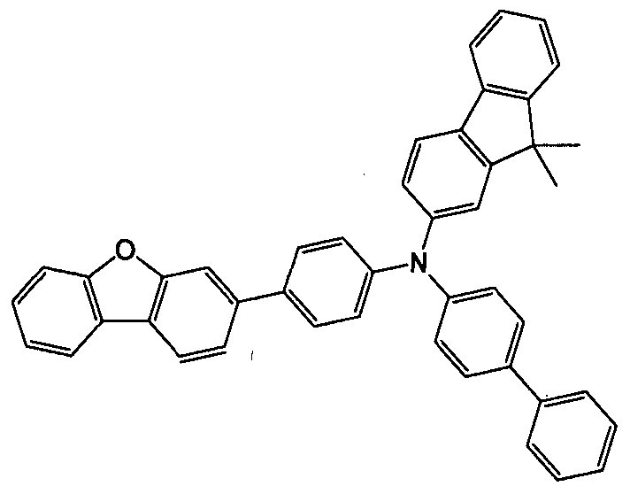
정공 수송층 형성시 전자 수송 물질을 화합물 1 대신 하기 HT-3을 사용하였다는 점을 제외하고는, 상기 실시예 2-1과 동일한 방법을 이용하여 유기 발광 소자를 제작하였다.
-3]

정공 수송층 형성시 전자 수송 물질을 화합물 1 대신 하기 HT-4을 사용하였다는 점을 제외하고는, 상기 실시예 2—1과 동일한 방법을 이용하여 유기 발광 소자를 제작하였다.
[HT-4]

실험예 2
상기 실시예 2-1 내지 2-12 및 비교예 2-1 내지 2-4에서 제작된 유기 발광 소자에 전류를 인가하여, 전압, 효율, 휘도, 색좌표 및 수명을 측정하고 그 결과를 하기 표 2에 나타내었다. T95은 휘도가 초기휘도 (650ni t )에서 95%로 감소되는데 소요되는 시간을 의미한다 .
【표 2]


2 비교예 2- HT-3 4.29 4.87 (0. 136 , 220 3 0.046) 비교예 2- HT-4 4.92 4. 10 110 으
■ 4
상기 표 2에서 보는 바와 같이, 본 발명에 따른 화합물을 정공 수송층으로 사용하여 제조된 유기 .발광 소자의 경우에 비교예의 유기 발광 소자에 비하여 전류효율, 구동전압, 수명 및 안정성 측면에서 우수한 성능을 ^ -나타냄을 확인할 수 있다: ■ ᅳ " ― 구.체적으로, 본원 발명의 코어와 같은 구조를 가지면서 1번 및 3번 방향에 치환기가 없는 비교예 2ᅳ 1 내지 2-3의 화합물을 정공수송층으로 사용하여 제조된 유기 발광 소자는, 실시예 대비 효율이 10% 이상, 수명은 30% 이상 떨어지는 결과를 나타내었다. .
한편, 비교예 2-4의 화합물은 코어와 아릴아민기 사이의 거리가 너무 멀어서 유기 발광'소자의 특성이 크게 나빠지는 결과를 보였다.
이에, 본원 발명 실시예의 화합물의 경우, 소자의 효율을 높여주는 동시에 안정성이 크게 증가하는 것을 확인할 수 있었다. 따라서, 본 발명에 따른 화합물은 전자 차단 능력뿐만 아니라, 정공 수송 능력이 우수하여 유기 발광 소자의 전자차단층 및 /또는 정공수송층에 적용 가능함을 알 수 있다.
【부호의 설명】
1: 기판 2: 양극
3: 발광층 4: 음극
5: 정공주입층 6: 정공수송층
7: 발광층 , 8: 전자수송층
Claims
【청구항. 1】
하기 화학삭 1로 표시되는 화합물:
1]

상기 화학식 1에서,
X는 0또는 S이고,
A 및 B는 각각 독립적으로, 수소; 치환 또는 비치환된 C6-60 아릴; 또는 치환 또는 비치환된 N , 0 및 S로 구성되는 군으로부터 선택되는 헤테로원자를 1개 내지 3개 포함하는 C2-60 헤테로아릴이되, A 및 B가 모두 수소인 경우는 제외하고,
L은 단일 결합; 치환 또는 비치환된 C6-60 아릴렌; 또는 치환 또는 비치환된 0, N , Si 및 S로 구성되는 군으로부터 선택되는 해테로월자를 1개 이상을 포함하는 C2-60 헤테로아릴렌이고,
An 및 Ar2는 각각 독립적으로, 치환 또는 비치환된 C6-60 아릴; 또는 치환 또는 비치환된 N , 0 및 S로 구성되는 군으로부터 선택되는 헤테로원자를 1개 내지 3개 포함하는 C2-60 헤테로아릴이고,
¾은 수소; 중수소; 할로겐; 시아노; 니트로; 아미노; 치환 또는 비치환된 ( 60 알킬; 치환 또는 비치환된 ( 60 할로알킬; 치환 또는 비치환된 d-60 알콕시 ; 치환 또는 비치환된 d-60 할로알콕시 ; 치환 또는 비치환된 C3-60 사이클로알킬; 치환 또는 비치환된 C2-60 알케닐; 치환 또는 비치환된 C6-60 아릴; 치환 '또는 비치환된 C6-60 아릴옥시; 또는 치환 또는 비치환된 N , 0 및 S로 구성되는 군으로부터 선택되는 헤테로원자를 1개 이상 포함하는 C2-60 헤테로고리기이고,
al은 0 내지 4의 정수이다.
【청구항 2]
제 1항에 있어서,
A 및 B는 각각 독립적으로, 하기로 구성되는 군으로부터 선택되는 어느 하나인, 화합물:

상기에서 ,
은 0, S, 또는 CZ4Z5이고,
Ζχ 내지 ζ5는 각각 독립적으로, 수소; 중수소; 할로겐; 시아노; 니트로; 아미노; d-20 알킬; C o 할로알킬; C6-20 아릴; 0 또는 S의 헤테로원자를 1개 이상 포함하는 C2-20 헤테로아릴이고,
nl 내지 n3는 각각 독립적으로, 0 내지 3의 정수이다.
【청구항 3】
제 2항에 있어서,
A 및 B는 각각 독립적으로, 하기로 구성되는 군으로부터 선택되는 어느 하나인 , 화합물:

【청구항 4】
제 1항에 있어서, 하나인,

【청구항 5】
제 4항에 있어서,
L은 단일 결합, 또는 하기로 구성되는 군으로부터 선택되는 어. 하나인, 화합물:

【청구항 6]
제 1항에 있어세
Ar: 및 Ar2는 각각 독립적으로, 하기로 구성되는 군으로부터 선택되 어느 하나인, 화합물:

Y2는 0, S, 또는 cz14z15이고,
Ζπ 내지 Ζ15는 각각 독립적으로, 수소; 중수소; 할로겐; 시아노; 니트로; 아미노; 실릴; d-20 알킬; d_20 할로알킬; C6-2o 아릴; 0 또는 S의 해테로원자를 . 1개 이상 포함하는 C2-20 해테로아릴이되, Z14 및 Z15는 서로 연결되어 단환 또는 다환의 고라를 형성할 수 있고,
ml 내지 m3는 각각 독립적으로, 0 내지 3의 정수이다.
【청구항 7】
제 6항에 있어서
An 및 Ar2는 각각 독립적으로, 하기로 구성되는 군으로부터 선택되는 어느 하나인, 화합물:
98


87


【청구항 8]
제 1항에 있어서,
¾은 수소, 중수소, 할로겐, 시아노, 니트로, 메틸, 또는 페닐 al은 0 또는 1인 , 화합물.
【청구항 9】
제 1항에 있어서,
상기 화합물은 하기 화학식 1A 또는 1B로 표시되는, 화합물: [화학식 1A]


상기 화학식 1A 및 IB 에서 ,
X, A, B, L, An 및 Ar2에 대한 설명은 제 1항에서 정의한 바와 같다.
【청구항 10】
제 1항에 있어서,
상기 화합물은 하기 화합물로 구성되는 군으로부터 선택되는 어 하나인, 화합물:


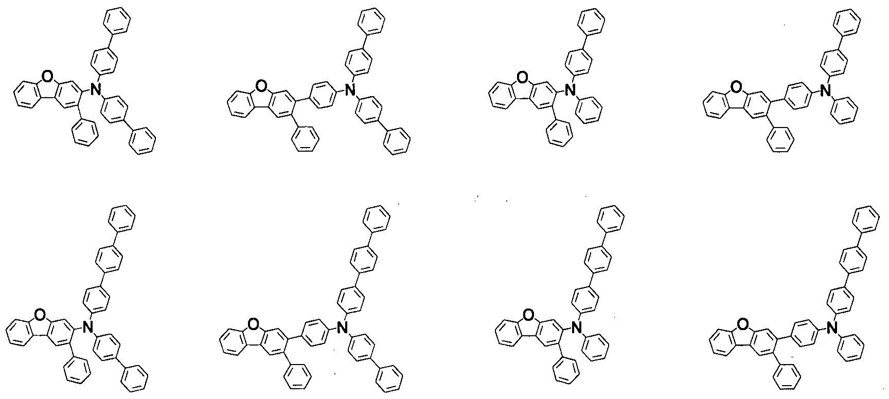
91


92

93

94

95


97


98


99


100


101


102

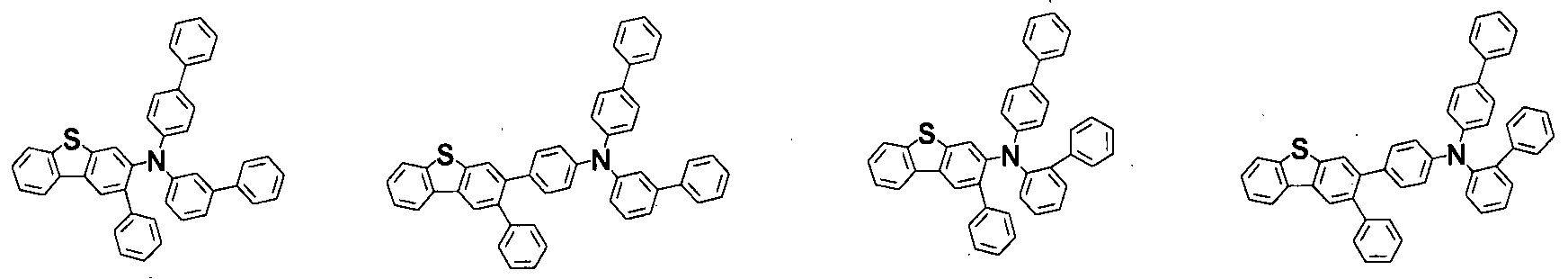

103


104

105

106


109


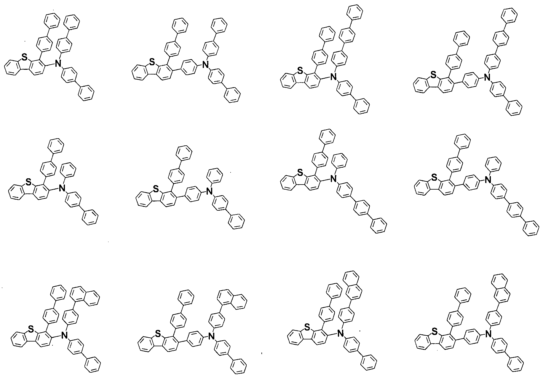


111


 제 1 전극; 상기 제 1 전극과 대향하여 구비된 제 2 전극; 및 상기 저 U 전극과 상기 제 2 전극 사이에 구비된 1층 이상의 유기물층을 포함하는 유기 발광 소자로서, 상기 유기물층 중 1층 이상은 제 1항 내지 제 10항 중 어느 하나의 항에 따른 화합물을 포함하는 것인, 유기 발광 소자.
【청구항 12]
제 11항에 있어서,
상기 화합물을 포함하는 유기물층은 정공주입층; 정공수송층; 또는 정공주입과 정공수송을 동시에 하는 층인, 유기 발광 소자.
【청구항 13】
제 11항에 있어서,
상기 화합물을 포함하는 유기물층은 전자 차단층인, 유기 발광 소자.
Priority Applications (2)
| Application Number | Priority Date | Filing Date | Title |
|---|---|---|---|
| CN201780060444.6A CN109803966B (zh) | 2017-01-26 | 2017-12-21 | 新的基于胺的化合物和使用其的有机发光器件 |
| US16/320,826 US11261176B2 (en) | 2017-01-26 | 2017-12-21 | Amine-based compound and organic light emitting device using the same |
Applications Claiming Priority (4)
| Application Number | Priority Date | Filing Date | Title |
|---|---|---|---|
| KR20170012952 | 2017-01-26 | ||
| KR10-2017-0012952 | 2017-01-26 | ||
| KR1020170149677A KR101967383B1 (ko) | 2017-01-26 | 2017-11-10 | 신규한 아민계 화합물 및 이를 이용한 유기발광 소자 |
| KR10-2017-0149677 | 2017-11-10 |
Publications (2)
| Publication Number | Publication Date |
|---|---|
| WO2018139767A1 WO2018139767A1 (ko) | 2018-08-02 |
| WO2018139767A9 true WO2018139767A9 (ko) | 2019-03-14 |
Family
ID=62978142
Family Applications (1)
| Application Number | Title | Priority Date | Filing Date |
|---|---|---|---|
| PCT/KR2017/015256 WO2018139767A1 (ko) | 2017-01-26 | 2017-12-21 | 신규한 아민계 화합물 및 이를 이용한 유기발광 소자 |
Country Status (2)
| Country | Link |
|---|---|
| US (1) | US11261176B2 (ko) |
| WO (1) | WO2018139767A1 (ko) |
Families Citing this family (3)
| Publication number | Priority date | Publication date | Assignee | Title |
|---|---|---|---|---|
| KR102495414B1 (ko) | 2017-03-08 | 2023-02-02 | 이데미쓰 고산 가부시키가이샤 | 화합물, 유기 전기발광 소자용 재료, 유기 전기발광 소자, 및 전자 기기 |
| KR20220081343A (ko) * | 2019-10-11 | 2022-06-15 | 이데미쓰 고산 가부시키가이샤 | 화합물, 유기 전기발광 소자용 재료, 유기 전기발광 소자 및 전자 기기 |
| KR20210047984A (ko) * | 2019-10-21 | 2021-05-03 | 삼성디스플레이 주식회사 | 발광 소자 및 발광 소자용 아민 화합물 |
Family Cites Families (27)
| Publication number | Priority date | Publication date | Assignee | Title |
|---|---|---|---|---|
| KR100430549B1 (ko) | 1999-01-27 | 2004-05-10 | 주식회사 엘지화학 | 신규한 착물 및 그의 제조 방법과 이를 이용한 유기 발광 소자 및 그의 제조 방법 |
| DE10135513B4 (de) | 2001-07-20 | 2005-02-24 | Novaled Gmbh | Lichtemittierendes Bauelement mit organischen Schichten |
| KR101425423B1 (ko) | 2005-05-30 | 2014-08-01 | 시바 홀딩 인크 | 전계발광 장치 |
| KR101551526B1 (ko) | 2009-08-19 | 2015-09-08 | 이데미쓰 고산 가부시키가이샤 | 방향족 아민 유도체 및 그것을 이용한 유기 전기발광 소자 |
| KR101181261B1 (ko) | 2010-04-21 | 2012-09-10 | 덕산하이메탈(주) | 다이벤조사이오펜과 아릴아민 유도체를 가지는 화합물 및 이를 이용한 유기전기소자, 그 단말 |
| KR101311935B1 (ko) | 2010-04-23 | 2013-09-26 | 제일모직주식회사 | 유기광전소자용 화합물 및 이를 포함하는 유기광전소자 |
| KR20120009761A (ko) | 2010-07-21 | 2012-02-02 | 롬엔드하스전자재료코리아유한회사 | 신규한 유기 발광 화합물 및 이를 포함하는 유기 전계 발광 소자 |
| KR101298483B1 (ko) | 2011-04-01 | 2013-08-21 | 덕산하이메탈(주) | 화합물 및 이를 이용한 유기전기소자, 그 전자장치 |
| JP6128119B2 (ja) * | 2012-05-09 | 2017-05-17 | コニカミノルタ株式会社 | 有機エレクトロルミネッセンス素子、有機エレクトロルミネッセンス素子の製造方法、表示装置および照明装置 |
| JP6278894B2 (ja) | 2012-11-02 | 2018-02-14 | 出光興産株式会社 | 有機エレクトロルミネッセンス素子 |
| US9748492B2 (en) | 2012-11-02 | 2017-08-29 | Idemitsu Kosan Co., Ltd. | Organic electroluminescent device |
| JP2014108938A (ja) | 2012-11-30 | 2014-06-12 | Samsung Display Co Ltd | アリールアミン化合物及びそれを用いた有機電界発光素子 |
| KR20150033082A (ko) | 2013-09-23 | 2015-04-01 | 에스케이케미칼주식회사 | 유기전계발광소자용 화합물 및 이를 포함하는 유기전계발광소자 |
| JP6516407B2 (ja) * | 2013-12-20 | 2019-05-22 | 三星ディスプレイ株式會社Samsung Display Co.,Ltd. | 有機エレクトロルミネッセンス素子用材料及びそれを用いた有機エレクトロルミネッセンス素子 |
| KR102230191B1 (ko) | 2014-05-14 | 2021-03-22 | 삼성디스플레이 주식회사 | 유기 발광 소자 |
| US9732069B2 (en) * | 2014-05-21 | 2017-08-15 | Samsung Electronics Co., Ltd. | Carbazole compound and organic light emitting device including the same |
| KR20160019839A (ko) | 2014-08-11 | 2016-02-22 | 삼성디스플레이 주식회사 | 유기 일렉트로루미네센스 소자용 모노아민 재료 및 이를 사용한 유기 일렉트로루미네센스 소자 |
| KR20160027940A (ko) | 2014-09-02 | 2016-03-10 | 주식회사 엘지화학 | 유기 발광 소자 |
| JP6506534B2 (ja) | 2014-11-07 | 2019-04-24 | 三星ディスプレイ株式會社Samsung Display Co.,Ltd. | 有機電界発光素子用材料及びこれを用いた有機電界発光素子 |
| JP2016100364A (ja) | 2014-11-18 | 2016-05-30 | 三星ディスプレイ株式會社Samsung Display Co.,Ltd. | 有機エレクトロルミネッセンス素子用材料及びそれを用いた有機エレクトロルミネッセンス素子 |
| KR20160060536A (ko) | 2014-11-19 | 2016-05-30 | 삼성디스플레이 주식회사 | 유기 전계 발광 소자 |
| KR101535606B1 (ko) | 2015-01-29 | 2015-07-09 | 덕산네오룩스 주식회사 | 유기전기 소자용 화합물, 이를 이용한 유기전기소자 및 그 전자 장치 |
| KR102559622B1 (ko) | 2015-05-06 | 2023-08-03 | 주식회사 동진쎄미켐 | 신규한 화합물 및 이를 포함하는 유기발광소자 |
| KR101923171B1 (ko) * | 2015-05-27 | 2018-11-28 | 덕산네오룩스 주식회사 | 유기전기 소자용 화합물, 이를 이용한 유기전기소자 및 그 전자 장치 |
| KR102359879B1 (ko) | 2015-06-25 | 2022-02-10 | 덕산네오룩스 주식회사 | 유기전기 소자용 화합물, 이를 이용한 유기전기소자 및 그 전자 장치 |
| CN105503622A (zh) * | 2015-12-14 | 2016-04-20 | 武汉尚赛光电科技有限公司 | 具有电子供体-受体结构的苯并[c]菲类的衍生物、其应用及电致发光器件 |
| KR102521263B1 (ko) | 2016-01-21 | 2023-04-14 | 덕산네오룩스 주식회사 | 유기전기 소자용 화합물, 이를 이용한 유기전기소자 및 그 전자 장치 |
-
2017
- 2017-12-21 US US16/320,826 patent/US11261176B2/en active Active
- 2017-12-21 WO PCT/KR2017/015256 patent/WO2018139767A1/ko active Application Filing
Also Published As
| Publication number | Publication date |
|---|---|
| WO2018139767A1 (ko) | 2018-08-02 |
| US20190169176A1 (en) | 2019-06-06 |
| US11261176B2 (en) | 2022-03-01 |
Similar Documents
| Publication | Publication Date | Title |
|---|---|---|
| KR101885900B1 (ko) | 신규한 헤테로 고리 화합물 및 이를 이용한 유기발광 소자 | |
| KR101953175B1 (ko) | 함질소 다환 화합물 및 이를 이용하는 유기 발광 소자 | |
| JP2018521957A (ja) | ヘテロ環化合物およびこれを含む有機発光素子 | |
| KR101967383B1 (ko) | 신규한 아민계 화합물 및 이를 이용한 유기발광 소자 | |
| JP2020510652A (ja) | 新規な化合物およびこれを用いた有機発光素子 | |
| KR20190098079A (ko) | 헤테로고리 화합물 및 이를 포함하는 유기 발광 소자 | |
| JP2020514335A (ja) | 新規な化合物およびこれを用いた有機発光素子 | |
| JP2019535679A (ja) | 新規なヘテロ環式化合物およびこれを利用した有機発光素子 | |
| JP7124260B2 (ja) | 有機金属化合物およびこれを含む有機発光素子 | |
| WO2019013487A1 (ko) | 신규한 화합물 및 이를 이용한 유기발광 소자 | |
| WO2019017734A1 (ko) | 신규한 헤테로 고리 화합물 및 이를 이용한 유기 발광 소자 | |
| WO2018139767A9 (ko) | 신규한 아민계 화합물 및 이를 이용한 유기발광 소자 | |
| KR101868516B1 (ko) | 신규한 헤테로고리 화합물 및 이를 이용한 유기발광 소자 | |
| WO2019093623A1 (ko) | 신규한 헤테로 고리 화합물 및 이를 이용한 유기발광 소자 | |
| KR20190027708A (ko) | 신규한 페난트렌 화합물 및 이를 이용한 유기발광 소자 | |
| KR102120916B1 (ko) | 유기발광 화합물 및 이를 포함하는 유기전계발광소자 | |
| JP2017521366A (ja) | 複素環化合物及びこれを含む有機発光素子 | |
| CN111225904B (zh) | 杂环化合物及包含其的有机发光装置 | |
| KR20180054502A (ko) | 헤테로고리 화합물 및 이를 포함하는 유기 발광 소자 | |
| JP2019501118A (ja) | 新規な化合物およびこれを含む有機発光素子 | |
| KR20200105388A (ko) | 신규한 화합물 및 이를 이용한 유기발광 소자 | |
| WO2019004612A1 (ko) | 신규한 헤테로 고리 화합물 및 이를 이용한 유기 발광 소자 | |
| KR101757557B1 (ko) | 다환 화합물 및 이를 이용한 유기 전계 발광 소자 | |
| WO2018084426A1 (ko) | 신규한 해테로 고리 화합물 및 이를 이용한 유기발광 소자 | |
| KR101985740B1 (ko) | 헤테로고리 화합물 및 이를 포함하는 유기 발광 소자 |
Legal Events
| Date | Code | Title | Description |
|---|---|---|---|
| 121 | Ep: the epo has been informed by wipo that ep was designated in this application |
Ref document number: 17893783 Country of ref document: EP Kind code of ref document: A1 |
|
| NENP | Non-entry into the national phase |
Ref country code: DE |
|
| 122 | Ep: pct application non-entry in european phase |
Ref document number: 17893783 Country of ref document: EP Kind code of ref document: A1 |