WO2018083990A1 - 撮像素子、撮像装置、並びに電子機器 - Google Patents
撮像素子、撮像装置、並びに電子機器 Download PDFInfo
- Publication number
- WO2018083990A1 WO2018083990A1 PCT/JP2017/037791 JP2017037791W WO2018083990A1 WO 2018083990 A1 WO2018083990 A1 WO 2018083990A1 JP 2017037791 W JP2017037791 W JP 2017037791W WO 2018083990 A1 WO2018083990 A1 WO 2018083990A1
- Authority
- WO
- WIPO (PCT)
- Prior art keywords
- depth
- charge storage
- light shielding
- photodiode
- shielding wall
- Prior art date
- Legal status (The legal status is an assumption and is not a legal conclusion. Google has not performed a legal analysis and makes no representation as to the accuracy of the status listed.)
- Ceased
Links
Images





Classifications
-
- H—ELECTRICITY
- H10—SEMICONDUCTOR DEVICES; ELECTRIC SOLID-STATE DEVICES NOT OTHERWISE PROVIDED FOR
- H10F—INORGANIC SEMICONDUCTOR DEVICES SENSITIVE TO INFRARED RADIATION, LIGHT, ELECTROMAGNETIC RADIATION OF SHORTER WAVELENGTH OR CORPUSCULAR RADIATION
- H10F39/00—Integrated devices, or assemblies of multiple devices, comprising at least one element covered by group H10F30/00, e.g. radiation detectors comprising photodiode arrays
- H10F39/80—Constructional details of image sensors
- H10F39/805—Coatings
- H10F39/8057—Optical shielding
-
- H—ELECTRICITY
- H10—SEMICONDUCTOR DEVICES; ELECTRIC SOLID-STATE DEVICES NOT OTHERWISE PROVIDED FOR
- H10F—INORGANIC SEMICONDUCTOR DEVICES SENSITIVE TO INFRARED RADIATION, LIGHT, ELECTROMAGNETIC RADIATION OF SHORTER WAVELENGTH OR CORPUSCULAR RADIATION
- H10F39/00—Integrated devices, or assemblies of multiple devices, comprising at least one element covered by group H10F30/00, e.g. radiation detectors comprising photodiode arrays
- H10F39/011—Manufacture or treatment of image sensors covered by group H10F39/12
- H10F39/024—Manufacture or treatment of image sensors covered by group H10F39/12 of coatings or optical elements
-
- H—ELECTRICITY
- H10—SEMICONDUCTOR DEVICES; ELECTRIC SOLID-STATE DEVICES NOT OTHERWISE PROVIDED FOR
- H10F—INORGANIC SEMICONDUCTOR DEVICES SENSITIVE TO INFRARED RADIATION, LIGHT, ELECTROMAGNETIC RADIATION OF SHORTER WAVELENGTH OR CORPUSCULAR RADIATION
- H10F39/00—Integrated devices, or assemblies of multiple devices, comprising at least one element covered by group H10F30/00, e.g. radiation detectors comprising photodiode arrays
- H10F39/10—Integrated devices
- H10F39/12—Image sensors
- H10F39/18—Complementary metal-oxide-semiconductor [CMOS] image sensors; Photodiode array image sensors
- H10F39/182—Colour image sensors
-
- H—ELECTRICITY
- H10—SEMICONDUCTOR DEVICES; ELECTRIC SOLID-STATE DEVICES NOT OTHERWISE PROVIDED FOR
- H10F—INORGANIC SEMICONDUCTOR DEVICES SENSITIVE TO INFRARED RADIATION, LIGHT, ELECTROMAGNETIC RADIATION OF SHORTER WAVELENGTH OR CORPUSCULAR RADIATION
- H10F39/00—Integrated devices, or assemblies of multiple devices, comprising at least one element covered by group H10F30/00, e.g. radiation detectors comprising photodiode arrays
- H10F39/80—Constructional details of image sensors
- H10F39/802—Geometry or disposition of elements in pixels, e.g. address-lines or gate electrodes
-
- H—ELECTRICITY
- H10—SEMICONDUCTOR DEVICES; ELECTRIC SOLID-STATE DEVICES NOT OTHERWISE PROVIDED FOR
- H10F—INORGANIC SEMICONDUCTOR DEVICES SENSITIVE TO INFRARED RADIATION, LIGHT, ELECTROMAGNETIC RADIATION OF SHORTER WAVELENGTH OR CORPUSCULAR RADIATION
- H10F39/00—Integrated devices, or assemblies of multiple devices, comprising at least one element covered by group H10F30/00, e.g. radiation detectors comprising photodiode arrays
- H10F39/80—Constructional details of image sensors
- H10F39/807—Pixel isolation structures
-
- H—ELECTRICITY
- H10—SEMICONDUCTOR DEVICES; ELECTRIC SOLID-STATE DEVICES NOT OTHERWISE PROVIDED FOR
- H10P—GENERIC PROCESSES OR APPARATUS FOR THE MANUFACTURE OR TREATMENT OF DEVICES COVERED BY CLASS H10
- H10P50/00—Etching of wafers, substrates or parts of devices
-
- H—ELECTRICITY
- H10—SEMICONDUCTOR DEVICES; ELECTRIC SOLID-STATE DEVICES NOT OTHERWISE PROVIDED FOR
- H10F—INORGANIC SEMICONDUCTOR DEVICES SENSITIVE TO INFRARED RADIATION, LIGHT, ELECTROMAGNETIC RADIATION OF SHORTER WAVELENGTH OR CORPUSCULAR RADIATION
- H10F39/00—Integrated devices, or assemblies of multiple devices, comprising at least one element covered by group H10F30/00, e.g. radiation detectors comprising photodiode arrays
- H10F39/80—Constructional details of image sensors
- H10F39/803—Pixels having integrated switching, control, storage or amplification elements
- H10F39/8037—Pixels having integrated switching, control, storage or amplification elements the integrated elements comprising a transistor
Definitions
- the present disclosure relates to an imaging device, an imaging device, and an electronic device, and in particular, an imaging device and an imaging device that can shield a charge storage unit at low cost while maintaining a charge transfer path from a photodiode to the charge storage unit. And electronic equipment.
- an image pickup element employed in an image pickup apparatus is configured to prevent color mixture between pixels by forming a light blocking structure while holding a charge transfer path from a photodiode to a charge storage unit (patent) Reference 1).
- the present disclosure has been made in view of such a situation, and in particular, allows the charge storage unit to be shielded from light at a low cost while maintaining a charge transfer path from the photodiode to the charge storage unit. .
- An imaging device is arranged in an array, and includes a plurality of photodiodes that generate charges according to the amount of incident light, a charge storage unit that stores charges transferred from the photodiodes, A light-shielding wall that individually shields the photodiode and the charge storage unit, and the light-shielding wall is configured to surround the charge storage unit, a part of which is configured with a first depth, This portion is configured with a second depth, and the first depth and the second depth of the light-shielding wall use a photomask pattern utilizing a processing conversion difference due to a microloading effect.
- This is an image sensor formed by dry etching.
- the light-shielding wall is configured to surround the charge storage unit, and among these, the photodiodes are arrayed for a portion that functions as a charge transfer path for transferring the charge from the photodiode to the charge storage unit.
- the second depth at which the photodiode reaches the substrate layer from the surface on which the photodiodes are arranged in an array is configured with a first depth that does not reach the substrate layer from the surface on which the photodiode is disposed.
- the light shielding wall having the first depth and the second depth is formed by a single dry etching with a single photomask pattern by controlling using a processing conversion difference due to a microloading effect. Can be formed.
- the charge storage unit can be shared by a plurality of photodiodes, and the charge transfer path can be formed between each of the plurality of photodiodes.
- the depth of the groove forming the light shielding wall by the dry etching is controlled by controlling the amount of the reactive gas used in the dry etching to contact the silicon substrate. Can be.
- the photomask pattern is controlled by the dry etching by controlling the contact amount according to the contact area of the reactive gas used for the dry etching with the silicon substrate or the number of flow paths of the reactive gas.
- the depth of the groove forming the light shielding wall can be controlled.
- the contact amount of the reactive gas according to the number of flow paths can be controlled by forming the photomask pattern in an annular structure surrounding the charge storage portion.
- the annular structure can be circular, rhombus, square, or polygon.
- the charge storage unit can include a floating diffusion region and a memory.
- the light shielding wall may be constituted by a transparent insulating film having a refractive index lower than that of silicon or the insulating film having a light shielding metal provided therein.
- An imaging device is arranged in an array and generates a plurality of photodiodes that generate charges according to the amount of incident light; a charge storage unit that stores charges transferred from the photodiodes; A light-shielding wall that individually shields the photodiode and the charge storage unit, and the light-shielding wall is configured to surround the charge storage unit, a part of which is configured with a first depth, This portion is configured with a second depth, and the first depth and the second depth of the light-shielding wall use a photomask pattern utilizing a processing conversion difference due to a microloading effect.
- This is an imaging device formed by dry etching.
- An electronic device is arranged in an array, and generates a plurality of photodiodes that generate charges according to the amount of incident light, a charge storage unit that stores charges transferred from the photodiodes, A light-shielding wall that individually shields the photodiode and the charge storage unit, and the light-shielding wall is configured to surround the charge storage unit, a part of which is configured with a first depth, This portion is configured with a second depth, and the first depth and the second depth of the light-shielding wall use a photomask pattern utilizing a processing conversion difference due to a microloading effect.
- This is an electronic device formed by dry etching.
- the charge accumulation unit that accumulates charges transferred from a plurality of photodiodes that are arranged in an array and generates charges according to the amount of incident light and the photodiodes are individually separated by light shielding walls.
- the light shielding wall is configured to surround the charge storage portion, a part of the light shielding wall is configured with a first depth, and the other part is configured with a second depth,
- the first depth and the second depth of the light shielding wall are formed by dry etching using a photomask pattern using a processing conversion difference due to a microloading effect.
- FIG. 1 is a diagram illustrating a configuration when a unit pixel in a conventional imaging device is viewed from an upper surface (a surface opposite to a light receiving surface).
- the configuration shown in FIG. 1 is a configuration in which two pixels are shared.
- the reset gate is shared by the photodiode 11-1 and the photodiode 11-2 located on the right side of the photodiode 11-1. Yes.
- the unit pixel 1 includes a photodiode 11-1 in the center portion, but when viewed from the top, there is a P region, which is not directly visible, but FIG. 1 shows the positional relationship with other portions. Therefore, the reference numerals are given.
- a floating gate (FG) 15, a floating diffusion region (FD: Floating Diffusion) 14, and a reset gate (RST: Reset Gate) 13 are arranged below the memory unit 16-1.
- the reset gate 13 is shared by the photodiode 11-1 and the photodiode 11-2.
- a transfer gate (TG) 17 is disposed in a part of the photodiode 11-1.
- a wiring 18 is arranged to connect the transfer gate 17 and the memory unit 16-1.
- a memory section 16-2 for the photodiode 11-2 On the right side of the photodiode 11-1, a memory section 16-2 for the photodiode 11-2, a floating gate 21, and a floating diffusion region 20 arranged on the right side of the photodiode 11-1 are provided.
- An amplification transistor (AMP: amplifier) 19 is provided below the floating diffusion region 20.
- the amplification transistor 19 is shared by a plurality of photodiodes. In this case, the amplification transistor 19 is shared by the photodiodes 11-1 and 11-2.
- the transfer gate 17 of the unit pixel 1 having such a configuration is photoelectrically converted by the photodiode 11-1, and the charge accumulated in the photodiode 11-1 is applied to the gate electrode by applying a drive signal.
- the data is transferred to the memory unit 16-1 through the wiring 18.
- the transfer gate 22 is photoelectrically converted by the photodiode 11-2, and the charge accumulated in the photodiode 11-2 is applied to the memory unit 16-2 by applying a drive signal to the gate electrode. Transfer is performed via the wiring 23.
- the memory unit 16-1 is shielded from light by the light shielding film 12-1 and the light shielding film 12-2.
- a light shielding film 12-1 and a light shielding film 12-2 are provided so as to surround the memory portion 16-1. Therefore, the memory unit 16-1 is shielded from light by the light shielding films 12-1 and 12-2.
- the light shielding film 12 is provided in a state of being sandwiched between insulating films.
- the light shielding film 12-2 is provided between the photodiode 11-1 and the memory unit 16-1, the charge from the photodiode 11-1 is transferred through the wiring 18. .
- a part of the insulating film and the light-shielding film 12 may be omitted, and a transfer gate may be provided in that part so that the wiring 18 is not provided.
- the floating gate 15 of the unit pixel 1 transfers the charge accumulated in the memory unit 16-1 to the floating diffusion region 14 by applying a drive signal to the gate electrode of the floating gate 15.
- the floating diffusion region 14 is a charge-voltage conversion unit made of an N-type layer, and converts the charge transferred from the memory unit 16-1 into a voltage under the control of the floating gate 15.
- the unit pixel 1 further includes a reset gate 13 and an amplification transistor 19 shared with the photodiode 11-2.
- the reset gate 13 is connected between the power source and the floating diffusion region 14, and resets the floating diffusion region 14 and the floating diffusion region 20 when a drive signal is applied to the gate electrode.
- the amplification transistor 19 has a drain electrode connected to a power source and a gate electrode connected to the floating diffusion region 14, and reads the voltage of the floating diffusion region 14.
- the unit pixel 1 also includes a selection transistor.
- the selection transistor has a drain electrode connected to a source electrode of the amplification transistor 19 and a source electrode connected to a vertical signal line (not shown). By applying a drive signal to the electrode, the unit pixel 1 from which the pixel signal is to be read out is selected.
- the selection transistor it is possible to adopt a configuration in which the selection transistor is connected between the power source and the drain electrode of the amplification transistor 19.
- the imaging device CMOS image sensor
- starts exposure of all pixels simultaneously ends exposure of all pixels simultaneously, and blocks the charge accumulated in the photodiode 11-1 from the light-shielded memory unit 16
- a global shutter operation global exposure
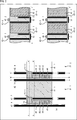
- FIG. 2 is a diagram showing a configuration when a unit pixel from which the wiring 18 is omitted is viewed from the upper surface (surface opposite to the light receiving surface). 2 is a side view of the unit pixel in the left part of FIG.
- the configuration of the unit pixel 31-1 shown in FIG. 2 is basically the same as the configuration of the unit pixel 1 shown in FIG. That is, the unit pixel 31 includes a photodiode 41-1, a transfer gate 47-1, a memory unit 46-1, a floating gate 45-1, a floating diffusion region 44-1, a reset gate 43, and an amplification transistor 48. .
- the unit pixel 31-1 shown in FIG. 2 is also a two-pixel shared type, and the reset gate 43 and the amplification transistor 48 are shared by the photodiode 41-1 and the photodiode 41-2.
- the unit pixel 31 shown in FIG. 2 is compared with the unit pixel 1 shown in FIG.
- the unit pixel 31-1 shown in FIG. 2 also includes the memory unit 46-1, the floating gate 45-1, the floating diffusion region 44-1, and the reset gate 43 in the same manner as the unit pixel 1 shown in FIG. -1 and the light shielding film 42-2.
- the memory unit 46-2, the floating gate 45-2, the floating diffusion region 44-2, and the amplification transistor 48 are disposed between the light shielding film 42-3 and the light shielding film 42-4.
- a part of the light shielding film 42-2 is opened to the photodiode 41-1, and a transfer gate 47-1 is provided in the opened part. Since the transfer gate 47-1 is provided with a part of the light shielding film 42-2 opened, the charge from the photodiode 41-1 is transferred to the memory unit 46-1 without a wiring.
- a part of the light shielding film 42-4 is opened to the photodiode 41-2 side, and the transfer gate 47-2 is formed in the opened part. Is provided. In this way, it is also possible to open a part of the light shielding film and provide a transfer gate in the opened part.
- the right part of FIG. 2 is a side view of the unit pixel 31-1 shown on the left part of FIG. 2 is a diagram when the unit pixel 31-1 shown in the left part of FIG. 2 is viewed from the side when the unit pixel 31-1 is cut along the section aa ′, and the lower right part of FIG. FIG. 6 is a diagram of the unit pixel 31-1 shown on the left side of FIG. 6 when viewed from the side when the bb ′ section is cut.
- the side view shown in the upper right end of FIG. 2 shows a portion where the transfer gate 47-1 is located, and thus the light shielding film 42-2 is provided upward from the lower surface of the unit pixel 31-1.
- the upper surface is not provided but is provided halfway.
- the light shielding film 42-1 is provided so as to penetrate from the lower surface to the upper surface of the unit pixel 31-1 with respect to the light shielding film 42-2.
- the light shielding film 42 in the portion where the transfer gate 47 is provided is provided in the middle of the substrate, and the other light shielding film 42 is provided so as to penetrate the substrate.
- the transfer gate 47 is not located, the light shielding film 42 is provided in a state of penetrating from the lower surface to the upper surface of the substrate.
- the light shielding film 51-1 is provided between the two light shielding films 42, for example, between the light shielding film 42-1 and the light shielding film 42-2, and on the lower surface of the substrate.
- the light shielding film 51 is provided to reduce the influence of unnecessary light from the back side.
- the imaging device according to the present disclosure can form an embedded film that can shield the charge accumulation portion while securing a charge transfer path from the photodiode to the charge accumulation portion with a small photomask pattern, and can reduce the number of processing times. This reduces the increase in manufacturing cost.
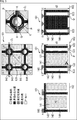
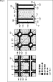
- FIG. 3 shows a configuration example of the imaging device of the present disclosure.
- the upper center of FIG. 3 is a top view as seen from the direction in which light enters the image sensor 101, and the upper right of FIG. 3 is an enlarged view of the range Z1 in the upper center of FIG. 3 is an AB cross section in the upper center part of FIG. 3, the lower central part of FIG. 3 is a CB cross section in the upper center part of FIG. 3, and the lower right part of FIG. 3 is a cross-section taken along the line DE at the upper center of FIG.
- photodiodes (PD) 121 including an N-type layer 141 are arranged in an array with respect to the P-Well 144, and each of them is rectangular.
- a light-shielding film 145 is disposed in the surface layer portion so as to surround the upper surface of the photodiode 121 so as to surround the surface. Further, in the light incident direction (in the upper center of FIG. 3, the direction from the front to the back of the paper, and in the lower part of FIG. 3, the direction from the top to the bottom), the light shielding film 145 is arranged in an array.
- a trench filling film 142 is provided so as to surround each of the arranged photodiodes 121.
- the trench embedding film 142 is made of a transparent insulating film having a refractive index lower than that of silicon, transmits light to the photodiode 121, and is formed in a deep digging DTI (Deep Trench Isolation). In this case, light is shielded up to a critical angle, so that light incident on the adjacent photodiode 121 is shielded and color mixing is suppressed. That is, the trench filling film 142 configured in the DTI substantially functions as a light shielding wall that individually shields the photodiodes 121 and shields the charge storage portions 123 individually.
- DTI Deep Trench Isolation
- the groove filling film 142 is formed linearly with respect to the horizontal direction and the vertical direction of the surface on which the photodiodes 121 are arranged in an array. The part which becomes an intersection is connected so that it may become a circular annular structure. Further, the groove filling film 142 is surrounded by the fixed charge layer 143 formed on the boundary with the P-Well 144. In the following description, the fixed charge layer 143 and the trench filling film 142 will be referred to unless otherwise specified.
- a charge storage portion 123 is formed on the substrate layer 102 which is the central bottom portion of the groove filling film 142 formed in a circular annular structure as viewed from the light incident direction.
- the charge storage unit 123 here is, for example, a floating diffusion region (FD: floating diffusion) (hereinafter also simply referred to as FD) shown in FIG.
- FIG. 4 shows a wiring diagram of a general pixel circuit. 4 includes a photodiode 121, a transfer transistor 122, a charge storage unit 123, a reset transistor 124, an amplification transistor 125, and a selection transistor (SEL) 126.
- SEL selection transistor
- the photodiode 121 accumulates charges according to the amount of incident light.
- the transfer transistor (transfer Tr.) 122 transfers the charge stored in the photodiode 121 to the charge storage unit 123 made of FD (floating diffusion region).
- the reset transistor 124 operates when resetting the charge storage unit 123 or the photodiode 121.
- the amplification transistor 125 is configured such that a voltage corresponding to the charge accumulated in the charge accumulation unit 123 is applied to the gate, and outputs a voltage corresponding to the voltage applied to the gate as a pixel signal.
- the selection transistor 126 opens and closes in response to the selection signal, and is turned on when the selection signal is supplied when the pixel signal is transferred, and the pixel signal output from the amplification transistor 125 is transmitted via the vertical transfer line 127. Output.
- a space having a light shielding property is formed in the groove filling film 142 having a circular annular structure at a portion intersecting with the groove filling film 142 that is linear in the horizontal direction and the vertical direction.
- the charge storage part 123 is formed in a space surrounded by a circular annular structure formed by the groove filling film 142 having the light shielding property, so that the light shielding property is maintained. Further, a part of this circular annular structure groove filling film 142 is shallowly formed so as not to reach the substrate layer 102, and the transfer transistor 122 is formed in this part as shown in the lower center part of FIG. 3. By being formed, a charge transfer path can be secured.
- the groove-filling film 142 is deep only in a portion on the surface where the pixel array is formed and intersecting the groove-filling film 142 formed linearly. The formation is due to the microloading effect.
- a reactive gas including reactive gas (etching gas), ions, radicals, etc.
- etching gas reactive gas
- ions ions
- radicals radicals
- the position P is a position corresponding to the position P shown in the lower center part of FIG. 3, the reactive gas flows from two directions as indicated by an arrow in the upper right column.
- the position Q is a position corresponding to the position Q shown in the lower right part of FIG. 3 and is in three directions as indicated by the arrow in the upper right part of FIG. It has a structure in which reactive gas flows from.
- the groove at the position Q is formed deeper than the position P by the amount of contact of the reactive gas by a larger amount of the reactive gas coming into contact with the position P, thereby forming a deep groove.
- the position P is dug shallower than the position Q by the amount of the reactive gas contact smaller than the position Q, so that the groove is formed shallower.
- the depth d1 of the groove at the position P in the center lower stage in FIG. 3 is shallower than the groove depth d2 (> d1) at the position Q in the lower right stage in FIG.
- the groove depth d2 at the position Q can be configured to reach the substrate layer 102 by adjusting the processing conversion difference, and the groove depth d1 at the position P can be configured not to reach the substrate layer 102. It becomes possible. As a result, it is possible to form the groove filling films 142 having different depths by dry etching using one type of photomask pattern.
- each photomask pattern was required for each depth, but photo processing using processing conversion differences based on the microloading effect was required.
- the mask pattern By using the mask pattern, a plurality of grooves having different depths can be processed by one dry etching even with one photomask pattern.
- the grooves having different depths can be realized by one dry etching using a single photomask pattern. Therefore, as shown in the lower right part of FIG. Can be enclosed by the trench filling film 142, and as shown in the lower middle part of FIG. 3, a transfer transistor 122 is formed in a shallow portion of the trench filling film 142, thereby forming a charge transfer path. Is possible.
- the microloading effect means that the amount of contact of the reactive gas per unit area with respect to the portion etched by the reactive gas at the time of dry etching, that is, the portion dug by contact with the reactive gas. The greater the number, the greater the depth of the effect. Further, hereinafter, the difference generated with respect to the depth of the groove to be dug according to the difference in the contact amount per unit area with the reactive gas by processing using the microloading effect is also referred to as processing conversion difference.
- processing conversion difference is also referred to as processing conversion difference.
- a photomask pattern is formed by photolithography so that the depth of the groove changes depending on the position due to the processing conversion difference based on the microloading effect.
- the photomask pattern to be formed corresponds to the photodiode 121, the transfer transistor 122, and the charge accumulation unit 123 that are formed in advance.
- step S12 a groove whose depth varies depending on the position along the photomask pattern is formed by dry etching using a reactive gas.
- step S13 the fixed charge layer 143 is formed on the entire surface including the dug groove.
- step S14 the groove filling film 142 is buried in the dug groove.
- step S15 a light shielding film 145 is formed.
- membrane 142 from which depth differs by the process conversion difference using a micro loading effect by one dry etching by one photomask pattern was demonstrated, the number of sheets more than that The groove filling film 142 with different depths may be formed by dry etching a plurality of times using the photomask pattern.
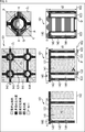
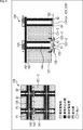
- a metal film having a light shielding property continuing from the light shielding film 145 is buried in the DTI portion of the groove filling film 142.
- the light is reflected into the photodiode 121 by total reflection up to the critical angle between the trench filling film 142 made of an insulating film and silicon, but when the critical angle is exceeded, the light is reflected or absorbed by the metal film forming the light shielding film 145. As a result, color mixing is suppressed.
- the imaging element 101 is connected to the intersection portion of the groove filling film 142 formed linearly with respect to the horizontal direction and the vertical direction of the surface on which the photodiodes 121 are arranged in an array with a circular annular structure.
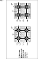
- the shape of the connection at the intersection of the groove filling film 142 may be a shape other than a circle as long as it is an annular structure.
- the intersection portion of the groove embedding film 142 formed linearly with respect to the horizontal direction and the vertical direction of the surface on which the photodiodes 121 are arranged in an array is formed in a diamond shape.
- a structure may be used, or a square structure may be used as shown in the right part of FIG.
- the basic configurations of the AB cross section, the CB cross section, and the DE cross section are the same as those in the lower part of FIG.
- the horizontal width and position in the three types of cross-sectional views in the lower part of FIG. 3 differ depending on the shape.
- the trench embedding film 142 is formed deeply so as to reach the substrate layer 102 so as to shield the charge storage portion 123, and the range in which the transfer transistor 122 is configured can function as a charge transfer path.
- a shallow groove filling film 142 is formed so as not to reach the substrate layer 102.
- the groove for forming the groove embedding film 142 having different depths for forming a transfer transistor serving as a charge transfer path with the photodiode 121 while shielding the charge storage portion 123 is provided as one groove. Since it can be formed by one dry etching using a single photomask pattern, the number of mask patterns and the number of steps can be reduced, and as a result, the manufacturing cost can be reduced.
- the intersection portion of the groove embedding film 142 formed linearly with respect to the horizontal direction and the vertical direction of the surface on which the photodiodes 121 are arranged in an array is formed into an annular structure, so that processing by the microloading effect is performed.
- the reactive gas is changed by changing the width in photolithography for forming the groove for forming the groove filling film 142.
- the depth of the groove to be dug may be adjusted by adjusting the contact amount (contact area) with the groove.
- the groove filling film 142 is formed so as to surround the photodiodes 121 with respect to the surface on which the photodiodes 121 are arranged in an array. Further, the position P and the position Q on the line AB in the left part of FIG. 8 are different in the width of the groove filling film 142 set by the photomask pattern, and the width of the groove filling film 142 centering on the position Q is , The width of the groove filling film 142 centered on the position P is set wider. With such a configuration, the contact amount of the reactive gas at the position Q is larger than the contact amount of the reactive gas at the position P.
- the depth of the groove filling film 142 at the position Q is configured to be deeper than the depth of the groove filling film 142 at the position P, and reaches the substrate layer 102.
- a complete light shielding space of the storage unit 123 is formed.
- the groove buried portion 142 at the position P is shallower than the depth of the groove buried film 142 at the position Q and does not reach the substrate layer 102.
- the transfer transistor 122 is provided to function as a charge transfer path.
- the intersection portion of the groove filling film 142 formed linearly with respect to the horizontal direction and the vertical direction of the surface on which the photodiodes 121 are arranged in an array is formed into an annular structure.
- the depth may be adjusted by changing the width of the groove filling film 142.
- the intersection portion of the groove embedding film 142 formed linearly with respect to the horizontal direction and the vertical direction of the surface on which the photodiodes 121 are arranged in an array has an annular structure.
- the width P of the groove filling film 142 set by the photomask pattern differs between the position P and the position Q on the line AB in the drawing, and the width of the groove filling film 142 centered on the position Q is the position P.
- the width is set wider than the width of the groove filling film 142.
- the depth of the groove filling film 142 at the position Q is configured to be deeper than the depth of the groove filling film 142 at the position P, and reaches the substrate layer 102.
- a complete light shielding space for the charge storage unit 123 is formed.
- the transfer transistor 122 is provided to function as a charge transfer path.
- the left part of FIG. 8 and the central part of FIG. 8 are the number of groove embedding films 142 formed linearly with respect to the horizontal and vertical directions of the surface on which the photodiodes 121 are arranged in an array, and although the crossing points are different configuration examples, the respective AB cross sections are shown in the right part of FIG. In addition, although the AB cross sections of the left part of FIG. 8 and the central part of FIG. 8 are different in width and position in the horizontal direction, the outer shapes are almost the same.
- a single mask pattern is used for the trench embedding film 142 having different depths for forming a transfer transistor serving as a transfer path with the photodiode 121 while shielding the charge storage portion 123 from light. Therefore, the number of mask patterns and the number of processes can be reduced, and as a result, the manufacturing cost can be reduced.
- the width of a part of the groove filling film 142 surrounding each of the photodiodes 121 around the positions P1 and P2 is By forming narrower than the width centered on Q1 and Q2, the amount of contact with the reactive gas during dry etching is reduced, and as shown in the right part of FIG.
- the depth of the trench filling film 142 between the adjacent ⁇ 2 is made shallow so that it does not reach the substrate layer 102.
- a memory that is a charge storage unit 123 and a plurality of photodiodes 121-1, 121-2, etc. are provided on the substrate layer 102 at the bottom of the space between the positions P1 and P2.
- the transfer transistors 122-1 to 122-3 connected to the photodiode 121 it is possible to function as a charge transfer path from the plurality of photodiodes 121.
- the groove filling film 142 at the positions Q1 and Q2 is wider than the groove filling film 142 at the positions P1 and P2, and the contact amount with the reactive gas at the time of dry etching is increased, so that it is dug deeper.
- the structure reaches the substrate layer 102.
- a light-shielding space can be formed between the trench filling films 142, and for example, a pixel transistor such as any of the transistors 124 to 126 can be formed.
- the floating diffusion region (FD: floating diffusion) having different depths, or the groove filling film 142 that shields the charge storage portion 123 constituting the memory and the charge transfer path from the photodiode 121 are made to function.
- One photomask pattern is formed by performing a dry etching process using a photomask pattern in which the width of the groove filling film 142 for forming the transfer transistor is adjusted so as to control the contact amount of the reactive gas.
- the mask pattern for forming the groove burying film 142 that shields the floating diffusion region (FD: floating diffusion) or the charge storage part 123 that constitutes the memory is used as the substrate.
- the contact area is increased or the number of flow paths of the reactive gas is increased so that the contact amount of the reactive gas is increased.
- the mask pattern for forming the trench embedding film 142 for forming the transfer transistor functioning as a charge transfer path from the photodiode 121 is configured so that the deepest portion of the trench embedding film 142 does not reach the substrate layer 102. Since the depth is formed shallower, the contact area of the reactive gas is reduced in order to reduce the contact amount of the reactive gas than the portion where the groove filling film 142 for shielding light is formed, or the number of the reactive gas flow paths is reduced. Reduce.
- a single mask pattern is used as a portion for forming a light shielding space of the charge storage portion 123 and a charge transfer path by one dry etching. It is possible to form the groove embedding film 142 having a depth suitable for each use with the portion where the transfer transistor to be functioned is formed. As a result, the mask pattern can be reduced, and the number of dry etchings, that is, the number of manufacturing steps can be reduced, so that the manufacturing cost can be reduced.
- the above-described imaging device can be applied to various electronic devices such as an imaging device such as a digital still camera or a digital video camera, a mobile phone having an imaging function, or other devices having an imaging function.
- FIG. 10 is a block diagram illustrating a configuration example of an imaging apparatus as an electronic apparatus to which the present technology is applied.
- An imaging apparatus 201 illustrated in FIG. 10 includes an optical system 202, a shutter device 203, a solid-state imaging device 204, a drive circuit 205, a signal processing circuit 206, a monitor 207, and a memory 208, and displays still images and moving images. Imaging is possible.
- the optical system 202 includes one or more lenses, guides light (incident light) from a subject to the solid-state image sensor 204, and forms an image on the light receiving surface of the solid-state image sensor 204.
- the shutter device 203 is disposed between the optical system 202 and the solid-state imaging device 204, and controls the light irradiation period and the light-shielding period to the solid-state imaging device 204 according to the control of the drive circuit 1005.
- the solid-state image sensor 204 is configured by a package including the above-described solid-state image sensor.
- the solid-state imaging device 204 accumulates signal charges for a certain period in accordance with light imaged on the light receiving surface via the optical system 202 and the shutter device 203.
- the signal charge accumulated in the solid-state image sensor 204 is transferred according to a drive signal (timing signal) supplied from the drive circuit 205.
- the drive circuit 205 outputs a drive signal for controlling the transfer operation of the solid-state image sensor 204 and the shutter operation of the shutter device 203 to drive the solid-state image sensor 204 and the shutter device 203.
- the signal processing circuit 206 performs various types of signal processing on the signal charges output from the solid-state imaging device 204.
- An image (image data) obtained by the signal processing by the signal processing circuit 206 is supplied to the monitor 207 and displayed, or supplied to the memory 208 and stored (recorded).
- the imaging device 101 shown in FIG. 3 of the present disclosure is applied in place of the optical system 202, the shutter device 203, and the solid-state imaging device 204 described above, thereby manufacturing the imaging device 201. Cost can be reduced. ⁇ 9. Example of using image sensor >>
- FIG. 11 is a diagram illustrating a usage example in which the image sensor 101 of FIG. 3 described above is used.
- the imaging device described above can be used in various cases for sensing light such as visible light, infrared light, ultraviolet light, and X-rays as follows.
- Devices for taking images for viewing such as digital cameras and mobile devices with camera functions
- Devices used for traffic such as in-vehicle sensors that capture the back, surroundings, and interiors of vehicles, surveillance cameras that monitor traveling vehicles and roads, and ranging sensors that measure distances between vehicles, etc.
- Equipment used for home appliances such as TVs, refrigerators, air conditioners, etc. to take pictures and operate the equipment according to the gestures ⁇ Endoscopes, equipment that performs blood vessel photography by receiving infrared light, etc.
- Equipment used for medical and health care ⁇ Security equipment such as security surveillance cameras and personal authentication cameras ⁇ Skin measuring instrument for photographing skin and scalp photography Such as a microscope to do beauty Equipment used for sports-Equipment used for sports such as action cameras and wearable cameras for sports applications-Used for agriculture such as cameras for monitoring the condition of fields and crops apparatus
- this indication can also take the following structures.
- the light shielding wall is configured to surround the charge storage unit, a part of the light shielding wall is configured with a first depth, and the other part is configured with a second depth,
- the first depth and the second depth are formed by dry etching using a photomask pattern using a processing conversion difference due to a microloading effect.
- the light-shielding wall is configured to surround the charge storage unit.
- a part that functions as a charge transfer path for transferring the charge from the photodiode to the charge storage unit is described with reference to the photodiode.
- the light shielding wall having the first depth and the second depth is controlled once by a single photomask pattern by control using a processing conversion difference due to a microloading effect.
- the imaging device ⁇ 2>, wherein the charge accumulation unit is shared by a plurality of photodiodes, and the charge transfer path is formed between each of the plurality of photodiodes.
- the photomask pattern controls the depth of a groove forming the light-shielding wall by the dry etching by controlling the contact amount of the reactive gas used in the dry etching with the silicon substrate. 1>.
- the photomask pattern is formed by the dry etching by controlling the contact amount according to the contact area of the reactive gas used for the dry etching with the silicon substrate or the number of flow paths of the reactive gas.
- the imaging device according to ⁇ 4>, wherein the depth of the groove forming the light shielding wall is controlled.
- ⁇ 6> The imaging device according to ⁇ 5>, wherein the photomask pattern is formed in an annular structure that surrounds the charge accumulation unit, thereby controlling a contact amount of the reactive gas according to the number of circulation paths.
- the annular structure is a circle, a diamond, a rectangle, or a polygon.
- the charge storage unit includes a floating diffusion region and a memory.
- the light shielding wall includes a transparent insulating film having a refractive index lower than that of silicon, or the insulating film having a light shielding metal provided therein.
- the imaging device according to any one of the above.
- An electronic apparatus in which the first depth and the second depth are formed by dry etching using a photomask pattern using a processing conversion difference due to a microloading effect.
Landscapes
- Solid State Image Pick-Up Elements (AREA)
- Transforming Light Signals Into Electric Signals (AREA)
- Drying Of Semiconductors (AREA)
Abstract
本開示は、フォトダイオードから電荷蓄積部への電荷転送路を保持しつつ、低コストで電荷蓄積部を遮光することができるようにする撮像素子、撮像装置、並びに電子機器に関する。 フォトマスクパターンの形状をのうち、フォトダイオードのそれぞれの混色を防止する遮光性を備えた溝埋め込み膜を形成する溝を形成する部位の反応性ガスが流通する溝の幅や交差数を調整することで反応性ガスとの接触量に応じた溝の深さを調整する。これにより1枚のマスクパターンにより1回のドライエッチングにより複数の深さの溝埋め込み膜を形成することが可能となるので、製造コストを低減させることが可能となる。撮像素子に適用することができる。
Description
本開示は、撮像素子、撮像装置、並びに電子機器に関し、特に、フォトダイオードから電荷蓄積部への電荷転送路を保持しつつ、低コストで電荷蓄積部を遮光できるようにした撮像素子、撮像装置、並びに電子機器に関する。
撮像装置に採用される撮像素子は、一般に、フォトダイオードから電荷蓄積部への電荷転送路を保持しつつ、遮光構造を形成することで、画素間の混色を防止する構成とされている(特許文献1参照)。
しかしながら、上述した特許文献1に記載の技術では、フォトダイオードから電荷蓄積部への電荷転送路を保持しつつ、電荷蓄積部の遮光構造を形成するためには、裏面側からの複数回加工、または両面からの複数回加工が必要である。そのため、エッチングに必要とされるフォトマスクパターンが複数必要となり、工程数も加工回数分増加してしまう。結果として、製造コストを増大させてしまう恐れがあった。
本開示は、このような状況に鑑みてなされたものであり、特に、フォトダイオードから電荷蓄積部への電荷転送路を保持しつつ、低コストで電荷蓄積部を遮光できるようにするものである。
本開示の一側面の撮像素子は、アレイ状に配置され、入射光の光量に応じた電荷を発生する複数のフォトダイオードと、前記フォトダイオードより転送される電荷を蓄積する電荷蓄積部と、前記フォトダイオードおよび前記電荷蓄積部をそれぞれ個別に遮光する遮光壁とを含み、前記遮光壁は、前記電荷蓄積部を取り囲むように構成され、一部の部位が第1の深さで構成され、その他の部位については、第2の深さで構成され、前記遮光壁の前記第1の深さ、および前記第2の深さは、マイクロローディング効果による加工変換差を利用した、フォトマスクパターンを用いたドライエッチングにより形成される撮像素子である。
前記遮光壁は、前記電荷蓄積部を取り囲むように構成され、このうち、前記フォトダイオードから前記電荷蓄積部へと前記電荷を転送する電荷転送路として機能する部位については、前記フォトダイオードがアレイ状に配置された面上から基板層に到達しない第1の深さで構成され、その他の部位については、前記フォトダイオードがアレイ状に配置された面上から基板層に到達する第2の深さで構成され、前記第1の深さ、および前記第2の深さを有する前記遮光壁は、マイクロローディング効果による加工変換差を利用した制御により、1枚のフォトマスクパターンによる1回のドライエッチングにより形成されるようにすることができる。
前記電荷蓄積部は、複数のフォトダイオードにより共有されるようにすることができ、前記複数のフォトダイオードのそれぞれとの間に前記電荷転送路が形成されるようにすることができる。
前記フォトマスクパターンには、前記ドライエッチングにより使用される反応性ガスのシリコン基板への接触量を制御させようにすることで、前記ドライエッチングによる前記遮光壁を形成する溝の深さを制御させるようにすることができる。
前記フォトマスクパターンは、前記ドライエッチングにより使用される反応性ガスのシリコン基板への接触面積、または、前記反応性ガスの流通経路数により接触量を制御させるようにすることで、前記ドライエッチングによる前記遮光壁を形成する溝の深さを制御させるようにすることができる。
前記フォトマスクパターンには、前記電荷蓄積部を取り囲むような環状構造で形成することにより、前記流通経路数による、前記反応性ガスの接触量を制御させるようにすることができる。
前記環状構造は、円形、ひし形、方形、または、多角形とすることができる。
前記電荷蓄積部には、浮遊拡散領域、およびメモリを含ませるようにすることができる。
前記遮光壁は、透過性のある、シリコンよりも屈折率が低い絶縁膜、または、内部に遮光性の金属が設けられた前記絶縁膜より構成されるようにすることができる。
本開示の一側面の撮像装置は、アレイ状に配置され、入射光の光量に応じた電荷を発生する複数のフォトダイオードと、前記フォトダイオードより転送される電荷を蓄積する電荷蓄積部と、前記フォトダイオードおよび前記電荷蓄積部をそれぞれ個別に遮光する遮光壁とを含み、前記遮光壁は、前記電荷蓄積部を取り囲むように構成され、一部の部位が第1の深さで構成され、その他の部位については、第2の深さで構成され、前記遮光壁の前記第1の深さ、および前記第2の深さは、マイクロローディング効果による加工変換差を利用した、フォトマスクパターンを用いたドライエッチングにより形成される撮像装置である。
本開示の一側面の電子機器は、アレイ状に配置され、入射光の光量に応じた電荷を発生する複数のフォトダイオードと、前記フォトダイオードより転送される電荷を蓄積する電荷蓄積部と、前記フォトダイオードおよび前記電荷蓄積部をそれぞれ個別に遮光する遮光壁とを含み、前記遮光壁は、前記電荷蓄積部を取り囲むように構成され、一部の部位が第1の深さで構成され、その他の部位については、第2の深さで構成され、前記遮光壁の前記第1の深さ、および前記第2の深さは、マイクロローディング効果による加工変換差を利用した、フォトマスクパターンを用いたドライエッチングにより形成される電子機器である。
本開示の一側面においては、アレイ状に配置され、入射光の光量に応じた電荷を発生する複数のフォトダイオードより転送される電荷を蓄積する電荷蓄積部および前記フォトダイオードが遮光壁によりそれぞれ個別に遮光され、前記遮光壁は、前記電荷蓄積部を取り囲むように構成され、一部の部位が第1の深さで構成され、その他の部位については、第2の深さで構成され、前記遮光壁の前記第1の深さ、および前記第2の深さは、マイクロローディング効果による加工変換差を利用した、フォトマスクパターンを用いたドライエッチングにより形成される。
本開示の一側面によれば、フォトダイオードから電荷蓄積部への電荷転送路を保持しつつ、低コストで電荷蓄積部を遮光することが可能となる。
以下に添付図面を参照しながら、本開示の好適な実施の形態について詳細に説明する。なお、本明細書及び図面において、実質的に同一の機能構成を有する構成要素については、同一の符号を付することにより重複説明を省略する。
また、以下の順序で説明を行う。
1.従来の撮像素子の概要
2.第1の実施の形態
3.図3の撮像素子の製造処理
4.第1の変形例
5.第2の変形例
6.第3の変形例
7.第4の変形例
8.電子機器への適用例
9.撮像素子の使用例
1.従来の撮像素子の概要
2.第1の実施の形態
3.図3の撮像素子の製造処理
4.第1の変形例
5.第2の変形例
6.第3の変形例
7.第4の変形例
8.電子機器への適用例
9.撮像素子の使用例
<<1.従来の撮像素子の概要>>
本開示の撮像素子を説明するにあたって、従来の撮像素子の概要について説明する。
本開示の撮像素子を説明するにあたって、従来の撮像素子の概要について説明する。
<従来の撮像素子の第1の構成例>
図1は、従来の撮像素子における単位画素を上面(受光面の反対側の面)から見たときの構成を示す図である。図1に示した構成は、2画素共有の構成であり、ここでは、フォトダイオード11-1と、フォトダイオード11-1の右側に位置するフォトダイオード11-2とでリセットゲートなどが共有されている。
図1は、従来の撮像素子における単位画素を上面(受光面の反対側の面)から見たときの構成を示す図である。図1に示した構成は、2画素共有の構成であり、ここでは、フォトダイオード11-1と、フォトダイオード11-1の右側に位置するフォトダイオード11-2とでリセットゲートなどが共有されている。
単位画素1は、中央部分にフォトダイオード11-1を備えるが、上面から見たときにはP領域があるため、直接的には見えないが、図1には、他の部分との位置関係を示すために符号を付している。
メモリ部16-1の下側に並ぶように、フローティングゲート(FG)15、浮遊拡散領域(FD:Floating Diffusion)14、リセットゲート(RST:Reset Gate)13が配置されている。リセットゲート13は、フォトダイオード11-1とフォトダイオード11-2で共有される。
また、フォトダイオード11-1の一部には、転送ゲート(TG:Transfer Gate)17が配置されている。この転送ゲート17とメモリ部16-1とを接続するように配線18が配置されている。フォトダイオード11-1の右側には、フォトダイオード11-1の右側に配置されているフォトダイオード11-2用のメモリ部16-2、フローティングゲート21、浮遊拡散領域20が設けられている。そして、その浮遊拡散領域20の下側に、増幅トランジスタ(AMP:amplifier)19が設けられている。この増幅トランジスタ19は、複数のフォトダイオードと共有され、この場合、フォトダイオード11-1とフォトダイオード11-2で共有される。
このような構成を有する単位画素1の転送ゲート17は、フォトダイオード11-1で光電変換され、フォトダイオード11-1の内部に蓄積された電荷を、ゲート電極に駆動信号が印加されることによってメモリ部16-1に、配線18を介して転送する。同様に、転送ゲート22は、フォトダイオード11-2で光電変換され、フォトダイオード11-2の内部に蓄積された電荷を、ゲート電極に駆動信号が印加されることによってメモリ部16-2に、配線23を介して転送する。
メモリ部16-1は、遮光膜12-1と遮光膜12-2により遮光されている。図1に示したように、メモリ部16-1を囲うように、遮光膜12-1と遮光膜12-2が設けられている。このため、この遮光膜12-1,12-2により、メモリ部16-1は、遮光されている。また、図1に示すように、遮光膜12は、絶縁膜に挟まれた状態で設けられている。
このように、遮光膜12-2が、フォトダイオード11-1とメモリ部16-1との間に設けられているため、フォトダイオード11-1からの電荷は、配線18を介して転送される。なお、詳細は後述するが、絶縁膜と遮光膜12の一部を欠き、その部分に転送ゲートを設ける事で、配線18を設けない構成とすることも可能である。
単位画素1のフローティングゲート15は、メモリ部16-1に蓄積された電荷を、フローティングゲート15のゲート電極に駆動信号が印加されることによって、浮遊拡散領域14に転送する。浮遊拡散領域14は、N型層からなる電荷電圧変換部であり、フローティングゲート15の制御によりメモリ部16-1から転送されてきた電荷を電圧に変換する。
単位画素1はさらに、フォトダイオード11-2と共有されるリセットゲート13と増幅トランジスタ19を有している。リセットゲート13は、電源と浮遊拡散領域14との間に接続されており、ゲート電極に駆動信号が印加されることによって浮遊拡散領域14と浮遊拡散領域20をリセットする。
増幅トランジスタ19は、ドレイン電極が電源に接続され、ゲート電極が浮遊拡散領域14に接続されており、浮遊拡散領域14の電圧を読み出す。図示はしていないが、単位画素1は選択トランジスタも備え、選択トランジスタは、例えば、ドレイン電極が増幅トランジスタ19のソース電極に、ソース電極が図示せぬ垂直信号線にそれぞれ接続されており、ゲート電極に駆動信号が印加されることで、画素信号を読み出すべき単位画素1を選択する。選択トランジスタについては、電源と増幅トランジスタ19のドレイン電極との間に接続した構成を採用することも可能である。
このようにして構成される撮像素子(CMOSイメージセンサ)は、全画素同時に露光を開始し、全画素同時に露光を終了し、フォトダイオード11-1に蓄積された電荷を、遮光されたメモリ部16へ転送することで、グローバルシャッタ動作(グローバル露光)を実現する。このグローバルシャッタ動作により、全画素一致した露光期間による歪みのない撮像が可能となる。
<従来の撮像素子の第2の構成例>
図1の従来の撮像素子においては、転送ゲート17とメモリ部16-1は、配線18を介して接続された例を示したが、配線18は省略するようにしてもよい。図2の左部は、配線18は省略するようにした単位画素を上面(受光面と反対側の面)から見たときの構成を示す図である。また、図2の右上部は、図2の左部の単位画素の側面図である。
図1の従来の撮像素子においては、転送ゲート17とメモリ部16-1は、配線18を介して接続された例を示したが、配線18は省略するようにしてもよい。図2の左部は、配線18は省略するようにした単位画素を上面(受光面と反対側の面)から見たときの構成を示す図である。また、図2の右上部は、図2の左部の単位画素の側面図である。
図2に示した単位画素31-1の構成は、基本的に、図1に示した単位画素1の構成と同様である。すなわち、単位画素31は、フォトダイオード41-1、転送ゲート47-1、メモリ部46-1、フローティングゲート45-1、浮遊拡散領域44-1、リセットゲート43、増幅トランジスタ48から構成されている。
図2に示した単位画素31-1も2画素共有型であり、リセットゲート43と増幅トランジスタ48は、フォトダイオード41-1とフォトダイオード41-2で共有される。図2に示した単位画素31と図1に示した単位画素1とを比較する。
図2に示した単位画素31-1も、図1に示した単位画素1と同じく、メモリ部46-1、フローティングゲート45-1、浮遊拡散領域44-1、リセットゲート43は、遮光膜42-1と遮光膜42-2の間に配置されている。同じく、メモリ部46-2、フローティングゲート45-2、浮遊拡散領域44-2、増幅トランジスタ48は、遮光膜42-3と遮光膜42-4の間に配置されている。
遮光膜42-2の一部は、フォトダイオード41-1側に開口されており、その開口されている部分に転送ゲート47-1が設けられている。転送ゲート47-1が、遮光膜42-2の一部分が開口されて設けられることで、フォトダイオード41-1からの電荷がメモリ部46-1に、配線を介さずに転送される。
他の単位画素、例えば、単位画素31-2も同様に、遮光膜42-4の一部は、フォトダイオード41-2側に開口されており、その開口されている部分に転送ゲート47-2が設けられている。このように、遮光膜の一部分を開口し、その開口された部分に転送ゲートを設けることも可能である。
このように、配線を用いずにフォトダイオード41-1からメモリ部46-1に電荷を転送できるように構成することで、シリコン基板上で電荷の転送ができるようになり、ノイズがのりづらくなり、ノイズにより影響を低減することが可能となる。
図2の右部は、図2の左部に示した単位画素31-1の側面図である。図2の右上段は、図2の左部に示した単位画素31-1をa-a’断面で切断したときの側面から見たときの図であり、図2の右下段は、図2の左部に示した単位画素31-1をb-b’断面で切断したときの側面から見たときの図である。
図2の右上端に示した側面図は、転送ゲート47-1が位置している部分であるため、遮光膜42-2は、単位画素31-1の下面から上方向に設けられているが、上面までは設けられず、途中まで設けられている構成とされる。遮光膜42-2に対して、遮光膜42-1は、単位画素31-1の下面から上面まで貫通した状態で設けられている。このように、転送ゲート47が設けられる部分の遮光膜42は、基板の途中まで設けられている状態にされ、他の遮光膜42は、基板を貫通する状態で設けられる。
図2の右下段に示した側面図は、転送ゲート47が位置していない部分であるため、遮光膜42は、基板の下面から上面に貫通する状態で設けられている。
また、図2の右上段および右下段に示したように、2つの遮光膜42の間、例えば、遮光膜42-1と遮光膜42-2の間であり、基板の下面には、遮光膜51-1が設けられている。この遮光膜51は、裏面側からの不要な光による影響を低減させるために設けられている。
ところが、図1,図2の従来の撮像素子において、フォトダイオードから電荷蓄積部となるメモリ、または浮遊拡散領域(メモリとFGを省略した構成の場合)への電荷転送路を保持したまま、遮光構造を形成するためには、裏面側からの複数回加工、または、表面側および裏面側の両側からの複数回加工が必要となる。このため、フォトマスクパターンが複数必要となり、工程数もフォトマスクパターン数に応じた加工回数分だけ増加してしまう。結果として、製造コストが増大してしまう恐れがあった。
<<2.第1の実施の形態>>
<本開示の撮像素子の構成例>
そこで、本開示の撮像素子は、少ないフォトマスクパターンで、フォトダイオードから電荷蓄積部への電荷転送路を確保しつつ、電荷蓄積部を遮光できるような埋め込み膜を形成できるようにし、加工回数を低減して、製造コストの増大を抑制させるものである。
<本開示の撮像素子の構成例>
そこで、本開示の撮像素子は、少ないフォトマスクパターンで、フォトダイオードから電荷蓄積部への電荷転送路を確保しつつ、電荷蓄積部を遮光できるような埋め込み膜を形成できるようにし、加工回数を低減して、製造コストの増大を抑制させるものである。
図3は、本開示の撮像素子の構成例を示している。図3の中央上段は、撮像素子101における光が入射する方向からみた上面図であり、図3の右上段は、図3の中央上段における範囲Z1の拡大図である。また、図3の左下段は、図3の中央上段におけるA-B断面であり、図3の中央下段は、図3の中央上段におけるC-B断面であり、図3の右下段は、図3の中央上段におけるD-E断面である。
図3の中央上段で示されるように、撮像素子101は、P-Well144に対して、アレイ状にN型層141からなるフォトダイオード(PD)121が配置されており、さらに、それぞれを方形状に囲むように表層部であって、フォトダイオード121の上面を除いた範囲に、遮光膜145が配置されている。また、光の入射方向(図3の中央上段においては、紙面手前から奥手方向、図3の下段においては、上方から下方向を見る方向)からみて、遮光膜145の下には、アレイ状に配置されたフォトダイオード121のそれぞれを取り囲むように、溝埋め込み膜142が設けられている。
溝埋め込み膜142は、透過性のある、シリコンよりも屈折率が低い絶縁膜からなり、フォトダイオード121へと光を透過すると共に、深い掘り込みであるDTI(Deep Trench Isolation)に形成される部位については臨界角までは光を遮光することで、隣接するフォトダイオード121に入射される光を遮光し、混色を抑制するものである。すなわち、DTIに構成された溝埋め込み膜142は、実質的にフォトダイオード121を個別に遮光すると共に、電荷蓄積部123を個別に遮光する遮光壁として機能する。
また、この溝埋め込み膜142は、図3の上段で示されるように、フォトダイオード121がアレイ状に配置された面の、水平方向および垂直方向に対して直線的に形成され、さらに、それぞれの交点となる部位が、円形の環状構造となるように接続されている。さらに、溝埋め込み膜142は、P-Well144との境界に固定電荷層143が成膜されて、全体が取り囲まれている。尚、以降においては、特に断りがない限り、固定電荷層143を含めて、溝埋め込み膜142と称するものとする。
また、光の入射方向からみて円形の環状構造に形成された溝埋め込み膜142の中央底部となる基板層102上には、電荷蓄積部123が形成されている。ここでいう電荷蓄積部123は、例えば、図4で示される浮遊拡散領域(FD:フローティングディフュージョン)(以下、単にFDとも称する)である。
尚、図4は、一般的な画素回路の配線図を示している。図4の画素回路は、フォトダイオード121、転送トランジスタ122、電荷蓄積部123、リセットトランジスタ124、増幅トランジスタ125、および選択トランジスタ(SEL)126より構成される。
フォトダイオード121は、入射光の光量に応じた電荷を蓄積する。転送トランジスタ(転送Tr.)122は、フォトダイオード121に蓄積された電荷をFD(浮遊拡散領域)からなる電荷蓄積部123に転送する。リセットトランジスタ124は、電荷蓄積部123、または、フォトダイオード121をリセットするとき動作する。
増幅トランジスタ125は、ゲートに電荷蓄積部123に蓄積された電荷に応じた電圧が印加される構成とされており、ゲートに印加された電圧に応じた電圧を画素信号として出力する。選択トランジスタ126は、選択信号に応じて開閉し、画素信号を転送する際に選択信号が供給されるときオンにされて、増幅トランジスタ125より出力される画素信号を、垂直転送線127を介して出力する。
水平方向および垂直方向に対して直線状の溝埋め込み膜142と交差する部位における、円形の環状構造からなる溝埋め込み膜142については、遮光性を備えた空間が形成される。電荷蓄積部123は、この遮光性を備えた溝埋め込み膜142によりなる円形の環状構造で取り囲まれた空間内に形成されることで遮光性が保たれる。また、この円形の環状構造の溝埋め込み膜142の一部は、基板層102に到達しないように浅く形成されており、この部位に、図3の中央下段で示されるように、転送トランジスタ122が形成されることにより、電荷の転送経路を確保することが可能となる。
ここで、円形の環状構造の溝埋め込み膜142のうち、画素アレイが形成される面上であって、直線状に形成される溝埋め込み膜142と交差する部位についてのみ、溝埋め込み膜142が深く形成されるのは、マイクロローディング効果によるものである。
すなわち、フォトリソグラフィにより円形の環状構造にエッチングパターンが形成された後、エッチングパターンが形成された表面に対して、反応性ガス(反応性の気体(エッチングガス)やイオン、ラジカル等を含む)が吹き付けられてドライエッチングがなされることにより、溝埋め込み膜142が形成される領域のみが反応することにより、溝が掘り込まれる。その後、掘り込まれた溝の表層に対して、固定電荷層143が形成され、そして、溝を埋めるように溝埋め込み膜142が形成される。
この際、円形の環状構造の溝埋め込み膜142のうち、画素アレイが形成される面上であって、水平方向、および垂直方向に対して直線状に形成される溝埋め込み膜142と交差する部位については、反応性ガスとの反応による掘り込みが進むと、環状構造における部位に応じて、反応性ガスの接触量にばらつきが生じ、掘り込みの深さが変化する。
例えば、図3の右上段の範囲Z1で示されるように、円形の環状構造の溝埋め込み膜142のうち、位置Pは、図3の中央下段で示される位置Pに対応する位置であり、図3の右上段の矢印で示されるように2方向から反応性ガスが流れ込む構造となっている。これに対して、環状構造の溝埋め込み膜142のうち、位置Qは、図3の右下段で示される位置Qに対応する位置であり、図3の右上段の矢印で示されるように3方向から反応性ガスが流れ込む構造となっている。
この結果、位置Qは、位置Pよりも多くの反応性ガスが接触することにより、反応性ガスの接触量が多い分だけ、位置Pより深く掘り込まれることで、溝が深く形成される。逆に、位置Pは、位置Qよりも反応性ガスの接触量が少ない分だけ、位置Qよりも浅く掘り込まれることで、溝が浅く形成される。結果として、図3の中央下段の位置Pの溝の深さd1は、図3の右下段の位置Qにおける溝深さd2(>d1)よりも浅い溝となる。
換言すれば、位置Qは、位置Pよりも多くの方向から反応性ガスが接触することで、反応性ガスとの接触量が増えることにより溝がより深く掘り込まれる(加工変換差が生じる)。したがって、加工変換差を調整することで、位置Qの溝深さd2は基板層102に到達するように構成し、位置Pの溝深さd1を基板層102に到達しないように構成することが可能となる。これにより、1種類のフォトマスクパターンを用いたドライエッチングで、深さの異なる溝埋め込み膜142を形成することが可能となる。
すなわち、これまでは、深さの異なる溝を形成するには、それぞれの深さに対して、それぞれのフォトマスクパターンが必要であったが、マイクロローディング効果に基づいた加工変換差を利用したフォトマスクパターンを用いることで、1枚のフォトマスクパターンでも複数の異なる深さの溝を1回のドライエッチングで加工することが可能となる。
結果として、この深さの異なる溝を1枚のフォトマスクパターンを用いて、1回のドライエッチングにより実現することができるので、図3の右下段で示されるように、電荷蓄積部123の周囲を溝埋め込み膜142により囲い込むことが可能になると共に、図3の中央下段で示されるように、溝埋め込み膜142の浅い部位に転送トランジスタ122を形成することで、電荷転送路を構成することが可能となる。
尚、マイクロローディング効果とは、ドライエッチングの際、反応性ガスによりエッチングされる部位、すなわち、反応性ガスとの接触により掘り込まれる部位に対して、単位面積当たりの反応性ガスの接触量が多いほど、より深く掘り込まれることを表す効果を表すものである。また、以降において、マイクロローディング効果を用いた加工により、反応性ガスとの単位面積当たりの接触量の違いに応じて掘り込まれる溝の深さに対して生じる差を加工変換差とも称する。
<<3.図3の撮像素子の製造処理>>
次に、図5のフローチャートを参照して、図3の撮像素子の製造処理について説明する。尚、事前にフォトダイオード121、転送トランジスタ122、および電荷蓄積部123が形成されていることを前提とする。
<<3.図3の撮像素子の製造処理>>
次に、図5のフローチャートを参照して、図3の撮像素子の製造処理について説明する。尚、事前にフォトダイオード121、転送トランジスタ122、および電荷蓄積部123が形成されていることを前提とする。
ステップS11において、マイクロローディング効果に基づいた加工変換差により溝の深さが位置に応じて変化するようにフォトリソグラフィによりフォトマスクパターンが形成される。ここで、形成されるフォトマスクパターンは、事前に形成されたフォトダイオード121、転送トランジスタ122、および電荷蓄積部123に対応したものとされる。
ステップS12において、反応性ガスを用いたドライエッチングによりフォトマスクパターンに沿って位置に応じて深さが変化する溝が形成される。
すなわち、水平方向および垂直方向に対して直線状の溝埋め込み膜142が形成される領域が交差する部位を、円形の環状構造とすることで、上述した図3の右上段で示される位置P,Qのそれぞれで示されるように深さが異なる溝が形成される。
ステップS13において、掘り込まれた溝を含めた全面に対して固定電荷層143が成膜される。
ステップS14において、掘り込まれた溝に対して溝埋め込み膜142が埋め込まれる。
ステップS15において、遮光膜145が形成される。
以上のような処理により、1枚のフォトマスクパターンによる1回のドライエッチングにより複数の深さの溝埋め込み膜142を形成することが可能となる。
尚、マイクロローディング効果を利用した加工変換差により深さの異なる溝埋め込み膜142を1枚の1枚のフォトマスクパターンによる1回のドライエッチングで実現する例について説明してきたが、それ以上の枚数のフォトマスクパターンを用いて複数回数のドライエッチングにより、深さの異なる溝埋め込み膜142を形成するようにしてもよい。
<<4.第1の変形例>>
以上においては、溝埋め込み膜142は、透過性のある絶縁膜のみから構成される例について説明してきたが、さらに、DTIに遮光膜145の金属膜を埋め込むようにしてもよい。
以上においては、溝埋め込み膜142は、透過性のある絶縁膜のみから構成される例について説明してきたが、さらに、DTIに遮光膜145の金属膜を埋め込むようにしてもよい。
すなわち、図6の下段で示されるように、溝埋め込み膜142におけるDTI部には、遮光膜145から続く遮光性を備えた金属膜が埋め込まれている。絶縁膜からなる溝埋め込み膜142とシリコンの臨界角までは全反射で光がフォトダイオード121内に反射されるが、臨界角を超えると遮光膜145を形成する金属膜によって反射、あるいは吸収されることにより、混色が抑制される。
<<5.第2の変形例>>
以上においては、アレイ状にフォトダイオード121が配列される面の水平方向および垂直方向に対して直線状に形成される溝埋め込み膜142の交点部分を円形の環状構造にして接続する撮像素子101の例について説明してきたが、溝埋め込み膜142の交点部分における接続の形状については、環状構造であれば、円形以外の形状であってもよい。例えば、図7の左部で示されるように、アレイ状にフォトダイオード121が配列される面の水平方向および垂直方向に対して直線状に形成される溝埋め込み膜142の交点部分をひし形の環状構造とするようにしてもよいし、図7の右部で示されるように、方形状の構造としてもよい。
以上においては、アレイ状にフォトダイオード121が配列される面の水平方向および垂直方向に対して直線状に形成される溝埋め込み膜142の交点部分を円形の環状構造にして接続する撮像素子101の例について説明してきたが、溝埋め込み膜142の交点部分における接続の形状については、環状構造であれば、円形以外の形状であってもよい。例えば、図7の左部で示されるように、アレイ状にフォトダイオード121が配列される面の水平方向および垂直方向に対して直線状に形成される溝埋め込み膜142の交点部分をひし形の環状構造とするようにしてもよいし、図7の右部で示されるように、方形状の構造としてもよい。
図7の左部、および図7の右部のいずれにおいても、A-B断面、C-B断面、およびD-E断面の基本構成は図3の下段におけるそれぞれと同様である。ただし、図3の下段における3種類の断面図における水平方向の幅、および位置については、形状の違いに応じて異なるものとなる。
また、環状構造であれば、図7で示されるような形状を含めて円形以外の形状であってもよいが、マイクロローディング効果により生じる加工変換差により、電荷転送路が形成される範囲以外の範囲については、電荷蓄積部123を遮光するように基板層102に到達するように深く溝埋め込み膜142が形成され、転送トランジスタ122が構成される範囲については、電荷転送路として機能できるように、基板層102に到達しない程度に浅い溝埋め込み膜142が形成されるようにする。
いずれの環状構造であっても、電荷蓄積部123を遮光しつつ、フォトダイオード121との電荷転送路となる転送トランジスタを形成するための、深さの異なる溝埋め込み膜142を形成する溝を1枚のフォトマスクパターンを用いて、1回のドライエッチングにより形成することができるので、マスクパターン数、および工程数を低減し、結果として、製造コストを低減することが可能となる。
<<6.第3の変形例>>
以上においては、アレイ状にフォトダイオード121が配列される面の水平方向および垂直方向に対して直線状に形成される溝埋め込み膜142の交点部分を環状構造とすることで、マイクロローディング効果による加工変換差により溝埋め込み膜142の深さを調整する撮像素子101の例について説明してきたが、溝埋め込み膜142を形成するための溝を形成するフォトリソグラフィにおける幅を変化させることで、反応性ガスとの接触量(接触面積)を調整して、掘り込まれる溝の深さを調整するようにしてもよい。
以上においては、アレイ状にフォトダイオード121が配列される面の水平方向および垂直方向に対して直線状に形成される溝埋め込み膜142の交点部分を環状構造とすることで、マイクロローディング効果による加工変換差により溝埋め込み膜142の深さを調整する撮像素子101の例について説明してきたが、溝埋め込み膜142を形成するための溝を形成するフォトリソグラフィにおける幅を変化させることで、反応性ガスとの接触量(接触面積)を調整して、掘り込まれる溝の深さを調整するようにしてもよい。
すなわち、図8の左部で示されるように、溝埋め込み膜142は、アレイ状にフォトダイオード121が配列される面に対して、フォトダイオード121をそれぞれ取り囲むように形成されている。また、図8の左部におけるA-B線上の位置Pと位置Qとは、フォトマスクパターンにより設定される溝埋め込み膜142の幅が異なり、位置Qを中心とする溝埋め込み膜142の幅は、位置Pを中心とする溝埋め込み膜142の幅よりも広く設定されている。このような構成により、位置Qにおける反応性ガスの接触量は、位置Pにおける反応性ガスの接触量よりも多くなる。
このため、図8の右部で示されるように、位置Qにおける溝埋め込み膜142の深さは、位置Pにおける溝埋め込み膜142の深さよりも深い構成とされ基板層102に到達して、電荷蓄積部123の完全な遮光空間を形成する。一方、位置Pにおける溝埋め込み部142は、位置Qにおける溝埋め込み膜142の深さよりも浅くなり、基板層102には到達しない。結果として、位置Pにおいては、基板層102に到達しないので、転送トランジスタ122が設けられることにより電荷転送路として機能する。
また、図8の中央部で示されるように、アレイ状にフォトダイオード121が配列される面の水平方向および垂直方向に対して直線状に形成される溝埋め込み膜142の交点部分を環状構造としたうえで、溝埋め込み膜142の幅に変化を付けて、深さを調整するようにしてもよい。
すなわち、図8の中央部においては、アレイ状にフォトダイオード121が配列される面の水平方向および垂直方向に対して直線状に形成される溝埋め込み膜142の交点部分が環状構造とされているが、図中のA-B上の位置Pと位置Qとでは、フォトマスクパターンにより設定される溝埋め込み膜142の幅が異なり、位置Qを中心とする溝埋め込み膜142の幅は、位置Pの溝埋め込み膜142の幅よりも広く設定されている。このような構成により、位置Qにおける反応性ガスの接触量は、位置Pにおける反応性ガスの接触量よりも多くなる。
このため、図8の右部で示されるように、位置Qにおける溝埋め込み膜142の深さは、位置Pにおける溝埋め込み膜142の深さよりも深く構成とされ、基板層102に到達して、電荷蓄積部123の完全な遮光空間を形成する。一方、位置Pにおける溝埋め込み部142は、位置Qにおける溝埋め込み膜142の深さよりも浅く、基板層102に到達していないため、転送トランジスタ122が設けられることにより電荷転送路として機能する。
すなわち、図8の左部、および図8の中央部は、アレイ状にフォトダイオード121が配列される面の水平方向および垂直方向に対して直線状に形成される溝埋め込み膜142の本数、および、交点部分が異なる構成例であるが、それぞれのA-B断面は、図8の右部で示されるものとなる。尚、図8の左部、および図8の中央部のそれぞれのA-B断面は、詳細には、水平方向の幅や位置が異なるものであるが、外形形状は、ほぼ同様である。
いずれの構造であっても、電荷蓄積部123を遮光しつつ、フォトダイオード121との転送路となる転送トランジスタを形成するための、深さの異なる溝埋め込み膜142を1枚のマスクパターンを用いて、1回のドライエッチングにより形成することができるので、マスクパターン数、および工程数を低減し、結果として、製造コストを低減することが可能となる。
<<7.第4の変形例>>
以上においては、電荷蓄積部123が、1個のフォトダイオード毎に設定される浮遊拡散領域(FD:フローティングディフュージョン)である撮像素子101の例について説明してきたが、電荷蓄積部123を、浮遊拡散領域(FD:フローティングディフュージョン)に代えて、複数のフォトダイオードで共有するメモリにするようにしてもよい。
以上においては、電荷蓄積部123が、1個のフォトダイオード毎に設定される浮遊拡散領域(FD:フローティングディフュージョン)である撮像素子101の例について説明してきたが、電荷蓄積部123を、浮遊拡散領域(FD:フローティングディフュージョン)に代えて、複数のフォトダイオードで共有するメモリにするようにしてもよい。
この場合、例えば、図9の左部のA-B上で示されるように、フォトダイオード121のそれぞれを囲む溝埋め込み膜142のうち、位置P1,P2を中心とする一部の幅を、位置Q1,Q2を中心とする幅よりも狭く形成することで、ドライエッチングの際の反応性ガスとの接触量を低減させ、図7の右部で示されるように、フォトダイオード121-1,121-2とが隣接する間の溝埋め込み膜142の深さを、浅くして、基板層102に到達しない構成とする。
このような構成とすることで、位置P1,P2との間の空間の底部であって基板層102上に、電荷蓄積部123であるメモリとフォトダイオード121-1,121-2等を含む複数のフォトダイオード121とを接続する、転送トランジスタ122-1乃至122-3を設けるようにすることで、複数のフォトダイオード121からの電荷転送路として機能させることができる。
一方、位置Q1,Q2の溝埋め込み膜142は、位置P1,P2における溝埋め込み膜142よりも幅が広く、ドライエッチングの際の反応性ガスとの接触量が多くなるため、より深く掘り込まれることにより、基板層102に到達する構成とする。このような構成とすることで、溝埋め込み膜142間に遮光空間を形成することができ、例えば、トランジスタ124乃至126のいずれかなどの画素トランジスタを形成することができる。
以上の構造によれば、電荷蓄積部123を遮光する基板層102に到達する深さの溝埋め込み膜142と、フォトダイオード121との電荷転送路となる転送トランジスタを形成するための、基板層102に到達しない深さの溝埋め込み膜142とからなる、深さの異なる溝埋め込み膜142を1枚のフォトマスクパターンを用いて、1回のドライエッチングにより形成することが可能となる。これにより、フォトマスクパターン数、および工程数を低減することが可能となるので、結果として、製造コストを低減することが可能となる。
以上をまとめると、それぞれ深さの異なる、浮遊拡散領域(FD:フローティングディフュージョン)、またはメモリを構成する電荷蓄積部123を遮光する溝埋め込み膜142と、フォトダイオード121からの電荷転送路として機能させる転送トランジスタを形成するための溝埋め込み膜142との幅を、反応性ガスの接触量を制御するように調整したフォトマスクパターンを用いて、ドライエッチング処理を施すことにより、1枚のフォトマスクパターンにより1回のドライエッチングで複数の深さの溝埋め込み膜142を形成することが可能となる。結果として、フォトマスクパターン数を低減して、ドライエッチングの工程数を低減させることで、撮像素子の製造コストを低減することが可能となる。
より具体的には、浮遊拡散領域(FD:フローティングディフュージョン)、またはメモリを構成する電荷蓄積部123を遮光する溝埋め込み膜142を形成するためのマスクパターンは、溝埋め込み膜142の最深部を基板層102に到達するように、深さを増大させるため、反応性ガスの接触量が増大するように、接触面積を増大させる、または、反応性ガスの流通経路数を増大させる。
一方、フォトダイオード121からの電荷転送路として機能させる転送トランジスタを形成するための溝埋め込み膜142を形成するためのマスクパターンは、溝埋め込み膜142の最深部が基板層102に到達しないように、深さを浅く形成するので、遮光するための溝埋め込み膜142を形成する部位よりも、反応性ガスの接触量を低減させるため、接触面積を縮小させる、または、反応性ガスの流通経路数を低減させる。
以上のような特徴を備えたマスクパターンを形成することにより、1枚のマスクパターンを用いて、1回のドライエッチングで、電荷蓄積部123の遮光する空間を形成する部位と、電荷転送路として機能させる転送トランジスタを形成する部位とのそれぞれの用途に適切な深さの溝埋め込み膜142を形成することが可能となる。結果として、マスクパターンを低減させることができ、ドライエッチングの回数、すなわち、製造に係る工数を低減させることができるので、製造コストを低減させることが可能となる。
<<8.電子機器への適用例>>
上述した撮像素子は、例えば、デジタルスチルカメラやデジタルビデオカメラなどの撮像装置、撮像機能を備えた携帯電話機、または、撮像機能を備えた他の機器といった各種の電子機器に適用することができる。
上述した撮像素子は、例えば、デジタルスチルカメラやデジタルビデオカメラなどの撮像装置、撮像機能を備えた携帯電話機、または、撮像機能を備えた他の機器といった各種の電子機器に適用することができる。
図10は、本技術を適用した電子機器としての撮像装置の構成例を示すブロック図である。
図10に示される撮像装置201は、光学系202、シャッタ装置203、固体撮像素子204、駆動回路205、信号処理回路206、モニタ207、およびメモリ208を備えて構成され、静止画像および動画像を撮像可能である。
光学系202は、1枚または複数枚のレンズを有して構成され、被写体からの光(入射光)を固体撮像素子204に導き、固体撮像素子204の受光面に結像させる。
シャッタ装置203は、光学系202および固体撮像素子204の間に配置され、駆動回路1005の制御に従って、固体撮像素子204への光照射期間および遮光期間を制御する。
固体撮像素子204は、上述した固体撮像素子を含むパッケージにより構成される。固体撮像素子204は、光学系202およびシャッタ装置203を介して受光面に結像される光に応じて、一定期間、信号電荷を蓄積する。固体撮像素子204に蓄積された信号電荷は、駆動回路205から供給される駆動信号(タイミング信号)に従って転送される。
駆動回路205は、固体撮像素子204の転送動作、および、シャッタ装置203のシャッタ動作を制御する駆動信号を出力して、固体撮像素子204およびシャッタ装置203を駆動する。
信号処理回路206は、固体撮像素子204から出力された信号電荷に対して各種の信号処理を施す。信号処理回路206が信号処理を施すことにより得られた画像(画像データ)は、モニタ207に供給されて表示されたり、メモリ208に供給されて記憶(記録)されたりする。
このように構成されている撮像装置201においても、上述した光学系202、シャッタ装置203、および固体撮像素子204に代えて、本開示の図3で示される撮像素子101を適用することにより、製造コストを低減させることが可能となる。
<<9.撮像素子の使用例>>
<<9.撮像素子の使用例>>
図11は、上述の図3の撮像素子101を使用する使用例を示す図である。
上述した撮像素子は、例えば、以下のように、可視光や、赤外光、紫外光、X線等の光をセンシングする様々なケースに使用することができる。
・ディジタルカメラや、カメラ機能付きの携帯機器等の、鑑賞の用に供される画像を撮影する装置
・自動停止等の安全運転や、運転者の状態の認識等のために、自動車の前方や後方、周囲、車内等を撮影する車載用センサ、走行車両や道路を監視する監視カメラ、車両間等の測距を行う測距センサ等の、交通の用に供される装置
・ユーザのジェスチャを撮影して、そのジェスチャに従った機器操作を行うために、TVや、冷蔵庫、エアーコンディショナ等の家電に供される装置
・内視鏡や、赤外光の受光による血管撮影を行う装置等の、医療やヘルスケアの用に供される装置
・防犯用途の監視カメラや、人物認証用途のカメラ等の、セキュリティの用に供される装置
・肌を撮影する肌測定器や、頭皮を撮影するマイクロスコープ等の、美容の用に供される装置
・スポーツ用途等向けのアクションカメラやウェアラブルカメラ等の、スポーツの用に供される装置
・畑や作物の状態を監視するためのカメラ等の、農業の用に供される装置
・自動停止等の安全運転や、運転者の状態の認識等のために、自動車の前方や後方、周囲、車内等を撮影する車載用センサ、走行車両や道路を監視する監視カメラ、車両間等の測距を行う測距センサ等の、交通の用に供される装置
・ユーザのジェスチャを撮影して、そのジェスチャに従った機器操作を行うために、TVや、冷蔵庫、エアーコンディショナ等の家電に供される装置
・内視鏡や、赤外光の受光による血管撮影を行う装置等の、医療やヘルスケアの用に供される装置
・防犯用途の監視カメラや、人物認証用途のカメラ等の、セキュリティの用に供される装置
・肌を撮影する肌測定器や、頭皮を撮影するマイクロスコープ等の、美容の用に供される装置
・スポーツ用途等向けのアクションカメラやウェアラブルカメラ等の、スポーツの用に供される装置
・畑や作物の状態を監視するためのカメラ等の、農業の用に供される装置
尚、本開示は、以下のような構成も取ることができる。
<1> アレイ状に配置され、入射光の光量に応じた電荷を発生する複数のフォトダイオードと、
前記フォトダイオードより転送される電荷を蓄積する電荷蓄積部と、
前記フォトダイオードおよび前記電荷蓄積部をそれぞれ個別に遮光する遮光壁とを含み、
前記遮光壁は、前記電荷蓄積部を取り囲むように構成され、一部の部位が第1の深さで構成され、その他の部位については、第2の深さで構成され、前記遮光壁の前記第1の深さ、および前記第2の深さは、マイクロローディング効果による加工変換差を利用した、フォトマスクパターンを用いたドライエッチングにより形成される
撮像素子。
<2> 前記遮光壁は、前記電荷蓄積部を取り囲むように構成され、このうち、前記フォトダイオードから前記電荷蓄積部へと前記電荷を転送する電荷転送路として機能する部位については、前記フォトダイオードがアレイ状に配置された面上から基板層に到達しない第1の深さで構成され、その他の部位については、前記フォトダイオードがアレイ状に配置された面上から基板層に到達する第2の深さで構成され、前記第1の深さ、および前記第2の深さを有する前記遮光壁は、マイクロローディング効果による加工変換差を利用した制御により、1枚のフォトマスクパターンによる1回のドライエッチングにより形成される
<1>に記載の撮像素子。
<3> 前記電荷蓄積部は、複数のフォトダイオードにより共有され、前記複数のフォトダイオードのそれぞれとの間に前記電荷転送路が形成される
<2>に記載の撮像素子。
<4> 前記フォトマスクパターンは、前記ドライエッチングにより使用される反応性ガスのシリコン基板への接触量を制御することで、前記ドライエッチングによる前記遮光壁を形成する溝の深さを制御する
<1>に記載の撮像素子。
<5> 前記フォトマスクパターンは、前記ドライエッチングにより使用される反応性ガスのシリコン基板への接触面積、または、前記反応性ガスの流通経路数により接触量を制御することで、前記ドライエッチングによる前記遮光壁を形成する溝の深さを制御する
<4>に記載の撮像素子。
<6> 前記フォトマスクパターンは、前記電荷蓄積部を取り囲むような環状構造で形成することにより、前記流通経路数による、前記反応性ガスの接触量を制御する
<5>に記載の撮像素子。
<7> 前記環状構造は、円形、ひし形、方形、または、多角形である
<6>に記載の撮像素子。
<8> 前記電荷蓄積部は、浮遊拡散領域、およびメモリを含む
<1>乃至<7>のいずれかに記載の撮像素子。
<9> 前記遮光壁は、透過性のある、シリコンよりも屈折率が低い絶縁膜、または、内部に遮光性の金属が設けられた前記絶縁膜より構成される
<1>乃至<8>のいずれかに記載の撮像素子。
<10> アレイ状に配置され、入射光の光量に応じた電荷を発生する複数のフォトダイオードと、
前記フォトダイオードより転送される電荷を蓄積する電荷蓄積部と、
前記フォトダイオードおよび前記電荷蓄積部をそれぞれ個別に遮光する遮光壁とを含み、
前記遮光壁は、前記電荷蓄積部を取り囲むように構成され、一部の部位が第1の深さで構成され、その他の部位については、第2の深さで構成され、前記遮光壁の前記第1の深さ、および前記第2の深さは、マイクロローディング効果による加工変換差を利用した、フォトマスクパターンを用いたドライエッチングにより形成される
撮像装置。
<11> アレイ状に配置され、入射光の光量に応じた電荷を発生する複数のフォトダイオードと、
前記フォトダイオードより転送される電荷を蓄積する電荷蓄積部と、
前記フォトダイオードおよび前記電荷蓄積部をそれぞれ個別に遮光する遮光壁とを含み、
前記遮光壁は、前記電荷蓄積部を取り囲むように構成され、一部の部位が第1の深さで構成され、その他の部位については、第2の深さで構成され、前記遮光壁の前記第1の深さ、および前記第2の深さは、マイクロローディング効果による加工変換差を利用した、フォトマスクパターンを用いたドライエッチングにより形成される
電子機器。
<1> アレイ状に配置され、入射光の光量に応じた電荷を発生する複数のフォトダイオードと、
前記フォトダイオードより転送される電荷を蓄積する電荷蓄積部と、
前記フォトダイオードおよび前記電荷蓄積部をそれぞれ個別に遮光する遮光壁とを含み、
前記遮光壁は、前記電荷蓄積部を取り囲むように構成され、一部の部位が第1の深さで構成され、その他の部位については、第2の深さで構成され、前記遮光壁の前記第1の深さ、および前記第2の深さは、マイクロローディング効果による加工変換差を利用した、フォトマスクパターンを用いたドライエッチングにより形成される
撮像素子。
<2> 前記遮光壁は、前記電荷蓄積部を取り囲むように構成され、このうち、前記フォトダイオードから前記電荷蓄積部へと前記電荷を転送する電荷転送路として機能する部位については、前記フォトダイオードがアレイ状に配置された面上から基板層に到達しない第1の深さで構成され、その他の部位については、前記フォトダイオードがアレイ状に配置された面上から基板層に到達する第2の深さで構成され、前記第1の深さ、および前記第2の深さを有する前記遮光壁は、マイクロローディング効果による加工変換差を利用した制御により、1枚のフォトマスクパターンによる1回のドライエッチングにより形成される
<1>に記載の撮像素子。
<3> 前記電荷蓄積部は、複数のフォトダイオードにより共有され、前記複数のフォトダイオードのそれぞれとの間に前記電荷転送路が形成される
<2>に記載の撮像素子。
<4> 前記フォトマスクパターンは、前記ドライエッチングにより使用される反応性ガスのシリコン基板への接触量を制御することで、前記ドライエッチングによる前記遮光壁を形成する溝の深さを制御する
<1>に記載の撮像素子。
<5> 前記フォトマスクパターンは、前記ドライエッチングにより使用される反応性ガスのシリコン基板への接触面積、または、前記反応性ガスの流通経路数により接触量を制御することで、前記ドライエッチングによる前記遮光壁を形成する溝の深さを制御する
<4>に記載の撮像素子。
<6> 前記フォトマスクパターンは、前記電荷蓄積部を取り囲むような環状構造で形成することにより、前記流通経路数による、前記反応性ガスの接触量を制御する
<5>に記載の撮像素子。
<7> 前記環状構造は、円形、ひし形、方形、または、多角形である
<6>に記載の撮像素子。
<8> 前記電荷蓄積部は、浮遊拡散領域、およびメモリを含む
<1>乃至<7>のいずれかに記載の撮像素子。
<9> 前記遮光壁は、透過性のある、シリコンよりも屈折率が低い絶縁膜、または、内部に遮光性の金属が設けられた前記絶縁膜より構成される
<1>乃至<8>のいずれかに記載の撮像素子。
<10> アレイ状に配置され、入射光の光量に応じた電荷を発生する複数のフォトダイオードと、
前記フォトダイオードより転送される電荷を蓄積する電荷蓄積部と、
前記フォトダイオードおよび前記電荷蓄積部をそれぞれ個別に遮光する遮光壁とを含み、
前記遮光壁は、前記電荷蓄積部を取り囲むように構成され、一部の部位が第1の深さで構成され、その他の部位については、第2の深さで構成され、前記遮光壁の前記第1の深さ、および前記第2の深さは、マイクロローディング効果による加工変換差を利用した、フォトマスクパターンを用いたドライエッチングにより形成される
撮像装置。
<11> アレイ状に配置され、入射光の光量に応じた電荷を発生する複数のフォトダイオードと、
前記フォトダイオードより転送される電荷を蓄積する電荷蓄積部と、
前記フォトダイオードおよび前記電荷蓄積部をそれぞれ個別に遮光する遮光壁とを含み、
前記遮光壁は、前記電荷蓄積部を取り囲むように構成され、一部の部位が第1の深さで構成され、その他の部位については、第2の深さで構成され、前記遮光壁の前記第1の深さ、および前記第2の深さは、マイクロローディング効果による加工変換差を利用した、フォトマスクパターンを用いたドライエッチングにより形成される
電子機器。
101 撮像素子, 102 基板層, 121 フォトダイオード, 122 転送トランジスタ, 123 電荷蓄積部, 124 リセットトランジスタ, 125 増幅トランジスタ, 126 選択トランジスタ, 127 垂直転送線, 141 N型層, 142 溝埋め込み層, 143 固定電荷層, 144 P-Well, 145 遮光膜
Claims (11)
- アレイ状に配置され、入射光の光量に応じた電荷を発生する複数のフォトダイオードと、
前記フォトダイオードより転送される電荷を蓄積する電荷蓄積部と、
前記フォトダイオードおよび前記電荷蓄積部をそれぞれ個別に遮光する遮光壁とを含み、
前記遮光壁は、前記電荷蓄積部を取り囲むように構成され、一部の部位が第1の深さで構成され、その他の部位については、第2の深さで構成され、前記遮光壁の前記第1の深さ、および前記第2の深さは、マイクロローディング効果による加工変換差を利用した、フォトマスクパターンを用いたドライエッチングにより形成される
撮像素子。 - 前記遮光壁は、前記電荷蓄積部を取り囲むように構成され、このうち、前記フォトダイオードから前記電荷蓄積部へと前記電荷を転送する電荷転送路として機能する部位については、前記フォトダイオードがアレイ状に配置された面上から基板層に到達しない第1の深さで構成され、その他の部位については、前記フォトダイオードがアレイ状に配置された面上から基板層に到達する第2の深さで構成され、前記第1の深さ、および前記第2の深さを有する前記遮光壁は、マイクロローディング効果による加工変換差を利用した制御により、1枚のフォトマスクパターンによる1回のドライエッチングにより形成される
請求項1に記載の撮像素子。 - 前記電荷蓄積部は、複数のフォトダイオードにより共有され、前記複数のフォトダイオードのそれぞれとの間に前記電荷転送路が形成される
請求項2に記載の撮像素子。 - 前記フォトマスクパターンは、前記ドライエッチングにより使用される反応性ガスのシリコン基板への接触量を制御することで、前記ドライエッチングによる前記遮光壁を形成する溝の深さを制御する
請求項1に記載の撮像素子。 - 前記フォトマスクパターンは、前記ドライエッチングにより使用される反応性ガスのシリコン基板への接触面積、または、前記反応性ガスの流通経路数により接触量を制御することで、前記ドライエッチングによる前記遮光壁を形成する溝の深さを制御する
請求項4に記載の撮像素子。 - 前記フォトマスクパターンは、前記電荷蓄積部を取り囲むような環状構造で形成することにより、前記流通経路数による、前記反応性ガスの接触量を制御する
請求項5に記載の撮像素子。 - 前記環状構造は、円形、ひし形、方形、または、多角形である
請求項6に記載の撮像素子。 - 前記電荷蓄積部は、浮遊拡散領域、およびメモリを含む
請求項1に記載の撮像素子。 - 前記遮光壁は、透過性のある、シリコンよりも屈折率が低い絶縁膜、または、内部に遮光性の金属が設けられた前記絶縁膜より構成される
請求項1に記載の撮像素子。 - アレイ状に配置され、入射光の光量に応じた電荷を発生する複数のフォトダイオードと、
前記フォトダイオードより転送される電荷を蓄積する電荷蓄積部と、
前記フォトダイオードおよび前記電荷蓄積部をそれぞれ個別に遮光する遮光壁とを含み、
前記遮光壁は、前記電荷蓄積部を取り囲むように構成され、一部の部位が第1の深さで構成され、その他の部位については、第2の深さで構成され、前記遮光壁の前記第1の深さ、および前記第2の深さは、マイクロローディング効果による加工変換差を利用した、フォトマスクパターンを用いたドライエッチングにより形成される
撮像装置。 - アレイ状に配置され、入射光の光量に応じた電荷を発生する複数のフォトダイオードと、
前記フォトダイオードより転送される電荷を蓄積する電荷蓄積部と、
前記フォトダイオードおよび前記電荷蓄積部をそれぞれ個別に遮光する遮光壁とを含み、
前記遮光壁は、前記電荷蓄積部を取り囲むように構成され、一部の部位が第1の深さで構成され、その他の部位については、第2の深さで構成され、前記遮光壁の前記第1の深さ、および前記第2の深さは、マイクロローディング効果による加工変換差を利用した、フォトマスクパターンを用いたドライエッチングにより形成される
電子機器。
Priority Applications (5)
| Application Number | Priority Date | Filing Date | Title |
|---|---|---|---|
| JP2018548620A JPWO2018083990A1 (ja) | 2016-11-02 | 2017-10-19 | 撮像素子、撮像装置、並びに電子機器 |
| CN201780063262.4A CN109863600B (zh) | 2016-11-02 | 2017-10-19 | 成像器件、成像装置以及电子设备 |
| US16/343,529 US11037972B2 (en) | 2016-11-02 | 2017-10-19 | Imaging device, imaging apparatus, and electronic device |
| US17/314,159 US20210265405A1 (en) | 2016-11-02 | 2021-05-07 | Imaging device, imaging apparatus, and electronic device |
| JP2022141507A JP2022168045A (ja) | 2016-11-02 | 2022-09-06 | 撮像素子、撮像装置、並びに電子機器 |
Applications Claiming Priority (2)
| Application Number | Priority Date | Filing Date | Title |
|---|---|---|---|
| JP2016-215045 | 2016-11-02 | ||
| JP2016215045 | 2016-11-02 |
Related Child Applications (2)
| Application Number | Title | Priority Date | Filing Date |
|---|---|---|---|
| US16/343,529 A-371-Of-International US11037972B2 (en) | 2016-11-02 | 2017-10-19 | Imaging device, imaging apparatus, and electronic device |
| US17/314,159 Continuation US20210265405A1 (en) | 2016-11-02 | 2021-05-07 | Imaging device, imaging apparatus, and electronic device |
Publications (1)
| Publication Number | Publication Date |
|---|---|
| WO2018083990A1 true WO2018083990A1 (ja) | 2018-05-11 |
Family
ID=62076778
Family Applications (1)
| Application Number | Title | Priority Date | Filing Date |
|---|---|---|---|
| PCT/JP2017/037791 Ceased WO2018083990A1 (ja) | 2016-11-02 | 2017-10-19 | 撮像素子、撮像装置、並びに電子機器 |
Country Status (4)
| Country | Link |
|---|---|
| US (2) | US11037972B2 (ja) |
| JP (2) | JPWO2018083990A1 (ja) |
| CN (1) | CN109863600B (ja) |
| WO (1) | WO2018083990A1 (ja) |
Cited By (5)
| Publication number | Priority date | Publication date | Assignee | Title |
|---|---|---|---|---|
| CN112292760A (zh) * | 2018-06-21 | 2021-01-29 | 索泰克公司 | 前侧型图像传感器和制造这种传感器的方法 |
| JPWO2021131318A1 (ja) * | 2019-12-24 | 2021-07-01 | ||
| WO2021153030A1 (ja) * | 2020-01-29 | 2021-08-05 | ソニーセミコンダクタソリューションズ株式会社 | 固体撮像装置およびその製造方法 |
| WO2021172036A1 (ja) * | 2020-02-28 | 2021-09-02 | ソニーセミコンダクタソリューションズ株式会社 | センサ素子およびセンサ装置 |
| TWI844550B (zh) * | 2018-12-03 | 2024-06-11 | 日商索尼半導體解決方案公司 | 成像裝置 |
Families Citing this family (6)
| Publication number | Priority date | Publication date | Assignee | Title |
|---|---|---|---|---|
| TWI865651B (zh) | 2019-11-18 | 2024-12-11 | 日商索尼半導體解決方案公司 | 固體攝像裝置及電子機器 |
| JP2023023218A (ja) | 2021-08-04 | 2023-02-16 | キヤノン株式会社 | 光電変換装置 |
| KR20230093563A (ko) | 2021-12-20 | 2023-06-27 | 삼성전자주식회사 | 이미지 센서 및 이의 제조 방법 |
| CN115663002A (zh) * | 2022-11-03 | 2023-01-31 | 豪威科技(上海)有限公司 | 图像传感器的制作方法 |
| CN118073377B (zh) * | 2022-11-23 | 2024-11-12 | 武汉新芯集成电路股份有限公司 | 垂直电荷转移成像传感器及其制作方法 |
| CN118293799B (zh) * | 2024-04-12 | 2024-09-20 | 苏州朗伯威智能科技有限公司 | 一种相移结构光三维成像方法和系统 |
Citations (7)
| Publication number | Priority date | Publication date | Assignee | Title |
|---|---|---|---|---|
| JP2006032549A (ja) * | 2004-07-14 | 2006-02-02 | Toshiba Corp | 半導体装置および半導体装置の製造方法 |
| JP2013065688A (ja) * | 2011-09-16 | 2013-04-11 | Sony Corp | 固体撮像素子および製造方法、並びに電子機器 |
| JP2014096490A (ja) * | 2012-11-09 | 2014-05-22 | Sony Corp | 撮像素子、製造方法 |
| US20140327051A1 (en) * | 2013-05-02 | 2014-11-06 | Samsung Electronics Co., Ltd. | Image sensor and method of manufacturing the same |
| JP2015023259A (ja) * | 2013-07-23 | 2015-02-02 | 株式会社東芝 | 固体撮像装置およびその製造方法 |
| JP2015053411A (ja) * | 2013-09-09 | 2015-03-19 | ソニー株式会社 | 固体撮像素子、固体撮像素子の製造方法、および電子機器 |
| WO2016143531A1 (ja) * | 2015-03-09 | 2016-09-15 | ソニー株式会社 | 撮像素子及びその製造方法、並びに電子機器 |
Family Cites Families (9)
| Publication number | Priority date | Publication date | Assignee | Title |
|---|---|---|---|---|
| JP4075797B2 (ja) * | 2003-12-25 | 2008-04-16 | ソニー株式会社 | 固体撮像素子 |
| US20100269084A1 (en) * | 2008-11-24 | 2010-10-21 | Yuri Granik | Visibility and Transport Kernels for Variable Etch Bias Modeling of Optical Lithography |
| JP5172819B2 (ja) * | 2009-12-28 | 2013-03-27 | 株式会社東芝 | 固体撮像装置 |
| JP6299058B2 (ja) * | 2011-03-02 | 2018-03-28 | ソニー株式会社 | 固体撮像装置、固体撮像装置の製造方法及び電子機器 |
| JP2012191136A (ja) * | 2011-03-14 | 2012-10-04 | Sony Corp | 固体撮像装置、固体撮像装置の製造方法、電子機器 |
| JP5918953B2 (ja) | 2011-09-20 | 2016-05-18 | アイシン・エーアイ株式会社 | 車両の動力伝達制御装置 |
| JP2014060380A (ja) * | 2012-06-14 | 2014-04-03 | Rohm Co Ltd | 光電変換装置 |
| JP6138661B2 (ja) * | 2013-10-23 | 2017-05-31 | ソニーセミコンダクタソリューションズ株式会社 | 固体撮像素子およびその製造方法、並びに電子機器 |
| JP2017168566A (ja) * | 2016-03-15 | 2017-09-21 | ソニー株式会社 | 固体撮像素子、および電子機器 |
-
2017
- 2017-10-19 WO PCT/JP2017/037791 patent/WO2018083990A1/ja not_active Ceased
- 2017-10-19 US US16/343,529 patent/US11037972B2/en active Active
- 2017-10-19 CN CN201780063262.4A patent/CN109863600B/zh active Active
- 2017-10-19 JP JP2018548620A patent/JPWO2018083990A1/ja active Pending
-
2021
- 2021-05-07 US US17/314,159 patent/US20210265405A1/en not_active Abandoned
-
2022
- 2022-09-06 JP JP2022141507A patent/JP2022168045A/ja active Pending
Patent Citations (7)
| Publication number | Priority date | Publication date | Assignee | Title |
|---|---|---|---|---|
| JP2006032549A (ja) * | 2004-07-14 | 2006-02-02 | Toshiba Corp | 半導体装置および半導体装置の製造方法 |
| JP2013065688A (ja) * | 2011-09-16 | 2013-04-11 | Sony Corp | 固体撮像素子および製造方法、並びに電子機器 |
| JP2014096490A (ja) * | 2012-11-09 | 2014-05-22 | Sony Corp | 撮像素子、製造方法 |
| US20140327051A1 (en) * | 2013-05-02 | 2014-11-06 | Samsung Electronics Co., Ltd. | Image sensor and method of manufacturing the same |
| JP2015023259A (ja) * | 2013-07-23 | 2015-02-02 | 株式会社東芝 | 固体撮像装置およびその製造方法 |
| JP2015053411A (ja) * | 2013-09-09 | 2015-03-19 | ソニー株式会社 | 固体撮像素子、固体撮像素子の製造方法、および電子機器 |
| WO2016143531A1 (ja) * | 2015-03-09 | 2016-09-15 | ソニー株式会社 | 撮像素子及びその製造方法、並びに電子機器 |
Cited By (11)
| Publication number | Priority date | Publication date | Assignee | Title |
|---|---|---|---|---|
| CN112292760A (zh) * | 2018-06-21 | 2021-01-29 | 索泰克公司 | 前侧型图像传感器和制造这种传感器的方法 |
| US12148755B2 (en) | 2018-06-21 | 2024-11-19 | Soitec | Front-side-type image sensor |
| TWI844550B (zh) * | 2018-12-03 | 2024-06-11 | 日商索尼半導體解決方案公司 | 成像裝置 |
| US12526553B2 (en) | 2018-12-03 | 2026-01-13 | Sony Semiconductor Solutions Corporation | Solid-state imaging element, method of manufacturing solid-state imaging element, and electronic device |
| JPWO2021131318A1 (ja) * | 2019-12-24 | 2021-07-01 | ||
| JP7629867B2 (ja) | 2019-12-24 | 2025-02-14 | ソニーセミコンダクタソリューションズ株式会社 | 固体撮像装置及び電子機器 |
| US12324264B2 (en) | 2019-12-24 | 2025-06-03 | Sony Semiconductor Solutions Corporation | Solid-state imaging device and electronic device |
| WO2021153030A1 (ja) * | 2020-01-29 | 2021-08-05 | ソニーセミコンダクタソリューションズ株式会社 | 固体撮像装置およびその製造方法 |
| JPWO2021153030A1 (ja) * | 2020-01-29 | 2021-08-05 | ||
| JP7654571B2 (ja) | 2020-01-29 | 2025-04-01 | ソニーセミコンダクタソリューションズ株式会社 | 固体撮像装置およびその製造方法 |
| WO2021172036A1 (ja) * | 2020-02-28 | 2021-09-02 | ソニーセミコンダクタソリューションズ株式会社 | センサ素子およびセンサ装置 |
Also Published As
| Publication number | Publication date |
|---|---|
| US11037972B2 (en) | 2021-06-15 |
| JPWO2018083990A1 (ja) | 2019-09-19 |
| CN109863600B (zh) | 2023-06-20 |
| US20190333951A1 (en) | 2019-10-31 |
| US20210265405A1 (en) | 2021-08-26 |
| JP2022168045A (ja) | 2022-11-04 |
| CN109863600A (zh) | 2019-06-07 |
Similar Documents
| Publication | Publication Date | Title |
|---|---|---|
| WO2018083990A1 (ja) | 撮像素子、撮像装置、並びに電子機器 | |
| JP7381462B2 (ja) | 固体撮像装置及び電子装置 | |
| KR102431210B1 (ko) | 위상차 검출 픽셀을 구비한 이미지 센서 | |
| US11991463B2 (en) | Imaging element, imaging element driving method, and electronic device | |
| TW202025471A (zh) | 攝像元件及製造方法以及電子機器 | |
| JP2017005111A (ja) | 固体撮像装置及び電子機器 | |
| JP2015153772A (ja) | 固体撮像装置 | |
| KR20190012812A (ko) | 위상차 검출 픽셀을 구비한 이미지 센서 | |
| JP7479801B2 (ja) | 撮像素子、製造方法、および電子機器 | |
| JPWO2016052249A1 (ja) | 固体撮像素子および製造方法、並びに電子機器 | |
| WO2018047665A1 (ja) | 固体撮像装置およびその製造方法、並びに、電子機器 | |
| JPWO2016147837A1 (ja) | 固体撮像素子、駆動方法、および電子機器 | |
| US10256269B2 (en) | Solid-state imaging element, imaging device, and electronic apparatus | |
| WO2017010311A1 (ja) | 固体撮像素子、製造方法、および電子機器 | |
| JPWO2016136488A1 (ja) | 半導体装置、固体撮像素子、撮像装置、並びに電子機器 | |
| KR102856413B1 (ko) | 이미지 센싱 장치 | |
| WO2017073334A1 (ja) | 固体撮像素子および固体撮像素子の製造方法、並びに電子機器 | |
| WO2016163242A1 (ja) | 固体撮像素子および電子機器 | |
| JP2015159231A (ja) | 固体撮像装置 | |
| US20240266374A1 (en) | Light detection device and electronic apparatus | |
| JP2021136416A (ja) | センサ素子およびセンサ装置 | |
| WO2022118674A1 (ja) | 固体撮像素子および製造方法、並びに電子機器 | |
| JP2016131203A (ja) | 固体撮像素子、製造方法、および電子装置 | |
| JPWO2017043308A1 (ja) | 固体撮像素子、製造方法、および電子機器 |
Legal Events
| Date | Code | Title | Description |
|---|---|---|---|
| 121 | Ep: the epo has been informed by wipo that ep was designated in this application |
Ref document number: 17868461 Country of ref document: EP Kind code of ref document: A1 |
|
| ENP | Entry into the national phase |
Ref document number: 2018548620 Country of ref document: JP Kind code of ref document: A |
|
| NENP | Non-entry into the national phase |
Ref country code: DE |
|
| 122 | Ep: pct application non-entry in european phase |
Ref document number: 17868461 Country of ref document: EP Kind code of ref document: A1 |