WO2018079833A1 - 抵抗変化型記憶素子のデータ書き込み装置、及び不揮発性フリップフロップ - Google Patents
抵抗変化型記憶素子のデータ書き込み装置、及び不揮発性フリップフロップ Download PDFInfo
- Publication number
- WO2018079833A1 WO2018079833A1 PCT/JP2017/039342 JP2017039342W WO2018079833A1 WO 2018079833 A1 WO2018079833 A1 WO 2018079833A1 JP 2017039342 W JP2017039342 W JP 2017039342W WO 2018079833 A1 WO2018079833 A1 WO 2018079833A1
- Authority
- WO
- WIPO (PCT)
- Prior art keywords
- write
- signal
- memory element
- resistance change
- writing
- Prior art date
- Legal status (The legal status is an assumption and is not a legal conclusion. Google has not performed a legal analysis and makes no representation as to the accuracy of the status listed.)
- Ceased
Links
Images





Classifications
-
- G—PHYSICS
- G11—INFORMATION STORAGE
- G11C—STATIC STORES
- G11C11/00—Digital stores characterised by the use of particular electric or magnetic storage elements; Storage elements therefor
- G11C11/02—Digital stores characterised by the use of particular electric or magnetic storage elements; Storage elements therefor using magnetic elements
- G11C11/16—Digital stores characterised by the use of particular electric or magnetic storage elements; Storage elements therefor using magnetic elements using elements in which the storage effect is based on magnetic spin effect
- G11C11/165—Auxiliary circuits
- G11C11/1675—Writing or programming circuits or methods
-
- G—PHYSICS
- G11—INFORMATION STORAGE
- G11C—STATIC STORES
- G11C11/00—Digital stores characterised by the use of particular electric or magnetic storage elements; Storage elements therefor
- G11C11/02—Digital stores characterised by the use of particular electric or magnetic storage elements; Storage elements therefor using magnetic elements
- G11C11/16—Digital stores characterised by the use of particular electric or magnetic storage elements; Storage elements therefor using magnetic elements using elements in which the storage effect is based on magnetic spin effect
- G11C11/161—Digital stores characterised by the use of particular electric or magnetic storage elements; Storage elements therefor using magnetic elements using elements in which the storage effect is based on magnetic spin effect details concerning the memory cell structure, e.g. the layers of the ferromagnetic memory cell
-
- G—PHYSICS
- G11—INFORMATION STORAGE
- G11C—STATIC STORES
- G11C11/00—Digital stores characterised by the use of particular electric or magnetic storage elements; Storage elements therefor
- G11C11/02—Digital stores characterised by the use of particular electric or magnetic storage elements; Storage elements therefor using magnetic elements
- G11C11/16—Digital stores characterised by the use of particular electric or magnetic storage elements; Storage elements therefor using magnetic elements using elements in which the storage effect is based on magnetic spin effect
- G11C11/165—Auxiliary circuits
- G11C11/1673—Reading or sensing circuits or methods
-
- G—PHYSICS
- G11—INFORMATION STORAGE
- G11C—STATIC STORES
- G11C11/00—Digital stores characterised by the use of particular electric or magnetic storage elements; Storage elements therefor
- G11C11/02—Digital stores characterised by the use of particular electric or magnetic storage elements; Storage elements therefor using magnetic elements
- G11C11/16—Digital stores characterised by the use of particular electric or magnetic storage elements; Storage elements therefor using magnetic elements using elements in which the storage effect is based on magnetic spin effect
- G11C11/165—Auxiliary circuits
- G11C11/1677—Verifying circuits or methods
-
- G—PHYSICS
- G11—INFORMATION STORAGE
- G11C—STATIC STORES
- G11C11/00—Digital stores characterised by the use of particular electric or magnetic storage elements; Storage elements therefor
- G11C11/18—Digital stores characterised by the use of particular electric or magnetic storage elements; Storage elements therefor using Hall-effect devices
-
- H—ELECTRICITY
- H10—SEMICONDUCTOR DEVICES; ELECTRIC SOLID-STATE DEVICES NOT OTHERWISE PROVIDED FOR
- H10N—ELECTRIC SOLID-STATE DEVICES NOT OTHERWISE PROVIDED FOR
- H10N50/00—Galvanomagnetic devices
- H10N50/80—Constructional details
-
- G—PHYSICS
- G11—INFORMATION STORAGE
- G11C—STATIC STORES
- G11C14/00—Digital stores characterised by arrangements of cells having volatile and non-volatile storage properties for back-up when the power is down
- G11C14/0054—Digital stores characterised by arrangements of cells having volatile and non-volatile storage properties for back-up when the power is down in which the volatile element is a SRAM cell
- G11C14/0081—Digital stores characterised by arrangements of cells having volatile and non-volatile storage properties for back-up when the power is down in which the volatile element is a SRAM cell and the nonvolatile element is a magnetic RAM [MRAM] element or ferromagnetic cell
Definitions
- the present invention relates to a data write device and a nonvolatile flip-flop of a resistance change type memory element.
- a resistance change type storage element is a storage element that uses a resistance state due to a write current, but since there is variation in the timing at which the resistance state changes for each element, the supply of the write current to the resistance change type storage element is as follows: Sufficient time is required to change the resistance change state of the memory element. Therefore, even after the resistance state of the resistance change type storage element is changed, a write current is continuously supplied to the storage element, which causes a problem in terms of power consumption.
- Patent Document 1 As a technique for detecting the end of data writing to the resistance change type storage element, a change in the end voltage of the resistance change type storage element is detected by switching according to the current direction of the write current, and based on the detected end voltage change.
- Patent Document 1 An apparatus for detecting the end of data writing has been proposed.
- Non-Patent Document 1 In a nonvolatile flip-flop using a resistance variable memory element, a nonvolatile flip-flop that suppresses a backup current by detecting a voltage change during a switching operation of the resistance variable memory element and terminating the supply of a write current (self -terminated NV-FF) has also been proposed (see Non-Patent Document 1).
- the resistance change type memory element has a write current terminal at both ends of the memory element, and supplies a write current to the current terminal by switching.
- a resistance change type storage element is also proposed in which a conductive electrode is provided at one end of a memory element that causes a resistance change, a read electrode is provided at the other end, and a resistance change is caused in the memory element by passing a current through the conductive electrode. (Patent Document 2).
- FIG. 19 shows a configuration example of a conventional resistance change type memory element writing device.
- the writing device 100 includes a writing / monitoring unit 120 that monitors the writing state and a reading unit 130 that reads data written to the storage element 111 while writing data to the resistance change type storage element 111.
- the write / monitor unit 120 includes a transistor 120Aa and a write driver 120Ab that supply a write current to the storage element 111, and a transistor 120Ba and a write driver 120Bb. And the terminal voltage (VM) at both ends of the storage element 111 is switched by the multiplexer 121 and outputted, thereby monitoring the writing state.
- the reading unit 130 connects the source of the PMOS transistor 130b to the power supply, connects the source of the NMOS transistor 130a to one end of the storage element 111, connects the drain of the PMOS transistor 130b and the drain of the NMOS transistor 130a, and connects this connection point.
- a read signal VRD is output as an output terminal. Note that one end of the storage element 111 is grounded via the NMOS transistor 122.
- a read control signal RCL is input to the control terminal of the NMOS transistor 122.
- the resistance change type memory element shown in Patent Document 2 has a configuration in which a write current is supplied to a conductive electrode provided at one end of the memory element and a write operation is performed without conducting the write current in the memory element. . Therefore, no write current flows through the memory element during writing. Therefore, in order to detect the resistance change of the memory element using the current flowing in the memory element, the write end detection technique of Patent Document 1 of the resistance change type memory element of the form shown in Patent Document 2 is applied to the write current. The end of data writing cannot be detected based on the configuration.
- the present invention solves the above-described conventional problems, and includes a conductive electrode at one end of a memory element that causes a resistance change, a read electrode at the other end, and a resistance change in the memory element by flowing a current through the conductive electrode.
- An object of the present invention is to detect the end of data writing to the resistance change type storage element in the resistance change type storage element.
- An object of the present invention is to suppress the backup current by detecting the end of data writing to the resistance change type memory element and reduce the power consumption in the backup process.
- the resistance change type memory element data writing apparatus of the present invention includes a conductive electrode at one end of a memory element that causes a resistance change, a read electrode at the other end, and a resistance is applied to the memory element by flowing a write current through the conductive electrode.
- a resistance variable memory element data writing device that causes a change, and includes a writing unit, an output unit, and a control unit.
- the writing unit includes a driving unit that can change the resistance direction of the resistance change type storage element by switching the current direction of the write current to the conductive electrode, and can write to the storage element and stop the supply of the write current.
- the output means is provided between the power supply and the read electrode of the storage element, and outputs a read signal from the storage element and a monitor signal for monitoring the write state of the storage element as an output signal.
- the control means controls the driving means based on the monitor signal from the output means when writing to the resistance change type storage element.
- output means is provided between the power source and the read electrode, and a read signal from the storage element from the output means and a monitor signal for monitoring the write state of the storage element by the write means are output as output signals.
- the output means between the power source and the read electrode, the current path of the output signal and the current path of the write current at the time of writing are separated.
- the configuration in which the current path of the output signal and the current path of the write current are separated outputs the output signal independently from the write current.
- the control means includes a write end detection unit and a write end signal generation unit.
- the write end detection unit detects the write end based on the two signals of the write signal of the writing means and the monitor signal from the output means indicating the write state, and outputs a write end detection signal.
- the write end signal generation unit outputs a write end signal based on the write end detection signal of the write end detection unit.
- the write end signal generation unit controls the driving means based on the generated write end signal, and stops writing to the resistance change storage element based on the monitor signal.
- One form of output means is constituted by a series circuit of a PMOS transistor and an NMOS transistor.
- a power source is connected to the source terminal of the PMOS transistor
- a read electrode of the memory element is connected to the source terminal of the NMOS transistor.
- a connection node between the drain end of the PMOS transistor and the drain end of the NMOS transistor is an output end that outputs a read signal and a monitor signal.
- the resistance of the resistance change type storage element is output as a voltage signal using the MOS transistor as a load resistance.
- the voltage at the connection point between the PMOS transistor and the NMOS transistor is a voltage corresponding to the intersection where the load curve of the PMOS transistor and the voltage-current characteristic curve of the resistance change type storage element including the NMOS transistor intersect. The voltage is output as an output signal.
- the voltage-current characteristic curve on the resistance change type storage element side is related to the current flowing during monitoring, and is determined without being restricted by the write current.
- the voltage width of the margin between the two voltages can be set large.
- the output means and the write means can be individually optimized, which is suitable for designing a logic circuit.
- One form of the driving means included in the writing means is to connect a source to one end of the conductive electrode, connect the drain to the write current source side, and connect the source to the other end of the conductive electrode,
- a second NMOS transistor having a drain connected to the write current source via an inverter, and a write end signal from the control means is input to the gates of the first NMOS transistor and the second NMOS transistor;
- a resistance change type magnetic tunnel junction element (MTJ element: Magnetic Tunnel Jnction) having three terminals can be used as the memory element.
- the present invention can be applied to a non-volatile flip-flop.
- a master latch and a slave latch are continuously connected, and the data write device of the resistance change type storage element of the present invention is applied to write data to the master latch. To do.
- the resistance variable memory element data writing device of the present invention has a conductive electrode at one end of a memory element that causes a resistance change, a read electrode at the other end, and a current flows through the conductive electrode.
- a resistance change memory element that causes a resistance change in the memory element it is possible to detect the end of data writing to the resistance change memory element.
- the data write device of the resistance change type storage element can suppress the backup current and reduce the power consumption in the backup process by detecting the end of the data write to the resistance change type storage element. it can.
- 6 is a timing chart for explaining an operation example of the data writing device of the resistance change type storage element of the present invention. It is an operation
- 6 is a timing chart for explaining an operation example of the data writing device of the resistance change type storage element of the present invention. It is an operation
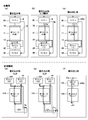
- 1A and 1B are a schematic diagram and an operation timing chart for describing a configuration of a nonvolatile flip-flop provided with a data write device for a resistance change type storage element of the present invention. It is a figure for demonstrating the structural example of a non-volatile flip-flop provided with the data writer of the resistance change type memory element of this invention. It is a figure for demonstrating the example of the signal of the Example of the non-volatile flip flop of this invention. 6 is a timing chart of an operation example of the data write device of the resistance change type storage element of the present invention. It is the schematic for demonstrating the data writing apparatus of the conventional resistance change type memory element.
- FIGS. 5 and 6 A schematic configuration of a resistance change memory element used in a writing device and a configuration example of the resistance change memory element will be described.
- the writing means and the output means included in the data writing device of the resistance change type memory element of the present invention will be described with reference to FIGS. 5 and 6, the control means will be described with reference to FIG. Will be described with reference to FIGS.
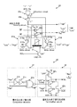
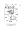
- FIG. 1 is a schematic configuration diagram for explaining a resistance change type memory element data writing apparatus according to the present invention.
- the resistance variable memory element data writing device 1 includes a variable resistance memory element 10, a writing unit 20, an output unit 30, and a control unit 40.
- the resistance change memory element 10 includes a conductive electrode 13 at one end of a memory element 11 that causes a resistance change, and a read electrode 12 at the other end.
- the memory element 11 changes resistance by flowing a write current through the conductive electrode 13 and stores data by associating the resistance change with data.
- the writing unit 20 includes a driving unit 21 that changes the resistance of the resistance change storage element 10 by switching the current direction of the write current to the conductive electrode 13 and writes to the storage element 11.
- the output means 30 is provided between the power supply (VDD) and the read electrode 12 of the storage element 11, and uses the read signal VRD from the storage element 11 and the monitor signal VM for monitoring the write state of the storage element 11 as output signals. Output.
- the control means 40 controls the driving means 21 based on the monitor signal VM from the output means 30 when writing to the resistance change type storage element 10, and stops the supply of the write current based on the write end detection.
- the output means 30 is provided between the power supply (VDD) and the read electrode 12, and the read signal VRD from the storage element 11 from the output means 30 and the monitor signal VM for monitoring the write state of the storage element 11 by the write means 20. Is output as an output signal.
- the current at the time of taking out the output signal (read signal VRD, monitor signal VM) by setting the output means 30 between the power source (VDD) and the read electrode 12.
- the path is formed by a path that is grounded via the power source (VDD), the output unit 30, the read electrode 12, the storage element 11, and the conductive electrode 13, while the current path of the write current at the time of writing is the write unit 20. And a path that returns to the writing means 20 again via one terminal of the conductive electrode 13, the conductive electrode 13, and the other terminal of the conductive electrode 13.
- the current path of the output signal and the current path of the write current are separated, and the output signal and the write current are output independently without interfering with each other. Since the output signal and the write current are independent, the output signal is acquired without being affected by the write current.
- the control means 40 includes a write end detector 41 and a write end signal generator 42.
- the write end detection unit 41 outputs a write end detection signal DONE based on the write signal Y from the write unit 20 and the monitor signal VM in the write state from the output unit 30.
- the write end signal generation unit 42 outputs a write end signal WE based on the write end detection signal DONE of the write end detection unit 41.
- the write end signal generation unit 42 controls the drive means 21 by the generated write end signal WE, and stops writing to the resistance change storage element 10.
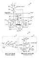
- FIG. 2 shows only components necessary for explanation in the schematic configuration shown in FIG. 1 according to the write operation and the read operation, and omits other portions.
- FIG. 2 (a) shows the operating state at the time of writing.
- a writing current is supplied from the writing means 20 to the conductive electrode 13 of the resistance change memory element 10.
- the direction of the write current is switched depending on data to be written.
- no current for obtaining an output signal flows through the output means 30 and the storage element 11.
- FIG. 2B shows an operation example when the write state of the memory element is monitored at the time of writing.
- a monitor current IM (broken line in the figure) is passed from the output means 30 via the readout electrode 12, the storage element 11, and the conductive electrode 13, and the output means 30 sets the monitor current IM and the resistance value of the storage element 11 to each other.
- a corresponding monitor signal VM is output.
- the monitor signal VM is a value corresponding to the resistance of the memory element 11, and the resistance value of the memory element 11 is a value corresponding to the written data. Therefore, the writing state of the memory element is monitored based on the monitor signal VM. .
- FIG. 2 (c) shows an operation state at the time of reading.
- a read current IR (broken line in the figure) is output from the output means 30 via the read electrode 12, the storage element 11, and the conductive electrode 13, and the output means 30 outputs a read signal VRD from the read current IR. Since the read signal VRD has a value corresponding to the resistance of the memory element 11, the storage state of the memory element 11 is read based on the read signal VRD.
- FIG. 19 is used as the configuration of the conventional writing means.
- 2 (d) and 2 (e) show the operating state during writing and monitoring of a conventional writing device.
- a writing current is supplied from the writing unit 120A or the writing unit 120B to the resistance change storage element 110.
- the write current is supplied from one writing unit to the resistance change storage element 110 and then flows to the other writing unit.
- the current direction from the writing unit 120A to the writing unit 120B or the current direction from the writing unit 120A to the writing unit 120B is selected as the writing current according to the writing data.
- the monitor detects a voltage on the terminal side to which a current is supplied to the resistance change storage element 110 as a monitor signal VM (a chain line in the figure). At this time, the monitor signal VM is selected according to the current direction of the write current by the multiplexer 121 based on the driven write means.
- FIG. 2 (f) shows an operation state at the time of reading.
- a read current IR (broken line in the figure) is supplied from the reading unit 130 to the resistance change storage element 110, and a read signal VRD is output. Since the read signal VRD has a value corresponding to the resistance of the resistance change storage element 110, the storage state of the resistance change storage element 110 is read based on the read signal VRD.
- the monitor signal VM when monitoring the writing state of the memory element, the monitor signal VM is detected using the monitor current IM flowing in the current path independent of the writing current path by the writing means.
- the monitor signal VM when monitoring the writing state of the storage element, the monitor signal VM is detected using the writing current flowing through the writing current path by the writing means. Since the detection position of the monitor signal VM differs depending on the current direction of the write current, the multiplexer 121 is required to switch and output the monitor signal.
- FIG. 3A shows a schematic configuration of the resistance change storage element 10.
- the resistance change memory element 10 includes a conductive electrode 13 at one end of a memory element 11 that causes a resistance change, and a read electrode 12 at the other end. A resistance change occurs in the memory element 11 by supplying a write current to the conductive electrode 13.
- the readout electrode 12 includes a terminal T1, and the conductive electrode 13 includes two terminals T2 and T3.
- the magnetization direction is changed, and the resistance RM of the memory element 11 is changed by this magnetization direction.
- FIG. 3B shows the hysteresis characteristics between the write current IWR and the resistance RM of the memory element 11.
- the high resistance R1 changes its resistance to the low resistance R0 by passing the write current IW1.
- the resistance of the memory element 11 of the resistance change type memory element 10 is the low resistance R0
- the low resistance R0 changes to the high resistance R1 by passing the write current IW2.
- Data writing to the storage element 11 is performed by passing a write current IWR between the terminals T2 and T3.
- reading of data from the storage element 11 is detected by the voltage at the terminal T1 obtained by the read current IR.
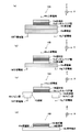
- FIGS. 4A to 4D are schematic cross-sectional views of the resistance change type memory elements 10A, 10B, 10C, and 10D, and show four configuration examples.
- the following configuration examples of the resistance change type storage elements 10A to 10C refer to the configuration example described in Patent Document 2, and are configuration examples using MTJ elements.
- a configuration example of the resistance change type storage element 10D refers to a configuration example described in Patent Document 3, and is a configuration example using a magnetization reversal type MTJ element using a spin orbit torque.
- FIG. 4A is a cross-sectional view showing a configuration example of the resistance change memory element 10A.
- the resistance change type storage element 10 has a configuration in which the magnetization state of the magnetization free layer is reversed by a magnetic field generated by a magnetization reversal current.
- the resistance change storage element 10A includes a conductive layer 10a, a magnetization fixed layer 10b, a tunnel barrier layer 10c, and a magnetization free layer 10d.
- the magnetization fixed layer 10b is formed directly on the upper surface of the conductive layer 10a
- the tunnel barrier layer 10c is formed on the upper surface of the magnetization fixed layer 10b.
- the magnetization free layer 10d is formed on the upper surface of the tunnel barrier layer 10c.
- the magnetization fixed layer 10b is formed of a ferromagnetic film whose magnetization is fixed, and the magnetization free layer 10d is formed of a ferromagnetic film whose magnetization can be reversed.
- the terminal 10f of the resistance change memory element 10A is provided near one end of the conductive layer 10a, and the terminal 10g is provided near the other end of the conductive layer 10a.
- the terminal 10e of the resistance change type storage element 10A is provided on the upper surface of the magnetization free layer 10d.
- the resistance change memory element 10A when a magnetization reversal current flows in the + X direction to the conductive layer 10a, a magnetic field is applied to the magnetization free layer 10d in the + Y direction, and thereby the magnetization directions of the magnetization fixed layer 10b and the magnetization free layer 10d Are parallel to each other, and the resistance change storage element 10A is in a low resistance state.
- a magnetization reversal current is passed through the conductive layer 10a in the -X direction
- a magnetic field is applied to the magnetization free layer 10d in the -Y direction, so that the magnetization directions of the magnetization fixed layer 10b and the magnetization free layer 10d are antiparallel.
- the resistance change storage element 10A enters a high resistance state.
- FIG. 4B shows another configuration example.
- the magnetization free layer 10d is directly stacked on the upper surface of the conductive layer 10a, and the tunnel barrier layer 10c is stacked on the upper surface of the magnetization free layer 10d.
- the magnetization fixed layer 10b may be stacked on the upper surface of the tunnel barrier layer 10c.
- the conductive layer 10a corresponds to the conductive electrode of the resistance change memory element of the present invention.
- the resistance change type storage element 10C is configured as a domain wall motion type MTJ element that reverses the magnetization of the magnetization free layer by the spin given to the electrons of the magnetization reversal current.
- the resistance change storage element 10C includes spin sources 10h and 10i, a magnetization free layer 10d, a tunnel barrier layer 10c, and a magnetization fixed layer 10b.
- the spin sources 10h and 10i are joined to the lower surfaces near both ends of the magnetization free layer 10d.
- the tunnel barrier layer 10c is stacked on the upper surface of the magnetization free layer 10d, and the magnetization fixed layer 10b is stacked on the upper surface of the tunnel barrier layer 10c.
- the magnetization direction is the vertical direction (Z-axis direction).
- the magnetization of the magnetization fixed layer 10b is fixed in the + Z direction.
- the magnetization of the spin source 10h is fixed in the ⁇ Z direction, and the magnetization of the spin source 10i is fixed in the + Z direction.
- the magnetization free layer 10d is divided into a region in which the magnetization is directed upward and a region in which the magnetization is directed downward, with a domain wall 10j generated between the spin source 10h and the spin source 10i as a boundary.
- the resistance change memory element 10C when a magnetization reversal current is passed in the + X direction, electrons spin-polarized by the spin source 10h are injected into the magnetization free layer 10d.
- the domain wall 10j moves in the ⁇ X direction by the spin torque action of the injected spin-polarized electrons and reaches the vicinity of the spin source 10h.
- the magnetization direction of the magnetization free layer 10d immediately below the magnetization fixed layer 10b is parallel to the magnetization fixed layer 10b, and the resistance change storage element 10C is in a low resistance state.
- the domain wall 10j near the spin source 10h moves in the + X direction and reaches the vicinity of the spin source 10i.
- the magnetization direction of the magnetization free layer 10d immediately below the magnetization fixed layer 10b is antiparallel to the magnetization fixed layer 10b, and the resistance change storage element 10C is in a high resistance state.
- the portion below the magnetization free layer 10d corresponds to the conductive electrode of the resistance change memory element of the present invention.
- the resistance change storage element 10D includes a heavy metal layer 10k having a shape made of heavy metal and extending in one direction, and a recording made of a ferromagnetic material and provided adjacent to the heavy metal layer 10k.
- a barrier layer 10m formed of an insulator and adjacent to a surface of the recording layer 10l opposite to the heavy metal layer 10k; a recording layer 10l of the barrier layer 10m; Is constituted by a reference layer 10n provided adjacent to the opposite surface.
- the reference layer 10n is a layer whose magnetization direction is fixed.
- the heavy metal layer 10k corresponds to the conductive electrode of the resistance change memory element of the present invention.
- the upper electrodes of the resistance change type storage elements 10A to 10C correspond to read electrodes of the resistance change type storage element of the present invention.
- the resistance change type storage element 10D a portion corresponding to the readout electrode of the resistance change type storage element of the present invention is not specified, but it is an electrode provided at the end of the storage element opposite to the conductive electrode. is there.
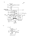
- the writing unit 20 includes a driving unit 21A and 21B for supplying a writing current to the conductive electrode 13 of the resistance change type memory element 10, and a control unit for forming a writing signal Y for causing the driving unit 21A and 21B to perform a writing operation. 22.
- the output of the inverter 22b of the control unit 22 is shown as the write signal Y as a write signal to the drive unit 21A, but the output of the inverter 22b of the control unit 22 is shown as the write signal to the drive unit 21B.
- the output of the NAND circuit 22a of the write signal circuit inverter 22b is used as a write signal.
- the control unit 22 includes a NAND circuit 22a and an inverter 22b.
- the output terminal of the inverter 22b is connected to the driving means 21A, and the input terminal of the inverter 22b is connected to the driving means 21B.
- the NAND circuit 22a receives the data signal Nq and the backup signal BCK.
- the backup signal BCK is a signal for performing processing after the data write operation
- the data signal Nq is a signal formed in synchronization with the clock CLK for writing the data D.
- the NAND 22a outputs “High” when both the backup signal BCK and the data signal Nq are “Low”, and when either the backup signal BCK or the data signal Nq is “Low” and the other is “High”, When the backup signal BCK and the data signal Nq are both “High”, “Low” is output.
- the inverter 22b inverts the output of the NAND circuit 22a and outputs it.
- the drive means 21A is composed of an inverter 21Ab and an NMOS transistor 21Aa.
- the inverter 22A of the control unit 22 is connected to the input terminal of the inverter 21Ab, the drain of the NMOS transistor 21Aa is connected to the output terminal of the inverter 21Ab, and the NMOS transistor 21Aa.
- the inverter 21Ab supplies a write current to one end of the conductive electrode 13 based on the write signal Y input from the inverter 22b of the control unit 22.
- the NMOS transistor 21Aa is turned off by the write end signal WE and ends the write operation.
- the driving means 21B is composed of an inverter 21Bb and an NMOS transistor 21Ba.
- the input terminal of the inverter 21Bb is connected to the output terminal of the NAND circuit 22a of the control unit 22, and the output terminal of the inverter 21Bb is connected to the drain of the NMOS transistor 21Ba.
- the source of the NMOS transistor 21Ba is connected to the other end of the conductive electrode 13.
- the inverter 21Bb supplies a write current to the other end of the conductive electrode 13 based on a write signal input from the NAND circuit 22a of the control unit 22.
- the drive means 21A is connected to one end of the conductive electrode 13, and the drive means 21B is connected to the other end of the conductive electrode 13, and is driven exclusively based on a write signal from the control unit 22, and the conductive electrode 13 Is supplied with the write current switched in the current direction.
- the NMOS transistor 21Ba is turned off by the write end signal WE to end the write operation. Note that one end of the conductive electrode 13 is grounded via the NMOS transistor 31.
- a read control signal RCL is input to the control terminal of the NMOS transistor 31, and one end of the conductive electrode 13 is grounded at the time of reading.
- the drive means 21 shown in FIG. 5B shows a configuration example of the drive means 21A and 21B.
- the drive means 21 is configured by connecting the output terminal of the inverter 21I to the drain of the NMOS transistor 21o, and the write end signal WE is input to the control terminal of the NMOS transistor 21o.
- the inverter 21I connects the drain of the PMOS transistor 21p and the drain of the NMOS transistor 21n to serve as an output terminal, connects the source of the PMOS transistor 21p to the power supply, grounds the source of the NMOS transistor 21n, and controls the control terminal of the PMOS transistor 21p.
- the control terminal of the NMOS transistor 21n is connected to serve as an input terminal.
- a write signal Y or an inverted signal of Y is input to the driving unit 21A, and an inverted Y signal or a write signal Y is input to the driving unit 21B.
- the driving means 21 the NMOS transistor 21n is turned on and the PMOS transistor 21p is turned off by the write signal Y in the “High” state or an inverted signal of Y. Since the transistor 21o is turned on by the write end signal WE in the “High” state, the write current IWR passes through the conductive electrode 13 and then flows to the ground side via the transistor 21a and the NMOS transistor 21n of the inverter 21I.
- One form of the output means 30 is constituted by a circuit in which a PMOS transistor 30b and an NMOS transistor 30a are connected in series.
- the power source (VDD) is connected to the source terminal of the PMOS transistor 30b
- the read electrode 12 of the memory element 11 is connected to the source terminal of the NMOS transistor 30a.
- a connection node between the drain end of the PMOS transistor 30b and the drain end of the NMOS transistor 30a is an output end for outputting the read signal VRD and the monitor signal VM.
- An inverted signal of the monitor control signal SE is connected to the control terminal of the PMOS transistor 30b connected to the power supply voltage VDD side, and the monitor control signal SE is connected to the control terminal of the NMOS transistor 30a connected to the read electrode 12 of the memory element 11.
- the monitor control signal SE is connected to the control terminal of the NMOS transistor 30a connected to the read electrode 12 of the memory element 11.
- a connection point between two transistors (PMOS transistor 30b, NMOS transistor 30a) is used as an output terminal to output read signals VRD and VM (signal A).
- the monitor control signal SE when the monitor control signal SE is “High”, the PMOS transistor 30b is in the off state and the NMOS transistor 30a is in the on state. Therefore, the read signal VRD and the monitor signal VM output from the output terminal are A voltage corresponding to the resistance of the memory element 11 is output. Note that when the monitor control signal SE is “Low”, the PMOS transistor 30b is in the on state and the NMOS transistor 30a is in the off state, so that the power supply voltage VDD is output from the output terminal.
- the circuit configuration in which the PMOS transistor 30b and the NMOS transistor 30a are connected in series outputs the resistance of the resistance change storage element as a voltage by using the PMOS transistor 30b as a load resistance.
- the voltage at the connection point between the PMOS transistor 30b and the NMOS transistor 30a corresponds to the intersection at which the load curve of the PMOS transistor 30b and the voltage-current characteristic curve of the resistance change type storage element including the NMOS transistor 30a intersect.
- the voltage at the connection point is output as an output signal.
- the voltage-current characteristic curve on the resistance change type storage element side is related to the current flowing during monitoring and can be determined without being restricted by the write current. Therefore, it is possible to set the voltage width of the margin of the detection voltage for identifying the voltage difference in the write state in the memory element to be large without being restricted by the write current.
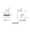
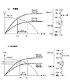
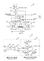
- FIG. 6 is a diagram for making a margin of a detection voltage for identifying a voltage difference in a write state in the memory element.
- FIG. 6A shows the case of the writing apparatus of the present invention
- FIG. 6B shows the case of the writing apparatus having the conventional configuration.
- the circuit shown on the right side schematically shows the circuit configuration of the memory element and the output means, and the left side shows the load characteristic curve and the voltage-current characteristic curve.
- the circuit configuration is divided into Part A and Part B with the output end as a boundary.
- PartA is a part corresponding to a PMOS transistor and serves as a load resistance.
- Part B is a portion corresponding to a memory element and an NMOS transistor.
- the voltage at the output terminal is a voltage at the intersection of the Part A load characteristic curve and the Part B voltage-current characteristic curve.
- FIG. 6A shows the relationship between the monitor current IM and the monitor signal VM flowing during monitoring, with respect to the load characteristic curve of Part A and the voltage-current characteristic curve of Part B.
- the voltage-current characteristic curve of Part B shows the case where the resistance RM of the written memory element is the low resistance R0 and the case of the high resistance R1, and the voltage determined at the intersection with the curve of the load characteristic of Part A is the monitor signal VM. Is output.
- the resistance RM of the memory element is the low resistance R0
- the voltage V0 is output as the monitor signal VM
- the resistance RM of the memory element is the high resistance R1
- the voltage V1 is output as the monitor signal VM.
- the writing state of the memory element is performed by determining whether the voltage value of the monitor signal VM is the voltage V0 or the voltage V1. In the determination of the monitor signal VM, the determination is easier as the voltage difference ⁇ V between the voltage V0 and the voltage V1 is larger and the voltage margin is larger, and can be identified by a low-sensitivity determination circuit. The smaller the voltage difference ⁇ V between the voltage V0 and the voltage V1 and the smaller the voltage margin, the more difficult the discrimination becomes, and a highly sensitive discrimination circuit is required.
- the margin of the voltage difference ⁇ V between the voltage V0 and the voltage V1 can be arbitrarily determined.
- the writing state of the memory element can be determined by a low-sensitivity determination circuit, and the circuit configuration of the determination circuit can be simplified and the size can be reduced.
- the load characteristic curve of Part A and the voltage-current characteristic curve of Part B show the relationship between the write current IWR that flows during writing and the write signal VBL.
- the voltage-current characteristic curve of Part B shows the case where the resistance RM of the written memory element is the low resistance R0 and the case of the high resistance R1, respectively.
- a voltage determined at the intersection with the curve of the load characteristic of Part A is output as the write signal VBL.
- the resistance RM of the memory element is the low resistance R0
- the voltage V0 is output as the monitor signal VM
- the resistance RM of the memory element is the high resistance R1
- the voltage V1 is output as the monitor signal VM.
- the intersection between the Part A load characteristic curve and the Part B voltage-current characteristic curve is restricted by the write current.
- a current higher than the write current IW0 is required, and in order to set the resistance RM of the memory element to the high resistance R1, a current higher than the write current IW1 is required. is there. Therefore, in the conventional configuration, the intersection of the curve of the load characteristic of Part A and the voltage-current characteristic curve of Part B is restricted by the write current, and the voltage V0 for writing the low resistance R0 and the voltage V1 for writing the high resistance R1 are also the write current IW0. And is restricted by the write current IW1.
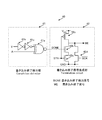
- FIG. 7 is a diagram for explaining a configuration example of the control means 40 of the present invention.
- the control means 40 includes a write end detection unit 41 and a write end signal generation unit 42.
- the write end detection unit 41 includes a negative exclusive OR 41a and an even number of inverters 41b and 41c. One input terminal of the negative exclusive OR 41a is controlled by an even number of inverters 41b and 41c.
- the write signal Y of the unit 22 is input, and the monitor signal VM (signal A) of the output means 30 is input to the other input terminal.
- the write end detection unit 41 detects the completion of the write process of the storage element 11 based on the coincidence of the write signal Y from the control unit 22 and the signal A of the output means 30, and outputs a write end detection signal DONE. .
- the write end signal generation unit 42 is a circuit that generates a write end signal WE based on the write end detection signal DONE of the write end detection unit 41.
- the write end signal generation unit 42 includes a series connection circuit in which three transistors 42a, 42b, and 42c are connected in series between the power supply voltage VDD and the ground voltage GND, and a parallel circuit that is connected in parallel to the transistors 42a and 42b. Composed.
- the transistor 42a is a PMOS transistor
- the transistors 42b, 42c, and 42d are NMOS transistors.
- a write end detection signal DONE which is an output signal of the write end detector 41, is input to the control gate of the transistor 42b, and a backup start control signal STR is input to the control gates of the transistors 42a and 42c. Note that the transistors 42a and 42c operate in an inverted state, and perform on / off operations in opposite directions with respect to the input of the backup start control signal STR.
- the backup start control signal STR becomes “Low” after switching from the normal operation to the backup operation, then becomes “High” after one clock cycle, and starts the backup operation.
- the write end detection signal DONE is in the “Low” state, and the write end detection signal DONE is in the “Low” state.
- the backup start control signal STR is switched from “Low” to “High”
- the transistor 42c is turned off and the transistor 32a is turned on.
- the write end detection unit 41 sets the write end detection signal DONE to “High”.
- the transistor 42b becomes “High” in response to the “High” state of the write end detection signal DONE, the transistors 42b and 42c are turned on, and the potential at the connection end of the drain of the transistor 42c and the drain of the transistor 42b becomes the ground potential. , “Low” write end signal WE is output.
- the transistor 42d is in an ON state by an inverted BCK obtained by inverting the backup signal BCK, and outputs a “Low” write end signal WE.
- the transistors 21Aa and 21Ba of the driving means 21A and 21B are turned off by the “Low” write end signal WE, and the write operation is completed.
- FIGS. 8 to 11 show the backup operation state 1 in which the data before and after the writing is different and the data is changed to different data depending on the writing.
- FIGS. 12 to 14 show the same data before and after the writing.
- the operation state 2 when not performing is shown.
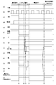
- Operation state 1 The timing chart shown in FIG. 8 shows a normal operation, a backup operation, a power-off state, and a read operation.
- the normal operation is an operation state in which data writing is not performed
- the backup operation is an operation state in which data writing and the data writing state are monitored
- the power-off stops the current supply to the storage element.
- the read operation is a state of reading data stored in the storage element.
- FIG. 8A shows the power supply VDD
- FIG. 8B shows the clock CLK
- FIG. 8C shows the enable signal EN that enables normal operation
- FIG. 8E shows the backup signal BCK for enabling the backup operation
- FIG. 8F shows the NAND output of the control unit 22
- FIG. 8G shows the output from the control unit 22.
- 8 (h) shows the storage state of the storage element 11
- FIG. 8 (i) shows the output signal A (read signal VRD, monitor signal VM) of the output means 30, and
- FIG. (J) shows a write end detection signal DONE for detecting the end of writing to the memory element
- FIG. 8 (k) shows a write end signal WE for stopping the write current
- FIG. 8 (l) shows a backup operation.
- FIG. 8 (m) shows the current IWR for writing to the memory element
- FIG. 8 (n) shows the read control signal RCL for controlling the read operation
- FIG. 8 (o) Indicates a monitor control signal SE for enabling the monitor.
- the normal operation is an operation state in which data is not written to the memory element while performing the same operation as the CMOS flip-flop when the enable signal EN is “High”.
- the resistance state of the memory element 11 is “Low”
- the write signal Y and the output signal A are both “Low”
- the write end detection signal DONE is “Low”. Is in a state.
- the data signal Nq changes from “Low” to “High” at the falling edge of any clock CLK during normal operation.
- (Backup operation) 9 and 10 show examples of operations of the writing means 20, the output means 30, and the control means 40 in the backup operation.
- Time A in FIG. 8 is a time when the normal operation is switched to the backup operation, and FIG. 9 shows an operation state at this time.
- the data write operation starts when the enable signal EN changes from “High” to “Low”, and the backup operation starts when the backup signal BCK changes from “Low” to “High”.
- the backup signal BCK and the data signal Nq are input to the NAND 22a, the NAND output becomes “Low” by switching the backup signal BCK, and the write signal Y is output from the inverter 22b. Further, in the control means 40, when the inverted signal of the backup signal BCK is switched to “High”, the transistor 42d is turned on, the write end signal WE becomes “High”, and the write operation becomes valid.
- the transistors 21Aa and 21Ba of the driving means 21A and 21B are changed from the off state to the on state by 30 write end signals WE, and the write current IWR is supplied to the conductive electrode 13 of the resistance change memory element 10.
- the transistors 30a and 30b of the output means 30 are in the on state, and the transistor 31 is switched on when the monitor control signal SE rises. However, since the resistance state is in the low resistance state, the output signal A is “Low”. ""
- Time B in FIG. 8 is a time point during which the backup start control signal STR is changed to “High” after one clock cycle after the backup start control signal STR becomes “Low” at the start of the backup operation.
- the write end signal generation unit 42 when the backup start control signal STR becomes “High”, the transistor 42a is turned on, and the transistor 42c is turned off. At this time, since the write end detection signal DONE is in the “Low” state, the transistor 42b is in the off state, and the write end signal WE is in the “High” state.
- Time C in FIG. 8 is a time when the resistance (data M) of the memory element 11 changes in the backup operation, and FIG. 10 shows an operation state at this time.
- the output signal A changes from “Low” to “High” in accordance with this change.
- the write end detection signal DONE of the write end detection unit 41 becomes “High”.
- the transistor 42b of the write end signal generator 42 is turned on in response to the write end detection signal DONE, and the write end signal WE is switched from “High” to “Low”.
- the transistors 21Aa and 21Ba of the driving means 21A and 21B are turned off when the write end signal WE is switched from “High” to “Low”, and the supply of the write current IWR is stopped.
- Time D in FIG. 8 is a time when the backup operation is switched to the power-off state. This operation is performed when the power supply (VDD) is turned off. In this power-off state, the resistance (data M) state is maintained. Note that in the case where a nonvolatile flip-flop is configured using a resistance change storage element, data disappearance due to a backup operation of the resistance change storage element and the power supply being turned off is avoided.
- Time E in FIG. 8 is a time at which the power is switched from the power-off state to the power-on state, and data written in the storage element is read out.
- FIG. 11 shows an operation state at this time point.
- the enable signal EN is in the “Low” state
- the backup signal is in the “Low” state
- the transistors 30a, 30b, and 31 are turned on by the rise of the read control signal RCL and the monitor control signal SE. Since the resistance (data M) of the memory element 11 is a high resistance, an output signal A of “High” is output from the output means 30.
- the write end detection unit 41 receives the output signal A in the “High” state and the write signal Y in the “Low” state, and the write end detection signal DONE outputs “Low”.
- the transistor 42b of the write end signal generation unit 42 is in the off state upon receiving the write end detection signal DONE, but the transistor 42d is turned on by the inverted signal of the backup signal, so the write end signal WE is maintained at “Low”.
- Operating state 2 The timing chart shown in FIG. 12 shows the normal operation, the backup operation, and the power-off state when the data before and after writing is the same and the data is not rewritten.
- the normal operation is an operation state in which no data is written
- the backup operation is an operation state in which the data writing and the data writing state are monitored
- the power-off presents a current supply to the storage element. State.
- FIG. 12 (a) shows the power supply VDD
- FIG. 12 (b) shows the clock CLK
- FIG. 12 (c) shows the enable signal EN for enabling normal operation
- FIG. FIG. 12E shows the backup signal BCK for enabling the backup operation
- FIG. 12F shows the NAND output of the control unit 22
- FIG. 12G shows the output from the control unit 22.
- 12 (h) shows the storage state of the storage element 11
- FIG. 12 (i) shows the output signal A (read signal VRD, monitor signal VM) of the output means 30, and
- FIG. (J) shows a write end detection signal DONE for detecting the end of writing to the storage element
- FIG. 12 (k) shows a write end signal WE for stopping the write current
- FIG. The backup start control signal STR for starting the up operation is shown
- FIG. 12 (m) shows the current IWR for writing to the memory element
- FIG. 12 (n) shows the monitor control signal SE for enabling the monitor. Yes.
- the normal operation is an operation state in which data writing is not performed due to the enable signal EN being “High”.
- the resistance state of the memory element 11 is “High” in response to the state of the timing chart of FIG. 8, and the write signal Y and the output signal A are both “Low”.
- the write end detection signal DONE is in the “Low” state, and the data signal Nq is maintained at “High”.
- FIGS. 13 and 14 show examples of operations of the writing means 20, the output means 30, and the control means 40 in the backup operation.
- Time F in FIG. 12 is a time when the normal operation is switched to the backup operation, and FIG. 13 shows an operation state at this time.
- the data write operation starts when the enable signal EN changes from “High” to “Low”, and the backup operation starts when the backup signal BCK changes from “Low” to “High”.
- the backup signal BCK and the data signal Nq are input to the NAND 22a, the NAND output becomes “Low” by switching the backup signal BCK, and the write signal Y is output from the inverter 22b. Further, in the control means 40, when the inverted signal of the backup signal BCK is switched to “High”, the transistor 42d is turned on, the write end signal WE becomes “High”, and the write operation becomes valid.
- the transistors 21Aa and 21Ba of the driving means 21A and 21B are changed from the off state to the on state by 30 write end signals WE, and the write current IWR is supplied to the conductive electrode 13 of the resistance change memory element 10.
- the transistors 30a and 30b of the output means 30 are in the on state, and the transistor 31 is switched to the on state when the monitor control signal SE rises, and the resistance state is in the high resistance state, so the output signal A is “High”. "”.
- the write end detection signal DONE is in the “High” state
- the write end signal WE is in the “High” state
- the write end control is not performed.
- control means lowers the backup start control signal STR in response to the write end detection signal DONE being in the “High” state.
- Time G in FIG. 12 is the end of writing in the backup operation, and FIG. 13 shows the operation state at this time.
- the write signal Y and the output signal A are “High” and the write end detection signal DONE is in the “High” state, but the control means receives the write end detection signal DONE and sets the backup start control signal STR. Therefore, the write end signal WE is switched from “High” to “Low” to control the write end, and the write current IWR ends in one cycle. From this operation, when the storage state of the storage element is the same as the storage state corresponding to the data to be written, the writing process is substantially skipped.
- the data write device of the resistance change type storage element of the present invention is applied to the master latch side in the configuration in which the master latch and the slave latch are continuously connected.
- the slave latch is assumed to be composed of a normal CMOS.
- a nonvolatile flip-flop (NV-FF) 50 includes a resistance change memory element, receives data D, and outputs an output Q at the timing of the clock CLK.
- the clock CLK, the enable signal EN, the data D, the backup signal BCK, the backup start control signal STR, and the read control signal RCL in FIG. 15 are signals similar to those described in the write device of the resistance change type memory element, and M Indicates the resistance state of the resistance change memory element.
- the reference numerals in the timing chart shown in FIG. 15 are the same as those in the timing charts shown in FIGS. 8 and 12 described in the resistance variable memory element writing device, and the data D input in the normal operation is the data in the backup operation. It is stored in the resistance state and output as an output Q, and is output as an output Q in a read operation (recall operation).
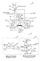
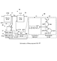
- FIG. 16 is a diagram showing a configuration example of a nonvolatile flip-flop (NV-FF) 50.
- the nonvolatile flip-flop (NV-FF) 50 is configured by continuously connecting a master latch 51 and a slave latch 52.
- the master latch 51 receives the data D and outputs a data signal Nq synchronized with the clock CLK to the slave latch 52.
- the master latch 51 stores the data signal Nq of the data D in the resistance change memory element 10 in the memory element 11 by the resistance change memory element writing device described above.
- the configuration example of the nonvolatile flip-flop (NV-FF) 50 in FIG. 16 is the same as the configuration of the writing device shown in FIG. 5 described above, the resistance change type storage element 10 and the writing unit 20 (driving unit (writing unit)). Driver) 21, control unit 22), and control means 40. Moreover, the control means 40 is provided with the write end detection part 41 and the write end signal generation part 42 as the structure similar to what was shown in FIG.
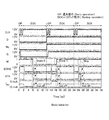
- FIG. 17 is an example of a signal of the embodiment of the nonvolatile flip-flop.
- the section from 0 ns to 12 ns and the section from 12 ns to 24 ns correspond to the operation state 1 described above, and the section from 24 ns to 36 ns corresponds to the operation state 2 described above. It corresponds to.
- Table 2 below shows a flip-flop having a CMOS configuration and a flip-flop having a configuration in which the resistance change type memory element applied to the present invention is used but the write current is not automatically stopped (Non-Patent Document 1, Table 2). Ref. [31]) and a flip-flop having a configuration in which a write current is automatically stopped using a resistance-change memory element having a conventional configuration (Ref. [19] in Non-Patent Document 2, Table 2). And power consumption [ ⁇ W], delay time [PS], and PDP [ ⁇ W * PS] (product of power consumption ⁇ W and delay time PS) for the flip-flop according to the configuration of the present invention.
- Table 2 the items shown in each row are, in order, volatile / non-volatile (NO is volatile, YES is non-volatile), and whether or not the writing process is automatically terminated (NO is no automatic termination, YES Indicates the presence of automatic termination), the number of transistors, power consumption ( ⁇ W), delay time (ps), and PDP (product of power consumption ⁇ W and delay time PS ( ⁇ W ⁇ ps)).
- (* 1) indicates that an input buffer, an output buffer, and a clock buffer are not included
- (* 2) indicates that the power supply voltage VDD is 1.2 V
- the CMOS is a 90 nm scale
- (* 3 ) Indicates the power consumption during normal operation at 1.0 GHz
- (* 4) indicates the maximum time from when the voltage VCLK of the clock CLK exceeds 50% until the voltage VQ of the output Q exceeds 50%.
- * 5) indicates PDP (product of power consumption ⁇ W and delay time PS).
- an 8-bit NV-FF is evaluated, and the switching time variation is 5 ns on average and the standard deviation is 10%. The time is 12 ns and the standard deviation is 12%.
- FIG. 18 shows a configuration using the resistance change type memory element applied to the present invention, in which the write current is automatically stopped (the dark graph in FIG. 18), and the write current is not automatically stopped. 18 shows a comparison of power consumption during the backup operation when the configuration is repeated 20 times for the configuration (light graph in FIG. 18).
- FIG. 18 confirms that the power consumption during backup is sufficiently reduced.
- Table 3 compares the average value of 100 times of backup energy in the normal configuration and the configuration of the present invention. According to this comparison, according to the configuration of the present invention, the backup energy is reduced by 69%.
- (* 1) indicates that the number of repetitions is 100
- (* 2) indicates that an arbitrary pattern is input
- (* 3) indicates that the pulse width of the write pulse is 12 ns. Show.
- the data write device of the resistance change type memory element of the present invention can be applied to logic elements such as flip-flops and nonvolatile memory devices.
- Resistance change type memory element writing device 10A, 10B, 10C, 10D Resistance change type memory element 10a Conductive layer 10b Magnetization fixed layer 10c Tunnel barrier layer 10d Magnetization free layer 10e, 10f, 10g Terminal 10h, 10i Spin source 10j Domain wall 10k Heavy metal layer 10l Recording layer 10m Barrier layer 10n Reference layer 11 Storage element 12 Read electrode 13 Conductive electrode 20 Write means 21, 21A, 21B Drive means 21Aa, 21Ba Transistor 21Ab, 21Bb Inverter 22 Controller 22a NAND circuit 22b Inverter 30 Output means 30a Transistor 30b Transistor 40 Control means 41 Write end detection section 41a Negative exclusive OR 41b, 41c IN Barter 42 Write end signal generation unit 42a, 42b, 42c, 42d Transistor 51 Master latch 52 Slave latch 100 Writing device 110 Resistance change type storage element 111 Storage element 120 Monitor unit 120A Writing means 120Aa Transistor 120Ab Writing driver 120B Writing means 120Ba Transistor 120Bb Write
Landscapes
- Engineering & Computer Science (AREA)
- Computer Hardware Design (AREA)
- Semiconductor Memories (AREA)
- Mram Or Spin Memory Techniques (AREA)
Abstract
抵抗変化を生じる記憶素子の一端に導電性電極、他端に読み出し電極を備え、導電性電極に電流を流すことにより記憶素子に抵抗変化を生じさせる抵抗変化型記憶素子において、抵抗変化型記憶素子へのデータの書き込みの終了を検出する。抵抗変化型記憶素子のデータ書き込み装置は、抵抗変化を生じる記憶素子の一端に導電性電極、他端に読み出し電極を備え、導電性電極に書き込み電流を流すことにより記憶素子に抵抗変化を生じさせる抵抗変化型記憶素子のデータ書き込み装置であり、書き込み手段と、出力手段と、制御手段とを備える。出力手段を電源と読み出し電極間に設け、出力手段から記憶素子からの読み出し信号、及び書き込み手段による記憶素子の書き込み状態をモニタするモニタ信号を出力信号として出力する。モニタ信号によって抵抗変化型記憶素子へのデータの書き込みの終了を検出する。
Description
本発明は、抵抗変化型記憶素子のデータ書き込み装置及び不揮発性フリップフロップに関する。
抵抗変化型記憶素子は、書き込み電流による抵抗状態を利用する記憶素子であるが、素子毎に抵抗状態が変化するタイミングにばらつきがあるため、抵抗変化型記憶素子への書き込み電流の供給には、記憶素子の抵抗変化状態を変化させるために十分な時間が求められる。そのため、抵抗変化型記憶素子の抵抗状態が変化した後においても記憶素子に書き込み電流を供給し続けるため、消費電力の点で課題を有している。
抵抗変化型記憶素子へのデータの書き込みの終了を検出する技術として、抵抗変化型記憶素子の端部電圧変化を書き込み電流の電流方向に応じて切り替えて検出し、検出した端部電圧変化に基づいてデータの書き込み終了を検出する装置が提案されている(特許文献1)。
抵抗変化型記憶素子を用いた不揮発性フリップフロップにおいて、抵抗変化型記憶素子のスイッチング動作時の電圧変化を検出し、書き込み電流の供給を終了することによってバックアップ電流を抑制する不揮発性フリップフロップ(self-terminated NV-FF)も提案されている(非特許文献1参照)。
上記の抵抗変化型記憶素子は、記憶素子の両端に書き込み電流用端子を備え、この電流用端子に対して書き込み電流を切り替えて供給する。これに対して、抵抗変化を生じる記憶素子の一端に導電性電極、他端に読み出し電極を備え、導電性電極に電流を流すことにより記憶素子に抵抗変化を生じさせる抵抗変化型記憶素子も提案されている(特許文献2)。
図19は従来から知られる抵抗変化型記憶素子の書き込み装置の構成例を示している。
書き込み装置100は、抵抗変化型の記憶素子111にデータ書き込むと共に、書き込み状態をモニタする書き込み/モニタ部120、及び記憶素子111に書き込んだデータを読み出す読み出し部130を備える。
書き込み/モニタ部120は、記憶素子111に対して書き込み電流を供給するトランジスタ120Aa及び書き込みドライバ120Ab、及びトランジスタ120Ba及び書き込みドライバ120Bbを備え、記憶素子111に対して互いに電流方向が逆方向の書き込み電流を供給すると共に、記憶素子111の両端の端子電圧(VM)をマルチプレクサ121で切り替えて出力することによって書き込み状態をモニタする。
読み出し部130は、PMOSトランジスタ130bのソースを電源に接続し、NMOSトランジスタ130aのソースを記憶素子111の一端に接続し、PMOSトランジスタ130bのドレインとNMOSトランジスタ130aのドレインを接続し、この接続点を出力端として、読み出し信号VRDを出力する。なお、記憶素子111の一端はNMOSトランジスタ122を介して接地される。NMOSトランジスタ122の制御端には読み出し制御信号RCLが入力される。
D,Suzuki,et al.,IEICE ELEX.11(2014) 20140296.
D,Suzuki,et al., J. Appl.Phys.,117(2015) 17B504.
特許文献2に示される形態の記憶素子の一端に導電性電極、他端に読み出し電極を備え、導電性電極に電流を流すことにより記憶素子に抵抗変化を生じさせる抵抗変化型記憶素子において、抵抗変化型記憶素子へのデータの書き込みの終了を検出する技術は提案されていない。
特許文献1に提案される抵抗変化型記憶素子へのデータの書き込みの終了を検出する技術を、特許文献2に示される形態の抵抗変化型記憶素子に適用することは構成上から困難性がある。特許文献2に示される形態の抵抗変化型記憶素子は、記憶素子の一端に設けた導電性電極に書き込み電流を供給し、記憶素子内に書き込み電流を導通させること無く書き込み動作を行う構成である。そのため、書き込み時においては記憶素子に書き込み電流が流れない。したがって、記憶素子の抵抗変化は記憶素子内を流れる電流を用いて検出するため、特許文献2に示される形態の抵抗変化型記憶素子の特許文献1の書き込み終了検出技術を適用し、書き込み電流に基づいてデータの書き込みの終了を検出することは構成上からできない。
そこで、本発明は前記した従来の問題点を解決し、抵抗変化を生じる記憶素子の一端に導電性電極、他端に読み出し電極を備え、導電性電極に電流を流すことにより記憶素子に抵抗変化を生じさせる抵抗変化型記憶素子において、抵抗変化型記憶素子へのデータの書き込みの終了を検出することを目的とする。
抵抗変化型記憶素子へのデータの書き込みの終了を検出することによって、バックアップ電流を抑制し、バックアップ処理における消費電力を低減することを目的とする。
本発明の抵抗変化型記憶素子のデータ書き込み装置は、抵抗変化を生じる記憶素子の一端に導電性電極、他端に読み出し電極を備え、この導電性電極に書き込み電流を流すことにより記憶素子に抵抗変化を生じさせる抵抗変化型記憶素子のデータ書き込み装置であり、書き込み手段と、出力手段と、制御手段とを備える。
書き込み手段は、導電性電極への書き込み電流の電流方向を切り替えることにより抵抗変化型記憶素子の抵抗変化を生じさせ、記憶素子に書き込みを行うと共に書き込み電流の供給を停止しうる駆動手段を備える。
出力手段は、電源と記憶素子の読み出し電極との間に設けられ、記憶素子からの読み出し信号、及び記憶素子の書き込み状態をモニタするモニタ信号を出力信号として出力する。
制御手段は、抵抗変化型記憶素子への書き込み時に、出力手段からのモニタ信号に基づいて駆動手段を制御する。
本発明は、出力手段を電源と読み出し電極間に設け、出力手段から記憶素子からの読み出し信号、及び書き込み手段による記憶素子の書き込み状態をモニタするモニタ信号を出力信号として出力する。この構成により、抵抗変化を生じる記憶素子の一端に導電性電極、他端に読み出し電極を備え、導電性電極に電流を流すことにより記憶素子に抵抗変化を生じさせる抵抗変化型記憶素子において、モニタ信号によって抵抗変化型記憶素子へのデータの書き込みが終了したことを検出する。
本発明の形態によれば、出力手段を電源と読み出し電極との間に設けることにより、出力信号の電流経路と、書き込み時における書き込み電流の電流経路とは分離した構成となる。出力信号の電流経路と書き込み電流の電流経路とが分離した構成は、出力信号を書き込み電流から独立して出力する。出力信号の電流経路と書き込み電流の電流経路とをそれぞれ独立した電流経路とすることで、出力信号は書き込み電流の影響を受けることなく取得される。
制御手段は、書き込み終了検出部と書き込み終了信号生成部とを備える。
書き込み終了検出部は、書き込み手段の書き込み信号と、書き込み状態を表す出力手段からのモニタ信号の2つの信号に基づいて、書き込み終了を検出して書き込み終了検出信号を出力する。書き込み終了信号生成部は、書き込み終了検出部の書き込み終了検出信号に基づいて書き込み終了信号を出力する。
書き込み終了検出部は、書き込み手段の書き込み信号と、書き込み状態を表す出力手段からのモニタ信号の2つの信号に基づいて、書き込み終了を検出して書き込み終了検出信号を出力する。書き込み終了信号生成部は、書き込み終了検出部の書き込み終了検出信号に基づいて書き込み終了信号を出力する。
書き込み終了信号生成部は、生成した書き込み終了信号によって駆動手段を制御し、モニタ信号に基づいて抵抗変化型記憶素子への書き込みを停止する。
出力手段の一形態は、PMOSトランジスタとNMOSトランジスタの直列回路で構成する。この回路構成において、PMOSトランジスタのソース端に電源が接続され、NMOSトランジスタのソース端に記憶素子の読み出し電極が接続される。PMOSトランジスタのドレイン端とNMOSトランジスタのドレイン端の接続ノードは、読み出し信号及びモニタ信号を出力する出力端である。
このPMOSトランジスタとNMOSトランジスタの直列回路による形態は、MOSトランジスタを負荷抵抗として用いて抵抗変化型記憶素子の抵抗を電圧信号として出力する。PMOSトランジスタとNMOSトランジスタとの接続点の電圧は、PMOSトランジスタによる負荷曲線と、NMOSトランジスタを含む抵抗変化型記憶素子の電圧-電流特性曲線とが交差する交点に対応する電圧であり、接続点の電圧を出力信号として出力する。
この出力手段の形態によれば、抵抗変化型記憶素子側の電圧-電流特性曲線は、モニタ時に流れる電流に関係するものであって、書き込み電流の制約を受けることなく定まるため、記憶素子の書き込み状態で相違する電圧を識別する際、両電圧間のマージンの電圧幅を大きく設定することが可能となる。検出電圧を識別する電圧のマージンを大きくすることで、記憶素子の書き込み状態の判別を低感度の判別回路で行うことができ、また、判別回路の回路構成を簡易化、及びサイズの小型化に寄与する。
また、書き込み電流路と読み出し電流路とが分離した構成であることから、出力手段と書き込み手段とを個別に最適化することができるため、論理回路の設計に好適である。
書き込み手段が備える駆動手段の一形態は、導電性電極の一端にソースを接続し、書き込み電流源側にドレインを接続する第1のNMOSトランジスタと、導電性電極の他端にソースを接続し、書き込み電流源側にインバータを介してドレインを接続する第2のNMOSトランジスタとを備え、第1のNMOSトランジスタ及び第2のNMOSトランジスタのゲートに制御手段からの書き込み終了信号を入力する。
抵抗変化型記憶素子の一形態は、記憶素子として3つの端子を備える抵抗変化型の磁気トンネル接合素子(MTJ素子:Magnetic Tunnel Jnction)を用いることができる。
本発明は不揮発性フリップフロップに適用することができ、マスターラッチとスレーブラッチとを継続接続して構成し、マスターラッチへのデータの書き込みに本発明の抵抗変化型記憶素子のデータ書き込み装置を適用する。
以上説明したように、本発明の抵抗変化型記憶素子のデータ書き込み装置は、抵抗変化を生じる記憶素子の一端に導電性電極、他端に読み出し電極を備え、導電性電極に電流を流すことにより記憶素子に抵抗変化を生じさせる抵抗変化型記憶素子において、抵抗変化型記憶素子へのデータの書き込みの終了を検出することができる。
また、本発明の抵抗変化型記憶素子のデータ書き込み装置は、抵抗変化型記憶素子へのデータの書き込みの終了を検出することによって、バックアップ電流を抑制し、バックアップ処理における消費電力を低減することができる。
以下、本発明の実施の形態について、図を参照しながら詳細に説明する。
以下、図1,2を用いて本発明の抵抗変化型記憶素子データの書き込み装置の概略構成、及び動作例を説明し、図3,4を用いて、本発明の抵抗変化型記憶素子のデータ書き込み装置に用いる抵抗変化型記憶素子の概略構成、及び抵抗変化型記憶素子の構成例を説明する。次に、本発明の抵抗変化型記憶素子のデータ書き込み装置が備える書き込み手段及び出力手段を図5,6を用いて説明し、制御手段を図7を用いて説明し、データ書き込み装置の動作例を図8~図14を用いて説明する。
以下、図1,2を用いて本発明の抵抗変化型記憶素子データの書き込み装置の概略構成、及び動作例を説明し、図3,4を用いて、本発明の抵抗変化型記憶素子のデータ書き込み装置に用いる抵抗変化型記憶素子の概略構成、及び抵抗変化型記憶素子の構成例を説明する。次に、本発明の抵抗変化型記憶素子のデータ書き込み装置が備える書き込み手段及び出力手段を図5,6を用いて説明し、制御手段を図7を用いて説明し、データ書き込み装置の動作例を図8~図14を用いて説明する。
更に、図15~図18を用いて本発明の抵抗変化型記憶素子のデータ書き込み装置を備えた不揮発性フリップフロップの構成例を説明する。
(抵抗変化型記憶素子のデータ書き込み装置の概略構成、及び動作)
図1は本発明の抵抗変化型記憶素子データの書き込み装置を説明するための概略構成図である。
図1は本発明の抵抗変化型記憶素子データの書き込み装置を説明するための概略構成図である。
抵抗変化型記憶素子のデータ書き込み装置1は、抵抗変化型記憶素子10、書き込み手段20、出力手段30、制御手段40を備える。
抵抗変化型記憶素子10は、抵抗変化を生じる記憶素子11の一端に導電性電極13、他端に読み出し電極12を備える。記憶素子11は、導電性電極13に書き込み電流を流すことにより抵抗変化させ、この抵抗変化をデータに対応付けることでデータを記憶させる。
書き込み手段20は、導電性電極13への書き込み電流の電流方向を切り替えることにより抵抗変化型記憶素子10の抵抗を変化させ、記憶素子11に書き込みを行う駆動手段21を備える。
出力手段30は、電源(VDD)と記憶素子11の読み出し電極12との間に設けられ、記憶素子11からの読み出し信号VRD、及び記憶素子11の書き込み状態をモニタするモニタ信号VMを出力信号として出力する。
制御手段40は、抵抗変化型記憶素子10への書き込み時に、出力手段30からのモニタ信号VMに基づいて駆動手段21を制御し、書き込み終了検出に基づいて書き込み電流の供給を停止する。
出力手段30は、電源(VDD)と読み出し電極12との間に設けられ、出力手段30から記憶素子11からの読み出し信号VRD、及び書き込み手段20による記憶素子11の書き込み状態をモニタするモニタ信号VMを出力信号として出力する。この構成により、導電性電極への電流供給により記憶素子に抵抗変化を生じさせる抵抗変化型記憶素子において、書き込み電流とは異なる電流経路によって検出されるモニタ信号VMによって記憶素子11へのデータの書き込みの終了を検出する。
出力時と書き込み時の電流経路についてみると、出力手段30の設置を電源(VDD)と読み出し電極12との間とすることにより、出力信号(読み出し信号VRD、モニタ信号VM)を取り出す際の電流経路は、電源(VDD)、出力手段30,読み出し電極12、記憶素子11、導電性電極13を介して接地される経路で形成され、一方、書き込み時における書き込み電流の電流経路は、書き込み手段20、導電性電極13の一方の端子、導電性電極13、導電性電極13の他方の端子を介して、再び書き込み手段20に戻る経路で形成される。
この構成によれば、出力信号の電流経路と、書き込み電流の電流経路とは分離した構成であり、出力信号と書き込み電流とはそれぞれ干渉することなく独立して出力される。出力信号と書き込み電流とが独立することで、出力信号を書き込み電流の影響を受けることなく取得される。
制御手段40は、書き込み終了検出部41と書き込み終了信号生成部42とを備える。書き込み終了検出部41は、書き込み手段20での書き込み信号Yと、出力手段30からの書き込み状態のモニタ信号VMとに基づいて書き込み終了検出信号DONEを出力する。一方、書き込み終了信号生成部42は、書き込み終了検出部41の書き込み終了検出信号DONEに基づいて書き込み終了信号WEを出力する。
書き込み終了信号生成部42は、生成した書き込み終了信号WEによって駆動手段21を制御し、抵抗変化型記憶素子10への書き込みを停止する。
次に、図2を用いて本発明の抵抗変化型記憶素子データの書き込み装置の動作を、従来の抵抗変化型記憶素子の書き込み装置の動作と比較して説明する。図2(a)~図2(c)は本発明の抵抗変化型記憶素子データの書き込み装置の動作を説明するための図であり、図2(d)~図2(f)は従来構成の抵抗変化型記憶素子データの書き込み装置の動作を説明するための図である。なお、図2は、図1に示した概略構成において、書き込み動作時及び読み出し動作時に応じて説明に要する構成部分のみを示し、その他の部分は省略している。
図2(a)は書き込み時の動作状態を示している。書き込み時には、書き込み手段20から抵抗変化型記憶素子10の導電性電極13に書き込み電流が供給される。書き込み電流は、書き込みを行うデータによって電流方向が切り替えられる。このとき、出力手段30及び記憶素子11には、出力信号を得るための電流は流れない。
図2(b)は、書き込み時において、記憶素子の書き込み状態をモニタする際の動作例を示している。モニタ時には、出力手段30から読み出し電極12、記憶素子11、及び導電性電極13を介してモニタ電流IM(図中の破線)を流し、出力手段30はモニタ電流IM及び記憶素子11の抵抗値に応じたモニタ信号VMを出力する。モニタ信号VMは記憶素子11の抵抗に応じた値であり、記憶素子11の抵抗値は書き込まれたデータに応じた値となるため、モニタ信号VMに基づいて記憶素子の書き込み状態がモニタされる。
図2(c)は読み出し時の動作状態を示している。読み出し時には、出力手段30から読み出し電極12、記憶素子11、及び導電性電極13を介して読み出し電流IR(図中の破線)をし、出力手段30は読み出し電流IRから読み出し信号VRDを出力する。読み出し信号VRDは記憶素子11に抵抗に応じた値となるため、読み出し信号VRDに基づいて記憶素子11の記憶状態が読み出される。
次に、図2(d)~図2(f)を用いて従来の書き込み装置の動作状態を説明する。なお、ここでは、従来の書き込み手段の構成として、図19に示した構成を用いている。
図2(d),(e)は従来の書き込み装置の書き込み時及びモニタ時の動作状態を示している。書き込み時及びモニタ時には、書き込み手段120A又は書き込み手段120Bから抵抗変化型記憶素子110に書き込み電流が供給される。書き込み電流は、一方の書き込み手段から抵抗変化型記憶素子110に供給された後、他方の書き込み手段に流れる。このとき、書き込み電流は、書き込みデータによって書き込み手段120Aから書き込み手段120Bへの電流方向、又は書き込み手段120Aから書き込み手段120Bへの電流方向が選択される。
モニタは、抵抗変化型記憶素子110に対して電流が供給される端子側の電圧をモニタ信号VM(図中の一点鎖線)として検出する。このとき、モニタ信号VMは、駆動される書き込み手段に基づいてマルチプレクサ121によって書き込み電流の電流方向に応じて選択される。
図2(f)は読み出し時の動作状態を示している。読み出し時には、読み出し部130から抵抗変化型記憶素子110に読み出し電流IR(図中の破線)を流して、読み出し信号VRDを出力する。読み出し信号VRDは抵抗変化型記憶素子110の抵抗に応じた値となるため、読み出し信号VRDに基づいて抵抗変化型記憶素子110の記憶状態が読み出される。
本発明の書き込み装置の形態によれば、記憶素子の書き込み状態をモニタする際に、書き込み手段による書き込み電流経路と独立した電流経路を流れるモニタ電流IMを用いてモニタ信号VMを検出する。一方、従来の書き込み装置の形態によれば、記憶素子の書き込み状態をモニタする際に、書き込み手段による書き込み電流経路を流れる書き込み電流を用いてモニタ信号VMを検出する。モニタ信号VMの検出位置は書き込み電流の電流方向で異なるため、モニタ信号を切り替えて出力するためにマルチプレクサ121が必要となる。
(抵抗変化型記憶素子の概略構成)
本発明の実施形態に用いられる抵抗変化型記憶素子10の構成について図3を参照して説明する。図3(a)は抵抗変化型記憶素子10の概略構成を示している。抵抗変化型記憶素子10は、抵抗変化を生じる記憶素子11の一端に導電性電極13、他端に読み出し電極12を備える。導電性電極13に書き込み電流を流すことにより記憶素子11に抵抗変化が生じる。
本発明の実施形態に用いられる抵抗変化型記憶素子10の構成について図3を参照して説明する。図3(a)は抵抗変化型記憶素子10の概略構成を示している。抵抗変化型記憶素子10は、抵抗変化を生じる記憶素子11の一端に導電性電極13、他端に読み出し電極12を備える。導電性電極13に書き込み電流を流すことにより記憶素子11に抵抗変化が生じる。
読み出し電極12は端子T1を備え、導電性電極13は2つの端子T2,T3とを備え、合わせて3端子を備える。導電性電極13の端子T2,T3間に流れる磁化反転電流の電流方向が反転すると磁化方向が変わり、この磁化方向によって記憶素子11の抵抗RMが変化する。
図3(b)は、書き込み電流IWRと記憶素子11の抵抗RMとのヒステリシス特性を示している。抵抗変化型記憶素子10の記憶素子11の抵抗が高抵抗R1の状態において、書き込み電流IW1を流すことによって高抵抗R1は低抵抗R0に抵抗変化する。一方、抵抗変化型記憶素子10の記憶素子11の抵抗が低抵抗R0の状態において、書き込み電流IW2を流すことによって低抵抗R0は高抵抗R1に抵抗変化する。例えば、高抵抗R1をデータM=1に対応させ、低抵抗R0をデータM=0に対応させることによって記憶素子として用いることができる。
記憶素子11のデータの書き込みは、端子T2,T3間に書き込み電流IWRを流すことで行う。一方、記憶素子11のデータの読み出しは、読み出し電流IRで得られる端子T1の電圧で検出する。
(抵抗変化型記憶素子の構成例)
次に、抵抗変化型記憶素子の構成例について、図4(a)~図4(d)を用いて概略構成を説明する。なお、ここで示す抵抗変化型記憶素子の構成例は一例であって、この構成に限られるものではない。
次に、抵抗変化型記憶素子の構成例について、図4(a)~図4(d)を用いて概略構成を説明する。なお、ここで示す抵抗変化型記憶素子の構成例は一例であって、この構成に限られるものではない。
図4(a)~(d)は抵抗変化型記憶素子10A,10B、10C、及び10Dの概略断面図であり、4つの構成例を示している。なお、下記の抵抗変化型記憶素子10A~10Cの構成例は特許文献2に記載される構成例を参照するものであり、MTJ素子による構成例である。また、抵抗変化型記憶素子10Dの構成例は特許文献3に記載される構成例を参照するものであり、スピン軌道トルクを用いた磁化反転方式のMTJ素子による構成例である。
図4(a)は抵抗変化型記憶素子10Aの一構成例を示す断面図である。抵抗変化型記憶素子10は磁化反転電流が発生する磁場により磁化自由層の磁化状態を反転させる構成を有している。図4(a)に示す構成例では、抵抗変化型記憶素子10Aは、導電層10aと、磁化固定層10bと、トンネルバリア層10cと、磁化自由層10dとを備え。磁化固定層10bは、導電層10aの上面に直接に形成され、トンネルバリア層10cは、磁化固定層10bの上面に形成される。磁化自由層10dは、トンネルバリア層10cの上面に形成される。磁化固定層10bは磁化が固定された強磁性体膜で形成され、磁化自由層10dは磁化が反転可能な強磁性体膜で形成される。抵抗変化型記憶素子10Aの端子10fは導電層10aの一方の端付近に設けられ、端子10gは導電層10aの他方の端付近に設けられる。抵抗変化型記憶素子10Aの端子10eは磁化自由層10dの上面に設けられる。
抵抗変化型記憶素子10Aは、磁化反転電流が導電層10aに+X方向に流れると、磁化自由層10dに+Y方向に磁界が印加され、これにより、磁化固定層10b及び磁化自由層10dの磁化方向が平行になり、抵抗変化型記憶素子10Aは低抵抗状態になる。一方、磁化反転電流が導電層10aに-X方向に流されると、磁化自由層10dに-Y方向に磁界が印加され、これにより、磁化固定層10b及び磁化自由層10dの磁化方向が反平行になり、抵抗変化型記憶素子10Aは高抵抗状態になる。
図4(b)は他の構成例を示している。抵抗変化型記憶素子10Bは、導電層10aの上面に磁化自由層10dが直接に積層され、磁化自由層10dの上面にトンネルバリア層10cが積層される。トンネルバリア層10cの上面に磁化固定層10bが積層される構成としてもよい。なお、図4(a)、図4(b)に示す構成の抵抗変化型記憶素子10A,10Bにおいて、導電層10aは本発明の抵抗変化型記憶素子の導電性電極に相当する。
図4(c)において、抵抗変化型記憶素子10Cは磁化反転電流の電子に与えられたスピンによって磁化自由層の磁化を反転させる磁壁移動型のMTJ素子として構成される。
抵抗変化型記憶素子10Cは、スピン源10h,10iと、磁化自由層10dと、トンネルバリア層10cと、磁化固定層10bとを備える。スピン源10h,10iは磁化自由層10dの両端付近の下面に接合される。トンネルバリア層10cは、磁化自由層10dの上面に積層され、磁化固定層10bはトンネルバリア層10cの上面に積層される。スピン源10h,10i、磁化自由層10d、磁化固定層10bは、何れも磁化方向が垂直方向(Z軸方向)である。磁化固定層10bの磁化は+Z方向に固定される。スピン源10hの磁化は-Z方向に固定され、スピン源10iの磁化は+Z方向に固定される。磁化自由層10dは、スピン源10hとスピン源10iの間に発生する磁壁10jを境界として磁化が上方向に向く領域と下方向に向く領域とに分かれる。
抵抗変化型記憶素子10Cは、磁化反転電流を+X方向に流すと、スピン源10hによってスピン偏極された電子が磁化自由層10dに注入される。この注入されたスピン偏極電子のスピントルク作用によって磁壁10jが-X方向に移動し、スピン源10hの近傍に到達する。その結果、磁化固定層10bの直下における磁化自由層10dの磁化方向は磁化固定層10bと平行になり、抵抗変化型記憶素子10Cは低抵抗状態となる。一方、磁化反転電流を-X方向に流すと、スピン源10h近傍にあった磁壁10jが+X方向へ移動し、スピン源10iの近傍に到達する。その結果、磁化固定層10b直下における磁化自由層10dの磁化方向は磁化固定層10bと反平行になり、抵抗変化型記憶素子10Cは高抵抗状態となる。なお、図4(c)に示す構成の抵抗変化型記憶素子10Cにおいて、磁化自由層10d以下の部分は本発明の抵抗変化型記憶素子の導電性電極に相当する。
図4(d)において、抵抗変化型記憶素子10Dは、重金属から構成され一方向に延伸された形状の重金属層10kと、強磁性体から構成され、重金属層10kに隣接して設けられた記録層10lと、絶縁体から構成され、記録層10lの重金属層10kとは反対側の面に隣接して設けられた障壁層10mと、強磁性体から構成され、障壁層10mの記録層10lとは反対側の面に隣接して設けられた参照層10nとにより構成される。
重金属層10kの長手方向(X軸方向)に書き込み電流が流され、この重金属層10kに流れる書き込み電流で発生するスピンによって、記録層10lの磁化方向が書き替えられる。また、参照層10nは、磁化方向が固定された層である。図4(d)に示す構成の抵抗変化型記憶素子10Dにおいて、重金属層10kは本発明の抵抗変化型記憶素子の導電性電極に相当する。
また、抵抗変化型記憶素子10A~10Cの上部電極は、本発明の抵抗変化型記憶素子の読み出し電極に相当している。抵抗変化型記憶素子10Dにおいて、本発明の抵抗変化型記憶素子の読み出し電極に相当する部分は明記されていないが、記憶素子に対して導電性電極とは反対側の端部に設けられる電極である。
(書き込み手段、及び出力手段の構成)
本発明の書き込み装置が備える書き込み手段20、及び出力手段30の構成例を図5を用いて説明する。
本発明の書き込み装置が備える書き込み手段20、及び出力手段30の構成例を図5を用いて説明する。
書き込み手段20は、抵抗変化型記憶素子10の導電性電極13に書き込み電流を供給する駆動手段21A及び21Bと、駆動手段21A,21Bに書き込み動作を行わせるための書き込み信号Yを形成する制御部22を備える。なお、図5では、駆動手段21Aへの書き込み信号として制御部22のインバータ22bの出力を書き込み信号Yとして示しているが、駆動手段21Bへの書き込み信号としては制御部22のインバータ22bの出力を書き込み信号回路インバータ22bのNAND回路22aの出力を書き込み信号として用いる。ここでは、これらの書き込み信号は符号のみがインバータ22bで反転されているだけであるので、書き込み状態の検出には一方の書き込み信号Yのみを検出すれば足りる。
制御部22は、NAND回路22a及びインバータ22bから構成され、インバータ22bの出力端は駆動手段21Aに接続され、インバータ22bの入力端は駆動手段21Bに接続される。
NAND回路22aには、データ信号Nqとバックアップ信号BCKが入力される。バックアップ信号BCKは、データの書き込み動作の後の処理を行わせるための信号であり、データ信号Nqは、データDを書き込むためにクロックCLKと同期して形成される信号である。NAND22aは、バックアップ信号BCKとデータ信号Nqが共に“Low”のとき、及びバックアップ信号BCKとデータ信号Nqの何れか一方が“Low”で他方が“High”のときに“High”を出力し、バックアップ信号BCKとデータ信号Nqが共に“High”のときは“Low”を出力する。インバータ22bはNAND回路22aの出力を反転して出力する。
駆動手段21Aは、インバータ21Ab及びNMOSトランジスタ21Aaから構成され、インバータ21Abの入力端には制御部22のインバータ22bが接続され、インバータ21Abの出力端にNMOSトランジスタ21Aaのドレインが接続され、NMOSトランジスタ21Aaのソースは導電性電極13の一端に接続される。インバータ21Abは、制御部22のインバータ22bから入力された書き込み信号Yに基づいて導電性電極13の一端に書き込み電流を供給する。NMOSトランジスタ21Aaは、書き込み終了信号WEによってOFF状態となり書き込み動作を終了させる。
一方、駆動手段21Bは、インバータ21Bb及びNMOSトランジスタ21Baから構成され、インバータ21Bbの入力端には制御部22のNAND回路22a出力端が接続され、インバータ21Bbの出力端にNMOSトランジスタ21Baのドレインが接続され、NMOSトランジスタ21Baのソースは導電性電極13の他端に接続される。インバータ21Bbは、制御部22のNAND回路22aから入力された書き込み信号に基づいて導電性電極13の他端に書き込み電流を供給する。駆動手段21Aは導電性電極13の一端に接続され、駆動手段21Bは導電性電極13の他端に接続され、制御部22からの書き込み信号に基づいてそれぞれ排他的に駆動し、導電性電極13に対して書き込み電流を電流方向を切り替えて供給する。NMOSトランジスタ21Baは、書き込み終了信号WEによってOFF状態となり書き込み動作を終了させる。なお、導電性電極13の一端はNMOSトランジスタ31を介して接地される。NMOSトランジスタ31の制御端には読み出し制御信号RCLが入力され、導電性電極13の一端は読み出し時に接地される。
図5(b)に示す駆動手段21は駆動手段21A,21Bの構成例を示している。駆動手段21は、NMOSトランジスタ21oのドレインにインバータ21Iの出力端を接続して構成され、NMOSトランジスタ21oの制御端には書き込み終了信号WEが入力される。
インバータ21Iは、PMOSトランジスタ21pのドレインとNMOSトランジスタ21nのドレインを接続して出力端とし、PMOSトランジスタ21pのソースを電源に接続し、NMOSトランジスタ21nのソースを接地し、PMOSトランジスタ21pの制御端とNMOSトランジスタ21nの制御端を接続して入力端とする。
例えば、書き込み時には、書き込み信号Y又はYの反転信号が駆動手段21Aに入力され、Yの反転信号又は、書き込み信号Yが駆動手段21Bに入力される。駆動手段21では、“High”状態にある書き込み信号Y又はYの反転信号によってNMOSトランジスタ21nはオン状態となり、PMOSトランジスタ21pはオフ状態となる。トランジスタ21oは、“High”状態の書き込み終了信号WEによってオン状態にあるため、書き込み電流IWRは導電性電極13を通過した後、トランジスタ21a及びインバータ21IのNMOSトランジスタ21nを介して接地側に流れる。
出力手段30の一形態は、PMOSトランジスタ30bとNMOSトランジスタ30aの直列接続した回路で構成する。この回路構成において、PMOSトランジスタ30bのソース端に電源(VDD)が接続され、NMOSトランジスタ30aのソース端に記憶素子11の読み出し電極12が接続される。PMOSトランジスタ30bのドレイン端とNMOSトランジスタ30aのドレイン端の接続ノードは、読み出し信号VRD及びモニタ信号VMを出力する出力端である。
電源電圧VDD側に接続されるPMOSトランジスタ30bの制御端にはモニタ制御信号SEの反転信号が接続され、記憶素子11の読み出し電極12に接続されるNMOSトランジスタ30aの制御端にはモニタ制御信号SEが接続され、2つのトランジスタ(PMOSトランジスタ30b、NMOSトランジスタ30a)の接続点を出力端とし読み出し信号VRD、VM(信号A)を出力する。
出力手段30は、モニタ制御信号SEが“High”の状態では、PMOSトランジスタ30bはオフ状態にあり、NMOSトランジスタ30aはオン状態にあるため、出力端から出力される読み出し信号VRD、モニタ信号VMは、記憶素子11の抵抗に応じた電圧が出力される。なお、モニタ制御信号SEが“Low”の状態では、PMOSトランジスタ30bはオン状態にあり、NMOSトランジスタ30aはオフ状態にあるため、出力端からは、電源電圧VDDが出力される。
PMOSトランジスタ30bとNMOSトランジスタ30aとを直列接続した回路構成の形態は、PMOSトランジスタ30bを負荷抵抗として用いることで抵抗変化型記憶素子の抵抗を電圧として出力する。PMOSトランジスタ30bとNMOSトランジスタ30aとの接続点の電圧は、PMOSトランジスタ30bによる負荷曲線と、NMOSトランジスタ30aを含む抵抗変化型記憶素子の電圧-電流特性曲線とが交差する交点に対応する電圧であり、接続点の電圧を出力信号として出力する。
この出力手段30の形態によれば、抵抗変化型記憶素子側の電圧-電流特性曲線は、モニタ時に流れる電流に関係し、書き込み電流の制約を受けることなく定めることができる。そのため、記憶素子に書き込み状態の電圧の違いを識別する検出電圧のマージンの電圧幅を、書き込み電流の制約を受けることなく大きく設定することが可能となる。
図6は記憶素子に書き込み状態の電圧の違いを識別する検出電圧のマージンをするための図である。図6(a)は本発明の書き込み装置の場合を示し、図6(b)は従来構成の書き込み装置の場合を示している。
図6(a)、(b)において、右側に示す回路は記憶素子及び出力手段の回路構成を概略して示し、左側は負荷特性曲線及び電圧-電流特性曲線を示している。回路構成において、出力端を境にして、PartAとPartBに分けられる。PartAは、PMOSトランジスタに相応する部分であり負荷抵抗となる。PartBは、記憶素子及びNMOSトランジスタに相当する部分である。
PartAとPartBには共通する電流が流れるため、出力端の電圧は、PartAの負荷特性の曲線とPartBの電圧-電流特性曲線とが交差する交点の電圧となる。
図6(a)は、PartAの負荷特性の曲線及びPartBの電圧-電流特性曲線について、モニタ時に流れるモニタ電流IMとモニタ信号VMとの関係を示している。
PartBの電圧-電流特性曲線は、書き込みされた記憶素子の抵抗RMが低抵抗R0の場合と高抵抗R1の場合を示し、それぞれPartAの負荷特性の曲線との交点で定まる電圧がモニタ信号VMとして出力される。記憶素子の抵抗RMが低抵抗R0の場合にはモニタ信号VMとして電圧V0が出力され、記憶素子の抵抗RMが高抵抗R1の場合にはモニタ信号VMとして電圧V1が出力される。
記憶素子の書き込み状態は、モニタ信号VMの電圧値が電圧V0であるかあるいは電圧V1であるかを判別することで行う。モニタ信号VMの判別において、電圧V0と電圧V1の電圧差ΔVが大きく、電圧のマージンが大きいほど判別が容易であり、低感度の判別回路で識別することができる。電圧V0と電圧V1の電圧差ΔVが小さく、電圧のマージンが小さいほど判別が難しくなり、高感度の判別回路が必要となる。
PartAの負荷特性の曲線はモニタ電流IMにより変更することができるため、電圧V0と電圧V1の電圧差ΔVのマージンを任意に定めることができる。マージンを大きくすることで、記憶素子の書き込み状態の判別を低感度の判別回路で行うことができ、また、判別回路の回路構成の簡易化、及びサイズの小型化に寄与することができる。
一方、従来構成では、図6(b)において、PartAの負荷特性の曲線及びPartBの電圧-電流特性曲線は、書き込み時に流れる書き込み電流IWRと書き込み信号VBLとの関係を示している。
図6(b)においても、図6(a)と同様に、PartBの電圧-電流特性曲線は、書き込みされた記憶素子の抵抗RMが低抵抗R0の場合と高抵抗R1の場合を示し、それぞれPartAの負荷特性の曲線との交点で定まる電圧が書き込み信号VBLとして出力される。記憶素子の抵抗RMが低抵抗R0の場合にはモニタ信号VMとして電圧V0が出力され、記憶素子の抵抗RMが高抵抗R1の場合にはモニタ信号VMとして電圧V1が出力される。
従来構成では、PartAの負荷特性の曲線とPartBの電圧-電流特性曲線との交点は書き込み電流の制約を受ける。記憶素子の書き込み動作では、記憶素子に書き込みを行うために所定値を超える書き込み電流を供給する必要があり、この書き込み電流は記憶素子に書き込む抵抗によって異なる。
例えば、記憶素子の抵抗RMを低抵抗R0とするには、書き込み電流IW0以上の電流が必要であり、記憶素子の抵抗RMを高抵抗R1とするには、書き込み電流IW1以上の電流が必要である。したがって、従来構成では、PartAの負荷特性の曲線とPartBの電圧-電流特性曲線との交点は書き込み電流の制約を受け、低抵抗R0を書き込む電圧V0と高抵抗R1を書き込む電圧V1も書き込み電流IW0及び書き込み電流IW1の制約を受ける。
このため、書き込み状態の判別に際して、低抵抗R0を判別する電圧V0と高抵抗R1を判別する電圧V1との電圧差ΔVを大きく設定することが難しく、電圧マージンが小さい。電圧マージンが小さいほど書き込み状態の判別が難しくなり、高感度の判別回路が必要となり、回路構成も大型化することになる。
(制御手段の構成)
図7は本発明の制御手段40の構成例を説明するための図である。
制御手段40は、書き込み終了検出部41と書き込み終了信号生成部42とを備える。書き込み終了検出部41は、否定排他的論理和41aと偶数個のインバータ41b,41cとから構成され、否定排他的論理和41aの一方の入力端子に偶数個のインバータ41b,41cを介して、制御部22の書き込み信号Yを入力し、他方の入力端子に出力手段30のモニタ信号VM(信号A)を入力する。書き込み終了検出部41は、制御部22からの書き込み信号Yと出力手段30の信号Aとの一致に基づいて記憶素子11の書き込み処理が完了したことを検出し、書き込み終了検出信号DONEを出力する。
書き込み終了信号生成部42は、書き込み終了検出部41の書き込み終了検出信号DONEに基づいて、書き込み終了信号WEを生成する回路である。書き込み終了信号生成部42は、電源電圧VDDと接地電圧GNDとの間に3つのトランジスタ42a,42b,及び42cを直列接続した直列接続回路と、トランジスタ42a及びトランジスタ42bに並列接続した並列回路とによって構成される。なお、ここでは、トランジスタ42aをPMOSトランジスタとし、トランジスタ42b,42c,及び42dをNMOSトランジスタとしている。
トランジスタ42bの制御ゲートには書き込み終了検出部41の出力信号である書き込み終了検出信号DONEが入力され、トランジスタ42a及び42cの制御ゲートにはバックアップ開始制御信号STRが入力される。なお、トランジスタ42a及びトランジスタ42cは互いに反転した状態で動作し、バックアップ開始制御信号STRの入力に対して互いに逆方向でオンオフ動作を行う。
バックアップ開始制御信号STRは、通常動作からバックアップ動作に切り替わる時点で“Low”となった後、1クロックサイクルの後に“High”となり、バックアップ動作を開始する。
バックアップ動作の開始時には、書き込み終了検出信号DONEは“Low”の状態にあり、書き込み終了検出信号DONEは“Low”の状態にある。バックアップ開始制御信号STRが“Low”から“High”に切り替わることにより、トランジスタ42cはオフ状態に、トランジスタ32aはオン状態となる。この状態において、出力手段30のモニタ信号VMによって信号Aが“High”となり、書き込み信号Yと共に“High”となると、書き込み終了検出部41は書き込み終了検出信号DONEは“High”とする。トランジスタ42bは、書き込み終了検出信号DONEの“High”状態を受けて“High”となり、トランジスタ42b,42cはオン状態となってトランジスタ42cのドレインとトランジスタ42bのドレインの接続端の電位は接地電位となり、“Low”の書き込み終了信号WEを出力する。
また、バックアップ動作を行わない期間は、トランジスタ42dはバックアップ信号BCKを反転した反転BCKによってオン状態にあり、“Low”の書き込み終了信号WEを出力する。駆動手段21A,21Bのトランジスタ21Aa,21Baは“Low”の書き込み終了信号WEによってオフ状態となる、書き込み動作が終了する。
(動作例)
次に、本発明の抵抗変化型記憶素子の書き込み装置の動作例を図8~図14を用いて説明する。なお、図8~図11は、書き込み前後のデータが異なり、書き込みによって異なるデータに書き替えるバックアップの動作状態1を示し、図12~図14は書き込み前後のデータが同じであり、データの書き替えが行われない場合の動作状態2を示している。
次に、本発明の抵抗変化型記憶素子の書き込み装置の動作例を図8~図14を用いて説明する。なお、図8~図11は、書き込み前後のデータが異なり、書き込みによって異なるデータに書き替えるバックアップの動作状態1を示し、図12~図14は書き込み前後のデータが同じであり、データの書き替えが行われない場合の動作状態2を示している。
動作状態1:
図8に示すタイミングチャートは、通常動作、バックアップ動作、電源オフの状態、及び読み出し動作を示している。ここで、通常動作は、データの書き込みを行わない動作状態であり、バックアップ動作は、データの書き込み及びデータの書き込み状態をモニタする動作状態であり、電源オフは記憶素子への電流供給を停止した状態であり、読み出し動作は、記憶素子に記憶されるデータを読み出す動作状態である。
図8に示すタイミングチャートは、通常動作、バックアップ動作、電源オフの状態、及び読み出し動作を示している。ここで、通常動作は、データの書き込みを行わない動作状態であり、バックアップ動作は、データの書き込み及びデータの書き込み状態をモニタする動作状態であり、電源オフは記憶素子への電流供給を停止した状態であり、読み出し動作は、記憶素子に記憶されるデータを読み出す動作状態である。
図8において、図8(a)は電源VDDを示し、図8(b)はクロックCLKを示し、図8(c)は通常動作を有効とするイネーブル信号ENを示し、図8(d)はデータ信号Nqを示し、図8(e)はバックアップ動作を有効にするバックアップ信号BCKを示し、図8(f)は制御部22のNAND出力を示し、図8(g)は制御部22から出力される書き込み信号Yを示し、図8(h)は記憶素子11の記憶状態を示し、図8(i)は出力手段30の出力信号A(読み出し信号VRD、モニタ信号VM)を示し、図8(j)は記憶素子への書き込みが終了したことを検出する書き込み終了検出信号DONEを示し、図8(k)は書き込み電流を停止させる書き込み終了信号WEを示し、図8(l)はバックアップ動作を開始するバックアップ開始制御信号STRを示し、図8(m)は記憶素子に書き込みを行うための電流IWRを示し、図8(n)は読み出し動作を制御する読み出し制御信号RCLを示し、図8(o)はモニタを有効にするモニタ制御信号SEを示している。
(通常動作)
通常動作は、イネーブル信号ENが“High”の状態によって、CMOSフリップフロップと同様の動作をしつつ、記憶素子へのデータの書き込みを行わない動作状態にある。なお、ここでは、記憶素子11の抵抗状態は“Low”の状態にあるものとし、書き込み信号Yと出力信号Aとは共に“Low”の状態にあり、書き込み終了検出信号DONEは“Low”の状態にある。また、通常動作中の何れかのクロックCLKの立ち下がりでデータ信号Nqが“Low”から“High”に変化したものとする。
通常動作は、イネーブル信号ENが“High”の状態によって、CMOSフリップフロップと同様の動作をしつつ、記憶素子へのデータの書き込みを行わない動作状態にある。なお、ここでは、記憶素子11の抵抗状態は“Low”の状態にあるものとし、書き込み信号Yと出力信号Aとは共に“Low”の状態にあり、書き込み終了検出信号DONEは“Low”の状態にある。また、通常動作中の何れかのクロックCLKの立ち下がりでデータ信号Nqが“Low”から“High”に変化したものとする。
(バックアップ動作)
図9,図10はバックアップ動作における書き込み手段20、出力手段30、及び制御手段40の動作例を示している。
図9,図10はバックアップ動作における書き込み手段20、出力手段30、及び制御手段40の動作例を示している。
(A時点) 図8のA時点は、通常動作からバックアップ動作に切り替わる時点であり、図9はこの時点の動作状態を示している。イネーブル信号ENが“High”から“Low”に変わることで、データの書き込み動作が開始され、バックアップ信号BCKが“Low”から“High”の状態に変わることでバックアップ動作が開始される。
NAND22aには、バックアップ信号BCK及びデータ信号Nqが入力され、バックアップ信号BCKの切り替わりによってNAND出力が“Low”となり、インバータ22bから書き込み信号Yが出力される。また、制御手段40において、バックアップ信号BCKの反転信号が“High”に切り替わることによって、トランジスタ42dがオン状態となって、書き込み終了信号WEが“High”となり、書き込み動作が有効となる。
駆動手段21A,21Bの各トランジスタ21Aa,21Baは30の書き込み終了信号WEによってオフ状態からオン状態に変わり、抵抗変化型記憶素子10の導電性電極13に対して書き込み電流IWRが供給される。
また、出力手段30のトランジスタ30a,30bはオン状態にあり、トランジスタ31はモニタ制御信号SEが立ち上がることでオン状態に切り替わるが、抵抗状態は低抵抗の状態にあるため、出力信号Aは“Low”の状態にある。
書き込み信号Yは“High”であるが出力信号Aは“Low”の状態にあるため、書き込み終了検出信号DONEは依然として“Low”の状態にあり、書き込み終了信号WEは“High”の状態のままであり、書き込み終了の制御は行われない。
(B時点) 図8のB時点は、バックアップ動作中においてバックアップ開始制御信号STRが、バックアップ動作開始で“Low”となった後、1クロックサイクルの後に“High”に切り替わる時点である。
書き込み終了信号生成部42において、バックアップ開始制御信号STRが“High”となることによって、トランジスタ42aはオン状態となるトランジスタ42cはオフ状態となる。このとき、書き込み終了検出信号DONEは“Low”状態にあるため、トランジスタ42bはオフ状態にあり、書き込み終了信号WEは“High”の状態にある。
(C時点) 図8のC時点は、バックアップ動作において記憶素子11の抵抗(データM)が変化する時点であり、図10はこの時点の動作状態を示している。
記憶素子11の抵抗(データM)が“Low”から“High”に変化すると、この変化に応じて出力信号Aが“Low”から“High”に切り替わる。この出力信号Aの変化に伴って、書き込み終了検出部41の書き込み終了検出信号DONEは“High”となる。書き込み終了信号生成部42のトランジスタ42bは書き込み終了検出信号DONEを受けてオン状態となって、書き込み終了信号WEは“High”から“Low”に切り替わる。
駆動手段21A,21Bのトランジスタ21Aa、21Baは、書き込み終了信号WEが“High”から“Low”に切り替わることでオフ状態となり、書き込み電流IWRの供給は停止される。
(電源オフ状態)
(D時点) 図8のD時点は、バックアップ動作から電源オフの状態に切り替わる時点である。この動作は、電源(VDD)がオフ状態となることで行われる。この電源オフの状態において、抵抗(データM)の状態は維持される。なお、抵抗変化型記憶素子を用いて不揮発性フリップフロップを構成では、抵抗変化型記憶素子をバックアップ動作させて電源がオフ状態となることによるデータの消滅を避ける。
(D時点) 図8のD時点は、バックアップ動作から電源オフの状態に切り替わる時点である。この動作は、電源(VDD)がオフ状態となることで行われる。この電源オフの状態において、抵抗(データM)の状態は維持される。なお、抵抗変化型記憶素子を用いて不揮発性フリップフロップを構成では、抵抗変化型記憶素子をバックアップ動作させて電源がオフ状態となることによるデータの消滅を避ける。
(読み出し動作)
(E時点) 図8のE時点は、電源オフから電源オンの状態に切り替わると共に、記憶素子に書き込まれたデータを読み出す時点であり、図11はこの時点の動作状態を示している。
(E時点) 図8のE時点は、電源オフから電源オンの状態に切り替わると共に、記憶素子に書き込まれたデータを読み出す時点であり、図11はこの時点の動作状態を示している。
この時点では、イネーブル信号ENは“Low”の状態にあり、バックアップ信号は“Low”の状態にある。
読み出し制御信号RCLおよびモニタ制御信号SEの立ち上がりによって、トランジスタ30a、30b、及び31はオン状態となる。記憶素子11の抵抗(データM)が高抵抗であるため、出力手段30から“High”の出力信号Aが出力される。書き込み終了検出部41は、“High”状態の出力信号Aと“Low”状態の書き込み信号Yとを受けて、書き込み終了検出信号DONEは“Low”を出力する。書き込み終了信号生成部42のトランジスタ42bは書き込み終了検出信号DONEを受けてオフ状態にあるが、トランジスタ42dはバックアップ信号の反転信号によってオン状態となるため、書き込み終了信号WEは“Low”が維持される。
動作状態2:
図12に示すタイミングチャートは、書き込み前後のデータが同じでありデータの書き替えが行われない場合において、通常動作、バックアップ動作、及び電源オフの状態を示している。ここで、通常動作は、データの書き込みを行わない動作状態であり、バックアップ動作は、データの書き込み及びデータの書き込み状態をモニタする動作状態であり、電源オフは記憶素子への電流供給を呈した状態である。
図12に示すタイミングチャートは、書き込み前後のデータが同じでありデータの書き替えが行われない場合において、通常動作、バックアップ動作、及び電源オフの状態を示している。ここで、通常動作は、データの書き込みを行わない動作状態であり、バックアップ動作は、データの書き込み及びデータの書き込み状態をモニタする動作状態であり、電源オフは記憶素子への電流供給を呈した状態である。
図12において、図12(a)は電源VDDを示し、図12(b)はクロックCLKを示し、図12(c)は通常動作を有効とするイネーブル信号ENを示し、図12(d)はデータ信号Nqを示し、図12(e)はバックアップ動作を有効にするバックアップ信号BCKを示し、図12(f)は制御部22のNAND出力を示し、図12(g)は制御部22から出力される書き込み信号Yを示し、図12(h)は記憶素子11の記憶状態を示し、図12(i)は出力手段30の出力信号A(読み出し信号VRD、モニタ信号VM)を示し、図12(j)は記憶素子への書き込みが終了したことを検出する書き込み終了検出信号DONEを示し、図12(k)は書き込み電流を停止させる書き込み終了信号WEを示し、図12(l)はバックアップ動作を開始するバックアップ開始制御信号STRを示し、図12(m)は記憶素子に書き込みを行うための電流IWRを示し、図12(n)はモニタを有効にするモニタ制御信号SEを示している。
(通常動作)
通常動作は、イネーブル信号ENが“High”の状態によって、データの書き込みを行わない動作状態にある。なお、ここでは、記憶素子11の抵抗状態は、図8のタイミングチャートの状態を受けて“High”の状態にあるものとし、書き込み信号Yと出力信号Aとは共に“Low”の状態にあり、書き込み終了検出信号DONEは“Low”の状態にあり、データ信号Nqは“High”を維持しているものとする。
通常動作は、イネーブル信号ENが“High”の状態によって、データの書き込みを行わない動作状態にある。なお、ここでは、記憶素子11の抵抗状態は、図8のタイミングチャートの状態を受けて“High”の状態にあるものとし、書き込み信号Yと出力信号Aとは共に“Low”の状態にあり、書き込み終了検出信号DONEは“Low”の状態にあり、データ信号Nqは“High”を維持しているものとする。
(バックアップ動作)
図13,図14はバックアップ動作における書き込み手段20、出力手段30、及び制御手段40の動作例を示している。
図13,図14はバックアップ動作における書き込み手段20、出力手段30、及び制御手段40の動作例を示している。
(F時点) 図12のF時点は、通常動作からバックアップ動作に切り替わる時点であり、図13はこの時点の動作状態を示している。
イネーブル信号ENが“High”から“Low”に変わることで、データの書き込み動作が開始され、バックアップ信号BCKが“Low”から“High”の状態に変わることでバックアップ動作が開始される。
イネーブル信号ENが“High”から“Low”に変わることで、データの書き込み動作が開始され、バックアップ信号BCKが“Low”から“High”の状態に変わることでバックアップ動作が開始される。
NAND22aには、バックアップ信号BCK及びデータ信号Nqが入力され、バックアップ信号BCKの切り替わりによってNAND出力が“Low”となり、インバータ22bから書き込み信号Yが出力される。また、制御手段40において、バックアップ信号BCKの反転信号が“High”に切り替わることによって、トランジスタ42dがオン状態となって、書き込み終了信号WEが“High”となり、書き込み動作が有効となる。
駆動手段21A,21Bの各トランジスタ21Aa,21Baは30の書き込み終了信号WEによってオフ状態からオン状態に変わり、抵抗変化型記憶素子10の導電性電極13に対して書き込み電流IWRが供給される。
また、出力手段30のトランジスタ30a,30bはオン状態にあり、トランジスタ31はモニタ制御信号SEが立ち上がることでオン状態に切り替り、抵抗状態が高抵抗の状態にあるため、出力信号Aは“High”の状態となる。
書き込み信号Y及び出力信号Aは“High”であるため、書き込み終了検出信号DONEは“High”状態となり、書き込み終了信号WEは“High”状態となり、書き込み終了の制御は行われない。
このとき、制御手段は、書き込み終了検出信号DONEが“High”状態となることを受けてバックアップ開始制御信号STRを立ち下げる。
(G時点) 図12のG時点は、バックアップ動作における書き込み終了の時点であり、図13はこの時点の動作状態を示している。
この時点において、書き込み信号Y及び出力信号Aは“High”であり、書き込み終了検出信号DONEは“High”状態であるが、制御手段は書き込み終了検出信号DONEを受けてバックアップ開始制御信号STRを立ち下げるため、書き込み終了信号WEは“High”から“Low”状態に切り替わって書き込み終了の制御が行われ、書き込み電流IWRは1サイクルで終了する。この動作から、記憶素子の記憶状態が書き込みを行うデータに対応する記憶状態と同じ場合には、書き込み処理が実質的にスキップされる。
(不揮発性フリップフロップの構成)
次に、本発明の抵抗変化型記憶素子の書き込み装置を用いた不揮発性フリップフロップの構成例について図15~図18を用いて説明する。
次に、本発明の抵抗変化型記憶素子の書き込み装置を用いた不揮発性フリップフロップの構成例について図15~図18を用いて説明する。
なお、ここでは、マスターラッチとスレーブラッチとを継続接続して構成において、マスターフラッチ側に本発明の抵抗変化型記憶素子のデータ書き込み装置を適用した例を示している。スレーブラッチについては通常のCMOSで構成したものとする。
図15において、本発明の不揮発性フリップフロップ(NV-FF)50は、抵抗変化型記憶素子を備え、データDを入力し、クロックCLKのタイミングで出力Qを出力する。図15中のクロックCLK、イネーブル信号EN、データD、バックアップ信号BCK、バックアップ開始制御信号STR、読み出し制御信号RCLは、抵抗変化型記憶素子の書き込み装置で説明したものと同様に信号であり、Mは抵抗変化型記憶素子の抵抗状態を示している。
図15中に示すタイミングチャート中の符号は抵抗変化型記憶素子の書き込み装置で説明した図8,及び図12で示したタイミングチャートと同様であり、通常動作において入力されたデータDはバックアップ動作において抵抗状態で記憶されると共に出力Qとして出力され、読み出し動作(リコール動作)において出力Qとして出力される。
図16は不揮発性フリップフロップ(NV-FF:Nonvolatile Flip-Flop)50の一構成例を示す図である。不揮発性フリップフロップ(NV-FF)50は、マスターラッチ51とスレーブラッチ52とを継続接続して構成される。
マスターラッチ51はデータDを入力し、クロックCLKに同期させたデータ信号Nqをスレーブラッチ52に出力する。マスターラッチ51は、前記で説明した抵抗変化型記憶素子の書き込み装置によってデータDのデータ信号Nqを抵抗変化型記憶素子10に記憶素子11に記憶する。
図16の不揮発性フリップフロップ(NV-FF)50の構成例は、前記した図5に示したものと同様の書き込み装置の構成として、抵抗変化型記憶素子10,書き込み手段20(駆動手段(書き込みドライバ)21,制御部22)、及び制御手段40を備える。また、制御手段40は、図7に示したものと同様の構成として、書き込み終了検出部41及び書き込み終了信号生成部42を備える。
(消費電力の比較)
次に、本発明の構成と従来構成とついて消費電力の比較例を示す。
本発明の不揮発性フリップフロップの例は、以下の表1に示すパラメータの抵抗変化型記憶素子を用い、90nmルールで設計している。

次に、本発明の構成と従来構成とついて消費電力の比較例を示す。
本発明の不揮発性フリップフロップの例は、以下の表1に示すパラメータの抵抗変化型記憶素子を用い、90nmルールで設計している。
図17は、不揮発性フリップフロップの実施例の信号の例であり、0nsから12nsの区間及び12nsから24nsの区間は前記した動作状態1に対応し、24nsから36nsの区間は上記した動作状態2に対応している。
図17によれば、データの書き込み、及びデータ書き込み後に書き込み電流の終了処理が成されていることが確認される。また、記憶素子においてNq=Mの場合には書き込み処理がスキップされていることが確認される。
また、以下の表2は、CMOS構成のフリップフロップと、本発明に適用した抵抗変化型記憶素子を用いているが書き込み電流の自動停止を行わない構成のフリップフロップ(非特許文献1、表2中でRef.[31]で表記)と、従来構成の抵抗変化型記憶素子を用いて書き込み電流の自動停止を行った構成のフリップフロップ(非特許文献2、表2中でRef.[19]で表記)と、本発明の構成によるフリップフロップについて、消費電力[μW]、遅延時間[PS]、及び、PDP[μW*PS](消費電力μWと遅延時間PSの積)を示している。
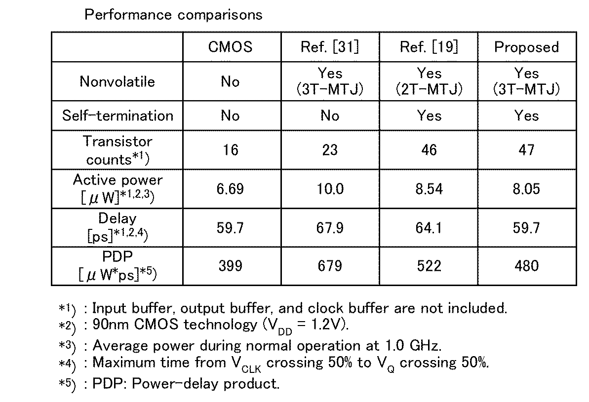
なお、上記表2において、各行に示す項目は順に、揮発性/不揮発性の有無(NOは揮発性、YESは不揮発性を示す)、書き込み処理の自動終了の有無(NOは自動終了無し、YESは自動終了有りを示す)、トランジスタ数、消費電力(μW)、遅延時間(ps)、及びPDP(消費電力μWと遅延時間PSの積(μW・ps))を示している。
また、(*1)は入力バッファ、出力バッファ、クロックバッファは含まれていないことを示し、(*2)は電源電圧VDDを1.2Vとし90nmスケールのCMOSであることを示し、(*3)は1.0GHzにおける通常動作中の消費電力を示し、(*4)はクロックCLKの電圧VCLKが50%を超えてから出力Qの電圧VQが50%を超えるまでの最大時間を示し、(*5)はPDP(消費電力μWと遅延時間PSの積)を示している。
この比較によれば、消費電力μWと遅延時間PSの積で表されるPDPは他の構成と比較して低減されることが確認される。
なお、実施例のフリップフロップでは、8ビットのNV-FFについて評価しており、スイッチング時間のばらつきは、平均のスイッチング時間が5nsで標準偏差は10%であり、最もばらつきが大きい場合にはスイッチング時間が12nsで標準偏差は12%である。
図18は、本発明に適用した抵抗変化型記憶素子を用いた構成において、書き込み電流の自動停止を行った本発明の構成(図18中の濃いグラフ)と、書き込み電流の自動停止を行わなかった構成(図18中の淡いグラフ)とについて20回繰り返した場合のバックアップ動作時の消費電力を比較して示している。
図18によれば、バックアップ時の消費電力が十分に低減されていることが確認される。
また、表3は、通常構成と本発明の構成とにおいて、バックアップエネルギーの100回の平均値を比較している。この比較によれば、本発明の構成によればバックアップエネルギーは69%の削減がされている。
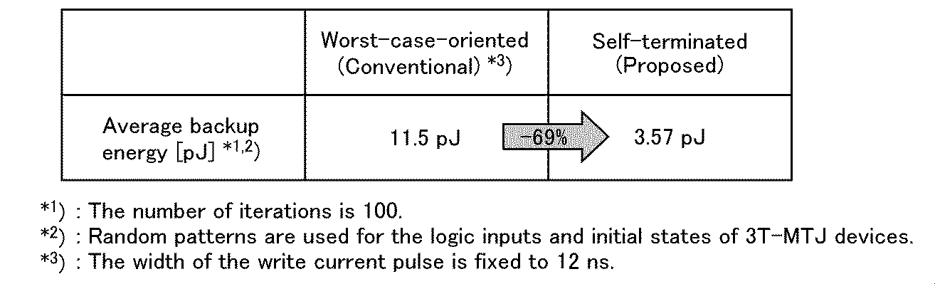
なお、(*1)は繰り返し回数が100回であることを示し、(*2)は任意のパターンの入力であることを示し、(*3)は書き込みパルスにパルス幅は12nsであることを示している。
なお、本発明は前記各実施の形態に限定されるものではない。本発明の趣旨に基づいて種々変形することが可能であり、これらを本発明の範囲から排除するものではない。
本発明の抵抗変化型記憶素子のデータ書き込み装置は、フリップフロップ、不揮発性記憶装置等の論理素子に適応することができる。
1 抵抗変化型記憶素子の書き込み装置
10,10A,10B,10C,10D 抵抗変化型記憶素子
10a 導電層
10b 磁化固定層
10c トンネルバリア層
10d 磁化自由層
10e,10f,10g 端子
10h,10i スピン源
10j 磁壁
10k 重金属層
10l 記録層
10m 障壁層
10n 参照層
11 記憶素子
12 読み出し電極
13 導電性電極
20 書き込み手段
21,21A,21B 駆動手段
21Aa,21Ba トランジスタ
21Ab,21Bb インバータ
22 制御部
22a NAND回路
22b インバータ
30 出力手段
30a トランジスタ
30b トランジスタ
40 制御手段
41 書き込み終了検出部
41a 否定排他的論理和
41b,41c インバータ
42 書き込み終了信号生成部
42a,42b,42c、42d トランジスタ
51 マスターラッチ
52 スレーブラッチ
100 書き込み装置
110 抵抗変化型記憶素子
111 記憶素子
120 モニタ部
120A 書き込み手段
120Aa トランジスタ
120Ab 書き込みドライバ
120B 書き込み手段
120Ba トランジスタ
120Bb 書き込みドライバ
121 マルチプレクサ
130 読み出し部
130a NMOSトランジスタ
130b PMOSトランジスタ
BCK バックアップ信号
CLK クロック
D データ
DONE 書き込み終了検出信号
EN イネーブル信号
GND 接地電圧
IM モニタ電流
IR 読み出し電流
IW0,IW1,IW2 書き込み電流
IWR 書き込み電流
M データ
Nq データ信号
Q 出力
R0 低抵抗
R1 高抵抗
RCL 読み出し制御信号
RM 抵抗
SE モニタ制御信号
STR バックアップ開始制御信号
T1,T2,T3 端子
VBL 書き込み信号
VDD 電源電圧
VM モニタ信号
VRD 読み出し信号
WE 書き込み終了信号
Claims (5)
- 抵抗変化を生じる記憶素子の一端に導電性電極、他端に読み出し電極を備え、前記導電性電極に書き込み電流を流すことにより前記記憶素子に抵抗変化を生じさせる抵抗変化型記憶素子のデータ書き込み装置であって、
書き込み手段と、
記憶素子からの読み出し信号、及び書き込み手段による記憶素子の書き込み状態をモニタするモニタ信号を出力する出力手段と、
制御手段と、
を備え、
前記書き込み手段は、前記導電性電極への書き込み電流の電流方向を切り替えることにより前記抵抗変化型記憶素子の抵抗変化を生じさせ、前記書き込み電流の供給を停止しうる駆動手段を備え、
前記出力手段は、電源と前記読み出し電極間に設けられ、
前記制御手段は、前記抵抗変化型記憶素子への書き込み時に、前記出力手段からのモニタ信号に基づいて前記駆動手段を制御する
ことを特徴とする抵抗変化型記憶素子のデータ書き込み装置。
- 前記制御手段は、
前記書き込み手段の書き込み信号と、前記出力手段の書き込み状態のモニタ信号とに基づいて書き込み終了検出信号を出力する書き込み終了検出部と、
前記書き込み終了検出部の書き込み終了検出信号に基づいて書き込み終了信号を出力する書き込み終了信号生成部と
を備えることを特徴とする請求項1に記載の抵抗変化型記憶素子のデータ書き込み装置。
- 前記出力手段は、PMOSトランジスタとNMOSトランジスタの直列回路を備え、
前記PMOSトランジスタのソース端に前記電源が接続され、
前記NMOSトランジスタのソース端に前記記憶素子の前記読み出し電極が接続され、
前記PMOSトランジスタのドレイン端と前記NMOSトランジスタのドレイン端の接続ノードは、前記読み出し信号及び前記モニタ信号を出力する出力端であることを特徴とする請求項1又は2に記載の抵抗変化型記憶素子のデータ書き込み装置。
- 前記駆動手段は、
導電性電極の一端にソースを接続し、書き込み電流源側にドレインを接続する第1のNMOSトランジスタと、
導電性電極の他端にソースを接続し、書き込み電流源側にインバータを介してドレインを接続する第2のNMOSトランジスタとを備え、
第1のNMOSトランジスタ及び第2のNMOSトランジスタのゲートに、前記制御手段からの書き込み終了信号を入力することを特徴とする請求項1から3の何れか一つに記載の抵抗変化型記憶素子のデータ書き込み装置。
- マスターラッチとスレーブラッチとを継続接続する不揮発性フリップフロップであって、
前記マスターラッチは、前記請求項1から4の何れか一つに記載の抵抗変化型記憶素子のデータ書き込み装置を備えることを特徴とする不揮発性フリップフロップ。
Priority Applications (1)
| Application Number | Priority Date | Filing Date | Title |
|---|---|---|---|
| US16/339,818 US11133046B2 (en) | 2016-10-31 | 2017-10-31 | Data writing device for variable-resistance memory element and non-volatile flip-flop |
Applications Claiming Priority (2)
| Application Number | Priority Date | Filing Date | Title |
|---|---|---|---|
| JP2016213779A JP6803063B2 (ja) | 2016-10-31 | 2016-10-31 | 抵抗変化型記憶素子のデータ書き込み装置、及び不揮発性フリップフロップ |
| JP2016-213779 | 2016-10-31 |
Publications (1)
| Publication Number | Publication Date |
|---|---|
| WO2018079833A1 true WO2018079833A1 (ja) | 2018-05-03 |
Family
ID=62025109
Family Applications (1)
| Application Number | Title | Priority Date | Filing Date |
|---|---|---|---|
| PCT/JP2017/039342 Ceased WO2018079833A1 (ja) | 2016-10-31 | 2017-10-31 | 抵抗変化型記憶素子のデータ書き込み装置、及び不揮発性フリップフロップ |
Country Status (3)
| Country | Link |
|---|---|
| US (1) | US11133046B2 (ja) |
| JP (1) | JP6803063B2 (ja) |
| WO (1) | WO2018079833A1 (ja) |
Families Citing this family (1)
| Publication number | Priority date | Publication date | Assignee | Title |
|---|---|---|---|---|
| KR102641097B1 (ko) * | 2018-12-31 | 2024-02-27 | 삼성전자주식회사 | 저항성 메모리 장치 및 저항성 메모리 장치의 프로그램 방법 |
Citations (2)
| Publication number | Priority date | Publication date | Assignee | Title |
|---|---|---|---|---|
| WO2009072511A1 (ja) * | 2007-12-06 | 2009-06-11 | Nec Corporation | 不揮発性ラッチ回路 |
| WO2015147016A1 (ja) * | 2014-03-24 | 2015-10-01 | 国立大学法人東北大学 | 抵抗変化型記憶素子のデータ書き込み装置 |
Family Cites Families (3)
| Publication number | Priority date | Publication date | Assignee | Title |
|---|---|---|---|---|
| US9412446B1 (en) * | 2013-08-16 | 2016-08-09 | Sandia Corporation | Multilevel resistive information storage and retrieval |
| KR102080631B1 (ko) | 2014-08-08 | 2020-02-24 | 고쿠리츠 다이가쿠 호진 도호쿠 다이가쿠 | 자기 저항 효과 소자 및 자기 메모리 장치 |
| TWI585764B (zh) * | 2015-03-20 | 2017-06-01 | 華邦電子股份有限公司 | 電阻式記憶體及其記憶胞的資料寫入方法 |
-
2016
- 2016-10-31 JP JP2016213779A patent/JP6803063B2/ja active Active
-
2017
- 2017-10-31 WO PCT/JP2017/039342 patent/WO2018079833A1/ja not_active Ceased
- 2017-10-31 US US16/339,818 patent/US11133046B2/en active Active
Patent Citations (2)
| Publication number | Priority date | Publication date | Assignee | Title |
|---|---|---|---|---|
| WO2009072511A1 (ja) * | 2007-12-06 | 2009-06-11 | Nec Corporation | 不揮発性ラッチ回路 |
| WO2015147016A1 (ja) * | 2014-03-24 | 2015-10-01 | 国立大学法人東北大学 | 抵抗変化型記憶素子のデータ書き込み装置 |
Also Published As
| Publication number | Publication date |
|---|---|
| JP2018073445A (ja) | 2018-05-10 |
| US20200211611A1 (en) | 2020-07-02 |
| JP6803063B2 (ja) | 2020-12-23 |
| US11133046B2 (en) | 2021-09-28 |
Similar Documents
| Publication | Publication Date | Title |
|---|---|---|
| US6873561B2 (en) | Semiconductor memory device operating with low current consumption | |
| JP5170706B2 (ja) | スピン注入磁化反転mtjを用いた不揮発性sram/ラッチ回路 | |
| JP5201487B2 (ja) | 不揮発性ラッチ回路 | |
| TWI508094B (zh) | 電流感測放大器及其感測方法 | |
| JP5707102B2 (ja) | 不揮発性論理回路、該不揮発性論理回路を備える集積回路、及び該集積回路の動作方法 | |
| JP2012109010A5 (ja) | ||
| TW201727630A (zh) | 閂鎖裝置及方法 | |
| JP6404326B2 (ja) | 抵抗変化型記憶素子のデータ書き込み装置 | |
| KR102347307B1 (ko) | 반도체 회로, 구동 방법 및 전자 장치 | |
| KR20130069029A (ko) | 저항성 메모리 장치 | |
| CN108475521B (zh) | 半导体电路、驱动方法和电子设备 | |
| IT201600121631A1 (it) | Dispositivo di memoria a cambiamento di fase con un circuito di pilotaggio di linea di parola a elevata velocita' | |
| CN106328552A (zh) | 超低电压温度阈值检测器 | |
| JP6801654B2 (ja) | 半導体装置 | |
| JP2013034040A (ja) | 不揮発性フリップフロップおよび不揮発性ラッチ | |
| US10074418B2 (en) | SRAM module and writing control method thereof | |
| JP6981401B2 (ja) | 半導体回路、半導体回路の駆動方法、および電子機器 | |
| WO2018100954A1 (ja) | 抵抗変化型記憶素子のデータ書き込み装置 | |
| KR102414605B1 (ko) | 반도체 회로, 반도체 회로의 제어 방법, 및 전자 기기 | |
| CN105190761A (zh) | 基于非易失性存储器的同步逻辑 | |
| WO2018212056A1 (ja) | 半導体回路、駆動方法、および電子機器 | |
| JP6803063B2 (ja) | 抵抗変化型記憶素子のデータ書き込み装置、及び不揮発性フリップフロップ | |
| JP2015046211A (ja) | 半導体装置 | |
| JP6232821B2 (ja) | 不揮発性フリップフロップ、不揮発性ラッチおよび不揮発性メモリ素子 | |
| US9343147B2 (en) | Resistive random access memory (ReRAM) and conductive bridging random access memory (CBRAM) cross coupled fuse and read method and system |
Legal Events
| Date | Code | Title | Description |
|---|---|---|---|
| 121 | Ep: the epo has been informed by wipo that ep was designated in this application |
Ref document number: 17866136 Country of ref document: EP Kind code of ref document: A1 |
|
| NENP | Non-entry into the national phase |
Ref country code: DE |
|
| 122 | Ep: pct application non-entry in european phase |
Ref document number: 17866136 Country of ref document: EP Kind code of ref document: A1 |