WO2018079163A1 - 車載制御装置 - Google Patents
車載制御装置 Download PDFInfo
- Publication number
- WO2018079163A1 WO2018079163A1 PCT/JP2017/034855 JP2017034855W WO2018079163A1 WO 2018079163 A1 WO2018079163 A1 WO 2018079163A1 JP 2017034855 W JP2017034855 W JP 2017034855W WO 2018079163 A1 WO2018079163 A1 WO 2018079163A1
- Authority
- WO
- WIPO (PCT)
- Prior art keywords
- ram
- power supply
- storage device
- circuit
- vehicle control
- Prior art date
- Legal status (The legal status is an assumption and is not a legal conclusion. Google has not performed a legal analysis and makes no representation as to the accuracy of the status listed.)
- Ceased
Links
Images



Classifications
-
- G—PHYSICS
- G11—INFORMATION STORAGE
- G11C—STATIC STORES
- G11C29/00—Checking stores for correct operation ; Subsequent repair; Testing stores during standby or offline operation
- G11C29/04—Detection or location of defective memory elements, e.g. cell constructio details, timing of test signals
- G11C29/50—Marginal testing, e.g. race, voltage or current testing
-
- G—PHYSICS
- G06—COMPUTING OR CALCULATING; COUNTING
- G06F—ELECTRIC DIGITAL DATA PROCESSING
- G06F11/00—Error detection; Error correction; Monitoring
- G06F11/22—Detection or location of defective computer hardware by testing during standby operation or during idle time, e.g. start-up testing
-
- G—PHYSICS
- G06—COMPUTING OR CALCULATING; COUNTING
- G06F—ELECTRIC DIGITAL DATA PROCESSING
- G06F12/00—Accessing, addressing or allocating within memory systems or architectures
- G06F12/16—Protection against loss of memory contents
-
- G—PHYSICS
- G11—INFORMATION STORAGE
- G11C—STATIC STORES
- G11C29/00—Checking stores for correct operation ; Subsequent repair; Testing stores during standby or offline operation
- G11C29/02—Detection or location of defective auxiliary circuits, e.g. defective refresh counters
- G11C29/021—Detection or location of defective auxiliary circuits, e.g. defective refresh counters in voltage or current generators
-
- G—PHYSICS
- G11—INFORMATION STORAGE
- G11C—STATIC STORES
- G11C29/00—Checking stores for correct operation ; Subsequent repair; Testing stores during standby or offline operation
- G11C29/04—Detection or location of defective memory elements, e.g. cell constructio details, timing of test signals
- G11C29/08—Functional testing, e.g. testing during refresh, power-on self testing [POST] or distributed testing
- G11C29/12—Built-in arrangements for testing, e.g. built-in self testing [BIST] or interconnection details
- G11C29/44—Indication or identification of errors, e.g. for repair
-
- G—PHYSICS
- G11—INFORMATION STORAGE
- G11C—STATIC STORES
- G11C29/00—Checking stores for correct operation ; Subsequent repair; Testing stores during standby or offline operation
- G11C29/04—Detection or location of defective memory elements, e.g. cell constructio details, timing of test signals
- G11C2029/0409—Online test
-
- G—PHYSICS
- G11—INFORMATION STORAGE
- G11C—STATIC STORES
- G11C29/00—Checking stores for correct operation ; Subsequent repair; Testing stores during standby or offline operation
- G11C29/04—Detection or location of defective memory elements, e.g. cell constructio details, timing of test signals
- G11C29/50—Marginal testing, e.g. race, voltage or current testing
- G11C2029/5006—Current
-
- G—PHYSICS
- G11—INFORMATION STORAGE
- G11C—STATIC STORES
- G11C29/00—Checking stores for correct operation ; Subsequent repair; Testing stores during standby or offline operation
- G11C29/52—Protection of memory contents; Detection of errors in memory contents
Definitions
- the present invention relates to an in-vehicle control device that controls equipment mounted on a vehicle.
- An in-vehicle electronic control unit as an in-vehicle control unit that controls equipment mounted on a vehicle includes a microcomputer (hereinafter referred to as a microcomputer) that performs control calculations.
- the microcomputer generally includes a CPU (Central Processing Unit), a ROM (Read Only Memory), a RAM (Random Access Memory), and the like.
- the RAM is a storage device that temporarily stores data used by the CPU for control calculations. When the RAM breaks down, write data to the RAM and read data from the RAM become unsuitable data, which causes a problem in the CPU control calculation and makes it difficult to perform the desired control calculation. Therefore, the in-vehicle control device has a function of diagnosing the RAM.
- Patent Document 1 describes a method of diagnosing a RAM failure.
- a predetermined value is written into the RAM area to be diagnosed and the value is read out repeatedly. If the written value does not match the read value, it is determined that the RAM has failed, and fail-safe processing is performed so that the automobile does not fall into a dangerous state.
- the shift control based on the driver's steering instruction is invalidated, and the limp home operation can be performed by fixing the gear ratio.
- the RAM diagnostic method described in Patent Document 1 described above completely fails to write or read a desired value because a memory cell (memory element that stores 1-bit data) constituting the RAM completely fails. If it becomes possible, a failure of the RAM can be detected. However, although it has not completely failed, it is considered impossible to detect a memory cell having a potential for failure in the future.
- a microcomputer used in an in-vehicle control device is generally subjected to an acceleration test and a final test by a semiconductor manufacturer, and is judged to be in a state without a failure, and is shipped to the in-vehicle control device manufacturer.
- the RAM included in the microcomputer of the in-vehicle control device is caused by foreign matter mixed in the semiconductor manufacturing process due to short-circuit between adjacent transistors or wirings (short circuit) or failure due to aging deterioration due to long-term use. There is a lot of possibility of failure.
- Examples of generally known failure modes of RAM include the following. When even one of these failure modes occurs, it is impossible to write or read an expected value to the failed memory cell.
- (Failure No. 1) A stuck-at fault in which the value of the memory cell is fixed to “0” or “1”.
- (Failure No. 2) A coupling fault in which the value of another memory cell changes in conjunction with the change of the value stored in a certain memory cell.
- (Failure 3) A failure of the address decoder that cannot correctly select the memory address.
- (Failure 4) A pattern sensitive failure in which the value stored in the memory cell changes under the influence of the value stored in the memory cell arranged vertically and horizontally adjacent to a certain memory cell.
- the present invention has been made in view of the above problems, and an object of the present invention is to provide an in-vehicle control device capable of detecting a sign of a failure of a storage device and continuing the normal state of the storage device as much as possible.
- the in-vehicle control device can measure an arithmetic circuit (111), a storage device (113) that temporarily stores data used for control calculation by the arithmetic circuit, and a drive current of the storage device A current measuring circuit (150).
- the arithmetic circuit performs diagnosis of the storage device based on the value of the drive current acquired from the current measurement circuit.
- the vehicle-mounted control device at the present time, although data can be normally read from and written to the storage device (RAM), a sign of a failure of the storage device that may fail in the future can be detected at an early stage. Can be detected in stages.
- RAM storage device
- FIG. 1 is a configuration diagram of an in-vehicle control device 100.
- FIG. 4 is an example diagram schematically showing bit values stored in each memory cell when checker data is written to a RAM 113.
- FIG. It is a figure of another example which shows typically the bit value which each memory cell has stored when checker data was written in RAM113. It is a figure of another example which shows typically the bit value which each memory cell has stored when checker data was written in RAM113.
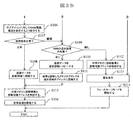
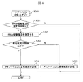
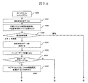
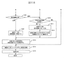
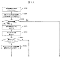
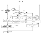
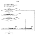
- FIG. 5 is a flowchart for explaining an example of a procedure in which a sub-microcomputer 120 diagnoses a drive current of a RAM 113 when the in-vehicle control device 100 starts up. It is a flowchart explaining an example of the procedure which the main microcomputer 110 diagnoses RAM113 when the vehicle-mounted control apparatus 100 shuts down. It is a flowchart following the flowchart of FIG. 5A. 10 is a flowchart for explaining an example of a procedure in which a sub-microcomputer 120 diagnoses a RAM 113 when the in-vehicle control device 100 shuts down.
- FIG. 5 is a flowchart for explaining an example of a procedure in which the main microcomputer 110 diagnoses a RAM 113 while the vehicle-mounted control device 100 is traveling in a vehicle. It is a flowchart following the flowchart of FIG. 7A. 5 is a flowchart for explaining an example of a procedure for the sub-microcomputer 120 to diagnose a RAM 113 while the vehicle-mounted control device 100 is traveling.
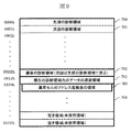
- 3 is an address diagram showing a storage area of a RAM 113.
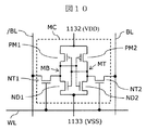
- FIG. 3 is a circuit diagram of a memory cell when a RAM 113 is a static random access memory (SRAM).
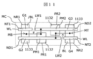
- FIG. FIG. 11 is a layout diagram of an example of the memory cell of FIG. 10.
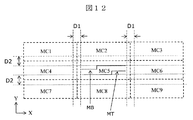
- FIG. 12 is a schematic diagram when the layout arrangement of the memory cells in FIG. 11 is arranged in a matrix. It is a typical block diagram of a static random access memory (SRAM).
- SRAM static random access memory
- an in-vehicle control device includes an arithmetic circuit (CPU) 111 that performs a control calculation for controlling a device, and a memory that temporarily stores data used by the arithmetic circuit. (Storage device, RAM) 113 and a current measurement circuit 150 capable of measuring a drive current supplied to the memory 113.
- the arithmetic circuit 111 diagnoses whether the memory 113 is normal based on the value of the drive current acquired from the current measurement circuit 150.
- the vehicle-mounted control device can capture a sign of failure before the memory 113 completely fails by providing the current measuring circuit 150.
- different bit values are written as check write data (hereinafter referred to as checker data) in adjacent memory cells of the memory 113.
- checker data check write data
- the drive current of the memory 113 is measured by the current measurement circuit 150.
- the measured value of the RAM drive current is compared with a preset determination threshold value, and the state of the memory 113 is diagnosed.
- a memory cell in which a driving current exceeding the determination threshold flows is regarded as a memory cell having a potential to become a failure in the future, although it has not completely failed.
- the address of a storage area including a memory cell having a potential to become a failure in the future is stored in an empty area (an unused storage area or an unused area) of the memory 113 before the memory cell completely fails. , The address of the storage area including the normal memory cell secured in advance is replaced.
- the vehicle-mounted control device it is possible to detect a failure of the memory 113 at an early stage, which can read and write data normally with respect to the memory 113 at the present time but may fail in the future. it can. Before a memory cell having a potential to become a failure in the future completely fails, the address of the storage area including the normal memory cell reserved in advance in the empty area of the memory 113 is the address of the storage area including the memory cell. Is replaced by Therefore, it is possible to prevent a failure of the memory 113 while the vehicle is traveling.
- the vehicle-mounted control process is continued by the vehicle-mounted control device according to the present invention. Therefore, the unit replacement of the in-vehicle control device due to the failure of the memory (RAM) 113 in the market, the number of returned products as complaints of the in-vehicle control device from customers, and the failure analysis of the in-vehicle control device are reduced. As a result, the reliability of the in-vehicle control device is improved.
- FIG. 1 is a configuration diagram of an in-vehicle control device 100 according to the present invention.
- the in-vehicle control device 100 is an in-vehicle electronic control device (ECU: Electronic Control Unit) that electronically controls in-vehicle devices (for example, an automatic transmission, an engine, etc.) mounted on the vehicle.
- the in-vehicle controller 100 includes a main microcomputer (hereinafter referred to as a main microcomputer) 110, a sub microcomputer (hereinafter referred to as a sub microcomputer) 120, a main power supply IC (Integrated Circuit) 130, a sub power supply IC 140, a current measurement circuit. 150 and an external memory 160.
- a main microcomputer hereinafter referred to as a main microcomputer
- a sub microcomputer hereinafter referred to as a sub microcomputer
- main power supply IC Integrated Circuit
- sub power supply IC 140 a current measurement circuit. 150 and an external memory 160.
- the main microcomputer 110 is a microcomputer (first microcomputer) that controls in-vehicle devices mounted on the vehicle.
- the main microcomputer 110 controls the in-vehicle device by controlling the actuator 230, for example.
- a message can be displayed via the display device 240.
- the message may be in any form, such as a message such as a character or an image, or a notification by lighting a lamp.
- the main microcomputer 110 includes a central processing unit (CPU) 111, a read only memory (ROM) 112, and a random access memory (RAM) 113.
- the CPU 111 is an arithmetic device (arithmetic circuit) that performs a control calculation necessary for controlling the in-vehicle device.
- the ROM 112 stores a program executed by the CPU 111 (for example, a diagnostic processing program described later with reference to FIGS. 3A to 8).
- the RAM 113 temporarily stores data used by the CPU 111.
- the sub-microcomputer 120 is a microcomputer (second microcomputer) having the same configuration as the main microcomputer 110, and the description thereof is omitted.
- the sub-microcomputer 120 can execute a process of diagnosing whether or not the RAM 113 is normal in accordance with a request or instruction from the main microcomputer 110 and notifying the main microcomputer 110 of the result of the diagnosis.
- the in-vehicle control device 100 receives power supply from a battery 220 mounted on the vehicle.
- a main power supply IC (main power supply circuit) 130 steps down or boosts or lowers the electric power VB received from the battery 220 and supplies it to the main microcomputer 110.
- the sub power supply IC (sub power supply circuit) 140 steps down or steps up / down the power received from the battery 220 and supplies it to the sub microcomputer 120.
- the main power supply IC 130 is internally divided into three power supply circuits so that power (power supplies) VB1, VB2, and VB3 can be individually supplied to the CPU 111, the ROM 112, and the RAM 113, respectively. That is, the main power supply IC 130 generates the first power supply circuit VG1 that generates the first power supply VB1 of the CPU 111, the second power supply circuit VG2 that generates the second power supply VB2 of the ROM 112, and the third power supply VB3 of the RAM 113.
- a power supply circuit VG3 is included. As will be described later, this is because the drive current supplied to the RAM 113 is suppressed from being affected by fluctuations in the drive current of the CPU 111 and the ROM 112.
- the first power supply VB1 generated from the first power supply circuit VG1 is supplied to the CPU 111 via the power supply wiring (power supply path) L1.
- the second power supply VB2 generated from the second power supply circuit VG2 is supplied to the ROM 112 via the power supply wiring (power supply path) L2.
- the third power supply VB3 generated from the third power supply circuit VG3 is supplied to the RAM 113 via the power supply wiring (power supply path) L3.
- the current measurement circuit 150 measures the value of the drive current supplied from the main power supply IC 130 to the RAM 113 and outputs the measurement result to the sub-microcomputer 120.
- the sub-microcomputer 120 diagnoses the RAM 113 by the procedure described later using the measurement result. The reason why the sub-microcomputer 120 performs diagnosis will be described later.
- the circuit configuration of the current measurement circuit 150 is not specifically described, those skilled in the art will readily understand that various circuit configurations are applicable.
- the measurement result may be output to the sub-microcomputer 120 as an analog signal or may be output to the sub-microcomputer 120 as a digital signal. When the measurement result is output as a digital signal, the current measurement circuit 150 is configured to include an analog / digital conversion circuit ADC.
- the sub-microcomputer 120 when outputting the measurement result as an analog signal, is configured to include an analog / digital conversion circuit ADC.
- ADC analog / digital conversion circuit
- the power signal 210 is generated accordingly.
- the in-vehicle control device 100 starts up / shuts down according to the power signal 210. Accordingly, the main power supply IC 130 and the sub power supply IC 140 supply power to or cut off the microcomputers 110 and 120.
- the external memory 160 is a storage device that is an electrically writable and erasable nonvolatile memory for storing a diagnosis result for the RAM 113, an address range targeted for diagnosis, and the like. As will be described later, the main microcomputer 110 / sub-microcomputer 120 diagnoses different storage areas of the RAM 113 when the in-vehicle control device 100 starts up or shuts down, or during steady processing after startup. Therefore, the address range to be diagnosed next time is stored in the external memory 160.
- the external memory 160 receives power from the main power supply IC 130 or the sub power supply IC 140.
- the external memory 160 is not particularly limited, but a non-volatile storage device such as a flash memory or an EEPROM can be used. Examples of the steady process include control and diagnosis of actuators such as an engine and a transmission, and fail-safe process performed by the in-vehicle control device 100.
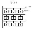
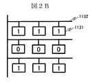
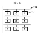
- FIG. 2A, 2B, and 2C show a state where checker data as diagnostic data is written to the memory cell of the RAM 113.
- FIG. In each figure, as memory cells of the RAM 113, nine memory cells 1131 arranged in an array of 3 rows and 3 columns are exemplarily shown.
- FIG. 2A is an example diagram schematically showing bit values stored in each memory cell when the checker data is written to the RAM 113.
- Each memory cell 1131 included in the RAM 113 is connected to a common power supply line 1132.
- the checker data is configured to store data having different bit values between the adjacent upper, lower, left, and right memory cells 1131. That is, in nine memory cells 1131 arranged in 3 rows and 3 columns as shown as an example, data of bit values of 1, 0 and 1 are stored in the three memory cells in the first row, respectively. .
- Three memory cells in the second row store data having bit values of 0, 1, and 0, respectively.
- Three memory cells in the third row store data of bit values of 1, 0, and 1, respectively.
- data of different bit values is stored between the adjacent upper, lower, left and right memory cells 1131. Since the memory cells 1131 generally represent bit values depending on the potential of the storage node (or high level “1”, low level “0”), different bit values are stored between the memory cells 1131. As a result, adjacent memory cells 1131 have different potentials.
- the sub-microcomputer 120 diagnoses an abnormality of the RAM 113 by using this fact in steps S203, S403, and S603. Even if data can be read / written normally from / to the memory cell 1131, the presence of such foreign matter may cause a short-circuit failure in the future. Therefore, in the present invention, the address of the storage area including the memory cell diagnosed as abnormal is the storage area including the normal memory cell reserved in the empty area (unused storage area or unused area) of the RAM 113 in advance. Is replaced with the address. As a result, it is possible to prevent malfunctions of actuators such as engines and transmissions that are contrary to the driver's intentions caused by the failure of the memory 113 while the vehicle is traveling, and unintended behaviors of the vehicle due to the malfunctions. is there.
- the checker data is selected as a data pattern that makes the leakage current manifest when a foreign object exists between the storage nodes of adjacent memory cells and is bridged.
- FIG. 2B is a diagram of another example schematically showing bit values stored in each memory cell when checker data is written to the RAM 113.
- data of bit values of 1, 1, 1 are stored in three memory cells in the first row.
- Bit values of 0, 0, and 0 are stored in the three memory cells in the second row.
- the three memory cells in the third row store data having bit values of 1, 1, 1.
- the checker data is configured to store data having different bit values between the upper and lower memory cells.
- the three memory cells 1131 in the second row and the three memory cells 1131 in the first and third rows are configured to store data of different bit values.
- This checker data is effective, for example, in detecting a leakage current due to a short circuit between storage nodes of memory cells arranged above and below.
- FIG. 2C is a diagram of another example schematically showing bit values stored in each memory cell when the checker data is written to the RAM 113.
- nine memory cells 1131 data of bit values of 1, 0, 1 are stored in three memory cells in the first row.
- Three memory cells in the second row store data with bit values of 1, 0, and 1.
- Three memory cells in the third row store data with bit values of 1, 0, and 1.
- the checker data is configured to store data having different bit values between the left and right memory cells. That is, three memory cells 1131 in the second column and three memory cells 1131 in the first and third columns are configured to store data having different bit values.
- This checker data is effective, for example, in detecting a leakage current due to a short circuit between storage nodes of memory cells arranged on the left and right.
- the data pattern configuration of the checker data depends on the layout configuration of the memory cells and the layout configuration of a plurality of memory cells arranged in an array. More specifically, since it depends on the layout configuration of the storage nodes of the memory cells and the arrangement and distance of the storage nodes between the memory cells, the layout configuration of the memory cells and the layout of the plurality of memory cells employed in the RAM 113 to be diagnosed It is good to select in consideration of the configuration.
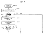
- FIG. 3A and FIG. 3B are examples of a flowchart for explaining a procedure for the main microcomputer 110 to diagnose the RAM 113 when the in-vehicle control device 100 starts up.
- the parts 1, 2, 3 shown in FIG. 3A are connected to the parts 1, 2, 3 shown in FIG. 3B, respectively.
- Step S100 When the main microcomputer 110 receives the power signal 210 indicating that the power is turned on, the main microcomputer 110 starts this flowchart. It is assumed that the main power supply IC 130 and the sub power supply IC 140 have already started supplying power according to the power supply signal 210 at the time of starting this flowchart.
- Step S101 The main microcomputer 110 reads from the external memory 160 the previous diagnosis result for the RAM 113 and the address of the storage area on the RAM 113 to be diagnosed this time.
- Step S102 If it is determined that a failure has occurred in the previous diagnosis of the RAM 113, the process skips to step S112. If normal or not diagnosed, the process proceeds to step S103.
- the previous diagnosis result referred to here is, for example, a diagnosis result at the previous shutdown when the diagnosis of the RAM 113 is performed at startup, at shutdown, and during traveling, as will be described later. If the RAM 113 had a failure at the time of the previous shutdown, it is considered that the RAM 113 has also failed this time, so in this case, the process skips to step S112.
- Step S103 The main microcomputer 110 saves the data stored in the storage area of the diagnosis target address read out in step S101 in a save area prepared for saving in advance.
- checker data is data configured such that adjacent memory cells have different potentials by storing different bit values.
- Step S105 The main microcomputer 110 reads data from the address where the checker data is written. If the read data matches the written checker data, the process proceeds to step S105, and if not, the process proceeds to step S108.
- the main microcomputer 110 instructs the sub microcomputer 120 to measure the drive current of the RAM 113.
- the sub-microcomputer 120 measures the drive current according to a flowchart described later with reference to FIG. 4 and notifies the main microcomputer 110 of the measurement result.
- Step S107 The main microcomputer 110 receives the drive current measurement result from the sub-microcomputer 120. If the measurement result is normal, the process proceeds to step S108. If the measurement result is abnormal, the process proceeds to step S109.
- Step S108 If the measurement result is normal, the data saved in step S103 is written back to the current diagnosis area.
- Step S109 The main microcomputer 110 confirms the presence or absence of an empty area (unused area) in the RAM 113 prepared in advance as a storage area after replacement of the memory cell determined to be faulty. If there is a free area in the RAM 113, the process proceeds to step S110. If there is no free area in the RAM 113, the process proceeds to step S112.
- An empty area (unused area) means a storage area of a part where data used by the CPU 111 is not stored.
- Step S110 The main microcomputer 110 copies the data saved in S103 to an empty area.
- Step S111 The main microcomputer 110 replaces the address of the memory diagnosed as a failure with the address of a normal memory secured in advance in the free space of the RAM 113.
- the main microcomputer 110 stores the diagnosis result of the RAM 113 and the next diagnosis target address in the external memory 160.
- Step S113 The main microcomputer 110 displays a message on the display device 240 that the diagnosis result of the RAM 113 is a failure.
- the main microcomputer 110 starts the fail safe mode.
- the fail safe mode is a mode in which the operation is performed by degenerating the function and defeating it to the safe side.
- the main microcomputer 110 disables the vehicle control based on the driver's steering instruction and prevents the actuator 230 from being in a safe driving mode in order to prevent erroneous control of the vehicle due to the failure of the RAM 113. Control.
- the main microcomputer 110 stores the diagnosis result of the RAM 113 and the next diagnosis target address in the external memory 160.
- Step S116 The main microcomputer 110 starts a steady process of the in-vehicle control device 100.
- FIG. 4 is an example of a flowchart illustrating a procedure in which the sub-microcomputer 120 diagnoses the drive current of the RAM 113 when the in-vehicle control device 100 starts up.
- the sub-microcomputer 120 diagnoses the drive current of the RAM 113 when the in-vehicle control device 100 starts up.
- Step S200 When the sub-microcomputer 120 receives the power signal 210 indicating that the power is turned on, the sub-microcomputer 120 starts this flowchart. It is assumed that the main power supply IC 130 and the sub power supply IC 140 have already started supplying power according to the power supply signal 210 at the time of starting this flowchart.
- Step S201 The sub-microcomputer 120 determines whether or not an instruction for instructing to measure the driving current of the RAM 113 is received from the main microcomputer 110. When there is an instruction, the process proceeds to step S202, and when there is no instruction, this flowchart is ended (END).
- Step S202 The sub microcomputer 120 acquires the drive current value of the RAM 113 from the current measurement circuit 150.
- Step S203 The sub-microcomputer 120 determines whether or not the acquired drive current value is equal to or less than a determination threshold value. If the acquired drive current value is lower than the determination threshold, it is determined that the RAM 113 is normal, and the process proceeds to step S204. If the acquired drive current value is higher than the determination threshold, it is determined that there is a failure and the process proceeds to step S205.
- the determination threshold value can be stored in advance in a non-volatile memory such as a ROM provided in the sub microcomputer 120 (or the main microcomputer 110).
- Step S203 Supplement
- the main power supply IC 130 is configured to individually supply power to these circuit components.
- the sub-microcomputer 120 transmits a diagnosis result indicating that the drive current of the RAM 113 is normal to the main microcomputer 110 (S204).
- the sub-microcomputer 120 transmits a diagnosis result indicating that the drive current of the RAM 113 is abnormal to the main microcomputer 110 (S205).
- FIG. 5A and FIG. 5B are examples of a flowchart for explaining a procedure in which the main microcomputer 110 diagnoses the RAM 113 when the in-vehicle control device 100 shuts down.
- FIG. 5A and FIG. 5B each step of FIG. 5A and FIG. 5B will be described. Note that the portions 4, 5, and 6 shown in FIG. 5A are connected to the portions 4, 5, and 6 shown in FIG. 5B, respectively.
- FIG. 5A Steps S300 to S301
- the main microcomputer 110 receives the power signal 210 indicating that the power has been cut off
- the main microcomputer 110 starts this flowchart (S300).
- the main microcomputer 110 ends the steady process of the in-vehicle control device 100 (S301).
- Steps S302 to S308 are the same as steps S101 to S108 in FIGS. 3A and 3B. However, if the previous diagnosis result is abnormal in step S303, the process proceeds to step S314 in FIG. 5B.
- Step S310 The main microcomputer 110 confirms the presence or absence of an empty area in the RAM 113 prepared in advance as an area after replacement of the memory cell determined to be faulty. If there is a free area in the RAM 113, the process proceeds to S311. If there is no free area in the RAM 113, the process proceeds to S313.
- Steps S311 to S312 Steps S311 to S312 are the same as steps S110 to S111 in FIG. 3B.
- Step S313 is the same as step S115 of FIG. 3B.
- FIG. 5B Steps S314 to S315.
- the main microcomputer 110 transmits a shutdown signal to the main power supply IC 130 and the sub power supply IC 140 (S314).
- the power supply ICs stop power supply, and the main microcomputer 110 and the sub-microcomputer 120 are turned off (S315).
- step S309 is executed in which the saved data is written back to the current diagnosis area. Thereby, the flowcharts of FIGS. 3A and 3B are executed again.
- FIG. 6 is a flowchart illustrating a procedure for the sub-microcomputer 120 to diagnose the RAM 113 when the in-vehicle control device 100 shuts down. It is assumed that the main power supply IC 130 and the sub power supply IC 140 are continuously supplying power at the time of starting this flowchart. Hereinafter, each step of FIG. 6 will be described. When the vehicle-mounted control apparatus 100 shuts down, the process proceeds to step S400 in the flowchart.
- Steps S401 to S405 are the same as steps S201 to S205 in FIG.
- Step S406 The sub microcomputer 120 is turned off because the main microcomputer 110 sends a shutdown signal to the sub power IC in step S315.
- FIGS. 7A and 7B are flowcharts for explaining a procedure in which the main microcomputer 110 diagnoses the RAM 113 while the in-vehicle control device 100 is performing a scheduled process.
- the control, diagnosis, communication, and the like of the actuators such as the engine and the transmission are divided into a plurality of tasks by the in-vehicle control device 100 and executed at regular intervals.
- the task for diagnosing the RAM 113 of the present invention shown in FIGS. 7A and 7B is executed as a part of the routine process.
- each step of FIG. 7A and FIG. 7B is demonstrated. Note that the portions 7, 8, and 9 shown in FIG. 7A are connected to the portions 7, 8, and 9 shown in FIG. 7B, respectively.
- FIG. 7A Step S500
- the main microcomputer 110 receives the power signal 210 indicating that the power is turned on, completes the start-up process of FIGS. 3A and 3B, shifts to a steady process, and then starts this flowchart.
- Steps S501 to S515 are the same as steps S101 to S115 in FIGS. 3A and 3B.
- FIG. 8 is an example of a flowchart for explaining a procedure in which the sub-microcomputer 120 diagnoses the RAM 113 while the in-vehicle control device 100 is performing a scheduled process. Hereinafter, each step of FIG. 8 will be described.
- Step S600 The sub-microcomputer 120 receives the power signal 210 indicating that the power is turned on, completes the start-up process of FIGS. 3A and 3B, shifts to a steady process, and then starts this flowchart.
- Steps S601 to S605 are the same as steps S201 to S205 in FIG.
- FIG. 9 is an example of an address diagram showing a storage area of the RAM 113. If it is attempted to diagnose all the storage areas of the RAM 113 at once, it takes a long time to diagnose. In addition, it is necessary to determine the failure area on the memory cell. Therefore, as shown in FIG. 9, the entire storage area of the RAM 113 is divided into a plurality of diagnosis areas by dividing the diagnosis target address into a plurality of parts. Then, as described with reference to FIGS. 3A to 8, the storage areas at different addresses are diagnosed as diagnosis areas in one or both of startup, shutdown, and steady state processing.
- the main microcomputer 110 / sub-microcomputer 120 writes the next diagnosis target address to the external memory 160 each time diagnosis is performed, and determines the diagnosis target address according to this in the next diagnosis.
- the diagnosis area 700 to 702 of the memory address 0000h-FFEEh (the h at the end indicates a hexadecimal address) is composed of the first diagnosis area 700, the next diagnosis area 701, and the last diagnosis area 702.
- the process returns to the first diagnosis area 700.
- a data save area 703 in the diagnosis area is secured at the memory address FFEFh.
- Memory addresses FFF0h to FFFFh are secured as free areas (unused areas) 704.
- a storage area 705 after replacement of the storage area diagnosed as a failure is secured in a free area (unused area) 704.
- the main microcomputer 110 displays a message on the display device 240 that the diagnosis result of the RAM 113 is a failure, and starts the fail-safe mode.
- the allocation of the memory address area described above is an example, and is not limited thereto, and may be changed as appropriate.
- FIG. 10 shows a circuit diagram of the memory cell MC in the case where the RAM 113 is a static random access memory (SRAM: Static Random Access Memory).
- the memory cell MC is a CMOS type 6 transistor and includes the following.
- Memory cell MC includes P channel MOS transistors PM1, PM2 and N channel MOS transistors NT1, NT2, ND1, ND2.
- the source / drain paths of the P-channel MOS transistors PM1 and PM2, which are load transistors, are connected between the power supply potential (VDD) 1132 line and the first and second storage nodes MB and MT, respectively, and their gates are Respectively connected to the second and first storage nodes MT, MB.
- the source / drain paths of the N-channel MOS transistors ND1 and ND2 which are driving transistors are connected between the first and second storage nodes MB and MT and the ground potential (VSS) 1133 line, respectively, and their gates are Respectively connected to the second and first storage nodes MT, MB.
- Source / drain paths of N-channel MOS transistors NT1 and NT2 serving as transfer transistors are connected between storage nodes MB and MT and bit lines / BL and BL, respectively, and their gates are both connected to a word line WL.
- the MOS transistors PM1 and ND1 form an inverter that provides an inverted signal of the signal of second storage node MT to first storage node MB.
- MOS transistors PM2 and ND2 form an inverter that provides an inverted signal of the signal of second storage node MB to first storage node MT.
- the two inverters are connected in antiparallel between the first and second storage nodes MB and MT, and constitute a latch circuit.
- the N-channel MOS transistors NT1 and NT2 become conductive.
- one bit line (for example, BL) of bit line pair BL, / BL is set to "H” level and the other bit line (/ BL in this case) is set to "L” level.
- MOS transistors PM2 and ND1 are turned on and MOS transistors PM1 and ND2 are turned off, so that the levels of storage nodes MB and MT are latched.
- word line WL is set to the “L” level, which is a non-selection level, N channel MOS transistors NT1 and NT2 are rendered non-conductive, and a data signal is stored in memory cell MC.
- bit line pair BL, / BL is precharged to “H” level, and then the word line WL is set to “H” level of the selection level.
- a current flows from the bit line (in this case, / BL) to the ground potential GND line via the N-channel MOS transistors NT1, NT2, and the potential of the bit line / BL decreases.
- the memory cell MC When the memory cell MC stores high level data “1”, the levels of the first and second storage nodes MB and MT are set to “0” and “1”, respectively. When the memory cell MC stores low level data “0”, the levels of the first and second storage nodes MB and MT are set to “1” and “0”, respectively.
- a plurality of memory cells MC are provided in a matrix.
- the lines of the power supply potential (VDD) 1132 of the plurality of memory cells MC are coupled in common.
- the coupled line of power supply potential (VDD) 1132 is coupled to the current measurement circuit 150 shown in FIG.
- FIG. 13 shows an example in which the drive current of the RAM 113 is measured by the current measurement circuit 150, the current consumption value of the RAM 113 may be measured instead.
- the current measurement circuit 150 is provided in the line of the ground potential (VSS) 1133.
- the drive current and consumption current of the RAM 113 may be rephrased as the operation current of the RAM 113.
- FIG. 11 is an example of a schematic layout diagram of the memory cell MC shown in FIG. It includes gate electrodes G1, G2, G3, G4 such as polysilicon.
- Gate electrode G1 serves as the gate of N-channel MOS transistor NT1, and is coupled to word line WL.
- Gate electrode G2 serves as the gate of N-channel MOS transistor ND1 and P-channel MOS transistor PM1.
- Gate electrode G3 serves as the gate of N-channel MOS transistor ND2 and P-channel MOS transistor PM2.
- Gate electrode G4 serves as the gate of N-channel MOS transistor NT2, and is coupled to word line WL.
- N-type region NR1 is formed using gate electrodes G1 and G2 as an impurity introduction mask, and N-channel MOS transistors NT1 and ND1 are formed.
- N-type region NR2 is formed using gate electrodes G4 and G3 as an impurity introduction mask, and N-channel MOS transistors NT2 and ND2 are formed.
- P-type region PR1 is formed using gate electrode G2 as an impurity introduction mask, and P-channel MOS transistor PM1 is formed.
- P-type region PR2 is formed using gate electrode G3 as an impurity introduction mask, and P-channel MOS transistor PM2 is formed. In FIG.
- bit line / BL is coupled to N-type region NR1 (the source of N-channel MOS transistor ND1) formed above gate electrode G1.
- bit line / BL is coupled to N-type region NR1 (the source or drain of N-channel MOS transistor NT1) formed above gate electrode G1.
- bit line BL is coupled to N-type region NR2 (the source or drain of N-channel MOS transistor NT2) formed below gate electrode G4.
- the line of the power supply potential (VDD) 1132 corresponds to a P-type region PR1 (source of PM1) formed below the gate G2 and a P-type region PR2 (source of PM2) formed above the gate G3.
- the line of the ground potential (VSS) 1133 corresponds to the N-type region NR1 (the source of the N-channel MOS transistor ND1) formed below the gate G2 and the N-type region NR2 (the source of the N-channel MOS transistor ND1). Coupled to the source of N-channel MOS transistor ND2.
- the first storage node MB includes an N-type region NR1 (the drain of the N-channel MOS transistor ND1) between the gate electrodes G1 and G2, a P-type region PR1 on the drain side of the P-channel MOS transistor PM1, and a gate electrode G3.
- the second storage node MT includes an N-type region NR2 (the drain of the N-channel MOS transistor ND2) between the gate electrodes G3 and G4, a P-type region PR2 on the drain side of the P-channel MOS transistor PM2, and a gate electrode G2.
- LW2 the drain of the N-channel MOS transistor ND1
- FIG. 12 is a schematic diagram when the layout arrangement of the memory cells in FIG. 11 is arranged in a matrix.
- the memory cells MC1 to MC9 shown as examples are arranged in a matrix.
- the memory cell MC5 schematically shows the first and second storage nodes MB and MT of FIG.
- the storage nodes of other memory cells are omitted because the drawing becomes complicated.
- a mirror-symmetrical arrangement, a line-symmetrical arrangement, or a repeated arrangement can be adopted as the layout arrangement of the memory cells MC1 to MC9.
- the distance D ⁇ b> 1 indicates the storage node interval between the left and right adjacent memory cells in the horizontal direction (X direction).
- the distance D2 indicates the interval between the storage nodes between the upper and lower adjacent memory cells in the vertical direction (Y direction).
- the RAM 113 is a static random access memory (SRAM)
- the memory cells MC1 to MC9 are formed according to the minimum processing size of the semiconductor manufacturing process. Accordingly, the distances D1 and D2 are extremely narrow.
- the storage node between adjacent memory cells is caused by the foreign matter.
- the checker data is appropriately selected from the checker data described in FIGS. 2A, 2B, and 2C in consideration of the layout configuration of the storage nodes of the memory cells, the arrangement of the storage nodes between the memory cells, and their distances. Selection or a combination thereof can be used.
- FIG. 13 is a schematic block diagram when the RAM 113 is a static random access memory (SRAM).
- a plurality of memory cells MC are arranged in a matrix to form a memory cell array MA.
- the first word line (WL0) is coupled to the memory cell arranged in the first row
- the second word line (WL1) is connected to the memory cell arranged in the second row.
- the third word line (WL2) is coupled to the memory cell arranged in the third row.
- a fourth word line (WL3), a fifth word line (WL4), a sixth word line (WL5), and a seventh word line (WL6) to an n ⁇ 1th word line (WLn) are provided.
- a first bit line pair (/ BL0, BL0) is coupled to the memory cell arranged in the first column.
- a second bit line pair (/ BL1, BL1) is coupled to the memory cell arranged in the second column.
- the third bit line pair (/ BL2, BL2) to the (n-1) th bit line pair (/ BLn, BLn) are provided.
- the number of word lines and the number of bit line pairs described above are examples.
- the row selection circuit RDEC selects one word line corresponding to the row address signal among the plurality of word lines (WL0 to WLn) in accordance with the row address signal supplied from the CPU 111.
- the column selection circuit CDEC selects one or more bit line pairs corresponding to the row address signal from the plurality of bit line pairs (/ BL0, BL0 ⁇ / BLn, BLn) according to the column address signal supplied from the CPU 111. To do.
- the input / output control circuit IOCKT reads data from one or more memory cells coupled to the selected word line and the selected one or more bit line pairs, and the read data is read out. It supplies to CPU111.
- the input / output control circuit IOCKT writes the data supplied from the CPU 111 to one or more memory cells coupled to the selected word line and the selected one or more bit line pairs. .
- the diagnosis area is set based on the address of the RAM 113.
- the diagnosis area may be set according to the number of word lines in the RAM 113, although not particularly limited. That is, a plurality of continuous addresses for selecting a plurality of memory cells connected to one word line may be set as one diagnostic area.
- a plurality of memory cells connected to a plurality of word lines for example, three consecutive word lines can be set as one diagnostic region. In this case, the checker data shown in FIG. 2A (or FIG. 2B, FIG. 2C) is written, and the diagnosis is executed.
- FIG. 2A or FIG. 2B, FIG. 2C
- the three consecutive word lines mean three word lines in which the first word line WL0, the second word line WL1, and the third word line WL2 are continuous, and the fourth word line WL3, It means three word lines in which the fifth word line WL4 and the sixth word line WL5 are continuous.
- a plurality of memory cells connected to the first word line WL0, the second word line WL1, and the third word line WL2 are included in one diagnostic region R1.
- a plurality of memory cells in which the fourth word line WL3, the fifth word line WL4, and the sixth word line WL5 are connected to three word lines are included in one diagnostic region R2.
- the diagnosis area R1 and the diagnosis area R2 are assigned by a plurality of continuous addresses.
- the next diagnostic region r2 May be set as the third word line WL2, the fourth word line WL3, and the fifth word line WL4. That is, an overlapping portion (memory cell connected to the third word line WL2) is provided in two consecutive diagnostic regions r1 and r2. In this case, a diagnosis can be made between the storage node of the memory cell coupled to the third word line and the storage node of the memory cell coupled to the fourth word line.
- the current measurement circuit 150 in FIG. 1 is coupled to the power supply wiring (L31), and measures the drive current (operating current) flowing through the power supply wiring (L31).
- the in-vehicle control device 100 can catch a sign of failure before the memory (RAM) 113 completely fails.
- different bit values are written as check write data (checker data) in adjacent memory cells 1131 of the memory (RAM) 113.
- the drive current of the memory (RAM) 113 is measured by the current measurement circuit 150 in a state where the checker data is written to the memory (RAM) 113.
- the state of the memory (RAM) 113 is diagnosed based on whether or not the measured drive current value exceeds a threshold value.
Landscapes
- Engineering & Computer Science (AREA)
- Theoretical Computer Science (AREA)
- General Engineering & Computer Science (AREA)
- Physics & Mathematics (AREA)
- General Physics & Mathematics (AREA)
- Computer Hardware Design (AREA)
- Quality & Reliability (AREA)
- For Increasing The Reliability Of Semiconductor Memories (AREA)
- Techniques For Improving Reliability Of Storages (AREA)
- Test And Diagnosis Of Digital Computers (AREA)
Abstract
Description
(故障その1)メモリセルの値が「0」または「1」に固定される縮退故障。
(故障その2)あるメモリセルが格納している値が変化するのと連動して他のメモリセルの値も変化するカプリング故障。
(故障その3)メモリアドレスを正しく選択できないアドレスデコーダ故障。
(故障その4)あるメモリセルに隣接する上下左右に配置されたメモリセルが記憶している値の影響を受けて、当該メモリセルが記憶している値も変化する、パターンセンシティブ故障。
このチェッカーデータは、上下のメモリセル間で異なるビット値のデータを格納するように構成されている。すなわち、2行目の3個のメモリセル1131と、1行目および3行目のそれぞれ3個のメモリセル1131とで、異なるビット値のデータを格納するように構成されている。このチェッカーデータは、例えば、上下に配置されたメモリセルの記憶ノード間の短絡によるリーク電流の検出に有効である。
2行目の3個のメモリセルには、1、0、1のビット値のデータが格納される。3行目の3個のメモリセルには、1、0、1のビット値のデータが格納される。このチェッカーデータは、左右のメモリセル間で異なるビット値のデータを格納するように構成されている。すなわち、2列目の3個のメモリセル1131と、1列目および3列目のそれぞれ3個のメモリセル1131とで、異なるビット値のデータを格納するように構成されている。
このチェッカーデータは、例えば、左右に配置されたメモリセルの記憶ノード間の短絡によるリーク電流の検出に有効である。
メインマイコン110は、電源が投入されたことを示す電源信号210を受信すると、本フローチャートを開始する。本フローチャートを開始する時点において、メイン電源IC130とサブ電源IC140はそれぞれ電源信号210にしたがって電力供給を開始済であるものとする。
メインマイコン110は、外部メモリ160から前回実施したRAM113に対する診断結果と、今回診断するRAM113上の記憶領域のアドレスを読み出す。
前回実施したRAM113に対する診断により故障と判定された場合は、ステップS112へスキップする。正常または診断未実施である場合は、ステップS103へ進む。ここでいう前回診断結果とは、例えば、後述するようにスタートアップ時とシャットダウン時と走行中各々においてRAM113の診断を実施する場合は、前回シャットダウン時における診断結果である。前回シャットダウン時においてRAM113が故障であったのであれば、今回スタートアップ時も故障であると考えられるので、かかる場合はステップS112へスキップすることとした。
メインマイコン110は、ステップS101で読み出した診断対象アドレスの記憶領域に格納されたデータを、あらかじめ退避用に用意した退避領域に退避する。
メインマイコン110は、ステップS101で読み出した診断対象アドレスに対して、診断用データとされるチェッカーデータを書き込む。図2A、図2B、図2Cで説明したように、チェッカーデータは隣接するメモリセルが互いに異なるビット値を格納することにより互いに異電位となるように構成されたデータである。
メインマイコン110は、チェッカーデータを書き込んだアドレスからデータを読み出す。読み出したデータと書き込んだチェッカーデータが一致する場合はステップS105へ進み、一致しない場合はステップS108へ進む。
メインマイコン110は、サブマイコン120に対して、RAM113の駆動電流を測定するよう指示する。サブマイコン120は、後述の図4で説明するフローチャートにしたがって駆動電流を測定し、その測定結果をメインマイコン110に対して通知する。
メインマイコン110は、サブマイコン120から駆動電流の測定結果を受け取る。測定結果が正常である場合はステップS108へ進み、異常である場合はステップS109へ進む。
測定結果が正常である場合、ステップS103で退避したデータが、現在の診断領域へ書き戻される。
メインマイコン110は、故障と判断したメモリセルの置換後の記憶領域として、あらかじめ用意している、RAM113の空き領域(未使用領域)の有無を確認する。RAM113の空き領域が有る場合、ステップS110に進み、RAM113の空き領域が無い場合は、ステップS112に進む。空き領域(未使用領域)とは、CPU111により利用さるデータが格納されていない部分の記憶領域を意味する。
メインマイコン110は、S103で退避したデータを空き領域にコピーする。
メインマイコン110は、故障と診断したメモリのアドレスをあらかじめRAM113の空き領域に確保している正常なメモリのアドレスに置換する。
メインマイコン110は、外部メモリ160にRAM113の診断結果と次回の診断対象アドレスを格納する。
メインマイコン110は、RAM113の診断結果が故障であった旨のメッセージを表示装置240上に表示する。
メインマイコン110は、フェールセーフモードを開始する。フェールセーフモードとは、機能を縮退して安全側に倒した動作を実施するモードである。メインマイコン110は、フェールセーフモードにおいては、RAM113の故障により車両を誤制御することを防止するため、運転者の操縦指示に基づいた自動車制御を無効とし、安全な走行モードとなるようにアクチュエータ230を制御する。
メインマイコン110は、外部メモリ160にRAM113の診断結果と次回の診断対象アドレスを格納する。
メインマイコン110は、車載制御装置100の定常処理を開始する。
サブマイコン120は、電源が投入されたことを示す電源信号210を受信すると、本フローチャートを開始する。本フローチャートを開始する時点において、メイン電源IC130とサブ電源IC140はそれぞれ電源信号210にしたがって電力供給を開始済であるものとする。
サブマイコン120は、メインマイコン110からRAM113の駆動電流を測定するよう指示する命令を受け取っているか否かを判定する。指示が有る場合はステップS202へ進み、無い場合は本フローチャートを終了(END)する。
サブマイコン120は、電流測定回路150から、RAM113の駆動電流値を取得する。
サブマイコン120は、取得した駆動電流値が判定閾値以下であるか否かを判定する。
取得した駆動電流値が判定閾値を下回る場合はRAM113が正常であると判断してステップS204へ進み、取得した駆動電流値が判定閾値を上回る場合は故障であると判断してステップS205へ進む。判定閾値は、サブマイコン120(または、メインマイコン110)が備えるROMなど不揮発性メモリにあらかじめ格納しておくことができる。
本ステップにおいては駆動電流値と判定閾値を比較しているので、駆動電流を正確に取得することが必要である。CPU111、ROM112などのRAM113以外の他回路部品に対して電力を供給する電源パスと、RAM113に対して電力を供給する電源パスとが共通になっていると、他回路部品の電圧や電流の影響を受けてRAM113の駆動電流が変動し、正確な値を取得できない可能性がある。そのため、図1で説明されたように、メイン電源IC130は、これら回路部品に対してそれぞれ個別に電力を提供するように、構成されている。
サブマイコン120は、メインマイコン110に対して、RAM113の駆動電流が正常である旨の診断結果を送信する(S204)。サブマイコン120は、メインマイコン110に対して、RAM113の駆動電流が異常である旨の診断結果を送信する(S205)。
メインマイコン110は、電源が遮断されたことを示す電源信号210を受信すると、本フローチャートを開始する(S300)。メインマイコン110は、車載制御装置100の定常処理を終了する(S301)。
ステップS302~S308は、図3Aおよび図3BのステップS101~S108と同様である。ただし、ステップS303において、先回診断結果が異常である場合には、図5BのステップS314に移行する。
メインマイコン110は、故障と判断したメモリセルの置換後の領域とてあらかじめ用意している、RAM113の空き領域の有無を確認する。RAM113の空き領域が有る場合は、S311に進み、RAM113の空き領域が無い場合は、S313に進む。
ステップS311~S312は、図3BのステップS110~S111と同様である。
ステップS313は、図3BのステップS115と同様である。
メインマイコン110は、メイン電源IC130とサブ電源IC140に対してシャットダウン信号を送信する(S314)。これにより各電源ICは電力供給を停止するので、メインマイコン110、サブマイコン120はOFFになる(S315)。
ステップS401~S405は、図4のステップS201~S205と同様である。
サブマイコン120は、メインマイコン110により、ステップS315でサブ電源ICへシャットダウン信号が送られるため、電源OFFとなる。
メインマイコン110は、電源が投入されたことを示す電源信号210を受信し、図3Aおよび図3Bのスタートアップ処理を完了し、定常処理に移行した後、本フローチャートを開始する。
ステップS501~S515は、図3Aおよび図3BのステップS101~S115と同様である。
サブマイコン120は、電源が投入されたことを示す電源信号210を受信し、図3Aおよび図3Bのスタートアップ処理を完了し、定常処理に移行した後、本フローチャートを開始する。
ステップS601~S605は、図4のステップS201~S205と同様である。
本発明に係る車載制御装置100は、前記電流測定回路150を設けることにより、メモリ(RAM)113が完全に故障する前に、故障の予兆を捉えることが可能である。故障の予兆を捉えるため、メモリ(RAM)113の隣接するメモリセル1131に対し、例えば、互いに異なるビット値がチェック用の書込みデータ(チェッカーデータ)として書き込まれる。チェッカーデータがメモリ(RAM)113に対して書き込まれた状態で、メモリ(RAM)113の駆動電流が前記電流測定回路150により測定される。測定された駆動電流の値が閾値を超えているか否かに基づき、メモリ(RAM)113の状態が診断される。これにより、現時点では正常にデータを読み書きできるが将来的に故障を生じさせる可能性のあるメモリセル1131間の異物を早期の段階で検出することができる。将来的に故障を生じさせる可能性のあるメモリセルが完全に故障する前に、そのメモリセルを含む記憶領域のアドレスが、メモリ(RAM)113の空き領域にあらかじめ確保された正常なメモリセルを含む記憶領域のアドレスへと置換される。そのため、車両走行中におけるメモリ(RAM)113の故障を未然に防ぐことができる。したがって、車両走行中に、メモリ(RAM)113の故障が原因により発生するドライバーの意図に反したエンジンやトランスミッション等のアクチュエータの誤動作、および、その誤動作に起因する車両の意図しない挙動を防ぐことが可能である。車両走行中に、RAMが故障し、フェールセーフ処理に移行する制御が行われ、運転性能が低下することを可能な限り防ぐことができる。
Claims (10)
- 車両が搭載している機器を制御する車載制御装置であって、
前記機器を制御するための制御演算を実施可能な演算回路、
前記演算回路が使用するデータを一時的に記憶可能な記憶装置、
前記記憶装置に対して供給される駆動電流の値を測定可能な電流測定回路、
を備え、
前記演算回路は、前記電流測定回路から取得した前記駆動電流の値に基づき前記記憶装置が正常であるか否かを診断する、
ことを特徴とする車載制御装置。 - 前記演算回路は、前記記憶装置の隣接するメモリセルに対して互いに異なるビット値を書き込むことにより、前記隣接するメモリセルが互いに異なる電位となるようにした状態で、前記診断を実施する、
ことを特徴とする請求項1記載の車載制御装置。 - 前記演算回路は、前記電流測定回路から取得した前記駆動電流の値が判定閾値を超えているか否かに基づき前記記憶装置が正常であるか否かを診断する
ことを特徴とする請求項1記載の車載制御装置。 - 前記演算回路は、前記記憶装置の診断領域を故障と判断した場合、前記記憶装置の診断領域に格納されたデータを、あらかじめ用意した前記記憶装置の空き領域に格納し、前記記憶装置の診断領域のアドレスを、前記記憶装置の空き領域のアドレスへ置換する、
ことを特徴とする請求項1記載の車載制御装置。 - 警告メッセージを表示する表示装置を備え、
前記演算回路は、前記診断により前記記憶装置を故障と判断し、あらかじめ用意した前記記憶装置の空き領域が故障セルのデータで置換済みの場合、前記記憶装置が故障である旨の警告メッセージを前記表示装置に表示させるとともに、所定のフェールセーフ処理を実施する、
ことを特徴とする請求項1記載の車載制御装置。 - 前記車載制御装置は、前記記憶装置に対してのみ電力を供給する電源回路を備え、
前記電流測定回路は、前記電源回路が前記記憶装置に対して供給する前記駆動電流を測定する、
ことを特徴とする請求項1記載の車載制御装置。 - CPU、RAMを含む第1マイクロコンピュータと、
前記CPUへ第1電源を供給するための第1電源配線と、
前記RAMへ第2電源を供給するための第2電源配線と、
前記第1電源配線に結合された第1電源回路と、
前記第2電源配線に結合された第2電源回路と、
前記第2電源配線に結合され、前記RAMの駆動電流の値を測定可能な電流測定回路と、
前記電流測定回路に結合された第2マイクロコンピュータと、
を含み、
前記第2マイクロコンピュータは、前記電流測定回路から取得した前記駆動電流の値に基づき前記RAMが正常であるか異常であるかを診断し、診断結果を前記CPUへ送付する車載制御装置。 - 不揮発性メモリを、さらに、含み、
前記RAMは、アドレスによって判別され、それぞれが診断対象とされる複数の記憶領域を含み、
前記CPUは、前記不揮発性メモリへ前記診断結果と次回に診断対象とされるべき記憶領域のアドレスとを格納する、
ことを特徴とする請求項7記載の車載制御装置。 - 前記CPUは、前記診断に際し、前記診断対象とされるべき記憶領域内に格納されたデータを前記RAMに設けられた退避領域へ格納した後、前記診断対象とされるべき記憶領域へ診断用データの書き込みを行い、前記診断用データが前記診断対象とされるべき記憶領域に書き込まれた状態で、前記第2マイクロコンピュータへ前記電流測定回路による前記RAMの前記駆動電流の値の測定を指示する、
ことを特徴とする請求項8記載の車載制御装置。 - 前記診断用データは、前記RAMの隣接するメモリセルに互いに異なるビット値を設定する、
ことを特徴とする請求項9記載の車載制御装置。
Priority Applications (3)
| Application Number | Priority Date | Filing Date | Title |
|---|---|---|---|
| JP2018547211A JP6694517B2 (ja) | 2016-10-26 | 2017-09-27 | 車載制御装置 |
| CN201780062622.9A CN109844724B (zh) | 2016-10-26 | 2017-09-27 | 车载控制装置 |
| DE112017004594.0T DE112017004594B4 (de) | 2016-10-26 | 2017-09-27 | Fahrzeugsteuereinheit |
Applications Claiming Priority (2)
| Application Number | Priority Date | Filing Date | Title |
|---|---|---|---|
| JP2016-209254 | 2016-10-26 | ||
| JP2016209254 | 2016-10-26 |
Publications (1)
| Publication Number | Publication Date |
|---|---|
| WO2018079163A1 true WO2018079163A1 (ja) | 2018-05-03 |
Family
ID=62024804
Family Applications (1)
| Application Number | Title | Priority Date | Filing Date |
|---|---|---|---|
| PCT/JP2017/034855 Ceased WO2018079163A1 (ja) | 2016-10-26 | 2017-09-27 | 車載制御装置 |
Country Status (4)
| Country | Link |
|---|---|
| JP (1) | JP6694517B2 (ja) |
| CN (1) | CN109844724B (ja) |
| DE (1) | DE112017004594B4 (ja) |
| WO (1) | WO2018079163A1 (ja) |
Cited By (1)
| Publication number | Priority date | Publication date | Assignee | Title |
|---|---|---|---|---|
| CN110890121A (zh) * | 2018-09-07 | 2020-03-17 | 合肥沛睿微电子股份有限公司 | 储存装置及其nand快闪记忆体控制器 |
Citations (3)
| Publication number | Priority date | Publication date | Assignee | Title |
|---|---|---|---|---|
| JPH1139231A (ja) * | 1997-07-17 | 1999-02-12 | Unisia Jecs Corp | 車両用電子制御装置 |
| JP2003323353A (ja) * | 2002-05-01 | 2003-11-14 | Denso Corp | メモリ診断装置及び制御装置 |
| JP2008286740A (ja) * | 2007-05-21 | 2008-11-27 | Renesas Technology Corp | 半導体集積回路およびそのテスト方法 |
Family Cites Families (14)
| Publication number | Priority date | Publication date | Assignee | Title |
|---|---|---|---|---|
| US3478286A (en) * | 1965-07-01 | 1969-11-11 | Ibm | System for automatically testing computer memories |
| JPH02147968A (ja) * | 1988-11-30 | 1990-06-06 | Fuji Heavy Ind Ltd | 電気回路の異常検出装置 |
| JPH06105452A (ja) * | 1992-09-25 | 1994-04-15 | Toshiba Corp | 負荷制御装置 |
| DE19546553C1 (de) * | 1995-12-13 | 1997-05-07 | Daimler Benz Ag | Verfahren zum Prüfen von elektrischen Verbrauchern in einem Fahrzeug-Bordnetz |
| DE19940871A1 (de) * | 1998-08-27 | 2000-05-31 | Unisia Jecs Corp | Diagnosevorrichtung und Verfahren für RAM |
| JP2000137501A (ja) * | 1998-11-02 | 2000-05-16 | Unisia Jecs Corp | Ramの診断装置 |
| JP4135494B2 (ja) * | 2002-12-19 | 2008-08-20 | 富士ゼロックス株式会社 | 故障診断システム |
| JP4397184B2 (ja) * | 2003-07-14 | 2010-01-13 | 株式会社ルネサステクノロジ | 演算回路装置および磁性体記憶装置 |
| JP2005276114A (ja) * | 2004-03-26 | 2005-10-06 | Kyocera Mita Corp | メモリ制御装置 |
| JP2006091940A (ja) * | 2004-09-21 | 2006-04-06 | Matsushita Electric Ind Co Ltd | メモリ制御装置 |
| JP5100035B2 (ja) * | 2005-08-02 | 2012-12-19 | ルネサスエレクトロニクス株式会社 | 半導体記憶装置 |
| CN101910851B (zh) * | 2008-02-14 | 2013-09-18 | 三菱电机株式会社 | 负载电流监视装置及负载功率监视装置 |
| KR101001140B1 (ko) * | 2008-11-06 | 2010-12-15 | 주식회사 하이닉스반도체 | 반도체 메모리 소자와 터미네이션 동작 방법 |
| JP6161482B2 (ja) * | 2013-09-19 | 2017-07-12 | ルネサスエレクトロニクス株式会社 | 半導体記憶装置 |
-
2017
- 2017-09-27 JP JP2018547211A patent/JP6694517B2/ja active Active
- 2017-09-27 WO PCT/JP2017/034855 patent/WO2018079163A1/ja not_active Ceased
- 2017-09-27 DE DE112017004594.0T patent/DE112017004594B4/de active Active
- 2017-09-27 CN CN201780062622.9A patent/CN109844724B/zh active Active
Patent Citations (3)
| Publication number | Priority date | Publication date | Assignee | Title |
|---|---|---|---|---|
| JPH1139231A (ja) * | 1997-07-17 | 1999-02-12 | Unisia Jecs Corp | 車両用電子制御装置 |
| JP2003323353A (ja) * | 2002-05-01 | 2003-11-14 | Denso Corp | メモリ診断装置及び制御装置 |
| JP2008286740A (ja) * | 2007-05-21 | 2008-11-27 | Renesas Technology Corp | 半導体集積回路およびそのテスト方法 |
Cited By (2)
| Publication number | Priority date | Publication date | Assignee | Title |
|---|---|---|---|---|
| CN110890121A (zh) * | 2018-09-07 | 2020-03-17 | 合肥沛睿微电子股份有限公司 | 储存装置及其nand快闪记忆体控制器 |
| CN110890121B (zh) * | 2018-09-07 | 2021-10-22 | 合肥沛睿微电子股份有限公司 | 储存装置及其nand快闪记忆体控制器 |
Also Published As
| Publication number | Publication date |
|---|---|
| DE112017004594B4 (de) | 2025-05-22 |
| CN109844724B (zh) | 2023-04-11 |
| DE112017004594T5 (de) | 2019-07-11 |
| JPWO2018079163A1 (ja) | 2019-06-24 |
| JP6694517B2 (ja) | 2020-05-13 |
| CN109844724A (zh) | 2019-06-04 |
Similar Documents
| Publication | Publication Date | Title |
|---|---|---|
| JP3910078B2 (ja) | 半導体記憶装置および半導体記憶装置のテスト方法 | |
| US8531899B2 (en) | Methods for testing a memory embedded in an integrated circuit | |
| JP5346835B2 (ja) | 半導体装置及び半導体装置の異常検出方法 | |
| EP0590651A2 (en) | Dynamic random access memory device having power supply system appropriately biasing switching transistors and storage capacitors in burn-in testing process | |
| US10324123B2 (en) | Semiconductor device and method of diagnosing semiconductor device | |
| US6501691B2 (en) | Word-line deficiency detection method for semiconductor memory device | |
| US20120096323A1 (en) | Diagnostic circuit and semiconductor integrated circuit | |
| JP2004178724A (ja) | 不揮発性半導体記憶装置及び行線短絡不良検出方法 | |
| JP6694517B2 (ja) | 車載制御装置 | |
| JP2007257768A (ja) | 半導体記憶装置 | |
| US9251864B2 (en) | System and method for providing voltage supply protection in a memory device | |
| WO2019207905A1 (ja) | 車載制御装置 | |
| JP2005302809A (ja) | 半導体装置 | |
| KR20060023632A (ko) | 오픈 비트라인 셀 구조의 번인 테스트 스킴을 갖는 메모리장치 및 그 방법 | |
| JP4927164B2 (ja) | 半導体装置 | |
| JP7676300B2 (ja) | 半導体装置およびsram回路のテスト方法 | |
| JP5465266B2 (ja) | 半導体記憶装置 | |
| JP4566209B2 (ja) | 半導体記憶装置 | |
| US7813195B2 (en) | Method for testing semiconductor memory device | |
| TWI484496B (zh) | 儲存媒體及浮動偵測方法 | |
| JP4614937B2 (ja) | 半導体記憶装置 | |
| KR20230168093A (ko) | 로우 디코더 회로, 메모리 장치 및 메모리 시스템 | |
| JP2012038378A (ja) | 半導体記憶装置 | |
| JP2019046223A (ja) | 半導体装置 | |
| JP2013020684A (ja) | 半導体記憶装置及びその試験方法 |
Legal Events
| Date | Code | Title | Description |
|---|---|---|---|
| 121 | Ep: the epo has been informed by wipo that ep was designated in this application |
Ref document number: 17864957 Country of ref document: EP Kind code of ref document: A1 |
|
| ENP | Entry into the national phase |
Ref document number: 2018547211 Country of ref document: JP Kind code of ref document: A |
|
| 122 | Ep: pct application non-entry in european phase |
Ref document number: 17864957 Country of ref document: EP Kind code of ref document: A1 |
|
| WWG | Wipo information: grant in national office |
Ref document number: 112017004594 Country of ref document: DE |