WO2018079127A1 - 誘導性負荷通電制御装置 - Google Patents
誘導性負荷通電制御装置 Download PDFInfo
- Publication number
- WO2018079127A1 WO2018079127A1 PCT/JP2017/033404 JP2017033404W WO2018079127A1 WO 2018079127 A1 WO2018079127 A1 WO 2018079127A1 JP 2017033404 W JP2017033404 W JP 2017033404W WO 2018079127 A1 WO2018079127 A1 WO 2018079127A1
- Authority
- WO
- WIPO (PCT)
- Prior art keywords
- voltage
- voltage regulator
- driving element
- inductive load
- current
- Prior art date
- Legal status (The legal status is an assumption and is not a legal conclusion. Google has not performed a legal analysis and makes no representation as to the accuracy of the status listed.)
- Ceased
Links
Images


Classifications
-
- G—PHYSICS
- G01—MEASURING; TESTING
- G01R—MEASURING ELECTRIC VARIABLES; MEASURING MAGNETIC VARIABLES
- G01R31/00—Arrangements for testing electric properties; Arrangements for locating electric faults; Arrangements for electrical testing characterised by what is being tested not provided for elsewhere
- G01R31/50—Testing of electric apparatus, lines, cables or components for short-circuits, continuity, leakage current or incorrect line connections
-
- B—PERFORMING OPERATIONS; TRANSPORTING
- B60—VEHICLES IN GENERAL
- B60R—VEHICLES, VEHICLE FITTINGS, OR VEHICLE PARTS, NOT OTHERWISE PROVIDED FOR
- B60R16/00—Electric or fluid circuits specially adapted for vehicles and not otherwise provided for; Arrangement of elements of electric or fluid circuits specially adapted for vehicles and not otherwise provided for
- B60R16/02—Electric or fluid circuits specially adapted for vehicles and not otherwise provided for; Arrangement of elements of electric or fluid circuits specially adapted for vehicles and not otherwise provided for electric constitutive elements
Definitions
- the present invention relates to an inductive load energization control device having a function of energizing an inductive load by receiving power supply from an external battery via a connector terminal.
- the inductive load energization control device is used by being incorporated in a moving body such as a vehicle, a ship, or an aircraft.
- the in-vehicle control device is a kind of inductive load energization control device, and controls the vehicle by performing energization control of a resistance load and an inductance load (inductive load) installed outside.
- the vehicle-mounted control device receives power supply from an external battery through a connector terminal, and generates a voltage necessary for a microcomputer or other IC (Integrated Circuit) to operate by a voltage regulator.
- the microcomputer of the in-vehicle control device receives signals from various sensors installed outside the in-vehicle control device.
- the inductance load that is energized and controlled by the in-vehicle controller is a linear solenoid, for example, and controls the vehicle by energizing a desired current.
- the return current based on the counter electromotive force generated in the inductance load may flow, but the return current path uses a connector terminal for the vehicle-mounted control device to receive power supply from an external battery. There is. Therefore, when a contact failure or the like occurs in the connector terminal and an open failure occurs, the power supply path of the external battery and the return current path for flowing a desired current to the inductance load are disconnected.
- Patent Document 1 As background art of the present invention.
- the solution of the abstract of Patent Document 1 is “the commutation current of the inductive load in which the power supply capacitor 113 connected between the power supply terminal 103 b and the ground terminal 104 is intermittently driven when the ground terminal 104 is disconnected. The voltage rises due to charging, and when this exceeds a predetermined threshold, the disconnection abnormality of the ground wiring is detected, and the power supply switching elements 140a and 140b are simultaneously cut off.
- the present invention has been made in order to solve the above-described problems, and is a path for supplying power from an external battery, and when a connector terminal that is also a path for a return current of an inductive load has an open failure. It is another object of the present invention to prevent the inductive load energization control device from completely failing by continuing the operation of the processing means.
- an inductive load energization control device of the present invention includes a battery terminal connected to an external battery, a voltage regulator having an input side connected to the battery terminal, an input side of the voltage regulator, and a ground.
- An input capacitor provided between the input side of the voltage regulator, a drive element for controlling energization of the inductive load, and an input side of the voltage regulator and the drive element, from the input side of the voltage regulator to the drive element
- a processing means for controlling whether the drive element is on or off and determining whether or not the battery terminal has an open failure.
- the processing means determines that the battery terminal has an open failure
- the processing means controls the driving element to be turned on and off, and is configured by the inductive load, the driving element, the limiting element, and the input capacitor.
- the input voltage of the voltage regulator is maintained at a predetermined voltage value by the booster circuit.
- the operation by the processing means is continued even when the connector terminal, which is a path for supplying power from an external battery and is also a return current path for the inductive load, has an open failure. It is possible to prevent the load energization control device from completely functioning.
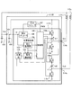
- FIG. 1 is a configuration diagram of the in-vehicle control device 113 according to the first embodiment.
- the in-vehicle control device 113 inductive load energization control device
- the inductance load 112 (inductive load) connected between the terminals 114 is energized and controlled. Thereby, the vehicle-mounted control apparatus 113 controls a vehicle.
- the battery terminal 101 is a terminal connected to the positive electrode of the external battery 100. Note that the negative electrode of the external battery 100 is connected via a ground.
- the inductance load 112 is a linear solenoid, for example, and controls the vehicle by energizing a desired current.
- the in-vehicle control device 113 flows a return current based on the counter electromotive force of the inductance load 112. The return current path uses a battery terminal 101 for the vehicle-mounted control device 113 to receive power supply from the external battery 100.
- the in-vehicle control device 113 includes an input capacitor 102, a microcomputer 107, and an ASIC (application specific integrated circuit) 117.
- the ASIC 117 includes a voltage regulator 106, a control unit 108, a limiting element 109, a drive element 110, a current detection element 111, a failure detection unit 105 including a voltage monitoring unit 103 and a current detection unit 104.
- the input side of the voltage regulator 106 is connected to the battery terminal 101.
- An input capacitor 102 is connected between the input side of the voltage regulator 106 and the ground in order to stabilize the input voltage Vi of the voltage regulator 106.
- the voltage regulator 106 generates a voltage necessary for the microcomputer 107 and the ASIC 117 to operate.
- the microcomputer 107 receives signals from various sensors installed outside the in-vehicle control device 113.
- the ASIC 117 of the in-vehicle control device 113 includes a limiting element 109 and a driving element 110 as switch elements for energizing the inductance load 112.
- a connection node between the limiting element 109 and the driving element 110 is connected to the inductance load 112 through the output terminal 114.
- the drive element 110 controls energization of the inductance load 112.
- the limiting element 109 causes a return current based on the counter electromotive force of the inductance load 112 to flow from the output terminal 114 to the battery terminal 101, and limits the current in the reverse direction.
- the drive element 110 and the limiting element 109 are configured using MOSFETs (metal-oxide-semiconductor field-effect transistors).
- the drain of the driving element 110 is connected to the output terminal 114, and the source of the driving element 110 is connected to the ground.
- the gate of the driving element 110 is connected to the control unit 108.
- the source of the limiting element 109 is connected to the drain of the driving element 110 and the output terminal 114 through the current detection element 111.
- a parasitic diode is formed from the source to the drain of the limiting element 109.
- the drain of the limiting element 109 is connected to the output terminal 114 and the input side of the voltage regulator 106.
- the gate of the limiting element 109 is connected to the control unit 108.
- the limiting element 109 can limit the current from the input side of the voltage regulator 106 to the driving element 110.
- the microcomputer 107 outputs a PWM (Pulse Width Modulation) signal to the control unit 108 in order to cause a desired current to flow through the inductance load 112.
- PWM Pulse Width Modulation
- the control unit 108 switches the limiting element 109 and the driving element 110 alternately between conduction (hereinafter referred to as “on”) and non-conduction (hereinafter referred to as “off”) based on the input PWM signal.
- the in-vehicle control device 113 can cause a desired current to flow through the inductance load 112.
- the driving element 110 when the driving element 110 is on and the limiting element 109 is off, a current flows from the external battery 100 in the order of the inductance load 112, the output terminal 114, the driving element 110, and the ground. As a result, energy is stored in the inductance load 112.
- the driving element 110 is turned off and the limiting element 109 is turned on, a return current is generated in the path of the inductance load 112, the output terminal 114, the limiting element 109, and the battery terminal 101 based on the back electromotive force generated in the inductance load 112. Flowing.
- the vehicle-mounted control device 113 energizes the inductance load 112 by such on / off control.
- the failure detection unit 105 detects an open failure of the battery terminal 101 and includes a voltage monitoring unit 103 and a current detection unit 104. When the open failure of the battery terminal 101 is detected, the failure detection unit 105 notifies the control unit 108 of the failure. When the open failure of the battery terminal 101 is notified, the control unit 108 performs control to shift the driving element 110 and the limiting element 109 to a predetermined state.
- the current detection element 111 is a shunt resistor, for example, and detects a current Io flowing through the limiting element 109.
- the current detection unit 104 detects whether or not the current Io detected by the current detection element 111 is within a predetermined range, and outputs it to the control unit 108. As a result, the failure detection unit 105 can notify the control unit 108 of the failure.
- the voltage monitoring unit 103 is for monitoring the input voltage Vi of the voltage regulator 106.
- the voltage monitoring unit 103 outputs information related to the input voltage Vi to the control unit 108, and if the input voltage Vi exceeds a predetermined overvoltage threshold or falls below a low voltage threshold, the control unit 108 and the current Notify the detection unit 104.
- the external battery 100 supplies power to the in-vehicle control device 113 through the battery terminal 101. Therefore, when a contact failure or the like of the battery terminal 101 occurs and an open failure occurs in the battery terminal 101, the power supply path from the external battery 100 to the in-vehicle control device 113 is cut off.
- the battery terminal 101 is also used as a path for flowing a return current based on the counter electromotive force generated in the inductance load 112 when the drive element 110 is turned off. When an open failure occurs in the battery terminal 101, the return current path is also disconnected.
- the input voltage Vi of the voltage regulator 106 is lower than the output voltage Vcc of the external battery 100.
- This voltage drop is caused by current consumption of the microcomputer 107 and the ASIC 117 (processing means).
- the voltage regulator 106 outputs a voltage corresponding to the input voltage Vi and applies it to the microcomputer 107 and the ASIC 117. If the output voltage of the voltage regulator 106 is higher than the voltage required to operate the microcomputer 107 and the ASIC 117, the microcomputer 107 and the ASIC 117 can continue to operate.
- the voltage monitoring unit 103 and the control unit 108 incorporated in the ASIC 117 can continue the voltage monitoring process.
- the microcomputer 107 notifies the vehicle occupant of the occurrence of an abnormality through a failure detection lamp or the like, notifies the other vehicle-mounted control device using the communication means of the occurrence of an abnormality, or processes for shifting the vehicle to a safe state. Can be controlled continuously.
- the drive element 110 When the drive element 110 is on, power cannot be supplied from the external battery 100 to the voltage regulator 106 via the inductance load 112, the output terminal 114, and the limiting element 109.
- the limiting element 109 and the driving element 110 are turned on and off periodically and alternately, energy is accumulated in the inductance load 112 during the on period of the driving element 110, and is generated in the inductance load 112 during the on period of the limiting element 109.
- the input capacitor 102 is charged based on the back electromotive force.
- the input capacitor 102 has a sufficient capacitance to supply power to the microcomputer 107 and the ASIC 117, and the microcomputer 107 can be continuously operated.
- the voltage regulator 106 cannot generate a voltage for operating the microcomputer 107, and the operation of the microcomputer 107 stops.
- a booster circuit that increases the input voltage Vi of the voltage regulator 106 can be configured.
- the limiting element 109 and the driving element 110 are turned on and off periodically and alternately to operate this booster circuit, thereby generating the input voltage Vi of the voltage regulator 106 and a voltage necessary for operating the microcomputer 107. It is possible to boost the voltage to a predetermined set voltage Vd.
- the driving element 110 and the limiting element 109 are turned on and off periodically and alternately. Energy is stored in the inductance load 112 during the ON period of the drive element 110, and the input capacitor 102 is charged through the limiting element 109 by a current based on the counter electromotive force generated in the inductance load 112 due to the turn-off of the drive element 110. As a result, the input voltage Vi of the voltage regulator 106 is boosted. Further, the voltage monitoring unit 103 detects the input voltage Vi of the voltage regulator 106. The control unit 108 performs on / off control by changing the on-duty of the drive element 110 so that the input voltage Vi detected by the voltage monitoring unit 103 becomes a predetermined set voltage Vd.
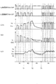
- the period P1 shown in FIG. 2 is before an open failure of the battery terminal 101 occurs.
- the period P2 is a period until the operation of the limiting element 109 and the driving element 110 is stopped after the open failure of the battery terminal 101 occurs.
- the period P3 is a period in which the on / off control of the limiting element 109 and the driving element 110 is stopped to determine the failure factor.
- the period P4 is a period in which the booster circuit including the external battery 100, the inductance load 112, the limiting element 109, the driving element 110, and the input capacitor 102 is operated to boost the input voltage Vi of the voltage regulator 106.
- FIG. 2A shows the on / off state of the limiting element 109.
- FIG. 2B shows the on / off state of the drive element 110.
- FIG. 2C shows the voltage Vo at the output terminal 114.
- FIG. 2D shows the current Io flowing through the limiting element 109.
- FIG. 2E shows the input voltage Vi of the voltage regulator 106.
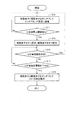
- FIG. 3 is a flowchart for explaining failure detection processing.
- a period P1 in FIG. 2 shows a state before an open failure of the battery terminal 101 occurs.
- typical signal states in the period P1 will be described.
- the limiting element 109 and the driving element 110 are turned on and off periodically and alternately to energize the inductance load 112 (step S10 in FIG. 3). ).
- the voltage Vo at the output terminal 114 becomes a voltage near the ground.
- the voltage Vo rises based on the counter electromotive force generated in the inductance load 112 and is clamped by the output voltage Vcc of the external battery 100. Therefore, the voltage Vo is near the output voltage Vcc.
- the limiting element 109 has a back electromotive force generated in the inductance load 112 due to the turning off of the driving element 110. Based on the current Io flows.
- This current Io is a reflux current.
- the limiting element 109 is off and the driving element 110 is on, no reflux current flows through the limiting element 109, and the current Io is approximately 0 amperes.
- the input side of the voltage regulator 106 is electrically connected to the external battery 100. Therefore, as shown in FIG. 2 (e), the input voltage Vi of the voltage regulator 106 becomes equal to the output voltage Vcc of the external battery 100.
- a time T1 in FIG. 2 indicates a time when the battery terminal 101 has an open failure.
- a period P2 in FIG. 2 indicates time T1 and after and until time T2 when the on / off operation of the limiting element 109 and the driving element 110 is stopped.
- typical signal states in the period P2 in FIG. 2 will be described.
- the limiting element 109 and the driving element 110 are alternately turned on and off to energize the inductance load 112 (step S10 in FIG. 3).
- the battery terminal 101 has an open failure at time T1
- the path through which the return current based on the counter electromotive force generated in the inductance load 112 is disconnected. Therefore, the reflux current does not flow.
- the current based on the counter electromotive force generated in the inductance load 112 due to the turn-off of the driving element 110 is charged to the input capacitor 102 via the limiting element 109 that is turned on. Therefore, as shown in FIG. 2E, the input voltage Vi of the voltage regulator 106 increases.
- the driving element 110 is turned on and the limiting element 109 is turned off, power is supplied from the energy charged in the input capacitor 102 to the microcomputer 107, so the input voltage Vi of the voltage regulator 106 decreases.
- the voltage Vo at the output terminal 114 becomes 0 V, which is a voltage near the ground, during the period P2 and when the limiting element 109 is off and the driving element 110 is on.
- the voltage Vo at the output terminal 114 is not clamped to the output voltage Vcc of the external battery 100 due to an open failure of the battery terminal 101.
- the input voltage Vi of the voltage regulator 106 increases based on the counter electromotive force generated in the inductance load 112 due to the turn-off of the driving element 110, the voltage Vo of the output terminal 114 also increases.
- the current Io flowing through the limiting element 109 based on the back electromotive force generated in the inductance load 112 is charged to the input capacitor 102 when the limiting element 109 is on and the driving element 110 is off.
- the input voltage Vi of the voltage regulator 106 gradually increases, and the current Io gradually decreases.
- the current Io of the limiting element 109 does not flow, and therefore becomes almost 0 amperes.
- the voltage regulator 106 is not supplied with power from the external battery 100 via the battery terminal 101. As shown in FIG. 2 (e), the input voltage Vi of the voltage regulator 106 increases. The voltage regulator 106 continues to generate a voltage necessary for the microcomputer 107 to operate. The microcomputer 107 continues to transmit a PWM signal to the control unit 108 in order to cause a predetermined current to flow through the inductance load 112. As a result, the back electromotive force is continuously generated in the inductance load 112. Therefore, the input voltage Vi of the voltage regulator 106 continues to rise and finally rises to the breakdown voltage of the voltage regulator 106. As a result, the voltage regulator 106 may be permanently damaged.
- the voltage monitoring unit 103 detects the input voltage Vi of the voltage regulator 106 (step S11 in FIG. 3), and a predetermined voltage (hereinafter referred to as an overvoltage threshold Vu) set lower than the breakdown voltage of the voltage regulator 106. When it exceeds, it determines with overvoltage, and notifies the control part 108 (time T2 of FIG. 2: Step S11-> Yes of FIG. 3). Receiving the overvoltage notification, the control unit 108 fixes the limiting element 109 on and the driving element 110 off to prevent the input voltage Vi of the voltage regulator 106 from increasing (step S12 in FIG. 3). That is, the control unit 108 stops the on / off control of the limiting element 109 and the driving element 110.
- Vu a predetermined voltage
- a time T2 in FIG. 2 is a time when the input voltage Vi of the voltage regulator 106 exceeds the overvoltage threshold Vu.
- a period P3 in FIG. 2 is a period from time T2 until the input voltage Vi of the voltage regulator 106 falls below the low voltage threshold Vb.
- a surge voltage may be superimposed on the input of the voltage regulator 106.
- the generation of the surge voltage is temporary, and after the generation of the surge voltage, the input voltage Vi of the voltage regulator 106 returns to the output voltage Vcc of the external battery 100 (the broken line in the period P3 in FIG. 2E). ). Therefore, it is desirable to return to the process of step S10 after the return and resume the energization control of the inductance load 112.
- the input voltage Vi of the voltage regulator 106 exceeds the overvoltage, and the voltage regulator 106 may reach a permanent failure. In such a case, it is desirable to turn on / off the limiting element 109 and the driving element 110 so that the input voltage Vi becomes a predetermined voltage.
- the current detection element 111 and the current detection unit 104 detect the current Io flowing through the limiting element 109. ing.
- the consumption current Iu of the microcomputer 107 and the ASIC 117 is changed from the external battery 100 to the inductance load 112, the output terminal 114, the limiting element 109, and the voltage regulator. It flows via 106.
- the current detection element 111 detects the consumption current Iu by the microcomputer 107 and the ASIC 117 (solid line in the period P3 in FIG. 2D).
- the consumption current Iu of the microcomputer 107 and the ASIC 117 flows from the external battery 100 via the battery terminal 101 and the voltage regulator 106.
- the current Io detected by the current detection element 111 is in the vicinity of 0 amperes (broken line in the period P3 in FIG. 2D).
- the current detection unit 104 detects the current Io flowing through the limiting element 109 by the current detection element 111 (step S13).
- the current Io is equal to or greater than a predetermined current threshold set lower than the minimum current consumption of the microcomputer 107 and the ASIC 117 (step S13 ⁇ No)
- the current detection unit 104 notifies the control unit 108 to that effect.
- the process proceeds to step S14.
- the current detection unit 104 notifies the control unit 108 to that effect.
- the control unit 108 determines that it is an overvoltage due to a surge voltage, and returns to the process of step S10.
- step S14 the voltage monitoring unit 103 determines whether or not the input voltage Vi of the voltage regulator 106 has fallen below the low voltage threshold Vb, and notifies the control unit 108 of the determination. If the input voltage Vi of the voltage regulator 106 is equal to or higher than the low voltage threshold Vb (step S14 ⁇ No), the control unit 108 returns to the process of step S13. As shown at time T3 in FIG. 2, if the input voltage Vi of the voltage regulator 106 falls below the low voltage threshold Vb (step S14 ⁇ Yes), the control unit 108 determines that there is an open failure of the battery terminal 101. The process proceeds to step S15.
- Time T3 in FIG. 2 is the time when the input of the voltage regulator 106 falls below the low voltage threshold Vb.
- a period P4 in FIG. 2 indicates a period after time T3.
- the control unit 108 performs the process of step S15. That is, the control unit 108 performs the boosting operation by controlling the limiting element 109 and the driving element 110 on / off at a frequency higher than that during the on / off control in step S10 (step S15).
- the frequency of the on / off control in step S15 is several to several tens of times higher than the frequency of the on / off control in step S10.
- FIG. 2 schematically shows the pulse period and the duty.
- a booster circuit can be formed by the inductance load 112, the limiting element 109, the driving element 110, and the input capacitor 102.
- the voltage monitoring unit 103 detects the input voltage Vi of the voltage regulator 106 and outputs it to the control unit 108.
- the control unit 108 performs feedback control by changing the on-duty of the drive element 110 so that the input voltage Vi of the voltage regulator 106 becomes a predetermined set voltage Vd.
- the set voltage Vd is higher than the minimum input voltage value for generating a voltage necessary for operating the microcomputer 107 and the ASIC 117. Therefore, the operation of the microcomputer 107 and the ASIC 117 is continued without being affected by the voltage drop due to the inductance load 112 and the limiting element 109, the consumption current of the microcomputer 107 and the ASIC 117, and the decrease of the output voltage Vcc due to the deterioration of the external battery 100. be able to.
- the principle of boosting the input voltage Vi of the voltage regulator 106 is the same as that shown in the period P2 in FIG.
- the control unit 108 does not depend on the PWM signal from the microcomputer 107, and turns on / off the limiting element 109 and the drive element 110 so that the input voltage Vi detected by the voltage monitoring unit 103 is maintained at a predetermined set voltage Vd. Turn off control.
- the control unit 108 performs on / off control of the limiting element 109 and the driving element 110 at a frequency higher than that of the period P1. Thereby, the fluctuation
- step S15 the input voltage Vi of the voltage regulator 106 is maintained at the predetermined set voltage Vd, and the microcomputer 107 and the ASIC 117 can continue to operate.
- the voltage monitoring unit 103 and the control unit 108 incorporated in the ASIC 117 can continue the voltage monitoring process.
- the microcomputer 107 notifies the vehicle occupant of the occurrence of an abnormality through a failure detection lamp or the like, notifies the other vehicle-mounted control device using the communication means of the occurrence of an abnormality, or processes for shifting the vehicle to a safe state. Can be controlled continuously.
- FIG. 4 is a configuration diagram of the in-vehicle control device 113A according to the second embodiment of the present invention.
- the difference from the first embodiment is that the limiting element 109, which is a MOSFET, is replaced with a limiting element 109A, which is a diode, and other equivalent parts are denoted by the same reference numerals and description thereof is omitted.
- the in-vehicle control device 113A may have a function equivalent to that of the MOSFET limiting element 109 described in the second embodiment even when a diode is used as the limiting element 109A. Is possible.
- a diode is used as the limiting element 109A, there is a problem that the voltage drop is large and the power consumption is large when the return current based on the counter electromotive force generated in the inductance load 112 flows as compared with the case where the MOSFET is used.
- the circuit of the in-vehicle control device 113A is simplified, and the energization control of the inductance load 112 can be simplified.
- FIG. 5 is a configuration diagram of the in-vehicle control device 113B according to the third embodiment of the present invention.
- the in-vehicle control device 113 of the first embodiment drives one inductance load 112, and the limiting element 109, the driving element 110, the current detection element 111, and the output terminal 114 combined with the inductance load 112 are one set.
- the vehicle-mounted control device 113B (inductive load energization control device) of the third embodiment is driven by the first inductance load 112b and the second inductance load 112c.
- the first limiting element 109b What is combined with the first inductance load 112b is the first limiting element 109b, the first drive element 110b, the first current detection element 111b, and the first output terminal 114b.
- the second inductance load 112c What is combined with the second inductance load 112c is the second limiting element 109c, the second drive element 110c, the second current detection element 111c, and the second output terminal 114c.
- On / off control of the combination of the first limiting element 109b and the first driving element 110b and the combination of the second limiting element 109c and the second driving element 110c are performed by the control unit 108, respectively.
- the in-vehicle control device 113B further includes an addition unit 115 that adds the current Io1 detected by the first current detection element 111b and the current Io2 detected by the second current detection element 111c.
- an addition unit 115 that adds the current Io1 detected by the first current detection element 111b and the current Io2 detected by the second current detection element 111c.
- Other parts equivalent to those of the vehicle-mounted control device 113 of the first embodiment are denoted by the same reference numerals and description thereof is omitted.
- the microcomputer 107 outputs a PWM signal corresponding to each of the first inductance load 112b and the second inductance load 112c to the control unit 108 in order to energize each of the first inductance load 112b and the second inductance load 112c.
- the control unit 108 performs on / off control of the first limiting element 109b and the first driving element 110b, and the second limiting element 109c and the second driving element 110c in accordance with each input PWM signal.
- the voltage monitoring unit 103 detects an overvoltage at the input of the voltage regulator 106, as shown in the first embodiment, it is determined whether or not the cause of the overvoltage is due to an open failure of the battery terminal 101.
- the first limiting element 109b is turned on, the first driving element 110b is turned off, the second limiting element 109c is turned on, and the second driving element 110c is turned off.
- the current Io1 flowing through the first limiting element 109b is detected by the first current detecting element 111b
- the current Io2 flowing through the second limiting element 109c is detected by the second current detecting element 111c.
- the consumption current of the microcomputer 107 and the ASIC 117 flows through the first limiting element 109b and the second limiting element 109c.
- the current value obtained by adding the currents Io1 and Io2 by the adding unit 115 is set lower than the minimum current consumption of the microcomputer 107 and the ASIC 117. Over a predetermined current threshold.
- the cause of the overvoltage is a surge voltage superimposed on the input of the voltage regulator 106, the calculated current consumption value is approximately 0 amperes, which is less than a predetermined current threshold.
- the voltage monitoring unit 103 detects a low voltage at the input of the voltage regulator 106 and determines that the cause of the overvoltage is an open failure of the battery terminal 101, the voltage is increased by the booster circuit as in the first embodiment.
- the input of the regulator 106 is boosted to a predetermined voltage value and maintained.
- the booster circuit can be constituted by one of the combination of the inductance load, the limiting element, and the driving element, and the input capacitor 102. Therefore, it is not necessary to form a booster circuit using the other combination and the input capacitor 102.
- a combination of the first inductance load 112b, the first limiting element 109b and the first driving element 110b and the input capacitor 102 constitute a booster circuit
- the second inductance load 112c, the second limiting element 109c A case where a booster circuit is not configured by the combination of the driving elements 110c is shown.
- the booster circuit boosts and maintains the input voltage Vi of the voltage regulator 106 to a voltage higher than the output voltage Vcc of the external battery 100.
- the second limiting element 109c causes an open failure of the battery terminal 101. It is turned on for current detection to determine whether or not it is due to. Therefore, it flows out from the input side of the voltage regulator 106 to the external battery 100 through the second limiting element 109c, the second output terminal 114c, and the second inductance load 112c.
- the second limiting element 109c is used while the boost operation is performed by the combination of the first inductance load 112b, the first limiting element 109b and the first driving element 110b and the input capacitor 102. Is turned off to prevent the current flowing from the input of the voltage regulator 106 to the external battery 100.
- the configuration used for the booster circuit is a combination of the first inductance load 112b, the first limiting element 109b, and the first driving element 110b, and a combination of the second inductance load 112c, the second limiting element 109c, and the second driving element 110c. Any one of them is used, and which combination is used is determined according to the use of the first inductance load 112b and the second inductance load 112c.
- the first inductance load 112b of the third embodiment relates to, for example, an energy saving operation of the vehicle, and does not have a great influence on the vehicle control even when a current due to the boosting operation flows.
- the second inductance load 112c relates to the operation of the transmission, for example, and if a current due to the boosting operation flows, the vehicle control is greatly affected. Therefore, in the third embodiment, the step-up operation may be performed by the combination of the first inductance load 112b, the first limiting element 109b, and the first driving element 110b and the input capacitor 102.
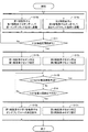
- FIG. 6 is a flowchart for explaining failure detection processing.
- the control unit 108 performs on / off control of the first limiting element 109b and the first driving element 110b to energize the first inductance load 112b (step S10b).
- the control unit 108 performs on / off control of the second limiting element 109c and the second drive element 110c to energize the second inductance load 112c (step S10c).
- the return current path based on the back electromotive force generated in the first inductance load 112b and the return current path based on the back electromotive force generated in the second inductance load 112c are disconnected. Therefore, the reflux current does not flow.
- the current based on the counter electromotive force generated in the first inductance load 112b due to the turn-off of the first driving element 110b is charged to the input capacitor 102 via the first limiting element 109b that is turned on.
- the current based on the counter electromotive force generated in the second inductance load 112c due to the turn-off of the second driving element 110c is charged to the input capacitor 102 via the second limiting element 109c that is turned on.
- the input voltage Vi of the voltage regulator 106 gradually increases, and the currents Io1 and Io2 gradually decrease.
- the voltage monitoring unit 103 detects the input voltage Vi of the voltage regulator 106 (step S11), and when the voltage exceeds a predetermined voltage set lower than the breakdown voltage of the voltage regulator 106 (hereinafter referred to as an overvoltage threshold Vu), the overvoltage is detected. And notifies the control unit 108 (step S11 ⁇ Yes in FIG. 3). Receiving the overvoltage notification, the control unit 108 fixes the first limiting element 109b on and the first driving element 110b off to prevent the input voltage Vi of the voltage regulator 106 from increasing (step S12b). Further, in parallel with the process of step S12b, the control unit 108 fixes the second limiting element 109c on and the second driving element 110c off (step S12c).
- the first current detection element 111b detects the current Io1 flowing through the first limiting element 109b.
- the second current detection element 111c detects a current Io2 flowing through the second limiting element 109c.
- the adder 115 calculates the sum of these currents Io1 and Io2.
- the current detection unit 104 notifies the control unit 108 of that fact. Notify The control unit 108 determines that it is an overvoltage due to a surge voltage, and returns to the parallel processing of steps S10b and S10c.
- step S13B ⁇ No If the sum of the currents Io1 and Io2 is equal to or greater than the predetermined current threshold (step S13B ⁇ No), the current detection unit 104 notifies the control unit 108 of that fact, and the control unit 108 proceeds to the process of step S14.
- step S14 the voltage monitoring unit 103 determines whether or not the input voltage Vi of the voltage regulator 106 has fallen below the low voltage threshold value Vb, and notifies the control unit 108 to that effect. If the input voltage Vi of the voltage regulator 106 is equal to or higher than the low voltage threshold Vb (step S14 ⁇ No), the control unit 108 returns to the process of step S13B. If the input voltage Vi of the voltage regulator 106 falls below the low voltage threshold Vb (step S14 ⁇ Yes), the control unit 108 determines that there is an open failure of the battery terminal 101, and proceeds to parallel processing of steps S15b and S15c. .
- the control unit 108 performs a step-up operation by controlling on / off of the first limiting element 109b and the first driving element 110b at a frequency higher than that in step S10 (step S15b).
- a boost circuit can be formed by the first inductance load 112b, the first limiting element 109b, and the input capacitor 102.
- the control unit 108 fixes the second limiting element 109c and the second drive element 110c off (step S15c).
- the voltage monitoring unit 103 detects the input voltage Vi of the voltage regulator 106 and outputs it to the control unit 108.
- the control unit 108 performs feedback control with a predetermined duty so that the input voltage Vi of the voltage regulator 106 becomes a predetermined set voltage Vd.
- the set voltage Vd is higher than the minimum input voltage value for the voltage regulator 106 to generate a voltage necessary for operating the microcomputer 107 and the ASIC 117. Therefore, the voltage drop due to the first inductance load 112b and the first limiting element 109b, the voltage drop due to the second inductance load 112c and the second limiting element 109c, the consumption current of the microcomputer 107 and the ASIC 117, and the output due to the deterioration of the external battery 100 The operation of the microcomputer 107 and the ASIC 117 can be continued without being affected by the decrease in the voltage Vcc. As a result, the voltage monitoring unit 103 and the control unit 108 incorporated in the ASIC 117 can continuously perform the voltage monitoring process.
- the microcomputer 107 notifies the vehicle occupant of the occurrence of an abnormality through a failure detection lamp or the like, notifies the other vehicle-mounted control device using the communication means of the occurrence of an abnormality, or processes for shifting the vehicle to a safe state. Can be controlled continuously.
- the set voltage Vd needs to be set to be equal to or higher than the voltage obtained by subtracting the forward voltage drop of the parasitic diode of the MOSFET from the output voltage Vcc of the external battery 100. This is because if the set voltage Vd is lower than this voltage, the external battery 100 is discharged to the battery terminal 101 and attenuated through the inductance load that is not energized and the parasitic diode of the limiting element.
- the booster circuit may be configured by a combination of an inductance load that does not greatly affect the control of the vehicle and the limiting element and the driving element, and the limiting element and the driving element related to other combinations may be turned off.
- the present invention is not limited to the embodiments described above, and includes various modifications.
- the above-described embodiment has been described in detail for easy understanding of the present invention, and is not necessarily limited to the one having all the configurations described.
- a part of the configuration of one embodiment can be replaced with the configuration of another embodiment, and the configuration of another embodiment can be added to the configuration of one embodiment.
- a part or all of the above-described configurations, functions, processing units, processing means, and the like may be realized by hardware such as an integrated circuit.
- Each of the above-described configurations, functions, and the like may be realized by software by a processor interpreting and executing a program that realizes each function.
- Information such as programs, tables, and files for realizing each function may be stored in a recording device such as a memory, a hard disk, or an SSD (Solid State Drive), or a recording medium such as a flash memory card or a DVD (Digital Versatile Disk). it can.
- control lines and information lines indicate what is considered necessary for the explanation, and not all control lines and information lines on the product are necessarily shown. Actually, it may be considered that almost all the components are connected to each other. Examples of modifications of the present invention include the following (a) to (g).
- the failure detection unit 105 including the voltage monitoring unit 103 and the current detection unit 104 is configured in the ASIC 117, but is not limited thereto, and may be embodied by software executed by the microcomputer 107.
- the microcomputer 107 and software functions executed thereby may be embodied by the ASIC 117.
- the drive element 110 is not limited to a MOSFET, and may be a switch element.
- the limiting element 109 is not limited to a MOSFET, but may be a parallel circuit of a switch element and a diode, or a diode.
- the inductive load energization control device of the present invention is not limited to a vehicle-mounted control device, and may be mounted on a moving body such as a ship, an aircraft, or the like, and further mounted on a building or a home appliance device or the like. Load energization control may be performed.
- each limiting element may be configured by a diode.
- the determination in step S14 in FIG. 2 is not limited to the voltage determination on the input side of the voltage regulator 106, and a determination condition may be that a predetermined time has elapsed after step S12.
Landscapes
- Physics & Mathematics (AREA)
- General Physics & Mathematics (AREA)
- Testing Of Short-Circuits, Discontinuities, Leakage, Or Incorrect Line Connections (AREA)
- Charge And Discharge Circuits For Batteries Or The Like (AREA)
- Electronic Switches (AREA)
Abstract
外部バッテリの電源供給経路と、誘導性負荷の還流電流経路が同一端子を使用している装置において、この端子がオープン故障した後でもマイクロコンピュータの動作を継続させる。 車載制御装置113は、外部バッテリ100と接続するバッテリ端子101と、バッテリ端子101に入力側が接続された電圧レギュレータ106と、電圧レギュレータ106の入力側とグランドとの間に設けられる入力コンデンサ102と、インダクタンス負荷112を通電制御する駆動素子110と、電圧レギュレータ106の入力側と駆動素子110との間に設けられた制限素子109と、駆動素子110をオン・オフ制御するマイクロコンピュータ107と、バッテリ端子101のオープン故障を判定する故障検知部105とを備える。故障検知部105は、バッテリ端子101のオープン故障を判定すると、駆動素子110を駆動させて入力電圧Viを維持する。
Description
本発明は、外部バッテリからコネクタの端子経由で電源供給を受けて、誘導性負荷に通電を行う機能を備えた誘導性負荷通電制御装置に関する。誘導性負荷通電制御装置は、例えば車両や船舶や航空機などの移動体に組み込まれて使用される。
車載制御装置は、誘導性負荷通電制御装置の一種であり、外部に設置された抵抗負荷やインダクタンス負荷(誘導性負荷)の通電制御を行うことで車両を制御する。車載制御装置は、外部バッテリからコネクタ端子を通じて電源供給を受け、電圧レギュレータによりマイクロコンピュータやその他IC(Integrated Circuit)などが動作するのに必要な電圧を生成する。車載制御装置のマイクロコンピュータは、この車載制御装置の外部に設置された各種センサからの信号を受信する。
車載制御装置によって通電制御されるインダクタンス負荷は、例えばリニアソレノイドであり、所望の電流の通電により車両を制御している。この時、インダクタンス負荷に発生する逆起電力に基づく還流電流を流している場合があるが、その還流電流の経路は、車載制御装置が外部バッテリから電源供給を受けるためのコネクタ端子を利用する場合がある。そのため、コネクタ端子に接触不良などが起き、オープン故障が発生した場合には、外部バッテリの電源供給経路と、インダクタンス負荷に所望の電流を流すための還流電流経路とが、切断されてしまう。
本発明の背景技術として、特許文献1がある。特許文献1の要約書の解決手段には、「グランド端子104が断線すると、電源端子103bとグランド端子104との間に接続された電源コンデンサ113が断続駆動されている誘導性負荷の転流電流によって充電されて電圧上昇し、これが所定の閾値を超過したことによってグランド配線の断線異常を検出して、給電開閉素子140a,140bを一斉遮断する。」と記載されている。
しかし、特許文献1に記載の発明では、全ての給電開閉素子に対して通電率100%の完全導通指令が与えられるようなことがあれば、誘導性負荷の正側電位が上昇して、電源コンデンサおよび定電圧電源に対する給電が停止する無給電状態となる。この無給電状態が持続すると電源コンデンサの充電電圧が放電減衰し、やがてマイクロプロセッサなどの処理手段が不作動状態になる。
本発明は前記課題を解決するために鑑みてなされたものであり、外部バッテリから電源供給を行う経路であると共に、誘導性負荷の還流電流の経路でもあるコネクタ端子がオープン故障した際であっても処理手段による動作を継続させて、誘導性負荷通電制御装置が完全な機能失陥になるのを防ぐことを課題とする。
前記した課題を解決するため、本発明の誘導性負荷通電制御装置は、外部バッテリと接続するバッテリ端子と、前記バッテリ端子に入力側が接続された電圧レギュレータと、前記電圧レギュレータの入力側とグランドとの間に設けられる入力コンデンサと、誘導性負荷の通電を制御する駆動素子と、前記電圧レギュレータの入力側と前記駆動素子との間に設けられて、前記電圧レギュレータの入力側から前記駆動素子への電流を制限可能な制限素子と、前記駆動素子をオン・オフ制御すると共に前記バッテリ端子がオープン故障しているか否かを判定する処理手段とを備える。前記処理手段は、前記バッテリ端子がオープン故障していると判定すると、前記駆動素子をオン・オフ制御して、前記誘導性負荷と前記駆動素子と前記制限素子と前記入力コンデンサとで構成される昇圧回路により前記電圧レギュレータの入力電圧を所定の電圧値に維持する。
その他の手段については、発明を実施するための形態のなかで説明する。
その他の手段については、発明を実施するための形態のなかで説明する。
本発明によれば、外部バッテリから電源供給を行う経路であると共に、誘導性負荷の還流電流の経路でもあるコネクタ端子がオープン故障した際であっても処理手段による動作を継続させて、誘導性負荷通電制御装置が完全な機能失陥になるのを防ぐことができる。
以降、本発明を実施するための形態を、各図を参照して詳細に説明する。
《第1の実施形態》
図1は、第1の実施形態における車載制御装置113の構成図である。
第1の実施形態の車載制御装置113(誘導性負荷通電制御装置)は、外部に設置された外部バッテリ100の正極からコネクタのバッテリ端子101を通じて電源供給を受け、この外部バッテリ100の正極と出力端子114との間に接続されるインダクタンス負荷112(誘導性負荷)を通電制御する。これにより車載制御装置113は、車両の制御を行う。
《第1の実施形態》
図1は、第1の実施形態における車載制御装置113の構成図である。
第1の実施形態の車載制御装置113(誘導性負荷通電制御装置)は、外部に設置された外部バッテリ100の正極からコネクタのバッテリ端子101を通じて電源供給を受け、この外部バッテリ100の正極と出力端子114との間に接続されるインダクタンス負荷112(誘導性負荷)を通電制御する。これにより車載制御装置113は、車両の制御を行う。
バッテリ端子101は、外部バッテリ100の正極に接続される端子である。なお、外部バッテリ100の負極は、グランドを介して接続される。
インダクタンス負荷112は、例えばリニアソレノイドであり、所望の電流の通電により車両を制御している。車載制御装置113は、インダクタンス負荷112の逆起電力に基づく還流電流を流す。その還流電流の経路は、車載制御装置113が外部バッテリ100から電源供給を受けるためのバッテリ端子101を利用している。
この車載制御装置113は、入力コンデンサ102、マイクロコンピュータ107、ASIC(application specific integrated circuit)117を備えている。ASIC117は、電圧レギュレータ106、制御部108、制限素子109、駆動素子110、電流検出素子111、電圧監視部103と電流検知部104を含む故障検知部105を含んで構成される。
電圧レギュレータ106の入力側は、バッテリ端子101に接続される。電圧レギュレータ106の入力側とグランドとの間には、電圧レギュレータ106の入力電圧Viを安定化させるために入力コンデンサ102が接続される。
電圧レギュレータ106は、マイクロコンピュータ107と、ASIC117が動作するのに必要な電圧を生成している。マイクロコンピュータ107は、この車載制御装置113の外部に設置された各種センサからの信号を受信する。
電圧レギュレータ106は、マイクロコンピュータ107と、ASIC117が動作するのに必要な電圧を生成している。マイクロコンピュータ107は、この車載制御装置113の外部に設置された各種センサからの信号を受信する。
また、車載制御装置113のASIC117は、インダクタンス負荷112に通電を行うためのスイッチ素子として制限素子109と駆動素子110を備える。制限素子109と駆動素子110の接続ノードは、出力端子114を通じてインダクタンス負荷112に接続している。
駆動素子110は、インダクタンス負荷112の通電を制御する。制限素子109は、インダクタンス負荷112の逆起電力に基づく還流電流を出力端子114からバッテリ端子101へ流し、その逆方向の電流を制限する。これら駆動素子110と制限素子109は、MOSFET(metal-oxide-semiconductor field-effect transistor)を用いて構成される。
駆動素子110は、インダクタンス負荷112の通電を制御する。制限素子109は、インダクタンス負荷112の逆起電力に基づく還流電流を出力端子114からバッテリ端子101へ流し、その逆方向の電流を制限する。これら駆動素子110と制限素子109は、MOSFET(metal-oxide-semiconductor field-effect transistor)を用いて構成される。
駆動素子110のドレインは出力端子114に接続され、駆動素子110のソースはグランドに接続される。駆動素子110のゲートは、制御部108に接続される。
制限素子109のソースは、電流検出素子111を通じて駆動素子110のドレインと出力端子114に接続される。制限素子109のソースからドレインに向けて寄生ダイオードが形成される。これにより、駆動素子110のオンと制限素子109のオンとの間に設けられたデットタイム(不図示)において、インダクタンス負荷112の逆起電力に基づく環流電流を制限素子109の寄生ダイオードを通じて流すことができる。制限素子109のドレインは、出力端子114および電圧レギュレータ106の入力側に接続される。制限素子109のゲートは、制御部108に接続される。制限素子109は、電圧レギュレータ106の入力側から駆動素子110への電流を制限可能である。
制限素子109のソースは、電流検出素子111を通じて駆動素子110のドレインと出力端子114に接続される。制限素子109のソースからドレインに向けて寄生ダイオードが形成される。これにより、駆動素子110のオンと制限素子109のオンとの間に設けられたデットタイム(不図示)において、インダクタンス負荷112の逆起電力に基づく環流電流を制限素子109の寄生ダイオードを通じて流すことができる。制限素子109のドレインは、出力端子114および電圧レギュレータ106の入力側に接続される。制限素子109のゲートは、制御部108に接続される。制限素子109は、電圧レギュレータ106の入力側から駆動素子110への電流を制限可能である。
マイクロコンピュータ107は、インダクタンス負荷112に所望の電流を流すためにPWM(Pulse Width Modulation)信号を制御部108に対して出力する。制御部108は、入力されたPWM信号を基に制限素子109と駆動素子110を交互に導通(以下、オンとする)と非導通(以下、オフとする)に切り替える。これにより、車載制御装置113は、インダクタンス負荷112に所望の電流を流すことができる。
具体的には、駆動素子110がオンし、制限素子109がオフしている時、外部バッテリ100からインダクタンス負荷112、出力端子114、駆動素子110、グランドの順番に電流が流れる。これによりインダクタンス負荷112にエネルギが蓄積される。
駆動素子110がオフし、制限素子109がオンしている時、インダクタンス負荷112に発生する逆起電力に基づき、インダクタンス負荷112、出力端子114、制限素子109、バッテリ端子101の経路に還流電流が流れる。このようなオン・オフ制御により車載制御装置113は、インダクタンス負荷112に通電を行う。
駆動素子110がオフし、制限素子109がオンしている時、インダクタンス負荷112に発生する逆起電力に基づき、インダクタンス負荷112、出力端子114、制限素子109、バッテリ端子101の経路に還流電流が流れる。このようなオン・オフ制御により車載制御装置113は、インダクタンス負荷112に通電を行う。
故障検知部105は、バッテリ端子101のオープン故障を検知するものであり、電圧監視部103と電流検知部104とを備える。バッテリ端子101のオープン故障を検出した場合、故障検知部105は、制御部108に故障を通知する。制御部108は、バッテリ端子101のオープン故障が通知されると、駆動素子110と制限素子109を所定の状態に移行させる制御を行う。
電流検出素子111は、例えばシャント抵抗であり、制限素子109に流れる電流Ioを検出している。電流検知部104は、電流検出素子111によって検出された電流Ioが所定の範囲内にあるか否かを検知して、制御部108に出力する。これにより故障検知部105は、制御部108に故障を通知することができる。
電圧監視部103は、電圧レギュレータ106の入力電圧Viを監視するためのものである。電圧監視部103は、入力電圧Viに係る情報を制御部108に出力すると共に、入力電圧Viが所定の過電圧閾値を超え、または低電圧閾値を下回ったならば、その旨を制御部108と電流検知部104に通知する。
電圧監視部103は、電圧レギュレータ106の入力電圧Viを監視するためのものである。電圧監視部103は、入力電圧Viに係る情報を制御部108に出力すると共に、入力電圧Viが所定の過電圧閾値を超え、または低電圧閾値を下回ったならば、その旨を制御部108と電流検知部104に通知する。
外部バッテリ100は、バッテリ端子101を通じて車載制御装置113へ電源を供給している。そのため、バッテリ端子101の接触不良などが起き、バッテリ端子101にオープン故障が発生した場合には、外部バッテリ100から車載制御装置113への電源供給の経路が切断されてしまう。また、バッテリ端子101は、駆動素子110のターンオフによりインダクタンス負荷112に発生する逆起電力に基づく還流電流を流す経路としても使われている。バッテリ端子101にオープン故障が発生すると、還流電流の経路も切断されてしまう。
しかしながら、バッテリ端子101のオープン故障により外部バッテリ100から車載制御装置113への電源供給経路が切断されても、駆動素子110がオフの時には、外部バッテリ100からインダクタンス負荷112、出力端子114、制限素子109を経由して、電圧レギュレータ106の入力に外部バッテリ100が接続される経路が存在する。そのため、バッテリ端子101のオープン故障が発生した後は、外部バッテリ100からインダクタンス負荷112、出力端子114、制限素子109を経由して、電圧レギュレータ106の入力側に電流が流れることになる。この電流は、マイクロコンピュータ107とASIC117の消費電流である。
この時、インダクタンス負荷112と制限素子109に流れる電流Ioによる電圧降下が発生し、電圧レギュレータ106の入力電圧Viは、外部バッテリ100の出力電圧Vccよりも低い電圧となる。この電圧降下は、マイクロコンピュータ107とASIC117(処理手段)の消費電流によって発生する。
電圧レギュレータ106は、入力電圧Viに応じた電圧を出力して、マイクロコンピュータ107とASIC117に印加する。電圧レギュレータ106の出力電圧が、マイクロコンピュータ107とASIC117を動作させるのに必要な電圧よりも高ければ、マイクロコンピュータ107とASIC117は動作の継続が可能となる。入力電圧Viが、この条件を満たす最低入力電圧値より高ければ、ASIC117に組み込まれた電圧監視部103と制御部108は、電圧監視処理を継続して行える。マイクロコンピュータ107は、故障検知ランプなどを通じた車両の乗員への異常発生の報知、通信手段を用いた他の車載制御装置への異常発生の通知、車両を安全な状態へ移行させるための処理などの制御を継続して行える。
電圧レギュレータ106は、入力電圧Viに応じた電圧を出力して、マイクロコンピュータ107とASIC117に印加する。電圧レギュレータ106の出力電圧が、マイクロコンピュータ107とASIC117を動作させるのに必要な電圧よりも高ければ、マイクロコンピュータ107とASIC117は動作の継続が可能となる。入力電圧Viが、この条件を満たす最低入力電圧値より高ければ、ASIC117に組み込まれた電圧監視部103と制御部108は、電圧監視処理を継続して行える。マイクロコンピュータ107は、故障検知ランプなどを通じた車両の乗員への異常発生の報知、通信手段を用いた他の車載制御装置への異常発生の通知、車両を安全な状態へ移行させるための処理などの制御を継続して行える。
なお、駆動素子110がオンの時には、外部バッテリ100からインダクタンス負荷112、出力端子114、制限素子109を経由した電圧レギュレータ106への電源供給もできなくなる。
制限素子109と駆動素子110が周期的かつ交互にオンとオフを繰り返すと、駆動素子110のオン期間中にインダクタンス負荷112にエネルギが蓄積され、制限素子109のオン期間中、インダクタンス負荷112に発生する逆起電力に基づき、入力コンデンサ102が充電される。入力コンデンサ102は、マイクロコンピュータ107とASIC117に電力を供給するのに十分な静電容量を持っており、このマイクロコンピュータ107に動作を継続させることが可能である。
制限素子109と駆動素子110が周期的かつ交互にオンとオフを繰り返すと、駆動素子110のオン期間中にインダクタンス負荷112にエネルギが蓄積され、制限素子109のオン期間中、インダクタンス負荷112に発生する逆起電力に基づき、入力コンデンサ102が充電される。入力コンデンサ102は、マイクロコンピュータ107とASIC117に電力を供給するのに十分な静電容量を持っており、このマイクロコンピュータ107に動作を継続させることが可能である。
一方、インダクタンス負荷112と制限素子109による電圧降下が大きい場合には、電圧レギュレータ106は、マイクロコンピュータ107を動作させるための電圧を生成することができず、マイクロコンピュータ107の動作が停止する。
しかし、外部バッテリ100とインダクタンス負荷112と制限素子109と駆動素子110と入力コンデンサ102を用いると、電圧レギュレータ106の入力電圧Viを上昇させる昇圧回路を構成可能である。制限素子109と駆動素子110が周期的かつ交互にオンとオフさせて、この昇圧回路を動作させることにより、電圧レギュレータ106の入力電圧Viを、マイクロコンピュータ107を動作させるのに必要な電圧を生成可能な、所定の設定電圧Vdにまで昇圧させることが可能である。
具体的には、駆動素子110と制限素子109を周期的かつ交互にオン・オフさせる。駆動素子110のオン期間にインダクタンス負荷112にエネルギを蓄積し、この駆動素子110のターンオフによりインダクタンス負荷112に発生する逆起電力に基づく電流により、制限素子109を通じて入力コンデンサ102に充電させる。これにより電圧レギュレータ106の入力電圧Viを昇圧させる。更に電圧監視部103は、電圧レギュレータ106の入力電圧Viを検出する。制御部108は、電圧監視部103が検出する入力電圧Viが所定の設定電圧Vdになるように、駆動素子110のオン・デューティを変化させてオン・オフ制御を行う。
以下、図2(a)~(e)を参照して車載制御装置113の動作を説明する。更に図3を参照して、故障検出処理を説明する。
図2に示した期間P1は、バッテリ端子101のオープン故障が発生する前である。期間P2は、バッテリ端子101のオープン故障が発生した後、制限素子109と駆動素子110の動作を停止するまでの期間である。期間P3は、制限素子109と駆動素子110のオン・オフ制御を停止して故障要因を判定する期間である。期間P4は、外部バッテリ100とインダクタンス負荷112と制限素子109と駆動素子110と入力コンデンサ102から成る昇圧回路を動作させて、電圧レギュレータ106の入力電圧Viを昇圧させる期間である。
図2に示した期間P1は、バッテリ端子101のオープン故障が発生する前である。期間P2は、バッテリ端子101のオープン故障が発生した後、制限素子109と駆動素子110の動作を停止するまでの期間である。期間P3は、制限素子109と駆動素子110のオン・オフ制御を停止して故障要因を判定する期間である。期間P4は、外部バッテリ100とインダクタンス負荷112と制限素子109と駆動素子110と入力コンデンサ102から成る昇圧回路を動作させて、電圧レギュレータ106の入力電圧Viを昇圧させる期間である。
図2(a)は、制限素子109のオン・オフ状態を示している。
図2(b)は、駆動素子110のオン・オフ状態を示している。
図2(c)は、出力端子114の電圧Voを示している。
図2(d)は、制限素子109に流れる電流Ioを示している。
図2(e)は、電圧レギュレータ106の入力電圧Viを示している。
図3は、故障検出処理を説明するフローチャートである。
図2(b)は、駆動素子110のオン・オフ状態を示している。
図2(c)は、出力端子114の電圧Voを示している。
図2(d)は、制限素子109に流れる電流Ioを示している。
図2(e)は、電圧レギュレータ106の入力電圧Viを示している。
図3は、故障検出処理を説明するフローチャートである。
《期間P1の説明》
図2の期間P1は、バッテリ端子101のオープン故障が発生する前の状態を示している。以下、期間P1における代表的な信号の状態を説明する。
期間P1において、図2(a),(b)に示すように、制限素子109と駆動素子110は、周期的かつ交互にオンとオフを繰り返してインダクタンス負荷112に通電させる(図3のステップS10)。
図2の期間P1は、バッテリ端子101のオープン故障が発生する前の状態を示している。以下、期間P1における代表的な信号の状態を説明する。
期間P1において、図2(a),(b)に示すように、制限素子109と駆動素子110は、周期的かつ交互にオンとオフを繰り返してインダクタンス負荷112に通電させる(図3のステップS10)。
期間P1において、図2(c)に示すように、制限素子109がオフで駆動素子110がオンの時、出力端子114の電圧Voは、グランド近傍の電圧となる。制限素子109がオンで駆動素子110がオフの時に、電圧Voは、インダクタンス負荷112に発生する逆起電力に基づいて上昇すると共に、外部バッテリ100の出力電圧Vccによりクランプされる。そのため電圧Voは、出力電圧Vcc近傍となる。
期間P1において、図2(d)に示すように、制限素子109がオンで駆動素子110がオフの時、制限素子109には、駆動素子110のターンオフによりインダクタンス負荷112に発生する逆起電力に基づく電流Ioが流れる。この電流Ioは還流電流である。制限素子109がオフで駆動素子110がオンの時、制限素子109には還流電流は流れず、電流Ioは、ほぼ0アンペアとなる。
期間P1において、電圧レギュレータ106の入力側は、外部バッテリ100に電気的に接続されている。そのため、図2(e)に示すように、電圧レギュレータ106の入力電圧Viは、外部バッテリ100の出力電圧Vccに等しくなる。
《期間P2の説明》
図2の時刻T1は、バッテリ端子101がオープン故障した時刻を示している。図2の期間P2は、時刻T1以降、かつ制限素子109と駆動素子110のオン・オフ動作が停止する時刻T2までを示している。以下、図2の期間P2における代表的な信号の状態を説明する。
図2の時刻T1は、バッテリ端子101がオープン故障した時刻を示している。図2の期間P2は、時刻T1以降、かつ制限素子109と駆動素子110のオン・オフ動作が停止する時刻T2までを示している。以下、図2の期間P2における代表的な信号の状態を説明する。
期間P2において、図2(a),(b)に示すように、制限素子109と駆動素子110は、交互にオンとオフを繰り返してインダクタンス負荷112に通電させる(図3のステップS10)。
時刻T1においてバッテリ端子101がオープン故障すると、インダクタンス負荷112に発生する逆起電力に基づく還流電流を流す経路は切断される。よって、還流電流は流れなくなる。その結果、駆動素子110のターンオフによりインダクタンス負荷112に発生する逆起電力に基づく電流は、オンしている制限素子109を経由して入力コンデンサ102に充電される。そのため、図2(e)に示す通り、電圧レギュレータ106の入力電圧Viは上昇する。一方、駆動素子110がオンし、制限素子109がオフ時には、入力コンデンサ102に充電されたエネルギからマイクロコンピュータ107に電力を供給するため、電圧レギュレータ106の入力電圧Viは低下する。
時刻T1においてバッテリ端子101がオープン故障すると、インダクタンス負荷112に発生する逆起電力に基づく還流電流を流す経路は切断される。よって、還流電流は流れなくなる。その結果、駆動素子110のターンオフによりインダクタンス負荷112に発生する逆起電力に基づく電流は、オンしている制限素子109を経由して入力コンデンサ102に充電される。そのため、図2(e)に示す通り、電圧レギュレータ106の入力電圧Viは上昇する。一方、駆動素子110がオンし、制限素子109がオフ時には、入力コンデンサ102に充電されたエネルギからマイクロコンピュータ107に電力を供給するため、電圧レギュレータ106の入力電圧Viは低下する。
図2(c)に示すように、出力端子114の電圧Voは、期間P2かつ制限素子109がオフで駆動素子110のオン時、グランド近傍の電圧である0Vとなる。制限素子109がオンで駆動素子110がオフ時に、出力端子114の電圧Voは、バッテリ端子101のオープン故障のため外部バッテリ100の出力電圧Vccにクランプされなくなる。更に駆動素子110のターンオフによりインダクタンス負荷112に発生する逆起電力に基づき、電圧レギュレータ106の入力電圧Viが上昇してゆくため、出力端子114の電圧Voも上昇してゆく。
図2(d)に示す通り、インダクタンス負荷112に発生する逆起電力に基づき制限素子109に流れる電流Ioは、制限素子109がオンで駆動素子110がオフの時には入力コンデンサ102へ充電される。この電流Ioにより電圧レギュレータ106の入力電圧Viが次第に上昇し、電流Ioは次第に減少してゆく。制限素子109がオフで駆動素子110がオンの時に、制限素子109の電流Ioは流れないため、ほぼ0アンペアとなる。
バッテリ端子101がオープン故障した後、電圧レギュレータ106には、外部バッテリ100からバッテリ端子101を経由した電源供給が行われなくなる。図2(e)に示した通り、電圧レギュレータ106の入力電圧Viは上昇してゆく。電圧レギュレータ106は、マイクロコンピュータ107が動作するのに必要な電圧を生成し続ける。マイクロコンピュータ107はインダクタンス負荷112に所定の電流を流すためにPWM信号を制御部108に送信し続ける。その結果、インダクタンス負荷112には連続的に逆起電力が発生し続けることになる。よって、電圧レギュレータ106の入力電圧Viは更に上昇を続け、最終的には電圧レギュレータ106の破壊電圧まで上昇する。これにより、電圧レギュレータ106が永久故障するおそれがある。
そのため、電圧監視部103は、電圧レギュレータ106の入力電圧Viを検出し(図3のステップS11)、電圧レギュレータ106の破壊電圧よりも低く設定した所定の電圧(以下、過電圧閾値Vuとする)を超えた場合に過電圧と判定して、制御部108に通知する(図2の時刻T2:図3のステップS11→Yes)。過電圧の通知を受けた制御部108は、電圧レギュレータ106の入力電圧Viの上昇を防止するため、制限素子109をオンに、駆動素子110をオフに固定させる(図3のステップS12)。つまり、制御部108は、制限素子109と駆動素子110のオン・オフ制御を停止する。
《期間P3の説明》
図2の時刻T2は、電圧レギュレータ106の入力電圧Viが過電圧閾値Vuを超える時刻である。図2の期間P3は、時刻T2以降、かつ電圧レギュレータ106の入力電圧Viが低電圧閾値Vbを下回るまでの期間である。
時刻T2において電圧監視部103が、電圧レギュレータ106の入力の過電圧を検出する要因として、バッテリ端子101のオープン故障の他に、電圧レギュレータ106の入力にサージ電圧が重畳される場合がある。
図2の時刻T2は、電圧レギュレータ106の入力電圧Viが過電圧閾値Vuを超える時刻である。図2の期間P3は、時刻T2以降、かつ電圧レギュレータ106の入力電圧Viが低電圧閾値Vbを下回るまでの期間である。
時刻T2において電圧監視部103が、電圧レギュレータ106の入力の過電圧を検出する要因として、バッテリ端子101のオープン故障の他に、電圧レギュレータ106の入力にサージ電圧が重畳される場合がある。
一般的にサージ電圧の発生は一時的であり、サージ電圧の発生後は、電圧レギュレータ106の入力電圧Viは、外部バッテリ100の出力電圧Vccに復帰する(図2(e)の期間P3における破線)。よって、復帰後はステップS10の処理に戻り、インダクタンス負荷112の通電制御を再開させることが望ましい。
一方、バッテリ端子101がオープン故障すると、電圧レギュレータ106の入力電圧Viが過電圧を超えて、電圧レギュレータ106が永久故障に至るおそれがある。このような場合には、入力電圧Viが所定電圧になるように制限素子109と駆動素子110をオン・オフ制御することが望ましい。
つまり、電圧レギュレータ106の入力に過電圧が発生した要因ごとに、制限素子109と駆動素子110の制御を分けることが望ましく、そのためには、過電圧が発生した要因がバッテリ端子101のオープン故障に因るものか否かを判定する必要がある。
過電圧が発生した要因がバッテリ端子101のオープン故障に因るものか否かを判定するために、本実施形態では、電流検出素子111と電流検知部104により制限素子109に流れる電流Ioを検知している。
この時、過電圧が発生した要因がバッテリ端子101のオープン故障である場合には、マイクロコンピュータ107とASIC117の消費電流Iuが、外部バッテリ100からインダクタンス負荷112、出力端子114、制限素子109、電圧レギュレータ106を経由して流れる。電流検出素子111は、マイクロコンピュータ107とASIC117による消費電流Iuを検出することになる(図2(d)の期間P3における実線)。
一方、過電圧が発生した要因がサージ電圧に因るものである場合には、マイクロコンピュータ107とASIC117の消費電流Iuは、外部バッテリ100からバッテリ端子101、電圧レギュレータ106を経由して流れる。電流検出素子111が検出する電流Ioは、0アンペア近傍になる(図2(d)の期間P3における破線)。
よって、期間P3において、電流検知部104は、電流検出素子111によって制限素子109に流れる電流Ioを検出する(ステップS13)。この電流Ioがマイクロコンピュータ107とASIC117の最小消費電流よりも低く設定された所定の電流閾値以上であった場合(ステップS13→No)、電流検知部104は、その旨を制御部108に通知してステップS14に進む。電流Ioが電流閾値未満であった場合(ステップS13→Yes)、電流検知部104は、その旨を制御部108に通知する。制御部108は、サージ電圧による過電圧であると判定し、ステップS10の処理に戻る。
ステップS14において電圧監視部103は、電圧レギュレータ106の入力電圧Viが低電圧閾値Vbを下回ったか否かを判定し、制御部108に通知する。電圧レギュレータ106の入力電圧Viが低電圧閾値Vb以上ならば(ステップS14→No)、制御部108は、ステップS13の処理に戻る。
図2の時刻T3に示すように、電圧レギュレータ106の入力電圧Viが低電圧閾値Vbを下回ったならば(ステップS14→Yes)、制御部108は、バッテリ端子101のオープン故障であったと判定し、ステップS15の処理に進む。
図2の時刻T3に示すように、電圧レギュレータ106の入力電圧Viが低電圧閾値Vbを下回ったならば(ステップS14→Yes)、制御部108は、バッテリ端子101のオープン故障であったと判定し、ステップS15の処理に進む。
《期間P4の説明》
図2の時刻T3は、電圧レギュレータ106の入力が低電圧閾値Vbを下回った時刻である。図2の期間P4は、時刻T3以降の期間を示している。
図2の時刻T3は、電圧レギュレータ106の入力が低電圧閾値Vbを下回った時刻である。図2の期間P4は、時刻T3以降の期間を示している。
期間P4において制御部108は、ステップS15の処理を行う。つまり制御部108は、制限素子109と駆動素子110を、ステップS10のオン・オフ制御時よりも高い周波数でオン・オフ制御して昇圧動作を行う(ステップS15)。ステップS15におけるオン・オフ制御の周波数は、ステップS10におけるオン・オフ制御の周波数よりも数倍から数十倍高い。なお、図2では、パルス周期やデューティを模式的に示している。
インダクタンス負荷112と制限素子109と駆動素子110と入力コンデンサ102により、昇圧回路を形成することができる。この昇圧動作において、電圧監視部103は、電圧レギュレータ106の入力電圧Viを検出して制御部108に出力する。制御部108は、電圧レギュレータ106の入力電圧Viが所定の設定電圧Vdになるように駆動素子110のオン・デューティを変化させてフィードバック制御する。
インダクタンス負荷112と制限素子109と駆動素子110と入力コンデンサ102により、昇圧回路を形成することができる。この昇圧動作において、電圧監視部103は、電圧レギュレータ106の入力電圧Viを検出して制御部108に出力する。制御部108は、電圧レギュレータ106の入力電圧Viが所定の設定電圧Vdになるように駆動素子110のオン・デューティを変化させてフィードバック制御する。
設定電圧Vdは、マイクロコンピュータ107とASIC117を動作させるのに必要な電圧を生成するための最低入力電圧値より高い。よって、インダクタンス負荷112と制限素子109による電圧降下や、マイクロコンピュータ107とASIC117の消費電流、外部バッテリ100の劣化による出力電圧Vccの低下などに影響されず、マイクロコンピュータ107やASIC117の動作を継続させることができる。
電圧レギュレータ106の入力電圧Viを昇圧させる原理は、図2の期間P2で示したものと同一である。制御部108は、マイクロコンピュータ107からのPWM信号に基づかず、電圧監視部103で検出される入力電圧Viが所定の設定電圧Vdに維持されるように、制限素子109と駆動素子110のオン・オフ制御を実施する。制御部108は、期間P4において、期間P1よりも高い周波数で制限素子109と駆動素子110とをオン・オフ制御する。これにより、入力電圧Viの変動を抑制することができる。
ステップS15の処理により、電圧レギュレータ106の入力電圧Viを所定の設定電圧Vdに維持し、マイクロコンピュータ107とASIC117は動作の継続が可能となる。その結果、バッテリ端子101がオープン故障した後でも、ASIC117に組み込まれた電圧監視部103と制御部108は、電圧監視処理が継続して行える。マイクロコンピュータ107は、故障検知ランプなどを通じた車両の乗員への異常発生の報知、通信手段を用いた他の車載制御装置への異常発生の通知、車両を安全な状態へ移行させるための処理などの制御を継続して行える。
《第2の実施形態》
図4は、本発明の第2の実施形態における車載制御装置113Aの構成図である。
第1実施形態との相違点は、MOSFETである制限素子109を、ダイオードである制限素子109Aに置き換えている点であり、その他の同等部分は同一符号を付して説明は省略する。
図4は、本発明の第2の実施形態における車載制御装置113Aの構成図である。
第1実施形態との相違点は、MOSFETである制限素子109を、ダイオードである制限素子109Aに置き換えている点であり、その他の同等部分は同一符号を付して説明は省略する。
車載制御装置113A(誘導性負荷通電制御装置)は、制限素子109Aにダイオードを用いた場合であっても、第2の実施形態に記載したMOSFETの制限素子109と同等の機能を持たせることが可能である。制限素子109Aにダイオードを用いた場合、MOSFETを用いた場合に比べ、インダクタンス負荷112に発生する逆起電力に基づく還流電流が流れた時に、電圧降下が大きく消費電力が大きくなるという問題がある。しかし、制御部108が制限素子109のオン・オフ制御を行う必要がなくなるので、車載制御装置113Aの回路が簡略化され、インダクタンス負荷112の通電制御を簡略化できるという特徴がある。
《第3の実施形態》
図5は、本発明の第3の実施形態に係る、車載制御装置113Bの構成図である。
第1実施形態の車載制御装置113が駆動するインダクタンス負荷112は1つであり、このインダクタンス負荷112と組み合わせる制限素子109、駆動素子110、電流検出素子111、出力端子114は1組である。
第3の実施形態の車載制御装置113B(誘導性負荷通電制御装置)が駆動するのは、第1インダクタンス負荷112bおよび第2インダクタンス負荷112cである。第1インダクタンス負荷112bと組み合わせるのは、第1制限素子109b、第1駆動素子110b、第1電流検出素子111b、第1出力端子114bである。第2インダクタンス負荷112cと組み合わせるのは、第2制限素子109c、第2駆動素子110c、第2電流検出素子111c、第2出力端子114cである。
第1制限素子109bと第1駆動素子110bの組み合わせと、第2制限素子109cと第2駆動素子110cの組み合わせは、制御部108によって、それぞれオン・オフの制御が行われる。車載制御装置113Bは更に、第1電流検出素子111bが検出する電流Io1と、第2電流検出素子111cが検出する電流Io2とを加算する加算部115を備えている。その他の第1実施形態の車載制御装置113との同等部分は、同一符号を付して説明は省略する。
車載制御装置113Bの正常動作時、マイクロコンピュータ107は、第1インダクタンス負荷112bおよび第2インダクタンス負荷112cのそれぞれに所望の電流値を通電させるため、それぞれに対応したPWM信号を制御部108に出力する。制御部108は、入力されたそれぞれのPWM信号に応じて第1制限素子109bと第1駆動素子110b、第2制限素子109cと第2駆動素子110cのオン・オフ制御を行う。
次に、電圧監視部103が電圧レギュレータ106の入力の過電圧を検出した場合には、第1実施形態に示した通り、過電圧発生の要因がバッテリ端子101のオープン故障に因るものか否かを判定するために、第1制限素子109bをオンし、第1駆動素子110bをオフし、第2制限素子109cをオンし、第2駆動素子110cをオフする。更に第1制限素子109bに流れる電流Io1を第1電流検出素子111bによって検出し、第2制限素子109cに流れる電流Io2を第2電流検出素子111cによって検出する。マイクロコンピュータ107とASIC117の消費電流は、第1制限素子109bと第2制限素子109cの2つに流れる。
ここで、過電圧発生の要因がバッテリ端子101のオープン故障であった場合には、加算部115により電流Io1,Io2を加算した電流値は、マイクロコンピュータ107とASIC117の最小消費電流よりも低く設定された所定の電流閾値以上となる。一方、過電圧発生の要因が電圧レギュレータ106の入力に重畳されたサージ電圧であった場合、算出された消費電流値は、ほぼ0アンペアになり、所定の電流閾値未満となる。
電圧監視部103が電圧レギュレータ106の入力の低電圧を検出した際に、過電圧発生の要因がバッテリ端子101のオープン故障であると判定したならば、第1実施形態と同様に、昇圧回路により電圧レギュレータ106の入力を所定の電圧値にまで昇圧させて維持する。
ここで、昇圧回路は、インダクタンス負荷と制限素子と駆動素子の組み合わせのうち一方と、入力コンデンサ102により構成可能である。そのため、他方の組み合わせと入力コンデンサ102による昇圧回路を構成しなくてもよい。
以下、具体例として、第1インダクタンス負荷112bと第1制限素子109bと第1駆動素子110bの組み合わせと入力コンデンサ102により昇圧回路を構成し、第2インダクタンス負荷112cと第2制限素子109cと第2駆動素子110cの組み合わせでは昇圧回路を構成しない場合を示す。
昇圧回路は、電圧レギュレータ106の入力電圧Viを外部バッテリ100の出力電圧Vccよりも高い電圧に昇圧し維持するが、この時、第2制限素子109cは過電圧発生の要因がバッテリ端子101のオープン故障に因るものか否かを判定する電流検出のためにオンになっている。そのため、電圧レギュレータ106の入力側から第2制限素子109c、第2出力端子114c、第2インダクタンス負荷112cを通じて外部バッテリ100に流れ出てしまう。
よって、バッテリ端子101のオープン故障確定後、第1インダクタンス負荷112bと第1制限素子109bと第1駆動素子110bの組み合わせと入力コンデンサ102により昇圧動作が行われている間は、第2制限素子109cをオフして、電圧レギュレータ106の入力から外部バッテリ100に流れる電流を防止する。
また、昇圧回路に用いる構成は、第1インダクタンス負荷112bと第1制限素子109bと第1駆動素子110bの組み合わせと、第2インダクタンス負荷112cと第2制限素子109cと第2駆動素子110cの組み合わせのうち、いずれか1つを用いるが、どちらの組み合わせを用いるかは、第1インダクタンス負荷112bと第2インダクタンス負荷112cの用途に応じて決定する。
第3の実施形態の第1インダクタンス負荷112bは、例えば車両の省エネ動作に係るものであり、昇圧動作による電流が流れても車両の制御には大きな影響はない。これに対して第2インダクタンス負荷112cは、例えばトランスミッションの動作に係るものであり、昇圧動作による電流が流れると車両の制御に大きな影響が発生する。
よって、第3の実施形態では、第1インダクタンス負荷112bと第1制限素子109bと第1駆動素子110bの組み合わせと入力コンデンサ102により昇圧動作を行うとよい。
よって、第3の実施形態では、第1インダクタンス負荷112bと第1制限素子109bと第1駆動素子110bの組み合わせと入力コンデンサ102により昇圧動作を行うとよい。
図6は、故障検出処理を説明するフローチャートである。
制御部108は、第1制限素子109bと第1駆動素子110bをオン・オフ制御して、第1インダクタンス負荷112bに通電させる(ステップS10b)。制御部108は、ステップS10bの処理と並行して、第2制限素子109cと第2駆動素子110cをオン・オフ制御して、第2インダクタンス負荷112cに通電させる(ステップS10c)。
バッテリ端子101がオープン故障すると、第1インダクタンス負荷112bに発生する逆起電力に基づく還流電流の経路と、第2インダクタンス負荷112cに発生する逆起電力に基づく還流電流の経路は切断される。よって、還流電流は流れなくなる。その結果、第1駆動素子110bのターンオフにより第1インダクタンス負荷112bに発生する逆起電力に基づく電流は、オンしている第1制限素子109bを経由して入力コンデンサ102に充電される。第2駆動素子110cのターンオフにより第2インダクタンス負荷112cに発生する逆起電力に基づく電流は、オンしている第2制限素子109cを経由して入力コンデンサ102に充電される。これにより電圧レギュレータ106の入力電圧Viが次第に上昇し、電流Io1,Io2は次第に減少してゆく。
電圧監視部103は、電圧レギュレータ106の入力電圧Viを検出し(ステップS11)、電圧レギュレータ106の破壊電圧よりも低く設定した所定の電圧(以下、過電圧閾値Vuとする)を超えた場合に過電圧と判定して、制御部108に通知する(図3のステップS11→Yes)。過電圧の通知を受けた制御部108は、電圧レギュレータ106の入力電圧Viの上昇を防止するため、第1制限素子109bをオンに、第1駆動素子110bをオフに固定させる(ステップS12b)。更に制御部108は、ステップS12bの処理と並行して第2制限素子109cをオンに、第2駆動素子110cをオフに固定させる(ステップS12c)。
第1電流検出素子111bは、第1制限素子109bに流れる電流Io1を検出する。第2電流検出素子111cは、第2制限素子109cに流れる電流Io2を検出する。加算部115は、これら電流Io1,Io2の和を算出する。この電流Io1,Io2の和がマイクロコンピュータ107とASIC117の最小消費電流よりも低く設定された所定の電流閾値未満であった場合(ステップS13B→Yes)、電流検知部104はその旨を制御部108に通知する。制御部108は、サージ電圧による過電圧であると判定し、ステップS10b,S10cの並行処理に戻る。電流Io1,Io2の和が所定の電流閾値以上であった場合(ステップS13B→No)、電流検知部104はその旨を制御部108に通知し、制御部108は、ステップS14の処理に進む。
ステップS14において電圧監視部103は、電圧レギュレータ106の入力電圧Viが低電圧閾値Vbを下回ったか否かを判定し、その旨を制御部108に通知する。電圧レギュレータ106の入力電圧Viが低電圧閾値Vb以上ならば(ステップS14→No)、制御部108は、ステップS13Bの処理に戻る。電圧レギュレータ106の入力電圧Viが低電圧閾値Vbを下回ったならば(ステップS14→Yes)、制御部108は、バッテリ端子101のオープン故障であったと判定し、ステップS15b,S15cの並行処理に進む。
制御部108は、第1制限素子109bと第1駆動素子110bを、ステップS10よりも高い周波数でオン・オフ制御して昇圧動作を行う(ステップS15b)。第1インダクタンス負荷112bと第1制限素子109bと入力コンデンサ102により、昇圧回路を形成することができる。更に制御部108は、ステップS15bの処理と並行に、第2制限素子109cと第2駆動素子110cとをオフに固定する(ステップS15c)。
この昇圧動作において、電圧監視部103は、電圧レギュレータ106の入力電圧Viを検出して制御部108に出力する。制御部108は、電圧レギュレータ106の入力電圧Viが所定の設定電圧Vdになるように、所定のデューティでフィードバック制御する。
この昇圧動作において、電圧監視部103は、電圧レギュレータ106の入力電圧Viを検出して制御部108に出力する。制御部108は、電圧レギュレータ106の入力電圧Viが所定の設定電圧Vdになるように、所定のデューティでフィードバック制御する。
設定電圧Vdは、マイクロコンピュータ107とASIC117を動作させるのに必要な電圧を電圧レギュレータ106が生成するための最低入力電圧値より高い。よって、第1インダクタンス負荷112bと第1制限素子109bによる電圧降下や、第2インダクタンス負荷112cと第2制限素子109cによる電圧降下や、マイクロコンピュータ107やASIC117の消費電流、外部バッテリ100の劣化による出力電圧Vccの低下に影響されず、マイクロコンピュータ107やASIC117の動作を継続させることができる。
その結果、ASIC117に組み込まれた電圧監視部103と制御部108は、電圧監視処理が継続して行える。マイクロコンピュータ107は、故障検知ランプなどを通じた車両の乗員への異常発生の報知、通信手段を用いた他の車載制御装置への異常発生の通知、車両を安全な状態へ移行させるための処理などの制御が継続して行える。
その結果、ASIC117に組み込まれた電圧監視部103と制御部108は、電圧監視処理が継続して行える。マイクロコンピュータ107は、故障検知ランプなどを通じた車両の乗員への異常発生の報知、通信手段を用いた他の車載制御装置への異常発生の通知、車両を安全な状態へ移行させるための処理などの制御が継続して行える。
第3の実施形態において、設定電圧Vdは、外部バッテリ100の出力電圧Vccから、MOSFETの寄生ダイオードの順方向電圧降下分を減じた電圧以上に設定されることが必要である。この電圧よりも設定電圧Vdが低いと、外部バッテリ100は、通電制御していない方のインダクタンス負荷と制限素子の寄生ダイオードを通じて、バッテリ端子101に放電し、減衰してしまうためである。
なお、図示しないが、インダクタンス負荷と制限素子と駆動素子の組み合わせが3つ以上ある場合においても第3の実施形態と同様である。この場合は、車両の制御に大きな影響を与えないインダクタンス負荷と、制限素子と駆動素子の組み合わせで昇圧回路を構成し、その他の組み合わせに係る制限素子と駆動素子とはオフにするとよい。
(変形例)
本発明は上記した実施形態に限定されるものではなく、様々な変形例が含まれる。例えば上記した実施形態は、本発明を分かりやすく説明するために詳細に説明したものであり、必ずしも説明した全ての構成を備えるものに限定されるものではない。ある実施形態の構成の一部を他の実施形態の構成に置き換えることが可能であり、ある実施形態の構成に他の実施形態の構成を加えることも可能である。また、各実施形態の構成の一部について、他の構成の追加・削除・置換をすることも可能である。
本発明は上記した実施形態に限定されるものではなく、様々な変形例が含まれる。例えば上記した実施形態は、本発明を分かりやすく説明するために詳細に説明したものであり、必ずしも説明した全ての構成を備えるものに限定されるものではない。ある実施形態の構成の一部を他の実施形態の構成に置き換えることが可能であり、ある実施形態の構成に他の実施形態の構成を加えることも可能である。また、各実施形態の構成の一部について、他の構成の追加・削除・置換をすることも可能である。
上記の各構成、機能、処理部、処理手段などは、それらの一部または全部を、例えば集積回路などのハードウェアで実現してもよい。上記の各構成、機能などは、プロセッサがそれぞれの機能を実現するプログラムを解釈して実行することにより、ソフトウェアで実現してもよい。各機能を実現するプログラム、テーブル、ファイルなどの情報は、メモリ、ハードディスク、SSD(Solid State Drive)などの記録装置、または、フラッシュ
メモリカード、DVD(Digital Versatile Disk)などの記録媒体に置くことができる。
メモリカード、DVD(Digital Versatile Disk)などの記録媒体に置くことができる。
各実施形態において、制御線や情報線は、説明上必要と考えられるものを示しており、製品上必ずしも全ての制御線や情報線を示しているとは限らない。実際には、殆ど全ての構成が相互に接続されていると考えてもよい。
本発明の変形例として、例えば、次の(a)~(g)のようなものがある。
(a) 電圧監視部103と電流検知部104を含む故障検知部105は、ASIC117の内部に構成されるが、これに限られず、マイクロコンピュータ107が実行するソフトウェアによって具現化されてもよい。
(b) マイクロコンピュータ107と、これによって実行されるソフトウェアの機能は、ASIC117によって具現化されてもよい。
(c) 駆動素子110は、MOSFETに限定されず、スイッチ素子であればよい。
(d) 制限素子109は、MOSFETに限定されず、スイッチ素子とダイオードの並列回路、またはダイオードであればよい。
(e) 本発明の誘導性負荷通電制御装置は、車載制御装置に限定されず、船舶、航空機、などの移動体に搭載されてもよく、更に建築物や家電装置などに搭載されて誘導性負荷の通電制御を行ってもよい。
(f) 複数の誘導性負荷の通電制御を行う構成においても、各制限素子をダイオードで構成してもよい。
(g) 図2のステップS14の判定は、電圧レギュレータ106の入力側の電圧判定に限定されず、ステップS12の後、予め定められた時間が経過したことを判定条件としてもよい。
100 外部バッテリ
101 バッテリ端子
102 入力コンデンサ
103 電圧監視部
104 電流検知部
105 故障検知部 (処理手段の一部)
106 電圧レギュレータ
107 マイクロコンピュータ (処理手段の一部)
108 制御部 (処理手段の一部)
109 制限素子
109A 制限素子
109b 第1制限素子
109c 第2制限素子
110 駆動素子
110b 第1駆動素子
110c 第2駆動素子
111 電流検出素子
111b 第1電流検出素子
111c 第2電流検出素子
112 インダクタンス負荷
112b 第1インダクタンス負荷
112c 第2インダクタンス負荷
113,113A,113B 車載制御装置 (誘導性負荷通電制御装置)
114 出力端子
114b 第1出力端子
114c 第2出力端子
115 加算部 (処理手段の一部)
117,117A,117B ASIC (処理手段の一部)
Claims (15)
- 外部バッテリと接続するバッテリ端子と、
前記バッテリ端子に入力側が接続された電圧レギュレータと、
前記電圧レギュレータの入力側とグランドとの間に設けられる入力コンデンサと、
誘導性負荷の通電を制御する駆動素子と、
前記電圧レギュレータの入力側と前記駆動素子との間に設けられて、前記電圧レギュレータの入力側から前記駆動素子への電流を制限可能な制限素子と、
前記駆動素子をオン・オフ制御すると共に前記バッテリ端子がオープン故障しているか否かを判定する処理手段と、を備え、
前記処理手段は、前記バッテリ端子がオープン故障していると判定すると、前記駆動素子をオン・オフ制御して、前記誘導性負荷と前記駆動素子と前記制限素子と前記入力コンデンサとで構成される昇圧回路により前記電圧レギュレータの入力電圧を所定の電圧値に維持する、
ことを特徴とする誘導性負荷通電制御装置。 - 前記処理手段は、前記電圧レギュレータが生成した所定電圧で動作する、
ことを特徴とする請求項1に記載の誘導性負荷通電制御装置。 - 前記処理手段は、
前記電圧レギュレータの入力側の電圧を監視する電圧監視部と、
前記制限素子に流れる電流を検知する電流検知部と、
を備え、
前記処理手段は、前記電圧監視部により所定閾値よりも高い電圧であると判定したならば前記駆動素子のオン・オフ制御を停止する、
ことを特徴とする請求項1に記載の誘導性負荷通電制御装置。 - 前記処理手段は、前記駆動素子のオン・オフ制御を停止した際に、前記電流検知部により検知した電流が所定電流値未満であると判定したならば、サージによる電圧異常であると判定する、
ことを特徴とする請求項3に記載の誘導性負荷通電制御装置。 - 前記処理手段は、前記駆動素子のオン・オフ制御を停止した際に、前記電流検知部により検知した電流が所定電流値未満であると判定したならば、前記誘導性負荷の通電を制御するための前記駆動素子のオン・オフ制御を再開する、
ことを特徴とする請求項3に記載の誘導性負荷通電制御装置。 - 前記処理手段は、前記駆動素子のオン・オフ制御を停止した際に、前記電流検知部により検知した電流が所定電流値以上であると判定し続け、かつ前記電圧レギュレータの入力側の電圧が所定の低電圧閾値未満に低下したならば、前記バッテリ端子がオープン故障していると判定する、
ことを特徴とする請求項3に記載の誘導性負荷通電制御装置。 - 前記処理手段は、前記駆動素子のオン・オフ制御を停止した際に、前記電流検知部により検知した電流が所定電流値以上であると判定し続け、かつ前記電圧レギュレータの入力側の電圧が所定の低電圧閾値未満に低下したならば、前記駆動素子をオン・オフ制御して、前記誘導性負荷と前記駆動素子と前記制限素子と前記入力コンデンサとで構成される昇圧回路により前記電圧レギュレータの入力電圧を所定の電圧値に維持する、
ことを特徴とする請求項3に記載の誘導性負荷通電制御装置。 - 前記制限素子は、前記駆動素子のオフ時に発生する前記誘導性負荷の逆起電力に基づく電流を、前記バッテリ端子と前記電圧レギュレータの入力側との接続ノードに流すスイッチ素子である、
ことを特徴とする請求項1に記載の誘導性負荷通電制御装置。 - 前記処理手段は、前記駆動素子と前記制限素子とを交互にオン・オフ制御することで前記誘導性負荷の通電を制御する、
ことを特徴とする請求項8に記載の誘導性負荷通電制御装置。 - 前記制限素子は、前記駆動素子のオフ時に発生する前記誘導性負荷の逆起電力に基づく電流を、前記バッテリ端子と前記電圧レギュレータの入力側との接続ノードに流す整流素子である、
ことを特徴とする請求項1に記載の誘導性負荷通電制御装置。 - 他の誘導性負荷をそれぞれ通電させる他の駆動素子と、
前記電圧レギュレータの入力側と前記他の駆動素子との間に設けられ、前記電圧レギュレータの入力側から前記他の駆動素子への電流を制限可能なスイッチ素子である他の制限素子と、を備えており、
前記制限素子は、前記駆動素子のオフ時に発生する前記誘導性負荷の逆起電力に基づく電流を、前記バッテリ端子と前記電圧レギュレータの入力側との接続ノードに流すスイッチ素子であり、
前記処理手段は、前記バッテリ端子がオープン故障していると判定すると、前記駆動素子および前記制限素子、または前記他の駆動素子と前記他の制限素子のうちいずれかの組み合わせをオン・オフ制御して、前記組み合わせに係る誘導性負荷と制限素子と、前記入力コンデンサとで構成される昇圧回路により前記電圧レギュレータの入力電圧を所定の電圧値に維持する、
ことを特徴とする請求項1に記載の誘導性負荷通電制御装置。 - 前記処理手段は、前記電圧レギュレータの入力側が所定閾値よりも高い電圧であると判定したならば前記駆動素子および前記他の駆動素子をオフする、
ことを特徴とする請求項11に記載の誘導性負荷通電制御装置。 - 前記処理手段は、前記駆動素子および前記制限素子、または前記他の駆動素子と前記他の制限素子のうちいずれかの組み合わせをオン・オフ制御して、前記電圧レギュレータの入力電圧を所定の電圧値に維持すると共に、オン・オフ制御していない方の組み合わせに係る駆動素子と制限素子とをオフする、
ことを特徴とする請求項11または請求項12に記載の誘導性負荷通電制御装置。 - 他の誘導性負荷をそれぞれ通電させる他の駆動素子と、
前記電圧レギュレータの入力側と前記他の駆動素子との間に設けられ、前記電圧レギュレータの入力側から前記他の駆動素子への電流を制限可能なダイオードである他の制限素子と、を備えており、
前記制限素子は、前記駆動素子のオフ時に発生する前記誘導性負荷の逆起電力に基づく電流を、前記バッテリ端子と前記電圧レギュレータの入力側との接続ノードに流すダイオードであり、
前記処理手段は、前記バッテリ端子がオープン故障していると判定すると、前記駆動素子および前記制限素子、または前記他の駆動素子と前記他の制限素子のうちいずれかの組み合わせをオン・オフ制御して、前記組み合わせに係る誘導性負荷と制限素子と、前記入力コンデンサとで構成される昇圧回路により前記電圧レギュレータの入力電圧を所定の電圧値に維持する、
ことを特徴とする請求項1に記載の誘導性負荷通電制御装置。 - 前記処理手段は、前記駆動素子および前記他の駆動素子のうちいずれかをオン・オフ制御して、前記電圧レギュレータの入力電圧を所定の電圧値に維持すると共に、オン・オフ制御していない方の駆動素子をオフする、
ことを特徴とする請求項14に記載の誘導性負荷通電制御装置。
Priority Applications (1)
| Application Number | Priority Date | Filing Date | Title |
|---|---|---|---|
| JP2018547192A JP6692444B2 (ja) | 2016-10-24 | 2017-09-15 | 誘導性負荷通電制御装置 |
Applications Claiming Priority (2)
| Application Number | Priority Date | Filing Date | Title |
|---|---|---|---|
| JP2016-207713 | 2016-10-24 | ||
| JP2016207713 | 2016-10-24 |
Publications (1)
| Publication Number | Publication Date |
|---|---|
| WO2018079127A1 true WO2018079127A1 (ja) | 2018-05-03 |
Family
ID=62023468
Family Applications (1)
| Application Number | Title | Priority Date | Filing Date |
|---|---|---|---|
| PCT/JP2017/033404 Ceased WO2018079127A1 (ja) | 2016-10-24 | 2017-09-15 | 誘導性負荷通電制御装置 |
Country Status (2)
| Country | Link |
|---|---|
| JP (1) | JP6692444B2 (ja) |
| WO (1) | WO2018079127A1 (ja) |
Cited By (2)
| Publication number | Priority date | Publication date | Assignee | Title |
|---|---|---|---|---|
| US11201463B2 (en) | 2020-03-18 | 2021-12-14 | Analog Devices International Unlimited Company | Inductor discharge techniques for switch controller |
| JPWO2022270020A1 (ja) * | 2021-06-23 | 2022-12-29 |
Citations (6)
| Publication number | Priority date | Publication date | Assignee | Title |
|---|---|---|---|---|
| JPH07283797A (ja) * | 1994-04-08 | 1995-10-27 | Calsonic Corp | 自動車用ノイズフィルタ |
| JPH0965505A (ja) * | 1995-08-29 | 1997-03-07 | Toyota Autom Loom Works Ltd | バッテリーフォークリフト制御回路保護方式 |
| US5864477A (en) * | 1996-04-19 | 1999-01-26 | Switched Reluctance Drives Limited | Converter circuit for a polyphase switched inductive load |
| JP2015077818A (ja) * | 2013-10-15 | 2015-04-23 | 三菱電機株式会社 | 誘導性負荷の給電制御装置 |
| JP2015105605A (ja) * | 2013-11-29 | 2015-06-08 | 株式会社デンソー | 電磁弁駆動装置 |
| JP2016141351A (ja) * | 2015-02-04 | 2016-08-08 | ボッシュ株式会社 | 電子制御装置のグランド断線検出方法及び電子制御装置 |
-
2017
- 2017-09-15 JP JP2018547192A patent/JP6692444B2/ja not_active Expired - Fee Related
- 2017-09-15 WO PCT/JP2017/033404 patent/WO2018079127A1/ja not_active Ceased
Patent Citations (6)
| Publication number | Priority date | Publication date | Assignee | Title |
|---|---|---|---|---|
| JPH07283797A (ja) * | 1994-04-08 | 1995-10-27 | Calsonic Corp | 自動車用ノイズフィルタ |
| JPH0965505A (ja) * | 1995-08-29 | 1997-03-07 | Toyota Autom Loom Works Ltd | バッテリーフォークリフト制御回路保護方式 |
| US5864477A (en) * | 1996-04-19 | 1999-01-26 | Switched Reluctance Drives Limited | Converter circuit for a polyphase switched inductive load |
| JP2015077818A (ja) * | 2013-10-15 | 2015-04-23 | 三菱電機株式会社 | 誘導性負荷の給電制御装置 |
| JP2015105605A (ja) * | 2013-11-29 | 2015-06-08 | 株式会社デンソー | 電磁弁駆動装置 |
| JP2016141351A (ja) * | 2015-02-04 | 2016-08-08 | ボッシュ株式会社 | 電子制御装置のグランド断線検出方法及び電子制御装置 |
Cited By (5)
| Publication number | Priority date | Publication date | Assignee | Title |
|---|---|---|---|---|
| US11201463B2 (en) | 2020-03-18 | 2021-12-14 | Analog Devices International Unlimited Company | Inductor discharge techniques for switch controller |
| JPWO2022270020A1 (ja) * | 2021-06-23 | 2022-12-29 | ||
| WO2022270020A1 (ja) * | 2021-06-23 | 2022-12-29 | 日立Astemo株式会社 | 電子制御装置、電子制御装置の制御方法 |
| JP7675361B2 (ja) | 2021-06-23 | 2025-05-14 | Astemo株式会社 | 電子制御装置、電子制御装置の制御方法 |
| US12319211B2 (en) | 2021-06-23 | 2025-06-03 | Hitachi Astemo, Ltd. | Electronic control device and method for controlling electronic control device |
Also Published As
| Publication number | Publication date |
|---|---|
| JPWO2018079127A1 (ja) | 2019-06-24 |
| JP6692444B2 (ja) | 2020-05-13 |
Similar Documents
| Publication | Publication Date | Title |
|---|---|---|
| US10749217B2 (en) | Power source device | |
| JP6358304B2 (ja) | 車両用電源装置 | |
| US9935480B2 (en) | Power switch device and system using same | |
| JP5249308B2 (ja) | 操舵システムの昇圧制御装置及び操舵システムの作動復帰方法 | |
| CN104995997B (zh) | 供电装置 | |
| JP6645356B2 (ja) | 電圧変換装置 | |
| JP6139794B2 (ja) | 電力変換装置 | |
| JP2015008611A (ja) | Dc−dcコンバータ | |
| JP5786629B2 (ja) | 電力変換装置 | |
| WO2010122870A1 (ja) | スイッチング装置及びその制御方法 | |
| JP5611420B1 (ja) | Dc−dcコンバータ | |
| US8217634B2 (en) | Current control systems with current feedbacks | |
| US9780690B2 (en) | Resonant decoupled auxiliary supply for a switched-mode power supply controller | |
| CN107408884A (zh) | 电力转换装置及电力转换装置的控制方法 | |
| JP5605263B2 (ja) | 負荷駆動装置 | |
| JP6692444B2 (ja) | 誘導性負荷通電制御装置 | |
| JP5715363B2 (ja) | 誘導性負荷駆動装置 | |
| JP6788119B2 (ja) | 負荷制御装置 | |
| CN107885154B (zh) | 可编程逻辑控制器 | |
| JP2015100158A (ja) | Dc−dcコンバータ | |
| JP2015035937A (ja) | Dc−dcコンバータ | |
| JP6084151B2 (ja) | Dc−dcコンバータ | |
| JP7764972B2 (ja) | 直流電力変換装置 | |
| JP4917960B2 (ja) | 電源監視回路 | |
| JP2010089860A (ja) | リフティングマグネットの昇圧制御装置 |
Legal Events
| Date | Code | Title | Description |
|---|---|---|---|
| 121 | Ep: the epo has been informed by wipo that ep was designated in this application |
Ref document number: 17864956 Country of ref document: EP Kind code of ref document: A1 |
|
| ENP | Entry into the national phase |
Ref document number: 2018547192 Country of ref document: JP Kind code of ref document: A |
|
| NENP | Non-entry into the national phase |
Ref country code: DE |
|
| 122 | Ep: pct application non-entry in european phase |
Ref document number: 17864956 Country of ref document: EP Kind code of ref document: A1 |