WO2018074150A1 - 回転エンコーダ - Google Patents
回転エンコーダ Download PDFInfo
- Publication number
- WO2018074150A1 WO2018074150A1 PCT/JP2017/034558 JP2017034558W WO2018074150A1 WO 2018074150 A1 WO2018074150 A1 WO 2018074150A1 JP 2017034558 W JP2017034558 W JP 2017034558W WO 2018074150 A1 WO2018074150 A1 WO 2018074150A1
- Authority
- WO
- WIPO (PCT)
- Prior art keywords
- shaft
- insulator
- slider
- rotary encoder
- spherical silica
- Prior art date
- Legal status (The legal status is an assumption and is not a legal conclusion. Google has not performed a legal analysis and makes no representation as to the accuracy of the status listed.)
- Ceased
Links
Images








Classifications
-
- G—PHYSICS
- G01—MEASURING; TESTING
- G01D—MEASURING NOT SPECIALLY ADAPTED FOR A SPECIFIC VARIABLE; ARRANGEMENTS FOR MEASURING TWO OR MORE VARIABLES NOT COVERED IN A SINGLE OTHER SUBCLASS; TARIFF METERING APPARATUS; MEASURING OR TESTING NOT OTHERWISE PROVIDED FOR
- G01D5/00—Mechanical means for transferring the output of a sensing member; Means for converting the output of a sensing member to another variable where the form or nature of the sensing member does not constrain the means for converting; Transducers not specially adapted for a specific variable
- G01D5/12—Mechanical means for transferring the output of a sensing member; Means for converting the output of a sensing member to another variable where the form or nature of the sensing member does not constrain the means for converting; Transducers not specially adapted for a specific variable using electric or magnetic means
- G01D5/244—Mechanical means for transferring the output of a sensing member; Means for converting the output of a sensing member to another variable where the form or nature of the sensing member does not constrain the means for converting; Transducers not specially adapted for a specific variable using electric or magnetic means influencing characteristics of pulses or pulse trains; generating pulses or pulse trains
- G01D5/24428—Error prevention
- G01D5/24433—Error prevention by mechanical means
- G01D5/24442—Error prevention by mechanical means by mounting means
-
- H—ELECTRICITY
- H01—ELECTRIC ELEMENTS
- H01H—ELECTRIC SWITCHES; RELAYS; SELECTORS; EMERGENCY PROTECTIVE DEVICES
- H01H19/00—Switches operated by an operating part which is rotatable about a longitudinal axis thereof and which is acted upon directly by a solid body external to the switch, e.g. by a hand
- H01H19/54—Switches operated by an operating part which is rotatable about a longitudinal axis thereof and which is acted upon directly by a solid body external to the switch, e.g. by a hand the operating part having at least five or an unspecified number of operative positions
- H01H19/56—Angularly-movable actuating part carrying contacts, e.g. drum switch
- H01H19/58—Angularly-movable actuating part carrying contacts, e.g. drum switch having only axial contact pressure, e.g. disc switch, wafer switch
-
- G—PHYSICS
- G01—MEASURING; TESTING
- G01D—MEASURING NOT SPECIALLY ADAPTED FOR A SPECIFIC VARIABLE; ARRANGEMENTS FOR MEASURING TWO OR MORE VARIABLES NOT COVERED IN A SINGLE OTHER SUBCLASS; TARIFF METERING APPARATUS; MEASURING OR TESTING NOT OTHERWISE PROVIDED FOR
- G01D5/00—Mechanical means for transferring the output of a sensing member; Means for converting the output of a sensing member to another variable where the form or nature of the sensing member does not constrain the means for converting; Transducers not specially adapted for a specific variable
- G01D5/12—Mechanical means for transferring the output of a sensing member; Means for converting the output of a sensing member to another variable where the form or nature of the sensing member does not constrain the means for converting; Transducers not specially adapted for a specific variable using electric or magnetic means
- G01D5/14—Mechanical means for transferring the output of a sensing member; Means for converting the output of a sensing member to another variable where the form or nature of the sensing member does not constrain the means for converting; Transducers not specially adapted for a specific variable using electric or magnetic means influencing the magnitude of a current or voltage
- G01D5/16—Mechanical means for transferring the output of a sensing member; Means for converting the output of a sensing member to another variable where the form or nature of the sensing member does not constrain the means for converting; Transducers not specially adapted for a specific variable using electric or magnetic means influencing the magnitude of a current or voltage by varying resistance
-
- G—PHYSICS
- G01—MEASURING; TESTING
- G01D—MEASURING NOT SPECIALLY ADAPTED FOR A SPECIFIC VARIABLE; ARRANGEMENTS FOR MEASURING TWO OR MORE VARIABLES NOT COVERED IN A SINGLE OTHER SUBCLASS; TARIFF METERING APPARATUS; MEASURING OR TESTING NOT OTHERWISE PROVIDED FOR
- G01D5/00—Mechanical means for transferring the output of a sensing member; Means for converting the output of a sensing member to another variable where the form or nature of the sensing member does not constrain the means for converting; Transducers not specially adapted for a specific variable
- G01D5/12—Mechanical means for transferring the output of a sensing member; Means for converting the output of a sensing member to another variable where the form or nature of the sensing member does not constrain the means for converting; Transducers not specially adapted for a specific variable using electric or magnetic means
- G01D5/25—Selecting one or more conductors or channels from a plurality of conductors or channels, e.g. by closing contacts
- G01D5/251—Selecting one or more conductors or channels from a plurality of conductors or channels, e.g. by closing contacts one conductor or channel
-
- G—PHYSICS
- G01—MEASURING; TESTING
- G01D—MEASURING NOT SPECIALLY ADAPTED FOR A SPECIFIC VARIABLE; ARRANGEMENTS FOR MEASURING TWO OR MORE VARIABLES NOT COVERED IN A SINGLE OTHER SUBCLASS; TARIFF METERING APPARATUS; MEASURING OR TESTING NOT OTHERWISE PROVIDED FOR
- G01D5/00—Mechanical means for transferring the output of a sensing member; Means for converting the output of a sensing member to another variable where the form or nature of the sensing member does not constrain the means for converting; Transducers not specially adapted for a specific variable
- G01D5/12—Mechanical means for transferring the output of a sensing member; Means for converting the output of a sensing member to another variable where the form or nature of the sensing member does not constrain the means for converting; Transducers not specially adapted for a specific variable using electric or magnetic means
- G01D5/25—Selecting one or more conductors or channels from a plurality of conductors or channels, e.g. by closing contacts
- G01D5/252—Selecting one or more conductors or channels from a plurality of conductors or channels, e.g. by closing contacts a combination of conductors or channels
-
- H—ELECTRICITY
- H01—ELECTRIC ELEMENTS
- H01H—ELECTRIC SWITCHES; RELAYS; SELECTORS; EMERGENCY PROTECTIVE DEVICES
- H01H11/00—Apparatus or processes specially adapted for the manufacture of electric switches
- H01H11/04—Apparatus or processes specially adapted for the manufacture of electric switches of switch contacts
-
- H—ELECTRICITY
- H01—ELECTRIC ELEMENTS
- H01H—ELECTRIC SWITCHES; RELAYS; SELECTORS; EMERGENCY PROTECTIVE DEVICES
- H01H11/00—Apparatus or processes specially adapted for the manufacture of electric switches
- H01H11/04—Apparatus or processes specially adapted for the manufacture of electric switches of switch contacts
- H01H11/06—Fixing of contacts to carrier ; Fixing of contacts to insulating carrier
-
- H—ELECTRICITY
- H01—ELECTRIC ELEMENTS
- H01H—ELECTRIC SWITCHES; RELAYS; SELECTORS; EMERGENCY PROTECTIVE DEVICES
- H01H19/00—Switches operated by an operating part which is rotatable about a longitudinal axis thereof and which is acted upon directly by a solid body external to the switch, e.g. by a hand
- H01H19/02—Details
- H01H19/08—Bases; Stationary contacts mounted thereon
-
- H—ELECTRICITY
- H01—ELECTRIC ELEMENTS
- H01H—ELECTRIC SWITCHES; RELAYS; SELECTORS; EMERGENCY PROTECTIVE DEVICES
- H01H19/00—Switches operated by an operating part which is rotatable about a longitudinal axis thereof and which is acted upon directly by a solid body external to the switch, e.g. by a hand
- H01H19/02—Details
- H01H19/10—Movable parts; Contacts mounted thereon
- H01H19/11—Movable parts; Contacts mounted thereon with indexing means
-
- H—ELECTRICITY
- H01—ELECTRIC ELEMENTS
- H01H—ELECTRIC SWITCHES; RELAYS; SELECTORS; EMERGENCY PROTECTIVE DEVICES
- H01H2300/00—Orthogonal indexing scheme relating to electric switches, relays, selectors or emergency protective devices covered by H01H
- H01H2300/036—Application nanoparticles, e.g. nanotubes, integrated in switch components, e.g. contacts, the switch itself being clearly of a different scale, e.g. greater than nanoscale
-
- H—ELECTRICITY
- H01—ELECTRIC ELEMENTS
- H01H—ELECTRIC SWITCHES; RELAYS; SELECTORS; EMERGENCY PROTECTIVE DEVICES
- H01H25/00—Switches with compound movement of handle or other operating part
- H01H25/06—Operating part movable both angularly and rectilinearly, the rectilinear movement being along the axis of angular movement
Definitions
- the present invention relates to a rotary encoder.
- Patent Document 1 JP-A-1-258328
- the rotary encoder of Patent Document 1 is configured to be rotatable together with a shaft, an insulating substrate made of resin, an electrode pattern intermittently formed on one surface of the insulating substrate in the rotation direction of the shaft, and the rotation of the shaft. It has metal sliders that are in sliding contact with the insulating substrate and the electrode pattern alternately.
- the insulating substrate is made of resin, the hardness of the insulating substrate is lower than the hardness of the slider, and the insulating substrate is worn when the slider slides on the insulating substrate. There was a problem.
- an object of the present invention is to provide a rotary encoder that can reduce wear of an insulating substrate.
- a rotary encoder includes: A shaft, An encoder mechanism that holds the shaft in a rotatably inserted state and detects a rotation direction and a rotation angle of the shaft;
- the encoder mechanism is A substrate for rotatably holding the shaft; Insulator portions and resistor portions provided on one surface of the substrate and alternately provided in the rotation direction of the shaft;
- the slider is attached to the rotor, and has a slider that is in sliding contact with the insulator portion and the resistor portion alternately by rotation of the shaft,
- the insulator portion includes a base material made of resin, spherical silica, and a fluorine resin filler.
- the wear of the insulator portion when the slider slides on the insulator portion, the wear of the insulator portion can be reduced due to the high hardness of the spherical silica contained in the insulator portion. it can.
- the shape of the insulator part without the sharpness of the spherical silica provides good sliding of the slider on one surface on which the slider of the insulator part slides, and the friction coefficient is increased by the fluororesin filler of the insulator part. As a result, the wear of the slider can be reduced. Therefore, it is possible to reduce both the wear of the insulating substrate and the wear of the slider.
- the average particle diameter of the spherical silica is 0.4 ⁇ m or more and 0.8 ⁇ m or less.
- the average particle diameter is a particle diameter (D50) at which the cumulative value is 50% in a cumulative curve obtained by obtaining a particle size distribution on a volume basis and setting the total volume to 100%.
- the average particle diameter can be measured using a laser diffraction / scattering soot particle diameter / particle size distribution measuring apparatus or an electronic scanning microscope.
- the surface unevenness of the insulator portion can be suppressed to a small level, and the height of the surface of the insulator portion and the surface of the resistor portion can be reduced. The difference can be reduced. As a result, it is possible to improve a contact failure in which the slider contacts the insulator but does not contact the resistor.
- the content of the spherical silica contained in the insulator is 5 vol% or more and 50 vol% or less, and the content of the fluororesin filler contained in the insulator is 1 vol. % Or more and 20 vol% or less, and the sum of the content of the spherical silica and the content of the fluororesin filler is 50 vol% or less.
- the average particle diameter of the fluororesin filler is 50 nm or more and 800 nm or less.
- the fluororesin filler can be unevenly distributed on the surface side in contact with the slider of the insulator part. Thereby, the friction coefficient of the surface of an insulator part can be made small, and wear of a slider can be reduced effectively.
- the fluororesin filler is polytetrafluoroethylene.
- the fluororesin filler is a polytetrafluoroethylene having a friction coefficient of 0.04 or less lower than that of other fluororesins and excellent in heat resistance and chemical stability.
- the slidability of the insulator is improved and frictional heat deformation is reduced.
- the base material is an epoxy resin.
- the rotary encoder of the embodiment by using an epoxy resin for the base material, it is possible to reduce wear powder generated when the slider is in sliding contact with the insulator portion. As a result, the performance of the rotary encoder is improved and the service life can be extended.
- the one surface side facing the slider of the insulator part has less spherical silica and more fluorine-based resin filler than the other surface side facing the substrate.
- the one surface side facing the slider of the insulator portion has more fluorine-based resin filler than the other surface side facing the substrate of the insulator portion. Wear can be effectively reduced.
- one surface side of the insulator portion facing the slider has less spherical silica than the other surface side facing the substrate, the unevenness on the one surface can be kept small, and the slider becomes the insulator portion. The contact failure of contacting but not contacting the resistor portion is improved.
- the rotary encoder includes a switch mechanism that is pressed by an end portion of the shaft that is inserted through the encoder mechanism, and the slider is more than the insulator portion and the resistor portion. It is arranged to be located on the switch mechanism side.
- the slider is disposed so as to be positioned closer to the switch mechanism than the insulator and the resistor, and when the shaft is pressed, the slider is It is not pressed against the resistor part.
- the slidability between the slider and the insulator portion and the resistor portion is not impaired by pressing the shaft, so that both the wear of the insulator portion and the wear of the slider can be effectively reduced. Can be achieved.
- the encoder mechanism of the rotary encoder of the present invention includes a step of preparing an insulating material including a base material made of resin, spherical silica, and a fluorine-based resin filler, and extending in the rotation direction of the shaft.
- a step of applying a resistor material so as to cover the electrode part exposed from the insulator part and forming the resistor part.
- the second fluororesin filler having an average particle size of 0.5 ⁇ m or more and 10 ⁇ m or less, spherical silica, and a base material are kneaded,
- the insulating material is prepared by producing a first fluororesin filler having an average particle size of 50 nm or more and 800 nm or less by crushing the second fluororesin filler.
- the secondary particles of the fluorine-based resin filler and the spherical silica are kneaded and pulverized, so that the spherical silica having higher hardness serves as a grinding medium, and the secondary particles are effectively used. Can be crushed. Thereby, a fluororesin filler having a small average particle diameter can be obtained, and the fluororesin filler can be unevenly distributed on one side facing the slider, and wear of the slider can be reduced.
- a rotary encoder in which both the wear of the insulator and the wear of the slider are reduced.
- the inventor of the present application has studied to prevent the insulating substrate from being worn by forming the insulating substrate from a material having a hardness higher than that of a metal slider.
- simply increasing the hardness of the insulating substrate has revealed a problem that the electrical characteristics change due to wear of the slider instead of the insulating substrate.
- the inventor of the present application diligently examined this phenomenon, and in order to improve the hardness of the insulator part and realize the sliding of the insulator part with respect to the slider, spherical silica and a fluorine resin filler are added to the base material. I found out. This makes it possible to reduce the wear of the slider while reducing the wear of the insulator portion.
- This invention is made
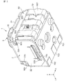
- FIG. 1 is a perspective view of a rotary encoder according to an embodiment of the present invention as viewed from above.
- FIG. 2 is a perspective view of the rotary encoder as viewed from below.
- FIG. 3 is an exploded perspective view of the rotary encoder as viewed from above.
- FIG. 4 is an exploded perspective view of the rotary encoder as viewed from below.
- FIG. 5 is a cross-sectional view of the rotary encoder.
- the width direction of the rotary encoder is the X direction
- the length direction of the rotary encoder is the Y direction
- the height direction of the rotary encoder is taken as the Z direction.
- the positive direction in the Z direction is the upper side
- the negative direction in the Z direction is the lower side.
- the rotary encoder 1 includes a casing 2, a shaft 3 having a rotation axis and movable along the rotation axis, and a regulating member 5 that regulates the rotation angle of the shaft 3.
- the encoder mechanism 6 detects the rotation direction and the rotation angle of the shaft 3, and the switch mechanism 7 is pressed against the shaft 3 by the movement along the rotation axis of the shaft 3.
- the restriction member 5, the encoder mechanism 6, and the switch mechanism 7 are arranged in order from the upper side to the lower side along the axis of the shaft 3.
- Casing 2 is made of metal, for example.
- the casing 2 integrally assembles the shaft 3, the regulating member 5, the encoder mechanism 6, and the switch mechanism 7.
- the casing 2 includes an upper wall 21, side walls 22, 22 provided on both sides of the upper wall 21 in the X direction and extending downward, and a protruding wall provided in the positive direction of the upper wall 21 in the Y direction and extending downward. 23 and a protruding piece 24 provided in the negative direction of the upper wall 21 in the Y direction and extending downward.
- the upper wall 21 has a hole 21a.
- the side wall 22 has a hole 22a on the lower side and a groove 22b on the upper side.
- On the inner surface of the hole 22a, a locking portion 22c that protrudes inside the casing 2 is provided.
- the protruding wall 23 extends over the entire length of the upper wall 21 in the X direction.
- the projecting piece 24 is provided at the center of the upper wall 21 in the X direction.
- the shaft 3 is made of, for example, resin.
- the shaft 3 includes an operation portion 35, a gear-shaped outer peripheral surface 30, and an end portion 36.
- the operation part 35, the gear-shaped outer peripheral surface 30, and the end part 36 are arranged in order from the upper side to the lower side along the rotation axis.
- the operation unit 35 has a notch that serves as a mark for the rotation of the shaft 3.
- the gear-shaped outer peripheral surface 30 includes a plurality of convex portions 31 and concave portions 32.
- the plurality of convex portions 31 and concave portions 32 are alternately arranged in the circumferential direction.
- the operation unit 35 penetrates the hole 21 a of the upper wall 21 of the casing 2, and the user can operate the operation unit 35 from the outside of the casing 2.
- the regulating member 5 is made of metal, for example.
- the regulating member 5 is a leaf spring, for example.
- the regulating member 5 has a first contact portion 51 and a second contact portion 52 that can come into contact with the outer peripheral surface 30 of the shaft 3.
- the first contact portion 51 and the second contact portion 52 are elastically biased to contact the convex portion 31 of the outer peripheral surface 30 of the shaft 3, while being fitted in the concave portion 32 of the outer peripheral surface 30 of the shaft 3. Regulate the rotation angle.
- the first contact portion 51 and the second contact portion 52 are configured to be bent.
- the 1st contact part 51 and the 2nd contact part 52 exist in the position which opposes substantially.
- the encoder mechanism 6 holds the shaft 3 in an inserted state so as to be rotatable and vertically movable, and detects the rotation direction and rotation angle of the shaft 3, and includes the resistor portions 61, 62, 63 and the resistor portion 61. , 62, 63, a substrate 60 having encoder terminals 601, 602, 603, a rotor 65 attached to the shaft 3 so as to be rotatable together with the shaft 3, and a resistor attached to the rotor 65. It has the slider 66 which slidably contacts the parts 61, 62, and 63.
- the substrate 60 is made of, for example, resin.
- a recess 60a is provided on the upper surface of the substrate 60, and the regulating member 5 is fitted in the recess 60a.
- Protrusions 60 b are provided on both sides of the substrate 60 in the X direction.
- the protrusion 60 b is fitted in the groove 22 b of the side wall 22 of the casing 2. Both sides of the substrate 60 in the Y direction are sandwiched between the protruding wall 23 and the protruding piece 24.
- the substrate 60 is fixed to the casing 2 by the groove portion 22 b of the side wall 22, the protruding wall 23, and the protruding piece 24.
- the groove portion 22 b of the side wall 22, the protruding wall 23, and the protruding piece 24 constitute an encoder fixing portion that fixes the substrate 60.
- a hole 64 serving as an insertion hole for holding the shaft 3 in an inserted state is formed in the center of the substrate 60.
- the resistor portions 61, 62, and 63 are provided on the lower surface of the substrate 60.
- the resistor portions 61, 62, and 63 are for detecting the rotation direction and rotation angle of the shaft 3.
- the first resistor part 61, the second resistor part 62, and the third resistor part 63 are formed in an annular shape and are arranged concentrically.
- the 1st resistor part 61, the 2nd resistor part 62, and the 3rd resistor part 63 are arrange
- the first resistor portion 61 and the second resistor portion 62 are each formed with an interval in the circumferential direction.
- the third resistor part 63 is formed continuously.
- Encoder terminals 601, 602, and 603 are insert-molded on the substrate 60.
- the first encoder terminal 601 is electrically connected to the first resistor part 61
- the second encoder terminal 602 is electrically connected to the second resistor part 62
- the third encoder terminal 603 is a third resistor. It is electrically connected to the body part 63.
- the rotor 65 only needs to be rotatable integrally with the shaft 3, and may or may not be movable in the axial direction.
- the rotor 65 is positioned in the circumferential direction with respect to the shaft 3 and is movable in the axial direction (upper limit movable). More specifically, the rotor 65 has a D-shaped hole 65a.
- the outer peripheral surface of the end portion 36 of the shaft 3 is formed in a D shape.
- the D-shaped end portion 36 is fitted into the D-shaped hole 65a, so that the rotor 65 is fixed to the shaft 3 in the circumferential direction and is not fixed in the axial direction.
- the rotor 65 is formed in a substantially oval shape.
- the rotor 65 has a long diameter portion 651 in which the outer diameter of the rotor 65 is a long diameter, and a short diameter portion 652 in which the outer diameter of the rotor 65 is a short diameter.
- the length of the long diameter portion 651 is larger than the gap between the locking portions 22c of the opposite side walls 22, and the length of the short diameter portion 652 is smaller than the gap between the locking portions 22c of the opposite side walls 22.
- the locking portion 22 c is configured such that the short diameter portion 652 is detached without locking and the long diameter portion 651 can be engaged and disengaged by the rotation of the rotor 65.
- the slider 66 is made of metal, for example.
- the slider 66 is fixed to the two protrusions 65 b on the upper surface of the rotor 65.
- the slider 66 is formed in an annular shape.
- the slider 66 has a first contact portion 661, a second contact portion 662, and a third contact portion 663.
- the first contact portion 661, the second contact portion 662, and the third contact portion 663 are sequentially arranged from the outer side to the inner side in the radial direction.
- the first contact part 661, the second contact part 662, and the third contact part 663 are electrically connected.
- the first contact portion 661 can come into contact with the first resistor portion 61
- the second contact portion 662 can come into contact with the second resistor portion 62
- the third contact portion 663 comes into contact with the third resistor portion 63. It becomes possible to contact.
- the switch mechanism 7 includes a switch board 70, first to third switch terminals 701, 702, and 703 provided on the switch board 70, and a conductor provided on the switch board 70 and pressed against the end portion 36 of the shaft 3. 71.
- the conductor 71 is electrically connected to the first and second switch terminals 701 and 702.
- the conductor 71 is pressed by the end portion 36 of the shaft 3 and is electrically connected to the third switch terminal 703 to conduct the first and second switch terminals 701 and 702 and the third switch terminal 703.
- the switch signal is turned on.
- each function operates when the switch signal is turned on. Note that only one of the first and second switch terminals 701 and 702 may be provided.
- Projections 70b are provided on both sides of the switch board 70 in the X direction.
- the protrusion 70 b is fitted in the hole 22 a of the side wall 22 of the casing 2.
- the switch board 70 is fixed to the casing 2 by the hole 22 a of the side wall 22.
- the hole 22 a of the side wall 22 constitutes a switch fixing portion that fixes the switch substrate 70.
- a stepped portion 70c is provided on one side of the lower surface of the switch substrate 70 in the X direction. End portions of the bent encoder terminals 601, 602, and 603 are locked to the stepped portion 70c. That is, the substrate 60 and the switch substrate 70 are held together by the bent encoder terminals 601, 602, and 603.
- the depth of the stepped portion 70c is deeper than the thickness of the encoder terminals 601, 602, 603.
- the first to third switch terminals 701, 702, and 703 are insert-molded on the switch board 70.
- the third switch terminal 703 is located between the first switch terminal 701 and the second switch terminal 702.
- the conductor 71 has elasticity.
- the conductor 71 is formed in a dome shape.
- the conductor 71 is fitted in the recess 70 a on the upper surface of the switch substrate 70.
- the peripheral portion 71 a of the conductor 71 is electrically connected to the first and second switch terminals 701 and 702.
- the zenith portion 71 b of the conductor 71 is separated from the third switch terminal 703 in the free state of the conductor 71, while being pressed by the end portion 36 of the shaft 3 penetrating the encoder mechanism 6 and electrically connected to the third switch terminal 703. Connected.
- the end portion 36 of the shaft 3 presses the zenith portion 71 b of the conductor 71, and the zenith portion 71 b of the conductor 71 is electrically connected to the third switch terminal 703. Is done.
- the first and second switch terminals 701 and 702 and the third switch terminal 703 are electrically connected, and the switch signal is turned on.
- the conductor 71 returns to the free state, so that the shaft 3 moves upward, and the zenith portion 71b of the conductor 71 is separated from the third switch terminal 703. .
- the first and second switch terminals 701 and 702 and the third switch terminal 703 are not electrically connected, and the switch signal is turned off.
- the slider 66 is located closer to the switch mechanism 7 (lower side) than the resistor portions 61, 62, 63. Thereby, when the shaft 3 is pressed to the switch mechanism 7 side, even if the rotor 65 is pulled downward, the slider 66 receives a force in a direction away from the resistor portions 61, 62, 63. For this reason, the slider 66 is not pressed and deformed by the resistor portions 61, 62, 63, and the output reliability of the encoder mechanism 6 can be maintained.
- FIG. 6 is an exploded perspective view of the encoder mechanism 6 as viewed from below.
- first, second, and third electrode portions 671, 672, and 673 are provided on the lower surface of the substrate 60.
- the 1st electrode part 671, the 2nd electrode part 672, and the 3rd electrode part 673 are formed in an annular shape, and are arranged concentrically.
- the 1st electrode part 671, the 2nd electrode part 672, and the 3rd electrode part 673 are arranged in order from the outside in the diameter direction to the inside.
- the first electrode portion 671 is electrically connected to the end portion 601a of the first encoder terminal 601
- the second electrode portion 672 is electrically connected to the end portion 602a of the second encoder terminal 602
- the third electrode portion. 673 is electrically connected to the end 603a of the third encoder terminal 603.
- an insulator portion 68 is laminated on the first, second, and third electrode portions 671, 672, and 673.
- the insulator portion 68 includes the first electrode portion 671 and the second electrode portion so that the first electrode portion 671 is intermittently exposed in the circumferential direction and the second electrode portion 672 is intermittently exposed in the circumferential direction. 672 is covered. That is, the insulator part 68 has a plurality of holes 68 a that are intermittently arranged in the circumferential direction, and the first electrode part 671 and the second electrode part 672 are exposed from the hole part 68 a of the insulator part 68. To do.
- the third electrode part 673 is not covered with the insulator part 68.
- the first resistor portion 61 is provided in a portion where the first electrode portion 671 is exposed from the insulator portion 68, and the second resistor portion 62 is provided in a portion where the second electrode portion 672 is exposed from the insulator portion 68.
- the third resistor part 63 is provided on the third electrode part 673.
- the first resistor portion 61 is electrically connected to the first encoder terminal 601 via the first electrode portion 671
- the second resistor portion 62 is connected to the first electrode portion 672 via the second electrode portion 672.
- 2 is electrically connected to the encoder terminal 602
- the third resistor part 63 is electrically connected to the third encoder terminal 603 via the third electrode part 673.
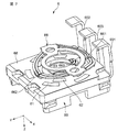
- FIG. 7 is a perspective view of the encoder mechanism 6 as viewed from below. As shown in FIG. 7, the first contact portion 661 of the slider 66 is in a position corresponding to the first resistor portion 61, and the second contact portion 662 of the slider 66 is the second resistor portion 62. The third contact portion 663 of the slider 66 is at a position corresponding to the third resistor portion 63.
- the slider 66 is in sliding contact with the insulator portion 68 and the resistor portions 61 and 62 alternately by the rotation of the shaft 3. Specifically, by rotating the shaft 3, the first contact portions 661 of the slider 66 are alternately in contact with the first resistor portions 61 and the insulator portions 68, and the second contact portions 662 are The second resistor portion 62 and the insulator portion 68 are alternately contacted.
- the third contact part 663 is always in contact with the third resistor part 63. That is, by the rotation of the slider 66, the first encoder terminal 601 and the third encoder terminal 603 are intermittently electrically connected, and the second encoder terminal 602 and the third encoder terminal 603 are intermittently connected. Electrically connected.
- the slider 66 is disposed so as to be positioned closer to the switch mechanism 7 than the insulator portion 68 and the resistor portions 61 and 62. Thereby, even if the shaft 3 is pressed, the slider 66 is not pressed against the insulator portion 68 and the resistor portions 61 and 62, and between the slider 66 and the insulator portion 68 and the resistor portions 61 and 62. Therefore, the wear of the insulator 68 and the wear of the slider 66 can be reduced.
- FIG. 8 is a schematic cross-sectional view of the insulator 68.
- the internal state of the insulator portion 68 is schematically illustrated for easy understanding.
- the insulator portion 68 includes a base material 10 made of resin, spherical silica 8, and a fluorine-based resin filler 9.
- a plurality of spherical silicas 8 and fluorine-based resin fillers 9 are present in the base material 10.
- the plurality of spherical silica 8 and the fluorine-based resin filler 9 exist between one surface 681 facing the slider of the insulator part 68 and the other surface 682 facing the substrate of the insulator part 68.
- the hardness of the spherical silica 8 is larger than that of the base material 10 and is equal to or higher than that of metal. Therefore, when the insulator 68 includes the spherical silica 8, the insulator 66 has a high hardness due to the high hardness of the spherical silica 8 included in the insulator 68 when the slider 66 slides on the insulator 68. Wear can be reduced. Specifically, when the contact portions 661 and 662 slide on one surface 681 of the insulator portion 68, the displacement of the insulator portion 68 due to the contact portions 661 and 662 can be reduced.
- the spherical silica 8 has a spherical shape having a cross section without a corner such as a perfect circle or an ellipse.
- a spherical silica 8 having no sharpness, the unevenness of the one surface 681 of the insulator portion 68 can be reduced, and the sliding of the slider 66 is improved, so that the wear of the slider 66 can be reduced. it can.
- the contact parts 661 and 662 slide on the one surface 681 of the insulator part 68, the sliding of the slider 66 is improved, so that the wear of the slider 66 by the contact parts 661 and 662 is reduced. Can do.
- the friction coefficient of the fluororesin filler 9 is smaller than that of the spherical silica 8 or the base material 10. For this reason, since the insulator part 68 contains the fluororesin filler 9, the frictional resistance between the slider 66 and the insulator part 68 is reduced, so that the wear of the slider 66 can be reduced. . Specifically, when the contact portions 661 and 662 slide on one surface 681 facing the slider of the insulator portion 68, the frictional resistance between the contact portions 661 and 662 and the insulator portion 68 becomes small. The wear of the slider 66 due to the contact portions 661 and 662 can be reduced.
- the average particle diameter of the spherical silica 8 contained in the insulator part 68 is 0.4 ⁇ m or more and 0.8 ⁇ m or less, preferably 0.5 ⁇ m or more and 0.7 ⁇ m or less.
- the unevenness of the one surface 681 of the insulator part 68 can be reduced, more specifically, to 10 ⁇ m or less (described in the examples). Thereby, the contact failure that the slider 66 contacts the insulator portion 68 but does not contact the resistor portions 61 and 62 is improved, and the reliability of the output of the encoder mechanism 6 can be improved.
- the moldability of the insulating material containing the spherical silica 8 can be maintained to the extent that the insulator portion 68 can be molded.
- the one surface 681 side of the insulator portion 68 has less spherical silica 8 and more fluorine resin filler 9 than the other surface 682 side of the insulator portion 68. Since the fluorine resin filler 9 is contained in a large amount on the one surface 681 side of the insulator portion 68, the frictional resistance between the slider 66 and the insulator portion 68 is reduced, so that the wear of the slider 66 is reduced. be able to. Specifically, the frictional resistance between the contact portions 661 and 662 and the insulator portion 68 when the contact portions 661 and 662 slide on one surface 681 facing the slider of the insulator portion 68 is reduced. Therefore, the wear of the slider 66 by the contact portions 661 and 662 can be reduced.
- the content of the spherical silica 8 contained in the insulator 68 is 5 vol% or more and 50 vol% or less, preferably 25 vol% or more, preferably 40 vol% or less, and the content of the fluororesin filler 9 is 1 vol% or more and 20 vol% or less, Preferably, it is 3 vol% or more and 8 vol% or less, and the sum of the content of the spherical silica 8 and the content of the fluororesin filler 9 is 50 vol% or less, preferably 48 vol% or less.
- the contents of the spherical silica 8 and the fluorine resin filler 9 it is possible to effectively reduce both the wear of the insulator portion 68 and the wear of the slider 66. Specifically, it is described in the examples.
- the average particle diameter of the fluororesin filler 9 contained in the insulator part 68 is 50 nm to 800 nm, preferably 50 nm to 300 nm.
- the fluororesin filler 9 contained in the insulator part 68 is polytetrafluoroethylene, and thereby, the insulator part 68 having good slidability and less frictional heat deformation can be configured.
- tetrafluoroethylene / perfluoroalkyl vinyl ether copolymer (PFA), polychlorotrifluoroethylene (PCTFE), tetrafluoroethylene / hexafluoropropylene copolymer (FEP), polyvinylidene fluoride (PVDF), tetra Fluoroethylene / ethylene copolymer (ETFE), polyvinyl fluoride (PVF), or the like can be used instead of polytetrafluoroethylene.
- the base material 10 included in the insulator 68 is an epoxy resin. Since the epoxy resin is a material that does not easily generate wear powder due to wear, the wear powder generated when the slider 66 is in sliding contact with the insulator 68 can be reduced by using the base material 10 as an epoxy resin. Encoder performance can be improved and service life can be extended. Also, for example, thermosetting resins such as urethane resin, polyimide resin, silicone resin, fluorine resin, liquid crystal polymer resin, polyphenyl sulfide resin, polyethylene, polypropylene, polyvinyl chloride, polystyrene, polyvinyl acetate, acrylic, polyester, etc. A thermoplastic resin can be used in place of the epoxy resin.
- thermosetting resins such as urethane resin, polyimide resin, silicone resin, fluorine resin, liquid crystal polymer resin, polyphenyl sulfide resin, polyethylene, polypropylene, polyvinyl chloride, polystyrene, polyvinyl acetate
- An insulating material including a base material 10 made of resin, spherical silica 8 and fluorine resin filler 9 is prepared.
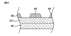
- electrode portions 671 and 672 are provided on one surface of the substrate 60 so as to extend in the rotation direction of the shaft 3, and the prepared insulating material is intermittently provided in the circumferential direction of the electrode portions 671 and 672.
- An insulator is formed on the electrode portion so as to be exposed.
- the insulating material 68 is formed by applying an insulating material by screen printing using a mask and curing the applied insulating material.
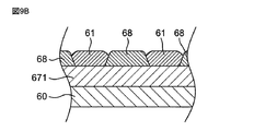
- the resistor portions 61 and 62 are formed by applying a resistor material on the electrode portions 671 and 672 exposed from the insulator portion 68. Specifically, the resistor portions 61 and 62 are formed by applying a resistor material by screen printing using a mask and curing the applied resistor material. By manufacturing in this way, it is possible to manufacture a rotary encoder in which both the wear of the insulating substrate and the wear of the slider are reduced.
- the second fluororesin filler 9 (hereinafter referred to as secondary particle fluororesin filler 9), the spherical silica 8 and the base material 10 are kneaded,
- a first fluorine resin filler 9 (hereinafter referred to as primary particle fluorine resin filler 9) is produced by crushing the fluorine resin filler 9 of secondary particles.
- the average particle size of the fluororesin filler 9 of the secondary particles used is 0.5 ⁇ m or more and 10 ⁇ m or less, preferably 2 ⁇ m or more and 8 ⁇ m or less.
- the average particle size of the pulverized primary resin fluorine-based resin filler 9 is 50 nm to 800 nm, preferably 50 nm to 300 nm.
- the spherical silica 8 having a higher hardness serves as a grinding medium, and the secondary particles are effectively used. Can be crushed. Thereby, the insulating material containing the fluorine resin filler 9 with a small average particle diameter is obtained. When the obtained insulating material is applied onto the electrode portions 671 and 672, the spherical silica 8 having a large particle size settles at a higher speed than the fluorine resin filler 9 having a smaller particle size in accordance with the Stokes equation.
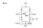
- FIG. 10 is a circuit diagram showing an equivalent circuit of the encoder mechanism 6.
- FIG. 11 is a waveform diagram showing an output waveform of the encoder mechanism 6.
- a current flows between the points A and C, and the A signal is turned on.
- the second encoder terminal 602 and the third encoder terminal 603 are electrically connected, a current flows between point B and point C, and the B signal is turned on.
- the rotation angle of the slider 66 from the start of turning off the A signal to the start of the next off is 60 °.
- the difference between the start of turning off the A signal and the start of turning off the B signal is 15 ° in the rotation angle of the slider 66.
- the change in the combination of ON and OFF of the A signal and the B signal is divided into 24. That is, it can be determined that the rotation angle of the slider 66 changes every 15 ° in one rotation of the slider 66. Therefore, the rotation direction and rotation angle (rotation amount) of the slider 66 can be determined by determining changes in the A signal and the B signal.
- FIG. 12 is a plan view showing the relationship between the shaft 3 and the regulating member 5.
- the second contact portion 52 of the restriction member 5 is It fits into the recess 32 of the outer peripheral surface 30.
- the first contact portion 51 of the regulating member 5 is fitted in the concave portion 32 of the outer peripheral surface 30 of the shaft 3
- the second contact portion 52 of the regulating member 5 is the convex portion of the outer peripheral surface 30 of the shaft 3. 31 is contacted.
- the phase difference of the rotation angle of the shaft 3 is provided between the contact between the first contact portion 51 and the convex portion 31 and the contact between the second contact portion 52 and the convex portion 31. And if the shaft 3 rotates, the 1st contact part 51 and the 2nd contact part 52 will fit in the recessed part 32 of the outer peripheral surface 30 of the shaft 3 by turns.
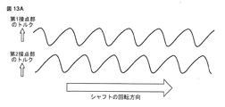
- FIG. 13A is a graph showing changes in torque of the first contact portion 51 and the second contact portion 52 when the shaft 3 rotates.
- each torque of the first contact portion 51 and the second contact portion 52 has a waveform that repeats maximum and minimum.
- the torque becomes maximum when the convex portion 31 of the outer peripheral surface 30 of the shaft 3 passes against the elastic force of the first contact portion 51 due to the rotation of the shaft 3.
- the user gets a click when the torque is from maximum to minimum.
- the torque of the first contact portion 51 and the torque of the second contact portion 52 are alternately maximum.
- FIG. 13B is a graph showing a change in torque obtained by combining the torque of the first contact portion 51 and the torque of the second contact portion 52.
- the wavelength of the waveform of the combined torque is twice the wavelength of the torque waveform of the first contact portion 51 and the second contact portion 52. That is, in one rotation of the shaft 3, the quantity (number of clicks) that maximizes the combined torque is the quantity (number of clicks) that maximizes the torque of the first contact part 51 and the torque of the second contact part 52 is maximum. It becomes the quantity which added the quantity (number of clicks).
- the total number of clicks is 2 of the number of clicks of the first contact portion 51 and the second contact portion 52. Doubled. Therefore, even if the shaft 3 is downsized, the number of clicks can be increased.
- Example 1 A test for evaluating the wear resistance of the insulator and the slider when the rotary encoder described in the above embodiment was used was performed.
- the method for evaluating the wear resistance of the insulator is as follows. As shown in Table 1, the type of the insulator part 68 was changed, and the slider 66 was rotated 300,000 times while alternately sliding on the surface of the insulator part 68 and the surface of the first resistor part 61. At this time, wear marks were generated on one surface 681 of the insulator 68 due to repeated sliding of the slider 66. Five points are arbitrarily selected from the areas of the generated wear traces, and the depth ( ⁇ m) from the area where the wear marks of the one surface 681 of the insulator portion 68 are not generated is measured for each point, and the average of the five depths is measured. The value was defined as the amount of wear on the insulator of the rotary encoder 1.
- the two protrusions of the contact portions 661 and 662 of the slider 66 are worn by alternately slidingly contacting the first resistor portion 61 and the insulator portion 68, Wear planes S1 and S2 were formed.
- the wear planes S1 and S2 of the contact portions 661 and 662 of the slider 66 are indicated by hatched portions in FIG.
- the areas of the formed wear planes S1 and S2 were measured, and the average value of the two areas was defined as the slider wear area of the rotary encoder 1.
- the average particle diameter of the spherical silica 8 used for the insulator part 68 was 0.6 ⁇ m.
- the average particle diameter is determined from the particle diameter measured by laser diffraction (Horiba Microtrac) after ultrasonically dispersing the particles in an aqueous solution of sodium hexametaphosphate.
- Comparative Example 8 using molybdenum disulfide MoS 2 instead of PTFE as the fluororesin filler 9, the insulator part 68 contains spherical silica 8, so that the insulator part 68 does not contain spherical silica 8 (Comparative Example). Although the amount of wear of the insulator portion was reduced as compared with 1), the wear area of the slider greatly exceeded 10,000 ⁇ m 2 . In Comparative Example 9 in which the insulating material does not contain spherical silica 8 and contains only calcium carbonate (CaCO 3 ), the amount of wear on the insulator is larger than in other Examples and Comparative Examples using silica, and the slider The wear area exceeded 20,000 ⁇ m 2 .
- the specific weight (weight per volume) of silica, filler and base material is used to obtain the desired content.
- the volume% of each material was converted to weight%, and each material was weighed based on the converted weight% of each material to prepare an insulating material.
- Example 2 Next, a test was conducted to examine the relationship between the average particle diameter of the spherical silica 8 to be used and the surface irregularities of the insulator portion 68.
- the test method is as follows.
- the insulating material is adjusted by kneading the spherical silica 8, the secondary particle PTFE, and the base material 10 so as to crush the secondary particle PTFE.
- PTFE is crushed to primary particles.
- the rotary encoder 1 described in the embodiment was manufactured, and the unevenness of one surface 681 facing the slider of the insulator portion 68 of the prepared rotary encoder 1 was measured.
- the maximum roughness Rz of the natural surface of the insulator portion 68 after being hard measured using a Keyence laser microscope is the unevenness of one surface 681 facing the slider (corresponding to the surface unevenness in Table 2). did.
- the test which measures the insulator part abrasion loss and the slider abrasion area with the method similar to Example 1 with respect to the produced rotary encoder 1 was done.
- the surface unevenness of the insulator portion 68 could be suppressed to within 10 ⁇ m (Example 1-3).
- the PTFE of the secondary particles was sufficiently crushed at the time of kneading with the spherical silica 8 and the base material 10 and was present as primary particles having an average particle size of less than 1 ⁇ m in the insulating material. It is considered that the surface unevenness of the surface was able to be suppressed within 10 ⁇ m.
Landscapes
- Physics & Mathematics (AREA)
- General Physics & Mathematics (AREA)
- Engineering & Computer Science (AREA)
- Manufacturing & Machinery (AREA)
- Transmission And Conversion Of Sensor Element Output (AREA)
- Rotary Switch, Piano Key Switch, And Lever Switch (AREA)
Abstract
回転エンコーダは、シャフトと、前記シャフトを回転可能に挿通状態で保持するとともに、前記シャフトの回転方向および回転角度を検知するエンコーダ機構とを有する。前記エンコーダ機構は、前記シャフトを回転可能に保持する基板と、前記基板の一面に設けられ、前記シャフトの回転方向に交互に設けられた絶縁体部および抵抗体部と、前記シャフトと一体的に回転可能に前記シャフトに取り付けられたロータと、該ロータに取り付けられ、前記シャフトの回転により、該絶縁体部と該抵抗体部に交互に摺接する摺動子とを有する。該絶縁体部は、樹脂からなる母材と、球状シリカと、フッ素系樹脂フィラーとを含む。
Description
本発明は、回転エンコーダに関する。
従来、回転エンコーダとしては、例えば、特開平1-258328号公報(特許文献1)に記載されたものがある。特許文献1の回転エンコーダは、シャフトと、樹脂からなる絶縁基板と、絶縁基板の一面にシャフトの回転方向に間欠的に形成された電極パターンと、シャフトと共に回転可能に構成され、シャフトの回転により絶縁基板と電極パターンとに交互に摺接する金属製の摺動子とを有している。
ところで、従来の回転エンコーダでは、絶縁基板が樹脂からなるため、絶縁基板の硬度が摺動子の硬度よりも低くなり、摺動子が絶縁基板上を摺動する際に、絶縁基板が摩耗するという問題があった。
そこで、本発明は上記課題を解決するためになされたものであって、絶縁基板の摩耗を低減することができる回転エンコーダを提供することを目的とする。
前記の課題を解決するため、本発明のある局面に係る回転エンコーダは、
シャフトと、
前記シャフトを回転可能に挿通状態で保持するとともに、前記シャフトの回転方向および回転角度を検知するエンコーダ機構とを有し、
前記エンコーダ機構は、
前記シャフトを回転可能に保持する基板と、
前記基板の一面に設けられ、シャフトの回転方向に交互に設けられた絶縁体部および抵抗体部と、
前記シャフトと一体的に回転可能に前記シャフトに取り付けられたロータと、
該ロータに取り付けられ、前記シャフトの回転により、該絶縁体部と該抵抗体部に交互に摺接する摺動子とを有し、
該絶縁体部は、樹脂からなる母材と、球状シリカと、フッ素系樹脂フィラーとを含むことを特徴とする。
シャフトと、
前記シャフトを回転可能に挿通状態で保持するとともに、前記シャフトの回転方向および回転角度を検知するエンコーダ機構とを有し、
前記エンコーダ機構は、
前記シャフトを回転可能に保持する基板と、
前記基板の一面に設けられ、シャフトの回転方向に交互に設けられた絶縁体部および抵抗体部と、
前記シャフトと一体的に回転可能に前記シャフトに取り付けられたロータと、
該ロータに取り付けられ、前記シャフトの回転により、該絶縁体部と該抵抗体部に交互に摺接する摺動子とを有し、
該絶縁体部は、樹脂からなる母材と、球状シリカと、フッ素系樹脂フィラーとを含むことを特徴とする。
本発明のある局面に係る回転エンコーダによれば、摺動子が絶縁体部を摺動する際に、絶縁体部に含まれる球状シリカの高い硬度により、絶縁体部の摩耗を低減することができる。また、絶縁体部の球状シリカの尖りがない形状により、絶縁体部の摺動子が摺動する一面における摺動子の滑りがよく、かつ、絶縁体部のフッ素系樹脂フィラーにより摩擦係数が低減され、この結果、摺動子の摩耗を低減することができる。したがって、絶縁基板の摩耗と、摺動子の摩耗の両方を低減することができる。
また、一実施形態の回転エンコーダでは、前記球状シリカの平均粒径は0.4μm以上0.8μm以下である。
本明細書において平均粒径とは、体積基準で粒度分布を求め、全体積を100%とした累積曲線において、累積値が50%となる点の粒径(D50)である。かかる平均粒径は、レーザー回折・散乱式 粒子径・粒度分布測定装置または電子走査顕微鏡を用いて測定することができる。
前記実施形態の回転エンコーダによれば、球状シリカの平均粒径が小さいので、絶縁体部の表面凹凸を小さく抑えることができ、絶縁体部の表面と、抵抗体部の表面との高さの差を小さくすることができる。これにより、摺動子が絶縁体部に接触するが抵抗体部に接触しないという接触不良を改善できる。
また、一実施形態の回転エンコーダでは、前記絶縁体部に含まれる前記球状シリカの含有率は5vol%以上50vol%以下であり、前記絶縁体部に含まれる前記フッ素系樹脂フィラーの含有率は1vol%以上20vol%以下であり、前記球状シリカの含有率と前記フッ素系樹脂フィラーの含有率の和は50vol%以下である。
前記実施形態の回転エンコーダによれば、絶縁体部の摩耗と摺動子の摩耗の両方の低減を効果的に実現できる。
また、一実施形態の回転エンコーダでは、前記フッ素系樹脂フィラーの平均粒径は50nm以上800nm以下である。
前記実施形態の回転エンコーダによれば、フッ素系樹脂フィラーの平均粒径が小さいため、フッ素系樹脂フィラーが絶縁体部の摺動子に接する表面側へ偏在できる。これにより、絶縁体部の表面の摩擦係数を小さくでき、摺動子の摩耗を効果的に低減することができる。
また、一実施形態の回転エンコーダでは、前記フッ素系樹脂フィラーはポリテトラフルオロエチレンである。
前記実施形態の回転エンコーダによれば、フッ素系樹脂フィラーが、摩擦係数が他のフッ素系樹脂よりも低い0.04以下であり、耐熱性及び化学安定性に優れるポリテトラフルオロエチレンであるため、絶縁体部の摺動性が向上し摩擦熱変形が少なくなる。
また、一実施形態の回転エンコーダでは、前記母材はエポキシ樹脂である。
前記実施形態の回転エンコーダによれば、前記母材にエポキシ樹脂を用いることで、摺動子が絶縁体部に摺接することで生じる摩耗粉を低減することができる。これにより、回転エンコーダの性能が向上し、使用寿命を延ばすことができる。
また、一実施形態の回転エンコーダでは、前記絶縁体部の摺動子に対向する一面側は、基板に対向する他面側に比べて球状シリカが少なく、かつ、フッ素系樹脂フィラーが多い。
前記実施形態の回転エンコーダによれば、絶縁体部の摺動子に対向する一面側は、絶縁体部の基板に対向する他面側に比べてフッ素系樹脂フィラーが多いので、摺動子の摩耗を効果的に低減することができる。また、絶縁体部の摺動子に対向する一面側は、基板に対向する他面側に比べて球状シリカが少ないので、一面の凹凸を小さく抑えることができ、摺動子が絶縁体部に接触するが抵抗体部に接触しないという接触不良が改善される。
また、一実施形態において、回転エンコーダは、前記エンコーダ機構に挿通された前記シャフトの端部により押圧されるスイッチ機構を有し、前記摺動子は前記絶縁体部および前記抵抗体部よりも前記スイッチ機構側に位置するように配置される。
前記実施形態の回転エンコーダによれば、摺動子は絶縁体部および抵抗体部よりもスイッチ機構側に位置するように配置されており、シャフトを押下した際に摺動子が絶縁体部および抵抗体部に押し付けられることがない。これにより、摺動子と絶縁体部および抵抗体部との間の摺動性がシャフトの押下により損なわれないため、絶縁体部の摩耗と摺動子の摩耗の両方の低減を効果的に達成できる。
また、一実施形態では、本発明の回転エンコーダのエンコーダ機構は、樹脂からなる母材と、球状シリカと、フッ素系樹脂フィラーとを含む絶縁材料を準備する工程と、シャフトの回転方向に延在するように基板の一面に電極部を設ける工程と、準備した前記絶縁材料を、前記電極部が周方向に間欠的に露出するように前記電極部上に塗布して絶縁体部を形成する工程と、前記絶縁体部から露出する前記電極部を覆うように抵抗体材料を塗布して、前記抵抗体部を形成する工程と、を備える方法により製造される。
前記実施形態によれば、絶縁基板の摩耗と摺動子の摩耗の両方が低減された回転エンコーダを製造することができる。
また、一実施形態では、前記絶縁体部を準備する工程において、平均粒径が0.5μm以上10μm以下である第二のフッ素系樹脂フィラーと、球状シリカと、母材とを混練して、該第二のフッ素系樹脂フィラーの解砕により平均粒径が50nm以上800nm以下である第一のフッ素系樹脂フィラーを作製することにより、前記絶縁材料が準備される。
前記実施形態によれば、フッ素系樹脂フィラーの二次粒子と、球状シリカとを混練して解砕することで、より硬度の高い球状シリカが粉砕媒体の役割を果たし、二次粒子を効果的に解砕することができる。これにより、平均粒径の小さいフッ素系樹脂フィラーが得られ、フッ素系樹脂フィラーが摺動子に対向する一面側に偏在することができ、摺動子の摩耗を低減することができる。
本発明によれば、絶縁体部の摩耗と摺動子の摩耗の両方が低減された回転エンコーダが提供される。
本願発明者は、絶縁基板を金属製の摺動子よりも硬度の大きな材料から構成して絶縁基板の摩耗を防ぐように検討した。しかしながら、単純に絶縁基板の硬度を向上させるだけでは、絶縁基板の代わりに摺動子が摩耗して電気特性が変化するという問題が明らかになった。本願発明者は、この現象を鋭意検討したところ、絶縁体部の硬度を向上させると共に絶縁体部の摺動子に対する滑りを実現するために、母材に球状シリカとフッ素系樹脂フィラーを添加することを見出した。これにより絶縁体部の摩耗を低減しつつ、摺動子の摩耗をも低減することが可能となった。
本発明は、本願発明者が独自に得た上記知見に基づいてなされたものである。
本発明は、本願発明者が独自に得た上記知見に基づいてなされたものである。
以下、本発明について図面を参照してより詳細に説明する。
(実施形態)
図1は、本発明の一実施形態の回転エンコーダの上方からみた斜視図である。図2は、回転エンコーダの下方からみた斜視図である。図3は、回転エンコーダの上方からみた分解斜視図である。図4は、回転エンコーダの下方からみた分解斜視図である。図5は、回転エンコーダの断面図である。
図1は、本発明の一実施形態の回転エンコーダの上方からみた斜視図である。図2は、回転エンコーダの下方からみた斜視図である。図3は、回転エンコーダの上方からみた分解斜視図である。図4は、回転エンコーダの下方からみた分解斜視図である。図5は、回転エンコーダの断面図である。
各図において、回転エンコーダの幅方向をX方向とし、回転エンコーダの長さ方向をY方向とする。回転エンコーダの高さ方向をZ方向とする。Z方向の正方向を上側とし、Z方向の負方向を下側とする。
図1から図5に示すように、回転エンコーダ1は、ケーシング2と、回転軸を有しかつ該回転軸に沿って移動可能なシャフト3と、シャフト3の回転角度を規制する規制部材5と、シャフト3の回転方向および回転角度を検知するエンコーダ機構6と、シャフト3の回転軸に沿った移動によりシャフト3に押圧されるスイッチ機構7とを有する。規制部材5とエンコーダ機構6とスイッチ機構7とは、シャフト3の軸に沿って、上側から下側に順に配置されている。
ケーシング2は、例えば、金属から構成される。ケーシング2は、シャフト3と規制部材5とエンコーダ機構6とスイッチ機構7とを一体に組み付ける。
ケーシング2は、上壁21と、上壁21のX方向の両側に設けられ下方に延在する側壁22,22と、上壁21のY方向の正方向に設けられ下方に延在する突壁23と、上壁21のY方向の負方向に設けられ下方に延在する突片24とを有する。上壁21は、孔部21aを有する。側壁22は、下側に孔部22aと上側に溝部22bとを有する。孔部22aの内面には、ケーシング2の内側に突出する係止部22cが設けられている。突壁23は、上壁21のX方向の全長にわたって延在している。突片24は、上壁21のX方向の中央部に設けられている。
シャフト3は、例えば、樹脂から構成される。シャフト3は、操作部35と歯車状の外周面30と端部36とを有する。操作部35と歯車状の外周面30と端部36とは、回転軸に沿って、上側から下側に順に配置されている。操作部35は、シャフト3の回転の目印となる切欠を有する。歯車状の外周面30は、複数の凸部31および凹部32を含む。複数の凸部31および凹部32は、周方向に交互に配列されている。操作部35は、ケーシング2の上壁21の孔部21aを貫通しており、使用者は、ケーシング2の外側から操作部35を操作することができる。
規制部材5は、例えば、金属から構成される。規制部材5は、例えば、板バネである。規制部材5は、シャフト3の外周面30に接触可能となる第1接点部51および第2接点部52を有する。第1接点部51および第2接点部52は、シャフト3の外周面30の凸部31に弾発付勢して接触する一方、シャフト3の外周面30の凹部32に嵌まってシャフト3の回転角度を規制する。第1接点部51および第2接点部52は、折り曲げられて構成されている。第1接点部51および第2接点部52は、ほぼ対向する位置にある。
エンコーダ機構6は、シャフト3を回転可能および上下移動可能に挿通状態で保持し、シャフト3の回転方向および回転角度を検知するものであり、抵抗体部61,62,63と該抵抗体部61,62,63に電気的に接続されるエンコーダ端子601,602,603を有する基板60と、シャフト3とともに回転可能となるようにシャフト3に取り付けられたロータ65と、ロータ65に取り付けられ抵抗体部61,62,63と摺接する摺動子66とを有する。
基板60は、例えば、樹脂から構成される。基板60の上面には、凹部60aが設けられ、凹部60aに、規制部材5が嵌め込まれている。基板60のX方向の両側には、突部60bが設けられている。突部60bは、ケーシング2の側壁22の溝部22bに嵌め込まれている。基板60のY方向の両側は、突壁23と突片24によって挟まれている。このように、基板60は、側壁22の溝部22bと突壁23と突片24とによって、ケーシング2に固定されている。言い換えると、側壁22の溝部22bと突壁23と突片24とは、基板60を固定するエンコーダ固定部を構成する。基板60の中央には、シャフト3を挿通状態で保持する挿通孔となる孔部64が形成されている。
抵抗体部61,62,63は、基板60の下面に設けられている。抵抗体部61,62,63は、シャフト3の回転方向および回転角度を検知するためのものである。第1抵抗体部61と第2抵抗体部62と第3抵抗体部63とは、環状に形成され、同心状に配置されている。第1抵抗体部61と第2抵抗体部62と第3抵抗体部63とは、径方向の外側から内側に順に配置されている。第1抵抗体部61と第2抵抗体部62とは、それぞれ、周方向に間隔を設けて形成されている。第3抵抗体部63は、連続的に形成されている。
エンコーダ端子601,602,603は、基板60にインサート成形されている。第1エンコーダ端子601は、第1抵抗体部61に電気的に接続され、第2エンコーダ端子602は、第2抵抗体部62に電気的に接続され、第3エンコーダ端子603は、第3抵抗体部63に電気的に接続されている。
ロータ65は、シャフト3と一体的に回転可能であればよく、軸方向に移動可能でも移動できなくてもよい。図では、ロータ65は、シャフト3に対して、周方向に位置決めされ、かつ、軸方向に移動可能(上限移動可能)である場合を示している。具体的に述べると、ロータ65は、D形状の孔部65aを有する。シャフト3の端部36の外周面は、D形状に形成されている。D形状の端部36が、D形状の孔部65aに嵌合されて、ロータ65は、シャフト3に対して周方向に固定され軸方向に固定されない。
ロータ65は、略長円形状に形成されている。ロータ65は、ロータ65の外径が長径となる長径部651と、ロータ65の外径が短径となる短径部652とを有する。長径部651の長さは、対向する側壁22の係止部22cの間の隙間よりも大きく、短径部652の長さは、対向する側壁22の係止部22cの間の隙間よりも小さい。言い換えると、係止部22cは、短径部652が係止しないで離脱され、かつ、長径部651がロータ65の回転により係脱可能となるように、構成されている。
摺動子66は、例えば、金属から構成される。摺動子66は、ロータ65の上面の2つの突部65bに固定される。摺動子66は、環状に形成される。摺動子66は、第1接点部661と第2接点部662と第3接点部663とを有する。第1接点部661と第2接点部662と第3接点部663とは、径方向の外側から内側に順に配置されている。第1接点部661と第2接点部662と第3接点部663とは、導通している。第1接点部661は、第1抵抗体部61に接触可能となり、第2接点部662は、第2抵抗体部62に接触可能となり、第3接点部663は、第3抵抗体部63に接触可能となる。
スイッチ機構7は、スイッチ基板70と、スイッチ基板70に設けられた第1から第3スイッチ端子701,702,703と、スイッチ基板70に設けられ、シャフト3の端部36に押圧される導電体71とを有する。導電体71は、第1、第2スイッチ端子701,702に電気的に接続される。導電体71は、シャフト3の端部36に押圧されて、第3スイッチ端子703に電気的に接続され、第1、第2スイッチ端子701,702と第3スイッチ端子703とを導通する。第1、第2スイッチ端子701,702と第3スイッチ端子703とが導通すると、スイッチ信号がオンとなる。例えば、スイッチ信号のオンにより、各機能が動作する。なお、第1、第2スイッチ端子701,702のうちの一方のスイッチ端子のみ設けてもよい。
スイッチ基板70のX方向の両側には、突部70bが設けられている。突部70bは、ケーシング2の側壁22の孔部22aに嵌め込まれている。このように、スイッチ基板70は、側壁22の孔部22aによって、ケーシング2に固定されている。言い換えると、側壁22の孔部22aは、スイッチ基板70を固定するスイッチ固定部を構成する。
スイッチ基板70の下面のX方向の一辺には、段部70cが設けられている。段部70cには、折り曲げられたエンコーダ端子601,602,603の端部が、係止している。つまり、基板60とスイッチ基板70とは、折り曲げられたエンコーダ端子601,602,603によって、一体に抱えられている。
段部70cの深さは、エンコーダ端子601,602,603の厚みよりも深い。これにより、スイッチ基板70の下面を実装基板に設置したとき、エンコーダ端子601,602,603でなく、スイッチ基板70の下面を設置面とできる。
第1から第3スイッチ端子701,702,703は、スイッチ基板70にインサート成形されている。第3スイッチ端子703は、第1スイッチ端子701と第2スイッチ端子702との間に、位置する。
導電体71は、弾性を有する。導電体71は、ドーム状に形成されている。導電体71は、スイッチ基板70の上面の凹部70aに嵌め込まれている。
導電体71の周縁部分71aは、第1、第2スイッチ端子701,702に電気的に接続されている。導電体71の天頂部分71bは、導電体71の自由状態で、第3スイッチ端子703から離隔する一方、エンコーダ機構6を貫通したシャフト3の端部36に押圧されて第3スイッチ端子703に電気的に接続される。
つまり、シャフト3を下側に押圧すると、シャフト3の端部36が、導電体71の天頂部分71bを押圧して、導電体71の天頂部分71bが、第3スイッチ端子703に電気的に接続される。これにより、第1、第2スイッチ端子701,702と第3スイッチ端子703とが、電気的に接続されて、スイッチ信号がオンとなる。
一方、シャフト3の下側への押圧を解除すると、導電体71が自由状態に戻ることで、シャフト3が上側に移動し、導電体71の天頂部分71bが、第3スイッチ端子703から離隔する。これにより、第1、第2スイッチ端子701,702と第3スイッチ端子703とが、電気的に接続されず、スイッチ信号がオフとなる。
ここで、摺動子66は、抵抗体部61,62,63よりも、スイッチ機構7側(下側)に位置している。これにより、シャフト3をスイッチ機構7側に押圧したとき、ロータ65が下側に引っ張られても、摺動子66は、抵抗体部61,62,63から離れる方向に力を受ける。このため、摺動子66は、抵抗体部61,62,63に押圧されて変形することがなく、エンコーダ機構6の出力の信頼性を維持できる。さらに、シャフト3をロータ65に対して上下方向に移動可能とすることで、シャフト3を押圧しても、ロータ65の位置を保持して、摺動子66と抵抗体部61,62,63との接触を維持することができる。
図6は、エンコーダ機構6の下方からみた分解斜視図である。図6に示すように、基板60の下面には、第1、第2、第3電極部671,672,673が設けられている。第1電極部671と第2電極部672と第3電極部673とは、環状に形成され、同心状に配置されている。第1電極部671と第2電極部672と第3電極部673とは、径方向の外側から内側に順に配置されている。第1電極部671は、第1エンコーダ端子601の端部601aに電気的に接続され、第2電極部672は、第2エンコーダ端子602の端部602aに電気的に接続され、第3電極部673は、第3エンコーダ端子603の端部603aに電気的に接続されている。
第1、第2、第3電極部671,672,673上には、絶縁体部68が積層されている。絶縁体部68は、第1電極部671が周方向に間欠的に露出し、かつ、第2電極部672が周方向に間欠的に露出するように、第1電極部671および第2電極部672を覆う。つまり、絶縁体部68は、周方向に間欠的に配置される複数の孔部68aを有し、第1電極部671および第2電極部672が、絶縁体部68の孔部68aから、露出する。第3電極部673は、絶縁体部68に覆われていない。
第1電極部671が絶縁体部68から露出している部分に第1抵抗体部61を設け、第2電極部672が絶縁体部68から露出している部分に第2抵抗体部62を設け、第3電極部673に第3抵抗体部63を設けている。
これにより、第1抵抗体部61は、第1電極部671を介して、第1エンコーダ端子601に電気的に接続され、第2抵抗体部62は、第2電極部672を介して、第2エンコーダ端子602に電気的に接続され、第3抵抗体部63は、第3電極部673を介して、第3エンコーダ端子603に電気的に接続される。
図7は、エンコーダ機構6の下方からみた斜視図である。図7に示すように、摺動子66の第1接点部661は、第1抵抗体部61に対応した位置にあり、摺動子66の第2接点部662は、第2抵抗体部62に対応した位置にあり、摺動子66の第3接点部663は、第3抵抗体部63に対応した位置にある。
そして、摺動子66はシャフト3の回転により、絶縁体部68と抵抗体部61、62に交互に摺接する。具体的には、シャフト3を回転させることにより、摺動子66の第1接点部661は、第1抵抗体部61と絶縁体部68とに交互に接触し、第2接点部662は、第2抵抗体部62と絶縁体部68とに交互に接触する。第3接点部663は、常時、第3抵抗体部63に接触している。つまり、摺動子66の回転により、第1エンコーダ端子601と第3エンコーダ端子603とが、間欠的に電気的に接続され、第2エンコーダ端子602と第3エンコーダ端子603とが、間欠的に電気的に接続される。
図4に示すように、摺動子66は絶縁体部68および抵抗体部61、62よりもスイッチ機構7側に位置するように配置される。これにより、シャフト3を押下しても摺動子66が絶縁体部68および抵抗体部61、62に押し付けられず、摺動子66と絶縁体部68および抵抗体部61、62との間の摺動性がシャフト3の押下により損なわれなくなるため、絶縁体部68の摩耗と摺動子66の摩耗の両方の低減を実現することができる。
図8は、絶縁体部68の模式断面図である。図8では、絶縁体部68の内部の状態の特徴を分かりやすくするために模式的に描いている。図8に示すように、絶縁体部68は、樹脂からなる母材10と、球状シリカ8と、フッ素系樹脂フィラー9とを含む。球状シリカ8とフッ素系樹脂フィラー9はそれぞれ、母材10内に複数存在している。複数の球状シリカ8とフッ素系樹脂フィラー9は、絶縁体部68の摺動子に対向する一面681と、絶縁体部68の基板に対向する他面682との間に存在している。
球状シリカ8の硬度は母材10よりも大きく、金属と同等またはそれ以上である。したがって、絶縁体部68が球状シリカ8を含むことにより、摺動子66が絶縁体部68を摺動する際に、絶縁体部68に含まれる球状シリカ8の高い硬度により、絶縁体部68の摩耗を低減することができる。具体的には、接点部661、662が絶縁体部68の一面681を摺動する際に、接点部661、662による絶縁体部68のけずれを低減することができる。
球状シリカ8は、真円または楕円などの角のない断面を有する球状の形状を有する。このような、尖りがない球状シリカ8を使用することで、絶縁体部68の一面681の凹凸を少なくでき、摺動子66の滑りがよくなるため、摺動子66の摩耗を低減することができる。具体的には、接点部661、662が絶縁体部68の一面681を摺動する際、摺動子66の滑りがよくなるため、接点部661、662による摺動子66のすり減りを低減することができる。
フッ素系樹脂フィラー9の摩擦係数は、球状シリカ8や母材10より小さい。このため、絶縁体部68がフッ素系樹脂フィラー9を含むことにより、摺動子66と絶縁体部68との間の摩擦抵抗が小さくなるため、摺動子66の摩耗を低減することができる。具体的には、接点部661、662が絶縁体部68の摺動子に対向する一面681を摺動する際、接点部661、662と絶縁体部68との間の摩擦抵抗が小さくなるため、接点部661、662による摺動子66のすり減りを低減することができる。
絶縁体部68に含まれる球状シリカ8の平均粒径は0.4μm以上0.8μm以下、好ましくは0.5μm以上0.7μm以下である。球状シリカ8の平均粒径を0.8μm以下とすることで、絶縁体部68の一面681の凹凸を小さく、より詳細には10μm以下(実施例に記載)に抑えることができる。これにより、摺動子66が絶縁体部68に接触するが抵抗体部61、62に接触しないという接触不良が改善され、エンコーダ機構6の出力の信頼性を高めることができる。また、球状シリカ8の平均粒径を0.4μm以上とすることで、球状シリカ8を含む絶縁材料の成型性を、絶縁体部68を成形可能な程度に維持することができる。
絶縁体部68の一面681側は、絶縁体部68の他面682側に比べて球状シリカ8が少なく、かつ、フッ素系樹脂フィラー9が多い。フッ素系樹脂フィラー9が絶縁体部68の一面681側に多く含まれることにより、摺動子66と絶縁体部68との間の摩擦抵抗が小さくなるため、摺動子66の摩耗を低減することができる。具体的には、接点部661、662が絶縁体部68の摺動子に対向する一面681を摺動する際の、接点部661、662と絶縁体部68との間の摩擦抵抗が小さくなるため、接点部661、662による摺動子66のすり減りを低減することができる。
絶縁体部68に含まれる球状シリカ8の含有率は5vol%以上50vol%以下、好ましくは25vol%以上好ましくは40vol%以下であり、フッ素系樹脂フィラー9の含有率は1vol%以上20vol%以下、好ましくは3vol%以上8vol%以下であり、球状シリカ8の含有率とフッ素系樹脂フィラー9の含有率の和は50vol%以下、好ましくは48vol%以下である。このように、球状シリカ8およびフッ素系樹脂フィラー9の含有率を巧妙に調節することで、絶縁体部68の摩耗と摺動子66の摩耗の両方の低減を効果的に達成できる。具体的には、実施例に記載している。
絶縁体部68に含まれるフッ素系樹脂フィラー9の平均粒径は50nm以上800nm以下、好ましくは50nm以上300nm以下である。このように、フッ素系樹脂フィラー9の平均粒径を、球状シリカ8の平均粒径よりも小さくすることで、後述するようにストークスの式に従って摺動子に対向する一面681側におけるフッ素系樹脂フィラー9の偏在が効率よく達成される。したがって、摺動子66の摩耗を効果的に低減することができる。
絶縁体部68に含まれるフッ素系樹脂フィラー9はポリテトラフルオロエチレンであり、これにより摺動性が良く、且つ、摩擦熱変形が少ない絶縁体部68を構成できる。また例えば、テトラフルオロエチレン・パーフルオロアルキルビニルエーテル共重合体(PFA)、ポリクロロトリフルオロエチレン(PCTFE)、テトラフルオロエチレン・ヘキサフルオロプロピレン共重合体(FEP)、ポリビニリデンフルオライド(PVDF)、テトラフルオロエチレン・エチレン共重合体(ETFE)、ポリフッ化ビニル(PVF)等を、ポリテトラフルオロエチレンに代えて用いることができる。
絶縁体部68に含まれる母材10はエポキシ樹脂である。エポキシ樹脂は摩耗により摩耗粉が生じにくい材料であるため、母材10をエポキシ樹脂とすることで摺動子66が絶縁体部68に摺接することで生じる摩耗粉を低減することができ、回転エンコーダの性能を向上させ、使用寿命を延ばすことができる。また例えば、ウレタン樹脂、ポリイミド樹脂、シリコーン樹脂、フッ素系樹脂、液晶ポリマー樹脂、ポリフェニルサルファイド樹脂等の熱硬化樹脂や、ポリエチレン、ポリプロピレン、ポリ塩化ビニル、ポリスチレン、ポリ酢酸ビニル、アクリル、ポリエステル等の熱可塑性樹脂を、エポキシ樹脂に代えて用いることができる。
次に、回転エンコーダ1のエンコーダ機構6を製造する方法を説明する。樹脂からなる母材10と、球状シリカ8と、フッ素系樹脂フィラー9とを含む絶縁材料を準備する。次に、図9Aに示すように、シャフト3の回転方向に延在するように基板60の一面に電極部671、672を設け、準備した絶縁材料を、電極部671、672が周方向に間欠的に露出するように前記電極部上に塗布して絶縁体部を形成する。具体的には、マスクを用いたスクリーン印刷により絶縁材料を塗布し、塗布した絶縁材料を硬化させることにより、絶縁体部68を形成する。
その後、図9Bに示すように、絶縁体部68から露出する電極部671、672上に抵抗体材料を塗布することにより抵抗体部61、62を形成する。具体的には、マスクを用いたスクリーン印刷により抵抗体材料を塗布し、塗布した抵抗体材料を硬化させることにより、抵抗体部61、62を形成する。このように製造することにより、絶縁基板の摩耗と摺動子の摩耗の両方が低減された回転エンコーダを製造することができる。
前記絶縁材料を準備する工程において、好ましくは、第二のフッ素系樹脂フィラー9(以下、二次粒子のフッ素系樹脂フィラー9という)と、球状シリカ8と、母材10とを混練して、二次粒子のフッ素系樹脂フィラー9の解砕により第一のフッ素系樹脂フィラー9(以下、一次粒子のフッ素系樹脂フィラー9という)を作製する。使用する二次粒子のフッ素系樹脂フィラー9の平均粒径は、0.5μm以上10μm以下、好ましくは2μm以上8μm以下である。解砕された一次粒子のフッ素系樹脂フィラー9の平均粒径は、50nm以上800nm以下、好ましくは50nm以上300nm以下である。
このように絶縁材料を調整することで、混練したフッ素系樹脂フィラー9の二次粒子と球状シリカ8のうち、より硬度の高い球状シリカ8が粉砕媒体の役割を果たし、二次粒子を効果的に解砕することができる。これにより、平均粒径の小さいフッ素系樹脂フィラー9を含む絶縁材料が得られる。得られた絶縁材料を、電極部671、672の上に塗布すると、ストークスの式に従い、粒径の大きい球状シリカ8が、より粒径の小さいフッ素系樹脂フィラー9と比較して速い速度で沈降するため、塗布した絶縁材料の摺動子に対向する一面側(絶縁体部68の一面681)において、絶縁材料の基板60に対向する他面側(絶縁体部68の他面682)に比べてフッ素系樹脂フィラー9が多い構造が実現する。さらに絶縁材料を硬化させることで、フッ素系樹脂フィラー9を摺動子に対向する一面681側に多く含む絶縁体部68が得られ、これにより、摺動子の摩耗を効果的に低減することができる。
図10は、エンコーダ機構6の等価回路を示す回路図である。図11は、エンコーダ機構6の出力波形を示す波形図である。図10と図11に示すように、第1エンコーダ端子601と第3エンコーダ端子603とが、電気的に接続されると、A点とC点の間に電流が流れて、A信号がオンとなる。第2エンコーダ端子602と第3エンコーダ端子603とが、電気的に接続されると、B点とC点の間に電流が流れて、B信号がオンとなる。
摺動子66の時計回り方向の回転において、A信号のオフの始まりから次のオフの始まりまでの摺動子66の回転角度は、60°となる。B信号についても同様である。また、A信号のオフの始まりとB信号のオフの始まりのずれは、摺動子66の回転角度において、15°となる。そして、摺動子66の1回転(つまり、摺動子66の回転角度は、360°である)において、A信号およびB信号のオンとオフの組み合わせの変化は、24に分けられる。つまり、摺動子66の1回転において、摺動子66の回転角度が15°ごとに変化することを判断できる。したがって、A信号とB信号の変化を判断することで、摺動子66の回転方向と回転角度(回転量)を判断できる。
なお、以下に説明するように、第1接点部51のトルクの波形と第2接点部52のトルクの波形をずらすことで、全体のクリック数を増加させることもできる。図12は、シャフト3と規制部材5との関係を示す平面図である。図12に示すように、規制部材5の第1接点部51が、シャフト3の外周面30の凸部31に接触しているときに、規制部材5の第2接点部52が、シャフト3の外周面30の凹部32に嵌まる。一方、規制部材5の第1接点部51が、シャフト3の外周面30の凹部32に嵌まっているときに、規制部材5の第2接点部52が、シャフト3の外周面30の凸部31に接触する。つまり、第1接点部51と凸部31との接触と、第2接点部52と凸部31との接触との間に、シャフト3の回転角の位相差を設けている。そして、シャフト3が回転すると、第1接点部51と第2接点部52とが、交互に、シャフト3の外周面30の凹部32に嵌まる。
図13Aは、シャフト3が回転したときの第1接点部51および第2接点部52のトルクの変化を示すグラフである。図13Aに示すように、シャフト3の回転にともなって、第1接点部51および第2接点部52のそれぞれのトルクは、最大と最小を繰り返す波形となる。例えば、シャフト3の回転により、シャフト3の外周面30の凸部31が、第1接点部51の弾性力に対抗して通過するときに、トルクが最大となる。トルクが最大から最小となるときに、使用者はクリック感を得る。第1接点部51のトルクと第2接点部52のトルクとは、交互に、最大となる。
図13Bは、第1接点部51のトルクと第2接点部52のトルクを合成したトルクの変化を示すグラフである。図13Bに示すように、合成トルクの波形の波長は、第1接点部51および第2接点部52の各トルクの波形の波長の2倍となる。つまり、シャフト3の1回転において、合成トルクが最大となる数量(クリック数)は、第1接点部51のトルクが最大となる数量(クリック数)と、第2接点部52のトルクが最大となる数量(クリック数)とを加えた数量となる。
したがって、第1接点部51のトルクの波形と第2接点部52のトルクの波形とをずらすことで、全体のクリック数は、第1接点部51および第2接点部52の各クリック数の2倍となる。したがって、シャフト3を小型にしても、クリック数を多くすることができる。
(実施例1)
上述の実施形態に記載の回転エンコーダを使用した場合の絶縁体部および摺動子の耐摩耗性を評価する試験を行った。
上述の実施形態に記載の回転エンコーダを使用した場合の絶縁体部および摺動子の耐摩耗性を評価する試験を行った。
絶縁体部の耐摩耗性の評価方法は次の通りである。
表1に示すように絶縁体部68の種類を変え、摺動子66を絶縁体部68の表面および第1抵抗体部61の表面に交互に摺接させながら、30万回転させた。このとき、摺動子66が繰り返し摺動したことにより、絶縁体部68の一面681に摩耗跡が生じた。生じた摩耗跡の領域から任意に5点を選び、各点について、絶縁体部68の一面681の摩耗跡が生じていない領域からの深さ(μm)を測定し、5つの深さの平均値を、その回転エンコーダ1の絶縁体部摩耗量とした。
表1に示すように絶縁体部68の種類を変え、摺動子66を絶縁体部68の表面および第1抵抗体部61の表面に交互に摺接させながら、30万回転させた。このとき、摺動子66が繰り返し摺動したことにより、絶縁体部68の一面681に摩耗跡が生じた。生じた摩耗跡の領域から任意に5点を選び、各点について、絶縁体部68の一面681の摩耗跡が生じていない領域からの深さ(μm)を測定し、5つの深さの平均値を、その回転エンコーダ1の絶縁体部摩耗量とした。
上記試験により、図14に示すように、摺動子66の接点部661、662の2つの突出部は、第1抵抗体部61と絶縁体部68とに交互に摺接することによってすり減って、摩耗平面S1、S2を形成した。摺動子66の接点部661、662の摩耗平面S1、S2は、図14において、ハッチングされた部分で示される。形成された摩耗平面S1、S2の面積を測定し、2つの面積の平均値をその回転エンコーダ1の摺動子摩耗面積とした。
絶縁体部68に使用した球状シリカ8の平均粒径はいずれも0.6μmであった。平均粒径は、粒子をヘキサメタリン酸ナトリウム水溶液中で超音波分散した後にレーザー回折法(堀場製マイクロトラック)により測定した粒径から求めたものである。

表1に示すように、絶縁体部68に使用するシリカを水和シリカ(比較例1)から球状シリカ8(比較例2)に変更することで、絶縁体部摩耗量と、摺動子摩耗面積の両方を低減することができた。この摺動子摩耗面積の低減は、尖りのない球状シリカ8を用いたことで、摺動子66の滑りがよくなったために達成されたものであると考えられる。また、比較例2-7から分かるように、球状シリカ8の含有量が多いほど絶縁体部摩耗量は少なかった。しかしながら比較例2-7では、球状シリカ8の含有量の増加に伴い、絶縁体部摩耗量の減少と同時に摺動子摩耗面積の増加が生じてしまった。これに対して、球状シリカ8と、フッ素系樹脂フィラー9であるポリテトラフルオロエチレン(PTFE)とを含む絶縁体部68(実施例1-7)では、球状シリカ8を含まない絶縁体部68(比較例1)と比較して、絶縁体部摩耗量と摺動子摩耗面積の両方が有意に低減されており、特に摺動子摩耗面積はいずれも10,000μm2以下に抑えられている。フッ素系樹脂フィラー9であるPTFEの代わりに二硫化モリブデンMoS2を用いた比較例8では、絶縁体部68が球状シリカ8を含むことにより、球状シリカ8を含まない絶縁体部68(比較例1)と比較して絶縁体部摩耗量が低減されたが、摺動子摩耗面積は10,000μm2を大きく上回った。絶縁材料が球状シリカ8を含まず、炭酸カルシウム(CaCO3)のみを含有する比較例9では、シリカを用いる他の実施例および比較例と比較して絶縁体部摩耗量が大きく、摺動子摩耗面積は20,000μm2を上回った。
実施例に記載される、体積%で示されるシリカ含有率およびフィラー含有率について、実際の工程においては、シリカ、フィラーおよび母材のそれぞれの比重量(体積あたりの重量)を用いて、所望の各材料の体積%を重量%に換算し、換算された各材料の重量%に基づいて各材料を秤量して、絶縁材料を調製した。
(実施例2)
次に、使用する球状シリカ8の平均粒径と、絶縁体部68の表面凹凸との関係性を調べる試験を行った。
次に、使用する球状シリカ8の平均粒径と、絶縁体部68の表面凹凸との関係性を調べる試験を行った。
試験方法は次の通りである。
球状シリカ8と二次粒子のPTFEと母材10とを、二次粒子のPTFEを解砕するように混練して絶縁材料を調整する。調製した絶縁材料ではPTFEは一次粒子まで解砕されている。調製した絶縁材料を用いて実施形態に記載の回転エンコーダ1を作製し、作成した回転エンコーダ1の絶縁体部68の摺動子に対向する一面681の凹凸を測定した。ここでは、Keyence製レーザー顕微鏡を用いて測定した硬質後の絶縁体部68の自然表面の最大粗さRzを、摺動子に対向する一面681の凹凸(表2中、表面凹凸に対応)とした。続いて、作成した回転エンコーダ1に対して実施例1と同様の方法で絶縁体部摩耗量および摺動子摩耗面積を測定する試験を行った。
球状シリカ8と二次粒子のPTFEと母材10とを、二次粒子のPTFEを解砕するように混練して絶縁材料を調整する。調製した絶縁材料ではPTFEは一次粒子まで解砕されている。調製した絶縁材料を用いて実施形態に記載の回転エンコーダ1を作製し、作成した回転エンコーダ1の絶縁体部68の摺動子に対向する一面681の凹凸を測定した。ここでは、Keyence製レーザー顕微鏡を用いて測定した硬質後の絶縁体部68の自然表面の最大粗さRzを、摺動子に対向する一面681の凹凸(表2中、表面凹凸に対応)とした。続いて、作成した回転エンコーダ1に対して実施例1と同様の方法で絶縁体部摩耗量および摺動子摩耗面積を測定する試験を行った。

表2に示すように、球状シリカ8の平均粒径を0.4μm以上0.8μm以下とすることで、絶縁体部68の表面凹凸を10μm以内に抑えることができた(実施例1-3)。ここで、二次粒子のPTFEは、球状シリカ8および母材10との混練時に充分に解砕され、絶縁材料においては平均粒径が1μmを下回る一次粒子として存在していたため、絶縁体部68の表面凹凸を10μm以内に抑えることができたと考えられる。また、球状シリカ8の平均粒径を0.4μm以上0.8μm以下の範囲内で増加および減少させることが、絶縁体部摩耗量および摺動子摩耗面積へ有意な増加および減少をもたらすことはなかった(実施例1-3)。球状シリカ8の平均粒径をそれぞれ3μmおよび7μmとした比較例2および3では、球状シリカ8の平均粒径が大きすぎたために表面凹凸が10μmを超え、摺動子摩耗面積が実施例1-3と比較して増加した。
1 回転エンコーダ
2 ケーシング
22 側壁
22a 孔部(スイッチ固定部)
22b 溝部(エンコーダ固定部)
22c 係止部
23 突壁(エンコーダ固定部)
24 突片(エンコーダ固定部)
3,3A シャフト
30 歯車状の外周面
31 凸部
32 凹部
37 鍔部
38 外周面
38a 凹部
5,5A 規制部材
51 第1接点部
52 第2接点部
55 内周面
55a 凸部
6 エンコーダ機構
60,60A 基板
61,62,63 抵抗体部
601,602,603 エンコーダ端子
671,672,673 電極部
65 ロータ
651 長径部
652 短径部
66 摺動子
67a 凸部
67b 凹部
68 絶縁体部
681 摺動子に対向する一面
682 基板に対向する他面
7 スイッチ機構
70 スイッチ基板
71 導電体
701,702,703 スイッチ端子
8 球状シリカ
9 フッ素系樹脂フィラー
10 母材
2 ケーシング
22 側壁
22a 孔部(スイッチ固定部)
22b 溝部(エンコーダ固定部)
22c 係止部
23 突壁(エンコーダ固定部)
24 突片(エンコーダ固定部)
3,3A シャフト
30 歯車状の外周面
31 凸部
32 凹部
37 鍔部
38 外周面
38a 凹部
5,5A 規制部材
51 第1接点部
52 第2接点部
55 内周面
55a 凸部
6 エンコーダ機構
60,60A 基板
61,62,63 抵抗体部
601,602,603 エンコーダ端子
671,672,673 電極部
65 ロータ
651 長径部
652 短径部
66 摺動子
67a 凸部
67b 凹部
68 絶縁体部
681 摺動子に対向する一面
682 基板に対向する他面
7 スイッチ機構
70 スイッチ基板
71 導電体
701,702,703 スイッチ端子
8 球状シリカ
9 フッ素系樹脂フィラー
10 母材
Claims (10)
- シャフトと、
前記シャフトを回転可能に挿通状態で保持するとともに、前記シャフトの回転方向および回転角度を検知するエンコーダ機構とを有し、
前記エンコーダ機構は、
前記シャフトを回転可能に保持する基板と、
前記基板の一面に設けられ、前記シャフトの回転方向に交互に設けられた絶縁体部および抵抗体部と、
前記シャフトと一体的に回転可能に前記シャフトに取り付けられたロータと、
該ロータに取り付けられ、前記シャフトの回転により、該絶縁体部と該抵抗体部に交互に摺接する摺動子とを有し、
該絶縁体部は、樹脂からなる母材と、球状シリカと、フッ素系樹脂フィラーとを含む、回転エンコーダ。 - 前記球状シリカの平均粒径は、0.4μm以上0.8μm以下である、請求項1に記載の回転エンコーダ。
- 前記絶縁体部に含まれる前記球状シリカの含有率は、5vol%以上50vol%以下であり、前記絶縁体部に含まれる前記フッ素系樹脂フィラーの含有率は、1vol%以上20vol%以下であり、前記球状シリカの含有率と前記フッ素系樹脂フィラーの含有率の和は、50vol%以下である、請求項1または2に記載の回転エンコーダ。
- 前記フッ素系樹脂フィラーの平均粒径は、50nm以上800nm以下である、請求項1から3のいずれか1つに記載の回転エンコーダ。
- 前記フッ素系樹脂フィラーは、ポリテトラフルオロエチレンである、請求項1から4のいずれか1つに記載の回転エンコーダ。
- 前記母材は、エポキシ樹脂である、請求項1から5のいずれか1つに記載の回転エンコーダ。
- 前記絶縁体部の前記摺動子に対向する一面側は、前記絶縁体部の前記基板に対向する他面側に比べて、球状シリカが少なく、かつ、フッ素系樹脂フィラーが多い、請求項1から6のいずれか1つに記載の回転エンコーダ。
- 前記エンコーダ機構に挿通された前記シャフトの端部により押圧されるスイッチ機構を有し、前記摺動子が前記絶縁体部および前記抵抗体部よりも前記スイッチ機構側に位置するように配置される、請求項1から7のいずれか1つに記載の回転エンコーダ。
- 請求項1に記載の回転エンコーダのエンコーダ機構を製造する方法であって、
樹脂からなる母材、球状シリカおよびフッ素系樹脂フィラーを含む絶縁材料を準備する工程と、
シャフトの回転方向に延在するように基板の一面に電極部を設ける工程と、
前記電極部が周方向に間欠的に露出するように、前記絶縁材料を前記電極部上に塗布して絶縁体部を形成する工程と、
前記絶縁体部から露出する前記電極部上に抵抗体材料を塗布して、前記抵抗体部を形成する工程と、を備える、回転エンコーダのエンコーダ機構を製造する方法。 - 前記絶縁材料を準備する工程において、平均粒径が0.5μm以上10μm以下である第二のフッ素系樹脂フィラーと、球状シリカと、母材とを混練して、該第二のフッ素系樹脂フィラーの解砕により平均粒径が50nm以上800nm以下である第一のフッ素系樹脂フィラーを作製する、請求項9に記載の方法。
Priority Applications (2)
| Application Number | Priority Date | Filing Date | Title |
|---|---|---|---|
| JP2018546210A JP6816774B2 (ja) | 2016-10-18 | 2017-09-25 | 回転エンコーダ |
| US16/382,241 US10832878B2 (en) | 2016-10-18 | 2019-04-12 | Rotary encoder |
Applications Claiming Priority (2)
| Application Number | Priority Date | Filing Date | Title |
|---|---|---|---|
| JP2016204468 | 2016-10-18 | ||
| JP2016-204468 | 2016-10-18 |
Related Child Applications (1)
| Application Number | Title | Priority Date | Filing Date |
|---|---|---|---|
| US16/382,241 Continuation US10832878B2 (en) | 2016-10-18 | 2019-04-12 | Rotary encoder |
Publications (1)
| Publication Number | Publication Date |
|---|---|
| WO2018074150A1 true WO2018074150A1 (ja) | 2018-04-26 |
Family
ID=62019183
Family Applications (1)
| Application Number | Title | Priority Date | Filing Date |
|---|---|---|---|
| PCT/JP2017/034558 Ceased WO2018074150A1 (ja) | 2016-10-18 | 2017-09-25 | 回転エンコーダ |
Country Status (4)
| Country | Link |
|---|---|
| US (1) | US10832878B2 (ja) |
| JP (1) | JP6816774B2 (ja) |
| TW (1) | TWI645163B (ja) |
| WO (1) | WO2018074150A1 (ja) |
Cited By (1)
| Publication number | Priority date | Publication date | Assignee | Title |
|---|---|---|---|---|
| WO2023008405A1 (ja) * | 2021-07-28 | 2023-02-02 | アクロス株式会社 | 摺動部材用被膜組成物及び摺動部材 |
Families Citing this family (2)
| Publication number | Priority date | Publication date | Assignee | Title |
|---|---|---|---|---|
| JP6989546B2 (ja) * | 2019-03-01 | 2022-01-05 | ファナック株式会社 | エンコーダ及びその製造方法 |
| CN212485196U (zh) * | 2020-06-22 | 2021-02-05 | 东莞市凯华电子有限公司 | 一种带侧按功能的编码器开关 |
Citations (5)
| Publication number | Priority date | Publication date | Assignee | Title |
|---|---|---|---|---|
| JPS56161514U (ja) * | 1980-04-30 | 1981-12-01 | ||
| JP2004095242A (ja) * | 2002-08-30 | 2004-03-25 | Tsubame Musen Kk | ロータリーエンコーダ及びその基板製造方法 |
| JP2007192386A (ja) * | 2006-01-23 | 2007-08-02 | Jtekt Corp | プーリ装置 |
| WO2015111574A1 (ja) * | 2014-01-22 | 2015-07-30 | オイレス工業株式会社 | 摺動部材 |
| WO2016157981A1 (ja) * | 2015-03-31 | 2016-10-06 | 株式会社村田製作所 | 回転エンコーダ |
Family Cites Families (6)
| Publication number | Priority date | Publication date | Assignee | Title |
|---|---|---|---|---|
| JP2599172B2 (ja) | 1988-04-05 | 1997-04-09 | 株式会社村田製作所 | 接点式ロータリエンコーダ |
| JPH08199116A (ja) * | 1995-01-26 | 1996-08-06 | Shikoku Chem Corp | 被覆用樹脂組成物 |
| JP4008871B2 (ja) * | 2003-09-19 | 2007-11-14 | シャープ株式会社 | 円筒状基体に対する塗工液の塗布方法および塗布装置ならびに電子写真感光体の製造方法 |
| EP3605751B1 (en) * | 2013-08-16 | 2021-10-06 | Schleifring GmbH | Slip ring assembly and components thereof |
| JP6420846B2 (ja) * | 2014-12-11 | 2018-11-07 | 東京コスモス電機株式会社 | 光学式ロータリーエンコーダ |
| JP6406435B2 (ja) * | 2015-03-31 | 2018-10-17 | 株式会社村田製作所 | 回転式電子部品および回転エンコーダ |
-
2017
- 2017-09-08 TW TW106130748A patent/TWI645163B/zh active
- 2017-09-25 JP JP2018546210A patent/JP6816774B2/ja active Active
- 2017-09-25 WO PCT/JP2017/034558 patent/WO2018074150A1/ja not_active Ceased
-
2019
- 2019-04-12 US US16/382,241 patent/US10832878B2/en active Active
Patent Citations (5)
| Publication number | Priority date | Publication date | Assignee | Title |
|---|---|---|---|---|
| JPS56161514U (ja) * | 1980-04-30 | 1981-12-01 | ||
| JP2004095242A (ja) * | 2002-08-30 | 2004-03-25 | Tsubame Musen Kk | ロータリーエンコーダ及びその基板製造方法 |
| JP2007192386A (ja) * | 2006-01-23 | 2007-08-02 | Jtekt Corp | プーリ装置 |
| WO2015111574A1 (ja) * | 2014-01-22 | 2015-07-30 | オイレス工業株式会社 | 摺動部材 |
| WO2016157981A1 (ja) * | 2015-03-31 | 2016-10-06 | 株式会社村田製作所 | 回転エンコーダ |
Cited By (3)
| Publication number | Priority date | Publication date | Assignee | Title |
|---|---|---|---|---|
| WO2023008405A1 (ja) * | 2021-07-28 | 2023-02-02 | アクロス株式会社 | 摺動部材用被膜組成物及び摺動部材 |
| JP2023018885A (ja) * | 2021-07-28 | 2023-02-09 | アート金属工業株式会社 | 摺動部材用被膜組成物及び摺動部材 |
| JP7315153B2 (ja) | 2021-07-28 | 2023-07-26 | アート金属工業株式会社 | 摺動部材用被膜組成物及び摺動部材 |
Also Published As
| Publication number | Publication date |
|---|---|
| TWI645163B (zh) | 2018-12-21 |
| JPWO2018074150A1 (ja) | 2019-06-24 |
| US20190237280A1 (en) | 2019-08-01 |
| US10832878B2 (en) | 2020-11-10 |
| JP6816774B2 (ja) | 2021-01-20 |
| TW201816364A (zh) | 2018-05-01 |
Similar Documents
| Publication | Publication Date | Title |
|---|---|---|
| WO2018074150A1 (ja) | 回転エンコーダ | |
| US11532447B2 (en) | Input device and method for controlling input device | |
| US7082669B2 (en) | Method of manufacturing a substrate of a rotary encoder | |
| WO2016158655A1 (ja) | 回転式電子部品および回転エンコーダ | |
| JP4430683B2 (ja) | 電子機器の操作装置 | |
| TWI265538B (en) | Rotary electrical component | |
| JP6406434B2 (ja) | 回転エンコーダ | |
| JPWO2016067769A1 (ja) | 回転型可変抵抗器およびその製造方法 | |
| JP6406435B2 (ja) | 回転式電子部品および回転エンコーダ | |
| JP2002039788A (ja) | 回転型センサ | |
| CN113383287B (zh) | 操作装置 | |
| JP4720515B2 (ja) | 回転操作型電子部品 | |
| JP2020031143A (ja) | フェーダー装置 | |
| JP4583743B2 (ja) | クリック機構付き回転型可変抵抗器 | |
| JP2004288924A (ja) | 可変抵抗器 | |
| US10707035B2 (en) | Rotary electronic component | |
| JP2003115237A (ja) | 回転型電子部品 | |
| EP3142135B1 (en) | Input device | |
| JP7407012B2 (ja) | 操作装置及び操作装置の製造方法 | |
| JP2008305693A (ja) | 回転つまみのストッパー構造 | |
| WO2020004147A1 (ja) | 回転式電子部品用回転シャフト、その製造方法および回転式電子部品 | |
| JP2017097989A (ja) | 回転式電子部品の防滴構造 |
Legal Events
| Date | Code | Title | Description |
|---|---|---|---|
| 121 | Ep: the epo has been informed by wipo that ep was designated in this application |
Ref document number: 17861566 Country of ref document: EP Kind code of ref document: A1 |
|
| ENP | Entry into the national phase |
Ref document number: 2018546210 Country of ref document: JP Kind code of ref document: A |
|
| NENP | Non-entry into the national phase |
Ref country code: DE |
|
| 122 | Ep: pct application non-entry in european phase |
Ref document number: 17861566 Country of ref document: EP Kind code of ref document: A1 |