WO2018074146A1 - 半導体装置及びその製造方法 - Google Patents
半導体装置及びその製造方法 Download PDFInfo
- Publication number
- WO2018074146A1 WO2018074146A1 PCT/JP2017/034445 JP2017034445W WO2018074146A1 WO 2018074146 A1 WO2018074146 A1 WO 2018074146A1 JP 2017034445 W JP2017034445 W JP 2017034445W WO 2018074146 A1 WO2018074146 A1 WO 2018074146A1
- Authority
- WO
- WIPO (PCT)
- Prior art keywords
- bonding
- solder
- thin plate
- metal
- semiconductor chip
- Prior art date
- Legal status (The legal status is an assumption and is not a legal conclusion. Google has not performed a legal analysis and makes no representation as to the accuracy of the status listed.)
- Ceased
Links
Images









Classifications
-
- B—PERFORMING OPERATIONS; TRANSPORTING
- B23—MACHINE TOOLS; METAL-WORKING NOT OTHERWISE PROVIDED FOR
- B23K—SOLDERING OR UNSOLDERING; WELDING; CLADDING OR PLATING BY SOLDERING OR WELDING; CUTTING BY APPLYING HEAT LOCALLY, e.g. FLAME CUTTING; WORKING BY LASER BEAM
- B23K1/00—Soldering, e.g. brazing, or unsoldering
-
- B—PERFORMING OPERATIONS; TRANSPORTING
- B23—MACHINE TOOLS; METAL-WORKING NOT OTHERWISE PROVIDED FOR
- B23K—SOLDERING OR UNSOLDERING; WELDING; CLADDING OR PLATING BY SOLDERING OR WELDING; CUTTING BY APPLYING HEAT LOCALLY, e.g. FLAME CUTTING; WORKING BY LASER BEAM
- B23K1/00—Soldering, e.g. brazing, or unsoldering
- B23K1/06—Soldering, e.g. brazing, or unsoldering making use of vibrations, e.g. supersonic vibrations
-
- H—ELECTRICITY
- H10—SEMICONDUCTOR DEVICES; ELECTRIC SOLID-STATE DEVICES NOT OTHERWISE PROVIDED FOR
- H10W—GENERIC PACKAGES, INTERCONNECTIONS, CONNECTORS OR OTHER CONSTRUCTIONAL DETAILS OF DEVICES COVERED BY CLASS H10
- H10W72/00—Interconnections or connectors in packages
- H10W72/071—Connecting or disconnecting
Definitions
- the present invention relates to a semiconductor device including a selective solder joint structure using a Zn—Al oxide film and a manufacturing method thereof, and more particularly, to a semiconductor device in which an electrode and a wiring of a high heat resistant power semiconductor chip are bonded and a manufacturing method thereof.
- solder alloys have been used to connect external wiring to the electrodes of vertical semiconductor chips.
- a plate-shaped solder is placed on a metal substrate, and a vertical semiconductor chip having one electrode on the back is placed thereon and heated, and the solder is melted and cooled to solidify, thereby establishing a bond.
- the vertical semiconductor chip is bonded onto the substrate via the solder layer.
- the upper limit temperature that can ensure the safety of its operation is about 150 ° C. due to the physical properties of Si, and the solder alloy used for connection according to this does not melt even at such an upper limit temperature, and within a predetermined range.
- Materials, thicknesses, and other conditions have been selected and used that do not cause problems in electrical and mechanical characteristics even after repeated temperature changes. As a result, those having a melting point higher by 100 ° C. or more than the above-described temperature have been conventionally selected.
- a semiconductor element made of a wide band gap semiconductor such as SiC can operate at a temperature exceeding 250 ° C.
- the characteristic of the solder material used for mounting must be in accordance with this. Don't be.
- Au-based alloy solder which is expensive.
- Zn-based alloy solder there is a film of metal oxide (hereinafter referred to as “oxide film”) is formed on the surface of the alloy, which hinders the formation of a bond.
- Patent Document 2 as a countermeasure against such a problem, when using a Zn-Bi alloy solder as a bonding material, a protective coating film is applied to the surface before the formation of the oxide film to promote the progress of surface oxidation. A method of suppression is disclosed. Furthermore, this protective coating film disappears quickly in the melting process of the solder and gives good bonding.
- Patent Document 3 a Zn—Al solder plate coated with an oxide film is sandwiched between a semiconductor chip and a metal substrate, and the structure is heated while applying a load, whereby the oxide film is heated by the internal pressure of the molten solder.
- Patent Document 2 a special material is required as a coating film for preventing oxidation, and a portion that is not protected by the coating film is generated due to re-shaping of the pre-formed board solder or scratches during transportation.
- attention must be paid to the possibility of performance degradation.
- Patent Document 3 requires a special device that applies a corresponding load at the time of joint formation.
- the present invention has been made to solve such a problem, and uses a Zn-based alloy solder by an industrially simple method without using a special coating film or a load application device while using a Zn-based alloy solder.
- a Zn-based alloy solder by an industrially simple method without using a special coating film or a load application device while using a Zn-based alloy solder.
- the existence of an oxide film, which has been regarded as an obstacle to bonding has been actively utilized, and it has a structure that can maintain the bonding characteristics electromechanically even if it repeatedly experiences large temperature changes.
- a semiconductor device and a manufacturing method thereof are provided.
- a semiconductor chip on which a metal electrode is formed and a metal plate as an external wiring are joined via a solder thin plate made of a Zn—Al alloy, and the solder thin plate has rounded corners.
- the solder thin plate may be configured such that the planar shape thereof is a circle or a quadrangle with rounded corners.
- the shape of the solder thin plate is set in advance so as to avoid the corner portion of the semiconductor chip, so that the solder thin plate does not contact the corner portion of the semiconductor chip in the first place.
- the semiconductor device includes a first metal electrode (for example, a main electrode) and a second metal electrode (for example, a control electrode) formed on one main surface of a semiconductor chip, and a first metal that is an external wiring.
- a plate (here main electrode) and a second metal plate (here control electrode) are joined together, and the first electrode (main electrode) is the first metal plate (main electrode).
- Wiring) and the second electrode (control electrode) are joined to the second metal plate (control electrode wiring) via a solder thin plate made of a Zn-Al alloy, respectively.
- the second metal electrode (control electrode) partially has a rod-shaped region like a general transistor chip, and the first metal electrode (main electrode) surrounds the rod-shaped region.
- the first solder thin plate for the main electrode exists over the rod-shaped region belonging to the second metal electrode (control electrode) and still includes the second metal electrode including the rod-shaped region.
- an oxide film is interposed between the (control electrode) and the first solder thin plate connected to the main electrode.
- a method of manufacturing a semiconductor device in which a semiconductor chip on which a metal electrode according to the present invention is formed and a metal plate are joined via a solder thin plate made of a Zn—Al-based alloy includes the metal electrode and the solder of the semiconductor chip.
- a semiconductor chip bonding step of ultrasonically bonding the first surface of the thin plate to form a first bonding region, and a second surface facing the first surface of the metal plate and the solder thin plate A metal plate joining step for forming a second joining region by sonic joining, and at least the solder thin plate is heated and melted to form an alloy region in the first joining region and the second joining region. And an alloying step.
- FIG. 2 is a plan perspective view of the structure of FIG. 1. It is sectional drawing explaining the manufacturing process of the structure of FIG. It is sectional drawing explaining the manufacturing process of the structure of FIG. It is sectional drawing explaining the manufacturing process of the structure of FIG. It is sectional drawing explaining the manufacturing process of the structure of FIG. It is sectional drawing explaining the manufacturing process of the structure of FIG. It is sectional drawing explaining the modification of the manufacturing process of the structure of FIG. It is a plane perspective view of the structure of the modification by the 1st Embodiment of this invention. It is sectional drawing of the structure of FIG. It is a plane perspective view of the structure by the other modification of the 1st Embodiment of this invention.
- FIG. 1 is a structural sectional view showing a semiconductor device according to a first embodiment of the present invention.
- 1d is a metal plate, and at least the outermost surface can be Al, Ag, Au, Cu, Ni or the like. That is, 1d may be a thick metal plate as shown in the figure, or may be a thin film formed on another metal plate not shown.
- 2d is a solder thin plate made of an Al—Zn alloy.
- 3d is an oxide film formed by natural oxidation of the metal composing the solder, and is present in all portions where the solder thin plate 2d comes into contact with the atmosphere.
- Reference numeral 4 denotes a semiconductor chip
- reference numeral 5 d denotes a back electrode of the semiconductor chip 4.
- the back electrode 5d is electrically and mechanically connected to the metal plate 1d via the solder thin plate 2d.
- a gap 6 exists between the corner of the semiconductor chip 4 and the solder thin plate 2d.
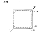
- FIG. 2 is a plan view of the semiconductor device according to the first embodiment of the present invention when the structure of FIG. 1 is viewed from above.
- FIG. 1 shows an end portion of a cross-sectional view taken along a plane perpendicular to the paper surface, including the line segment AA in FIG. That is, the end portion of the semiconductor chip 4 shown on the left side of FIG. 1 corresponds to a corner portion.
- this structure there are regions where the solder thin plate 2 d and the back electrode 6 d are separated by the gap 6 at the four corners of the semiconductor chip 4.
- a boundary 60 between the region where the back electrode 5 d and the solder thin plate 2 d are joined and the gap 6 is schematically shown by a one-dot chain line.
- the bonding boundary 60 has a large radius of curvature near the corner of the semiconductor chip, the stress generated at the interface due to the temperature change is alleviated, and the probability that the solder thin plate is cracked is reduced.
- the semiconductor chip 4 is turned upside down, and the solder thin plate 20d is disposed on the surface of the back electrode 5d.
- an oxide film 3d exists on the surface of the solder thin plate 20d of the Al—Zn alloy when it is exposed to the atmosphere, and the oxide film does not break even if heated to the melting point or higher as it is, and the back metal 5d becomes Al— Even a Zn-based alloy and a wet metal do not join. Therefore, in this state, the solder thin plate 20d is ultrasonically bonded to the back surface metal 5d using an ultrasonic bonder (semiconductor chip bonding step).
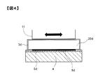
- reference numeral 11 denotes a bonding jig for applying ultrasonic waves
- 8d denotes a locally crushed oxide film 3d by applying ultrasonic waves
- metals are bonded together by ultrasonic bonding.
- This is a partially alloyed region.
- the oxide film 3d existing in this region is pulverized and exists in the vicinity of this region, but does not affect the electrical conduction or the bonding strength.
- the structure in which the semiconductor chip 4 and the solder thin plate 20d are combined is returned to the original upright posture, and this time, the solder thin plate 20d is disposed so as to face the metal plate 1d. To do. At this time, since the semiconductor chip 4 and the solder thin plate 20d are joined, there is no worry of positional displacement. And both are ultrasonically bonded as shown in FIG. 6 (metal plate bonding step).
- reference numeral 12 is a bonding jig for fixing the semiconductor chip 4 and applying ultrasonic waves
- 9d is a region where the oxide film 3d is locally broken by this second ultrasonic application and the metals are alloyed. is there.
- the apparatus used in this step is the same as that used for flip chip bonding by ultrasonic bonding.
- the oxide film 3d existing in this region is pulverized and exists in the vicinity of this region, but does not affect the electrical conduction or the bonding strength.
- the solder thin plate 20 d and the metal plate 1 d are ultrasonically bonded as described above is heated to a temperature higher than the melting point of the Al—Zn alloy, the inside of the solder thin plate 20 d becomes liquid and becomes super In the sonic bonded regions 8d and 9d (see FIG. 6), the alloying reaction proceeds with a part of the metal plate 1d and the back surface metal 5d, and when solidified, solid bonding is established (alloying step). Then, the region other than the region ultrasonically bonded in advance does not progress to the surroundings as shown in FIG. 1 due to the presence of the oxide film 3d.
- a semiconductor chip can be bonded to a metal plate using an Al—Zn alloy without using a special substance or a pressurizing device.
- the solder thin plate 20d is first ultrasonically bonded to the back surface of the semiconductor chip 4.
- the solder thin plate 20d is first ultrasonically bonded to the metal plate 1d as shown in FIG.
- the members may be superposed from the beginning as shown in FIG. 6 and ultrasonically bonded together.
- the gap 6 in FIG. 1 is formed by performing ultrasonic bonding only inside the boundary indicated by a one-dot chain line in FIG. 2 in the first ultrasonic bonding step shown in FIG. be able to.
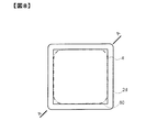
- the size of the solder thin plate 2d is shown to be almost the same as that of the semiconductor chip 4, but the solder thin plate 2d may be larger than the semiconductor chip 4 as shown in FIG.
- the cross-sectional structure perpendicular to the paper surface, including the line segment AA in the figure, has a shape as shown in FIG. 9 due to the presence of the oxide film 3d described above.
- the shape of the solder thin plate 2d is circular as shown in FIG. 10 or a square with rounded corners as shown in FIG. You can also.
- FIG. 12 shows a metal plate 1s serving as a wiring in which a main electrode 5s and a control electrode 5g existing on the surface of the semiconductor chip 4 are attached to the surface of the insulating plate 7 via corresponding thin solder plates 2s and 2g. 1g is connected to 1g.
- a bonding material that is once melted during the assembly process and then solidified, there is a possibility that the solder thin plates 2s and 2g in the drawing are short-circuited when the alloy is melted. Therefore, in general, a measure has been taken in which the distance between the solder thin plates 2s and 2g is sufficiently separated from the solder thickness.
- the width of the passivation film see reference numeral 10 in FIGS.
- the formed solder thin plates 20s and 20g are arranged on the surface electrodes 5s and 5g of the semiconductor chip 4, respectively, and the load and ultrasonic waves are applied by the jig 11 of the ultrasonic bonder as shown in FIG. Is applied to form joint portions 8s and 8g (semiconductor chip joining step).
- the oxide films 3 s and 3 g are locally pulverized, and the metals are alloyed by frictional heat generated by applying the ultrasonic wave.
- the structure is inverted as shown in FIG. 15 and arranged so as to face the metal wirings 1s and 1g formed on the insulating plate 7. As shown in FIG. Then, a load and an ultrasonic wave are applied to form joint portions 9s and 9g (metal plate joining step).
- the ultrasonic bonding regions 8s, 8g, 9s, and 9g proceed with the alloying reaction, and are integrated with the solder thin plates 2s and 2g, respectively, and when solidified, solid bonding is established ( Alloying process). Then, as shown in FIG.
- the oxide film is exclusively alumina.
- a semiconductor chip can be bonded to a metal plate using an Al—Zn alloy without using a special substance or a pressurizing device.
- FIG. 17 shows a mounting cross-sectional structure corresponding to FIG. 12 in a cross section including the line segment BB in FIG. 17 and perpendicular to the paper surface.
- the oxide film 3s is present on the surface of the solder thin plate 2s, the fact that the solder thin plate 2s straddles the runner 50g is not short-circuited as shown in this figure, and as shown in the figure, the runner 50g Even if it is not covered with an insulating film, the main electrode solder thin plate 2s can be provided across the runner 50g as shown by the broken line in FIG. 17 to maximize the electrical performance of the transistor chip. Of course, this structure is established even when the runner 50g is covered with a separate insulating film.
Landscapes
- Engineering & Computer Science (AREA)
- Mechanical Engineering (AREA)
- Die Bonding (AREA)
Abstract
【課題】工業的に簡便な手法によってZn合金系ハンダを利用できるようにするとともに、大きな温度変化を繰り返し経験しても電気的機械的に接合の特性が維持できる構造を実現する。 【解決手段】半導体チップ上4の金属電極5dと金属板1dとをZn-Al系合金製のハンダ板で接合するにあたり、使用時に応力が集中する半導体チップの角部を避けるため、角を丸めた四角形領域のみ、超音波接合法にて前記ハンダ板の表面に存在する金属酸化皮膜3dを破砕して接合させる半導体チップ接合工程と、前記ハンダ板の他方の主面を金属板上に対向させて同じく超音波接合法にて然るべき領域の前記金属酸化皮膜を破砕して接合させる金属板接合工程と、加熱して前記Zn-Al系合金を溶融させ、前記第1の接合領域と前記第2の接合領域とに強固な合金領域を形成する合金化工程とを実施し、これにより側面は酸化皮膜の存在によって応力に強い曲面形状となる。
Description
本発明は、Zn-Al酸化膜を使用した選択的はんだ接合構造を含む半導体装置及びその製造方法に関し、特に、高耐熱パワー半導体チップの電極と配線とを接合した半導体装置及びその製造方法に関する。
従来、縦型半導体チップの電極に外部配線を接続するために、ハンダ合金が使われている。すなわち、金属製の基板の上に板状のハンダを乗せ、その上に、裏面に1つの電極をもつ縦型半導体チップを乗せて加熱し、ハンダを溶かして冷却して固化させ、接合を成立させる。これにより、縦型半導体チップはハンダ層を介して基板上に接合される。
Si半導体素子の場合、Siの物性からその動作の安全性を保障できる上限温度はおよそ150℃とされており、これに従って接続に使われるハンダ合金はこのような上限温度でも溶けず、所定の範囲の温度変化を繰り返し経験しても電気的、機械的特性に問題の生じない材料や厚みやその他諸条件が選択され使われてきた。その結果として従来、融点が前記した温度よりも100℃以上高いものが選択されている。
ところで、SiCなどワイドバンドギャップ半導体で作られた半導体素子は250℃を超える温度でも動作可能であるが、この特性を活かすためには実装に用いるハンダ材の特性もこれに応じたものでなければならない。しかしながら、従来よりも大きな温度差を繰り返し経験しても、長期にわたって信頼性を確保できる材料は限られる。一例としてAu系合金ハンダがあるが高価である。他の例としてZn系合金ハンダがあるが、大気中ではこの合金の表面には金属酸化物による皮膜(以下、「酸化皮膜」という)が形成され、これが接合形成の妨げになる。
例えば、特許文献2においては、このような問題に対する対処法として、Zn-Bi系合金ハンダを接合材として用いるにあたり、酸化皮膜の形成前に保護被覆膜を表面に与えて表面酸化の進行を抑制する方法を開示している。さらにこの保護被覆膜は、ハンダの溶融工程においては速やかに消失し、良好な接合を与える。
また、特許文献3においては、半導体チップと金属基板の間に酸化皮膜に被覆されたZn-Alハンダ板を挟み、この構造に荷重をかけながら加熱することで、溶融したハンダの内圧によって酸化皮膜を破ることによって、溶融ハンダを半導体チップ裏面の金属電極ならびに金属基板と濡れさせて、接合を形成する方法を開示している。
しかしながら、特許文献2の手法においては、酸化防止用の被覆膜として特殊な物質を要し、さらにプリフォームした板ハンダの再整形や搬送時の傷などにより被覆膜によって保護されない部分が発生し性能が劣化する可能性に注意しなければならない。
また、特許文献3の方法では、接合形成時に相応の荷重をかける特殊な装置を必要とする。
本発明は、かかる課題を解決するためになされたもので、Zn系合金ハンダを使いつつ、特殊な被覆膜や荷重印加装置を用いず、工業的に簡便な手法によってZn系合金ハンダを利用できるようにするとともに、これまで接合に対する障害とみなされてきた酸化皮膜の存在を積極的に活用し、大きな温度変化を繰り返し経験しても電気的機械的に接合の特性が維持できる構造を有する半導体装置とその製造方法を提供するものである。
本発明による半導体装置には、金属電極が形成された半導体チップと外部配線である金属板とが、Zn-Al系合金からなるハンダ薄板を介して接合され、前記ハンダ薄板は、角を丸めた四角形をなす第1の接合領域にて前記金属電極と接合するとともに、前記第1の接合領域に対向する主面上の第2の接合領域にて前記金属板と接合し、前記第1の接合領域と前記第2の接合領域の表面が酸化皮膜で被覆されていることを特徴とするものがある。これにより、温度変化によって応力が最も集中する、半導体チップの角部に隣接するハンダ薄板への応力を緩和し、接続信頼性が向上する。
また、上記した発明において、前記ハンダ薄板は、その平面形状が円形もしくは角を丸めた四角形をなすように構成してもよい。これによって、ハンダ薄板の形状を予め上記半導体チップの角部を避けた形状にしておくため、そもそも半導体チップの角部へのハンダ薄板の接触が起こらない。
また、本発明による半導体装置は、半導体チップの一主面に形成された第1の金属電極(たとえば主電極)及び第2の金属電極(たとえば制御電極)と、外部配線である第1の金属板(ここでは主電極用)及び第2の金属板(ここでは制御電極用)とが接合された構成であって、前記第1の電極(主電極)は前記第1の金属板(主電極用配線)と、前記第2の電極(制御電極)は前記第2の金属板(制御電極用配線)と、それぞれZn-Al系合金からなるハンダ薄板を介して接合され、各ハンダ薄板のうち接合に寄与していない側面が酸化皮膜で被覆されていることを特徴とする構成がある。これによって、主電極と制御電極に対して、酸化皮膜によって両電極が短絡する可能性を回避でき、きわめて隣接して接合領域を設けることができるため、主電極の面積に最大限、接合領域を形成することができるとともに、主電極用と制御電極用のハンダ薄板が近接しても短絡することがなくなる。
また、上記の構成においてさらに、一般のトランジスタチップのように第2の金属電極(制御電極)が一部に棒状の領域をもち、第1の金属電極(主電極)がその棒状領域を囲うように配置されている場合に、主電極用の第1のハンダ薄板は第2の金属電極(制御電極)に属する棒状領域の上を跨いで存在し、それでも棒状領域を含めた第2の金属電極(制御電極)と主電極に接続する第1のハンダ薄板との間には酸化皮膜が介在している、構成もある。これによって主電極と制御電極のそれぞれに連絡するハンダ領域の面積が最大化でき、半導体チップの主電流を流れる電流に対して実装構造の電気伝導度が向上する。また、酸化皮膜があることから、たとえ半導体チップ上の制御電極につながるランナーが保護膜なしで存在していても、その上に跨って主電極用のハンダ薄板を形成でき、さらに半導体実装構造の実装抵抗低減に貢献する。
さらに、本発明による金属電極が形成された半導体チップと金属板とを、Zn-Al系合金からなるハンダ薄板を介して接合する半導体装置の製造方法は、前記半導体チップの前記金属電極と前記ハンダ薄板の第1の面とを超音波接合して第1の接合領域を形成する半導体チップ接合工程と、前記金属板と前記ハンダ薄板の前記第1の面に対向する第2の面とを超音波接合して第2の接合領域を形成する金属板接合工程と、少なくとも前記ハンダ薄板を加熱して溶融させて、前記第1の接合領域と前記第2の接合領域とに合金領域を形成する合金化工程と、含むことを特徴とする。これにより、接合したい領域の酸化皮膜を破砕して予め金属同士を接合させておくため、あとは加熱のみによって金属同士が接合する。また、接合させたい領域だけ酸化皮膜を破砕して先に金属同士を接合させておくため、所望の位置に、所望の形状で強固な接合領域を形成できる。
以下、本発明の第1の実施形態による半導体装置について、図1乃至図11を使って説明する。
図1は、本発明の第1の実施形態による半導体装置を示す構造断面図である。図中、1dは金属板で、少なくとも最表面はAl、Ag、Au、Cu、Niなどが可能である。すなわち、1dは図のように分厚い金属板でもよいし、図示しない別の金属板状上に形成された薄膜でもよい。2dはハンダ薄板でAl-Zn系の合金からなる。3dはハンダを構成する金属が自然酸化して出来た酸化皮膜で、ハンダ薄板2dが大気と触れる部分にすべて存在する。4は半導体チップ、5dは半導体チップ4の裏面電極である。裏面電極5dはハンダ薄板2dを介して金属板1dに電気的かつ機械的に接続されている。また図中、半導体チップ4の角部においては、ハンダ薄板2dとの間には空隙6が存在する。
図2は、本発明の第1の実施形態による半導体装置であって、図1の構造を上から見た平面図である。なお、図2の線分A-Aを含み、紙面に垂直な面で切った断面図の端部が図1である。すなわち、図1の左側に示した半導体チップ4の端部は角部に相当する。本構造において、半導体チップ4の四隅にはハンダ薄板2dと裏面電極6dとが空隙6によって隔たった領域が存在する。図2では、裏面電極5dとハンダ薄板2dが接合している領域と空隙6との境界60を一点鎖線で模式的に示した。このように接合境界60が半導体チップの角部付近にて接合境界が大きな曲率半径をもっていると、温度変化によってこの界面に生じる応力は緩和され、ハンダ薄板にクラックが入る確率を低める。
次に、このような構造を成立させるための製造方法を、図3乃至図7を使って説明する。まず、図3のように半導体チップ4の裏面を上にして倒立させ、上になった裏面電極5dの表面にハンダ薄板20dを配置する。ところで、Al-Zn系合金のこのハンダ薄板20dの表面には、大気に触れた時点で酸化皮膜3dが存在し、このまま融点以上に加熱しても酸化皮膜が破れず、裏面金属5dがAl-Zn系合金と濡れる金属であっても両者は接合しない。そこで、この状態で超音波ボンダーを使ってハンダ薄板20dを裏面金属5dに超音波接合しておく(半導体チップ接合工程)。図4はこのプロセスを示したもので、図中、符号11は超音波を印加するボンディング治具、8dは超音波印加によって局所的に酸化皮膜3dが破砕され、金属同士が超音波接合によって一部合金化した領域である。なお、この領域にあった酸化皮膜3dは粉砕されてこの領域付近に存在するが、電気伝導や接合強度には影響しない。
次に、図5に示すように、この半導体チップ4とハンダ薄板20dが結合した構造体を、もとの正立の姿勢に戻し、今度はハンダ薄板20dが金属板1dと対面するように配置する。この時点で半導体チップ4とハンダ薄板20dは結合しているので位置ズレの心配はない。そして、図6のように両者を超音波接合する(金属板接合工程)。図中、符号12は半導体チップ4を固定して超音波を印加するボンディング治具、9dはこの第2回目の超音波印加によって局所的に酸化皮膜3dが破れ、金属同士が合金化した領域である。この工程で使用する装置は、超音波接合によるフリップチップボンディングする際と同様のものである。なお、この領域にあった酸化皮膜3dは粉砕されてこの領域付近に存在するが、電気伝導や接合強度には影響しない。
次に、上記のとおり半導体チップ4とハンダ薄板20dと金属板1dとを超音波接合した構造体をAl-Zn系合金の融点以上に加熱してやると、ハンダ薄板20dの内部は液状になり、超音波接合した領域8d、9d(図6参照)は、金属板1dや裏面金属5dの一部と合金化反応が進み、固化した際には強固な接合が成立している(合金化工程)。そして、あらかじめ超音波接合した領域以外は酸化皮膜3dの存在により図1に示すように、周囲に進展することはない。このように、本発明によれば、特別な物質や加圧装置を用いずともAl-Zn系合金を使って半導体チップを金属板に接合することができる。
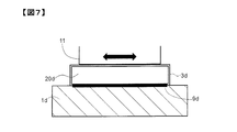
なお、上記のプロセスではハンダ薄板20dをまず半導体チップ4の裏面に超音波接合したが、図7に示すようにハンダ薄板20dを先に金属板1dに超音波接合してから、図6のプロセスを実施しても当然構わないし、最初から図6のように部材を重ね合わせて、一括して超音波接合しても構わない。
また、図1中の空隙6は、図4で示した第1回目の超音波接合工程において、図2に1点鎖線で示した境界の内側だけ超音波接合するようにしておくことで形成することができる。
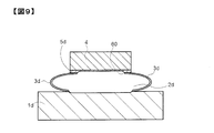
また、図2ではハンダ薄板2dのサイズを半導体チップ4とほぼ同じに示したが、例えば図8のようにハンダ薄板2dが半導体チップ4より大きくても構わない。その場合、図中の線分A-Aを含んで紙面に垂直な断面構造は、前述した酸化皮膜3dの存在のため、図9のような形状になる。
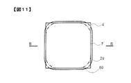
また、空隙6を形成したい領域に、そもそもハンダ薄板2dが近接しないよう、図10に示すようにハンダ薄板2dの形状を円形、もしくは図11に示すように角部を丸めた四角形にしておくこともできる。
次に、本発明の第2の実施形態による半導体装置ついて、図12乃至図16を使って説明する。
図12は、半導体チップ4の表面に存在する主電極5sと制御電極5gが、それぞれに対応するハンダ薄板2s、2gを介して、絶縁板7の表面に張り付けられ配線の役割を果たす金属板1s、1gに接続している構造である。このような構造を、組立工程中に一度溶融してから固化する接合材を使う場合、合金が溶融した時点で図中のハンダ薄板2sと2gとが短絡する可能性がある。そのため一般には、ハンダ薄板2sと2gの距離を、ハンダ厚みより十分離しておく方策が取られていた。しかし、実際の半導体チップ4の表面で主電極5sと制御電極5gを隔てるパッシベーション膜(図13乃至図16の符号10参照)の幅はせいぜい数十μmであるのに対し。ハンダ厚みは50μm以上あるので、この場合、ハンダ薄板2sと2gの距離は最低でも300μm以上は隔てることになる。しかし、そのような施策は半導体チップの電気特性を損なう方向に働く。
一方、Al-Zn系合金からなるハンダの場合、図12に示すようにそれぞれのハンダ薄板の表面には強固な酸化皮膜3s、3gが形成され、ハンダが溶融しても容易には破れない。この性質を利用し、本発明では半導体チップ4上の金属と配線金属とは接続しつつ、上記の短絡は起きにくいため、両者を近接させて配置することが可能で、半導体チップの電気特性を十分に生かした実装構造を実現できる。
次に、図12に示す半導体装置の製造方法の一例について、図13乃至図16を使って説明する。まず図13のように、半導体チップ4の表面電極5s、5gの上に、成形したハンダ薄板20s、20gをそれぞれ配置し、図14のように超音波ボンダーの治具11にて荷重と超音波を印加し、接合箇所8s、8gを形成する(半導体チップ接合工程)。この超音波印加によって局所的に酸化皮膜3s、3gは粉砕され、金属同士が超音波印加による摩擦熱によって合金化する。
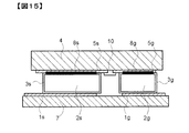
次に図15のように上記の構造体を倒立させて絶縁板7上に形成された金属配線1s、1gと対向するように配置し、図16に示すように超音波ボンダーの治具11にて荷重と超音波を印加し、接合箇所9s、9gを形成する(金属板接合工程)。
次に、上記のとおり半導体チップ4と絶縁板7とをハンダ薄板2s、2gを介して超音波接合した構造体をAl-Zn系合金の融点以上に加熱してやると、ハンダ薄板の内部は液状になり、超音波接合した領域8s、8g、9s、9g(図16参照)は合金化反応が進み、それぞれハンダ薄板2s、2gと一体化し、固化した際には強固な接合が成立している(合金化工程)。そして、図12に示すように酸化皮膜3s、3gの存在により超音波接合した領域以外は流れ出ることはなく、ハンダ薄板の端部は樽型の断面形状になり、3sと3gが近接しても、短絡することはない。ちなみに、共晶系のAl-Znハンダの場合、酸化皮膜はもっぱらアルミナである。このように、本発明によれば、特別な物質や加圧装置を用いずともAl-Zn系合金を使って半導体チップを金属板に接合することができる。
また、一般の電力用トランジスタチップの表面電極パターンは図17のようになっていて、制御信号を素早くチップ内に行き渡らせるため、制御電極5gに接続された細長いランナー50gが、主電極5sの中央に延在するものがある。また、図17中の線分B-Bを含み紙面に垂直な断面で、図12に対応した実装断面構造が図18である。ハンダ薄板2sの表面には酸化皮膜3sが存在するので、この図に示すようにハンダ薄板2sがランナー50gを跨いでいても短絡することはないことを利用し、仮に図中のようにランナー50gが絶縁膜で被覆されていなくても、主電極用ハンダ薄板2sを図17中の破線のように、ランナー50gを跨いで存在させ、トランジスタチップの電気的性能を最大限に引き出すことができる。もちろん、ランナー50gが別途の絶縁膜によって覆われていてもこの構造は成立する。
以上、本発明による半導体装置及びその製造方法の実施例及びこれに基づく変形例を説明したが、本発明は必ずしもこれらに限定されるものではなく、当業者であれば、本発明の主旨又は特許請求の範囲に合致すれば、他の構成でも本発明の権利範囲に属する。
1d、1s、1g 金属板
2d、2s、2g、20d、20s、20g ハンダ薄板
3d、3s、3g 酸化皮膜
4 半導体チップ
5d (半導体チップの)裏面金属
5s (半導体チップの)主電極
5g (半導体チップの)制御電極
50g ランナー
6 空隙
60 境界
7 絶縁板
8d、8s、8g 半導体チップとハンダ薄板との間の超音波接合箇所
9d、9s、9g 金属板あるいは絶縁板とハンダ薄板との間の超音波接合箇所
11、12 ボンディング治具
2d、2s、2g、20d、20s、20g ハンダ薄板
3d、3s、3g 酸化皮膜
4 半導体チップ
5d (半導体チップの)裏面金属
5s (半導体チップの)主電極
5g (半導体チップの)制御電極
50g ランナー
6 空隙
60 境界
7 絶縁板
8d、8s、8g 半導体チップとハンダ薄板との間の超音波接合箇所
9d、9s、9g 金属板あるいは絶縁板とハンダ薄板との間の超音波接合箇所
11、12 ボンディング治具
Claims (5)
- 金属電極が形成された半導体チップと金属板とが、Zn-Al系合金からなるハンダ薄板を介して接合された半導体装置であって、
前記ハンダ薄板は、角を丸めた四角形をなす第1の接合領域にて前記金属電極と接合するとともに、前記第1の接合領域に対向する主面上の第2の接合領域にて前記金属板と接合し、前記第1の接合領域と前記第2の接合領域の表面が酸化皮膜で被覆されていることを特徴とする半導体装置。 - 前記ハンダ薄板は、その平面形状が円形もしくは角を丸めた四角形をなしていることを特徴とする請求項1記載の半導体装置。
- 半導体チップの一主面に形成された第1の金属電極及び第2の金属電極と、第1の金属板及び第2の金属板とが接合された半導体装置であって、
前記第1の電極は前記第1の金属板とZn-Al系合金からなる第1のハンダ薄板を介して接合され、前記第1のハンダ薄板のうち前記接合に寄与していない側面が酸化皮膜で被覆されており、
前記第2の電極は前記第2の金属板とZn-Al系合金からなる第2のハンダ薄板を介して接合され、前記第2のハンダ薄板のうち前記接合に寄与していない側面が酸化皮膜で被覆されていることを特徴とする半導体装置。 - 前記第2の金属電極は一部に棒状の領域を有し、前記第1の金属電極は前記棒状領域を囲うように配置されていて、前記第1のハンダ薄板は前記第2の金属電極に属する前記棒状領域を跨いで存在し、前記棒状領域を含め前記第2の金属電極と前記第1のハンダ薄板との間には酸化皮膜が介在している、ことを特徴とする請求項3記載の半導体装置。
- 金属電極が形成された半導体チップと金属板とを、Zn-Al系合金からなるハンダ薄板を介して接合する半導体装置の製造方法であって、
前記半導体チップの前記金属電極と前記ハンダ薄板の第1の面とを超音波接合して第1の接合領域を形成する半導体チップ接合工程と、
前記金属板と前記ハンダ薄板の前記第1の面に対向する第2の面とを超音波接合して第2の接合領域を形成する金属板接合工程と、
少なくとも前記ハンダ薄板を加熱して溶融させて、前記第1の接合領域と前記第2の接合領域とに合金領域を形成する合金化工程とを、含むことを特徴とする半導体装置の製造方法。
Applications Claiming Priority (2)
| Application Number | Priority Date | Filing Date | Title |
|---|---|---|---|
| JP2016-206963 | 2016-10-21 | ||
| JP2016206963A JP6732189B2 (ja) | 2016-10-21 | 2016-10-21 | 半導体装置及びその製造方法 |
Publications (1)
| Publication Number | Publication Date |
|---|---|
| WO2018074146A1 true WO2018074146A1 (ja) | 2018-04-26 |
Family
ID=62018556
Family Applications (1)
| Application Number | Title | Priority Date | Filing Date |
|---|---|---|---|
| PCT/JP2017/034445 Ceased WO2018074146A1 (ja) | 2016-10-21 | 2017-09-25 | 半導体装置及びその製造方法 |
Country Status (2)
| Country | Link |
|---|---|
| JP (1) | JP6732189B2 (ja) |
| WO (1) | WO2018074146A1 (ja) |
Citations (2)
| Publication number | Priority date | Publication date | Assignee | Title |
|---|---|---|---|---|
| JP2009113050A (ja) * | 2007-11-02 | 2009-05-28 | Ibaraki Univ | Zn−Al共析系合金接合材、Zn−Al共析系合金接合材の製造方法、Zn−Al共析系合金接合材を用いた接合方法及びZn−Al共析系合金接合材を用いた半導体装置 |
| JP2016225552A (ja) * | 2015-06-03 | 2016-12-28 | 国立大学法人茨城大学 | 高耐熱ハンダ接合半導体装置及びその製造方法 |
-
2016
- 2016-10-21 JP JP2016206963A patent/JP6732189B2/ja active Active
-
2017
- 2017-09-25 WO PCT/JP2017/034445 patent/WO2018074146A1/ja not_active Ceased
Patent Citations (2)
| Publication number | Priority date | Publication date | Assignee | Title |
|---|---|---|---|---|
| JP2009113050A (ja) * | 2007-11-02 | 2009-05-28 | Ibaraki Univ | Zn−Al共析系合金接合材、Zn−Al共析系合金接合材の製造方法、Zn−Al共析系合金接合材を用いた接合方法及びZn−Al共析系合金接合材を用いた半導体装置 |
| JP2016225552A (ja) * | 2015-06-03 | 2016-12-28 | 国立大学法人茨城大学 | 高耐熱ハンダ接合半導体装置及びその製造方法 |
Also Published As
| Publication number | Publication date |
|---|---|
| JP6732189B2 (ja) | 2020-07-29 |
| JP2018067679A (ja) | 2018-04-26 |
Similar Documents
| Publication | Publication Date | Title |
|---|---|---|
| JP4908750B2 (ja) | 半導体装置 | |
| JP6433590B2 (ja) | 電力用半導体装置の製造方法および電力用半導体装置 | |
| JP6033011B2 (ja) | 電力用半導体装置および電力用半導体装置の製造方法 | |
| JP5903637B2 (ja) | 導電路の製造方法及び半導体装置の製造方法 | |
| US20080122050A1 (en) | Semiconductor Device And Production Method For Semiconductor Device | |
| JP2002289768A (ja) | 半導体装置およびその製法 | |
| JP6479036B2 (ja) | 半導体装置及びその製造方法 | |
| JP2015128194A (ja) | 半導体装置 | |
| JP2009016583A (ja) | 半導体装置およびその製造方法 | |
| CN111448655B (zh) | 在半导体器件和热交换器间产生热界面键合的装置和方法 | |
| WO2012053129A1 (ja) | 半導体装置及びその製造方法 | |
| JP6091443B2 (ja) | 半導体モジュール | |
| JP6008750B2 (ja) | 半導体装置 | |
| JPH0823002A (ja) | 半導体装置及びその製造方法 | |
| JP5799565B2 (ja) | 半導体装置及びその製造方法 | |
| JP6732189B2 (ja) | 半導体装置及びその製造方法 | |
| JP7432075B2 (ja) | パワー半導体モジュール | |
| JP6304085B2 (ja) | 半導体装置及び半導体装置の製造方法 | |
| JP6427838B2 (ja) | 半導体装置 | |
| JP2018085421A (ja) | 半導体装置 | |
| JP2012094643A (ja) | 半導体装置及びその製造方法 | |
| JP2003297874A (ja) | 電子部品の接続構造及び接続方法 | |
| JP6931869B2 (ja) | 半導体装置 | |
| WO2021149637A1 (ja) | 電子装置および電子装置の製造方法 | |
| JPH03268340A (ja) | 半導体装置 |
Legal Events
| Date | Code | Title | Description |
|---|---|---|---|
| 121 | Ep: the epo has been informed by wipo that ep was designated in this application |
Ref document number: 17862344 Country of ref document: EP Kind code of ref document: A1 |
|
| NENP | Non-entry into the national phase |
Ref country code: DE |
|
| 122 | Ep: pct application non-entry in european phase |
Ref document number: 17862344 Country of ref document: EP Kind code of ref document: A1 |