WO2018074063A1 - シリコンウェーハの製造方法 - Google Patents
シリコンウェーハの製造方法 Download PDFInfo
- Publication number
- WO2018074063A1 WO2018074063A1 PCT/JP2017/030670 JP2017030670W WO2018074063A1 WO 2018074063 A1 WO2018074063 A1 WO 2018074063A1 JP 2017030670 W JP2017030670 W JP 2017030670W WO 2018074063 A1 WO2018074063 A1 WO 2018074063A1
- Authority
- WO
- WIPO (PCT)
- Prior art keywords
- silicon wafer
- acid
- etching
- spin
- etching solution
- Prior art date
- Legal status (The legal status is an assumption and is not a legal conclusion. Google has not performed a legal analysis and makes no representation as to the accuracy of the status listed.)
- Ceased
Links
Images





Classifications
-
- B—PERFORMING OPERATIONS; TRANSPORTING
- B23—MACHINE TOOLS; METAL-WORKING NOT OTHERWISE PROVIDED FOR
- B23K—SOLDERING OR UNSOLDERING; WELDING; CLADDING OR PLATING BY SOLDERING OR WELDING; CUTTING BY APPLYING HEAT LOCALLY, e.g. FLAME CUTTING; WORKING BY LASER BEAM
- B23K26/00—Working by laser beam, e.g. welding, cutting or boring
-
- H—ELECTRICITY
- H10—SEMICONDUCTOR DEVICES; ELECTRIC SOLID-STATE DEVICES NOT OTHERWISE PROVIDED FOR
- H10P—GENERIC PROCESSES OR APPARATUS FOR THE MANUFACTURE OR TREATMENT OF DEVICES COVERED BY CLASS H10
- H10P50/00—Etching of wafers, substrates or parts of devices
-
- H—ELECTRICITY
- H10—SEMICONDUCTOR DEVICES; ELECTRIC SOLID-STATE DEVICES NOT OTHERWISE PROVIDED FOR
- H10P—GENERIC PROCESSES OR APPARATUS FOR THE MANUFACTURE OR TREATMENT OF DEVICES COVERED BY CLASS H10
- H10P52/00—Grinding, lapping or polishing of wafers, substrates or parts of devices
Definitions
- the present invention relates to a method for manufacturing a silicon wafer.
- a wafer sliced thinly from a single crystal ingot is generally flattened through chamfering and grinding, and a unique number of the wafer is printed by laser mark processing.
- various scratches and distortions due to processing are introduced on the front and back surfaces of the wafer, and if these become obvious in the subsequent process, it may become a serious quality problem.
- etching is usually performed after laser mark processing to remove scratches and processing distortion.
- an etching method there are known a batch method in which front and back surfaces of a plurality of wafers are simultaneously processed and a spin etching method in which the front and back surfaces of a wafer are processed in order in a single wafer (see Patent Document 1). Further, there are two methods depending on the purpose: treatment with an acid etching solution and treatment with an alkaline etching solution.
- the present invention has been made in view of the above-described problems, and an object of the present invention is to provide a method for manufacturing a silicon wafer that can reduce etching unevenness in the vicinity of laser mark dots.
- the present invention is configured to rotate the silicon wafer while supplying the acid etching solution to the front or back surface of the silicon wafer through a supply nozzle, thereby reducing the supply range of the acid etching solution.
- a silicon wafer manufacturing method including a spin etching process in which acid etching is performed by enlarging the entire surface or back surface of the silicon wafer, wherein in the spin etching process, the spin rotation speed of the silicon wafer is 1000 rpm or less, and the viscosity is Provided is a method for producing a silicon wafer, characterized by using the acid etching solution of 6.0 mPa ⁇ s or less.
- the acid etching solution a mixed solution containing hydrofluoric acid, nitric acid, and sulfuric acid, or a mixed solution obtained by adding acetic acid to the mixed solution can be used.
- the above mixed solution can be used.
- the acid etching solution a mixed solution containing 1 to 10% by mass of hydrofluoric acid, 25 to 50% by mass of nitric acid, 0 to 15% by mass of acetic acid, and 5 to 25% by mass of sulfuric acid is used. it can.
- the acid etching solution having a viscosity of 6.0 mPa ⁇ s or less a mixed solution in which an acid is mixed in the above ratio can be used.
- the spin etching process can be performed after a laser marking process in which a mark is engraved by a laser on the front surface or the back surface of the silicon wafer.
- the spin etching process according to the present invention is effective in reducing the streaky etching unevenness in the vicinity of the laser mark dots engraved in the laser marking process.
- the silicon wafer manufacturing method of the present invention can reduce etching unevenness, and in particular, can reduce etching unevenness in the vicinity of laser mark dots.
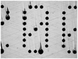
- FIG. 3 is a photograph observing streaky etching unevenness of the wafer after etching in Example 1.
- FIG. It is the photograph which observed the stripe-shaped etching nonuniformity of the wafer after the etching of the comparative example 2.
- FIG. 5 is a graph showing the depth (height difference) of etching unevenness of wafers after etching in Examples 1 to 3 and Comparative Examples 1 and 2;
- FIG. 6 is a photograph observing streaky etching unevenness of a wafer after etching in Example 5.
- FIG. It is the photograph which observed the stripe-shaped etching nonuniformity of the wafer after the etching of the comparative example 5.
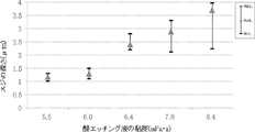
- FIG. 7 is a graph showing the depth (height difference) of etching unevenness of wafers after etching in Examples 4 and 5 and Comparative Examples 3 to 5.
- 6 is a graph showing a double-sided polishing allowance required for wafers after etching in Examples 4 and 5 and Comparative Examples 3 to 5. It is a photograph which shows an example of the stripe-shaped etching nonuniformity which generate
- the present inventor has discovered that the generation of streaky etching unevenness near the laser mark dot is caused by the cavity flow when the acid etching solution as the fluid flows on the laser mark dot. This is considered that when the acid etching solution flows over the laser mark dots, a wake behind the cavity occurs along the direction in which the acid etching solution flows from the laser mark dots, and etching unevenness occurs there.
- the present inventor has found that when the spin rotation speed is large, the average flow rate of the etching solution increases, and the etching unevenness generated in the laser mark dot is emphasized.
- the fluid motion can be considered qualitative behavior by the Reynolds number derived from the Navier-Stokes equation
- the present inventors have increased the Reynolds number of the acid etching solution, that is, by reducing the liquid viscosity, the downstream of the cavity. It was confirmed that the generation of etching unevenness due to the above was alleviated, and conversely, when the Reynolds number of the acid etching solution was reduced, that is, the viscosity of the solution was increased, etching unevenness was easily generated.
- the present inventors diligently studied a suitable range of the spin rotation speed and the viscosity of the acid etching solution.
- the spin rotation speed was set to 1000 rpm or less, and the viscosity of the acid etching solution was set to 6.0 mPa ⁇ s. It has been discovered that the following conditions are the conditions that can suppress the occurrence of streaky etching unevenness near the laser mark dots.
- the silicon wafer manufacturing method of the present invention rotates the silicon wafer while supplying the acid etching solution to the front or back surface of the silicon wafer through the supply nozzle, thereby reducing the supply range of the acid etching solution to the front or back surface of the silicon wafer. It includes a spin etching process in which acid etching is performed over the entire surface. Such a spin etching process is performed, for example, after a laser marking process in which a mark is imprinted on the front or back surface of a silicon wafer by a laser.
- processes such as a slicing process in which a silicon single crystal ingot is sliced thinly to produce a silicon wafer, a chamfering process of a silicon wafer, a grinding process, and a polishing process may be included.
- an acid etching solution having a silicon wafer with a spin rotation speed of 1000 rpm or less and a viscosity of 6.0 mPa ⁇ s or less is used.
- Such a spin etching process will be described more specifically with reference to FIG.
- an etching apparatus 1 as shown in FIG. 1 can be used.
- a silicon wafer W to be etched is placed horizontally at the center of the vacuum suction stage 2 with the front or back surface facing up, and is held by vacuum suction on the vacuum suction stage 2 connected to the vacuum source 9. .
- the vacuum suction stage 2 is rotated in the ⁇ direction of FIG. 1 with the center of the vacuum suction stage 2 as a rotation axis by a rotation unit including a ⁇ -axis motor and a ⁇ spindle (not shown) below the stage.
- the spin rotation speed of the silicon wafer W is set to 1000 rpm or less as described above. By setting the spin rotation speed to 1000 rpm or less, the average flow rate of the acid etching solution 8 is suppressed, and the generation of etching unevenness due to the cavity wake is alleviated.
- the spin rotation speed is 1000 rpm or less and 300 rpm or more. If the acid etching solution 8 is supplied at a spin rotation speed of 300 rpm or more, the acid etching solution 8 surely diffuses over the entire surface of the wafer, so that the in-plane distribution of the wafer etching allowance becomes uniform.
- the acid etching solution 8 having a viscosity of 6.0 mPa ⁇ s or less is supplied from the liquid supply source 6 to the supply nozzle 3 above the vacuum suction stage 2 and is held and rotated on the vacuum suction stage 2.
- An acid etching solution 8 is supplied onto the silicon wafer W. If the viscosity of the acid etching solution 8 exceeds 6.0 mPa ⁇ s, the level difference of the etching unevenness generated in the laser mark dots becomes extremely large, and the polishing allowance in the subsequent double-side polishing step must be increased more than necessary.
- the viscosity of the acid etching solution 8 is 6.0 mPa ⁇ s or less and preferably 5.0 mPa ⁇ s or more.
- the viscosity of the acid etching solution 8 is 5.0 mPa ⁇ s or more, the reaction efficiency between the acid etching solution 8 and the silicon wafer 1 is further improved, and a high etching rate can be obtained.
- the acid etching solution 8 having a viscosity of 6.0 mPa ⁇ s or less is not particularly limited, but in addition to a mixed solution containing hydrofluoric acid, nitric acid, and sulfuric acid, or hydrofluoric acid, nitric acid, and sulfuric acid, A mixed solution to which acetic acid has also been added can be used. Further, although not particularly limited, such a mixed solution contains 1 to 10% by mass of hydrofluoric acid, 25 to 50% by mass of nitric acid, 0 to 15% by mass of acetic acid, and 5 to 25% by mass of sulfuric acid. If included in the range, the viscosity is 6.0 mPa ⁇ s or less. In this case, the balance in which the mass% of the acid is less than 100% in total is water.
- the supply nozzle 3 While the acid etching solution 8 is being supplied, the supply nozzle 3 generally reciprocates linearly in the radial direction of the silicon wafer W through the center of the silicon wafer W as indicated by an arrow 4 in FIG. Is.
- the acid etching solution 8 supplied onto the silicon wafer W moves on the silicon wafer W toward the outer periphery by the rotation of the silicon wafer W, and is discharged as droplets 5 from the outer periphery of the silicon wafer W.
- the supply of the acid etching solution 8 from the supply source 6 is stopped, the water is supplied from the water supply source 7 to the supply nozzle 3, and is held and rotated on the vacuum suction stage 2.
- Water is supplied onto the silicon wafer W.
- the water supplied onto the silicon wafer W moves on the silicon wafer W in the outer peripheral direction by the rotation of the silicon wafer W, and the acid etching solution 8 remaining on the silicon wafer W is replaced with water while the silicon wafer W is replaced.
- the liquid is discharged as droplets from the outer peripheral portion.
- Example 1 First, a plurality of silicon wafers having laser mark dots on the surface were prepared through a laser marking process. Next, with respect to each of the prepared silicon wafers, the spin etching process according to the present invention was performed in a single wafer type using the etching apparatus 1 as shown in FIG.
- the spin rotation speed of the silicon wafer was set to 300 rpm, and the viscosity of the acid etching solution was set to 6.0 mPa ⁇ s.
- Example 2 The silicon wafer was spin-etched in a single wafer manner in the same manner as in Example 1 except that the spin rotation number of the silicon wafer was 800 rpm and the spin etching step in the present invention was carried out in a single wafer manner. At this time, the viscosity of the acid etching solution was 6.0 mPa ⁇ s as in Example 1.
- Example 3 The silicon wafer was spin-etched in a single-wafer manner as in Example 1 except that the spin rotation speed of the silicon wafer was 1000 rpm and the spin-etching step in the present invention was carried out in a single-wafer manner. At this time, the viscosity of the acid etching solution was 6.0 mPa ⁇ s as in Example 1.
- Example 1 The silicon wafer was spin-etched in a single-wafer manner as in Example 1 except that the spin rotation speed of the silicon wafer was 1200 rpm and the spin-etching step was carried out in a single-wafer manner. At this time, the viscosity of the acid etching solution was 6.0 mPa ⁇ s as in Example 1.
- Example 2 The silicon wafer was spin-etched in a single-wafer manner as in Example 1 except that the spin rotation speed of the silicon wafer was 2000 rpm and the spin-etching step was carried out in a single-wafer manner. At this time, the viscosity of the acid etching solution was 6.0 mPa ⁇ s as in Example 1.
- Example 1 and Comparative Example 2 streaky etching unevenness near the laser mark dots on the etched wafer was observed with a laser microscope.
- the observation photographs of Example 1 and Comparative Example 2 are shown in FIGS. 2 and 3, respectively.
- FIGS. 2 and 3 The observation photographs of Example 1 and Comparative Example 2 are shown in FIGS. 2 and 3, respectively.
- FIGS. 2 and 3 The observation photographs of Example 1 and Comparative Example 2 are shown in FIGS. 2 and 3, respectively.
- FIGS. 2 and 3 As can be seen from the above, in Example 1 (FIG. 2) in which the spin speed was 1000 rpm or less, streaky etching unevenness was generated compared to Comparative Example 2 (FIG. 3) in which the spin speed was greater than 1000 rpm. It was relaxed.
- FIG. 4 shows the depth (height difference) of etching unevenness in the vicinity of the laser mark dots on the wafers after etching in Examples 1 to 3 and Comparative Examples 1 and 2.
- the height difference was measured by cross section measurement with a laser microscope.
- the spin speed exceeded 1000 rpm, the streak depth increased rapidly. That is, in Comparative Examples 1 and 2, the polishing allowance in the double-side polishing step had to be increased more than in Examples 1 to 3.
- Example 4 The spin etching process was performed under the same conditions as in Example 1 except that the spin rotation number of the silicon wafer was 300 rpm, the viscosity of the acid etching solution was 5.5 mPa ⁇ s, and the other conditions were the same.
- Example 5 A silicon wafer was spin-etched in the same manner as in Example 4 except that the viscosity of the acid etching solution was 6.0 mPa ⁇ s. At this time, the spin rotation number of the silicon wafer was 300 rpm as in Example 4. Thus, Example 5 was made the same conditions as Example 1.
- Example 3 A silicon wafer was spin-etched in the same manner as in Example 4 except that the viscosity of the acid etching solution was 6.4 mPa ⁇ s. At this time, the spin rotation number of the silicon wafer was 300 rpm as in Example 4.
- Example 4 A silicon wafer was spin-etched in the same manner as in Example 4 except that the viscosity of the acid etching solution was 7.0 mPa ⁇ s. At this time, the spin rotation number of the silicon wafer was 300 rpm as in Example 4.
- Example 5 A silicon wafer was spin-etched in the same manner as in Example 4 except that the viscosity of the acid etching solution was 8.4 mPa ⁇ s. At this time, the spin rotation number of the silicon wafer was 300 rpm as in Example 4.
- Example 5 streaky etching unevenness in the vicinity of laser mark dots on the etched wafer was observed with a laser microscope.
- An observation photograph of Example 5 is shown in FIG.
- An observation photograph of Comparative Example 5 is shown in FIG. Comparing FIG. 5 (Example 5) and FIG. 6 (Comparative Example 5), in Example 5 in which the viscosity of the acid etching solution was 6.0 mPa ⁇ s or less, a comparative example in which the viscosity was greater than 6.0 mPa ⁇ s. It can be seen that the occurrence of streaky etching unevenness was alleviated as compared with FIG.
- FIG. 7 shows the depth (height difference) of etching unevenness in the vicinity of the laser mark dots on the wafers after etching in Examples 4 and 5 and Comparative Examples 3 to 5.
- the height difference was measured by cross section measurement with a laser microscope. As can be seen from FIG. 7, when the viscosity exceeded 6.0 mPa ⁇ s, the streak depth increased rapidly.
- FIG. 8 shows a double-sided polishing allowance in a post-process required for the wafers after etching in Examples 4 and 5 and Comparative Examples 3 to 5.
- the viscosity exceeds 6.0 mPa ⁇ s
- the difference in height of the etching unevenness is large, so that the machining allowance required for double-side polishing has increased.
- the present invention is not limited to the above embodiment.
- the above-described embodiment is an exemplification, and the present invention has any configuration that has substantially the same configuration as the technical idea described in the claims of the present invention and that exhibits the same effects. Are included in the technical scope.
Landscapes
- Engineering & Computer Science (AREA)
- Physics & Mathematics (AREA)
- Optics & Photonics (AREA)
- Plasma & Fusion (AREA)
- Mechanical Engineering (AREA)
- Weting (AREA)
- Mechanical Treatment Of Semiconductor (AREA)
- Laser Beam Processing (AREA)
- Cleaning Or Drying Semiconductors (AREA)
Abstract
本発明は、シリコンウェーハの表面又は裏面に供給ノズルを通して酸エッチング液を供給しながら、シリコンウェーハを回転させることで、酸エッチング液の供給範囲をシリコンウェーハの表面又は裏面の全面に拡大して酸エッチングを行うスピンエッチング工程を含むシリコンウェーハの製造方法であって、スピンエッチング工程において、シリコンウェーハのスピン回転数を1000rpm以下とし、かつ、粘度が6.0mPa・s以下の酸エッチング液を用いることを特徴とするシリコンウェーハの製造方法である。これにより、レーザーマークドット付近のエッチングムラを低減することが可能なシリコンウェーハの製造方法が提供される。
Description
本発明は、シリコンウェーハの製造方法に関する。
シリコンウェーハの製造工程において、単結晶インゴットの状態から薄くスライスされたウェーハは、面取り加工と研削加工を経て平坦化を行い、レーザーマーク加工でウェーハの固有番号を印字するのが一般的である。この際、ウェーハ表裏面には加工に起因する大小様々なキズや加工歪みが導入され、これらが後工程で顕在化すると重大な品質上の問題になり得る。
そこで、通常はレーザーマーク加工後にエッチングを行い、キズや加工歪を除去する。エッチング方法としては複数のウェーハの表裏面を同時に処理するバッチ方式や枚葉でウェーハの表面と裏面を順に処理するスピンエッチング方式が知られている(特許文献1参照)。また目的に応じて酸エッチング液で処理する場合とアルカリエッチング液で処理する場合の2通りの手段がある。
ところが、レーザーマーク加工後に、スピンエッチング方式による酸エッチングを行った場合、エッチング液の流れに沿ってレーザーマークドットからウェーハの外周部に向けて、図9のレーザー顕微鏡写真に示すようなスジ状のエッチングムラが生じてしまう。このスジ状のエッチングムラは、高低差が数μmあるため、ウェーハの平坦度を出すためには、後工程の両面研磨(DSP)における取り代を必要以上に増やさなければならないという問題が生じる。
本発明は前述のような問題に鑑みてなされたもので、レーザーマークドット付近のエッチングムラを低減することが可能なシリコンウェーハの製造方法を提供することを目的とする。
上記目的を達成するために、本発明は、シリコンウェーハの表面又は裏面に供給ノズルを通して酸エッチング液を供給しながら、前記シリコンウェーハを回転させることで、前記酸エッチング液の供給範囲を前記シリコンウェーハの表面又は裏面の全面に拡大して酸エッチングを行うスピンエッチング工程を含むシリコンウェーハの製造方法であって、前記スピンエッチング工程において、前記シリコンウェーハのスピン回転数を1000rpm以下とし、かつ、粘度が6.0mPa・s以下の前記酸エッチング液を用いることを特徴とするシリコンウェーハの製造方法を提供する。
本発明のように、スピン回転数を1000rpm以下と小さく設定し、かつ、粘度が6.0mPa・s以下と小さい酸エッチング液を用いることで、レーザーマークドット付近に生じるスジ状のエッチングムラを低減することができる。その結果、後工程の両面研磨工程等における取り代を最小限に抑えることができる。
このとき、前記酸エッチング液として、弗酸、硝酸、及び硫酸を含む混合液、又は、これに酢酸を加えた混合液を用いることができる。
粘度が6.0mPa・s以下の酸エッチング液としては、上記のような混合液を用いることができる。
また、前記酸エッチング液として、弗酸を1~10質量%、硝酸を25~50質量%、酢酸を0~15質量%、硫酸を5~25質量%の範囲で含む混合液を用いることができる。
粘度が6.0mPa・s以下の酸エッチング液としては、上記のような割合で酸を混合した混合液を用いることができる。
またこのとき、前記スピンエッチング工程を、前記シリコンウェーハの表面又は裏面にレーザーによりマークを刻印するレーザーマーキング工程の後に行うことができる。
本発明におけるスピンエッチング工程は、レーザーマーキング工程で刻印されたレーザーマークドット付近のスジ状のエッチングムラを小さく抑制するのに有効である。
本発明のシリコンウェーハの製造方法であれば、エッチングムラを低減することができ、特に、レーザーマークドット付近のエッチングムラを低減することができる。
以下、本発明について実施の形態を説明するが、本発明はこれに限定されるものではない。
上記のように、酸エッチング液を用いたスピンエッチングでは、エッチング液の流れに沿ってレーザーマークドットからウェーハの外周部に向けて、スジ状のエッチングムラが生じてしまい、後工程の両面研磨等における取り代を必要以上に増やす要因となるという問題があった。
そこで、本発明者がこのような問題を解決すべく鋭意検討を重ねた結果、以下のような知見が得られた。即ち、本発明者は、レーザーマークドット付近のスジ状のエッチングムラの発生は、流体としての酸エッチング液がレーザーマークドット上を流れる際のキャビティ流れが一因であることを発見した。これは、酸エッチング液がレーザーマークドット上を流れる際、レーザーマークドットから酸エッチング液が流れ出る方向に沿ってキャビティ後流が生じ、そこにエッチングムラが生じると考えられる。
そして、本発明者はスピン回転数が大きいとエッチング液の平均流速が増大し、レーザーマークドットに生じるエッチングムラが強調されることを発見した。また、流体の運動はナビエ・ストークス方程式から導かれるレイノルズ数で定性的振る舞いを考察できるが、本発明者は、酸エッチング液のレイノルズ数を大きく、即ち、液粘度を小さくすることでキャビティ後流によるエッチングムラの生成が緩和され、逆に、酸エッチング液のレイノルズ数を小さく、即ち、液粘度を大きくするとエッチングムラが生成されやすくなることを確認した。
そこで、本発明者は、スピン回転数及び酸エッチング液の粘度の好適な範囲を鋭意検討し、スピンエッチング方式ではスピン回転数を1000rpm以下とし、かつ、酸エッチング液の粘度を6.0mPa・s以下とすることが、レーザーマークドット付近のスジ状のエッチングムラの発生を抑制できる条件であることを発見した。
以下、本発明のシリコンウェーハの製造方法について説明する。本発明のシリコンウェーハの製造方法は、シリコンウェーハの表面又は裏面に供給ノズルを通して酸エッチング液を供給しながら、シリコンウェーハを回転させることで、酸エッチング液の供給範囲をシリコンウェーハの表面又は裏面の全面に拡大して酸エッチングを行うスピンエッチング工程を含む。このようなスピンエッチング工程は、例えば、シリコンウェーハの表面又は裏面にレーザーによりマークを刻印するレーザーマーキング工程の後に行われる。なお、これらの工程以外にも、シリコン単結晶インゴットを薄くスライスしてシリコンウェーハを作製するスライス工程、シリコンウェーハの面取り工程、研削工程、研磨工程などの工程を含んでいてもよい。
本発明では、上記のスピンエッチング工程において、シリコンウェーハのスピン回転数を1000rpm以下とし、かつ、粘度が6.0mPa・s以下の酸エッチング液を用いる。このようなスピンエッチング工程について、図1を参照してより具体的に説明する。
スピンエッチング工程では、例えば、図1のようなエッチング装置1を用いることができる。エッチング装置1では、エッチングされるシリコンウェーハWが、表面又は裏面を上にして真空吸着ステージ2の中心に水平に設置され、真空源9に連結した真空吸着ステージ2上に真空吸着で保持される。真空吸着ステージ2はステージ下方にある図示しないθ軸モータ及びθスピンドル等による回転ユニットによって真空吸着ステージ2の中心を回転軸として図1のθ方向に回転する。このとき、本発明では、上記のようにシリコンウェーハWのスピン回転数を1000rpm以下とする。スピン回転数を1000rpm以下とすることで、酸エッチング液8の平均流速を小さく抑え、キャビティ後流によるエッチングムラの生成が緩和される。
また、スピン回転数を、1000rpm以下であり、かつ、300rpm以上とすることが好ましい。スピン回転数を300rpm以上として酸エッチング液8を供給すれば、酸エッチング液8がウェーハ全面に確実に拡散するため、ウェーハのエッチング取り代の面内分布が均一となる。
続いて、真空吸着ステージ2の上方にある供給ノズル3に給液源6から、粘度が6.0mPa・s以下の酸エッチング液8を供給し、真空吸着ステージ2上に保持され回転しているシリコンウェーハW上に酸エッチング液8を供給する。酸エッチング液8の粘度が6.0mPa・sを超えるとレーザーマークドットに生じるエッチングムラの高低差が極度に大きくなり、後工程の両面研磨工程での研磨取り代を必要以上に大きくしなければならなくなるが、粘度が6.0mPa・s以下であれば、エッチングムラの高低差を小さく抑えることができ、研磨取り代を最小限に抑えることができる。さらに、酸エッチング液8の粘度は6.0mPa・s以下であり、かつ、5.0mPa・s以上とすることが好ましい。酸エッチング液8の粘度が5.0mPa・s以上であれば、酸エッチング液8とシリコンウェーハ1との反応効率がより向上し、高いエッチング速度を得られる。
粘度が6.0mPa・s以下の酸エッチング液8としては、特に限定されることはないが、弗酸、硝酸、及び硫酸を含む混合液、又は、弗酸、硝酸、及び硫酸に加えて、酢酸も加えた混合液を用いることができる。また、特に限定されることはないが、このような混合液が、弗酸を1~10質量%、硝酸を25~50質量%、酢酸を0~15質量%、硫酸を5~25質量%の範囲で含むものであれば、粘度が6.0mPa・s以下となる。この場合、酸の質量%が合計100%に満たない残部は水である。
また、酸エッチング液8を供給している間、供給ノズル3は、図1中の矢印4で示すようにシリコンウェーハWの中心を通ってシリコンウェーハWの径方向に直線往復運動するのが一般的である。
シリコンウェーハW上に供給された酸エッチング液8は、シリコンウェーハWの回転によってシリコンウェーハW上を外周方向に向かって移動し、シリコンウェーハWの外周部から液滴5となって排出される。
酸エッチング液によるスピンエッチングが終了したら給液源6からの酸エッチング液8の供給を停止し、供給ノズル3に給水源7から水を供給し、真空吸着ステージ2上に保持され回転しているシリコンウェーハW上に水を供給する。シリコンウェーハW上に供給された水は、シリコンウェーハWの回転によってシリコンウェーハW上を外周方向に向かって移動し、シリコンウェーハW上に残留する酸エッチング液8を水に置換しながらシリコンウェーハWの外周部から液滴となって排出される。
その後、給水源7からの水の供給を停止し、シリコンウェーハWを高速回転させることでシリコンウェーハW上の水をすべて飛散させ、乾燥したシリコンウェーハWを得る。
以下、本発明の実施例及び比較例を示して本発明をより具体的に説明するが、本発明はこれら実施例に限定されるものではない。
まず、実施例1~3及び比較例1、2では、スピンエッチング工程におけるスピン回転数を変えて、スピン回転数の変化とエッチングムラとの関係を調査した。
(実施例1)
まず、レーザーマーキング工程を経て表面にレーザーマークドットを有するシリコンウェーハを複数枚準備した。次に、準備したシリコンウェーハのそれぞれに対して、図1に示したようなエッチング装置1を用いて本発明におけるスピンエッチング工程を枚葉式で実施した。
まず、レーザーマーキング工程を経て表面にレーザーマークドットを有するシリコンウェーハを複数枚準備した。次に、準備したシリコンウェーハのそれぞれに対して、図1に示したようなエッチング装置1を用いて本発明におけるスピンエッチング工程を枚葉式で実施した。
実施例1のスピンエッチング工程では、シリコンウェーハのスピン回転数を300rpmとし、酸エッチング液の粘度を6.0mPa・sとした。
(実施例2)
シリコンウェーハのスピン回転数を800rpmとして、本発明におけるスピンエッチング工程を枚葉式で実施したこと以外、実施例1と同様に枚葉式でシリコンウェーハにスピンエッチング工程を施した。このとき、酸エッチング液の粘度は実施例1と同様に6.0mPa・sとした。
シリコンウェーハのスピン回転数を800rpmとして、本発明におけるスピンエッチング工程を枚葉式で実施したこと以外、実施例1と同様に枚葉式でシリコンウェーハにスピンエッチング工程を施した。このとき、酸エッチング液の粘度は実施例1と同様に6.0mPa・sとした。
(実施例3)
シリコンウェーハのスピン回転数を1000rpmとして、本発明におけるスピンエッチング工程を枚葉式で実施したこと以外、実施例1と同様に枚葉式でシリコンウェーハにスピンエッチング工程を施した。このとき、酸エッチング液の粘度は実施例1と同様に6.0mPa・sとした。
シリコンウェーハのスピン回転数を1000rpmとして、本発明におけるスピンエッチング工程を枚葉式で実施したこと以外、実施例1と同様に枚葉式でシリコンウェーハにスピンエッチング工程を施した。このとき、酸エッチング液の粘度は実施例1と同様に6.0mPa・sとした。
(比較例1)
シリコンウェーハのスピン回転数を1200rpmとして、スピンエッチング工程を枚葉式で実施したこと以外、実施例1と同様に枚葉式でシリコンウェーハにスピンエッチング工程を施した。このとき、酸エッチング液の粘度は実施例1と同様に6.0mPa・sとした。
シリコンウェーハのスピン回転数を1200rpmとして、スピンエッチング工程を枚葉式で実施したこと以外、実施例1と同様に枚葉式でシリコンウェーハにスピンエッチング工程を施した。このとき、酸エッチング液の粘度は実施例1と同様に6.0mPa・sとした。
(比較例2)
シリコンウェーハのスピン回転数を2000rpmとして、スピンエッチング工程を枚葉式で実施したこと以外、実施例1と同様に枚葉式でシリコンウェーハにスピンエッチング工程を施した。このとき、酸エッチング液の粘度は実施例1と同様に6.0mPa・sとした。
シリコンウェーハのスピン回転数を2000rpmとして、スピンエッチング工程を枚葉式で実施したこと以外、実施例1と同様に枚葉式でシリコンウェーハにスピンエッチング工程を施した。このとき、酸エッチング液の粘度は実施例1と同様に6.0mPa・sとした。
実施例1及び比較例2では、エッチング後のウェーハのレーザーマークドット付近のスジ状のエッチングムラをレーザー顕微鏡で観察した。実施例1及び比較例2の観察写真を、それぞれ、図2、図3に示す。これらから分かるように、スピン回転数を1000rpm以下とした実施例1(図2)では、スピン回転数を1000rpmより大きくした比較例2(図3)に比べて、スジ状のエッチングムラの発生が緩和されていた。
また、図4に、実施例1~3及び比較例1、2のエッチング後のウェーハのレーザーマークドット付近のエッチングムラのスジの深さ(高低差)を示す。高低差はレーザー顕微鏡のクロスセクション測定で測定した。図4から分かるように、スピン回転数が1000rpmを超えると、スジの深さが急増した。即ち、比較例1、2では、両面研磨工程における研磨取り代を、実施例1~3より余分に大きくしなければならない結果となった。
以下の実施例4、5及び比較例3~5では、スピンエッチング工程における酸エッチング液の粘度を変えて、粘度の変化とエッチングムラとの関係を調査した。
(実施例4)
シリコンウェーハのスピン回転数を300rpmとし、酸エッチング液の粘度を5.5mPa・sとして、その他条件は実施例1と同様としてスピンエッチング工程を実施した。
シリコンウェーハのスピン回転数を300rpmとし、酸エッチング液の粘度を5.5mPa・sとして、その他条件は実施例1と同様としてスピンエッチング工程を実施した。
(実施例5)
酸エッチング液の粘度を6.0mPa・sとしたこと以外、実施例4と同様にシリコンウェーハにスピンエッチング工程を施した。このとき、シリコンウェーハのスピン回転数は実施例4と同様、300rpmであった。このように、実施例5は実施例1と同じ条件とした。
酸エッチング液の粘度を6.0mPa・sとしたこと以外、実施例4と同様にシリコンウェーハにスピンエッチング工程を施した。このとき、シリコンウェーハのスピン回転数は実施例4と同様、300rpmであった。このように、実施例5は実施例1と同じ条件とした。
(比較例3)
酸エッチング液の粘度を6.4mPa・sとしたこと以外、実施例4と同様にシリコンウェーハにスピンエッチング工程を施した。このとき、シリコンウェーハのスピン回転数は実施例4と同様、300rpmであった。
酸エッチング液の粘度を6.4mPa・sとしたこと以外、実施例4と同様にシリコンウェーハにスピンエッチング工程を施した。このとき、シリコンウェーハのスピン回転数は実施例4と同様、300rpmであった。
(比較例4)
酸エッチング液の粘度を7.0mPa・sとしたこと以外、実施例4と同様にシリコンウェーハにスピンエッチング工程を施した。このとき、シリコンウェーハのスピン回転数は実施例4と同様、300rpmであった。
酸エッチング液の粘度を7.0mPa・sとしたこと以外、実施例4と同様にシリコンウェーハにスピンエッチング工程を施した。このとき、シリコンウェーハのスピン回転数は実施例4と同様、300rpmであった。
(比較例5)
酸エッチング液の粘度を8.4mPa・sとしたこと以外、実施例4と同様にシリコンウェーハにスピンエッチング工程を施した。このとき、シリコンウェーハのスピン回転数は実施例4と同様、300rpmであった。
酸エッチング液の粘度を8.4mPa・sとしたこと以外、実施例4と同様にシリコンウェーハにスピンエッチング工程を施した。このとき、シリコンウェーハのスピン回転数は実施例4と同様、300rpmであった。
実施例5及び比較例5において、エッチング後のウェーハのレーザーマークドット付近のスジ状のエッチングムラをレーザー顕微鏡で観察した。実施例5の観察写真を図5に示す。比較例5の観察写真を図6に示す。図5(実施例5)と図6(比較例5)を比較すると、酸エッチング液の粘度を6.0mPa・s以下とした実施例5では、粘度を6.0mPa・sより大きくした比較例5に比べて、スジ状のエッチングムラの発生が緩和されたことが分かる。
また、図7に、実施例4、5、及び比較例3~5のエッチング後のウェーハのレーザーマークドット付近のエッチングムラのスジの深さ(高低差)を示す。高低差はレーザー顕微鏡のクロスセクション測定で測定した。図7から分かるように、粘度が6.0mPa・sを超えると、スジの深さが急増した。
また、図8に、実施例4、5及び比較例3~5のエッチング後のウェーハに必要となった後工程における両面研磨取り代を示す。図8から分かるように、粘度が6.0mPa・sを超えると、エッチングムラの高低差が大きいため、両面研磨で必要な取り代が増加してしまった。
なお、本発明は、上記実施形態に限定されるものではない。上記実施形態は例示であり、本発明の特許請求の範囲に記載された技術的思想と実質的に同一な構成を有し、同様な作用効果を奏するものは、いかなるものであっても本発明の技術的範囲に包含される。
Claims (4)
- シリコンウェーハの表面又は裏面に供給ノズルを通して酸エッチング液を供給しながら、前記シリコンウェーハを回転させることで、前記酸エッチング液の供給範囲を前記シリコンウェーハの表面又は裏面の全面に拡大して酸エッチングを行うスピンエッチング工程を含むシリコンウェーハの製造方法であって、
前記スピンエッチング工程において、前記シリコンウェーハのスピン回転数を1000rpm以下とし、かつ、粘度が6.0mPa・s以下の前記酸エッチング液を用いることを特徴とするシリコンウェーハの製造方法。 - 前記酸エッチング液として、弗酸、硝酸、及び硫酸を含む混合液、又は、これに酢酸を加えた混合液を用いることを特徴とする請求項1に記載のシリコンウェーハの製造方法。
- 前記酸エッチング液として、弗酸を1~10質量%、硝酸を25~50質量%、酢酸を0~15質量%、硫酸を5~25質量%の範囲で含む混合液を用いることを特徴とする請求項1又は請求項2に記載のシリコンウェーハの製造方法。
- 前記スピンエッチング工程を、前記シリコンウェーハの表面又は裏面にレーザーによりマークを刻印するレーザーマーキング工程の後に行うことを特徴とする請求項1から請求項3のいずれか1項に記載のシリコンウェーハの製造方法。
Applications Claiming Priority (2)
| Application Number | Priority Date | Filing Date | Title |
|---|---|---|---|
| JP2016204484A JP6572863B2 (ja) | 2016-10-18 | 2016-10-18 | シリコンウェーハの製造方法 |
| JP2016-204484 | 2016-10-18 |
Publications (1)
| Publication Number | Publication Date |
|---|---|
| WO2018074063A1 true WO2018074063A1 (ja) | 2018-04-26 |
Family
ID=62019630
Family Applications (1)
| Application Number | Title | Priority Date | Filing Date |
|---|---|---|---|
| PCT/JP2017/030670 Ceased WO2018074063A1 (ja) | 2016-10-18 | 2017-08-28 | シリコンウェーハの製造方法 |
Country Status (3)
| Country | Link |
|---|---|
| JP (1) | JP6572863B2 (ja) |
| TW (1) | TW201826365A (ja) |
| WO (1) | WO2018074063A1 (ja) |
Cited By (1)
| Publication number | Priority date | Publication date | Assignee | Title |
|---|---|---|---|---|
| CN118380308A (zh) * | 2024-04-25 | 2024-07-23 | 山东有研半导体材料有限公司 | 一种用于处理硅衬底激光打标损伤的方法 |
Families Citing this family (1)
| Publication number | Priority date | Publication date | Assignee | Title |
|---|---|---|---|---|
| JP7205413B2 (ja) * | 2019-08-07 | 2023-01-17 | 株式会社Sumco | レーザマーク付きシリコンウェーハの製造方法 |
Citations (4)
| Publication number | Priority date | Publication date | Assignee | Title |
|---|---|---|---|---|
| JPH09306897A (ja) * | 1996-03-11 | 1997-11-28 | Mitsubishi Materials Shilicon Corp | シリコンウェーハ表面粗さ制御用のエッチャント |
| JP2004503081A (ja) * | 2000-06-30 | 2004-01-29 | エムイーエムシー・エレクトロニック・マテリアルズ・インコーポレイテッド | シリコンウェーハのエッチング方法 |
| JP2006120819A (ja) * | 2004-10-21 | 2006-05-11 | Shin Etsu Handotai Co Ltd | 半導体ウェーハの製造方法及び半導体ウェーハ |
| JP2008198906A (ja) * | 2007-02-15 | 2008-08-28 | Sumco Corp | シリコンウェーハの製造方法 |
Family Cites Families (1)
| Publication number | Priority date | Publication date | Assignee | Title |
|---|---|---|---|---|
| JP4835069B2 (ja) * | 2005-08-17 | 2011-12-14 | 株式会社Sumco | シリコンウェーハの製造方法 |
-
2016
- 2016-10-18 JP JP2016204484A patent/JP6572863B2/ja active Active
-
2017
- 2017-08-28 WO PCT/JP2017/030670 patent/WO2018074063A1/ja not_active Ceased
- 2017-08-31 TW TW106129760A patent/TW201826365A/zh unknown
Patent Citations (4)
| Publication number | Priority date | Publication date | Assignee | Title |
|---|---|---|---|---|
| JPH09306897A (ja) * | 1996-03-11 | 1997-11-28 | Mitsubishi Materials Shilicon Corp | シリコンウェーハ表面粗さ制御用のエッチャント |
| JP2004503081A (ja) * | 2000-06-30 | 2004-01-29 | エムイーエムシー・エレクトロニック・マテリアルズ・インコーポレイテッド | シリコンウェーハのエッチング方法 |
| JP2006120819A (ja) * | 2004-10-21 | 2006-05-11 | Shin Etsu Handotai Co Ltd | 半導体ウェーハの製造方法及び半導体ウェーハ |
| JP2008198906A (ja) * | 2007-02-15 | 2008-08-28 | Sumco Corp | シリコンウェーハの製造方法 |
Cited By (1)
| Publication number | Priority date | Publication date | Assignee | Title |
|---|---|---|---|---|
| CN118380308A (zh) * | 2024-04-25 | 2024-07-23 | 山东有研半导体材料有限公司 | 一种用于处理硅衬底激光打标损伤的方法 |
Also Published As
| Publication number | Publication date |
|---|---|
| JP6572863B2 (ja) | 2019-09-11 |
| JP2018067601A (ja) | 2018-04-26 |
| TW201826365A (zh) | 2018-07-16 |
Similar Documents
| Publication | Publication Date | Title |
|---|---|---|
| JP6885161B2 (ja) | 貫通孔を有するガラス基板の製造方法およびガラス基板に貫通孔を形成する方法 | |
| CN101415866A (zh) | 外延片的制造方法 | |
| US8409992B2 (en) | Method for producing a polished semiconductor wafer | |
| US20180342383A1 (en) | Monocrystalline semiconductor wafer and method for producing a semiconductor wafer | |
| CN110010458B (zh) | 控制半导体晶圆片表面形貌的方法和半导体晶片 | |
| JP6572863B2 (ja) | シリコンウェーハの製造方法 | |
| JP3943869B2 (ja) | 半導体ウエーハの加工方法および半導体ウエーハ | |
| CN113614890B (zh) | 硅晶圆的蚀刻方法及蚀刻装置 | |
| KR102172620B1 (ko) | 기판의 제조 방법 | |
| JP2009111094A (ja) | ウェーハ鏡面研磨方法 | |
| KR102454449B1 (ko) | 웨이퍼의 제조방법 | |
| JP5167207B2 (ja) | 半導体ウェハの製造方法 | |
| JP7036085B2 (ja) | シリコンウェーハのエッチング方法 | |
| JP5282440B2 (ja) | 評価用ウェーハ及び両面研磨の研磨代の評価方法 | |
| JP3522475B2 (ja) | シリコンウェーハ表面粗さ制御用のエッチャント | |
| JP7276242B2 (ja) | シリコンウェーハのエッチング方法及びエッチング装置 | |
| JP2009010071A (ja) | ウエハの研磨方法 | |
| JP6376046B2 (ja) | 基板の製造方法 | |
| JP7088120B2 (ja) | シリコンウェーハのエッチング方法 | |
| TWI786672B (zh) | 晶圓的研磨方法 | |
| KR100827574B1 (ko) | 실리콘 웨이퍼의 제조 방법 | |
| JP4809033B2 (ja) | 拡散ウェーハの製造方法 | |
| CN118380308A (zh) | 一种用于处理硅衬底激光打标损伤的方法 | |
| JP2009277805A (ja) | 製品半導体ウェーハ | |
| JP2013004839A (ja) | シリコンウェーハの研磨方法 |
Legal Events
| Date | Code | Title | Description |
|---|---|---|---|
| 121 | Ep: the epo has been informed by wipo that ep was designated in this application |
Ref document number: 17861957 Country of ref document: EP Kind code of ref document: A1 |
|
| NENP | Non-entry into the national phase |
Ref country code: DE |
|
| 122 | Ep: pct application non-entry in european phase |
Ref document number: 17861957 Country of ref document: EP Kind code of ref document: A1 |