WO2018070185A1 - Dc-dcコンバータ、及び自動車 - Google Patents
Dc-dcコンバータ、及び自動車 Download PDFInfo
- Publication number
- WO2018070185A1 WO2018070185A1 PCT/JP2017/033402 JP2017033402W WO2018070185A1 WO 2018070185 A1 WO2018070185 A1 WO 2018070185A1 JP 2017033402 W JP2017033402 W JP 2017033402W WO 2018070185 A1 WO2018070185 A1 WO 2018070185A1
- Authority
- WO
- WIPO (PCT)
- Prior art keywords
- converter
- switching element
- arm
- voltage
- circuit
- Prior art date
- Legal status (The legal status is an assumption and is not a legal conclusion. Google has not performed a legal analysis and makes no representation as to the accuracy of the status listed.)
- Ceased
Links
Images



Classifications
-
- H—ELECTRICITY
- H02—GENERATION; CONVERSION OR DISTRIBUTION OF ELECTRIC POWER
- H02M—APPARATUS FOR CONVERSION BETWEEN AC AND AC, BETWEEN AC AND DC, OR BETWEEN DC AND DC, AND FOR USE WITH MAINS OR SIMILAR POWER SUPPLY SYSTEMS; CONVERSION OF DC OR AC INPUT POWER INTO SURGE OUTPUT POWER; CONTROL OR REGULATION THEREOF
- H02M3/00—Conversion of DC power input into DC power output
- H02M3/22—Conversion of DC power input into DC power output with intermediate conversion into AC
- H02M3/24—Conversion of DC power input into DC power output with intermediate conversion into AC by static converters
- H02M3/28—Conversion of DC power input into DC power output with intermediate conversion into AC by static converters using discharge tubes with control electrode or semiconductor devices with control electrode to produce the intermediate AC
Definitions
- the present invention relates to a DC-DC converter and an automobile.
- An automobile using such electric energy includes a motor for driving wheels, and further includes a high voltage battery for supplying electric power to the motor.
- a power supply system is provided that steps down the output voltage of the high-voltage battery using a DC-DC converter and supplies necessary power to the low-voltage electrical equipment. Examples of low-voltage electrical equipment include air conditioners, audio, and automobile controllers.
- Patent Document 1 discloses a technique for boosting the voltage input to the DC-DC converter even when the voltage of the high-voltage battery is low by providing a booster circuit between the high-voltage battery and the DC-DC converter. ing. According to this technology, an input voltage higher than the high-voltage battery voltage is applied to the DC-DC converter, so the amount of current flowing through the DC-DC converter is reduced, and the DC-DC converter is reduced in size and cost. Can be achieved.
- a DC-DC converter is a DC-DC converter that performs voltage conversion of direct-current power supplied from a primary power supply, wherein a first switching element and a second switching element are connected in series via a first AC connection.
- a bridge circuit having a first arm connected to the first arm, a second arm in which a third switching element and a fourth switching element are connected in series via a second AC connection, the primary power supply, and the first
- An inductor connected between the AC connection parts, a first capacitor connected in parallel to the first arm, and a booster circuit having the first arm; one end of the first AC connection part and the other end
- a transformer having a primary winding connected to the second AC connection, a secondary winding magnetically coupled to the primary winding, and a rectifier circuit connected to the secondary winding side of the transformer;
- the automobile according to the present invention includes a power supply system including a DC-DC converter.
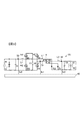
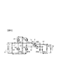
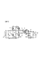
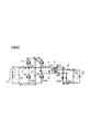
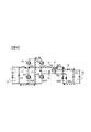
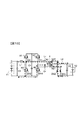
- FIG. 1 is a circuit configuration diagram of a DC-DC converter according to a first embodiment.
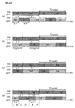
- FIG. (A) (b) (c) (d) It is a time chart which shows on-off of the 1st switching element H1-the 4th switching element H4. It is a circuit block diagram of the DC-DC converter using a current detector. It is a circuit block diagram which shows the example at the time of using a switching element for the rectifier circuit of a DC-DC converter. It is operation
- a third capacitor C3 is connected in parallel with the primary power source V1. Further, the primary power source V1 is connected to a first AC connection portion of a bridge circuit described later via a first inductor L1.
- the bridge circuit includes a first arm in which a first switching element H1 and a second switching element H2 are connected in series via a first AC connection portion, and a second switching element H3 and a fourth switching element H4.
- the second arm is connected in series via an AC connection.
- a first capacitor C1 is connected in parallel to the first arm and the second arm.
- Diodes DH1 to DH4 are connected in reverse parallel to the first switching element H1 to the fourth switching element H4, respectively.
- MOSFET body diodes can be used instead of the diodes DH1 to DH4.
- the first AC connection of the first arm is connected to one end of the primary winding N1 of the transformer 4 via the resonant inductor Lr, and the second AC connection of the second arm is connected to the transformer 4 via the transformer capacitor Cr. Is connected to the other end of the primary winding N1.
- the transformer 4 magnetically couples the primary winding N1 and the secondary windings N21 and N22.
- Diodes DS1 and DS2 constituting a rectifier circuit are connected to both ends of the secondary windings N21 and N22.
- An intermediate point between the secondary windings N21 and N22 is connected to the secondary power source V2 via the second inductor L2.
- a second capacitor C2 is connected to the output side of the rectifier circuit in parallel with the secondary power supply V2.
- the first voltage detector 21 for detecting the voltage value Vc1 of the first capacitor C1 is connected to the connection point between the first arm and the second arm.
- a third voltage detector 23 for detecting a voltage value Vc3 of the third capacitor C3 is connected to a connection point between the first inductor L1 and the primary power supply V1.
- the first voltage detector 21 and the third voltage detector 23 are connected to the control circuit 40.
- the control circuit 40 controls the switching elements of the first arm and the second arm, as will be described later, based on the voltage value detected by each voltage detector.
- a second voltage detector for detecting the voltage value Vc2 of the second capacitor C2 is connected to the connection point of the second inductor L2 and the secondary power source V2, and the control circuit 40 is detected by the second voltage detector. Based on the voltage value Vc2, the switching elements of the first arm and the second arm may be controlled as described later.
- the control circuit 40 controls each switching element H1 to H4 of the bridge circuit to which the primary power supply V1 that is a DC power supply is applied, and 1 of the transformer 4 An AC voltage is applied to the next winding N1.
- the voltage applied to the first capacitor C1 is higher than the voltage of the primary power supply V1 by the booster circuit including the first inductor L1, the first capacitor C1, and the first arm.
- the induced voltage generated in the secondary windings N21 and N22 of the transformer 4 is rectified by a rectifier circuit, and power is supplied to the secondary power source V2.
- the control circuit 40 includes a cycle control circuit 41, a cycle limit circuit 42, a phase difference control circuit 43, and a phase difference limit circuit 44.
- the cycle control circuit 41 receives the voltage value Vc3 from the third voltage detector 23, and adjusts the voltage value Vc1 of the first capacitor C1 to a desired voltage value from a host controller or control circuit 40 (not shown).
- a voltage command value Vc1_ref is input.
- the cycle control circuit 41 calculates the cycle time width ⁇ 1 of the first switching element H1 and the cycle time width ⁇ 2 of the second switching element H2 by the following equations (1) and (2).
- the cycle time widths ⁇ 1 and ⁇ 2 calculated by the cycle control circuit 41 are input to the cycle limit circuit 42.
- the period limit circuit 42 is further input with a time width limit value ⁇ _limit, and limits the value so that the period time widths ⁇ 1 and ⁇ 2 do not exceed the time width limit value ⁇ _limit. This is for preventing the overvoltage from being applied to the switching element or the like by the cycle time widths ⁇ 1, ⁇ 2 exceeding the time width limit value ⁇ _limit.
- the control circuit 40 controls on / off of the first switching element H1 to the fourth switching element H4 as shown in FIG. 2A based on the period time widths ⁇ 1, ⁇ 2 output from the period limiting circuit 42. As a result, the voltage value Vc1 of the first capacitor C1 is adjusted to coincide with the voltage command value Vc1_ref.
- the voltage value Vc1 is input from the first voltage detector 21 to the phase difference control circuit 43, and the voltage value Vc2 of the second capacitor C2 is changed to a desired voltage value from the host controller or the control circuit 40 (not shown).
- a voltage command value Vc2_ref for adjustment is input.
- the phase difference control circuit 43 calculates the phase difference (superimposition time width) ⁇ 1 between the first switching element H1 and the fourth switching element H4, the second switching element H2 and the third switching element H3 by the following equation (3).
- the phase difference (superimposition time width) ⁇ 2 is calculated.
- N is the turn ratio of the transformer 4
- N (N21 + N22) / N1.
- phase differences ⁇ 1 and ⁇ 2 calculated by the phase difference control circuit 43 are input to the phase difference limiting circuit 44.
- a phase difference limit value ⁇ _limit is input to the phase difference limit circuit 44, and the value is limited so that the phase differences ⁇ 1 and ⁇ 2 do not exceed the phase difference limit value ⁇ _limit. This is to limit the phase differences ⁇ 1 and ⁇ 2 so as not to exceed the period time widths ⁇ 1 and ⁇ 2.
- the control circuit 40 controls on / off of the first switching element H1 to the fourth switching element H4 based on the phase differences ⁇ 1 and ⁇ 2 output from the phase difference limiting circuit 44, as shown in FIG. As a result, the voltage value Vc2 of the second capacitor C2 is adjusted to coincide with the voltage command value Vc2_ref.
- the output power of the DC-DC converter 101 is determined by the voltage time product to the primary winding N1 of the transformer 4. Accordingly, the phase difference (superimposition time width) ⁇ 1 of the on-time between the first switching element H1 and the fourth switching element H4 or the phase difference (superimposition time width) ⁇ 2 of the on-time between the second switching element H2 and the third switching element H3 is When the period time width ⁇ 1 of the first switching element H1 and the third switching element H3 and the period time width ⁇ 2 of the second switching element H2 and the fourth switching element H4 are equal to the smaller period time width, the DC-DC converter 101 The maximum output is obtained (see FIG. 2B described later). When the phase difference exceeds the maximum value, the output power of the DC-DC converter 101 does not increase even if the phase difference is increased. Therefore, limit control is performed on the phase difference with the phase difference limit value ⁇ _limit.
- the on-time phase difference (superimposition time width) ⁇ 1 between the first switching element H1 and the fourth switching element H4 and the on-time phase difference (superimposition time width) ⁇ 2 between the second switching element H2 and the third switching element H3 are: It is equal to the time width of the voltage for each polarity applied to the primary winding N1 of the transformer 4.
- the time widths ⁇ 1 and ⁇ 2 of the voltage applied to the primary winding N1 of the transformer 4 are different, the voltage-time product of the primary winding N1 of the transformer 4 varies depending on the polarity. May cause saturation.
- the on-time phase difference ⁇ 1 of the first switching element H1 and the fourth switching element H4 and the on-time phase difference ⁇ 2 of the second switching element H2 and the third switching element H3 are controlled to be equal to each other. . If there is no problem even if the voltage-time product of the primary winding N1 of the transformer 4 differs depending on the polarity due to the influence of disturbance or the like, the on-time phase difference ⁇ 1 between the first switching element H1 and the fourth switching element H4, The on-time phase difference ⁇ 2 between the second switching element H2 and the third switching element H3 is not necessarily equal.
- FIG. 2B is a time chart showing ON / OFF of the first switching element H1 to the fourth switching element H4 when the output of the DC-DC converter 101 is maximized.
- a command value that maximizes the voltage value Vc2 is input to the phase difference control circuit 43 as the voltage command value Vc2_ref. If the phase differences ⁇ 1 and ⁇ 2 exceed the phase difference limit value ⁇ _limit, the phase differences ⁇ 1 and ⁇ 2 are limited so as not to exceed the period time widths ⁇ 1 and ⁇ 2.
- the control circuit 40 controls on / off of the first switching element H1 to the fourth switching element H4 based on the phase differences ⁇ 1 and ⁇ 2 output from the phase difference limiting circuit 44, as shown in FIG. 2B.
- the time chart shown in FIG. 2A shows that the cycle time width ⁇ 1 of the first switching element H1 and the third switching element H3 of the DC-DC converter 101 is the cycle time width of the second switching element H2 and the fourth switching element H4. This is the case when it is smaller than ⁇ 2.
- the phase difference ⁇ 1 of the on-time of the first switching element H1 and the fourth switching element H4 and the phase difference ⁇ 2 of the on-time of the second switching element H2 and the third switching element H3 are the same as those of the DC-DC converter 101.
- the value is equal to or less than the cycle time width ⁇ 1 of the first switching element H1 and the third switching element H3, and the following equation (4) is satisfied. Under the condition expressed by the equation (4), the voltage value Vc1 is larger than twice the voltage value Vc3. ⁇ 2> ⁇ 1 ⁇ ⁇ 1, ⁇ 2 (4)
- the time chart shown in FIG. 2D shows that the cycle time width ⁇ 1 of the first switching element H1 and the third switching element H3 of the DC-DC converter 101 is equal to the period time width of the second switching element H2 and the fourth switching element H4. This is the case when ⁇ 2 or more. This is realized by inputting a desired voltage command value Vc1_ref to the cycle control circuit 41.
- the phase difference ⁇ 1 between the first switching element H1 and the fourth switching element H4, and the phase difference ⁇ 2 between the second switching element H2 and the third switching element H3 are the second switching element H2 and the second switching element H2 of the DC-DC converter 101.
- the value is equal to or smaller than the cycle time width ⁇ 1 of the four switching elements H4, and the following equation (5) is satisfied.
- the voltage value Vc1 is 1 to 2 times or less of the voltage value Vc3. ⁇ 1 ⁇ ⁇ 2 ⁇ ⁇ 1, ⁇ 2 (5)
- the voltage command value Vc3_ref for adjusting the voltage value Vc1 and the voltage value Vc3 of the third capacitor C3 to a desired voltage value is input to the cycle control circuit 41, and the first equation is obtained by the following equations (6) and (7).
- the voltage value Vc2 and the voltage command value Vc1_ref are input to the phase difference control circuit 43, and the phase difference (superimposition time width) between the first switching element H1 and the fourth switching element H4 by the following equation (8).
- ⁇ 1 and a phase difference (superimposition time width) ⁇ 2 between the second switching element H2 and the third switching element H3 are calculated.
- N is the turn ratio of the transformer 4
- N (N21 + N22) / N1.
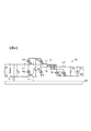
- FIG. 3 is a circuit configuration diagram of a DC-DC converter 101 using a current detector instead of a voltage detector. The same parts as those in FIG. The details of the control circuit 40 are not shown.
- the switching elements H1 to H4 of the first arm and the second arm are controlled based on the current value detected by providing a current detector.
- a first current detector 31 for detecting a current value Ic1 flowing through the primary winding N1 of the transformer 4 is provided.
- a second current detector 32 for detecting a current value Ic2 flowing through the secondary windings N21 and N22 of the transformer 4 is provided.
- a third current detector 33 that detects the current value Ic3 flowing through the first inductor L1 is provided.
- the control circuit 40 obtains the cycle time widths ⁇ 1 and ⁇ 2 and the phase differences ⁇ 1 and ⁇ 2 from the following equations (9) to (11).
- ⁇ 1 (Ic1_ref / Ic3) ⁇ T (9)
- ⁇ 2 (1 ⁇ Ic1_ref / Ic3) ⁇ T (10)
- Ic1_ref is a current command value of a current desired to flow through the primary winding N1 of the transformer 4
- Ic2_ref is a current command value desired to flow through the secondary windings N21 and N22 of the transformer 4.
- the control circuit 40 may use a mixture of the above-described voltage detector and current detector as appropriate. Furthermore, a part may be used without using all of the voltage detector or the current detector.
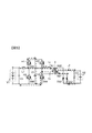
- FIG. 4 is a circuit configuration diagram illustrating an example in which a switching element is used in the rectifier circuit of the DC-DC converter 101. The same parts as those in FIG. The details of the control circuit 40 are not shown.
- the rectifier circuit is composed of diodes DS1 and DS2.
- the switching element S1 and the switching element S2, and the diode DS1 and the diode DS2 are used as the rectifier circuit.
- MOSFETs are used as the switching elements S1 and S2
- the loss can be reduced by diverting the current flowing through the diode DS1 to the switching element S1 if the switching element S1 is turned on.
- FIGS. 5 to 10 are diagrams for explaining the operation of the DC-DC converter 101 in FIG.
- Each of FIGS. 5 to 10 corresponds to phases A to F of the operation of the switching elements H1 to H4 shown in FIG. 2 (d).
- phase A as shown in FIG. 5, the first switching element H1 is in the ON state, the voltage of the primary power supply V1 is not applied to the first inductor L1, and the energy of the first inductor L1 is released. Further, the energy of the primary power supply V1 is stored in the first capacitor C1.
- the fourth switching element H4 is in the ON state, the voltage of the primary power supply V1 is applied to the primary winding N1 of the transformer 4, and the current of the resonant inductor Lr increases. The current flowing through the first capacitor C1 decreases and shifts to phase B when it reaches zero.
- phase B as shown in FIG. 6, the first switching element H1 is in the ON state, the voltage of the primary power supply V1 is not applied to the first inductor L1, and the energy of the first inductor L1 is released. Energy is also released from the first capacitor C1. Further, the fourth switching element H4 is in the ON state, the voltage of the primary power supply V1 is applied to the primary winding N1 of the transformer 4, and the current of the resonant inductor Lr increases. When the fourth switching element H4 is turned off and the third switching element H3 is turned on, the process proceeds to phase C.
- phase C as shown in FIG. 7, the first switching element H1 is in the ON state, the voltage of the primary power supply V1 is not applied to the first inductor L1, and the energy of the first inductor L1 is released. Further, the third switching element H3 is in the on state, and energy is stored in the first capacitor C1. Further, since the voltage of the primary power source V1 is not applied to the primary winding N1 of the transformer 4, the current of the resonant inductor Lr decreases. When the current of the resonant inductor Lr decreases and becomes zero, the phase D is entered.
- phase F as shown in FIG. 10, the second switching element H2 is in the ON state, the voltage of the primary power supply V1 is applied to the first inductor L1, and energy is accumulated in the first inductor L1. Further, the fourth switching element H4 is in the on state, and the energy of the first capacitor C1 is released. Further, since the voltage of the primary power source V1 is not applied to the primary winding N1 of the transformer 4, the current of the resonant inductor Lr decreases.
- the second switching element H2 is turned off and the first switching element H1 is turned on, the process proceeds to phase A. Subsequent operations are repeated from phase A to phase F.
- the voltage applied to the DC-DC converter 101 can be boosted to control the input voltage range, and the booster circuit and the switching element of the DC-DC converter are shared. As a result, the circuit can be reduced in size and cost.
- the motor M is connected to the HV system 102 such as a motor drive inverter, and the HV system 102 is connected to the D side of the DC-DC converter 101.
- Auxiliary equipment 103 such as an air conditioner is connected to the E side of DC-DC converter 101.
- the control circuit 401 controls the switching operation of each of the switching elements H1 to H4 of the DC-DC converter 101, the power transmission direction, the amount of power, and the like. Note that the relay 106 may not be provided.
- FIG. 12 is a circuit configuration diagram of the power supply system according to the present embodiment. Since the circuit configuration of the DC-DC converter 101 is the same as that of the first embodiment, the same portions are denoted by the same reference numerals and the description thereof is omitted.
- the charger 108 includes an AC-DC converter 51 that converts an AC voltage input from the external power supply 109 into a DC voltage.
- a switching circuit 52 is connected to the output side of the AC-DC converter 51 via a fourth capacitor C4 for smoothing.
- the switching circuit 52 is configured by a bridge circuit including four switching elements, and converts a DC voltage into an AC voltage under the control of the control circuit 401.
- the switching circuit 52 is connected to the primary winding side of the transformer 53, and the rectifier circuit 54 is connected to the secondary winding side of the transformer 53.
- the output of the rectifier circuit 54 is connected to both ends of the first capacitor C1 of the DC-DC converter 101.
- the AC-DC converter 51 may have a circuit configuration in which an AC voltage is changed to a DC voltage, such as a circuit configuration in which a bridge rectifier circuit and a boost chopper are combined, or a totem pole circuit. If the external power source 109 is a DC power source, the AC-DC converter 51 can be omitted.
- the switching circuit 52 may be a circuit configuration that converts a DC voltage into an AC voltage, such as a half-bridge circuit, a full-bridge circuit, or a resonance circuit.
- the rectifier circuit 54 may be any circuit configuration that converts AC voltage into DC voltage, such as diode rectification, synchronous rectification, a center tap circuit, or a current doubler system.
- the third voltage detector 23 detects the voltage Vc3 of the third capacitor C3 in order to control the switching time ratio between the element H3 and the fourth switching element H4.
- the detected voltage Vc3 is input to the cycle control circuit 41 of the control circuit 401 together with the target voltage command value Vc1_ref of the first capacitor C1, and the cycle time width ⁇ 1 of the first switching element H1 and the third switching element H3, the first The period time width ⁇ 2 of the second switching element H2 and the fourth switching element H4 is calculated.
- the operations of the cycle control circuit 41 and the cycle limiting circuit 42 are the same as those in the first embodiment, and a description thereof will be omitted.
- the first voltage detector 21 detects the voltage value Vc1 of the first capacitor C1.
- the detected voltage value Vc1 is input to the phase difference control circuit 43 together with the target voltage command value Vc2_ref of the second capacitor C2, the phase difference ⁇ 1 between the first switching element H1 and the fourth switching element H4, and the second switching.
- a phase difference ⁇ 2 between the element H2 and the third switching element H3 is calculated.
- the operations of the phase difference control circuit 43 and the phase difference limiting circuit 44 are the same as in the first embodiment, and a description thereof will be omitted.
- the fourth voltage detector 24 detects the voltage value Vc4 of the fourth capacitor C4.
- the detected voltage value Vc4 is input to the switching control circuit 45 together with the voltage command value Vc1_ref applied to the target DC-DC converter 101, and the control amount ⁇ of the switching circuit 52 is calculated.
- the voltage command value Vc1_ref is input as a command value for designating the voltage value Vc1 of the first capacitor C1 in the DC-DC converter 101 as a desired voltage value from a host controller (not shown) or the control circuit 40.
- the control amount ⁇ calculated by the switching control circuit 45 is compared with the maximum control amount ⁇ _limit of the predetermined switching circuit 52 by the switching limit circuit 46.
- the switching control circuit 45 When the calculated control amount ⁇ does not exceed the maximum control amount ⁇ _limit, the switching control circuit 45 outputs the calculated control amount ⁇ . When the calculated control amount ⁇ exceeds the predetermined maximum control amount ⁇ _limit, the switching limit circuit 46 outputs the maximum control amount ⁇ _limit as the control amount ⁇ . The amount of power is limited by the maximum control amount ⁇ _limit.
- the control circuit 401 controls the switching circuit 52 based on the control amount ⁇ so that the voltage applied to the DC-DC converter 101 becomes the voltage command value Vc1_ref. As described above, by suppressing the output voltage of the rectifier circuit 54 on the output side of the charger 108 to an output voltage range based on the control amount ⁇ , the design flexibility of the charger 108 can be increased.
- the control circuit 401 detects the voltage value Vc4 of the fourth capacitor C4 by the fourth voltage detector 24. However, the control circuit 401 detects the current value flowing to the input side of the switching circuit 52 by the current detector, and uses this current value. May be used to control.
- the DC-DC converter 101 is a DC-DC converter 101 that performs voltage conversion of DC power supplied from the primary power supply V1, and the first switching element H1 and the second switching element H2 are connected to each other by a first AC connection.
- a bridge circuit having a first arm connected in series via a section, and a second arm in which a third switching element H3 and a fourth switching element H4 are connected in series via a second AC connection,
- a booster circuit having an inductor L1 connected between the primary power source V1 and the first AC connection, a first capacitor C1 connected in parallel to the first arm, and the first arm, and one end of the first AC connection.
- the present invention is not limited to the above-described embodiment, and other forms conceivable within the scope of the technical idea of the present invention are also included in the scope of the present invention as long as the characteristics of the present invention are not impaired. .
Landscapes
- Engineering & Computer Science (AREA)
- Power Engineering (AREA)
- Dc-Dc Converters (AREA)
Abstract
本発明の課題は、DC-DCコンバータに追加した昇圧回路の分だけ回路素子が増加し、さらなる小型化、低コスト化の妨げとなることである。 そこで、本発明は、一次電源V1から二次電源V2へ電力を伝送する順送電において、制御回路40は、直流電源である一次電源V1が印加されたブリッジ回路の各スイッチング素子を制御し、トランス4の1次巻線N1に交流電圧を印加する。この場合、第1インダクタL1と第1コンデンサC1と第1アームとを含んで構成される昇圧回路により、第1コンデンサにC1に印加される電圧は、一次電源V1の電圧より高くなる。そして、トランス4の2次巻線N21、N22に生じた誘起電圧を整流回路で整流し、二次電源V2に電力を供給する。このように、昇圧回路と、DC-DCコンバータのスイッチング素子を共用化することで、回路の大型化やコスト増大を抑制できる。
Description
本発明はDC-DCコンバータ、及び自動車に関する。
近年、化石燃料の枯渇や地球環境問題の悪化を背景に、ハイブリッド自動車や電気自動車など、電気エネルギーを利用した自動車への関心が高まっている。
このような電気エネルギーを用いた自動車は、車輪を駆動するためのモータを備え、さらにモータに電力を供給するための高圧バッテリを備えている。そして、この高圧バッテリの出力電圧をDC-DCコンバータにより降圧して、低圧の電気機器へ必要な電力を供給する電源システムを備えている。低圧の電気機器の例として、エアコンやオーディオ、自動車のコントローラー等がある。
このような電気エネルギーを用いた自動車は、車輪を駆動するためのモータを備え、さらにモータに電力を供給するための高圧バッテリを備えている。そして、この高圧バッテリの出力電圧をDC-DCコンバータにより降圧して、低圧の電気機器へ必要な電力を供給する電源システムを備えている。低圧の電気機器の例として、エアコンやオーディオ、自動車のコントローラー等がある。
高圧バッテリには、リチウムイオン電池が用いられることが多い。しかし、リチウムイオン電池の電圧が、十分に足りない場合、DC-DCコンバータを含めた高圧機器に流れる電流量が増加するため、高圧機器の小型化、低コスト化の妨げとなっていた。特許文献1には、高圧バッテリとDC-DCコンバータとの間に、昇圧回路を設けて、高圧バッテリの電圧が低い場合にも、DC-DCコンバータに入力される電圧を昇圧する技術が開示されている。この技術によれば、DC-DCコンバータには、高圧バッテリ電圧よりも高い入力電圧が印加されるため、DC-DCコンバータに流れる電流量が少なくなり、DC-DCコンバータの小型化、低コスト化を図ることが可能である。
特許文献1の技術では、追加した昇圧回路の分だけ回路素子が増加し、さらなる小型化、低コスト化の妨げとなる。
本発明によるDC-DCコンバータは、一次電源から供給される直流電力の電圧変換を行うDC-DCコンバータであって、第1スイッチング素子と第2スイッチング素子とが第1交流接続部を介して直列に接続された第1アームと、第3スイッチング素子と第4スイッチング素子とが第2交流接続部を介して直列に接続された第2アームとを有するブリッジ回路と、前記一次電源と前記第1交流接続部の間に接続されるインダクタと、前記第1アームに並列に接続される第1コンデンサと、前記第1アームとを有する昇圧回路と、一端が前記第1交流接続部に他端が前記第2交流接続部に接続される1次巻線と、前記1次巻線に磁気結合する2次巻線とを有するトランスと、前記トランスの2次巻線側に接続される整流回路と、前記第1アームおよび前記第2アームの各スイッチング素子を制御する制御回路と、を備える。
本発明による自動車は、DC-DCコンバータを含む電源システムを備える。
本発明による自動車は、DC-DCコンバータを含む電源システムを備える。
本発明によれば、小型化、低コスト化が可能なDC-DCコンバータ、さらに、これを用いた自動車を提供することができる。
(第1の実施形態)
以下、図面を参照して、本発明に係る第1の実施形態について説明する。
図1は、第1の実施形態によるDC-DCコンバータ101の回路構成図である。本実施形態におけるDC-DCコンバータ101は、一次電源V1と二次電源V2との間に接続され、一次電源V1と二次電源V2との間で電力の授受を行う。一次電源V1、二次電源V2は共に直流電源であり、それぞれ二次電池により構成される。なお、一次電源V1から二次電源V2へ電力を伝送することを順送電と呼称する。一次電源V1には負荷R1が並列に接続され、二次電源V2には負荷R2が並列に接続されている。
以下、図面を参照して、本発明に係る第1の実施形態について説明する。
図1は、第1の実施形態によるDC-DCコンバータ101の回路構成図である。本実施形態におけるDC-DCコンバータ101は、一次電源V1と二次電源V2との間に接続され、一次電源V1と二次電源V2との間で電力の授受を行う。一次電源V1、二次電源V2は共に直流電源であり、それぞれ二次電池により構成される。なお、一次電源V1から二次電源V2へ電力を伝送することを順送電と呼称する。一次電源V1には負荷R1が並列に接続され、二次電源V2には負荷R2が並列に接続されている。
図1に示すように、一次電源V1と並列に第3コンデンサC3が接続される。また、一次電源V1は第1インダクタL1を介して、後述するブリッジ回路の第1交流接続部に接続される。ブリッジ回路は、第1スイッチング素子H1と第2スイッチング素子H2とが第1交流接続部を介して直列に接続された第1アームと、第3スイッチング素子H3と第4スイッチング素子H4とが第2交流接続部を介して直列に接続された第2アームとにより構成される。第1アームおよび第2アームに並列に第1コンデンサC1が接続される。
第1スイッチング素子H1乃至第4スイッチング素子H4には、それぞれダイオードDH1乃至DH4が逆並列接続されている。なお、第1スイッチング素子H1乃至第4スイッチング素子H4として、Si-MOSFETやSiC-MOSFETを使用した場合は、ダイオードDH1乃至DH4の替わりにMOSFETのボディダイオードを用いることができる。
第1アームの第1交流接続部は、共振インダクタLrを介してトランス4の一次巻線N1の一端に接続され、第2アームの第2交流接続部は、トランス用コンデンサCrを介してトランス4の一次巻線N1の他端に接続される。トランス4は、1次巻線N1と2次巻線N21、N22とを磁気結合している。2次巻線N21、N22の両端には整流回路を構成するダイオードDS1、DS2が接続される。2次巻線N21、N22の中間点は第2インダクタL2を介して二次電源V2に接続される。整流回路の出力側には、二次電源V2と並列に第2コンデンサC2が接続される。
第1アームと第2アームの接続点には、第1コンデンサC1の電圧値Vc1を検出する第1電圧検出器21が接続される。第1インダクタL1と一次電源V1の接続点には、第3コンデンサC3の電圧値Vc3を検出する第3電圧検出器23が接続される。
第1電圧検出器21、第3電圧検出器23は制御回路40に接続される。制御回路40は、各電圧検出器により検出された電圧値に基づいて、後述するように、第1アームおよび第2アームの各スイッチング素子を制御する。なお、第2インダクタL2と二次電源V2の接続点に、第2コンデンサC2の電圧値Vc2を検出する第2電圧検出器を接続し、制御回路40は、第2電圧検出器により検出された電圧値Vc2に基づいて、後述するように、第1アームおよび第2アームの各スイッチング素子を制御してもよい。
一次電源V1から二次電源V2へ電力を伝送する順送電において、制御回路40は、直流電源である一次電源V1が印加されたブリッジ回路の各スイッチング素子H1~H4を制御し、トランス4の1次巻線N1に交流電圧を印加する。この場合、第1インダクタL1と第1コンデンサC1と第1アームとを含んで構成される昇圧回路により、第1コンデンサC1に印加される電圧は、一次電源V1の電圧より高くなる。そして、トランス4の2次巻線N21、N22に生じた誘起電圧を整流回路で整流し、二次電源V2に電力を供給する。このように、昇圧回路と、DC-DCコンバータのスイッチング素子を共用化することで、回路の小型化、低コスト化が可能になる。
制御回路40は、周期制御回路41、周期制限回路42、位相差制御回路43、位相差制限回路44を備えている。
周期制御回路41には、第3電圧検出器23から電圧値Vc3が入力され、また、図示省略した上位制御装置や制御回路40から、第1コンデンサC1の電圧値Vc1を所望の電圧値に調節するための電圧指令値Vc1_refが入力される。周期制御回路41は、以下の式(1)(2)により、第1スイッチング素子H1の周期時間幅τ1と第2スイッチング素子H2の周期時間幅τ2を算出する。
τ1=(Vc3/Vc1_ref)×T (1)
τ2=(1-Vc3/Vc1_ref)×T (2)
ここで、Tは第1スイッチング素子H1と第2スイッチング素子H2がオンオフを繰り返す1周期の時間である。
図2(a)は、DC-DCコンバータ101の順送電時における第1スイッチング素子H1~第4スイッチング素子H4のオンオフの一例を示すタイムチャートである。この図に示すように、周期時間幅τ1は、1周期Tの中で第1スイッチング素子H1がオンしている時間であり、周期時間幅τ2は、第2スイッチング素子H2がオンしている時間である。なお、周期時間幅τ1は、第3スイッチング素子H3がオンしている時間と等しく、周期時間幅τ2は、第4スイッチング素子H4がオンしている時間と等しい。
図1の制御回路40の説明に戻り、周期制御回路41で算出された周期時間幅τ1、τ2は周期制限回路42へ入力される。周期制限回路42には、更に、時間幅制限値τ_limitが入力されており、周期時間幅τ1、τ2が時間幅制限値τ_limitを超えないようにその値を制限している。これは、周期時間幅τ1、τ2が時間幅制限値τ_limitを超えて大きくなることで、スイッチング素子等に過電圧がかかるのを防止する為である。制御回路40は、周期制限回路42より出力された周期時間幅τ1、τ2に基づいて、図2(a)に示すように、第1スイッチング素子H1~第4スイッチング素子H4のオンオフを制御する。これにより、第1コンデンサC1の電圧値Vc1が電圧指令値Vc1_refと一致するように調節される。
位相差制御回路43には、第1電圧検出器21から電圧値Vc1が入力され、また、図示省略した上位制御装置や制御回路40から、第2コンデンサC2の電圧値Vc2を所望の電圧値に調節するための電圧指令値Vc2_refが入力される。位相差制御回路43は、以下の式(3)により、第1スイッチング素子H1と第4スイッチング素子H4との位相差(重畳時間幅)φ1、第2スイッチング素子H2と第3スイッチング素子H3との位相差(重畳時間幅)φ2を算出する。
φ1=φ2=(Vc2_ref/Vc1)×T×N (3)
ここで、Nはトランス4の巻数比であり、N=(N21+N22)/N1である。
φ1=φ2=(Vc2_ref/Vc1)×T×N (3)
ここで、Nはトランス4の巻数比であり、N=(N21+N22)/N1である。
図2(a)に示すように、位相差φ1は、第1スイッチング素子H1がオンしている時間と第4スイッチング素子H4がオンしている時間が重なっている時間であり、位相差φ2は、第2スイッチング素子H2がオンしている時間と第3スイッチング素子H3がオンしている時間が重なっている時間である。この時間の重なりは、第1スイッチング素子H1と第4スイッチング素子H4がオンオフする周期と、第2スイッチング素子H2と第3スイッチング素子H3がオンオフする周期の位相が異なっていることから生じる。
図1の制御回路40の説明に戻り、位相差制御回路43で算出された位相差φ1、φ2は位相差制限回路44へ入力される。位相差制限回路44には、更に、位相差制限値φ_limitが入力されており、位相差φ1、φ2が位相差制限値φ_limitを超えないようにその値を制限している。これは、位相差φ1、φ2が、周期時間幅τ1、τ2以上にならないように制限するためである。制御回路40は、位相差制限回路44より出力された位相差φ1、φ2に基づいて、図2(a)に示すように、第1スイッチング素子H1~第4スイッチング素子H4のオンオフを制御する。これにより、第2コンデンサC2の電圧値Vc2が電圧指令値Vc2_refと一致するように調節される。
DC-DCコンバータ101の出力電力は、トランス4の1次巻線N1への電圧時間積で決定される。従って、第1スイッチング素子H1と第4スイッチング素子H4のオン時間の位相差(重畳時間幅)φ1もしくは第2スイッチング素子H2と第3スイッチング素子H3のオン時間の位相差(重畳時間幅)φ2が、第1スイッチング素子H1および第3スイッチング素子H3の周期時間幅τ1、第2スイッチング素子H2および第4スイッチング素子H4の周期時間幅τ2のうち小さい周期時間幅と等しい時、DC-DCコンバータ101は最大出力となる(後述する図2(b)参照)。位相差が最大値を超えると、位相差を増やしてもDC-DCコンバータ101の出力電力が増加しないため、位相差に対し、位相差制限値φ_limitにより制限制御を行う。
第1スイッチング素子H1と第4スイッチング素子H4のオン時間の位相差(重畳時間幅)φ1と、第2スイッチング素子H2と第3スイッチング素子H3のオン時間の位相差(重畳時間幅)φ2は、トランス4の1次巻線N1に印加される極性ごとの電圧の時間幅とそれぞれ等しい。なお、トランス4の1次巻線N1に印加される電圧の時間幅φ1とφ2が異なる場合、トランス4の1次巻線N1の電圧時間積が極性によって異なることとなるため、トランス4の磁気飽和を招く恐れがある。従って、第1スイッチング素子H1と第4スイッチング素子H4のオン時間の位相差φ1と、第2スイッチング素子H2と第3スイッチング素子H3のオン時間の位相差φ2は等しい値となるように制御される。なお、外乱等の影響によりトランス4の1次巻線N1の電圧時間積が極性によって異なっても問題ない場合、第1スイッチング素子H1と第4スイッチング素子H4のオン時間の位相差φ1と、第2スイッチング素子H2と第3スイッチング素子H3のオン時間の位相差φ2を必ず等しくしなくともよい。
図2(b)は、DC-DCコンバータ101の出力を最大にした場合の第1スイッチング素子H1~第4スイッチング素子H4のオンオフを示すタイムチャートである。この場合は、電圧指令値Vc2_refとして、電圧値Vc2を最大にする指令値が位相差制御回路43に入力される。仮に、位相差φ1、φ2が位相差制限値φ_limitを超えた場合は、位相差φ1、φ2が、周期時間幅τ1、τ2以上にならないように制限される。制御回路40は、位相差制限回路44より出力された位相差φ1、φ2に基づいて、図2(b)に示すように、第1スイッチング素子H1~第4スイッチング素子H4のオンオフを制御する。
図2(c)は、DC-DCコンバータ101の出力を最小にした場合の第1スイッチング素子H1~第4スイッチング素子H4のオンオフを示すタイムチャートである。この場合は、電圧指令値Vc2_refとして、電圧値Vc2を最小にする指令値、すなわち0Vが位相差制御回路43に入力される。制御回路40は、位相差制限回路44より出力された位相差φ1、φ2に基づいて、図2(c)に示すように、第1スイッチング素子H1~第4スイッチング素子H4のオンオフを制御する。この場合は、図2(c)に示すように、位相差φ1、φ2はゼロである。
図2(a)に示すタイムチャートは、DC-DCコンバータ101の第1スイッチング素子H1および第3スイッチング素子H3の周期時間幅τ1が、第2スイッチング素子H2および第4スイッチング素子H4の周期時間幅τ2より小さい場合である。この場合、第1スイッチング素子H1と第4スイッチング素子H4のオン時間の位相差φ1と、第2スイッチング素子H2と第3スイッチング素子H3のオン時間の位相差φ2は、DC-DCコンバータ101の第1スイッチング素子H1および第3スイッチング素子H3の周期時間幅τ1以下の値となり、以下の式(4)の関係となる。この式(4)で示される条件では、電圧値Vc1は電圧値Vc3の2倍より大きくなる。
τ2 >τ1 ≧φ1、 φ2 (4)
τ2 >τ1 ≧φ1、 φ2 (4)
図2(d)に示すタイムチャートは、DC-DCコンバータ101の第1スイッチング素子H1および第3スイッチング素子H3の周期時間幅τ1が、第2スイッチング素子H2および第4スイッチング素子H4の周期時間幅τ2以上の場合である。これは所望の電圧指令値Vc1_refを周期制御回路41へ入力することにより実現される。この場合、第1スイッチング素子H1と第4スイッチング素子H4の位相差φ1と、第2スイッチング素子H2と第3スイッチング素子H3の位相差φ2は、DC-DCコンバータ101の第2スイッチング素子H2および第4スイッチング素子H4の周期時間幅τ1以下の値となり、以下の式(5)の関係となる。この式(5)で示される条件では、電圧値Vc1は電圧値Vc3の1~2倍以下になる。
τ1 ≧τ2 ≧φ1、 φ2 (5)
τ1 ≧τ2 ≧φ1、 φ2 (5)
本実施形態では、第1コンデンサC1の電圧値Vc1を検出する第1電圧検出器21、第3コンデンサC3の電圧値Vc3を検出する第3電圧検出器23を設けた例で説明した。そして、制御回路40は、電圧値Vc3と電圧指令値Vc1_ref、電圧値Vc1と電圧指令値Vc2_refに基づいて、第1アームおよび第2アームの各スイッチング素子を制御した。しかし、これは一例であり、第2コンデンサC2の電圧値Vc2を検出する第2電圧検出器など他の電圧値と電圧指令値を適宜組み合わせて用いることができる。
例えば、周期制御回路41に電圧値Vc1と第3コンデンサC3の電圧値Vc3を所望の電圧値に調節するための電圧指令値Vc3_refを入力し、以下の式(6)(7)により、第1スイッチング素子H1の周期時間幅τ1と第2スイッチング素子H2の周期時間幅τ2を算出する。
τ1=(Vc3_ref/Vc1)×T (6)
τ2=(1-Vc3_ref/Vc1)×T (7)
τ1=(Vc3_ref/Vc1)×T (6)
τ2=(1-Vc3_ref/Vc1)×T (7)
また、例えば、位相差制御回路43に電圧値Vc2と電圧指令値Vc1_refを入力し、以下の式(8)により、第1スイッチング素子H1と第4スイッチング素子H4との位相差(重畳時間幅)φ1、第2スイッチング素子H2と第3スイッチング素子H3との位相差(重畳時間幅)φ2を算出する。
φ1=φ2=(Vc2/Vc1_ref)×T×N (8)
ここで、Nはトランス4の巻数比であり、N=(N21+N22)/N1である。
φ1=φ2=(Vc2/Vc1_ref)×T×N (8)
ここで、Nはトランス4の巻数比であり、N=(N21+N22)/N1である。
図3は電圧検出器の替わりに電流検出器を用いたDC-DCコンバータ101の回路構成図である。図1と同一箇所には同一の符号を付して説明を省略する。また、制御回路40の詳細は図示を省略する。
この例では、電流検出器を設けて検出した電流値に基づいて第1アームおよび第2アームの各スイッチング素子H1~H4を制御する。図3に示すように、トランス4の1次巻線N1に流れる電流値Ic1を検出する第1電流検出器31を設ける。また、トランス4の2次巻線N21、N22に流れる電流値Ic2を検出する第2電流検出器32を設ける。さらに、第1インダクタL1に流れる電流値Ic3を検出する第3電流検出器33を設ける。そして、制御回路40は以下の式(9)~(11)より、周期時間幅τ1、τ2、位相差φ1、φ2を求める。
τ1=(Ic1_ref /Ic3)×T (9)
τ2=(1-Ic1_ref /Ic3)×T (10)
φ1=φ2=(Ic1 /Ic2_ref)×T×N (11)
ここで、Ic1_refはトランス4の1次巻線N1に流したい電流の電流指令値、Ic2_refはトランス4の2次巻線N21、N22に流したい電流指令値である。
なお、制御回路40は上述した電圧検出器と電流検出器を適宜混在して用いてもよい。さらに、電圧検出器もしくは電流検出器の全てを用いることなく、一部を用いてもよい。
図4は、DC-DCコンバータ101の整流回路にスイッチング素子を用いた場合の例を示す回路構成図である。図1と同一箇所には同一の符号を付して説明を省略する。また、制御回路40の詳細は図示を省略する。
図1では、整流回路をダイオードDS1、DS2で構成した。図4では、整流回路として、スイッチング素子S1およびスイッチング素子S2と、ダイオードDS1およびダイオードDS2を用いた。スイッチング素子S1、S2として、MOSFETを用いる場合は、スイッチング素子S1をオン状態とすれば、ダイオードDS1に流れる電流をスイッチング素子S1へ分流することで損失を低減できる。このように、MOSFETと逆並列接続されたダイオード、またはMOSFETのボディダイオードに、ダイオードの順方向電流が流れるとき、このMOSFETをオン状態として損失を低減することを、以後では同期整流と呼称する。制御回路40により、スイッチング素子S1およびスイッチング素子S2を整流動作させる同期整流動作を行う。また、2次巻線N21およびN22以降の整流回路は、センタタップ整流回路方式に限らず、アクティブクランプ付き電流形センタタップ回路やその他、サージ吸収回路、カレントダブラ回路、電流形フルブリッジ回路の組合せでもよい。
図1では、整流回路をダイオードDS1、DS2で構成した。図4では、整流回路として、スイッチング素子S1およびスイッチング素子S2と、ダイオードDS1およびダイオードDS2を用いた。スイッチング素子S1、S2として、MOSFETを用いる場合は、スイッチング素子S1をオン状態とすれば、ダイオードDS1に流れる電流をスイッチング素子S1へ分流することで損失を低減できる。このように、MOSFETと逆並列接続されたダイオード、またはMOSFETのボディダイオードに、ダイオードの順方向電流が流れるとき、このMOSFETをオン状態として損失を低減することを、以後では同期整流と呼称する。制御回路40により、スイッチング素子S1およびスイッチング素子S2を整流動作させる同期整流動作を行う。また、2次巻線N21およびN22以降の整流回路は、センタタップ整流回路方式に限らず、アクティブクランプ付き電流形センタタップ回路やその他、サージ吸収回路、カレントダブラ回路、電流形フルブリッジ回路の組合せでもよい。
図5~図10は、図1におけるDC-DCコンバータ101の順送電時の動作説明図である。図5~図10の各図は、図2(d)に示す各スイッチング素子H1~ H4の動作のフェーズA~Fに対応している。
フェーズAでは、図5に示すように、第1スイッチング素子H1がオン状態であり、一次電源V1の電圧が、第1インダクタL1に印加されず、第1インダクタL1のエネルギーは放出されている。また、第1コンデンサC1には、一次電源V1のエネルギーが蓄えられる。さらに、第4スイッチング素子H4がオン状態であり、一次電源V1の電圧がトランス4の1次巻線N1に印加され、共振インダクタLrの電流は増加していく。第1コンデンサC1に流れる電流は減少していき、零になるとフェーズBに移行する。
フェーズAでは、図5に示すように、第1スイッチング素子H1がオン状態であり、一次電源V1の電圧が、第1インダクタL1に印加されず、第1インダクタL1のエネルギーは放出されている。また、第1コンデンサC1には、一次電源V1のエネルギーが蓄えられる。さらに、第4スイッチング素子H4がオン状態であり、一次電源V1の電圧がトランス4の1次巻線N1に印加され、共振インダクタLrの電流は増加していく。第1コンデンサC1に流れる電流は減少していき、零になるとフェーズBに移行する。
フェーズBでは、図6に示すように、第1スイッチング素子H1がオン状態であり、一次電源V1の電圧が、第1インダクタL1に印加されず、第1インダクタL1のエネルギーは放出されている。また、第1コンデンサC1からも、エネルギーが放出される。さらに、第4スイッチング素子H4がオン状態であり、一次電源V1の電圧がトランス4の1次巻線N1に印加され、共振インダクタLrの電流は増加していく。第4スイッチング素子H4がオフ状態となり、第3スイッチング素子H3がオン状態となるとフェーズCに移行する。
フェーズCでは、図7に示すように、第1スイッチング素子H1がオン状態であり、一次電源V1の電圧が、第1インダクタL1に印加されず、第1インダクタL1のエネルギーは放出される。また、第3スイッチング素子H3がオン状態であり、第1コンデンサC1にエネルギーが蓄えられる。また、一次電源V1の電圧がトランス4の1次巻線N1に印加されないため、共振インダクタLrの電流は減少していく。共振インダクタLrの電流が減少していき、零になるとフェーズDへ移行する。
フェーズDでは、図8に示すように、第1スイッチング素子H1がオン状態であり、一次電源V1の電圧が、第1インダクタL1に印加されず、第1インダクタL1のエネルギーは放出される。また、第3スイッチング素子H3がオン状態であり、第1コンデンサC1のエネルギーが放出される。第1スイッチング素子H1がオフ状態となり、第2スイッチング素子H2がオン状態となるとフェーズEに移行する。
フェーズEでは、図9に示すように、第2スイッチング素子H2がオン状態であり、一次電源V1の電圧が、第1インダクタL1に印加され、第1インダクタL1へエネルギーが蓄積される。また、第3スイッチング素子H3がオン状態であり、第1コンデンサC1のエネルギーが放出される。また、一次電源V1の電圧がトランス4の1次巻線N1に印加されるため、共振インダクタLrの電流は増加していく。第3スイッチング素子H3がオフ状態となり、第4スイッチング素子H4がオン状態となるとフェーズFに移行する。
フェーズFでは、図10に示すように、第2スイッチング素子H2がオン状態であり、一次電源V1の電圧が、第1インダクタL1に印加され、第1インダクタL1へエネルギーが蓄積される。また、第4スイッチング素子H4がオン状態であり、第1コンデンサC1のエネルギーが放出される。また、一次電源V1の電圧がトランス4の1次巻線N1に印加されないため、共振インダクタLrの電流は減少していく。第2スイッチング素子H2がオフ状態となり、第1スイッチング素子H1がオン状態となるとフェーズAに移行する。以降の動作は、フェーズAからフェーズFの繰り返しとなる。
本実施形態によれば、DC-DCコンバータ101に印加される電圧を昇圧し、入力電圧範囲を制御することが可能であり、かつ、昇圧回路と、DC-DCコンバータのスイッチング素子を共用化することで、回路の小型化、低コスト化を図ることができる。
(第2の実施形態)
図11は、第1の実施形態で示したDC-DCコンバータ101を自動車100に適用して場合の電源システムを示す図である。
本実施形態の電源システムは、DC-DCコンバータ101の充電器側をC側、高圧側をD側、低圧側をE側とすると、DC-DCコンバータ101のD側には、高圧バッテリ104がリレー106を介して接続される。DC-DCコンバータ101のE側には、低圧バッテリ105が接続される。外部電源109からの電力を自動車100へ送電する充電器108はDC-DCコンバータ101のC側に接続される。
図11は、第1の実施形態で示したDC-DCコンバータ101を自動車100に適用して場合の電源システムを示す図である。
本実施形態の電源システムは、DC-DCコンバータ101の充電器側をC側、高圧側をD側、低圧側をE側とすると、DC-DCコンバータ101のD側には、高圧バッテリ104がリレー106を介して接続される。DC-DCコンバータ101のE側には、低圧バッテリ105が接続される。外部電源109からの電力を自動車100へ送電する充電器108はDC-DCコンバータ101のC側に接続される。
そして、モータMはモータ駆動用インバータなどのHV系機器102に接続され、HV系機器102はDC-DCコンバータ101のD側に接続される。エアコンなどの補機機器103は、DC-DCコンバータ101のE側に接続される。制御回路401は、DC-DCコンバータ101の各スイッチング素子H1~ H4のスイッチング動作や、電力の送電方向、電力量等を制御する。なお、リレー106はなくてもよい。
図12は、本実施形態による電源システムの回路構成図である。
DC-DCコンバータ101の回路構成は、第1の実施形態と同様であるので、同一箇所には同一の符号を付してその説明を省略する。充電器108は、外部電源109から入力される交流電圧を直流電圧に変換するAC-DCコンバータ51を備えている。AC-DCコンバータ51の出力側には平滑用の第4コンデンサC4を介してスイッチング回路52が接続される。スイッチング回路52は、4個のスイッチング素子によるブリッジ回路で構成され、制御回路401の制御により、直流電圧を交流電圧に変換する。スイッチング回路52は、トランス53の1次巻線側に接続され、トランス53の2次巻線側には整流回路54が接続される。整流回路54の出力は、DC-DCコンバータ101の第1コンデンサC1の両端に接続される。
DC-DCコンバータ101の回路構成は、第1の実施形態と同様であるので、同一箇所には同一の符号を付してその説明を省略する。充電器108は、外部電源109から入力される交流電圧を直流電圧に変換するAC-DCコンバータ51を備えている。AC-DCコンバータ51の出力側には平滑用の第4コンデンサC4を介してスイッチング回路52が接続される。スイッチング回路52は、4個のスイッチング素子によるブリッジ回路で構成され、制御回路401の制御により、直流電圧を交流電圧に変換する。スイッチング回路52は、トランス53の1次巻線側に接続され、トランス53の2次巻線側には整流回路54が接続される。整流回路54の出力は、DC-DCコンバータ101の第1コンデンサC1の両端に接続される。
AC-DCコンバータ51は、ブリッジ整流回路と昇圧チョッパを組み合せた回路構成や、トーテムポール回路など、交流電圧を直流電圧にする回路構成であってもよい。なお、外部電源109が直流電源の場合はAC-DCコンバータ51を省略することができる。スイッチング回路52は、ハーフブリッジ回路やフルブリッジ回路や、共振回路など、直流電圧を交流電圧に変換する変換する回路構成であればよい。整流回路54は、ダイオード整流や同期整流、センタタップ回路や、カレントダブラ方式など、交流電圧を直流電圧に変換する回路構成であればよい。
図12に示すように、DC-DCコンバータ101の第1アームであり、降圧回路A’である第1スイッチング素子H1および第2スイッチング素子H2のスイッチング時間比と、第2アームである第3スイッチング素子H3および第4スイッチング素子H4のスイッチング時間比を制御するために、第3電圧検出器23により第3コンデンサC3の電圧Vc3を検出する。検出された電圧Vc3は、目標とする第1コンデンサC1の電圧指令値Vc1_refと共に制御回路401の周期制御回路41へ入力され、第1スイッチング素子H1および第3スイッチング素子H3の周期時間幅τ1、第2スイッチング素子H2および第4スイッチング素子H4の周期時間幅τ2が算出される。周期制御回路41および周期制限回路42の動作は第1の実施形態と同様であり、その説明を省略する。
図12において、第1電圧検出器21は第1コンデンサC1の電圧値Vc1を検出する。検出された電圧値Vc1は、目標とする第2コンデンサC2の電圧指令値Vc2_refと共に位相差制御回路43に入力され、第1スイッチング素子H1と第4スイッチング素子H4の位相差φ1と、第2スイッチング素子H2と第3スイッチング素子H3の位相差φ2が算出される。位相差制御回路43および位相差制限回路44の動作は第1の実施形態と同様であり、その説明を省略する。
図12において、第4電圧検出器24は第4コンデンサC4の電圧値Vc4を検出する。検出された電圧値Vc4は、目標とするDC-DCコンバータ101に印加される電圧指令値Vc1_refと共にスイッチング制御回路45に入力され、スイッチング回路52の制御量αが算出される。電圧指令値Vc1_refは、図示省略した上位制御装置や制御回路40より、DC-DCコンバータ101における第1コンデンサC1の電圧値Vc1を所望の電圧値に指定する指令値として入力される。スイッチング制御回路45で算出された制御量αは、スイッチング制限回路46で、所定のスイッチング回路52の最大制御量α_limitと比較される。算出された制御量αが最大制御量α_limitを超えない場合、スイッチング制御回路45は算出された制御量αを出力する。算出された制御量αが、所定の最大制御量α_limitを超えた場合、スイッチング制限回路46は最大制御量α_limitを制御量αとして出力する。最大制御量α_limitによって電力量を制限する。制御回路401は、制御量αに基づいてスイッチング回路52を制御して、DC-DCコンバータ101に印加される電圧が電圧指令値Vc1_refになるようにする。このように、充電器108の出力側である整流回路54の出力電圧を制御量αに基づいた出力電圧範囲に抑制することにより、充電器108の設計自由度を増すことが可能である。
なお、制御回路401は、第4電圧検出器24により第4コンデンサC4の電圧値Vc4を検出したが、電流検出器によりスイッチング回路52の入力側に流れる電流値を検出して、この電流値を用いて制御してもよい。
本実施形態によれば、外部電源109の電力は充電器108からDC-DCコンバータ101を介して、直流電源104や直流電源105に電力を送ることが可能となる。この場合、DC-DCコンバータ101に印加される電圧範囲を抑制することが可能であり、かつ降圧回路A’と、DC-DCコンバータ101のスイッチング素子を共用化することで、電源系統の小型化、低コスト化を図ることができる。
以上説明した実施形態によれば、次の作用効果が得られる。
(1)DC-DCコンバータ101は、一次電源V1から供給される直流電力の電圧変換を行うDC-DCコンバータ101であって、第1スイッチング素子H1と第2スイッチング素子H2とが第1交流接続部を介して直列に接続された第1アームと、第3スイッチング素子H3と第4スイッチング素子H4とが第2交流接続部を介して直列に接続された第2アームとを有するブリッジ回路と、一次電源V1と第1交流接続部の間に接続されるインダクタL1と、第1アームに並列に接続される第1コンデンサC1と、第1アームとを有する昇圧回路と、一端が第1交流接続部に他端が第2交流接続部に接続される1次巻線N1と、1次巻線N1に磁気結合する2次巻線N21、N22とを有するトランスと、トランスの2次巻線側N21、N22に接続される整流回路と、第1アームおよび第2アームの各スイッチング素子を制御する制御回路40と、を備える。これにより、小型化、低コスト化が可能なDC-DCコンバータを提供することができる。
自動車は、DC-DCコンバータを含む電源システムを備える。これにより、小型化、低コスト化が可能なDC-DCコンバータ、さらに、これを用いた自動車を提供することができる。
本発明は、上記の実施形態に限定されるものではなく、本発明の特徴を損なわない限り、本発明の技術思想の範囲内で考えられるその他の形態についても、本発明の範囲内に含まれる。
101 DC-DCコンバータ
V1 一次電源
V2 二次電源
R1、R2 負荷
L1 第1インダクタ
L2 第2インダクタ
H1 第1スイッチング素子
H2 第2スイッチング素子
H3 第3スイッチング素子
H4 第4スイッチング素子
C1 第1コンデンサ
C2 第2コンデンサ
C3 第3コンデンサ
C4 第4コンデンサ
4 トランス
DS1、DS2 ダイオード
21 第1電圧検出器
23 第3電圧検出器
40 制御回路
41 周期制御回路
42 周期制限回路
43 位相差制御回路
44 位相差制限回路
100 自動車
104 高圧バッテリ
105 低圧バッテリ
108 充電器
109 外部電源系統
401 制御回路
V1 一次電源
V2 二次電源
R1、R2 負荷
L1 第1インダクタ
L2 第2インダクタ
H1 第1スイッチング素子
H2 第2スイッチング素子
H3 第3スイッチング素子
H4 第4スイッチング素子
C1 第1コンデンサ
C2 第2コンデンサ
C3 第3コンデンサ
C4 第4コンデンサ
4 トランス
DS1、DS2 ダイオード
21 第1電圧検出器
23 第3電圧検出器
40 制御回路
41 周期制御回路
42 周期制限回路
43 位相差制御回路
44 位相差制限回路
100 自動車
104 高圧バッテリ
105 低圧バッテリ
108 充電器
109 外部電源系統
401 制御回路
Claims (16)
- 一次電源から供給される直流電力の電圧変換を行うDC-DCコンバータであって、
第1スイッチング素子と第2スイッチング素子とが第1交流接続部を介して直列に接続された第1アームと、第3スイッチング素子と第4スイッチング素子とが第2交流接続部を介して直列に接続された第2アームとを有するブリッジ回路と、
前記一次電源と前記第1交流接続部の間に接続されるインダクタと、前記第1アームに並列に接続される第1コンデンサと、前記第1アームとを有する昇圧回路と、
一端が前記第1交流接続部に他端が前記第2交流接続部に接続される1次巻線と、前記1次巻線に磁気結合する2次巻線とを有するトランスと、
前記トランスの2次巻線側に接続される整流回路と、
前記第1アームおよび前記第2アームの各スイッチング素子を制御する制御回路と、
を備えたDC-DCコンバータ。 - 請求項1に記載のDC-DCコンバータにおいて、
前記第1コンデンサの電圧値を検出する第1電圧検出器を備え、
前記制御回路は、前記第1電圧検出器で検出された電圧値に基づいて、前記第1アームおよび前記第2アームの各スイッチング素子を制御するDC-DCコンバータ。 - 請求項2に記載のDC-DCコンバータにおいて、
前記一次電源と並列に第3コンデンサを接続し、
前記第3コンデンサの電圧値を検出する第3電圧検出器を備え、
前記制御回路は、前記第3電圧検出器で検出された電圧値に基づいて、前記第1アームおよび前記第2アームの各スイッチング素子を制御するDC-DCコンバータ。 - 請求項3に記載のDC-DCコンバータにおいて、
前記制御回路は、前記第1電圧検出器および前記第3電圧検出器により検出された電圧値に基づいて、前記第1アームの各スイッチング素子と、前記第2アームの各スイッチング素子のオン時間幅を制御するDC-DCコンバータ。 - 請求項3または請求項4に記載のDC-DCコンバータにおいて、
前記制御回路は、前記第1電圧検出器および前記第3電圧検出器により検出された電圧値に基づいて、前記第1アームの各スイッチング素子におけるオン時間に対し、前記第2アームの各スイッチング素子におけるオン時間の位相差を制御するDC-DCコンバータ。 - 請求項1に記載のDC-DCコンバータにおいて、
前記トランスの1次巻線に流れる電流値を検出する第1電流検出器を備え、
前記制御回路は、前記第1電流検出器で検出された電流値に基づいて、前記第1アームおよび前記第2アームの各スイッチング素子を制御するDC-DCコンバータ。 - 請求項6に記載のDC-DCコンバータにおいて、
前記インダクタに流れる電流値を検出する第3電流検出器を備え、
前記制御回路は、前記第3電流検出器で検出された電流値に基づいて、前記第1アームおよび前記第2アームの各スイッチング素子を制御するDC-DCコンバータ。 - 請求項7に記載のDC-DCコンバータにおいて、
前記制御回路は、前記第1電流検出器および前記第3電流検出器により検出された電流値に基づいて、前記第1アームの各スイッチング素子と、前記第2アームの各スイッチング素子のオン時間幅を制御するDC-DCコンバータ。 - 請求項7または請求項8に記載のDC-DCコンバータにおいて、
前記制御回路は、前記第1電流検出器および前記第3電流検出器により検出された電流値に基づいて、前記第1アームの各スイッチング素子におけるオン時間に対し、前記第2アームの各スイッチング素子におけるオン時間の位相差を制御するDC-DCコンバータ。 - 請求項5または請求項9に記載のDC-DCコンバータにおいて、
前記第1アームのスイッチング素子のオン時間幅は、前記第1アームのスイッチング素子のオン時間幅と前記第2アームのスイッチング素子のオン時間幅との重畳時間幅以上であるDC-DCコンバータ。 - 請求項1から請求項10までのいずれか一項に記載のDC-DCコンバータを含む電源システムを備えた自動車。
- 請求項11に記載の自動車において、
前記DC-DCコンバータの前記ブリッジ回路に対して、外部電源からの電力が入力され、
前記一次電源を充電する充電器を並列に接続した自動車。 - 請求項12に記載の自動車において、
前記充電器は、AC-DCコンバータと、DC-ACコンバータと、充電器用トランスと、充電器用整流回路とを備え、交流の前記外部電源からの電力を供給する自動車。 - 請求項13に記載の自動車において、
前記DC-ACコンバータの入力側に平滑コンデンサを備え、
前記制御回路は、前記平滑コンデンサの電圧値に基づいて、前記充電器の前記DC-ACコンバータのスイッチング素子を制御する自動車。 - 請求項12から請求項14までのいずれか一項に記載の自動車において、
前記充電器は、DC-ACコンバータと、充電器用トランスと、充電器用整流回路とを備え、直流の前記外部電源からの電力を供給する自動車。 - 請求項15に記載の自動車において、
前記制御回路は、前記第1コンデンサの電圧値に基づいて、前記充電器の前記DC-ACコンバータのスイッチング素子を制御する自動車。
Applications Claiming Priority (2)
| Application Number | Priority Date | Filing Date | Title |
|---|---|---|---|
| JP2016-201648 | 2016-10-13 | ||
| JP2016201648A JP6750999B2 (ja) | 2016-10-13 | 2016-10-13 | Dc−dcコンバータ、及び自動車 |
Publications (1)
| Publication Number | Publication Date |
|---|---|
| WO2018070185A1 true WO2018070185A1 (ja) | 2018-04-19 |
Family
ID=61905465
Family Applications (1)
| Application Number | Title | Priority Date | Filing Date |
|---|---|---|---|
| PCT/JP2017/033402 Ceased WO2018070185A1 (ja) | 2016-10-13 | 2017-09-15 | Dc-dcコンバータ、及び自動車 |
Country Status (2)
| Country | Link |
|---|---|
| JP (1) | JP6750999B2 (ja) |
| WO (1) | WO2018070185A1 (ja) |
Families Citing this family (1)
| Publication number | Priority date | Publication date | Assignee | Title |
|---|---|---|---|---|
| CN117200587B (zh) * | 2023-11-08 | 2024-02-02 | 中山市宝利金电子有限公司 | 基于直接功率传输的低功率损耗充电桩电路及充电桩 |
Citations (3)
| Publication number | Priority date | Publication date | Assignee | Title |
|---|---|---|---|---|
| JPH10271833A (ja) * | 1996-08-21 | 1998-10-09 | Origin Electric Co Ltd | 昇圧型ブリッジインバータ回路及びその制御方法 |
| JP2013247817A (ja) * | 2012-05-29 | 2013-12-09 | Toyota Industries Corp | 充電器制御システム |
| JP2014036528A (ja) * | 2012-08-09 | 2014-02-24 | Nippon Soken Inc | 絶縁型充電装置 |
-
2016
- 2016-10-13 JP JP2016201648A patent/JP6750999B2/ja active Active
-
2017
- 2017-09-15 WO PCT/JP2017/033402 patent/WO2018070185A1/ja not_active Ceased
Patent Citations (3)
| Publication number | Priority date | Publication date | Assignee | Title |
|---|---|---|---|---|
| JPH10271833A (ja) * | 1996-08-21 | 1998-10-09 | Origin Electric Co Ltd | 昇圧型ブリッジインバータ回路及びその制御方法 |
| JP2013247817A (ja) * | 2012-05-29 | 2013-12-09 | Toyota Industries Corp | 充電器制御システム |
| JP2014036528A (ja) * | 2012-08-09 | 2014-02-24 | Nippon Soken Inc | 絶縁型充電装置 |
Also Published As
| Publication number | Publication date |
|---|---|
| JP6750999B2 (ja) | 2020-09-02 |
| JP2018064385A (ja) | 2018-04-19 |
Similar Documents
| Publication | Publication Date | Title |
|---|---|---|
| US10461553B2 (en) | Power source device | |
| US9425641B2 (en) | Battery charging apparatus | |
| US9209698B2 (en) | Electric power conversion device | |
| US10763754B2 (en) | Power supply device | |
| US7177163B2 (en) | Two-way DC-DC converter | |
| JP5530401B2 (ja) | 電源装置 | |
| JP5968553B2 (ja) | 電力変換装置 | |
| US10541549B2 (en) | Power supply apparatus | |
| KR101769335B1 (ko) | 멀티 토플러지를 이용한 dc/dc 컨버터 | |
| JP6742145B2 (ja) | 双方向dc−dcコンバータ、これを用いた電源システム及び当該電源システムを用いた自動車 | |
| KR102730545B1 (ko) | 차량용 전력 변환 시스템 및 그 제어 방법 | |
| CN105637750A (zh) | 电力变换装置 | |
| JP6102898B2 (ja) | 電力変換装置 | |
| KR20120031131A (ko) | 전원 장치 | |
| WO2021166233A1 (ja) | 電力変換装置、それを含む車両及び制御方法 | |
| WO2015174331A1 (ja) | 電力変換装置 | |
| JP6369509B2 (ja) | 電力変換回路 | |
| KR101548528B1 (ko) | Dc/dc 컨버터 | |
| WO2010143304A1 (ja) | 電源装置 | |
| JP6750999B2 (ja) | Dc−dcコンバータ、及び自動車 | |
| JP6270753B2 (ja) | 電力変換装置 | |
| US11936297B2 (en) | DC-DC converter including first and second coils magnetically coupled such that current flows through second coil in forward direction of diode by mutual induction as current flowing through first coil from intermediate terminal to output terminal increases and vehicle | |
| JP6397871B2 (ja) | 電源システム | |
| JP4361334B2 (ja) | Dc/dcコンバータ | |
| WO2018235438A1 (ja) | Dc-dcコンバータ、これを用いた電源システム及び当該電源システムを用いた自動車 |
Legal Events
| Date | Code | Title | Description |
|---|---|---|---|
| 121 | Ep: the epo has been informed by wipo that ep was designated in this application |
Ref document number: 17859794 Country of ref document: EP Kind code of ref document: A1 |
|
| NENP | Non-entry into the national phase |
Ref country code: DE |
|
| 122 | Ep: pct application non-entry in european phase |
Ref document number: 17859794 Country of ref document: EP Kind code of ref document: A1 |