WO2018070185A1 - Convertisseur continu-continu et automobile - Google Patents
Convertisseur continu-continu et automobile Download PDFInfo
- Publication number
- WO2018070185A1 WO2018070185A1 PCT/JP2017/033402 JP2017033402W WO2018070185A1 WO 2018070185 A1 WO2018070185 A1 WO 2018070185A1 JP 2017033402 W JP2017033402 W JP 2017033402W WO 2018070185 A1 WO2018070185 A1 WO 2018070185A1
- Authority
- WO
- WIPO (PCT)
- Prior art keywords
- converter
- switching element
- arm
- voltage
- circuit
- Prior art date
Links
Images


Classifications
-
- H—ELECTRICITY
- H02—GENERATION; CONVERSION OR DISTRIBUTION OF ELECTRIC POWER
- H02M—APPARATUS FOR CONVERSION BETWEEN AC AND AC, BETWEEN AC AND DC, OR BETWEEN DC AND DC, AND FOR USE WITH MAINS OR SIMILAR POWER SUPPLY SYSTEMS; CONVERSION OF DC OR AC INPUT POWER INTO SURGE OUTPUT POWER; CONTROL OR REGULATION THEREOF
- H02M3/00—Conversion of dc power input into dc power output
- H02M3/22—Conversion of dc power input into dc power output with intermediate conversion into ac
- H02M3/24—Conversion of dc power input into dc power output with intermediate conversion into ac by static converters
- H02M3/28—Conversion of dc power input into dc power output with intermediate conversion into ac by static converters using discharge tubes with control electrode or semiconductor devices with control electrode to produce the intermediate ac
Definitions
- the present invention relates to a DC-DC converter and an automobile.
- An automobile using such electric energy includes a motor for driving wheels, and further includes a high voltage battery for supplying electric power to the motor.
- a power supply system is provided that steps down the output voltage of the high-voltage battery using a DC-DC converter and supplies necessary power to the low-voltage electrical equipment. Examples of low-voltage electrical equipment include air conditioners, audio, and automobile controllers.
- Patent Document 1 discloses a technique for boosting the voltage input to the DC-DC converter even when the voltage of the high-voltage battery is low by providing a booster circuit between the high-voltage battery and the DC-DC converter. ing. According to this technology, an input voltage higher than the high-voltage battery voltage is applied to the DC-DC converter, so the amount of current flowing through the DC-DC converter is reduced, and the DC-DC converter is reduced in size and cost. Can be achieved.
- a DC-DC converter is a DC-DC converter that performs voltage conversion of direct-current power supplied from a primary power supply, wherein a first switching element and a second switching element are connected in series via a first AC connection.
- a bridge circuit having a first arm connected to the first arm, a second arm in which a third switching element and a fourth switching element are connected in series via a second AC connection, the primary power supply, and the first
- An inductor connected between the AC connection parts, a first capacitor connected in parallel to the first arm, and a booster circuit having the first arm; one end of the first AC connection part and the other end
- a transformer having a primary winding connected to the second AC connection, a secondary winding magnetically coupled to the primary winding, and a rectifier circuit connected to the secondary winding side of the transformer;
- the automobile according to the present invention includes a power supply system including a DC-DC converter.
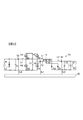
- FIG. 1 is a circuit configuration diagram of a DC-DC converter according to a first embodiment.
- FIG. (A) (b) (c) (d) It is a time chart which shows on-off of the 1st switching element H1-the 4th switching element H4. It is a circuit block diagram of the DC-DC converter using a current detector. It is a circuit block diagram which shows the example at the time of using a switching element for the rectifier circuit of a DC-DC converter. It is operation
- a third capacitor C3 is connected in parallel with the primary power source V1. Further, the primary power source V1 is connected to a first AC connection portion of a bridge circuit described later via a first inductor L1.
- the bridge circuit includes a first arm in which a first switching element H1 and a second switching element H2 are connected in series via a first AC connection portion, and a second switching element H3 and a fourth switching element H4.
- the second arm is connected in series via an AC connection.
- a first capacitor C1 is connected in parallel to the first arm and the second arm.
- Diodes DH1 to DH4 are connected in reverse parallel to the first switching element H1 to the fourth switching element H4, respectively.
- MOSFET body diodes can be used instead of the diodes DH1 to DH4.
- the first AC connection of the first arm is connected to one end of the primary winding N1 of the transformer 4 via the resonant inductor Lr, and the second AC connection of the second arm is connected to the transformer 4 via the transformer capacitor Cr. Is connected to the other end of the primary winding N1.
- the transformer 4 magnetically couples the primary winding N1 and the secondary windings N21 and N22.
- Diodes DS1 and DS2 constituting a rectifier circuit are connected to both ends of the secondary windings N21 and N22.
- An intermediate point between the secondary windings N21 and N22 is connected to the secondary power source V2 via the second inductor L2.
- a second capacitor C2 is connected to the output side of the rectifier circuit in parallel with the secondary power supply V2.
- the first voltage detector 21 for detecting the voltage value Vc1 of the first capacitor C1 is connected to the connection point between the first arm and the second arm.
- a third voltage detector 23 for detecting a voltage value Vc3 of the third capacitor C3 is connected to a connection point between the first inductor L1 and the primary power supply V1.
- the first voltage detector 21 and the third voltage detector 23 are connected to the control circuit 40.
- the control circuit 40 controls the switching elements of the first arm and the second arm, as will be described later, based on the voltage value detected by each voltage detector.
- a second voltage detector for detecting the voltage value Vc2 of the second capacitor C2 is connected to the connection point of the second inductor L2 and the secondary power source V2, and the control circuit 40 is detected by the second voltage detector. Based on the voltage value Vc2, the switching elements of the first arm and the second arm may be controlled as described later.
- the control circuit 40 controls each switching element H1 to H4 of the bridge circuit to which the primary power supply V1 that is a DC power supply is applied, and 1 of the transformer 4 An AC voltage is applied to the next winding N1.
- the voltage applied to the first capacitor C1 is higher than the voltage of the primary power supply V1 by the booster circuit including the first inductor L1, the first capacitor C1, and the first arm.
- the induced voltage generated in the secondary windings N21 and N22 of the transformer 4 is rectified by a rectifier circuit, and power is supplied to the secondary power source V2.
- the control circuit 40 includes a cycle control circuit 41, a cycle limit circuit 42, a phase difference control circuit 43, and a phase difference limit circuit 44.
- the cycle control circuit 41 receives the voltage value Vc3 from the third voltage detector 23, and adjusts the voltage value Vc1 of the first capacitor C1 to a desired voltage value from a host controller or control circuit 40 (not shown).
- a voltage command value Vc1_ref is input.
- the cycle control circuit 41 calculates the cycle time width ⁇ 1 of the first switching element H1 and the cycle time width ⁇ 2 of the second switching element H2 by the following equations (1) and (2).
- the cycle time widths ⁇ 1 and ⁇ 2 calculated by the cycle control circuit 41 are input to the cycle limit circuit 42.
- the period limit circuit 42 is further input with a time width limit value ⁇ _limit, and limits the value so that the period time widths ⁇ 1 and ⁇ 2 do not exceed the time width limit value ⁇ _limit. This is for preventing the overvoltage from being applied to the switching element or the like by the cycle time widths ⁇ 1, ⁇ 2 exceeding the time width limit value ⁇ _limit.
- the control circuit 40 controls on / off of the first switching element H1 to the fourth switching element H4 as shown in FIG. 2A based on the period time widths ⁇ 1, ⁇ 2 output from the period limiting circuit 42. As a result, the voltage value Vc1 of the first capacitor C1 is adjusted to coincide with the voltage command value Vc1_ref.
- the voltage value Vc1 is input from the first voltage detector 21 to the phase difference control circuit 43, and the voltage value Vc2 of the second capacitor C2 is changed to a desired voltage value from the host controller or the control circuit 40 (not shown).
- a voltage command value Vc2_ref for adjustment is input.
- the phase difference control circuit 43 calculates the phase difference (superimposition time width) ⁇ 1 between the first switching element H1 and the fourth switching element H4, the second switching element H2 and the third switching element H3 by the following equation (3).
- the phase difference (superimposition time width) ⁇ 2 is calculated.
- N is the turn ratio of the transformer 4
- N (N21 + N22) / N1.
- phase differences ⁇ 1 and ⁇ 2 calculated by the phase difference control circuit 43 are input to the phase difference limiting circuit 44.
- a phase difference limit value ⁇ _limit is input to the phase difference limit circuit 44, and the value is limited so that the phase differences ⁇ 1 and ⁇ 2 do not exceed the phase difference limit value ⁇ _limit. This is to limit the phase differences ⁇ 1 and ⁇ 2 so as not to exceed the period time widths ⁇ 1 and ⁇ 2.
- the control circuit 40 controls on / off of the first switching element H1 to the fourth switching element H4 based on the phase differences ⁇ 1 and ⁇ 2 output from the phase difference limiting circuit 44, as shown in FIG. As a result, the voltage value Vc2 of the second capacitor C2 is adjusted to coincide with the voltage command value Vc2_ref.
- the output power of the DC-DC converter 101 is determined by the voltage time product to the primary winding N1 of the transformer 4. Accordingly, the phase difference (superimposition time width) ⁇ 1 of the on-time between the first switching element H1 and the fourth switching element H4 or the phase difference (superimposition time width) ⁇ 2 of the on-time between the second switching element H2 and the third switching element H3 is When the period time width ⁇ 1 of the first switching element H1 and the third switching element H3 and the period time width ⁇ 2 of the second switching element H2 and the fourth switching element H4 are equal to the smaller period time width, the DC-DC converter 101 The maximum output is obtained (see FIG. 2B described later). When the phase difference exceeds the maximum value, the output power of the DC-DC converter 101 does not increase even if the phase difference is increased. Therefore, limit control is performed on the phase difference with the phase difference limit value ⁇ _limit.
- the on-time phase difference (superimposition time width) ⁇ 1 between the first switching element H1 and the fourth switching element H4 and the on-time phase difference (superimposition time width) ⁇ 2 between the second switching element H2 and the third switching element H3 are: It is equal to the time width of the voltage for each polarity applied to the primary winding N1 of the transformer 4.
- the time widths ⁇ 1 and ⁇ 2 of the voltage applied to the primary winding N1 of the transformer 4 are different, the voltage-time product of the primary winding N1 of the transformer 4 varies depending on the polarity. May cause saturation.
- the on-time phase difference ⁇ 1 of the first switching element H1 and the fourth switching element H4 and the on-time phase difference ⁇ 2 of the second switching element H2 and the third switching element H3 are controlled to be equal to each other. . If there is no problem even if the voltage-time product of the primary winding N1 of the transformer 4 differs depending on the polarity due to the influence of disturbance or the like, the on-time phase difference ⁇ 1 between the first switching element H1 and the fourth switching element H4, The on-time phase difference ⁇ 2 between the second switching element H2 and the third switching element H3 is not necessarily equal.
- FIG. 2B is a time chart showing ON / OFF of the first switching element H1 to the fourth switching element H4 when the output of the DC-DC converter 101 is maximized.
- a command value that maximizes the voltage value Vc2 is input to the phase difference control circuit 43 as the voltage command value Vc2_ref. If the phase differences ⁇ 1 and ⁇ 2 exceed the phase difference limit value ⁇ _limit, the phase differences ⁇ 1 and ⁇ 2 are limited so as not to exceed the period time widths ⁇ 1 and ⁇ 2.
- the control circuit 40 controls on / off of the first switching element H1 to the fourth switching element H4 based on the phase differences ⁇ 1 and ⁇ 2 output from the phase difference limiting circuit 44, as shown in FIG. 2B.
- the time chart shown in FIG. 2A shows that the cycle time width ⁇ 1 of the first switching element H1 and the third switching element H3 of the DC-DC converter 101 is the cycle time width of the second switching element H2 and the fourth switching element H4. This is the case when it is smaller than ⁇ 2.
- the phase difference ⁇ 1 of the on-time of the first switching element H1 and the fourth switching element H4 and the phase difference ⁇ 2 of the on-time of the second switching element H2 and the third switching element H3 are the same as those of the DC-DC converter 101.
- the value is equal to or less than the cycle time width ⁇ 1 of the first switching element H1 and the third switching element H3, and the following equation (4) is satisfied. Under the condition expressed by the equation (4), the voltage value Vc1 is larger than twice the voltage value Vc3. ⁇ 2> ⁇ 1 ⁇ ⁇ 1, ⁇ 2 (4)
- the time chart shown in FIG. 2D shows that the cycle time width ⁇ 1 of the first switching element H1 and the third switching element H3 of the DC-DC converter 101 is equal to the period time width of the second switching element H2 and the fourth switching element H4. This is the case when ⁇ 2 or more. This is realized by inputting a desired voltage command value Vc1_ref to the cycle control circuit 41.
- the phase difference ⁇ 1 between the first switching element H1 and the fourth switching element H4, and the phase difference ⁇ 2 between the second switching element H2 and the third switching element H3 are the second switching element H2 and the second switching element H2 of the DC-DC converter 101.
- the value is equal to or smaller than the cycle time width ⁇ 1 of the four switching elements H4, and the following equation (5) is satisfied.
- the voltage value Vc1 is 1 to 2 times or less of the voltage value Vc3. ⁇ 1 ⁇ ⁇ 2 ⁇ ⁇ 1, ⁇ 2 (5)
- the voltage command value Vc3_ref for adjusting the voltage value Vc1 and the voltage value Vc3 of the third capacitor C3 to a desired voltage value is input to the cycle control circuit 41, and the first equation is obtained by the following equations (6) and (7).
- the voltage value Vc2 and the voltage command value Vc1_ref are input to the phase difference control circuit 43, and the phase difference (superimposition time width) between the first switching element H1 and the fourth switching element H4 by the following equation (8).
- ⁇ 1 and a phase difference (superimposition time width) ⁇ 2 between the second switching element H2 and the third switching element H3 are calculated.
- N is the turn ratio of the transformer 4
- N (N21 + N22) / N1.
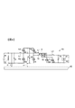
- FIG. 3 is a circuit configuration diagram of a DC-DC converter 101 using a current detector instead of a voltage detector. The same parts as those in FIG. The details of the control circuit 40 are not shown.
- the switching elements H1 to H4 of the first arm and the second arm are controlled based on the current value detected by providing a current detector.
- a first current detector 31 for detecting a current value Ic1 flowing through the primary winding N1 of the transformer 4 is provided.
- a second current detector 32 for detecting a current value Ic2 flowing through the secondary windings N21 and N22 of the transformer 4 is provided.
- a third current detector 33 that detects the current value Ic3 flowing through the first inductor L1 is provided.
- the control circuit 40 obtains the cycle time widths ⁇ 1 and ⁇ 2 and the phase differences ⁇ 1 and ⁇ 2 from the following equations (9) to (11).
- ⁇ 1 (Ic1_ref / Ic3) ⁇ T (9)
- ⁇ 2 (1 ⁇ Ic1_ref / Ic3) ⁇ T (10)
- Ic1_ref is a current command value of a current desired to flow through the primary winding N1 of the transformer 4
- Ic2_ref is a current command value desired to flow through the secondary windings N21 and N22 of the transformer 4.
- the control circuit 40 may use a mixture of the above-described voltage detector and current detector as appropriate. Furthermore, a part may be used without using all of the voltage detector or the current detector.
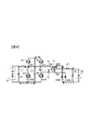
- FIG. 4 is a circuit configuration diagram illustrating an example in which a switching element is used in the rectifier circuit of the DC-DC converter 101. The same parts as those in FIG. The details of the control circuit 40 are not shown.
- the rectifier circuit is composed of diodes DS1 and DS2.
- the switching element S1 and the switching element S2, and the diode DS1 and the diode DS2 are used as the rectifier circuit.
- MOSFETs are used as the switching elements S1 and S2
- the loss can be reduced by diverting the current flowing through the diode DS1 to the switching element S1 if the switching element S1 is turned on.
- FIGS. 5 to 10 are diagrams for explaining the operation of the DC-DC converter 101 in FIG.
- Each of FIGS. 5 to 10 corresponds to phases A to F of the operation of the switching elements H1 to H4 shown in FIG. 2 (d).
- phase A as shown in FIG. 5, the first switching element H1 is in the ON state, the voltage of the primary power supply V1 is not applied to the first inductor L1, and the energy of the first inductor L1 is released. Further, the energy of the primary power supply V1 is stored in the first capacitor C1.
- the fourth switching element H4 is in the ON state, the voltage of the primary power supply V1 is applied to the primary winding N1 of the transformer 4, and the current of the resonant inductor Lr increases. The current flowing through the first capacitor C1 decreases and shifts to phase B when it reaches zero.
- phase B as shown in FIG. 6, the first switching element H1 is in the ON state, the voltage of the primary power supply V1 is not applied to the first inductor L1, and the energy of the first inductor L1 is released. Energy is also released from the first capacitor C1. Further, the fourth switching element H4 is in the ON state, the voltage of the primary power supply V1 is applied to the primary winding N1 of the transformer 4, and the current of the resonant inductor Lr increases. When the fourth switching element H4 is turned off and the third switching element H3 is turned on, the process proceeds to phase C.
- phase C as shown in FIG. 7, the first switching element H1 is in the ON state, the voltage of the primary power supply V1 is not applied to the first inductor L1, and the energy of the first inductor L1 is released. Further, the third switching element H3 is in the on state, and energy is stored in the first capacitor C1. Further, since the voltage of the primary power source V1 is not applied to the primary winding N1 of the transformer 4, the current of the resonant inductor Lr decreases. When the current of the resonant inductor Lr decreases and becomes zero, the phase D is entered.
- phase F as shown in FIG. 10, the second switching element H2 is in the ON state, the voltage of the primary power supply V1 is applied to the first inductor L1, and energy is accumulated in the first inductor L1. Further, the fourth switching element H4 is in the on state, and the energy of the first capacitor C1 is released. Further, since the voltage of the primary power source V1 is not applied to the primary winding N1 of the transformer 4, the current of the resonant inductor Lr decreases.
- the second switching element H2 is turned off and the first switching element H1 is turned on, the process proceeds to phase A. Subsequent operations are repeated from phase A to phase F.
- the voltage applied to the DC-DC converter 101 can be boosted to control the input voltage range, and the booster circuit and the switching element of the DC-DC converter are shared. As a result, the circuit can be reduced in size and cost.
- the motor M is connected to the HV system 102 such as a motor drive inverter, and the HV system 102 is connected to the D side of the DC-DC converter 101.
- Auxiliary equipment 103 such as an air conditioner is connected to the E side of DC-DC converter 101.
- the control circuit 401 controls the switching operation of each of the switching elements H1 to H4 of the DC-DC converter 101, the power transmission direction, the amount of power, and the like. Note that the relay 106 may not be provided.
- FIG. 12 is a circuit configuration diagram of the power supply system according to the present embodiment. Since the circuit configuration of the DC-DC converter 101 is the same as that of the first embodiment, the same portions are denoted by the same reference numerals and the description thereof is omitted.
- the charger 108 includes an AC-DC converter 51 that converts an AC voltage input from the external power supply 109 into a DC voltage.
- a switching circuit 52 is connected to the output side of the AC-DC converter 51 via a fourth capacitor C4 for smoothing.
- the switching circuit 52 is configured by a bridge circuit including four switching elements, and converts a DC voltage into an AC voltage under the control of the control circuit 401.
- the switching circuit 52 is connected to the primary winding side of the transformer 53, and the rectifier circuit 54 is connected to the secondary winding side of the transformer 53.
- the output of the rectifier circuit 54 is connected to both ends of the first capacitor C1 of the DC-DC converter 101.
- the AC-DC converter 51 may have a circuit configuration in which an AC voltage is changed to a DC voltage, such as a circuit configuration in which a bridge rectifier circuit and a boost chopper are combined, or a totem pole circuit. If the external power source 109 is a DC power source, the AC-DC converter 51 can be omitted.
- the switching circuit 52 may be a circuit configuration that converts a DC voltage into an AC voltage, such as a half-bridge circuit, a full-bridge circuit, or a resonance circuit.
- the rectifier circuit 54 may be any circuit configuration that converts AC voltage into DC voltage, such as diode rectification, synchronous rectification, a center tap circuit, or a current doubler system.
- the third voltage detector 23 detects the voltage Vc3 of the third capacitor C3 in order to control the switching time ratio between the element H3 and the fourth switching element H4.
- the detected voltage Vc3 is input to the cycle control circuit 41 of the control circuit 401 together with the target voltage command value Vc1_ref of the first capacitor C1, and the cycle time width ⁇ 1 of the first switching element H1 and the third switching element H3, the first The period time width ⁇ 2 of the second switching element H2 and the fourth switching element H4 is calculated.
- the operations of the cycle control circuit 41 and the cycle limiting circuit 42 are the same as those in the first embodiment, and a description thereof will be omitted.
- the first voltage detector 21 detects the voltage value Vc1 of the first capacitor C1.
- the detected voltage value Vc1 is input to the phase difference control circuit 43 together with the target voltage command value Vc2_ref of the second capacitor C2, the phase difference ⁇ 1 between the first switching element H1 and the fourth switching element H4, and the second switching.
- a phase difference ⁇ 2 between the element H2 and the third switching element H3 is calculated.
- the operations of the phase difference control circuit 43 and the phase difference limiting circuit 44 are the same as in the first embodiment, and a description thereof will be omitted.
- the fourth voltage detector 24 detects the voltage value Vc4 of the fourth capacitor C4.
- the detected voltage value Vc4 is input to the switching control circuit 45 together with the voltage command value Vc1_ref applied to the target DC-DC converter 101, and the control amount ⁇ of the switching circuit 52 is calculated.
- the voltage command value Vc1_ref is input as a command value for designating the voltage value Vc1 of the first capacitor C1 in the DC-DC converter 101 as a desired voltage value from a host controller (not shown) or the control circuit 40.
- the control amount ⁇ calculated by the switching control circuit 45 is compared with the maximum control amount ⁇ _limit of the predetermined switching circuit 52 by the switching limit circuit 46.
- the switching control circuit 45 When the calculated control amount ⁇ does not exceed the maximum control amount ⁇ _limit, the switching control circuit 45 outputs the calculated control amount ⁇ . When the calculated control amount ⁇ exceeds the predetermined maximum control amount ⁇ _limit, the switching limit circuit 46 outputs the maximum control amount ⁇ _limit as the control amount ⁇ . The amount of power is limited by the maximum control amount ⁇ _limit.
- the control circuit 401 controls the switching circuit 52 based on the control amount ⁇ so that the voltage applied to the DC-DC converter 101 becomes the voltage command value Vc1_ref. As described above, by suppressing the output voltage of the rectifier circuit 54 on the output side of the charger 108 to an output voltage range based on the control amount ⁇ , the design flexibility of the charger 108 can be increased.
- the control circuit 401 detects the voltage value Vc4 of the fourth capacitor C4 by the fourth voltage detector 24. However, the control circuit 401 detects the current value flowing to the input side of the switching circuit 52 by the current detector, and uses this current value. May be used to control.
- the DC-DC converter 101 is a DC-DC converter 101 that performs voltage conversion of DC power supplied from the primary power supply V1, and the first switching element H1 and the second switching element H2 are connected to each other by a first AC connection.
- a bridge circuit having a first arm connected in series via a section, and a second arm in which a third switching element H3 and a fourth switching element H4 are connected in series via a second AC connection,
- a booster circuit having an inductor L1 connected between the primary power source V1 and the first AC connection, a first capacitor C1 connected in parallel to the first arm, and the first arm, and one end of the first AC connection.
- the present invention is not limited to the above-described embodiment, and other forms conceivable within the scope of the technical idea of the present invention are also included in the scope of the present invention as long as the characteristics of the present invention are not impaired. .
Landscapes
- Engineering & Computer Science (AREA)
- Power Engineering (AREA)
- Dc-Dc Converters (AREA)
Abstract
La présente invention aborde le problème selon lequel des éléments de circuit sont augmentés d'un nombre égal à ceux d'un circuit survolteur ajouté à un convertisseur continu-continu, le problème constituant un obstacle pour réduire davantage la taille et le coût. Par conséquent, selon la présente invention, pendant la transmission de puissance directe destinée à transmettre de l'énergie d'une alimentation électrique primaire V1 à une alimentation électrique secondaire V2, un circuit de commande 40 commande chacun des éléments de commutation d'un circuit en pont auquel l'alimentation électrique primaire V1, une alimentation électrique en courant continu est appliquée pour appliquer une tension alternative à l'enroulement primaire N1 d'un transformateur 4. Dans ce cas, en raison d'un circuit survolteur comprenant une première bobine d'induction L1, un premier condensateur C1, et un premier bras, la tension appliquée au premier condensateur C1 devient supérieure à la tension de l'alimentation électrique primaire V1. Une tension induite générée dans les enroulements secondaires N21, N22 du transformateur 4 est redressée par un circuit redresseur pour fournir de l'énergie à l'alimentation électrique secondaire V2. De cette manière, les éléments de commutation du convertisseur continu-continu sont partagés avec le circuit survolteur, ce qui permet d'empêcher la taille d'un circuit et le coût d'augmenter.
Applications Claiming Priority (2)
| Application Number | Priority Date | Filing Date | Title |
|---|---|---|---|
| JP2016201648A JP6750999B2 (ja) | 2016-10-13 | 2016-10-13 | Dc−dcコンバータ、及び自動車 |
| JP2016-201648 | 2016-10-13 |
Publications (1)
| Publication Number | Publication Date |
|---|---|
| WO2018070185A1 true WO2018070185A1 (fr) | 2018-04-19 |
Family
ID=61905465
Family Applications (1)
| Application Number | Title | Priority Date | Filing Date |
|---|---|---|---|
| PCT/JP2017/033402 WO2018070185A1 (fr) | 2016-10-13 | 2017-09-15 | Convertisseur continu-continu et automobile |
Country Status (2)
| Country | Link |
|---|---|
| JP (1) | JP6750999B2 (fr) |
| WO (1) | WO2018070185A1 (fr) |
Families Citing this family (1)
| Publication number | Priority date | Publication date | Assignee | Title |
|---|---|---|---|---|
| CN117200587B (zh) * | 2023-11-08 | 2024-02-02 | 中山市宝利金电子有限公司 | 基于直接功率传输的低功率损耗充电桩电路及充电桩 |
Citations (3)
| Publication number | Priority date | Publication date | Assignee | Title |
|---|---|---|---|---|
| JPH10271833A (ja) * | 1996-08-21 | 1998-10-09 | Origin Electric Co Ltd | 昇圧型ブリッジインバータ回路及びその制御方法 |
| JP2013247817A (ja) * | 2012-05-29 | 2013-12-09 | Toyota Industries Corp | 充電器制御システム |
| JP2014036528A (ja) * | 2012-08-09 | 2014-02-24 | Nippon Soken Inc | 絶縁型充電装置 |
-
2016
- 2016-10-13 JP JP2016201648A patent/JP6750999B2/ja active Active
-
2017
- 2017-09-15 WO PCT/JP2017/033402 patent/WO2018070185A1/fr active Application Filing
Patent Citations (3)
| Publication number | Priority date | Publication date | Assignee | Title |
|---|---|---|---|---|
| JPH10271833A (ja) * | 1996-08-21 | 1998-10-09 | Origin Electric Co Ltd | 昇圧型ブリッジインバータ回路及びその制御方法 |
| JP2013247817A (ja) * | 2012-05-29 | 2013-12-09 | Toyota Industries Corp | 充電器制御システム |
| JP2014036528A (ja) * | 2012-08-09 | 2014-02-24 | Nippon Soken Inc | 絶縁型充電装置 |
Also Published As
| Publication number | Publication date |
|---|---|
| JP2018064385A (ja) | 2018-04-19 |
| JP6750999B2 (ja) | 2020-09-02 |
Similar Documents
| Publication | Publication Date | Title |
|---|---|---|
| US10461553B2 (en) | Power source device | |
| US9425641B2 (en) | Battery charging apparatus | |
| US7177163B2 (en) | Two-way DC-DC converter | |
| US10541549B2 (en) | Power supply apparatus | |
| US9787199B2 (en) | Power conversion device to control power distribution of input power to multiple outputs | |
| US10763754B2 (en) | Power supply device | |
| US9209698B2 (en) | Electric power conversion device | |
| JP6102898B2 (ja) | 電力変換装置 | |
| KR20120031131A (ko) | 전원 장치 | |
| JP6742145B2 (ja) | 双方向dc−dcコンバータ、これを用いた電源システム及び当該電源システムを用いた自動車 | |
| JP2006081263A (ja) | 双方向dc−dcコンバータ | |
| JP6369509B2 (ja) | 電力変換回路 | |
| WO2010143304A1 (fr) | Dispositif d'alimentation électrique | |
| WO2018070185A1 (fr) | Convertisseur continu-continu et automobile | |
| JP6397871B2 (ja) | 電源システム | |
| JP6270753B2 (ja) | 電力変換装置 | |
| KR101769335B1 (ko) | 멀티 토플러지를 이용한 dc/dc 컨버터 | |
| WO2018235438A1 (fr) | Convertisseur cc-cc, système d'alimentation électrique utilisant le convertisseur cc-cc, et automobile utilisant le système d'alimentation électrique | |
| JP4361334B2 (ja) | Dc/dcコンバータ | |
| KR101548528B1 (ko) | Dc/dc 컨버터 | |
| US11936297B2 (en) | DC-DC converter including first and second coils magnetically coupled such that current flows through second coil in forward direction of diode by mutual induction as current flowing through first coil from intermediate terminal to output terminal increases and vehicle | |
| WO2021166233A1 (fr) | Dispositif de conversion de puissance, véhicule le comportant et procédé de commande | |
| Huang et al. | Combination of class E inverters with DC-DC converters for a circuit design with controllable dual outputs |
Legal Events
| Date | Code | Title | Description |
|---|---|---|---|
| 121 | Ep: the epo has been informed by wipo that ep was designated in this application |
Ref document number: 17859794 Country of ref document: EP Kind code of ref document: A1 |
|
| NENP | Non-entry into the national phase |
Ref country code: DE |
|
| 122 | Ep: pct application non-entry in european phase |
Ref document number: 17859794 Country of ref document: EP Kind code of ref document: A1 |