WO2018070036A1 - データ作成装置およびデータ作成プログラム - Google Patents
データ作成装置およびデータ作成プログラム Download PDFInfo
- Publication number
- WO2018070036A1 WO2018070036A1 PCT/JP2016/080538 JP2016080538W WO2018070036A1 WO 2018070036 A1 WO2018070036 A1 WO 2018070036A1 JP 2016080538 W JP2016080538 W JP 2016080538W WO 2018070036 A1 WO2018070036 A1 WO 2018070036A1
- Authority
- WO
- WIPO (PCT)
- Prior art keywords
- lead
- data
- pair
- bending
- bending direction
- Prior art date
- Legal status (The legal status is an assumption and is not a legal conclusion. Google has not performed a legal analysis and makes no representation as to the accuracy of the status listed.)
- Ceased
Links
Images






Classifications
-
- H—ELECTRICITY
- H05—ELECTRIC TECHNIQUES NOT OTHERWISE PROVIDED FOR
- H05K—PRINTED CIRCUITS; CASINGS OR CONSTRUCTIONAL DETAILS OF ELECTRIC APPARATUS; MANUFACTURE OF ASSEMBLAGES OF ELECTRICAL COMPONENTS
- H05K13/00—Apparatus or processes specially adapted for manufacturing or adjusting assemblages of electric components
- H05K13/04—Mounting of components, e.g. of leadless components
-
- H—ELECTRICITY
- H05—ELECTRIC TECHNIQUES NOT OTHERWISE PROVIDED FOR
- H05K—PRINTED CIRCUITS; CASINGS OR CONSTRUCTIONAL DETAILS OF ELECTRIC APPARATUS; MANUFACTURE OF ASSEMBLAGES OF ELECTRICAL COMPONENTS
- H05K3/00—Apparatus or processes for manufacturing printed circuits
Definitions
- the present invention relates to a data creation apparatus and a data creation program related to board insertion of lead parts.
- Patent Document 1 describes a technology that supports setting by clearly indicating a prohibited area for placement of electronic components in consideration of an insertion process for inserting a lead component (insertable component) into a substrate. Yes.
- Patent Document 1 describes an example in which a lead wire is bent inward of a lead component along a direction in which two lands of the lead component are arranged.
- a mounting apparatus that can bend a lead of a lead component in a direction different from the above has been proposed.
- a mounting apparatus that inserts lead components into a substrate and subsequently cuts and bends the lead wires generally operates based on NC data.
- the NC data is created based on design information including an arrangement position of an electronic component such as a lead component on the board, a component name of the electronic component, and the like.
- design information regarding the bending direction of the lead wire may not be supplied when creating NC data. In this case, it is necessary to create NC data with the lead bending direction as the optimum direction.
- the present invention has been made in view of the above-described problems, and an object of the present invention is to provide a data creation device that sets the lead bending direction of a lead component to an optimum direction.
- the data creation device is an NC used in a cut and clinching device that cuts and bends the lead of the lead component mounted on the substrate by inserting the lead into the hole provided in the substrate.
- a data creation device for creating data comprising: a determination unit that determines a bending direction of a lead of a lead component based on wiring pattern information of a substrate. In this way, the data creation device can set the lead bending direction of the lead component to an optimum direction.
- the determining means has a bending direction that is a first direction in which the pair of leads of the lead component are arranged, the first bending direction and the first direction in which the pair of leads approach, One of the second bending directions in which the pair of leads are separated or the second bending direction in which the pair of leads are separated is a second direction different from the first direction.
- the data creation device can set the bending direction to any of the first bending direction, the second bending direction, and the third bending direction.
- the determining means determines whether or not there is a wiring pattern isolated from the land surrounding the hole between the pair of holes into which the pair of leads are inserted in the first direction.
- a first determination process is performed in which the bending direction is the second bending direction or the third bending direction.
- the data creation device can create data that can avoid contact between the wiring pattern and the bent lead, which may occur when the bending direction is the first bending direction.
- the determining means obtains the distance between the pair of holes and the distance between the pair of holes maintains the non-contact of the pair of leads bent in the first bending direction.
- Second determination processing for determining whether or not the distance is shorter than the required predetermined minimum distance, and second determination processing for setting the bending direction as the second bending direction or the third bending direction when it is determined that the distance is shorter than the minimum distance. And executing.
- the data creation device can create data that can avoid contact between a pair of bent leads that may occur when the bending direction is the first bending direction.
- the determining means is a first direction for each of the pair of holes into which the pair of leads is inserted, and is directed in a direction away from one of the pair of holes from the other of the pair of holes.
- the third determination processing for determining whether or not there is a wiring pattern isolated from the land surrounding the hole in a region from the base point to a predetermined distance from one of the pair of holes.
- a third determination process is performed in which the bending direction is the third bending direction. In this way, the data creation device can create data that can avoid contact between the bent lead and the wiring pattern, which may occur when the bending direction is the second bending direction.
- the determining unit specifies CAD data in which the identifier of the lead component in the circuit diagram is associated with the arrangement position and the arrangement direction of the lead component specified by the wiring pattern information, the identifier, and the lead component.
- Each identifier is associated with an identifier based on BOM data associated with a component name, part data including reference coordinates of a lead component, and relative coordinates of a pair of leads with respect to the reference coordinates.
- the reference coordinate in the part name is made to correspond to the arrangement position, and the position of the hole and the bending method are determined according to the arrangement direction and the relative coordinate.
- the data creation device can create data based on CAD data, BOM data, and part data.
- a data creation device for creating NC data used in a cut and clinching device for cutting and bending a lead component mounted on the substrate by inserting the lead into a hole provided on the substrate.
- a display means for displaying the wiring pattern information of the substrate, a receiving means, and a determining means for determining the bending direction, wherein the determining means is a first direction in which a pair of leads of the lead parts are arranged.
- a first bending direction or the second bending direction is accepted as a direction, and determines the bending direction in the data. If it does in this way, a data creation device can display a lead of a bent state with a wiring pattern on a display means with a wiring pattern. The operator can select the optimum bending direction by looking at the display. The data creation device can determine the received first bending direction or second bending direction as the bending direction in the data.
- the invention according to the present application is not limited to the invention of the data creation device, and can also be implemented as an invention of a program for controlling the data creation device.
- the data creation device and the like it is possible to provide a data creation device that makes the lead bending direction of the lead component the optimum direction.
- the data creation system 1 includes a data creation device 10 and a server 20.
- the data creation device 10 is realized by a PC, for example, and includes a CPU 11, a RAM 12, a ROM 13, an NVRAM (nonvolatile RAM) 14, a display 15, an operation unit 16, a communication unit 17, and the like.
- the CPU 11 controls the connected display 15 and the like by executing various programs stored in the ROM 13.
- the RAM 12 is used as a main storage device for the CPU 11 to execute various processes.
- the ROM 13 stores a program for a first data creation process (described later) and a second data creation process (described later), a control program, various data, and the like.
- Various information is recorded in the NVRAM 14.
- the display 15 is a liquid crystal display, for example, and displays various setting screens, operation states of the apparatus, and the like according to instructions from the CPU 11.
- the operation unit 16 has a keyboard and a mouse (not shown) and accepts an operator's operation.
- the communication unit 17 transmits and receives data to and from the server 20 via the network.
- the server 20 has a part data database 21, and provides part data that the part data database 21 has in response to a request from the data creation device 10 that is a client.
- the data creation device 10 creates job data 40, which is NC data, based on CAD data 31, Gerber data 32, BOM data 33, part data included in the part data database 21, and the like.
- the created job data 40 is provided to a control device that controls the cut and clinching device 100 and the like.
- the job data 40 includes sequence data 41, verify data 42, part data 43, mounting order data 44, and the like.
- the cut and clinching apparatus 100 is an apparatus that bends and cuts leads of lead components inserted into a printed circuit board such as a printed circuit board.
- the cut and clinching device 100 includes a unit moving device and a cut and clinching unit (not shown).
- the unit moving device moves the cut and clinching unit in the X direction, the Y direction, the Z direction (described later), and the like.
- the cut and clinching unit has a pair of insertion holes into which a pair of leads are inserted.
- the cut and clinching apparatus 100 has a function of bending a pair of leads inserted into a pair of insertion holes in a predetermined direction and a function of cutting the leads by a predetermined length.
- the cut and clinching apparatus 100 is provided in a board mounting machine (not shown).
- the board mounting machine includes an apparatus main body (not shown), a board transport holding apparatus, a component mounting apparatus, a component supply apparatus, a camera, a control apparatus, and the like, and mounts electronic components on the board.
- the cut and clinching device 100, the substrate transport and holding device, the component mounting device, the component supply device, and the like are arranged in the device main body of the substrate mounting machine.
- the substrate transport / holding device transports the substrate and holds the substrate at a predetermined position.
- the substrate transport direction is referred to as the X direction
- the horizontal direction orthogonal to the X direction is referred to as the Y direction
- the vertical direction is referred to as the Z direction.
- the component mounting device includes a suction nozzle, and sucks and holds the electronic component supplied by the component supply device with the suction nozzle.
- the component mounting apparatus inserts a pair of held lead components into a pair of holes formed on the substrate, such as a through hole, for mounting.
- the cut and clinching apparatus 100 is disposed below the substrate held at a predetermined position.
- the cut and clinching unit moves so that the pair of insertion holes of the cut and clinching unit is positioned under the pair of holes.
- the pair of leads is bent and cut by the cut and clinch unit operating the pair of insertion holes into which the leads are inserted. This prevents the lead component from coming off the substrate.
- the verify data 42 is data used by the board mounting machine to perform work as set.
- the verify data 42 includes position / shape data such as metal patterns and holes of the substrate.
- each device provided in the substrate mounting machine is controlled by a control device provided in the substrate mounting machine.
- the job data 40 is provided to the control device, whereby the cut and clinching device 100 is controlled based on the job data 40.
- the CAD data 31 includes information on electronic components on the board, for example, wiring such as printed wiring, and the shape and position of holes.
- the data creation device 10 can extract the substrate data 34 shown in FIG. 2 from the CAD data 31.
- the board data 34 is a table in which items such as “reference”, “reference coordinates (X coordinate)”, “reference coordinates (Y coordinate)”, and “arrangement direction” are set as one set.
- a reference is an identifier uniquely assigned to each electronic component mounted on a board. In the reference, a name uniquely given to each electronic component in the circuit diagram is cited.
- the reference coordinates are relative coordinates of the reference position of the electronic component defined in the part data included in the part data database 21 with respect to the reference position of the board.
- the arrangement direction is an arrangement direction of the electronic component with respect to the reference direction of the board, and is a direction based on the reference direction of the electronic component defined in the part data included in the part data database 21.
- the reference direction of the substrate is the X direction in the long side direction of the rectangular substrate and the Y direction in the short side direction
- the reference direction of the lead component is orthogonal to the X direction and the X direction in which the leads are arranged. It is assumed that the direction is the Y direction. In this case, if the X direction of the lead component is aligned with the X direction of the substrate and arranged, “horizontal”, and the Y direction of the lead component is aligned with the X direction of the substrate and “ “Vertical”.
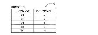
- the BOM data is a table in which items such as “reference” and “part number” are set as one set.
- the “part number” is an identifier for specifying an electronic component to be mounted, and is information including, for example, a manufacturer and a product number of the electronic component.
- the part data 43 includes “part number” “lead 1 (X coordinate)” “lead 1 (Y coordinate)” “lead 2 (X coordinate)” “lead 2 (Y coordinate)” “lead”.
- the table includes a set of items such as “length”, “part height”, “bending position”, “remaining lead length”, and “supply type”.
- FIG. 4 illustrates a lead component having a pair of leads.
- lead 1 (X coordinate) and lead 1 (Y coordinate) are relative coordinates with respect to the reference position of the lead component of one lead
- lead 2 (X coordinate) and lead 2 (Y coordinate) is a relative coordinate with respect to the reference position of the lead component of the other lead.
- “Supply type” includes, for example, “radial” in the case of radial equipment, “axial” in the case of axial parts, and the like. Note that the items of the part data 43 are appropriately changed according to the type of electronic component.
- FIG. 5 is a cross-sectional view showing the substrate board cut along a plane passing through two holes hole formed in the substrate board.
- a capacitor C1 is shown as an example of a lead component having a main body and leads.
- the capacitor C1 has a body body and a pair of leads lead attached to the body body.
- FIG. 5 shows a state in which the pair of leads lead of the capacitor C1 is inserted into the pair of holes hole and the leads lead are bent.
- one surface of the substrate which is the surface on which the main body of the lead component is disposed, is referred to as the front surface, and the other surface is referred to as the back surface.
- [Lead length] is the total length of the lead lead indicated by “l” in FIG.
- Part height is a clearance from the surface of the board “board” to the main body “b” indicated by “h” in FIG.
- the “folding position” is a clearance from the back surface of the substrate board to the lead lead lead, which is indicated by “p” in FIG.
- the “lead remaining length” is a length from the bending position to the tip of the lead lead, which is indicated by “rl” in FIG.
- t is the thickness of the substrate board.
- the substrate thickness value is included in the CAD data 31.
- the Gerber data 32 will be described with reference to FIG.
- FIG. 6 is a schematic diagram of wirings and lands formed on the substrate.
- the hatched portion in FIG. 6 is a metal pattern such as a copper foil.
- An annular pattern is a land surrounding the hole.
- the wiring extends from the land.
- the gerber data 32 is data conforming to the gerber format, and is data including information such as a metal pattern and a shape / position of a hole in which a through hole is formed. For example, an image as shown in FIG. 6 can be displayed on, for example, a display by drawing based on the Gerber data 32.
- the data creation device 10 has an automatic generation mode and a manual generation mode.
- the data creation device 10 automatically determines the lead bending direction in the automatic generation mode.
- the data creation device 10 displays an image for the operator to determine the lead bending direction on the display 15 and determines the lead bending direction based on the operator's instruction.
- the automatic generation mode will be described with reference to FIGS.
- the operator who wants to execute the automatic generation mode operates the data creation device 10 and activates an application for performing the first data creation processing and the second data creation processing, which is installed in the data creation device 10 in advance.
- CPU11 will start a 1st data creation process, if the operation start in automatic generation mode is instruct
- the CPU 11 imports various data (S1).
- the various data includes CAD data 31, Gerber data 32, BOM data 33, part data included in the part data database 21, and the like.
- the CPU 11 converts the received CAD data 31, gerber data 32, and BOM data 33 via the communication unit 17, for example, and stores them in the RAM 12 as necessary.
- the imported Gerber data 32 is a part of the verify data 42.
- the substrate data 34 is extracted from the CAD data 31.
- the CPU 11 requests the server 20 to transmit part data of each value of the part number included in the BOM data 33.
- the part data transmitted from the server 20 in response to the request is subjected to format conversion as necessary, and then stored as part data 43 in the RAM 12.
- the CPU 11 creates sequence data 41.
- the sequence data 41 is a table in which items such as “reference”, “part number”, “X coordinate”, “Y coordinate”, “ ⁇ axis coordinate”, and “lead bending” are set.
- “X coordinate” and “Y coordinate” are relative coordinates of the reference position of the electronic component with respect to the reference position of the board mounting machine.
- “Theta axis coordinate” is an angle of the reference axis of the electronic component with respect to the reference axis defined by “X coordinate” and “Y coordinate” in the horizontal direction.
- the reference axis is, for example, the positive direction of the X axis. Note that the XY directions in the coordinates conform to the directions defined by the board mounting machine.
- the CPU 11 determines values of “reference” and “part number” based on the board data 34 and the BOM data 33.
- the CPU 11 determines the values of “X coordinate”, “Y coordinate”, and “ ⁇ axis coordinate” based on the substrate data 34.
- the value of “lead bending” in the sequence data is blank.
- the CPU 11 determines a value of “cut length” which is an item of sequence data 41 (not shown). Based on the part data 43, if the value obtained by subtracting each value of the component height, the substrate thickness, the bending position, and the remaining lead length from the lead length value is 0 or more, the CPU 11 sets the value as “cut length”. ".
- the mounting order of the electronic components on the board is determined based on the various data, and the mounting order data 44 is created (S3).
- the value of “lead bending” is determined in order from the lead component in the top row of the sequence data 41.
- the value of “lead bending” is any one of “inner bending”, “outer bending”, and “N bending”.
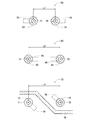
- FIG. 9 is a schematic view of the back surface of the substrate on which the metal pattern is formed. Patterns 50, 60, and 70 indicate metal patterns when determined as outer bending, inner bending, and N bending, respectively.
- FIG. 9 shows leads 55, 56, 65, 66, 75, and 76 that are cut and bent along with the patterns 50, 60, and 70.
- the distance between the centers of a pair of holes whose centers are the centers 51 and 52 is the distance L1.
- the lands 53 and 54 are formed surrounding the two holes.
- the distance between the centers of a pair of holes whose centers are the centers 61 and 62 is the distance L2. Surrounding two holes, there are lands 63, 64.
- the distance between the centers of a pair of holes whose centers are the centers 71 and 72 is a distance L2.
- the distance L1 is shorter than the distance L2.
- the CPU 11 determines “lead bending” as “outside bending”. As indicated by the pattern 50, the outward bending is bending in the direction in which the pair of leads are separated from each other along the direction in which the pair of leads of the lead component are arranged. When the distance between the holes is longer than the reference value and there is no metal pattern between the pair of holes, the CPU 11 determines “lead bending” as “inner bending”. As indicated by the pattern 60, the internal bending is bending in a direction in which the pair of leads approach each other along the direction in which the pair of leads of the lead component are arranged.
- the CPU 11 determines “lead bending” as “N bending”. As indicated by the pattern 70, the N-bending is a bending in a direction different from the direction in which the pair of leads of the lead component are arranged. If the distance between the holes is short with respect to the remaining lead length of the lead, if the leads are bent inward, a pair of leads may come into contact with each other. Therefore, when the distance between the holes is shorter than the remaining lead length, the CPU 11 determines that the lead is bent outward.
- the CPU 11 determines that the leads are bent inward.
- the CPU 11 determines the lead to be N-bent.
- step S4 the CPU 11 determines whether or not the determination of the lead bending direction is completed (S4).
- the CPU 11 determines that the determination of the lead bending direction is not completed when there is a row in which the value of “lead bending” in the sequence data is blank. If it is determined that the determination of the lead bending direction has been completed (S4: YES), the process is terminated. On the other hand, if it is determined that the determination of the lead bending direction has not been completed (S4: NO), the distance between the holes of the lead component is determined for a reference in which the value of “lead bending” is blank in order to determine the lead bending direction.
- the reference value is a value obtained by adding a margin value to twice the remaining lead length of the target reference. If it is determined that the distance between holes is not larger than the reference value (S5: NO), the value of “lead bending” is determined to be “outside bending”. On the other hand, if it is determined that the distance between holes is larger than the reference value (S5: YES), it is determined whether or not there is a metal pattern between a pair of holes of the target reference (S9). If it is determined that there is no metal pattern between the pair of holes (S9: NO), the value of “lead bending” is determined to be “inner bending”. On the other hand, if it is determined that there is a metal pattern between the pair of holes (S9: YES), the value of “lead bending” is determined to be “N bending”.
- Step S7 After executing Steps S7, S11, and S13, the process returns to Step S4, and the process is continued until it is determined that the determination of the lead bending direction is completed (S4: YES).
- the CPU 11 can acquire the reference coordinates and the arrangement direction of the target reference on the board by referring to the target row of the board data 34. Further, by referring to the part data 43 of the reference part number of the target, the coordinates of each lead on the target reference substrate can be acquired. As a result, the CPU 11 can acquire the coordinates on the substrate of each lead of the target reference.
- the CPU 11 specifies a hole or land pattern corresponding to each lead in the Gerber data included in the verify data 42 based on the coordinates of each lead on the substrate. Thereby, the CPU 11 can acquire the distance of the target reference hole. It is also possible to determine whether or not there is a metal pattern between target reference holes.
- the CPU 11 starts the second data creation process.
- the CPU 11 executes the same steps as steps S1 and S3 of the first data creation process.
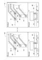
- the display screen shown in FIG. 10 is displayed on the display 15 based on various data.
- the data creation device 10 includes a display screen of the first display mode 80 that is a display mode for displaying a state when the lead bending direction is external bending, and the lead bending direction is internal bending.
- the display screen of the second display mode 81 which is a display mode for displaying the state in the case of having been displayed is displayed on the display 15.
- the CPU 11 displays a switching button (not shown) on the display 15 and switches the first display mode 80 and the second display mode 81 to toggle according to the operation of the switching button by the operator.
- the first display mode 80 has a first display window window1 and a second display window window2.
- the back surface of the substrate 89 is displayed in the first display window window1, and the cross section of the substrate 89 is displayed in the second display window window2.
- a metal pattern based on Gerber data for example, an external shape of an electronic component based on part data 43 and an external shape of a lead that is bent outward are displayed.
- capacitors C1 and C2 which are lead parts are illustrated as electronic parts.
- the metal pattern is shown by hatching in FIG. 10, and specifically, a land and a wiring pattern 87 surrounding the holes 83 and 84 into which the leads of the capacitor C1 are inserted.
- the leads 85 and 86 are releads attached to the capacitor C1.
- the second display window window 2 is a cross-sectional view with a center line 82 passing through the centers of the holes 83 and 84 indicated by the first display window window 1 as a cut surface.
- the upper side is the surface of the substrate 89, and the lower side is the back surface of the substrate.
- holes 83 and 84, leads 85 and 86 bent outward, and a wiring pattern 87 are shown.
- the second display mode 81 has a first display window window1 and a second display window window2.
- the leads 85 and 86 are displayed in a state where they are inserted into the holes 83 and 84 and bent inward.
- the operator can confirm the lead bending direction by viewing the display screens of the first display mode 80 and the second display mode 81.
- On the display screen of the first display mode 80 a state in which the outwardly bent lead 86 and the wiring pattern 87 are approaching each other is displayed.
- the bending direction can be determined by looking at the display screen, such as setting the bending direction to inward bending.
- the data creation device 10 displays the display screen of the first display mode 80 or the display screen of the second display mode 81 on the display 15 and receives, for example, the value of “lead bending” of the sequence data 41. For example, an “inner bend” button and an “outer bend” button that can be selected are displayed.
- the CPU 11 sets one of the received “inner bend” and “outer bend” as the value of “lead bend” in the sequence data 41.
- the job data 40 is an example of NC data used in the cut and clinching device
- the data creation device 10 is an example of a data creation device.
- the CAD data 31 and the Gerber data 32 are examples of wiring pattern information
- the CPU 11 that executes the first data creation process and the second data creation process is an example of a determination unit.
- Inner bending is an example of the first bending direction
- outer bending is an example of the second bending direction
- N bending is an example of the third bending direction.
- Step S9 is an example of a first determination process
- step S13 is an example of a first determination process.
- Step S5 is an example of an acquisition process and a second determination process
- step S7 is an example of a second determination process.
- the reference is an example of an identifier of a lead component in the circuit diagram, and the metal pattern is an example of a wiring pattern.
- the display 15 is an example of a display unit, and the operation unit 16 is an example of a reception unit.
- the process in which the CPU 11 displays the display screen of the first display mode 80 on the display 15 is an example of the first display process
- the process in which the CPU 11 displays the display screen of the second display mode 81 on the display 15 is the second process. It is an example of a display process.
- the CPU 11 determines the value of the “lead bending” item of the sequence data 41 included in the job data 40 based on the CAD data 31 and the Gerber data 32. Thereby, the data creation device 10 can create job data 40 in which the lead bending direction of the lead component is the optimum direction.
- the CPU 11 sets the value of the “lead bending” item of the sequence data 41 to any one of inner bending, outer bending, and N bending based on the CAD data 31, the Gerber data 32, and the BOM data. decide.
- the data creation device 10 can create job data 40 that can avoid contact between the metal pattern and the bent lead, which may occur when the bending direction is inward bending. If it is determined that the distance between the leads is not larger than the reference value (S5: NO), the value of “lead bending” is determined as outer bending. Thereby, the data creation device 10 can create job data 40 that can avoid contact between a pair of bent leads that may occur when the bending direction is inward bending.
- the CPU 11 displays the display screen of the first display mode 80 on the display 15. Further, the display screen of the second display mode 81 is displayed on the display 15. Thereby, the operator can see the display screen of the bent lead along with the metal pattern of the substrate. The operator can select the optimal bending direction by looking at the display screen.
- the data creation device 10 can determine the accepted outer bend or inner bend as the “lead bend” value in the sequence data 41.
- the present invention is not limited to the above-described embodiment, and various improvements and modifications can be made without departing from the spirit of the present invention.
- the value of “lead bending” is determined to be “N bending”.
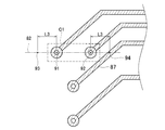
- the value of “lead bending” is set to “N bending”. May be determined. This will be described in detail with reference to FIG.
- a rectangle indicated by a broken line is an outer shape of a capacitor C1 which is an example of a lead component.
- the center line 82 is a line passing through the centers 91 and 92 that are the centers of the pair of holes into which the pair of leads of the capacitor C1 are inserted.
- a point 93 is a point on the center line 82 that is away from the center 91 by a distance L3 in a direction opposite to the direction from the center 91 to the center 92.
- the point 94 is a point on the center line 82 that is away from the center 92 by a distance L3 in a direction opposite to the direction from the center 92 to the center 91.
- the CPU of the data creation device determines whether there is a metal pattern isolated from the land in the region from the center 91 to the point 93 and the region from the center 92 to the point 94 (an example of third determination processing). ).
- the distance L3 is a value equivalent to the “read remaining length” of the part data 43. If it is determined that there is a metal pattern isolated from the land, the value of “lead bending” is determined to be “N bending” (an example of third determination processing). In the example of FIG. 6, there is no metal pattern isolated from the land in the region from the center 91 to the point 93, but there is a wiring pattern 87 which is a metal pattern isolated from the land in the region from the center 92 to the point 94.
- N-bending prevents contact between the lead and the wiring pattern 87. According to this configuration, it is possible to create job data 40 that can avoid contact between a bent lead and a metal pattern, which may occur when “lead bending” is set to “outside bending”.
- the data creation device 10 has been described as executing either the first data creation process or the second data creation process.
- the present invention is not limited to this.
- a configuration may be adopted in which the “lead bending” value is automatically determined or manually determined.
- a part of the values may be updated.
- the association between the reference and the part number defined by the BOM data 33 may be changed.
- the part number of the BOM data 33 may be updated by reading a barcode associated with the electronic component. In this case, it is preferable to execute the first data creation process for the corresponding reference as a trigger when the barcode is read.
- the procedure of the first data creation process is not limited to the above.
- the bending direction is directed from the hole to the direction in which the metal pattern is present. It may be other than the direction.
- the metal pattern isolated from the land for example, the chip component that is surface-mounted on the back side of the substrate, the presence or absence of the lead of a lead component different from the target lead component, etc. It is good also as conditions to determine.
- the display screen displayed in the second data creation process is not limited to the above.
- it is good also as a structure which displays any one of the 1st display window window1 and the 2nd display window window2.
- sequence data 41 has the item “part number”, it may be configured not to have the item “part number”. In this case, it is preferable to refer to the imported BOM data 33.
- the lead component having two leads has been described.
- the above configuration can be applied to a lead component having three or more leads.
- the first judgment process to the third judgment process are executed for two adjacent leads among the three or more leads, and the first judgment is performed for all the leads. It is preferable that the determination process to the third determination process be executed.
- Data Creation System 10 Data Creation Device 11 CPU 31 CAD data 32 Gerber data 33 BOM data 40 Job data 41 Sequence data 43 Part data 100 Cut and clinching device
Landscapes
- Engineering & Computer Science (AREA)
- Manufacturing & Machinery (AREA)
- Microelectronics & Electronic Packaging (AREA)
- Electric Connection Of Electric Components To Printed Circuits (AREA)
- Structures For Mounting Electric Components On Printed Circuit Boards (AREA)
- Supply And Installment Of Electrical Components (AREA)
Abstract
リード部品のリードの曲げ方向を最適な方向とするデータ作成装置を提供することを課題とする。CPU11はホール間に金属パターンがあると判断すると(S9:YES)、「リード折り曲げ」の値をN曲げに決定する。これにより、データ作成装置10は、屈曲方向を内曲げとした場合に生じるおそれのある、金属パターンと屈曲されたリードとの接触を回避することができるジョブデータ40を作成することができる。
Description
本発明は、リード部品の基板挿入に係わるデータ作成装置およびデータ作成プログラムに関するものである。
従来より、CADシステムなどにおいて、基板における部品配置の設計を支援する技術がある。例えば、特許文献1には、リード部品(挿入型部品)を基板に挿入する挿入工程などを考慮して、電子部品の配置の禁止領域を明示することにより、設定を支援する技術が記載されている。
特許文献1では、リード線が、リード部品の2つのランドの並ぶ方向に沿って、リード部品の内側に曲げられる例が記載されている。これに限らず、近年、リード部品のリードを上記とは異なる方向へ曲げることができる実装装置も提案されている。
さて、基板へのリード部品の挿入、続く、リード線の切断、屈曲を行う実装装置は、一般にNCデータに基づいて動作する。NCデータは、基板におけるリード部品などの電子部品の配置位置、電子部品の部品名などを含む設計情報に基づき、作成される。
しかしながら、NCデータの作成の際に、上記のリード線の曲げ方向に関する設計情報が供給されない場合もある。この場合、リードの曲げ方向を最適な向きとして、NCデータを作成する必要がある。
本発明は、上記の課題に鑑みてなされたものであり、リード部品のリードの曲げ方向を最適な方向とするデータ作成装置を提供することを目的とする。
(1)本願に係るデータ作成装置は、基板に設けられたホールにリードが挿入されることによって基板に装着されたリード部品の、当該リードの切断および屈曲を行うカットアンドクリンチ装置で使用するNCデータを作成するデータ作成装置であって、基板の配線パターン情報に基づいて、リード部品のリードの屈曲方向を決定する決定手段を備えることを特徴とする。このようにすると、データ作成装置はリード部品のリードの曲げ方向を最適な方向とすることができる。
(2)また、決定手段は、屈曲方向を、リード部品の1対のリードの並ぶ第1方向であって、当該1対のリードが接近する第1屈曲方向、第1方向であって、当該1対のリードが離間する第2屈曲方向、あるいは、第1方向とは異なる第2方向であって、当該1対のリードが離間する第3屈曲方向、の何れかとすることを特徴とする。このようにすると、データ作成装置は屈曲方向を第1屈曲方向、第2屈曲方向、第3屈曲方向の何れかとすることができる。
(3)また、決定手段は、第1方向において、1対のリードが挿入される1対のホール間に、ホールを囲むランドから隔離された配線パターンがあるか否かを判断する第1判断処理と、ランドから隔離された配線パターンがあると判断した場合、屈曲方向を、第2屈曲方向、もしくは、第3屈曲方向とする第1決定処理とを実行することを特徴とする。このようにすると、データ作成装置は、屈曲方向を第1屈曲方向とした場合に生じるおそれのある、配線パターンと屈曲されたリードとの接触を回避することができるデータを作成することができる。
(4)また、決定手段は、1対のホール間距離を取得する取得処理と、1対のホール間距離が、第1屈曲方向に屈曲させた1対のリードが非接触を維持するのに必要な所定の最小距離より短いか否かを判断する第2判断処理と、最小距離より短いと判断した場合、屈曲方向を、第2屈曲方向、もしくは、第3屈曲方向とする第2決定処理とを実行することを特徴とする。このようにすると、データ作成装置は、屈曲方向を第1屈曲方向とした場合に生じるおそれのある、屈曲された1対のリード同士の接触を回避することができるデータを作成することができる。
(5)決定手段は、1対のリードが挿入される1対のホールの各々について、第1方向であって、1対のホールの一方から1対のホールの他方と離間する方向に向かう方向において、1対のホールの一方を基点とし、基点から所定距離までの領域に、ホールを囲むランドから隔離された配線パターンがあるか否かを判断する第3判断処理と、ランドから隔離された配線パターンがあると判断した場合、屈曲方向を、第3屈曲方向とする第3決定処理とを実行することを特徴とする。このようにすると、データ作成装置は、屈曲方向を第2屈曲方向とした場合に生じるおそれのある、屈曲されたリードと配線パターンとの接触を回避することができるデータを作成することができる。
(6)決定手段は、回路図におけるリード部品の識別子と、配線パターン情報により特定されるリード部品の基板における配置位置および配置方向とが関連づけられたCADデータと、識別子と、リード部品を特定する部品名とが対応づけられたBOMデータと、リード部品の基準座標と、基準座標に対する1対のリードの相対座標とが含まれるパートデータと、に基づき、識別子毎に、識別子に対応付けられた部品名における基準座標を配置位置に対応させ、配置方向と相対座標に応じて、ホールの位置と屈曲方法を決定することを特徴とする。このようにすると、データ作成装置は、CADデータ、BOMデータ、およびパートデータに基づき、データを作成することができる。
(7)基板に設けられたホールにリードが挿入されることによって基板に装着されたリード部品の、当該リードの切断および屈曲を行うカットアンドクリンチ装置で使用するNCデータを作成するデータ作成装置であって、基板の配線パターン情報を表示する表示手段と、受付手段と、屈曲方向を決定する決定手段と、を備え、決定手段は、リード部品の1対のリードの並ぶ第1方向であって、当該1対のリードが接近する第1屈曲方向に屈曲された状態のリードを配線パターンとともに表示手段に表示させる第1表示処理、および、第1方向であって、当該1対のリードが離間する第2屈曲方向に屈曲された状態のリードを配線パターンとともに表示手段に表示させる第2表示処理、の少なくとも何れか一方を実行し、受付手段にて屈曲方向として受け付けた第1屈曲方向もしくは第2屈曲方向を、データにおける屈曲方向に決定することを特徴とする。このようにすると、データ作成装置は、配線パターンとともに、屈曲された状態のリードを配線パターンとともに表示手段に表示させることができる。オペレータは、表示を見て、最適な屈曲方向を選択することができる。データ作成装置は、受け付けた第1屈曲方向もしくは第2屈曲方向をデータにおける屈曲方向に決定することができる。
さらに、本願に係る発明は、データ作成装置の発明に限定されることなく、データ作成装置を制御するプログラムの発明としても実施し得るものである。
本願に係るデータ作成装置などによれば、リード部品のリードの曲げ方向を最適な方向とするデータ作成装置を提供することができる。
[第1実施形態]
<データ作成システムの構成>
図1を用いて、データ作成システム1の構成について説明する。データ作成システム1はデータ作成装置10およびサーバ20を備える。データ作成装置10は、例えばPCで実現され、CPU11、RAM12、ROM13、NVRAM(不揮発性RAM)14、ディスプレイ15、操作部16、通信部17などを有する。CPU11はROM13に記憶されている各種のプログラムを実行することによって、接続されているディスプレイ15などを制御する。RAM12はCPU11が各種の処理を実行するための主記憶装置として用いられる。ROM13には第1データ作成処理(後述)および第2データ作成処理(後述)のプログラム、制御プログラム、および各種のデータなどが記憶されている。NVRAM14には各種情報が記録されている。ディスプレイ15は、例えば液晶ディスプレイであり、CPU11の命令に従って、例えば各種の設定画面や装置の動作状態などを表示する。操作部16は不図示のキーボードおよびマウスを有し、オペレータの操作を受け付ける。通信部17はネットワークを介して、サーバ20とデータの送受を行う。サーバ20は、パートデータデータベース21を有しており、クライアントであるデータ作成装置10からの要求に応じて、パートデータデータベース21が有するパートデータを提供する。
<データ作成システムの構成>
図1を用いて、データ作成システム1の構成について説明する。データ作成システム1はデータ作成装置10およびサーバ20を備える。データ作成装置10は、例えばPCで実現され、CPU11、RAM12、ROM13、NVRAM(不揮発性RAM)14、ディスプレイ15、操作部16、通信部17などを有する。CPU11はROM13に記憶されている各種のプログラムを実行することによって、接続されているディスプレイ15などを制御する。RAM12はCPU11が各種の処理を実行するための主記憶装置として用いられる。ROM13には第1データ作成処理(後述)および第2データ作成処理(後述)のプログラム、制御プログラム、および各種のデータなどが記憶されている。NVRAM14には各種情報が記録されている。ディスプレイ15は、例えば液晶ディスプレイであり、CPU11の命令に従って、例えば各種の設定画面や装置の動作状態などを表示する。操作部16は不図示のキーボードおよびマウスを有し、オペレータの操作を受け付ける。通信部17はネットワークを介して、サーバ20とデータの送受を行う。サーバ20は、パートデータデータベース21を有しており、クライアントであるデータ作成装置10からの要求に応じて、パートデータデータベース21が有するパートデータを提供する。
データ作成装置10は、CADデータ31、ガーバデータ32、BOMデータ33、およびパートデータデータベース21が有するパートデータなどに基づき、NCデータであるジョブデータ40を作成する。作成されたジョブデータ40はカットアンドクリンチ装置100などを制御する制御装置へ提供される。ジョブデータ40は、シーケンスデータ41、ベリファイデータ42、パートデータ43、装着順データ44などを含む。
<カットアンドクリンチ装置の構成>
カットアンドクリンチ装置100は、例えばプリント基板なのどの基板に挿入されたリード部品のリードの屈曲および切断を行う装置である。カットアンドクリンチ装置100は、不図示のユニット移動装置およびカットアンドクリンチユニットを備える。ユニット移動装置は、カットアンドクリンチユニットのX方向、Y方向、Z方向(後述)への移動などを行う。カットアンドクリンチユニットは、1対のリードが挿入される1対の挿入穴を備えている。カットアンドクリンチ装置100は、1対の挿入穴に挿入された1対のリードを所定の方向に屈曲させる機能、およびリードを所定の長さで切断する機能を有している。
カットアンドクリンチ装置100は、例えばプリント基板なのどの基板に挿入されたリード部品のリードの屈曲および切断を行う装置である。カットアンドクリンチ装置100は、不図示のユニット移動装置およびカットアンドクリンチユニットを備える。ユニット移動装置は、カットアンドクリンチユニットのX方向、Y方向、Z方向(後述)への移動などを行う。カットアンドクリンチユニットは、1対のリードが挿入される1対の挿入穴を備えている。カットアンドクリンチ装置100は、1対の挿入穴に挿入された1対のリードを所定の方向に屈曲させる機能、およびリードを所定の長さで切断する機能を有している。
<基板実装機の構成>
また、カットアンドクリンチ装置100は、不図示の基板実装機に備えられている。基板実装機はカットアンドクリンチ装置100の他に、不図示の装置本体、基板搬送保持装置、部品装着装置、部品供給装置、カメラ、制御装置などを備え、基板に電子部品を実装する。カットアンドクリンチ装置100、基板搬送保持装置、部品装着装置、および部品供給装置などは基板実装機の装置本体に配設されている。
また、カットアンドクリンチ装置100は、不図示の基板実装機に備えられている。基板実装機はカットアンドクリンチ装置100の他に、不図示の装置本体、基板搬送保持装置、部品装着装置、部品供給装置、カメラ、制御装置などを備え、基板に電子部品を実装する。カットアンドクリンチ装置100、基板搬送保持装置、部品装着装置、および部品供給装置などは基板実装機の装置本体に配設されている。
基板搬送保持装置は、基板を搬送し、所定の位置にて基板を保持する。以下の説明において、基板の搬送方向をX方向、X方向と直交する水平方向をY方向、鉛直方向をZ方向と称する。部品装着装置は吸着ノズルを備え、部品供給装置により供給される電子部品を吸着ノズルで吸着して保持する。電子部品がリード部品である場合、部品装着装置は、保持したリード部品の1対のリードを基板に形成された1対の例えばスルーホールなどのホールに挿入して、装着する。カットアンドクリンチ装置100は、所定の位置に保持されている基板の下方に配設されている。リード部品の基板への挿入時、1対のホールの下にカットアンドクリンチユニットの1対の挿入穴が位置するように、カットアンドクリンチユニットは移動する。次に、カットアンドクリンチユニットが、リードが挿入されている1対の挿入穴を操作することにより、1対のリードの屈曲および切断がなされる。これにより、リード部品の基板からの抜けが防止される。
ベリファイデータ42は、基板実装機が設定通りに作業を行うために用いるデータである。例えば、ベリファイデータ42には、基板の金属パターンおよびホールなどの位置・形状のデータが含まれている。部品装着装置がリード部品を基板に装着する際には、基板をカメラで撮像し、得られた画像と、ベリファイデータ42に含まれる基板に関するデータとが照合される。これにより、部品装着装置は設定された位置にリード部品を装着することができる。
尚、基板実装機が備える各装置は、基板実装機が備える制御装置により制御される。ジョブデータ40は制御装置に提供され、これにより、カットアンドクリンチ装置100はジョブデータ40に基づいて制御される。
<各種データの構成>
次に、図2~6を用いて各種データについて説明する。尚、以下の説明では、適宜、電子部品としてリード部品を例示して説明する。CADデータ31は基板における電子部品、例えばプリント配線などの配線、ホールなどの形状・位置などの情報を含む。データ作成装置10は、CADデータ31から図2に示す基板データ34を抽出することができる。基板データ34は「リファレンス」「基準座標(X座標)」「基準座標(Y座標)」「配置方向」などの項目が1組とされたテーブルである。リファレンスとは、基板に実装される電子部品の各々に一意に付与される識別子である。リファレンスは、回路図にて電子部品の各々に一意に付与される名称が引用される。基準座標とは、基板の基準位置に対する、パートデータデータベース21が有するパートデータにおいて規定される電子部品の基準位置の相対座標である。配置方向とは、基板の基準方向に対する、電子部品の配置方向であり、パートデータデータベース21が有するパートデータにおいて規定される電子部品の基準方向に基づく方向である。ここでは、基板の基準方向は、矩形である基板の長辺方向がX方向、短辺方向がY方向とされ、リード部品の基準方向は、リードが並ぶ方向がX方向、X方向と直交する方向がY方向とされているものとする。この場合、リード部品のX方向が、基板のX方向と揃えられて、配置される場合は「横」、リード部品のY方向が、基板のX方向と揃えられて、配置される場合は「縦」とされる。
次に、図2~6を用いて各種データについて説明する。尚、以下の説明では、適宜、電子部品としてリード部品を例示して説明する。CADデータ31は基板における電子部品、例えばプリント配線などの配線、ホールなどの形状・位置などの情報を含む。データ作成装置10は、CADデータ31から図2に示す基板データ34を抽出することができる。基板データ34は「リファレンス」「基準座標(X座標)」「基準座標(Y座標)」「配置方向」などの項目が1組とされたテーブルである。リファレンスとは、基板に実装される電子部品の各々に一意に付与される識別子である。リファレンスは、回路図にて電子部品の各々に一意に付与される名称が引用される。基準座標とは、基板の基準位置に対する、パートデータデータベース21が有するパートデータにおいて規定される電子部品の基準位置の相対座標である。配置方向とは、基板の基準方向に対する、電子部品の配置方向であり、パートデータデータベース21が有するパートデータにおいて規定される電子部品の基準方向に基づく方向である。ここでは、基板の基準方向は、矩形である基板の長辺方向がX方向、短辺方向がY方向とされ、リード部品の基準方向は、リードが並ぶ方向がX方向、X方向と直交する方向がY方向とされているものとする。この場合、リード部品のX方向が、基板のX方向と揃えられて、配置される場合は「横」、リード部品のY方向が、基板のX方向と揃えられて、配置される場合は「縦」とされる。
BOMデータは、図3に示すように、「リファレンス」「パートナンバー」などの項目が1組とされたテーブルである。「パートナンバー」とは、実装される電子部品を特定する識別子であり、例えば電子部品の製造元および品番などを含む情報である。
パートデータ43は、図4に示すように、「パートナンバー」「リード1(X座標)」「リード1(Y座標)」「リード2(X座標)」「リード2(Y座標)」「リード長」「部品高さ」「折り曲げ位置」「リード残長」「供給形式」などの項目が1組とされたテーブルである。尚、図4は1対のリードを有するリード部品について例示している。例えば、2つのリードを有するリード部品の場合、リード1(X座標)およびリード1(Y座標)は一方のリードのリード部品の基準位置に対する相対座標であり、リード2(X座標)およびリード2(Y座標)は他方のリードのリード部品の基準位置に対する相対座標である。「供給形式」には、例えばラジアル備品の場合の「ラジアル」、アキシャル部品の場合の「アキシャル」などがある。尚、パートデータ43は、電子部品の種類に応じて、項目が適宜変更される。
「リード長」「部品高さ」「折り曲げ位置」「リード残長」については、図5を用いて説明する。図5は、基板boardを、基板boardに形成された2つのホールholeを通る面で切断して示す断面図である。ここでは、本体およびリードを有するリード部品の一例としてコンデンサC1を示す。コンデンサC1は本体bodyと、本体bodyに取り付けられた1対のリードleadを有する。尚、図5では、コンデンサC1の1対のリードleadが1対のホールholeに挿入され、リードleadが屈曲されている状態を示している。以下の説明において、リード部品の本体が配置される側の面である、基板の一方の面を表面、他方の面を裏面と称する。[リード長]は図5において「l」で示す、リードleadの全長である。「部品高さ」は、図5において「h」で示す、基板boardの表面から本体bodyまでのクリアランスである。「折り曲げ位置」は、図5において「p」で示す、基板boardの裏面からリードleadまでのクリアランスである。「リード残長」とは、図5において「rl」で示す、折り曲げ位置からリードleadの先端までの長さである。
尚、図5において「t」は、基板boardの厚さである。基板の厚さの値は、CADデータ31に含まれている。
ガーバデータ32について図6を用いて説明する。図6は、基板に形成された配線およびランドの模式図である。図6の斜線部は、例えば銅箔などの金属パターンである。円環状のパターンはホールを取り囲むランドである。ランドから配線が延伸している。ガーバデータ32は、ガーバフォーマットに則ったデータであり、金属パターン、スルーホールが形成されるホールの形状・位置などの情報を含むデータである。例えば、ガーバデータ32に基づく描画により、図6に示すような画像を例えばディスプレイなどに表示させることができる。
<データ作成処理>
データ作成装置10は、自動生成モードおよび手動生成モードを有する。データ作成装置10は、自動生成モードにおいて、自動でリードの折り曲げ方向を決定する。データ作成装置10は、手動生成モードにおいて、ディスプレイ15にオペレータがリードの折り曲げ方向を決定するための画像を表示し、オペレータの指示に基づき、リードの折り曲げ方向を決定する。まず、自動生成モードについて図7~9を用いて説明する。
データ作成装置10は、自動生成モードおよび手動生成モードを有する。データ作成装置10は、自動生成モードにおいて、自動でリードの折り曲げ方向を決定する。データ作成装置10は、手動生成モードにおいて、ディスプレイ15にオペレータがリードの折り曲げ方向を決定するための画像を表示し、オペレータの指示に基づき、リードの折り曲げ方向を決定する。まず、自動生成モードについて図7~9を用いて説明する。
自動生成モードを実行させたいオペレータは、データ作成装置10を操作し、予めデータ作成装置10にインストールされている、第1データ作成処理および第2データ作成処理を行うアプリケーションを起動する。CPU11は、オペレータにより、自動生成モードでの動作開始が指示されると、第1データ作成処理を開始する。まず、CPU11は、各種データをインポートする(S1)。ここで、各種データとは、CADデータ31、ガーバデータ32、BOMデータ33、パートデータデータベース21が有するパートデータなどである。詳しくは、CPU11は、例えば通信部17を介して、受信したCADデータ31、ガーバデータ32、BOMデータ33を、必要に応じて形式変換して、RAM12に記憶させる。インポートしたガーバデータ32は、ベリファイデータ42の一部とされる。また、CADデータ31から基板データ34を抽出する。CPU11は、必要なパートデータを取得するため、BOMデータ33に含まれるパートナンバーの各値のパートデータの送信を、サーバ20へ要求する。要求に応じてサーバ20から送信されるパートデータを、必要に応じて形式変換した後、パートデータ43として、RAM12に記憶する。
次に、CPU11はシーケンスデータ41を作成する。シーケンスデータ41は、図8に示すように、「リファレンス」「パートナンバー」「X座標」「Y座標」「θ軸座標」「リード折り曲げ」などの項目が1組とされたテーブルである。「X座標」「Y座標」は、基板実装機の基準位置に対する電子部品の基準位置の相対座標である。「シータ軸座標」は、水平方向における、「X座標」「Y座標」で規定される基準軸に対する電子部品の基準軸の角度である。基準軸は例えばX軸の正方向などとされる。尚、座標におけるXY方向は、基板実装機で規定されている方向に準じている。CPU11は基板データ34およびBOMデータ33に基づき、「リファレンス」「パートナンバー」の値を決定する。CPU11は基板データ34に基づき、「X座標」「Y座標」「θ軸座標」の値を決定する。尚、この段階では、「リード折り曲げ」は決定していないため、シーケンスデータの「リード折り曲げ」の値は空欄とされている。
また、CPU11は不図示のシーケンスデータ41の項目である「カット長」の値を決定する。パートデータ43に基づき、CPU11はリード長の値から、部品高さ、基板厚さ、折り曲げ位置、およびリード残長の各値を減じた値が0以上であった場合、当該値を「カット長」の値とする。
次に、各種データに基づき、電子部品の基板への装着順序を決定し、装着順データ44を作成する(S3)。次に、例えば、シーケンスデータ41の最上段の行にあるリード部品から順に、「リード折り曲げ」の値を決定する。尚、「リード折り曲げ」の値は、「内曲げ」「外曲げ」「N曲げ」の何れかとされる。
ここで、「リード折り曲げ」の値の決定方法について、図9を用いて説明する。カットアンドクリンチ装置100は、内曲げ、外曲げ、N曲げの3つの状態にリードを屈曲させることができる。図9は金属パターンが形成されている基板の裏面の模式図である。パターン50,60,70は、夫々、外曲げ、内曲げ、N曲げと決定される場合の金属パターンを示している。また、図9では、パターン50,60,70とともに、切断および屈曲された状態のリードであるリード55,56,65,66,75,76を示している。パターン50は、中心を中心51,52とする1対のホールの中心間距離は距離L1である。2つのホールを取り囲み、ランド53,54が形成されている。パターン60は、中心を中心61,62とする1組のホールの中心間距離は距離L2である。2つのホールを取り囲み、ランド63,64がある。パターン70は、中心を中心71,72とする1組のホールの中心間距離は距離L2である。2つのホールを取り囲み、ランド73,74がある。ランド73,74の間に、配線パターン78がある。ここで、距離L1は距離L2よりも短い。
CPU11は、1対のホールのホール間距離が基準値より短い場合には、「リード折り曲げ」を「外曲げ」と決定する。パターン50にて示すように、外曲げとはリード部品の1対のリードの並ぶ方向に沿って、1対のリードが離間する方向に屈曲させることである。CPU11は、ホール間距離が基準値より長く、かつ、1対のホール間に金属パターンがない場合には、「リード折り曲げ」を「内曲げ」と決定する。パターン60にて示す様に、内曲げとは、リード部品の1対のリードの並ぶ方向に沿って、1対のリードが接近する方向に屈曲させることである。CPU11は、ホール間距離が基準値より長く、かつ、1対のホール間に金属パターンがある場合には、「リード折り曲げ」を「N曲げ」と決定する。パターン70にて示す様に、N曲げとは、リード部品の1対のリードの並ぶ方向とは異なる方向に屈曲させることである。リードのリード残長に対して、ホール間距離が短い場合には、リードを内曲げとすると、1対のリードが接触してしまうおそれがある。そこで、リード残長に対して、ホール間距離が短い場合には、CPU11はリードを外曲げと決定する。一方、リード残長に対してホール間距離が長い場合には、リードを内曲げとしても1対のリードは接触しないので、CPU11はリードを内曲げと決定する。ただし、1対のホール間に金属パターンがある場合には、内曲げとすると1対のホール間の金属パターンとリードとが接触してしまうおそれがある。そこで、1対のホール間に金属パターンがある場合には、CPU11はリードをN曲げと決定する。
図7に戻り、第1データ作成処理の説明を続ける。ステップS3の実行後、CPU11はリード折り曲げ方向の決定が終了したか否かを判断する(S4)。CPU11は、シーケンスデータの「リード折り曲げ」の値が空欄である行がある場合、リード折り曲げ方向の決定が終了していないと判断する。リード折り曲げ方向の決定が終了したと判断すると(S4:YES)、処理を終了する。一方、リード折り曲げ方向の決定が終了していないと判断すると(S4:NO)、リード折り曲げ方向を決定するため、「リード折り曲げ」の値が空欄であるリファレンスを対象として、リード部品のホール間距離は基準値より大きいか否かを判断する(S5)。ここで、基準値は、対象とするリファレンスのリード残長の2倍にマージン値を加えた値である。ホール間距離は基準値より大きくないと判断すると(S5:NO)、「リード折り曲げ」の値を「外曲げ」に決定する。一方、ホール間距離は基準値より大きいと判断すると(S5:YES)、対象とするリファレンスの1対のホール間に金属パターンがあるか否かを判断する(S9)。1対のホール間に金属パターンがないと判断すると(S9:NO)、「リード折り曲げ」の値を「内曲げ」に決定する。一方、1対のホール間に金属パターンがあると判断すると(S9:YES)、「リード折り曲げ」の値を「N曲げ」に決定する。
ステップS7,S11,S13実行後、ステップS4に戻り、リード折り曲げ方向の決定が終了したと判断する(S4:YES)まで、処理を継続する。
次に、ステップS5,S9について説明を補足する。CPU11は、基板データ34の対象とするリファレンスの行を参照することにより、基板における、対象とするリファレンスの基準座標および配置方向を取得することができる。また、対象とするリファレンスのパートナンバーのパートデータ43を参照することにより、対象とするリファレンスの基板における各リードの座標を取得することができる。これにより、CPU11は対象とするリファレンスの各リードの基板における座標を取得することができる。CPU11は、各リードの基板における座標に基づいて、ベリファイデータ42に含まれるガーバデータにおける、各リードに対応するホールもしくはランドのパターンを特定する。これにより、CPU11は対象とするリファレンスのホールの距離を取得することができる。また、対象とするリファレンスのホール間に金属パターンがあるか否かを判断することができる。
次に、手動生成モードについて説明する。CPU11は、オペレータにより、手動生成モードでの動作開始が指示されると、第2データ作成処理を開始する。まず、CPU11は、第1データ作成処理のステップS1,S3と同様のステップを実行する。次に、各種データに基づいて、図10に示す表示画面をディスプレイ15に表示させる。
図10に示す様に、データ作成装置10は、リードの折り曲げ方向を外曲げとした場合の状態を表示する表示様態である第1表示様態80の表示画面と、リードの折り曲げ方向を内曲げとした場合の状態を表示する表示様態である第2表示様態81の表示画面とをディスプレイ15に表示する。CPU11は例えば、不図示の切替えボタンをディスプレイ15に表示させ、オペレータによる切替えボタンの操作に応じて、第1表示様態80と第2表示様態81とをトグルに切替える。
第1表示様態80は第1表示窓window1および第2表示窓window2を有する。第1表示窓window1では基板89の裏面が表示され、第2表示窓window2では基板89の断面が表示される。第1表示窓window1には、ガーバデータに基づく金属パターン、例えばパートデータ43に基づく電子部品の外形および外曲げされた状態のリードの外形などが表示される。図10では、電子部品として、リード部品であるコンデンサC1,C2が例示されている。金属パターンは、図10において斜線で示されており、具体的には、コンデンサC1のリードが挿入されるホール83,84を取り囲むランドおよび配線パターン87などである。リード85,86は、コンデンサC1に取り付けられたリリードであり、第1表示様態80では、ホール83,84に挿入されて外曲げにされた状態で表示される。尚、破線で示す矩形は、コンデンサC1,C2の外形である。第2表示窓window2は、第1表示窓window1で示されるホール83,84の中心を通る中心線82を切断面とする断面図である。第2表示窓window2において、上側が基板89の表面、下側が基板の裏面である。第2表示窓window2では、ホール83,84、外曲げにされたリード85,86、配線パターン87が示される。
第2表示様態81は、第1表示様態80と同様に、第1表示窓window1および第2表示窓window2を有する。第2表示様態81では、リード85,86は、ホール83,84に挿入されて内曲げにされた状態で表示される。
オペレータは、第1表示様態80および第2表示様態81の表示画面を見るもとにより、リードの折り曲げ方向を確認することができる。第1表示様態80の表示画面では、外曲げされたリード86と、配線パターン87とが接近している様子が表示される。例えば、オペレータがリード86と配線パターン87とが接近するのを嫌う場合には、折り曲げ方向を内曲げとするなど、表示画面を見て折り曲げ方向を判断することができる。
データ作成装置10は、第1表示様態80の表示画面もしくは第2表示様態81の表示画面をディスプレイ15に表示するとともに、例えば、シーケンスデータ41の「リード折り曲げ」の値を受付けるために、例えば、何れかの選択が可能な「内曲げ」ボタンおよび「外曲げ」ボタンを表示するなどする。CPU11は、受け付けた「内曲げ」および「外曲げ」の何れかをシーケンスデータ41の「リード折り曲げ」の値とする。
ここで、ジョブデータ40はカットアンドクリンチ装置で使用するNCデータの一例であり、データ作成装置10はデータ作成装置の一例である。CADデータ31およびガーバデータ32は配線パターン情報の一例であり、第1データ作成処理および第2データ作成処理を実行するCPU11は決定手段の一例である。内曲げは第1屈曲方向の一例であり、外曲げは第2屈曲方向の一例であり、N曲げは第3屈曲方向の一例である。ステップS9は第1判断処理の一例であり、ステップS13は第1決定処理の一例である。また、ステップS5は取得処理および第2判断処理の一例であり、ステップS7は第2決定処理の一例である。また、リファレンスは回路図におけるリード部品の識別子の一例であり、金属パターンは、配線パターンの一例である。また、ディスプレイ15は表示手段の一例であり、操作部16は受付手段の一例である。また、CPU11がディスプレイ15に第1表示様態80の表示画面を表示させる処理は第1表示処理の一例であり、CPU11がディスプレイ15に第2表示様態81の表示画面を表示させる処理は、第2表示処理の一例である。
上記した実施形態によれば、以下の効果を奏する。
第1データ作成処理において、CPU11はCADデータ31およびガーバデータ32に基づいて、ジョブデータ40に含まれるシーケンスデータ41の「リード折り曲げ」項目の値を決定する。これにより、データ作成装置10は、リード部品のリードの曲げ方向を最適な方向としたジョブデータ40を作成することができる。
第1データ作成処理において、CPU11はCADデータ31およびガーバデータ32に基づいて、ジョブデータ40に含まれるシーケンスデータ41の「リード折り曲げ」項目の値を決定する。これにより、データ作成装置10は、リード部品のリードの曲げ方向を最適な方向としたジョブデータ40を作成することができる。
第1データ作成処理において、CPU11は、CADデータ31、ガーバデータ32、およびBOMデータに基づいて、シーケンスデータ41の「リード折り曲げ」項目の値を、内曲げ、外曲げ、N曲げの何れかに決定する。
また、第1データ作成処理において、CPU11はホール間に金属パターンがあると判断すると(S9:YES)、「リード折り曲げ」の値をN曲げに決定する。これにより、データ作成装置10は、屈曲方向を内曲げとした場合に生じるおそれのある、金属パターンと屈曲されたリードとの接触を回避することができるジョブデータ40を作成することができる。また、リード間距離は基準値より大きくないと判断すると(S5:NO)、「リード折り曲げ」の値を外曲げに決定する。これにより、データ作成装置10は、屈曲方向を内曲げとした場合に生じるおそれのある、屈曲された1対のリード同士の接触を回避することができるジョブデータ40を作成することができる。
また、第2データ作成処理において、CPU11はディスプレイ15に第1表示様態80の表示画面を表示させる。また、ディスプレイ15に第2表示様態81の表示画面を表示させる。これによりオペレータは、基板の金属パターンとともに、屈曲された状態のリードの表示画面を見ることができる。オペレータは、表示画面を見て、最適な屈曲方向を選択することができる。データ作成装置10は、受け付けた外曲げもしくは内曲げをシーケンスデータ41における「リード折り曲げ」の値に決定することができる。
尚、本発明は前記実施形態に限定されるものではなく、本発明の趣旨を逸脱しない範囲内での種々の改良、変更が可能であることは言うまでもない。
上記では、第1データ作成処理において、1対のホール間に金属パターンがあると判断すると(S9:YES)、「リード折り曲げ」の値を「N曲げ」に決定すると説明したが、これに限定されない。ホールの一方からホールの他方と離間する方向に向かう方向において、ホールの一方から所定距離までの領域に、ランドから隔離された金属パターンがある場合には、「リード折り曲げ」の値を「N曲げ」に決定しても良い。図6を用いて詳述する。
上記では、第1データ作成処理において、1対のホール間に金属パターンがあると判断すると(S9:YES)、「リード折り曲げ」の値を「N曲げ」に決定すると説明したが、これに限定されない。ホールの一方からホールの他方と離間する方向に向かう方向において、ホールの一方から所定距離までの領域に、ランドから隔離された金属パターンがある場合には、「リード折り曲げ」の値を「N曲げ」に決定しても良い。図6を用いて詳述する。
図6において、破線で示す矩形は、リード部品の一例であるコンデンサC1の外形である。中心線82は、コンデンサC1の1対のリードが挿入される1対のホールの各々の中心である中心91,92を通る線である。点93は、中心線82において、中心91から中心92へ向かう方向とは反対方向に、中心91から距離L3だけ離れた点である。点94は、中心線82において、中心92から中心91へ向かう方向とは反対方向に、中心92から距離L3だけ離れた点である。データ作成装置のCPUは、中心91から点93までの領域と、中心92から点94までの領域とに、ランドから隔離された金属パターンがあるか否かを判断する(第3判断処理の一例)。尚、距離L3は、パートデータ43の「リード残長」と同等の値である。ランドから隔離された金属パターンがあると判断すると、「リード折り曲げ」の値を「N曲げ」に決定する(第3決定処理の一例)。図6の例では、中心91から点93までの領域にランドから隔離された金属パターンはないが、中心92から点94までの領域にランドから隔離された金属パターンである配線パターン87がある。この場合、外曲げにした場合、外曲げにされたリードと、配線パターン87とが接触するおそれがある。そこで、N曲げとすることで、リードと配線パターン87との接触を防止する。この構成によれば、「リード折り曲げ」を「外曲げ」とした場合に生じるおそれのある、屈曲されたリードと金属パターンとの接触を回避することができるジョブデータ40を作成することができる。
また、上記では、データ作成装置10は、第1データ作成処理と第2データ作成処理との何れか一方を実行すると説明したが、これに限定されない。例えば、シーケンスデータ41のリファレンスの値毎に、「リード折り曲げ」の値を自動で決定するか、手動で決定するかが切替え可能な構成としても良い。また、シーケンスデータ41の「リード折り曲げ」のすべての値を決定した後に、一部の値を更新できる構成としても良い。例えば、BOMデータ33で規定されるリファレンスとパートナンバーとの対応付けが変更される場合がある。この場合、変更されたリファレンスについて更新を実行する構成とすると良い。例えば、BOMデータ33のパートナンバーの更新は、電子部品に対応付けられたバーコードの読み取りにより行われる場合がある。この場合には、バーコードの読み取りが行われた事をトリガとして、対応するリファレンスを対象として、第1データ作成処理を実行するようにすると良い。
また、第1データ作成処理の手順は上記に限定されない。例えば、リード部品の1対のホールの各々の中心を中心とする所定半径内の領域に、ランドと隔離された金属パターンがある場合には、屈曲方向を、ホールから金属パターンがある方向へ向かう方向以外とするなどしても良い。また、ランドと隔離された金属パターン以外に、例えば、基板の裏面に表面実装されるチップ部品、対象とするリード部品とは異なるリード部品のリードの位置などの有無などを、リードの折り曲げ方向を決定する条件としても良い。
また、第2データ作成処理にて表示する表示画面は上記に限定されない。例えば、第1表示窓window1および第2表示窓window2の何れか一方を表示する構成としても良い。また、電子部品の外形を示さない構成としても良い。
また、シーケンスデータ41は「パートナンバー」の項目を有すると説明したが、「パートナンバー」の項目を有さない構成としても良い。この場合、インポートしたBOMデータ33を参照する構成とすると良い。
また、上記では、2つのリードを有するリード部品について説明したが、3つ以上のリードを有するリード部品に関しても上記の構成を適用することができる。3つ以上のリードを有するリード部品に関しては、例えば、3つ以上のリードのうち、隣接する2つのリードを対象として、第1判断処理~第3判断処理を実行し、すべてのリードに関して第1判断処理~第3判断処理を実行する構成とすると良い。
1 データ作成システム
10 データ作成装置
11 CPU
31 CADデータ
32 ガーバデータ
33 BOMデータ
40 ジョブデータ
41 シーケンスデータ
43 パートデータ
100 カットアンドクリンチ装置
10 データ作成装置
11 CPU
31 CADデータ
32 ガーバデータ
33 BOMデータ
40 ジョブデータ
41 シーケンスデータ
43 パートデータ
100 カットアンドクリンチ装置
Claims (8)
- 基板に設けられたホールにリードが挿入されることによって基板に装着されたリード部品の、当該リードの切断および屈曲を行うカットアンドクリンチ装置で使用するNCデータを作成するデータ作成装置であって、
前記基板の配線パターン情報に基づいて、前記リード部品の前記リードの屈曲方向を決定する決定手段を備えることを特徴とするデータ作成装置。 - 前記決定手段は、
前記屈曲方向を、
前記リード部品の1対の前記リードの並ぶ第1方向であって、当該1対のリードが接近する第1屈曲方向、
前記第1方向であって、当該1対のリードが離間する第2屈曲方向、あるいは、
前記第1方向とは異なる第2方向であって、当該1対のリードが離間する第3屈曲方向、の何れかとすることを特徴とする請求項1に記載のデータ作成装置。 - 前記決定手段は、
前記第1方向において、前記1対のリードが挿入される1対のホール間に、前記ホールを囲むランドから隔離された配線パターンがあるか否かを判断する第1判断処理と、
前記ランドから隔離された配線パターンがあると判断した場合、前記屈曲方向を、前記第2屈曲方向、もしくは、前記第3屈曲方向とする第1決定処理とを実行することを特徴とする請求項2に記載のデータ作成装置。 - 前記決定手段は、
前記1対のホール間距離を取得する取得処理と、
前記1対のホール間距離が、前記第1屈曲方向に屈曲させた前記1対のリードが非接触を維持するのに必要な所定の最小距離より短いか否かを判断する第2判断処理と、
前記最小距離より短いと判断した場合、前記屈曲方向を、前記第2屈曲方向、もしくは、前記第3屈曲方向とする第2決定処理とを実行することを特徴とする請求項2または請求項3に記載のデータ作成装置。 - 前記決定手段は、
前記1対のリードが挿入される1対のホールの各々について、前記第1方向であって、前記1対のホールの一方から前記1対のホールの他方と離間する方向に向かう方向において、前記1対のホールの一方を基点とし、前記基点から所定距離までの領域に、前記ホールを囲むランドから隔離された配線パターンがあるか否かを判断する第3判断処理と、
前記ランドから隔離された配線パターンがあると判断した場合、前記屈曲方向を、前記第3屈曲方向とする第3決定処理とを実行することを特徴とする請求項3または請求項4に記載のデータ作成装置。 - 前記決定手段は、
回路図におけるリード部品の識別子と、前記配線パターン情報により特定される前記リード部品の基板における配置位置および配置方向とが関連づけられたCADデータと、
前記識別子と、前記リード部品を特定する部品名とが対応づけられたBOMデータと、
前記リード部品の基準座標と、前記基準座標に対する1対のリードの相対座標とが含まれるパートデータと、に基づき、
前記識別子毎に、前記識別子に対応付けられた前記部品名における前記基準座標を前記配置位置に対応させ、前記配置方向と前記相対座標に応じて、前記ホールの位置と前記屈曲方法を決定することを特徴とする請求項1乃至請求項5の何れかに記載のデータ作成装置。 - 基板に設けられたホールにリードが挿入されることによって基板に装着されたリード部品の、当該リードの切断および屈曲を行うカットアンドクリンチ装置で使用するNCデータを作成するデータ作成装置であって、
前記基板の配線パターン情報を表示する表示手段と、
受付手段と、
前記屈曲方向を決定する決定手段と、を備え、
前記決定手段は、
前記リード部品の1対の前記リードの並ぶ第1方向であって、当該1対のリードが接近する第1屈曲方向に屈曲された状態の前記リードを前記配線パターンとともに前記表示手段に表示させる第1表示処理、および、前記第1方向であって、当該1対のリードが離間する第2屈曲方向に屈曲された状態の前記リードを前記配線パターンとともに前記表示手段に表示させる第2表示処理、の少なくとも何れか一方を実行し、
前記受付手段にて前記屈曲方向として受け付けた前記第1屈曲方向もしくは前記第2屈曲方向を、データにおける屈曲方向に決定することを特徴とするデータ作成装置。 - 基板に設けられたホールにリードが挿入されることによって基板に装着されたリード部品の、当該リードの切断および屈曲を行うカットアンドクリンチ装置で使用するNCデータを作成するデータ作成装置に実行させるプログラムであって、
前記基板の配線パターン情報に基づいて、前記リード部品の前記リードの屈曲方向を決定する決定ステップを実行させることを特徴とするデータ作成プログラム。
Priority Applications (2)
| Application Number | Priority Date | Filing Date | Title |
|---|---|---|---|
| JP2018544658A JP6811249B2 (ja) | 2016-10-14 | 2016-10-14 | データ作成装置およびデータ作成プログラム |
| PCT/JP2016/080538 WO2018070036A1 (ja) | 2016-10-14 | 2016-10-14 | データ作成装置およびデータ作成プログラム |
Applications Claiming Priority (1)
| Application Number | Priority Date | Filing Date | Title |
|---|---|---|---|
| PCT/JP2016/080538 WO2018070036A1 (ja) | 2016-10-14 | 2016-10-14 | データ作成装置およびデータ作成プログラム |
Publications (1)
| Publication Number | Publication Date |
|---|---|
| WO2018070036A1 true WO2018070036A1 (ja) | 2018-04-19 |
Family
ID=61905286
Family Applications (1)
| Application Number | Title | Priority Date | Filing Date |
|---|---|---|---|
| PCT/JP2016/080538 Ceased WO2018070036A1 (ja) | 2016-10-14 | 2016-10-14 | データ作成装置およびデータ作成プログラム |
Country Status (2)
| Country | Link |
|---|---|
| JP (1) | JP6811249B2 (ja) |
| WO (1) | WO2018070036A1 (ja) |
Citations (6)
| Publication number | Priority date | Publication date | Assignee | Title |
|---|---|---|---|---|
| JPS59106200A (ja) * | 1982-12-10 | 1984-06-19 | 松下電器産業株式会社 | 印刷配線板への部品取付方法 |
| JPS60171783A (ja) * | 1984-02-17 | 1985-09-05 | 株式会社日立製作所 | リ−ド線の切曲げ機構 |
| JPH03100807A (ja) * | 1989-09-14 | 1991-04-25 | Hitachi Ltd | 対話型実装機ncデータ作成装置 |
| JPH10284830A (ja) * | 1997-04-11 | 1998-10-23 | Sony Corp | マルチディスペンサ型ハンダ塗布装置及びハンダ処理方法 |
| JP2000174499A (ja) * | 1998-12-03 | 2000-06-23 | Fujitsu Ltd | 電子部品実装システム |
| JP2004014934A (ja) * | 2002-06-10 | 2004-01-15 | Matsushita Electric Ind Co Ltd | 電子部品のリードクリンチ装置 |
-
2016
- 2016-10-14 WO PCT/JP2016/080538 patent/WO2018070036A1/ja not_active Ceased
- 2016-10-14 JP JP2018544658A patent/JP6811249B2/ja active Active
Patent Citations (6)
| Publication number | Priority date | Publication date | Assignee | Title |
|---|---|---|---|---|
| JPS59106200A (ja) * | 1982-12-10 | 1984-06-19 | 松下電器産業株式会社 | 印刷配線板への部品取付方法 |
| JPS60171783A (ja) * | 1984-02-17 | 1985-09-05 | 株式会社日立製作所 | リ−ド線の切曲げ機構 |
| JPH03100807A (ja) * | 1989-09-14 | 1991-04-25 | Hitachi Ltd | 対話型実装機ncデータ作成装置 |
| JPH10284830A (ja) * | 1997-04-11 | 1998-10-23 | Sony Corp | マルチディスペンサ型ハンダ塗布装置及びハンダ処理方法 |
| JP2000174499A (ja) * | 1998-12-03 | 2000-06-23 | Fujitsu Ltd | 電子部品実装システム |
| JP2004014934A (ja) * | 2002-06-10 | 2004-01-15 | Matsushita Electric Ind Co Ltd | 電子部品のリードクリンチ装置 |
Also Published As
| Publication number | Publication date |
|---|---|
| JP6811249B2 (ja) | 2021-01-13 |
| JPWO2018070036A1 (ja) | 2019-08-08 |
Similar Documents
| Publication | Publication Date | Title |
|---|---|---|
| EP3076776B1 (en) | Data update method for circuit substrate work system and circuit substrate work system | |
| US8156642B2 (en) | Component mounting method | |
| JP2000031693A (ja) | 電子部品の吸着部位教示装置 | |
| EP3016489A1 (en) | Component mounting system and component mounting method | |
| JP6811249B2 (ja) | データ作成装置およびデータ作成プログラム | |
| JP6473172B2 (ja) | 対基板作業機 | |
| US11191201B2 (en) | Data creation device and data creation method | |
| EP3370493B1 (en) | Base plate position searching device and component mounting machine | |
| JP4664550B2 (ja) | 電気回路製造装置および電気回路製造方法 | |
| JPWO2016199289A1 (ja) | 対基板作業機、および認識方法 | |
| US11328405B2 (en) | Electronic component mounting orientation checking system and electronic component mounting orientation checking method | |
| JP5050953B2 (ja) | 布線作業支援装置 | |
| JP6792638B2 (ja) | 装着ジョブデータの作成方法および作成装置 | |
| KR101825832B1 (ko) | 다층전자회로판드릴링머신에 응용되는 자동운송장치 | |
| US12457728B2 (en) | Image data generation device and component mounting system | |
| CN115553082A (zh) | 元件安装系统 | |
| JP2021097099A (ja) | 挿入部品の実装装置 | |
| JPWO2017077591A1 (ja) | 表示装置 | |
| JP4782590B2 (ja) | 部品装着位置教示方法 | |
| JPH10135700A (ja) | データ処理装置及び電子部品装着装置 | |
| JP7356608B1 (ja) | はんだ付けシステム、これを用いた装置及びロボット | |
| EP4596161A1 (en) | Layout data creating device, layout data creating method, and laser cutting method | |
| JP2008233982A (ja) | 生産支援システム、生産支援方法及びプログラム | |
| JPH11330790A (ja) | 部品搭載方法及び装置 | |
| JP3097263B2 (ja) | 並列ランドのチェックエリア設定方法 |
Legal Events
| Date | Code | Title | Description |
|---|---|---|---|
| 121 | Ep: the epo has been informed by wipo that ep was designated in this application |
Ref document number: 16918821 Country of ref document: EP Kind code of ref document: A1 |
|
| ENP | Entry into the national phase |
Ref document number: 2018544658 Country of ref document: JP Kind code of ref document: A |
|
| NENP | Non-entry into the national phase |
Ref country code: DE |
|
| 122 | Ep: pct application non-entry in european phase |
Ref document number: 16918821 Country of ref document: EP Kind code of ref document: A1 |