WO2018066173A1 - Substrat épitaxial de carbure de silicium, et procédé de fabrication d'un dispositif à semi-conducteur à base de carbure de silicium - Google Patents
Substrat épitaxial de carbure de silicium, et procédé de fabrication d'un dispositif à semi-conducteur à base de carbure de silicium Download PDFInfo
- Publication number
- WO2018066173A1 WO2018066173A1 PCT/JP2017/020887 JP2017020887W WO2018066173A1 WO 2018066173 A1 WO2018066173 A1 WO 2018066173A1 JP 2017020887 W JP2017020887 W JP 2017020887W WO 2018066173 A1 WO2018066173 A1 WO 2018066173A1
- Authority
- WO
- WIPO (PCT)
- Prior art keywords
- silicon carbide
- basal plane
- carbide epitaxial
- dislocation
- epitaxial substrate
- Prior art date
Links
- HBMJWWWQQXIZIP-UHFFFAOYSA-N silicon carbide Chemical compound [Si+]#[C-] HBMJWWWQQXIZIP-UHFFFAOYSA-N 0.000 title claims abstract description 187
- 229910010271 silicon carbide Inorganic materials 0.000 title claims abstract description 187
- 239000000758 substrate Substances 0.000 title claims abstract description 131
- 238000004519 manufacturing process Methods 0.000 title description 32
- 239000004065 semiconductor Substances 0.000 title description 29
- 238000000034 method Methods 0.000 title description 22
- 239000013078 crystal Substances 0.000 claims abstract description 43
- 238000012545 processing Methods 0.000 claims description 8
- 239000010410 layer Substances 0.000 description 43
- 239000007789 gas Substances 0.000 description 30
- 238000001816 cooling Methods 0.000 description 21
- 238000005424 photoluminescence Methods 0.000 description 17
- 238000010438 heat treatment Methods 0.000 description 16
- UFHFLCQGNIYNRP-UHFFFAOYSA-N Hydrogen Chemical compound [H][H] UFHFLCQGNIYNRP-UHFFFAOYSA-N 0.000 description 14
- VYPSYNLAJGMNEJ-UHFFFAOYSA-N silicon dioxide Inorganic materials O=[Si]=O VYPSYNLAJGMNEJ-UHFFFAOYSA-N 0.000 description 14
- 230000015572 biosynthetic process Effects 0.000 description 10
- 230000007246 mechanism Effects 0.000 description 9
- 239000004215 Carbon black (E152) Substances 0.000 description 7
- 229930195733 hydrocarbon Natural products 0.000 description 7
- 150000002430 hydrocarbons Chemical class 0.000 description 7
- 235000012239 silicon dioxide Nutrition 0.000 description 7
- ATUOYWHBWRKTHZ-UHFFFAOYSA-N Propane Chemical compound CCC ATUOYWHBWRKTHZ-UHFFFAOYSA-N 0.000 description 6
- 239000012298 atmosphere Substances 0.000 description 6
- 210000000746 body region Anatomy 0.000 description 6
- 238000009826 distribution Methods 0.000 description 6
- 239000011810 insulating material Substances 0.000 description 6
- 239000011229 interlayer Substances 0.000 description 6
- 238000005468 ion implantation Methods 0.000 description 6
- BLRPTPMANUNPDV-UHFFFAOYSA-N Silane Chemical compound [SiH4] BLRPTPMANUNPDV-UHFFFAOYSA-N 0.000 description 5
- 230000004913 activation Effects 0.000 description 5
- 238000000137 annealing Methods 0.000 description 5
- 238000005229 chemical vapour deposition Methods 0.000 description 5
- 238000003384 imaging method Methods 0.000 description 5
- 239000012535 impurity Substances 0.000 description 5
- 230000006698 induction Effects 0.000 description 5
- 239000010453 quartz Substances 0.000 description 5
- 229910000077 silane Inorganic materials 0.000 description 5
- XKRFYHLGVUSROY-UHFFFAOYSA-N Argon Chemical compound [Ar] XKRFYHLGVUSROY-UHFFFAOYSA-N 0.000 description 4
- MWUXSHHQAYIFBG-UHFFFAOYSA-N Nitric oxide Chemical compound O=[N] MWUXSHHQAYIFBG-UHFFFAOYSA-N 0.000 description 4
- 229910052782 aluminium Inorganic materials 0.000 description 4
- XAGFODPZIPBFFR-UHFFFAOYSA-N aluminium Chemical compound [Al] XAGFODPZIPBFFR-UHFFFAOYSA-N 0.000 description 4
- 230000006837 decompression Effects 0.000 description 4
- 238000005530 etching Methods 0.000 description 4
- VNWKTOKETHGBQD-UHFFFAOYSA-N methane Chemical compound C VNWKTOKETHGBQD-UHFFFAOYSA-N 0.000 description 4
- 238000002161 passivation Methods 0.000 description 4
- 238000002360 preparation method Methods 0.000 description 4
- 230000008569 process Effects 0.000 description 4
- XUIMIQQOPSSXEZ-UHFFFAOYSA-N Silicon Chemical compound [Si] XUIMIQQOPSSXEZ-UHFFFAOYSA-N 0.000 description 3
- 238000010586 diagram Methods 0.000 description 3
- 239000001294 propane Substances 0.000 description 3
- 230000009467 reduction Effects 0.000 description 3
- 229910052710 silicon Inorganic materials 0.000 description 3
- 239000010703 silicon Substances 0.000 description 3
- OKTJSMMVPCPJKN-UHFFFAOYSA-N Carbon Chemical compound [C] OKTJSMMVPCPJKN-UHFFFAOYSA-N 0.000 description 2
- OTMSDBZUPAUEDD-UHFFFAOYSA-N Ethane Chemical compound CC OTMSDBZUPAUEDD-UHFFFAOYSA-N 0.000 description 2
- PXHVJJICTQNCMI-UHFFFAOYSA-N Nickel Chemical compound [Ni] PXHVJJICTQNCMI-UHFFFAOYSA-N 0.000 description 2
- GQPLMRYTRLFLPF-UHFFFAOYSA-N Nitrous Oxide Chemical compound [O-][N+]#N GQPLMRYTRLFLPF-UHFFFAOYSA-N 0.000 description 2
- HSFWRNGVRCDJHI-UHFFFAOYSA-N alpha-acetylene Natural products C#C HSFWRNGVRCDJHI-UHFFFAOYSA-N 0.000 description 2
- 229910052786 argon Inorganic materials 0.000 description 2
- 239000012300 argon atmosphere Substances 0.000 description 2
- 125000004429 atom Chemical group 0.000 description 2
- 239000001273 butane Substances 0.000 description 2
- 229910052799 carbon Inorganic materials 0.000 description 2
- 125000002534 ethynyl group Chemical group [H]C#C* 0.000 description 2
- 239000001257 hydrogen Substances 0.000 description 2
- 229910052739 hydrogen Inorganic materials 0.000 description 2
- 238000005259 measurement Methods 0.000 description 2
- IJDNQMDRQITEOD-UHFFFAOYSA-N n-butane Chemical compound CCCC IJDNQMDRQITEOD-UHFFFAOYSA-N 0.000 description 2
- OFBQJSOFQDEBGM-UHFFFAOYSA-N n-pentane Natural products CCCCC OFBQJSOFQDEBGM-UHFFFAOYSA-N 0.000 description 2
- 230000003647 oxidation Effects 0.000 description 2
- 238000007254 oxidation reaction Methods 0.000 description 2
- 230000001681 protective effect Effects 0.000 description 2
- 239000000377 silicon dioxide Substances 0.000 description 2
- IJGRMHOSHXDMSA-UHFFFAOYSA-N Atomic nitrogen Chemical compound N#N IJGRMHOSHXDMSA-UHFFFAOYSA-N 0.000 description 1
- 229910005883 NiSi Inorganic materials 0.000 description 1
- OAICVXFJPJFONN-UHFFFAOYSA-N Phosphorus Chemical compound [P] OAICVXFJPJFONN-UHFFFAOYSA-N 0.000 description 1
- 229910004298 SiO 2 Inorganic materials 0.000 description 1
- RTAQQCXQSZGOHL-UHFFFAOYSA-N Titanium Chemical compound [Ti] RTAQQCXQSZGOHL-UHFFFAOYSA-N 0.000 description 1
- 230000009471 action Effects 0.000 description 1
- 229910045601 alloy Inorganic materials 0.000 description 1
- 239000000956 alloy Substances 0.000 description 1
- QVGXLLKOCUKJST-UHFFFAOYSA-N atomic oxygen Chemical compound [O] QVGXLLKOCUKJST-UHFFFAOYSA-N 0.000 description 1
- 230000004888 barrier function Effects 0.000 description 1
- 238000007664 blowing Methods 0.000 description 1
- 239000000969 carrier Substances 0.000 description 1
- 230000015556 catabolic process Effects 0.000 description 1
- 230000008859 change Effects 0.000 description 1
- 239000011248 coating agent Substances 0.000 description 1
- 238000000576 coating method Methods 0.000 description 1
- 230000007547 defect Effects 0.000 description 1
- 238000000151 deposition Methods 0.000 description 1
- 230000008021 deposition Effects 0.000 description 1
- 230000006866 deterioration Effects 0.000 description 1
- 238000002050 diffraction method Methods 0.000 description 1
- 239000002019 doping agent Substances 0.000 description 1
- 238000005516 engineering process Methods 0.000 description 1
- 230000005284 excitation Effects 0.000 description 1
- 230000005669 field effect Effects 0.000 description 1
- 238000000227 grinding Methods 0.000 description 1
- 150000002431 hydrogen Chemical class 0.000 description 1
- 239000000463 material Substances 0.000 description 1
- VSQYNPJPULBZKU-UHFFFAOYSA-N mercury xenon Chemical compound [Xe].[Hg] VSQYNPJPULBZKU-UHFFFAOYSA-N 0.000 description 1
- 229910044991 metal oxide Inorganic materials 0.000 description 1
- 150000004706 metal oxides Chemical class 0.000 description 1
- 238000002156 mixing Methods 0.000 description 1
- 229910052759 nickel Inorganic materials 0.000 description 1
- 239000012299 nitrogen atmosphere Substances 0.000 description 1
- 239000001272 nitrous oxide Substances 0.000 description 1
- 239000001301 oxygen Substances 0.000 description 1
- 229910052760 oxygen Inorganic materials 0.000 description 1
- 230000002093 peripheral effect Effects 0.000 description 1
- 229910052698 phosphorus Inorganic materials 0.000 description 1
- 239000011574 phosphorus Substances 0.000 description 1
- 238000005268 plasma chemical vapour deposition Methods 0.000 description 1
- 229910021420 polycrystalline silicon Inorganic materials 0.000 description 1
- 229920005591 polysilicon Polymers 0.000 description 1
- 230000035755 proliferation Effects 0.000 description 1
- 238000011160 research Methods 0.000 description 1
- 238000004544 sputter deposition Methods 0.000 description 1
- 230000001629 suppression Effects 0.000 description 1
- 239000010936 titanium Substances 0.000 description 1
- 229910052719 titanium Inorganic materials 0.000 description 1
- 230000009466 transformation Effects 0.000 description 1
Images
Classifications
-
- H—ELECTRICITY
- H01—ELECTRIC ELEMENTS
- H01L—SEMICONDUCTOR DEVICES NOT COVERED BY CLASS H10
- H01L21/00—Processes or apparatus adapted for the manufacture or treatment of semiconductor or solid state devices or of parts thereof
- H01L21/02—Manufacture or treatment of semiconductor devices or of parts thereof
- H01L21/02104—Forming layers
- H01L21/02365—Forming inorganic semiconducting materials on a substrate
- H01L21/02367—Substrates
- H01L21/0237—Materials
- H01L21/02373—Group 14 semiconducting materials
- H01L21/02378—Silicon carbide
-
- C—CHEMISTRY; METALLURGY
- C23—COATING METALLIC MATERIAL; COATING MATERIAL WITH METALLIC MATERIAL; CHEMICAL SURFACE TREATMENT; DIFFUSION TREATMENT OF METALLIC MATERIAL; COATING BY VACUUM EVAPORATION, BY SPUTTERING, BY ION IMPLANTATION OR BY CHEMICAL VAPOUR DEPOSITION, IN GENERAL; INHIBITING CORROSION OF METALLIC MATERIAL OR INCRUSTATION IN GENERAL
- C23C—COATING METALLIC MATERIAL; COATING MATERIAL WITH METALLIC MATERIAL; SURFACE TREATMENT OF METALLIC MATERIAL BY DIFFUSION INTO THE SURFACE, BY CHEMICAL CONVERSION OR SUBSTITUTION; COATING BY VACUUM EVAPORATION, BY SPUTTERING, BY ION IMPLANTATION OR BY CHEMICAL VAPOUR DEPOSITION, IN GENERAL
- C23C16/00—Chemical coating by decomposition of gaseous compounds, without leaving reaction products of surface material in the coating, i.e. chemical vapour deposition [CVD] processes
- C23C16/22—Chemical coating by decomposition of gaseous compounds, without leaving reaction products of surface material in the coating, i.e. chemical vapour deposition [CVD] processes characterised by the deposition of inorganic material, other than metallic material
- C23C16/30—Deposition of compounds, mixtures or solid solutions, e.g. borides, carbides, nitrides
- C23C16/32—Carbides
- C23C16/325—Silicon carbide
-
- C—CHEMISTRY; METALLURGY
- C23—COATING METALLIC MATERIAL; COATING MATERIAL WITH METALLIC MATERIAL; CHEMICAL SURFACE TREATMENT; DIFFUSION TREATMENT OF METALLIC MATERIAL; COATING BY VACUUM EVAPORATION, BY SPUTTERING, BY ION IMPLANTATION OR BY CHEMICAL VAPOUR DEPOSITION, IN GENERAL; INHIBITING CORROSION OF METALLIC MATERIAL OR INCRUSTATION IN GENERAL
- C23C—COATING METALLIC MATERIAL; COATING MATERIAL WITH METALLIC MATERIAL; SURFACE TREATMENT OF METALLIC MATERIAL BY DIFFUSION INTO THE SURFACE, BY CHEMICAL CONVERSION OR SUBSTITUTION; COATING BY VACUUM EVAPORATION, BY SPUTTERING, BY ION IMPLANTATION OR BY CHEMICAL VAPOUR DEPOSITION, IN GENERAL
- C23C16/00—Chemical coating by decomposition of gaseous compounds, without leaving reaction products of surface material in the coating, i.e. chemical vapour deposition [CVD] processes
- C23C16/22—Chemical coating by decomposition of gaseous compounds, without leaving reaction products of surface material in the coating, i.e. chemical vapour deposition [CVD] processes characterised by the deposition of inorganic material, other than metallic material
- C23C16/30—Deposition of compounds, mixtures or solid solutions, e.g. borides, carbides, nitrides
- C23C16/42—Silicides
-
- C—CHEMISTRY; METALLURGY
- C30—CRYSTAL GROWTH
- C30B—SINGLE-CRYSTAL GROWTH; UNIDIRECTIONAL SOLIDIFICATION OF EUTECTIC MATERIAL OR UNIDIRECTIONAL DEMIXING OF EUTECTOID MATERIAL; REFINING BY ZONE-MELTING OF MATERIAL; PRODUCTION OF A HOMOGENEOUS POLYCRYSTALLINE MATERIAL WITH DEFINED STRUCTURE; SINGLE CRYSTALS OR HOMOGENEOUS POLYCRYSTALLINE MATERIAL WITH DEFINED STRUCTURE; AFTER-TREATMENT OF SINGLE CRYSTALS OR A HOMOGENEOUS POLYCRYSTALLINE MATERIAL WITH DEFINED STRUCTURE; APPARATUS THEREFOR
- C30B25/00—Single-crystal growth by chemical reaction of reactive gases, e.g. chemical vapour-deposition growth
- C30B25/02—Epitaxial-layer growth
- C30B25/18—Epitaxial-layer growth characterised by the substrate
- C30B25/186—Epitaxial-layer growth characterised by the substrate being specially pre-treated by, e.g. chemical or physical means
-
- C—CHEMISTRY; METALLURGY
- C30—CRYSTAL GROWTH
- C30B—SINGLE-CRYSTAL GROWTH; UNIDIRECTIONAL SOLIDIFICATION OF EUTECTIC MATERIAL OR UNIDIRECTIONAL DEMIXING OF EUTECTOID MATERIAL; REFINING BY ZONE-MELTING OF MATERIAL; PRODUCTION OF A HOMOGENEOUS POLYCRYSTALLINE MATERIAL WITH DEFINED STRUCTURE; SINGLE CRYSTALS OR HOMOGENEOUS POLYCRYSTALLINE MATERIAL WITH DEFINED STRUCTURE; AFTER-TREATMENT OF SINGLE CRYSTALS OR A HOMOGENEOUS POLYCRYSTALLINE MATERIAL WITH DEFINED STRUCTURE; APPARATUS THEREFOR
- C30B25/00—Single-crystal growth by chemical reaction of reactive gases, e.g. chemical vapour-deposition growth
- C30B25/02—Epitaxial-layer growth
- C30B25/18—Epitaxial-layer growth characterised by the substrate
- C30B25/20—Epitaxial-layer growth characterised by the substrate the substrate being of the same materials as the epitaxial layer
-
- C—CHEMISTRY; METALLURGY
- C30—CRYSTAL GROWTH
- C30B—SINGLE-CRYSTAL GROWTH; UNIDIRECTIONAL SOLIDIFICATION OF EUTECTIC MATERIAL OR UNIDIRECTIONAL DEMIXING OF EUTECTOID MATERIAL; REFINING BY ZONE-MELTING OF MATERIAL; PRODUCTION OF A HOMOGENEOUS POLYCRYSTALLINE MATERIAL WITH DEFINED STRUCTURE; SINGLE CRYSTALS OR HOMOGENEOUS POLYCRYSTALLINE MATERIAL WITH DEFINED STRUCTURE; AFTER-TREATMENT OF SINGLE CRYSTALS OR A HOMOGENEOUS POLYCRYSTALLINE MATERIAL WITH DEFINED STRUCTURE; APPARATUS THEREFOR
- C30B29/00—Single crystals or homogeneous polycrystalline material with defined structure characterised by the material or by their shape
- C30B29/10—Inorganic compounds or compositions
- C30B29/36—Carbides
-
- H—ELECTRICITY
- H01—ELECTRIC ELEMENTS
- H01L—SEMICONDUCTOR DEVICES NOT COVERED BY CLASS H10
- H01L21/00—Processes or apparatus adapted for the manufacture or treatment of semiconductor or solid state devices or of parts thereof
- H01L21/02—Manufacture or treatment of semiconductor devices or of parts thereof
- H01L21/02104—Forming layers
- H01L21/02365—Forming inorganic semiconducting materials on a substrate
- H01L21/02367—Substrates
- H01L21/02433—Crystal orientation
-
- H—ELECTRICITY
- H01—ELECTRIC ELEMENTS
- H01L—SEMICONDUCTOR DEVICES NOT COVERED BY CLASS H10
- H01L21/00—Processes or apparatus adapted for the manufacture or treatment of semiconductor or solid state devices or of parts thereof
- H01L21/02—Manufacture or treatment of semiconductor devices or of parts thereof
- H01L21/02104—Forming layers
- H01L21/02365—Forming inorganic semiconducting materials on a substrate
- H01L21/02518—Deposited layers
- H01L21/02521—Materials
- H01L21/02524—Group 14 semiconducting materials
- H01L21/02529—Silicon carbide
-
- H—ELECTRICITY
- H01—ELECTRIC ELEMENTS
- H01L—SEMICONDUCTOR DEVICES NOT COVERED BY CLASS H10
- H01L21/00—Processes or apparatus adapted for the manufacture or treatment of semiconductor or solid state devices or of parts thereof
- H01L21/02—Manufacture or treatment of semiconductor devices or of parts thereof
- H01L21/02104—Forming layers
- H01L21/02365—Forming inorganic semiconducting materials on a substrate
- H01L21/02612—Formation types
- H01L21/02617—Deposition types
- H01L21/0262—Reduction or decomposition of gaseous compounds, e.g. CVD
-
- H—ELECTRICITY
- H01—ELECTRIC ELEMENTS
- H01L—SEMICONDUCTOR DEVICES NOT COVERED BY CLASS H10
- H01L21/00—Processes or apparatus adapted for the manufacture or treatment of semiconductor or solid state devices or of parts thereof
- H01L21/02—Manufacture or treatment of semiconductor devices or of parts thereof
- H01L21/04—Manufacture or treatment of semiconductor devices or of parts thereof the devices having potential barriers, e.g. a PN junction, depletion layer or carrier concentration layer
- H01L21/18—Manufacture or treatment of semiconductor devices or of parts thereof the devices having potential barriers, e.g. a PN junction, depletion layer or carrier concentration layer the devices having semiconductor bodies comprising elements of Group IV of the Periodic Table or AIIIBV compounds with or without impurities, e.g. doping materials
- H01L21/20—Deposition of semiconductor materials on a substrate, e.g. epitaxial growth solid phase epitaxy
-
- H—ELECTRICITY
- H01—ELECTRIC ELEMENTS
- H01L—SEMICONDUCTOR DEVICES NOT COVERED BY CLASS H10
- H01L29/00—Semiconductor devices specially adapted for rectifying, amplifying, oscillating or switching and having potential barriers; Capacitors or resistors having potential barriers, e.g. a PN-junction depletion layer or carrier concentration layer; Details of semiconductor bodies or of electrodes thereof ; Multistep manufacturing processes therefor
- H01L29/02—Semiconductor bodies ; Multistep manufacturing processes therefor
- H01L29/04—Semiconductor bodies ; Multistep manufacturing processes therefor characterised by their crystalline structure, e.g. polycrystalline, cubic or particular orientation of crystalline planes
- H01L29/045—Semiconductor bodies ; Multistep manufacturing processes therefor characterised by their crystalline structure, e.g. polycrystalline, cubic or particular orientation of crystalline planes by their particular orientation of crystalline planes
-
- H—ELECTRICITY
- H01—ELECTRIC ELEMENTS
- H01L—SEMICONDUCTOR DEVICES NOT COVERED BY CLASS H10
- H01L29/00—Semiconductor devices specially adapted for rectifying, amplifying, oscillating or switching and having potential barriers; Capacitors or resistors having potential barriers, e.g. a PN-junction depletion layer or carrier concentration layer; Details of semiconductor bodies or of electrodes thereof ; Multistep manufacturing processes therefor
- H01L29/02—Semiconductor bodies ; Multistep manufacturing processes therefor
- H01L29/12—Semiconductor bodies ; Multistep manufacturing processes therefor characterised by the materials of which they are formed
- H01L29/16—Semiconductor bodies ; Multistep manufacturing processes therefor characterised by the materials of which they are formed including, apart from doping materials or other impurities, only elements of Group IV of the Periodic Table
- H01L29/1608—Silicon carbide
-
- H—ELECTRICITY
- H01—ELECTRIC ELEMENTS
- H01L—SEMICONDUCTOR DEVICES NOT COVERED BY CLASS H10
- H01L29/00—Semiconductor devices specially adapted for rectifying, amplifying, oscillating or switching and having potential barriers; Capacitors or resistors having potential barriers, e.g. a PN-junction depletion layer or carrier concentration layer; Details of semiconductor bodies or of electrodes thereof ; Multistep manufacturing processes therefor
- H01L29/02—Semiconductor bodies ; Multistep manufacturing processes therefor
- H01L29/12—Semiconductor bodies ; Multistep manufacturing processes therefor characterised by the materials of which they are formed
- H01L29/16—Semiconductor bodies ; Multistep manufacturing processes therefor characterised by the materials of which they are formed including, apart from doping materials or other impurities, only elements of Group IV of the Periodic Table
- H01L29/161—Semiconductor bodies ; Multistep manufacturing processes therefor characterised by the materials of which they are formed including, apart from doping materials or other impurities, only elements of Group IV of the Periodic Table including two or more of the elements provided for in group H01L29/16, e.g. alloys
-
- H—ELECTRICITY
- H01—ELECTRIC ELEMENTS
- H01L—SEMICONDUCTOR DEVICES NOT COVERED BY CLASS H10
- H01L29/00—Semiconductor devices specially adapted for rectifying, amplifying, oscillating or switching and having potential barriers; Capacitors or resistors having potential barriers, e.g. a PN-junction depletion layer or carrier concentration layer; Details of semiconductor bodies or of electrodes thereof ; Multistep manufacturing processes therefor
- H01L29/66—Types of semiconductor device ; Multistep manufacturing processes therefor
- H01L29/66007—Multistep manufacturing processes
- H01L29/66053—Multistep manufacturing processes of devices having a semiconductor body comprising crystalline silicon carbide
- H01L29/66068—Multistep manufacturing processes of devices having a semiconductor body comprising crystalline silicon carbide the devices being controllable only by the electric current supplied or the electric potential applied, to an electrode which does not carry the current to be rectified, amplified or switched, e.g. three-terminal devices
-
- H—ELECTRICITY
- H01—ELECTRIC ELEMENTS
- H01L—SEMICONDUCTOR DEVICES NOT COVERED BY CLASS H10
- H01L29/00—Semiconductor devices specially adapted for rectifying, amplifying, oscillating or switching and having potential barriers; Capacitors or resistors having potential barriers, e.g. a PN-junction depletion layer or carrier concentration layer; Details of semiconductor bodies or of electrodes thereof ; Multistep manufacturing processes therefor
- H01L29/66—Types of semiconductor device ; Multistep manufacturing processes therefor
- H01L29/68—Types of semiconductor device ; Multistep manufacturing processes therefor controllable by only the electric current supplied, or only the electric potential applied, to an electrode which does not carry the current to be rectified, amplified or switched
- H01L29/76—Unipolar devices, e.g. field effect transistors
- H01L29/772—Field effect transistors
- H01L29/78—Field effect transistors with field effect produced by an insulated gate
Definitions
- the present disclosure relates to a silicon carbide epitaxial substrate and a method for manufacturing a silicon carbide semiconductor device.
- a silicon carbide epitaxial substrate for example, a silicon carbide epitaxial substrate in which threading edge dislocations and basal plane dislocations connected to the threading edge dislocations are reduced is disclosed (for example, Patent Document 1).
- a silicon carbide epitaxial substrate is formed on a main surface of a silicon carbide single crystal substrate having a diameter of 100 mm or more and having a main surface inclined by more than 0 ° and not more than 8 ° from a ⁇ 0001 ⁇ plane.
- the silicon carbide epitaxial layer having a thickness of 20 ⁇ m or more and the silicon carbide epitaxial layer include one end connected to a threading screw dislocation included in the silicon carbide epitaxial layer, and the other end connected to the silicon carbide epitaxial layer. Basal plane dislocations present on the surface of the layer.
- the basal plane dislocation extends in the direction having an inclination of 20 ° or more and 80 ° or less with respect to the ⁇ 11-20> direction at the ⁇ 0001 ⁇ basal plane.
- the density of basal plane dislocations is 0.05 / cm 2 or less.
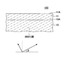
- FIG. 1 is a partial cross-sectional view schematically showing a silicon carbide epitaxial substrate according to one aspect of the present disclosure.
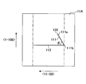
- FIG. 2 is a top view schematically showing a basal plane dislocation in which one end is connected to a threading screw dislocation and another basal plane dislocation connected to the basal plane dislocation.
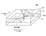
- FIG. 3 is a perspective view (1) schematically showing a basal plane dislocation in which one end is connected to a threading screw dislocation and another basal plane dislocation connected to the basal plane dislocation.
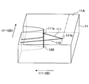
- FIG. 4 is a perspective view (2) schematically showing a basal plane dislocation in which one end is connected to a threading screw dislocation and another basal plane dislocation connected to the basal plane dislocation.
- FIG. 1 is a partial cross-sectional view schematically showing a silicon carbide epitaxial substrate according to one aspect of the present disclosure.
- FIG. 2 is a top view schematically showing a basal plane dislocation in which one end is connected to a threading screw dislocation
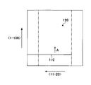
- FIG. 5 is a schematic top view (1) for explaining the basal plane dislocation with one end connected to the threading screw dislocation and the mechanism of the occurrence of another basal plane dislocation.
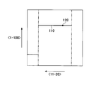
- FIG. 6 is a schematic top view (2) for explaining the mechanism of the occurrence of basal plane dislocations and other basal plane dislocations in which one end is connected to threading screw dislocations.
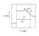
- FIG. 7 is a schematic top view (3) for explaining the basal plane dislocation where one end is connected to the threading screw dislocation and the generation mechanism of the other basal plane dislocation.
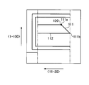
- FIG. 8 is a schematic top view (4) for explaining the basal plane dislocation where one end is connected to the threading screw dislocation and the generation mechanism of the other basal plane dislocation.
- FIG. 9 is a schematic top view (5) for explaining the basal plane dislocation in which one end portion is connected to the threading screw dislocation and the generation mechanism of the other basal plane dislocation.
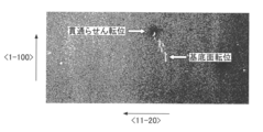
- FIG. 10 is a PL (Photoluminescence) image (1) of the basal plane dislocation and the other basal plane dislocation in which one end is connected to the threading screw dislocation.
- FIG. 11 is a PL image (2) of the basal plane dislocation and the other basal plane dislocation with one end connected to the threading screw dislocation.
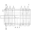
- FIG. 12 is a schematic side view showing an example of the configuration of the film forming apparatus.
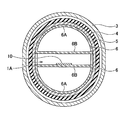
- FIG. 13 is a schematic cross-sectional view showing an example of the configuration of the film forming apparatus.
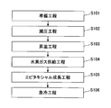
- FIG. 14 is a flowchart illustrating an outline of a method for manufacturing a silicon carbide epitaxial substrate according to one aspect of the present disclosure.
- FIG. 15 is a timing chart showing an example of temperature control and gas flow rate control in the film forming apparatus.
- FIG. 16 is a timing chart showing an example of temperature control and gas flow rate control in a film forming apparatus of a method for manufacturing a silicon carbide epitaxial substrate without a rapid cooling step.
- FIG. 17 is a PL image of dislocations in a silicon carbide epitaxial substrate manufactured by a method for manufacturing a silicon carbide epitaxial substrate without a rapid cooling step.
- FIG. 18 is a flowchart illustrating an outline of a method for manufacturing a silicon carbide semiconductor device according to one aspect of the present disclosure.
- FIG. 15 is a timing chart showing an example of temperature control and gas flow rate control in the film forming apparatus.
- FIG. 16 is a timing chart showing an example of temperature control and gas flow rate control in a film
- FIG. 19 is a process diagram (1) of the method for manufacturing the silicon carbide semiconductor device according to one aspect of the present disclosure.
- FIG. 20 is a process diagram (2) of the method for manufacturing the silicon carbide semiconductor device according to one aspect of the present disclosure.
- FIG. 21 is a process diagram (3) of the method for manufacturing the silicon carbide semiconductor device according to one aspect of the present disclosure.
- Patent Document 1 discloses a silicon carbide epitaxial substrate in which threading edge dislocations and basal plane dislocations connected to the threading edge dislocations are reduced.
- the reliability of the manufactured semiconductor device cannot be sufficiently increased only by reducing the threading edge dislocations and the basal plane dislocations connected to the threading edge dislocations.
- an object of the present disclosure is to provide a silicon carbide epitaxial substrate and a method for manufacturing a silicon carbide semiconductor device capable of reducing basal plane dislocations connected to threading screw dislocations.
- a silicon carbide epitaxial substrate includes a silicon carbide single crystal substrate having a diameter of 100 mm or more and a main surface inclined by more than 0 ° and not more than 8 ° from a ⁇ 0001 ⁇ plane;
- a silicon carbide epitaxial layer having a thickness of 20 ⁇ m or more formed on the silicon carbide epitaxial layer and one end connected to a threading screw dislocation contained in the silicon carbide epitaxial layer;
- the end portion has a basal plane dislocation existing on the surface of the silicon carbide epitaxial layer, and the basal plane dislocation is 20 ° or more and 80 ° or less with respect to the ⁇ 11-20> direction on the ⁇ 0001 ⁇ basal plane. It extends in a direction having an inclination, and the density of the basal plane dislocations is 0.05 / cm 2 or less.
- the inventor of the present application has studied that, in a silicon carbide epitaxial substrate in which a silicon carbide epitaxial layer is formed on a silicon carbide single crystal substrate, one end is connected to a threading screw dislocation, and the other end is We found a basal plane dislocation that becomes the surface of the silicon carbide epitaxial layer.
- This basal plane dislocation has an inclination of 20 ° or more and 80 ° or less with respect to the ⁇ 11-20> direction on the ⁇ 0001 ⁇ basal plane in the direction of the dislocation line.
- the basal plane dislocation is a silicon carbide single crystal substrate having a main surface inclined by more than 0 ° and not more than 8 ° from the ⁇ 0001 ⁇ plane, in particular, having a diameter of 100 mm or more, Is likely to occur when a silicon carbide single crystal substrate having a diameter of 150 mm or more is used. If such basal plane dislocations are present, the basal plane dislocations may proliferate, resulting in a silicon carbide epitaxial substrate containing a large amount of basal plane dislocations. When a semiconductor device is manufactured using such a silicon carbide epitaxial substrate containing many basal plane dislocations, the reliability of the manufactured semiconductor device may be reduced.
- the silicon carbide epitaxial substrate was manufactured using the silicon carbide epitaxial substrate by controlling the number of the basal plane dislocations to be 1 or more and the density of 0.05 / cm 2 or less over the entire surface. There is a possibility that deterioration of the reliability of the semiconductor device can be suppressed.
- the number and density of the basal plane dislocations are determined by analyzing the entire surface of the silicon carbide epitaxial layer using a PL (Photo Luminescence) imaging device and calculating the number of detected basal plane dislocations on the surface of the silicon carbide epitaxial layer. It can be calculated by dividing by the area.
- a PL imaging apparatus for example, a PL imaging apparatus PLIS-100 (manufactured by Photon Design Co., Ltd.) can be used.
- the entire surface does not normally include a region that is not used for a semiconductor device.
- the region not used for the semiconductor device is, for example, a region 3 mm from the edge of the substrate.
- the diameter of the silicon carbide single crystal substrate is 150 mm or more.
- a method for manufacturing a silicon carbide semiconductor device includes a step of preparing a silicon carbide epitaxial substrate and a step of processing the silicon carbide epitaxial substrate.
- the present embodiment an embodiment of the present disclosure (hereinafter referred to as “the present embodiment”) will be described in detail, but the present embodiment is not limited thereto.
- silicon carbide epitaxial substrate 100 in the present embodiment will be described.
- FIG. 1 is a cross-sectional view showing an example of the structure of silicon carbide epitaxial substrate 100 in the present embodiment.
- Silicon carbide epitaxial substrate 100 in the present embodiment is formed on silicon carbide single crystal substrate 10 having a main surface 10A inclined by an off angle ⁇ from a predetermined crystal plane, and main surface 10A of silicon carbide single crystal substrate 10.
- the predetermined crystal plane is preferably a (0001) plane or a (000-1) plane.
- one end portion is connected to a threading screw dislocation, and the other end portion has a basal plane dislocation that becomes the surface of silicon carbide epitaxial layer 11.
- the direction of the dislocation line of the basal plane dislocation has an inclination of 20 ° or more and 80 ° or less with respect to the ⁇ 11-20> direction at the ⁇ 0001 ⁇ basal plane, and the number of basal plane dislocations is 1 or more.
- the dislocation density is 0.05 / cm 2 or less.
- the basal plane dislocation density is 0 (zero).
- the density of the basal plane dislocation is preferably 0.05 pieces / cm 2 or less, more preferably 0.03 pieces / cm 2 or less. It is.
- Basal plane dislocation The basal plane dislocation described above will be described with reference to FIGS. 2 is a top view of silicon carbide epitaxial substrate 100, FIG. 3 is a perspective view, and FIG. 4 is an enlarged perspective view of a main part.
- One end 111 a of basal plane dislocation 111 described above is connected to threading screw dislocation 120, and the other end 111 b becomes surface 11 A of silicon carbide epitaxial layer 11.
- the basal plane dislocation 111 has an inclination in which the angle ⁇ with respect to the ⁇ 11-20> direction is 20 ° or more and 80 ° or less on the ⁇ 0001 ⁇ basal plane.
- Such basal plane dislocations 111 may be connected to other basal plane dislocations 112 from the other end 111b. These basal plane dislocations 111 and other basal plane dislocations 112 have been found as a result of the present inventors' research.
- the silicon carbide epitaxial substrate in the present embodiment is formed by forming a silicon carbide epitaxial layer on a silicon carbide single crystal substrate.
- the silicon carbide single crystal substrate has basal plane dislocations and threading screw dislocations.
- the silicon carbide epitaxial layer formed on the silicon carbide single crystal substrate also has a base as shown in FIG. 5 due to some of the basal plane dislocations and threading screw dislocations in the silicon carbide single crystal substrate. Planar dislocations 110 and threading screw dislocations 120 are generated.
- the basal plane dislocation 110 generated in the silicon carbide epitaxial layer can slide in the ⁇ 1-100> direction on the ⁇ 0001 ⁇ plane serving as the basal plane. Accordingly, the basal plane dislocation 110 slides in the direction indicated by the broken line arrow A. However, when the basal plane dislocation 110 hits the threading screw dislocation 120 as shown in FIG.
- the portion between the threading screw dislocation 120 of the basal plane dislocation 110 and the surface of the silicon carbide epitaxial layer is on the ⁇ 0001 ⁇ basal plane as indicated by the broken arrow B.
- the basal plane dislocation 111 is formed by moving until the angle ⁇ with respect to the ⁇ 11-20> direction is 20 ° or more and 80 ° or less.
- One end 111a of basal plane dislocation 111 is connected to threading screw dislocation 120, and the other end 111b is the surface of the silicon carbide epitaxial layer.
- the other end 111b of the basal plane dislocation 111 extends from the threading screw dislocation 120, reaches the surface of the silicon carbide epitaxial layer, and exists so as to be included in the surface. At this time, another basal plane dislocation 112 is generated from the other end 111 b of the basal plane dislocation 111. With the above mechanism, basal plane dislocations 111 and other basal plane dislocations 112 are generated.
- the other basal plane dislocation 112 is separated from the other end 111b of the basal plane dislocation 111 and slides on the ⁇ 0001 ⁇ plane serving as the basal plane, as indicated by a broken line arrow C. Move in the ⁇ 1-100> direction. Thereafter, another basal plane dislocation 112 is generated again from the other end 111 b of the basal plane dislocation 111, and the other basal plane dislocation 112 is repeatedly separated from the other end 111 b of the basal plane dislocation 111. As a result, as shown in FIG. 9, many basal plane dislocations are generated from one basal plane dislocation 111.
- PL images are PL imaging images of the silicon carbide epitaxial substrate.
- a PL imaging apparatus PLIS-100 manufactured by Photon Design Co., Ltd. was used for the measurement of the PL image.
- a mercury xenon lamp was used as an excitation light source at room temperature, and the silicon carbide epitaxial substrate was irradiated with light passing through a bandpass filter having a wavelength of 313 nm.
- the PL image is an image obtained by transmitting light from a silicon carbide epitaxial substrate through light passing through a filter that transmits light having a wavelength of 750 nm or more.
- FIGS. 10 and 11 are dislocations in the silicon carbide epitaxial layer.
- FIG. 10 shows a state in which the basal plane dislocation 111 extending in an oblique direction and another basal plane dislocation 112 are connected.
- FIG. 11 shows the basal plane dislocation 111 in the ⁇ 11-20> direction and ⁇ 1-100>. Shows zigzag direction.
- a portion in the ⁇ 1-100> direction among the basal plane dislocations that are zigzag is indicated by a bright line.
- the basal plane dislocation was not formed during the formation of the silicon carbide epitaxial layer, but after the formation of the silicon carbide epitaxial layer, the silicon carbide epitaxial substrate was cooled. It is thought to have occurred between. That is, the slip movement of the basal plane dislocation 110 as shown in FIGS. 6 to 9 is considered to occur at a relatively high temperature, specifically, a temperature of 1000 ° C. or more, and occurred in the silicon carbide epitaxial substrate. This is thought to be due to stress. In a silicon carbide epitaxial substrate, if the temperature distribution difference of the silicon carbide epitaxial substrate is large, the stress generated in the silicon carbide epitaxial substrate also increases.
- the step of increasing the temperature distribution difference of the silicon carbide epitaxial substrate includes a cooling step of the silicon carbide epitaxial substrate. In this cooling step, stress is particularly likely to occur in the silicon carbide epitaxial substrate.
- the silicon carbide epitaxial layer is formed at a very high temperature of about 1600 ° C. In this case, although the temperature is high, the uniformity of the temperature distribution is relatively high.
- the silicon carbide epitaxial substrate is cooled. In this case, the whole is not cooled at a uniform temperature, and the temperature distribution tends to vary.
- the silicon carbide epitaxial substrate if the time in which the temperature distribution varies is long, it is considered that the basal plane dislocations 111 occur and the number of other basal plane dislocations 112 increases. .
- the basal plane dislocations 111 are not so often seen on a substrate having a small silicon carbide single crystal substrate 10, but are prominently generated when the substrate becomes large.
- the silicon carbide single crystal substrate 10 is remarkably generated when the size thereof is 100 mm or more, and further 150 mm (for example, 6 inches) or more. This is considered to be because, if the area of the silicon carbide single crystal substrate 10 is large, the difference in temperature distribution becomes large at the time of cooling, and stress is easily generated accordingly.
- the silicon carbide epitaxial substrate in the present embodiment is obtained by forming a silicon carbide epitaxial layer and then rapidly cooling the silicon carbide epitaxial substrate by blowing a gas. That is, by rapidly cooling after the silicon carbide epitaxial layer is formed, before the basal plane dislocation slip movement and the basal plane dislocation growth occur, until the basal plane dislocation slip movement and proliferation are less than 1000 ° C. To shorten the time. Thereby, a silicon carbide epitaxial substrate with few basal plane dislocations 111 and other basal plane dislocations 112 can be produced.
- FIG. 12 is a schematic side view showing an example of the configuration of the film forming apparatus.
- 13 is a cross-sectional view taken along one-dot chain line 12A-12B in FIG.
- the film forming apparatus 1 shown in FIGS. 12 and 13 is a horizontal hot wall CVD (chemical vapor deposition) apparatus.
- the film forming apparatus 1 includes a heating element 6, a heat insulating material 5, a quartz tube 4, and an induction heating coil 3.
- the heating element 6 is made of, for example, carbon.
- each heating element 6 has a semi-cylindrical hollow structure including a curved surface portion 6A and a flat portion 6B.
- the two flat portions 6B are arranged to face each other, and a space surrounded by the two flat portions 6B is a chamber 1A in which the silicon carbide single crystal substrate 10 is installed.
- the chamber 1A is also referred to as a “gas flow channel”.
- the heat insulating material 5 is arrange
- the chamber 1A is thermally insulated from the outside of the film forming apparatus 1 by a heat insulating material 5.
- the quartz tube 4 is disposed so as to surround the outer periphery of the heat insulating material 5.
- the induction heating coil 3 is wound along the outer periphery of the quartz tube 4. In the film forming apparatus 1, by supplying an alternating current to the induction heating coil 3, the heating element 6 is induction heated and the temperature in the chamber 1 ⁇ / b> A can be controlled. At this time, the quartz tube 4 is hardly heated because it is insulated by the heat insulating material 5.
- FIG. 14 is a flowchart showing an outline of a method for manufacturing the silicon carbide epitaxial substrate of the present embodiment.
- the silicon carbide epitaxial substrate manufacturing method of the present embodiment includes a preparation step (S101), a pressure reduction step (S102), a temperature raising step (S103), a hydrogen gas supply step (S104), and an epitaxial growth step. (S105) and a rapid cooling step (S106).
- basal plane dislocations in the silicon carbide single crystal substrate 10 can be reduced by performing a rapid cooling step (S106) after the epitaxial growth step (S105).
- S106 rapid cooling step
- a silicon carbide single crystal substrate 10 is prepared.
- Silicon carbide single crystal substrate 10 is produced, for example, by slicing an ingot made of a silicon carbide single crystal. For the slice, for example, a wire saw is used.
- the polytype of silicon carbide is preferably 4H. This is because it is superior to other polytypes in electron mobility, dielectric breakdown field strength, and the like.
- Silicon carbide single crystal substrate 10 has a diameter of 100 mm or more, more preferably 150 mm or more (for example, 6 inches or more). The larger the diameter, the more advantageous for the manufacturing cost reduction of the semiconductor device.
- Silicon carbide single crystal substrate 10 has a main surface 10A on which silicon carbide epitaxial layer 11 will be grown later.
- Silicon carbide single crystal substrate 10 has an off angle ⁇ of more than 0 ° and not more than 8 °. That is, the main surface 10A is a surface that is inclined from the predetermined crystal plane by an off angle ⁇ of more than 0 ° and not more than 8 °.
- the predetermined crystal plane is preferably a (0001) plane or a (000-1) plane. That is, the predetermined crystal plane is preferably a ⁇ 0001 ⁇ plane.
- the direction in which the off angle is provided is the ⁇ 11-20> direction.
- the off angle ⁇ is more preferably 2 ° or more and 7 ° or less, further preferably 3 ° or more and 6 ° or less, and most preferably 3 ° or more and 5 ° or less. This is because by setting the off angle in such a range, the balance between the suppression of different polytypes and the growth rate is maintained. Subsequent steps are performed in the film forming apparatus 1.
- the silicon carbide single crystal substrate 10 is placed in the chamber 1A of the film forming apparatus 1, and the inside of the chamber 1A is decompressed. Silicon carbide single crystal substrate 10 is placed on a susceptor (not shown) in chamber 1A.
- the susceptor may be provided with a SiC coating or the like.
- FIG. 15 is a timing chart showing control of the temperature and gas flow rate in the chamber 1A after the decompression step (S102).
- the depressurization step (S102) is performed from time t1 when pressure reduction in the chamber 1A is started after the silicon carbide single crystal substrate 10 is installed in the chamber 1A to time t2 when the pressure in the chamber 1A reaches the target value. It corresponds to between.
- the target value of the pressure in the decompression step (S102) is, for example, about 1 ⁇ 10 ⁇ 6 Pa.
- the temperature in the chamber 1A of the film forming apparatus 1 is heated to the second temperature T2.
- the temperature rise in the chamber 1A is started from the time point t2, the temperature in the chamber 1A reaches the first temperature T1 at the time point t3, and further, the temperature in the chamber 1A is changed to the first temperature at the time point t4.
- a temperature T2 of 2 is reached.
- the first temperature T1 is 1100 ° C., for example.
- the second temperature T2 is preferably 1500 ° C. or higher and 1700 ° C. or lower.
- the second temperature T2 is more preferably 1520 ° C. or higher and 1680 ° C. or lower, particularly preferably 1550 ° C. or higher and 1650 ° C. or lower. In this embodiment, it is 1630 degreeC.
- the hydrogen (H 2 ) gas is supplied into the chamber 1A from the time t3 when the temperature in the chamber 1A reaches the first temperature T1, and the chamber
- the pressure in 1A is set to a predetermined pressure, for example, 8 kPa.
- the supply of hydrogen gas starts at time t3, gradually increases the flow rate of hydrogen gas, and supplies the hydrogen gas at 120 slm at time t4.
- the temperature raising step (S103) is continued until the temperature in the chamber 1A of the film forming apparatus 1 reaches the second temperature T2. After the temperature in the chamber 1A of the film forming apparatus 1 reaches the second temperature T2, an epitaxial growth step (S105) is performed.
- hydrocarbon gas and silane (SiH 4 ) gas are supplied into the chamber 1A of the film forming apparatus 1 together with hydrogen gas.
- the predetermined pressure in the chamber 1A in the epitaxial growth step (S105) is, for example, 8 kPa.
- hydrocarbon gas examples include methane (CH 4 ) gas, ethane (C 2 H 6 ) gas, propane (C 3 H 8 ) gas, butane (C 4 H 10 ) gas, acetylene (C 2 H 2 ) gas, and the like. Can be used. These hydrocarbon gas may be used individually by 1 type, and 2 or more types may be mixed and used for it. That is, the hydrocarbon gas preferably contains one or more selected from the group consisting of methane gas, ethane gas, propane gas, butane gas, and acetylene gas.
- the flow rate of the hydrocarbon gas is preferably 5 sccm or more and 30 sccm or less. In the present embodiment, for example, 15 sccm of propane gas is supplied as the hydrocarbon gas.
- the flow rate of the silane gas is not particularly limited, but the ratio (C / Si) between the number of carbon (C) atoms contained in the hydrocarbon gas and the number of silicon (Si) atoms contained in the silane gas is 0.5 or more. It is preferable to adjust the flow rate of the silane gas so as to be 2.0 or less. This is because SiC having an appropriate stoichiometric ratio is epitaxially grown. In this embodiment, for example, 45 sccm of silane gas is supplied.
- nitrogen (N 2 ) or the like may be supplied as a dopant.
- the epitaxial growth step (S105) is performed until time t5 in accordance with the target thickness of silicon carbide epitaxial layer 11.
- a rapid cooling step (S106) is performed.
- hydrogen or argon (Ar) is sprayed onto the silicon carbide epitaxial substrate after the epitaxial growth to rapidly cool it.
- the flow rate of hydrogen gas is increased, and hydrogen gas is sprayed onto the silicon carbide epitaxial substrate on which epitaxial growth has been completed.
- the pressure in the chamber 1A may exceed 8 kPa.
- the third temperature T3 at 10 minutes after the start of cooling, that is, at the time t6 after 10 minutes from the time t5 can be about 700 ° C. Therefore, since the temperature can be made 1000 ° C.
- the density of basal plane dislocations 111 in the silicon carbide epitaxial substrate can be 0.05 / cm 2 or less.
- silicon carbide epitaxial substrate 100 in the present embodiment can be manufactured.
- FIG. 16 shows a timing chart showing the control of the temperature and gas flow rate in the chamber 1A after the decompression step in this case.
- the difference from the manufacturing method of the present embodiment shown in FIG. 15 is that cooling is normally performed without rapidly cooling the silicon carbide epitaxial substrate after the epitaxial growth is completed after time t5 when the epitaxial growth step is completed.
- cooling is performed at a hydrogen gas flow rate of 100 slm from the time t5 when the epitaxial growth is completed.
- the predetermined pressure in the chamber 1A at this time is, for example, 8 kPa.
- the temperature at the time point t16 after 10 minutes from the time point t5 is about 1200 ° C. and is 1000 ° C. or higher.
- the basal plane dislocation is slipping and it is assumed that the basal plane dislocation 111 and other basal plane dislocations 112 increase.
- the cooling is further performed, and the supply of hydrogen gas is stopped at time t17 when the temperature reaches 600 ° C.
- the chamber 1A is opened to the atmosphere, the chamber 1A is returned to atmospheric pressure, and the silicon carbide epitaxial substrate is taken out from the chamber 1A. .
- FIG. 17 shows a PL image of the silicon carbide epitaxial substrate produced by the manufacturing method of the timing chart shown in FIG. In the manufacturing method of the timing chart shown in FIG. 16, since it is about 1200 ° C. and 1000 ° C. or more even after 10 minutes after the epitaxial growth is completed, the basal plane dislocation slips, and as shown in FIG. A large number of dislocations (about 40 / cm 2 ) are observed.
- the basal plane dislocation can be made to be 1000 ° C. or less in which the basal plane dislocations hardly slide in a short time. Therefore, basal plane dislocations can be reduced as compared with the silicon carbide epitaxial substrate shown in FIG.
- the method for manufacturing a silicon carbide semiconductor device mainly includes an epitaxial substrate preparation step (S210: FIG. 18) and a substrate processing step (S220: FIG. 18).
- a silicon carbide epitaxial substrate preparation step (S210: FIG. 18) is performed. Specifically, a silicon carbide epitaxial substrate is prepared by the above-described method for manufacturing a silicon carbide epitaxial substrate.
- a substrate processing step (S220: FIG. 18) is performed.
- a silicon carbide semiconductor device is manufactured by processing a silicon carbide epitaxial substrate.
- “Processing” includes, for example, various processes such as ion implantation, heat treatment, etching, oxide film formation, electrode formation, and dicing. That is, the substrate processing step may include at least one of ion implantation, heat treatment, etching, oxide film formation, electrode formation, and dicing.
- the substrate processing step includes an ion implantation step (S221: FIG. 18), an oxide film formation step (S222: FIG. 18), an electrode formation step (S223: FIG. 18), and a dicing step (S224: FIG. 18). including.
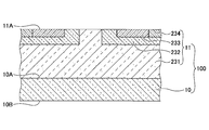
- an ion implantation step (S221: FIG. 18) is performed.
- a p-type impurity such as aluminum (Al) is implanted into the surface 11A on which a mask (not shown) having an opening is formed.
- body region 232 having p-type conductivity is formed.
- an n-type impurity such as phosphorus (P) is implanted into a predetermined position in body region 232.
- a source region 233 having n-type conductivity is formed.
- a p-type impurity such as aluminum is implanted into a predetermined position in the source region 233.
- a contact region 234 having a p-type conductivity is formed (see FIG. 19).
- Ion implantation may be performed by heating silicon carbide epitaxial substrate 100 to about 300 ° C. or more and 600 ° C. or less.
- activation annealing is performed on silicon carbide epitaxial substrate 100.
- the atmosphere of activation annealing may be, for example, an argon (Ar) atmosphere.
- the activation annealing temperature may be about 1800 ° C., for example.
- the activation annealing time may be about 30 minutes, for example.
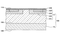
- oxide film forming step (S222: FIG. 18) is performed.
- silicon carbide epitaxial substrate 100 is heated in an atmosphere containing oxygen, whereby oxide film 236 is formed on surface 11A (see FIG. 20).
- Oxide film 236 is made of, for example, silicon dioxide (SiO 2 ).
- the oxide film 236 functions as a gate insulating film.
- the temperature of the thermal oxidation treatment may be about 1300 ° C., for example.
- the thermal oxidation treatment time may be about 30 minutes, for example.
- heat treatment may be further performed in a nitrogen atmosphere.
- the heat treatment may be performed at about 1100 ° C. for about 1 hour in an atmosphere such as nitric oxide (NO) or nitrous oxide (N 2 O).
- heat treatment may be performed in an argon atmosphere.
- the heat treatment may be performed in an argon atmosphere at about 1100 to 1500 ° C. for about 1 hour.
- the first electrode 241 is formed on the oxide film 236.
- the first electrode 241 functions as a gate electrode.
- the first electrode 241 is formed by, for example, a CVD method.
- the first electrode 241 is made of, for example, polysilicon containing impurities and having conductivity.
- the first electrode 241 is formed at a position facing the source region 233 and the body region 232.
- Interlayer insulating film 237 that covers the first electrode 241 is formed.
- Interlayer insulating film 237 is formed by, for example, a CVD method.
- Interlayer insulating film 237 is made of, for example, silicon dioxide.
- the interlayer insulating film 237 is formed so as to be in contact with the first electrode 241 and the oxide film 236.
- the oxide film 236 and the interlayer insulating film 237 at predetermined positions are removed by etching. As a result, the source region 233 and the contact region 234 are exposed from the oxide film 236.
- the second electrode 242 is formed on the exposed portion by sputtering.
- the second electrode 242 functions as a source electrode.
- the second electrode 242 is made of, for example, titanium, aluminum, silicon, or the like.
- second electrode 242 and silicon carbide epitaxial substrate 100 are heated at a temperature of about 900 to 1100 ° C., for example. Thereby, second electrode 242 and silicon carbide epitaxial substrate 100 come into ohmic contact.
- the wiring layer 238 is formed so as to be in contact with the second electrode 242.
- Wiring layer 238 is made of, for example, a material containing aluminum.
- a passivation protection film (not shown) is formed on the wiring layer 238 by, for example, plasma CVD.
- the passivation protection film includes, for example, a SiN film.
- a part of the passivation protective film is etched to the wiring layer 238, and an opening is formed in the passivation protective film.
- back grinding is performed on back surface 10 ⁇ / b> B of silicon carbide single crystal substrate 10. Thereby, silicon carbide single crystal substrate 10 is thinned.
- the third electrode 243 is formed on the back surface 10B.
- the third electrode 243 functions as a drain electrode.
- the third electrode 243 is made of, for example, an alloy containing nickel and silicon (for example, NiSi).
- a dicing step (S224: FIG. 18) is performed.
- silicon carbide epitaxial substrate 100 is diced along a dicing line, whereby silicon carbide epitaxial substrate 100 is divided into a plurality of semiconductor chips.
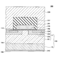
- silicon carbide semiconductor device 300 is manufactured (see FIG. 21).
- the method for manufacturing the silicon carbide semiconductor device according to the present disclosure has been described by exemplifying the MOSFET, but the manufacturing method according to the present disclosure is not limited to this.
- the manufacturing method according to the present disclosure is applicable to various silicon carbide semiconductor devices such as IGBT (Insulated Gate Bipolar Transistor), SBD (Schottky Barrier Diode), thyristor, GTO (Gate Turn Off thyristor), and PiN diode.
- IGBT Insulated Gate Bipolar Transistor
- SBD Schottky Barrier Diode
- thyristor thyristor
- GTO Gate Turn Off thyristor
- PiN diode PiN diode
Landscapes
- Engineering & Computer Science (AREA)
- Chemical & Material Sciences (AREA)
- Power Engineering (AREA)
- Microelectronics & Electronic Packaging (AREA)
- Physics & Mathematics (AREA)
- Computer Hardware Design (AREA)
- Condensed Matter Physics & Semiconductors (AREA)
- General Physics & Mathematics (AREA)
- Ceramic Engineering (AREA)
- Materials Engineering (AREA)
- Crystallography & Structural Chemistry (AREA)
- Manufacturing & Machinery (AREA)
- Metallurgy (AREA)
- Organic Chemistry (AREA)
- General Chemical & Material Sciences (AREA)
- Chemical Kinetics & Catalysis (AREA)
- Inorganic Chemistry (AREA)
- Mechanical Engineering (AREA)
- Crystals, And After-Treatments Of Crystals (AREA)
- Recrystallisation Techniques (AREA)
Abstract
L'invention concerne un substrat épitaxial de carbure de silicium qui comprend : un substrat monocristallin de carbure de silicium qui a une surface principale inclinée à plus de 0° et à ou moins de 8º par rapport au plan {0001}, et qui a un diamètre de 100 mm ou plus; une couche épitaxiale de carbure de silicium qui est formée sur la surface principale et a une épaisseur de 20 µm ou plus; et une dislocation de plan de base qui est contenue dans la couche épitaxiale de carbure de silicium, une extrémité de la dislocation de plan de base étant connectée à une dislocation de vis de filetage contenue dans la couche épitaxiale de carbure de silicium, tandis que l'autre extrémité de la dislocation de plan de base se situe sur la surface de la couche épitaxiale de carbure de silicium. La dislocation de plan de base s'étend dans une direction qui est inclinée à 20 à 80° compris dans la direction <11-20> sur le plan de base {0001}. La densité de la dislocation du plan de base est de 0,05/cm2 ou moins.
Priority Applications (4)
| Application Number | Priority Date | Filing Date | Title |
|---|---|---|---|
| JP2017544970A JP6233555B1 (ja) | 2016-10-04 | 2017-06-05 | 炭化珪素エピタキシャル基板及び炭化珪素半導体装置の製造方法 |
| US16/333,308 US10714572B2 (en) | 2016-10-04 | 2017-06-05 | Silicon carbide epitaxial substrate and method for manufacturing a silicon carbide semiconductor device |
| CN201780061273.9A CN109791879B (zh) | 2016-10-04 | 2017-06-05 | 碳化硅外延衬底和制造碳化硅半导体器件的方法 |
| DE112017005034.0T DE112017005034T5 (de) | 2016-10-04 | 2017-06-05 | Siliziumkarbid-epitaxiesubstrat und verfahren zur herstellung einer siliziumkarbid-halbleitervorrichtung |
Applications Claiming Priority (2)
| Application Number | Priority Date | Filing Date | Title |
|---|---|---|---|
| JP2016-196636 | 2016-10-04 | ||
| JP2016196636 | 2016-10-04 |
Publications (1)
| Publication Number | Publication Date |
|---|---|
| WO2018066173A1 true WO2018066173A1 (fr) | 2018-04-12 |
Family
ID=61831463
Family Applications (1)
| Application Number | Title | Priority Date | Filing Date |
|---|---|---|---|
| PCT/JP2017/020887 WO2018066173A1 (fr) | 2016-10-04 | 2017-06-05 | Substrat épitaxial de carbure de silicium, et procédé de fabrication d'un dispositif à semi-conducteur à base de carbure de silicium |
Country Status (5)
| Country | Link |
|---|---|
| US (1) | US10714572B2 (fr) |
| JP (1) | JP6891758B2 (fr) |
| CN (1) | CN109791879B (fr) |
| DE (1) | DE112017005034T5 (fr) |
| WO (1) | WO2018066173A1 (fr) |
Cited By (1)
| Publication number | Priority date | Publication date | Assignee | Title |
|---|---|---|---|---|
| WO2024080071A1 (fr) * | 2022-10-11 | 2024-04-18 | 住友電気工業株式会社 | Substrat de cristal de carbure de silicium, substrat épitaxial et procédé de fabrication de dispositif à semi-conducteur |
Families Citing this family (5)
| Publication number | Priority date | Publication date | Assignee | Title |
|---|---|---|---|---|
| US12020924B2 (en) | 2018-05-09 | 2024-06-25 | Sumitomo Electric Industries, Ltd. | Silicon carbide epitaxial substrate and method of manufacturing silicon carbide semiconductor device |
| JP6585799B1 (ja) | 2018-10-15 | 2019-10-02 | 昭和電工株式会社 | SiC基板の評価方法及びSiCエピタキシャルウェハの製造方法 |
| JP2023508691A (ja) | 2019-12-27 | 2023-03-03 | ウルフスピード インコーポレイテッド | 大口径炭化ケイ素ウェハ |
| US12125701B2 (en) * | 2020-12-15 | 2024-10-22 | Wolfspeed, Inc. | Large dimension silicon carbide single crystalline materials with reduced crystallographic stress |
| CN113388888B (zh) * | 2021-06-22 | 2022-07-12 | 山东天岳先进科技股份有限公司 | 一种碳化硅晶体、其使用的籽晶及籽晶的制备方法 |
Citations (2)
| Publication number | Priority date | Publication date | Assignee | Title |
|---|---|---|---|---|
| JP2015002207A (ja) * | 2013-06-13 | 2015-01-05 | 昭和電工株式会社 | SiCエピタキシャルウェハ及びその製造方法 |
| JP2016165004A (ja) * | 2014-10-01 | 2016-09-08 | 住友電気工業株式会社 | 炭化珪素エピタキシャル基板 |
Family Cites Families (11)
| Publication number | Priority date | Publication date | Assignee | Title |
|---|---|---|---|---|
| US7314520B2 (en) * | 2004-10-04 | 2008-01-01 | Cree, Inc. | Low 1c screw dislocation 3 inch silicon carbide wafer |
| JP5273741B2 (ja) * | 2007-09-12 | 2013-08-28 | 昭和電工株式会社 | エピタキシャルSiC単結晶基板及びエピタキシャルSiC単結晶基板の製造方法 |
| CN101803100A (zh) | 2007-09-12 | 2010-08-11 | 大金工业株式会社 | 电解液 |
| JP2010184833A (ja) * | 2009-02-12 | 2010-08-26 | Denso Corp | 炭化珪素単結晶基板および炭化珪素単結晶エピタキシャルウェハ |
| JP5914366B2 (ja) | 2010-03-01 | 2016-05-11 | ザ ユニヴァーシティ オヴ ブリティッシュ コロンビア | 誘導体化超分岐ポリグリセロール類 |
| JP6025306B2 (ja) * | 2011-05-16 | 2016-11-16 | 株式会社豊田中央研究所 | SiC単結晶、SiCウェハ及び半導体デバイス |
| JP5958949B2 (ja) * | 2011-05-26 | 2016-08-02 | 一般財団法人電力中央研究所 | 炭化珪素基板、炭化珪素ウェハ、炭化珪素ウェハの製造方法及び炭化珪素半導体素子 |
| US8940614B2 (en) * | 2013-03-15 | 2015-01-27 | Dow Corning Corporation | SiC substrate with SiC epitaxial film |
| JP2016166112A (ja) * | 2015-03-10 | 2016-09-15 | 株式会社東芝 | 半導体基板及び半導体装置 |
| WO2017018533A1 (fr) * | 2015-07-29 | 2017-02-02 | 新日鐵住金株式会社 | Procédé de production de plaquette de monocristal de carbure de silicium épitaxiale |
| US20170321345A1 (en) * | 2016-05-06 | 2017-11-09 | Ii-Vi Incorporated | Large Diameter Silicon Carbide Single Crystals and Apparatus and Method of Manufacture Thereof |
-
2017
- 2017-06-05 US US16/333,308 patent/US10714572B2/en active Active
- 2017-06-05 DE DE112017005034.0T patent/DE112017005034T5/de active Pending
- 2017-06-05 CN CN201780061273.9A patent/CN109791879B/zh active Active
- 2017-06-05 WO PCT/JP2017/020887 patent/WO2018066173A1/fr active Application Filing
- 2017-10-17 JP JP2017200837A patent/JP6891758B2/ja active Active
Patent Citations (2)
| Publication number | Priority date | Publication date | Assignee | Title |
|---|---|---|---|---|
| JP2015002207A (ja) * | 2013-06-13 | 2015-01-05 | 昭和電工株式会社 | SiCエピタキシャルウェハ及びその製造方法 |
| JP2016165004A (ja) * | 2014-10-01 | 2016-09-08 | 住友電気工業株式会社 | 炭化珪素エピタキシャル基板 |
Cited By (1)
| Publication number | Priority date | Publication date | Assignee | Title |
|---|---|---|---|---|
| WO2024080071A1 (fr) * | 2022-10-11 | 2024-04-18 | 住友電気工業株式会社 | Substrat de cristal de carbure de silicium, substrat épitaxial et procédé de fabrication de dispositif à semi-conducteur |
Also Published As
| Publication number | Publication date |
|---|---|
| JP6891758B2 (ja) | 2021-06-18 |
| CN109791879A (zh) | 2019-05-21 |
| US10714572B2 (en) | 2020-07-14 |
| CN109791879B (zh) | 2023-07-25 |
| DE112017005034T5 (de) | 2019-06-27 |
| US20190245044A1 (en) | 2019-08-08 |
| JP2018070440A (ja) | 2018-05-10 |
Similar Documents
| Publication | Publication Date | Title |
|---|---|---|
| WO2018066173A1 (fr) | Substrat épitaxial de carbure de silicium, et procédé de fabrication d'un dispositif à semi-conducteur à base de carbure de silicium | |
| JP7052851B2 (ja) | 炭化珪素エピタキシャル基板および炭化珪素半導体装置の製造方法 | |
| WO2017138247A1 (fr) | Substrat épitaxial en carbure de silicium et procédé permettant de fabriquer un dispositif à semi-conducteur en carbure de silicium | |
| US10697086B2 (en) | Method for manufacturing silicon carbide epitaxial substrate, method for manufacturing silicon carbide semiconductor device, and apparatus for manufacturing silicon carbide epitaxial substrate | |
| JP6856156B2 (ja) | 炭化珪素エピタキシャル基板および炭化珪素半導体装置の製造方法 | |
| US10811500B2 (en) | Silicon carbide epitaxial substrate and method for manufacturing silicon carbide semiconductor device | |
| WO2018142668A1 (fr) | Substrat épitaxial de carbure de silicium et procédé de fabrication d'un dispositif à semi-conducteur en carbure de silicium | |
| JP6233555B1 (ja) | 炭化珪素エピタキシャル基板及び炭化珪素半導体装置の製造方法 | |
| US12020927B2 (en) | Method for manufacturing silicon carbide epitaxial substrate and method for manufacturing silicon carbide semiconductor device | |
| JP7415558B2 (ja) | 炭化珪素エピタキシャル基板および炭化珪素半導体装置の製造方法 | |
| US20220367643A1 (en) | Method of manufacturing a silicon carbide epitaxial substrate | |
| WO2018123148A1 (fr) | Substrat épitaxique au carbure de silicium et procédé de production d'un dispositif semi-conducteur au carbure de silicium | |
| JP6468291B2 (ja) | 炭化珪素エピタキシャル基板、炭化珪素エピタキシャル基板の製造方法および炭化珪素半導体装置の製造方法 | |
| US11735415B2 (en) | Method for manufacturing silicon carbide epitaxial substrate and method for manufacturing silicon carbide semiconductor device | |
| JP6061060B1 (ja) | 炭化珪素エピタキシャル基板および炭化珪素半導体装置の製造方法 |
Legal Events
| Date | Code | Title | Description |
|---|---|---|---|
| WWE | Wipo information: entry into national phase |
Ref document number: 2017544970 Country of ref document: JP |
|
| 121 | Ep: the epo has been informed by wipo that ep was designated in this application |
Ref document number: 17858013 Country of ref document: EP Kind code of ref document: A1 |
|
| 122 | Ep: pct application non-entry in european phase |
Ref document number: 17858013 Country of ref document: EP Kind code of ref document: A1 |
