WO2018056313A1 - 複層金属ボール - Google Patents
複層金属ボール Download PDFInfo
- Publication number
- WO2018056313A1 WO2018056313A1 PCT/JP2017/033931 JP2017033931W WO2018056313A1 WO 2018056313 A1 WO2018056313 A1 WO 2018056313A1 JP 2017033931 W JP2017033931 W JP 2017033931W WO 2018056313 A1 WO2018056313 A1 WO 2018056313A1
- Authority
- WO
- WIPO (PCT)
- Prior art keywords
- ball
- layer
- plating layer
- intermediate plating
- alloy
- Prior art date
- Legal status (The legal status is an assumption and is not a legal conclusion. Google has not performed a legal analysis and makes no representation as to the accuracy of the status listed.)
- Ceased
Links
Images


Classifications
-
- B—PERFORMING OPERATIONS; TRANSPORTING
- B22—CASTING; POWDER METALLURGY
- B22F—WORKING METALLIC POWDER; MANUFACTURE OF ARTICLES FROM METALLIC POWDER; MAKING METALLIC POWDER; APPARATUS OR DEVICES SPECIALLY ADAPTED FOR METALLIC POWDER
- B22F1/00—Metallic powder; Treatment of metallic powder, e.g. to facilitate working or to improve properties
-
- B—PERFORMING OPERATIONS; TRANSPORTING
- B23—MACHINE TOOLS; METAL-WORKING NOT OTHERWISE PROVIDED FOR
- B23K—SOLDERING OR UNSOLDERING; WELDING; CLADDING OR PLATING BY SOLDERING OR WELDING; CUTTING BY APPLYING HEAT LOCALLY, e.g. FLAME CUTTING; WORKING BY LASER BEAM
- B23K35/00—Rods, electrodes, materials, or media, for use in soldering, welding, or cutting
- B23K35/22—Rods, electrodes, materials, or media, for use in soldering, welding, or cutting characterised by the composition or nature of the material
- B23K35/24—Selection of soldering or welding materials proper
- B23K35/26—Selection of soldering or welding materials proper with the principal constituent melting at less than 400°C
-
- C—CHEMISTRY; METALLURGY
- C22—METALLURGY; FERROUS OR NON-FERROUS ALLOYS; TREATMENT OF ALLOYS OR NON-FERROUS METALS
- C22C—ALLOYS
- C22C13/00—Alloys based on tin
-
- C—CHEMISTRY; METALLURGY
- C22—METALLURGY; FERROUS OR NON-FERROUS ALLOYS; TREATMENT OF ALLOYS OR NON-FERROUS METALS
- C22C—ALLOYS
- C22C13/00—Alloys based on tin
- C22C13/02—Alloys based on tin with antimony or bismuth as the next major constituent
-
- C—CHEMISTRY; METALLURGY
- C22—METALLURGY; FERROUS OR NON-FERROUS ALLOYS; TREATMENT OF ALLOYS OR NON-FERROUS METALS
- C22C—ALLOYS
- C22C19/00—Alloys based on nickel or cobalt
- C22C19/03—Alloys based on nickel or cobalt based on nickel
Definitions
- the present invention relates to a multilayer metal ball used when a semiconductor element, a package, a circuit board, and the like are stacked and connected.
- connection material used for semiconductor mounting is required to have many functions such as electrical conduction or structural connection of a substrate.
- the connection materials are roughly classified into a semiconductor internal connection for connecting the electrode of the semiconductor element and the substrate, and a semiconductor external connection for connecting the semiconductor package on which the semiconductor element is mounted and the circuit board.
- ball connection For the internal connection of semiconductor mounting, balls are increasingly used to join the electrodes of semiconductor elements and resin substrates. Compared to conventional wire connection, connection using a ball (hereinafter also referred to as ball connection) is advantageous for high density connection corresponding to high integration and high frequency. For external connection of semiconductor packages, ball connection has recently been used in order to adapt to surface mounting suitable for miniaturization and thinning.
- ⁇ Solder is often used for these ball materials. By melting the solder balls by the reflow process, it is possible to obtain the bonding strength relatively easily.
- three-dimensional packaging such as stacked structures and MCM (Multi Chip Module) has evolved. Laminating a plurality of elements or semiconductor packages in the vertical direction is advantageous in reducing the mounting area. In such three-dimensional mounting, it is important to control the stacking interval. Recently, a hybrid structure in which another element is incorporated in the vertical distance between the stacked elements and the substrate has been developed. At this time, it is important to control the stacking interval because it affects the performance and quality of the product.
- a connection using a ball can be used for installation and fixing of a laminated semiconductor element and a semiconductor package (hereinafter collectively referred to as a laminated component) on a substrate.
- a bonding function for connecting the laminated components and a spacer function for controlling the lamination interval (height) are required.
- the stacked electrodes may be electrically connected by ball bumps.
- a solder ball or a Cu core ball whose surface is coated with solder can be used (see, for example, Patent Document 1 and Patent Document 2).
- Solder balls are suitable for joining because they can be easily joined by melting, but they are easily deformed during ball joining because of their low melting points. For this reason, it is difficult for the solder balls to adjust the interval between the laminated components or between the laminated components and the substrate (hereinafter referred to as the laminated interval), and the spacer function is inferior. In order to assemble the laminated parts stably, it is important to maintain this lamination interval with a predetermined size with high accuracy. In this regard, in the multi-layer metal ball having Cu as the core ball, Cu having a high melting point and being hard to deform is used as the core ball, so that the spacer function is excellent and the stacking interval can be adjusted.
- the multi-layer metal ball has a reduced sphericity.
- the bonding reliability may be lowered, for example, the stability is lowered and the bonding is liable to occur.
- an object of the present invention is to obtain a multilayer metal ball having an excellent spacer function and high bonding reliability.
- the multilayer metal ball according to the present invention includes a core ball made of Sn or Sn alloy, an intermediate plating layer made of Ni or Ni alloy and covering the core ball, and an outer layer made of Sn or Sn alloy and covering the intermediate plating layer
- the thickness of the intermediate plating layer is 3 ⁇ m or more and 100 ⁇ m or less.
- the core ball is formed of Sn or an Sn alloy, and the intermediate plating layer is selected to have an optimum thickness, so that a multi-layer metal ball having good sphericity can be formed, and high bonding reliability can be realized.
- the intermediate plating layer formed thick on the surface of the core ball can suppress the ball deformation at the time of load application or heating in the reflow process, thereby realizing a stable spacer function. Therefore, it is possible to provide a multi-layered metal ball having an excellent spacer function and high bonding reliability.
- the advantages of using a core ball made of Sn or Sn alloy are that the manufacturing process for forming the ball into a ball shape is simple, the ball size can be easily changed, and the ball size can be controlled with high precision. And stabilization of the shape such as surface smoothness.
- Cu has a higher melting point than solder, so a special melting device that melts at high temperatures is required, and ball size variations tend to occur, and elliptical and flat balls are formed. There were problems such as cases.
- core balls of multi-layer metal balls are made of Sn or Sn alloy
- the core balls will melt in the reflow process performed at the time of ball bonding, so that they can withstand the weight of the laminated substrates and load loads
- the core ball of the multi-layer metal ball is formed of Sn or Sn alloy, Ni on the core ball surface, Alternatively, it has been found effective to form a three-layer structure in which an intermediate plating layer made of a Ni alloy is formed thick and an outer layer made of Sn or Sn alloy is further provided on the surface of the intermediate plating layer. Furthermore, it has been found that control of the composition and hardness of the core ball and the intermediate plating layer is effective.
- FIG. 1 shows a cross-sectional structure of a multilayer metal ball according to the present invention.
- the multilayer metal ball 1 has a configuration in which a core ball 2, an intermediate plating layer 3, and an outer layer 4 are provided in this order from the inside toward the surface.
- the outer layer 4 and the core ball 2 are made of Sn or an Sn alloy, and an intermediate plating layer 3 mainly composed of Ni is provided between the outer layer 4 and the core ball 2, and the intermediate plating is performed.
- the layer 3 is formed thick.
- FIG. 2 shows an example of a mounting structure in which a plurality of semiconductor elements 6 and 9 are stacked on a circuit board (also simply referred to as a board) 7.
- the semiconductor element 9 is connected to the electrode 5a of the circuit board 7 via the bump 10.
- the multilayer metal ball 1 is used to connect the semiconductor element 6 and the circuit board 7. ing.
- the multi-layer metal ball 1 is required to have a high spacer function.
- the multilayer metal ball 1 is bonded to the electrode 5 b of the circuit board 7 and the electrode 5 c of the semiconductor element 6, and the multilayer metal ball is interposed between the circuit board 7 and the semiconductor element 6.
- a semiconductor element 9 having a bump connection structure is disposed in a space 8 formed by the balls 1.
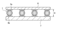
- FIG. 3 shows an example of another mounting structure using a plurality of multilayer metal balls 1.
- the multi-layer metal ball 1 is used in such a manner that a semiconductor element 9 (FIG. 2) having a bump connection structure is necessarily arranged in the gap 8 between the circuit board 7 and the semiconductor element 6 facing each other.
- a semiconductor element 9 FIG. 2
- the multilayer metal ball 1 of the present invention is made of solder by forming the intermediate plating layer 3 sandwiched between the outer layer 4 and the core ball 2 which are solders with Ni or a Ni alloy containing Ni as a main component. Even if the core ball 2 is deformed or melted, a high effect of stabilizing the stacking interval 8 can be obtained.
- the intermediate plating layer 3 made of Ni or Ni alloy is harder than solder, and is formed thicker on the surface of the core ball 2 to suppress deformation of the ball shape even when the core ball 2 is softened.
- the barrier function can be enhanced.
- the intermediate plating layer 3 is a ball mounting step in which the multi-layer metal ball 1 is bonded to the electrode 5b of the substrate 7, and the substrate / electrode in which the electrode 5c of the semiconductor element 6 is bonded to the multi-layer metal ball 1 on the substrate 7. Deformation of the multilayer metal ball 1 can be suppressed during the element mounting process.
- the intermediate plating layer 3 has a higher melting point than the core ball 2 and the outer layer 4, so that it plays a role of deformation resistance against external force without melting. Therefore, it is effective for stabilizing the stacking interval 8 of the semiconductor element 6 and the substrate 7.
- the intermediate plating layer 3 made of Ni or Ni alloy can suppress the reaction at the interface between the core ball 2 made of Sn or Sn alloy and the outer layer 4, and this point is also effective for stabilizing the stacking interval 8. It is.
- the core ball 2 By using Sn or Sn alloy for the core ball 2, it becomes easy to form the core ball 2 having good sphericity and smoothness, and even the multi-layer metal ball 1 having the core ball 2 inside is true sphere. And smoothness are improved.
- the intermediate plating layer 3 Even if the core ball 2 is softened by heating, the intermediate plating layer 3 maintains the good sphericity and smoothness, and isotropically deforms by dispersing the load. There is expected.
- the outer layer 4 made of Sn or an Sn alloy formed on the surface of the intermediate plating layer 3 is selected by selecting the thickness so that the multilayer metal ball 1 does not move on the electrodes 5b and 5c, A sufficient effect of fixing to the substrate 7 can be obtained.
- the intermediate plating layer 3 made of Ni or Ni alloy that is harder than the core ball 2 the core ball 2 made of Sn or Sn alloy, and the outer layer 4 made of Sn or Sn alloy, It was found that the life in the thermal cycle test can be improved by using a structure sandwiched between the two.
- the features and roles of each layer of the multilayer metal ball 1 will be described specifically.
- the core ball 2 Since the Sn or Sn alloy that is the material of the core ball 2 melts at a lower temperature than Cu, the core ball 2 is easier to manufacture than the conventional Cu core ball, and control of the ball shape, ball size, etc. is also possible. Stabilize. Specifically, (i) Sphericality is improved by suppressing ellipse, flatness, etc. during the production of the core ball 2, (ii) The ball surface of the core ball 2 is easy to form smoothly, (iii) The size of the core ball 2 such as (iV) sphericity and smoothness of the surface can be easily changed while keeping the size variation of the core ball 2 at a desired ball diameter low. Is stable. Here, it was confirmed that when a core ball formed of a material other than Sn or Sn alloy solder was used, an elliptical ball was generated or the size stability was lowered.
- Sn has a purity of 99.9% or more and the remainder contains inevitable impurities. Further, it is desirable that the Sn alloy contains Sn as a main component and contains at least 0.02% by mass of any one or more of Ag, Cu, Ni, Zn, Bi, and In. “Sn as a main component” means that the Sn concentration is more than 50% by mass.
- Conventional Sn-Pb alloys can be used as Sn alloys, but Pb-free Sn-Ag alloys, Sn-Cu alloys, Sn-Ag-Cu alloys, Sn- A Zn alloy, Sn—Bi alloy, Sn—In alloy or the like is preferable.
- the core ball 2 contains at least 0.02% by mass of at least one of Ag, Cu, Ni, Bi, Zn, and In, thereby increasing the hardness of the core ball 2 and suppressing deterioration with the passage of time, thereby improving bonding reliability. be able to.
- the Sn-Ag alloy preferably contains 0.5 to 4% by mass of Ag, and may contain 0.02 to 2% by mass of Ni as necessary.
- the Sn-Ag-Cu alloy preferably contains 0.5 to 4% by mass of Ag and 0.1 to 3% by mass of Cu, and may contain 0.02 to 2% by mass of Ni as necessary.
- the Sn—Zn alloy may contain 1 to 5 mass% of Zn, and may contain 0.05 to 10 mass% of Bi and 0.5 to 10 mass% of In as necessary.
- Sn—Zn alloys have the advantages of low melting point and low cost.
- Sn—Bi alloys and Sn—In alloys preferably contain 0.05 to 10% by mass of Bi and 0.5 to 10% by mass of In, have a low melting point, and have good bondability.
- Sn alloys include Sn-Ag-Bi alloys containing 0.5 to 4 mass% Ag and 0.05 to 10 mass% Bi, and Sn-Ag-Bi-In alloys containing 0.5 to 10 mass% In. Sn alloys can also be used.
- Sn-Ag alloy, Sn-Ag-Cu alloy, Sn-Zn alloy, Sn-Bi alloy, Sn-Ag-Bi alloy, Sn-Ag-Bi-In alloy It is desirable that the balance is Sn or the balance is Sn and inevitable impurities.
- the Sn-Ag-Cu alloy ternary solder ball widely used in BGA (Ball Grid Allay) is used as the core ball 2, there is no need to redefine the manufacturing conditions, improving mass productivity. can do.
- the hardness of the core ball 2 can be adjusted by optimizing the components, alloying, and structure.
- Sn which is a candidate for the low melting point metal used for the core ball 2
- Sn is soft and can be further softened by utilizing a reduction in the amount of impurities.
- Concentration measurements in the present invention are measured by EPMA method (Electron Probe Micro Analyzer), EDS method (Energy Dispersive X-ray Spectroscopy) or Auger spectroscopy at five or more random positions in the core ball 2 in the cross section It is desirable to use the average value of. Such measurement of the concentration is the same for the intermediate plating layer 3 and the outer layer 4 described later.
- the diameter of the core ball 2 be 60 ⁇ m or more and 500 ⁇ m or less, and within this range, a stable and good core ball 2 can be obtained. Further, if the diameter of the core ball 2 is more preferably 80 ⁇ m or more, the distribution of variation becomes smaller and classification can be facilitated, so that productivity can be improved.
- the diameter of the core ball 2 is preferably an average value of the diameters of the core balls 2 in the plurality of multilayer metal balls 1.
- the diameter of the core ball 2 is measured by using a photograph taken by SEM (Scanning ⁇ Electron Microscope) observation of the cross section passing through the center of the multi-layer metal ball 1, and a straight line (diameter) passing through the center of the multi-layer metal ball 1 is used.
- the area of the core ball 2 on the diameter may be determined, and this may be used as the diameter of the core ball 2. This utilizes the fact that the boundary between the intermediate plating layer 3 and the core ball 2 can be easily identified by SEM observation.
- the core ball 2 has a diameter of 10 or more multi-layer metal balls 1, and the diameter of the core ball 2 in each multi-layer metal ball 1 is measured. It is desirable to use the average value.
- a procedure for determining a straight line (diameter) passing through the center of the multi-layer metal ball 1 for example, while observing an observation image obtained by SEM of a cross section of the multi-layer metal ball 1, two parallel straight lines can be formed.
- the diameter of the core ball 2 may be measured based on the straight line connecting the contact points on the circumference of the ball 1 as the diameter of the multilayer metal ball 1.
- ⁇ Voids may be included in the core ball 2.
- a cross section passing through the center of the multilayer metal ball 1 is observed with an optical microscope, sufficient bonding reliability can be obtained if the diameter of the void approximate to the sphere is 1/2 or less of the diameter of the core ball 2.
- the intermediate plating layer 3 formed on the surface of the core ball 2 made of Sn or Sn alloy is preferably made of Ni or Ni alloy, and is mainly composed of Ni. “Mainly comprising Ni” means that the Ni concentration exceeds 50 mass%. If the intermediate plating layer 3 is formed of Ni, the intermediate plating layer 3 formed on the surface of the core ball 2 can be easily densified with a substantially uniform thickness.
- the Ni forming the intermediate plating layer 3 is preferably pure Ni (purity 99.9% or more). Pure Ni has a low plating solution and is relatively easy to control the plating process. For Ni alloys, Ni-P alloys and Ni-B alloys are highly effective in making the thickness of the intermediate plating layer 3 uniform. Is obtained.
- the Ni-P alloy preferably contains 1 to 15% by mass of P. Within this range, in addition to stabilizing the size of the multilayer metal ball 1, it is advantageous for suppressing deformation due to hardening. . More preferably, P is in the range of 4 to 13% by mass, and within this range, the sphericity of the multi-layered metal ball 1 becomes higher and the size variation can be further reduced. As a more specific Ni—P-based alloy, an alloy containing P in the above range and the balance being Ni or the balance being made of Ni and inevitable impurities is desirable.
- the plating solution to be used can be classified according to pH, and an acidic bath (pH 4 to 6), a neutral bath (pH 6 to 8), and an alkaline bath (pH 8 to 11) can be used.
- An acidic bath is stable in the liquid state of the bath and easy to use.
- Ni-B alloy it is desirable to contain 0.1 to 6% by mass of B. Within this range, the effect of smoothing the surface of the intermediate plating layer 3 is enhanced, and the sphericity of the multilayer metal ball 1 is increased. It becomes good.
- an alloy containing B in the above range, the balance being Ni, or the balance being composed of Ni and inevitable impurities is desirable.
- the Ni-P-B alloy contains 1 to 15% by mass of P and 0.1 to 6% by mass of B. More specifically, for example, a Ni-PB alloy includes 1 to 15% by mass of P and 0.1 to 6% by mass of B, with the balance being Ni or the balance being Ni and inevitable impurities. It is desirable.
- the B concentration (P concentration) in the intermediate plating layer 3 described above is a relative ratio of the B concentration (P concentration) to the Ni concentration.
- ICP Inductively-Coupled-Plasma
- the concentration of Ni, B, P occupying the entire multi-layer metal ball 1 is measured, and B concentration / Ni concentration.
- the B concentration and the P concentration, which are relative ratios, are obtained from the P concentration / Ni concentration, and are used as the B concentration and the P concentration of the intermediate plating layer 3, respectively.
- B and P which are light elements, are difficult to detect by the atomic absorption method. That is, it is difficult to measure the B concentration and the P concentration inside the intermediate plating layer 3 by using normal chemical analysis such as EPMA method and EDS method. Therefore, as described above, the overall B concentration, P concentration, and Ni concentration of the multilayer metal ball 1 are obtained by ICP analysis, and the relative ratio of the B concentration to the Ni concentration in the entire multilayer metal ball 1 is determined by intermediate plating.
- the B concentration of the layer 3 is defined, and the relative ratio of the P concentration to the Ni concentration in the multilayer metal ball 1 as a whole is preferably defined as the P concentration of the intermediate plating layer 3.
- each layer is selectively dissolved by utilizing the difference in melting point of each layer and the ease of acid dissolution.
- ICP analysis can also be performed. For example, by dissolving only the outer layer 4 using acid dissolution, a melting point difference, etc., separating only the outer layer 4 from the surface of the intermediate plating layer 3, and performing ICP analysis on the separated outer layer 4, the outer layer 4 The presence or absence of B and P can be confirmed.
- the outer layer 4 is removed, and a two-layered ball composed of the intermediate plating layer 3 and the core ball 2 is embedded and polished in a resin or the like so that the core ball 2 is exposed, and acid dissolution, melting point difference, etc.
- a two-layered ball composed of the intermediate plating layer 3 and the core ball 2 is embedded and polished in a resin or the like so that the core ball 2 is exposed, and acid dissolution, melting point difference, etc.
- the core ball 2 that is a core material is used.
- the concentrations of B, P, and Ni in the outer layer 4 are also summed.
- the core ball 2 and the outer layer 4 include B and P.
- the solid solution amounts of B and P in Sn are almost zero, and the solid solution amount of Ni is also small.
- the entire B concentration, P concentration, and Ni concentration of the multilayer metal ball 1 are B, P, and Ni caused by the intermediate plating layer 3.
- the core ball 2 and / or the outer layer 4 is formed of a Sn alloy, even if B, P, and Ni are included in the Sn alloy, the amount of B, P, and Ni is small. Regulating the relative ratio of B concentration to Ni concentration and the relative proportion of P concentration to Ni concentration as the B concentration and P concentration of intermediate plating layer 3, and defining the range of B concentration and P concentration in intermediate plating layer 3 However, it does not affect the operational effects of the above numerical limitation in the intermediate plating layer.
- the thickness of the intermediate plating layer 3 is desirably 3 ⁇ m or more and 100 ⁇ m or less. When the thickness is within this range, compression deformation during mounting can be suppressed, the size of the core ball 2 can be stabilized by the intermediate plating layer 3, and the stacking interval 8 can be maintained. If the thickness of the intermediate plating layer 3 is less than 3 ⁇ m, the effect of reducing the deformation is reduced. On the other hand, if the thickness of the intermediate plating layer 3 is greater than 100 ⁇ m, the thickness of the intermediate plating layer 3 is made uniform. It becomes difficult to form, the sphericity is lowered, and stabilization of the stacking interval 8 becomes difficult.
- the lower limit of the thickness of the intermediate plating layer 3 is more preferably 5 ⁇ m or more. In this case, the effect of stabilizing the stacking interval 8 after mounting can be obtained, and more preferably 10 ⁇ m or more. A higher effect of suppressing the deformation of the multilayer metal ball 1 can be obtained.
- the upper limit of the thickness of the intermediate plating layer 3 is more preferably 50 ⁇ m or less. In this case, the thickness of the intermediate plating layer 3 can be made more uniform, and variations in ball diameter can be further suppressed. .
- a straight line (diameter) passing through the center of the multilayer metal ball 1 is determined using a photograph taken by SEM observation of a cross section passing through the center of the multilayer metal ball 1,
- the thickness of the intermediate plating layer 3 on the diameter may be measured. This utilizes the fact that the boundary between the intermediate plating layer 3 and the outer layer 4 and the boundary between the intermediate plating layer 3 and the core ball 2 can be easily identified by SEM observation.
- the intermediate plating layer 3 may be defined as a region where the concentration of Ni is 50 mass% or more. That is, the boundary of the intermediate plating layer 3 may be 50% by mass of Ni on both the core ball 2 side and the outer layer 4 side.
- the thickness of the intermediate plating layer 3 is preferably an average value obtained by preparing a plurality of multilayer metal balls 1 and determining the thickness of the intermediate plating layer 3 from each of the multilayer metal balls 1. In order to confirm the variation in the thickness of the intermediate plating layer 3, the thickness of the intermediate plating layer 3 should be 10 or more. It is desirable to measure the thickness and use the average value.
- a procedure for determining a straight line (diameter) passing through the center of the multilayer metal ball 1 as in the procedure described above, while viewing the observation image obtained by SEM of the cross section of the multilayer metal ball 1, Two parallel straight lines may be aligned with the contact points on the circumference of the multilayer metal ball 1, the distance between the parallel straight lines may be measured, and the measurement result (the distance between the parallel straight lines) may be used as the diameter of the multilayer metal ball 1.
- the outer layer 4 does not directly affect the stacking interval 8 because the Sn of the outer layer 4 is melted and bonded. It is the combination of the intermediate plating layer 3 and the core ball 2 that maintains the lamination interval 8 when the outer layer 4 is melted, and it is considered that the load resistance in this combination is effective.
- the multilayer metal ball 1 on which the outer layer 4 is formed is used. It is difficult to evaluate.
- a ball compression test using “a two-layered ball of intermediate plating layer 3 and core ball 2 (intermediate product)” in which the outer layer 4 is not formed It is also effective to evaluate with
- a “ball having a two-layer structure of an intermediate plating layer 3 and a core ball 2” in which the outer layer 4 is not formed is used as a ball compression test. Evaluation was performed.
- the intermediate plating layer 3 desirably has a Vickers hardness of 150 Hv or more and 1000 Hv or less. If the Vickers hardness is 150 Hv or more, the effect of maintaining the shape against local pressurization can be obtained by forming the intermediate plating layer 3 made of Ni or Ni alloy thick. Further, the Vickers hardness is more preferably 300 Hv or more, in this case, the effect of suppressing deformation of the intermediate plating layer 3 during heating is high, and more preferably 500 Hv or more, in this case The effect of suppressing deformation in the above-described ball compression test is further increased. If the upper limit of the Vickers hardness in the intermediate plating layer 3 is 1000 Hv or less, the occurrence of cracks in the intermediate plating layer 3 can be suppressed.
- the intermediate plating layer 3 made of Ni or Ni alloy can have various hardnesses depending on the manufacturing method of the intermediate plating layer 3 and the elements added to the intermediate plating layer 3. For example, when the intermediate plating layer 3 is formed by electroplating, an intermediate plating layer 3 having a Vickers hardness of 150 Hv or more can be obtained. When the intermediate plating layer 3 is formed by electroless plating, Vickers An intermediate plating layer 3 having a hardness of 500 Hv or more can be obtained. Furthermore, when the intermediate plating layer 3 is formed by electroless Ni plating treatment in which B is added to Ni, the intermediate plating layer 3 having a Vickers hardness of 700 Hv or more can be obtained.
- the intermediate plating layer 3 When the intermediate plating layer 3 is formed by electroless Ni plating treatment in which P is added to Ni, the intermediate plating layer 3 having a Vickers hardness of 700 Hv or more can be obtained by heat treatment at 400 ° C. or higher.
- the multilayer metal ball 1 can be obtained by forming the intermediate plating layer 3 having a high Vickers hardness on the surface of the core ball 2, whereby the multilayer metal ball 1 having excellent load resistance can be obtained.
- Ni forming the intermediate plating layer 3 is hard, and it is relatively easy to increase the hardness by alloying, selecting a plating solution, or the like.
- the ratio of the intermediate plating layer 3 covering the core ball 2 it is preferable to cover the entire core ball 2.
- a part of the intermediate plating layer 3 may include a crack or a defect. If the cross section passing through the center of the multi-layered metal ball 1 is observed with an optical microscope and the intermediate plating layer 3 covers 70% or more of the outer peripheral length of the core ball 2, it is possible to ensure bonding reliability. is there. Preferably, if 80% or more of the outer peripheral length is covered, the quality is stabilized and it becomes easy to ensure the bonding reliability.
- the void may be included in the intermediate plating layer 3.
- the void may be included in the intermediate plating layer 3.
- the outer layer 4 is made of Sn or an Sn alloy, and the purity of Sn is preferably 99.9% or more, and the balance may contain inevitable impurities. Further, it is desirable that the Sn alloy contains Sn as a main component and contains at least 0.05% by mass of any one or more of Ag, Cu, Ni, Zn, Bi, and In. “Sn as a main component” means that the Sn concentration is more than 50% by mass. Sn has a low melting point of 231 ° C., has good adhesion to Ni or Ni alloy forming the intermediate plating layer 3, and has bonding properties to the semiconductor element 6 and the electrodes 5b and 5c of the substrate 7. Is also good.
- Sn-Pb alloys can also be used as Sn alloys, but Pb-free Sn-Ag alloys, Sn-Cu alloys, Sn-Ag-Cu alloys, Sn-based materials that emphasize environmental friendliness -Zn alloys, Sn-Bi alloys, Sn-In alloys, etc. are advantageous.
- the Sn alloy preferably contains at least one of Ag of 0.1 to 4 mass%, Cu of 0.1 to 2 mass%, and Ni of 0.05 to 1 mass%. In this case, the hardness of the outer layer 4 is increased, There are advantages such as improved bonding reliability with respect to impact characteristics and the like.
- the above-described Sn-Ag alloy preferably contains 0.1 to 4% by mass of Ag.
- the balance may be Sn, or the balance may be composed of Sn and inevitable impurities.
- the Sn-Ag-Cu alloy preferably contains 0.1 to 4% by mass of Ag, 0.1 to 2% by mass of Cu, and 0.05 to 1% by mass of Ni.
- the balance is Sn or the balance is Sn. It is good also as a structure which consists of an unavoidable impurity.
- the Sn—Zn alloy may contain 3 to 10% by mass of Zn, and 0.05 to 10% by mass of Bi if necessary.
- the Sn—Zn-based alloy may be configured such that the balance at this time is Sn or Sn and inevitable impurities.
- the Sn—Zn-based alloy has advantages such as a low melting point and low cost.
- the Sn—Bi alloy preferably contains 0.05 to 10% by mass of Bi.
- the balance may be Sn or the balance may be composed of Sn and inevitable impurities.
- the Sn—Bi system has a low melting point and good bondability with the multilayer metal ball 1.
- Sn-Ag-Bi system can also be used. In the Sn-Ag-Bi system, it is preferable to contain 0.1 to 4% by mass of Ag and 0.05 to 10% by mass of Bi, and may contain In as necessary. At this time, the remaining portion may be Sn, or the remaining portion may be composed of Sn and inevitable impurities.
- addition of 0.5 to 10% by mass of In improves reliability in addition to lowering the melting point.
- the hardness of the outer layer 4 can be adjusted by optimizing the components, alloying, and structure.
- Sn which is a candidate for the low melting point metal used in the outer layer 4
- the outer layer 4 is formed by diverting Sn-Ag-Cu ternary solder balls widely used in BGA (Ball Grid Allay), mass productivity is improved and reflow in use Since generally used conditions can be used, the thermal effect on other mounted parts can be reduced.
- the outer layer 4 is preferably formed to have a thickness of 2 ⁇ m or more and 50 ⁇ m or less. By making the thickness within this range, the movement of the multilayer metal ball 1 due to melting of the outer layer 4 can be suppressed during the thermal cycle test. Thus, the effect of stabilizing the stacking interval 8 is increased, and the bonding reliability such as the bonding strength can be improved. If the thickness of the outer layer 4 is less than 2 ⁇ m, the bonding reliability in the thermal cycle test is lowered, which is not preferable.
- the thickness of the outer layer 4 is more than 50 ⁇ m, the multilayer metal ball 1 may move due to melting of the outer layer 4 during reflow and protrude from the electrodes 5b and 5c, which is not preferable because the stacking interval 8 becomes unstable.
- the thickness of the outer layer 4 is desirably in the range of 2 ⁇ m or more and 30 ⁇ m or less, and within this range, the bonding reliability during the thermal cycle test is further improved.
- Voids may be included in the outer layer 4.
- the diameter of the void approximate to the sphere is 1/2 or less of the thickness of the outer layer 4, sufficient bonding reliability can be obtained.
- a diffusion layer or an intermetallic compound layer may be formed at the interface of the core ball 2 / intermediate plating layer 3 or the interface of the intermediate plating layer 3 / outer layer 4.
- the intermetallic compound layer can be formed by interdiffusion at the interface or by melt alloying.
- the thickness of the intermetallic compound layer is in the range of 0.1 to 10 ⁇ m, the adhesion is improved and the smoothness of the interface is improved.
- the thickness of the intermetallic compound layer of the multilayer metal ball 1 means that the thickness of the intermetallic compound layer of the multilayer metal ball 1 is prepared from each multilayer metal ball 1 by preparing a plurality of multilayer metal balls 1.
- the average value of the thicknesses of the intermetallic compound layers in the plurality of multi-layer metal balls 1 is desirable.
- the thickness of the intermetallic compound layer the thickness of the intermetallic compound layer at an arbitrary location is observed while viewing the observation image obtained by SEM of the cross section of each multi-layered metal ball 1 in the same manner as described above. The thickness can be measured visually or by image analysis, and the average value of the plurality of measurement results can be used as the thickness of the intermetallic compound layer.
- the wire cut method is a method of producing a ball of a predetermined size by manufacturing a thin wire, then cutting it into a predetermined length, melting and solidifying it, and is advantageous for stabilizing the size.
- the droplet method is a method of forming a ball by heating and melting a Sn or Ni alloy having a low melting point to form a droplet.
- the droplet method is characterized by high ball productivity by adjusting the amount and concentration of the droplets.
- the production of the core ball 2 is not limited to the production method described above, and may be produced by various production methods.
- the intermediate plating layer 3 on the core ball 2 it can be formed by performing electroless plating treatment or electrolytic plating treatment with a normal barrel apparatus using a commercially available plating solution.
- Plating materials are classified into pure Ni, Ni-P system, and Ni-B system, and commercial plating solutions were used for all.
- the intermediate plating layer 3 was formed at room temperature using a normal watt bath.
- the electroless plating process is advantageous for making the thickness of the intermediate plating layer 3 uniform.
- the film forming speed is fast, which is advantageous for productivity.
- An appropriate plating method may be selected depending on the components, the plating solution, the thickness of the intermediate plating layer 3 to be formed, and the like. In consideration of productivity, manufacturing cost, etc., it is desirable to form the intermediate plating layer 3 by a normal barrel apparatus using a commercially available plating solution.
- the electroless plating treatment is advantageous for obtaining a uniform film thickness and composition.
- the intermediate plating layer 3 made of Ni-P As an alloy-based plating treatment, for example, in order to make the P content in the intermediate plating layer 3 made of Ni-P be 6 to 15% by mass, an electroless plating bath composition and plating conditions are appropriately selected. It ’s fine.
- the intermediate plating layer 3 can be formed using a commercially available plating solution in which nickel salt, hypophosphite, or the like is mixed.
- the outer layer 4 made of Sn or Sn alloy may be formed by either electrolytic plating or electroless plating, but the electrolytic plating is simple.
- the composition of the electrolytic plating solution may be a sulfuric Sn plating solution using stannous sulfate.
- the plating apparatus is not particularly limited as long as it is a barrel plating apparatus.
- the outer layer 4 can be formed by plating the surface of the intermediate plating layer 3 at room temperature.
- the Sn alloy of the outer layer 4 for example, when the outer layer 4 made of a Sn—Ag alloy is formed by plating, a commercial product of an alkanol sulfonic acid plating solution can be used.
- a plating solution used when forming the outer layer 4 made of a Sn—Ag—Cu alloy by plating a solution containing sulfonic acids and Sn, Ag and Cu as essential components as metal components can be used.
- a desired plating solution can be obtained by mixing a plating mother solution made of sulfonic acids with a metal compound, and an organic complexing agent can be contained for the stability of metal ions.
- electrolytic plating is advantageous for productivity.
- the multilayer metal ball 1 is constituted by the core ball 2 made of Sn or Sn alloy, the intermediate plating layer 3 made of Ni or Ni alloy, and the outer layer 4 made of Sn or Sn alloy,
- the thickness of the plating layer 3 was 3 ⁇ m or more and 100 ⁇ m or less.
- the core ball 2 is formed of Sn or Sn alloy, and the intermediate plating layer 3 is selected to have an optimum thickness. It can be formed and high bonding reliability can be realized.
- the intermediate plating layer 3 formed thick on the surface of the core ball 2 can suppress the ball deformation at the time of load application or heating in the reflow process, and can realize a stable spacer function. Therefore, it is possible to provide the multi-layered metal ball 1 having an excellent spacer function and high bonding reliability.
- the core ball 2 made of Sn or Sn alloy, which has a lower melting point than Cu, is used to produce a special production that was necessary when producing a conventional Cu core ball.
- An apparatus becomes unnecessary, and the manufacturing cost and the labor at the time of manufacture can be reduced correspondingly.
- an electroless plating process or an electrolytic plating process was performed with a normal barrel apparatus using a commercially available plating solution.
- the plating materials were pure Ni, Ni-P, and Ni-B, and commercially available plating solutions were used for all.
- pure Ni plating it was performed at room temperature using a normal watt bath.
- Ni-P system plating was performed at 70 ° C. using a Ni-P electroless plating solution containing hypophosphite and the like.
- plating was performed at 60 ° C. using a Ni-B system electroless plating solution containing a borohydride compound.
- the surface of the ball on which the intermediate plating layer was formed was plated with solder containing Sn to form an outer layer.
- solder containing Sn solder containing Sn to form an outer layer.
- a solution containing Sn salt or the like was used as an electrolytic plating treatment at room temperature.
- an outer layer of a Sn alloy containing Ag, Cu, etc. in the Sn system was formed by plating to produce a multilayer metal ball with improved hardness and adhesion.
- the multi-layer metal ball was polished to obtain a cross section passing through the center of the multi-layer metal ball, and the cross section was observed with an SEM to measure the diameter of the core ball, the thickness of the intermediate plating layer, and the thickness of the outer layer. . Or partly measured thickness from line analysis by EPMA or AES.
- the alloy concentrations of the core ball, the intermediate plating layer, and the outer layer were measured by the average value of five or more EPMA point analyses.
- the B concentration and P concentration in the intermediate plating layer were determined by the relative ratio of the B concentration to the Ni concentration in the entire multilayer metal ball. Specifically, the concentration of Ni, B, and P in the entire multilayer metal ball is measured by dissolving the multilayer metal ball with an acid and performing ICP analysis. The B concentration as a relative ratio was calculated, and the P concentration as a relative ratio was calculated from the P concentration / Ni concentration.
- the diameter of the multilayer metal ball was taken as the diameter of the multilayer metal ball.
- the diameter of the core ball, the thickness of the intermediate plating layer, and the thickness of the outer layer were measured using image analysis software for the thickness on the straight line (diameter) passing through the center of the multilayer metal ball.
- the diameter of the core ball in 10 multilayer metal balls was obtained from the diameter of the core ball, the thickness of the intermediate plating layer, and the thickness of the outer layer obtained from the 10 multilayer metal balls having the same composition.
- the average value (core ball diameter), the average value of the thickness of the intermediate plating layer, and the average value of the thickness of the outer layer were examined.
- the Vickers hardness was measured for the intermediate plating layer of the multilayer metal ball.
- a multi-layer metal ball is polished to obtain a cross-section passing through the center of the multi-layer metal ball, which is approximately the center of the cross-section of the intermediate plating layer, and approximately the center of the thickness of the intermediate plating layer The hardness was measured on the part.
- the thickness of the intermediate plating layer was less than 25 ⁇ m
- the thickness of the intermediate plating layer formed by plating with the same component to a thickness of 25 ⁇ m was separately prepared and measured. The results are shown in Table 1.
- the Vickers hardness of the intermediate plating layer means that five multi-layer metal balls are prepared for each of Examples 1 to 17 and Comparative Examples 1 to 8 in Table 1. Vickers hardness was measured 5 points at a time and the average value was examined.
- each electrode of a semiconductor element and a resin substrate (also simply referred to as a substrate) was connected to prepare a mounting sample on which the multi-layer metal ball was mounted.
- a silicon chip was used as the semiconductor element, and the size was 30 ⁇ 30 mm.
- As the resin substrate a commercially available glass epoxy substrate was used, and the size was 40 ⁇ 40 mm.
- an electrode having a structure of Al film 0.8 ⁇ m, Ni film 0.2 ⁇ m, and Au film 0.01 ⁇ m was formed on the back surface of the semiconductor element.
- the electrode on the surface of the resin substrate had a structure of Cu film 0.5 ⁇ m, Ni film 0.2 ⁇ m, and Au film 0.02 ⁇ m.
- the number of electrodes was 10 per side, arranged on four sides, for a total of 40.
- a multi-layer metal ball was arranged at the electrode position using a general-purpose ball mounter. At this time, a water-soluble flux was applied on the electrode in advance, the multi-layer metal ball was aligned with the electrode position, and then installed with a light load of 5 to 50 gf per multi-layer metal ball. .
- the multilayer metal ball and the resin substrate electrode were joined at room temperature.
- a flip chip bonder was used to align the electrodes of the semiconductor element and the multi-layer metal balls, and temporarily joined them. At this time, by preliminarily applying a flux to the electrodes on the semiconductor element, the temporary bonding works well.
- the above connected sample was passed through a reflow process, and the bonding strength between the multilayer metal ball and the electrode was ensured by melting the outer layer.
- the preheating was performed in the range of 130 to 200 ° C. for 1 to 3 minutes, and then heated at the maximum temperature range of 230 to 300 ° C. for 0.5 to 1.5 minutes.
- the atmosphere was N2 flow.
- TCT thermal cycle test
- Table 1 shows the results of examining the composition of the core ball, the intermediate plating layer, and the outer layer of the multilayer metal balls of Examples 1 to 17 and Comparative Examples 1 to 8.
- Table 1 also shows the diameter of the core ball, the thickness of the intermediate plating layer, the thickness of the outer layer, and the intermediate plating obtained from a plurality of multilayer metal balls for each of Examples 1 to 17 and Comparative Examples 1 to 8.
- the results of examining the Vickers hardness of the layer and the diameter (overall diameter) of the multilayer metal ball are shown.
- Table 1 investigates the interval maintenance after stacking in the mounting sample, the variation in the size of the multilayer metal balls, and the stacking interval after TCT for each of Examples 1 to 17 and Comparative Examples 1 to 8. The results are shown.
- Table 1 shows that a ball compression test was carried out on a ball having a two-layer structure of an intermediate plating layer and a core ball produced for each of Examples 1 to 17 and Comparative Examples 1 to 8, and compression deformation was performed. The result of having investigated about ability is shown.
- the average value of the amount of deformation with respect to the ball diameter of the two-layered ball before the ball compression test was evaluated as “compression deformability”.
- 10 double-layer balls were prepared for each of Examples 1 to 17 and Comparative Examples 1 to 8, and a ball compression test was performed on these two-layer balls and a load of 200 gf was applied. The average value of the deformation amount was measured.
- compression deformability was examined under four types of conditions for a single-layered ball consisting of an intermediate plating layer and a core ball. Specifically, when the reflow treatment is performed once for a two-layer ball, the reflow treatment is performed for a two-layer ball when the reflow treatment is performed twice for a two-layer ball. When subjected to three cycles, the “compression deformability” was examined for four types of balls having a two-layer structure subjected to 100 cycles of TCT treatment. However, the test for performing the reflow treatment three times was performed only for Examples 5, 16, and 17.
- the reflow process is the above-mentioned “reflow process” (in the N2 flow atmosphere, in the range of 130 to 200 ° C for 1 to 3 minutes, after preheating, the maximum temperature of 230 to 300 ° C in the temperature range of 0.5 to 1.5 minutes Heating) was performed under the same conditions.
- the TCT treatment was performed under the same conditions as in the above-mentioned “TCT” (a series of steps of maintaining at ⁇ 40 ° C. for 30 minutes and then maintaining at 125 ° C. for 30 minutes).
- the results of examining the stacking interval for the mounting sample immediately after mounting before performing TCT are shown in the column “Maintaining spacing after stacking (immediately after mounting)” in Table 1, and stacking for the mounting sample that was subjected to 100 cycles of TCT.
- the results of examining the intervals are shown in the column “100 stacking intervals after TCT” in Table 1.
- the spacer function indicates that the average value of the stacking interval is the same as the core ball diameter (core ball diameter) and the stacking interval can be maintained. Judgment is good, if it is within the range of 0.5 to 2 ⁇ m beyond the diameter of the core ball, ⁇ is judged as good, and if it is within the range of more than 2 ⁇ m from the diameter of the core ball, when mounted Since the height of can not be maintained, there is a problem.
- Examples 1 to 17 are composed of a core ball made of Sn or Sn alloy, an intermediate plating layer made of Ni or Ni alloy, and an outer layer made of Sn or Sn alloy, and the thickness of the intermediate plating layer is 3 to
- the multilayer metal ball satisfies all the configurations of 100 ⁇ m.
- the excellent spacing function has been confirmed, such as maintaining the stacking interval immediately after mounting and small variations in the size of the multi-layer metal balls. It was done.
- Comparative Examples 1 to 8 since any of the above-described configurations was not satisfied, it was confirmed that there was a problem in the variation in the stacking interval immediately after mounting or the size of the multilayer metal balls.
- the intermediate plating layer is formed of Ni or a Ni alloy and the thickness of the intermediate plating layer is in the range of 3 to 100 ⁇ m, the variation in ball size is kept low.
- the thickness of the intermediate plating layer was in the range of 5 to 50 ⁇ m, and thus the variation was particularly well suppressed. .
- Examples 1 to 17 since the thickness of the intermediate plating layer is in the range of 3 to 100 ⁇ m, the compressive deformability after one reflow is good, but among them, Examples 1 to 5 and 7 to 17 In addition, since the thickness of the intermediate plating layer is in the range of 5 to 100 ⁇ m, the compression deformability after one reflow was particularly good. In Examples 1 to 5, 7 to 9, and 11 to 17, since the thickness of the intermediate plating layer was in the range of 10 to 100 ⁇ m, good results were obtained even in the compressive deformability after two reflows.
- Examples 1, 3 to 5, 7 to 15, and 17 since the Vickers hardness of the intermediate plating layer is in the range of 150 to 1000 Hv, the evaluation of the compressive deformability after 100 cycles of TCT is “ ⁇ ” or more. It was good. In particular, Examples 1, 3 to 5, 8 to 15 and 17 have a hardness in the range of 300 to 1000 Hv. Therefore, the evaluation of compression deformability after 100 cycles of TCT is “ ⁇ ”, which is better. there were.
- the thickness of the outer layer is in the range of 2 to 50 ⁇ m, so the stacking interval after TCT is good, and it is confirmed that the thermal cycle evaluation after mounting has excellent bonding reliability did it.
- the thickness of the outer layer was in the range of 2 to 30 ⁇ m, so that the stacking interval after TCT was more excellent.
- Examples 5-16 and 17 the reflow treatment was performed three times for “compressive deformability”, but the compressive deformability due to the difference in the composition of the intermediate plating layer was evaluated. In the third reflow, it was confirmed that there was no practical problem. Among them, Examples 5 and 17 were less deformed because the intermediate plating layer had a hardness of 300 Hv or more, and among them, in Example 5, the intermediate plating layer had a hardness of 500 Hv or more, and particularly good results were obtained.
Landscapes
- Chemical & Material Sciences (AREA)
- Engineering & Computer Science (AREA)
- Mechanical Engineering (AREA)
- Materials Engineering (AREA)
- Metallurgy (AREA)
- Organic Chemistry (AREA)
- Electric Connection Of Electric Components To Printed Circuits (AREA)
Abstract
スペーサ機能に優れ、かつ、接合信頼性が高い複層金属ボールを提供する。複層金属ボール1では、コアボール2をSnまたはSn合金で形成し、中間めっき層3を最適な厚さに選定したことにより、真球性が良好な複層金属ボール1を形成でき、高い接合信頼性を実現できる。また、複層金属ボール1では、コアボール2の表面に厚く形成した中間めっき層3によって、荷重負荷時やリフロー工程の加熱時におけるボール変形を抑制し得、安定したスペーサ-機能を実現できる。従って、スペーサ機能に優れ、かつ、接合信頼性が高い複層金属ボール1を提供できる。
Description
本発明は、半導体素子、パッケージ、回路基板などを積層させて接続するときに用いる複層金属ボールに関するものである。
携帯電話などモバイル機器の高機能化、小型化に伴い、半導体実装の小型化、薄型化が要求されている。半導体実装に用いられる接続材料には、電気的導通または基板の構造的接続など多くの機能が要求される。接続材料を大別すると、半導体素子の電極と基板とを接続する半導体の内部接続と、その半導体素子を実装した半導体パッケージと回路基板とを接続する半導体の外部接続と、に分けられる。
半導体実装の内部接続には、半導体素子の電極と樹脂基板との接合にボールが用いられることが増えている。従来のワイヤ接続に比べて、ボールを用いた接続(以下、ボール接続とも称す)では高集積化、高周波化に対応する高密度接続に有利である。また、半導体パッケージの外部接続には、小型化、薄型化に適応する面実装に適応するため、最近はボール接続が用いられている。
これらのボールの素材には、通常ははんだが用いられることが多い。リフロー工程によりはんだボールを溶融することで、比較的容易に接合強度を得ることが可能である。電子機器の小型化、高機能化が進むことで、最近では、積層構造、MCM(Multi Chip Module)などの3次元実装が進化している。複数の素子または半導体パッケージを上下方向に積層することで実装面積の縮小に有利である。このような3次元実装では、積層の間隔を制御することが重要である。最近では、積層された素子と基板との上下間隔に、さらに別の素子を組み込んだハイブリッド構造も開発されている。そして、この際、積層の間隔を制御することは、製品の性能、品質を左右することになるため重要となる。
積層された半導体素子、半導体パッケージ(以下、総称して積層部品と称す)の基板への設置、固定には、ボールを用いた接続が使用できる。このような積層部品の基板への設置等に用いるボールに対しては、積層部品を接続する接合強度、および、積層間隔(高さ)を制御するスペーサ機能などが求められる。さらに、このようなボール接続では、積層された電極間をボールバンプで電気的に接続する場合もある。従来では、この種のボールとしては、はんだボール、あるいは表面にはんだを被覆したCuコアボールを用いることができる(例えば、特許文献1および特許文献2参照)。
はんだボールは、溶融により接合は容易であるため接合用には適しているが、融点が低いため、ボール接合時に変形し易い。そのため、はんだボールは、積層部品間、あるいは、積層部品と基板との間等の間隔(以下、積層間隔と称す)を調整することが難しく、スペーサ機能は劣るという問題があった。積層部品を安定して組み立てるためには、この積層間隔を所定のサイズで精度良く維持することが重要なポイントとなる。この点、Cuをコアボールとする複層金属ボールでは、融点が高く変形しにくいCuをコアボールとしているため、スペーサ機能に優れ、積層間隔の調整は可能である。しかしながら、Cuコアボールは、高温で溶融する等の理由から、サイズの整った真球性の良好なコアボールの製造は難しい。そのため、Cuをコアボールとして用いた複層金属ボールでは、半導体素子および基板間の間隔制御のためにスペーサとして使用すると、複層金属ボールの真球性の低下によって、接合時の配列位置での安定性が低下して接合不良が生じ易くなる等、接合信頼性が低下してしまう恐れもあった。
そこで、本発明は、スペーサ機能に優れ、かつ、接合信頼性が高い複層金属ボールを得ることを目的とする。
本発明による複層金属ボールは、SnまたはSn合金からなるコアボールと、NiまたはNi合金からなり、前記コアボールを覆う中間めっき層と、SnまたはSn合金からなり、前記中間めっき層を覆う外層と、により構成されており、前記中間めっき層の厚さが3μm以上100μm以下であることを特徴とする。
本発明では、コアボールをSnまたはSn合金で形成し、中間めっき層を最適な厚さに選定したことにより、真球性が良好な複層金属ボールを形成でき、高い接合信頼性を実現できる。また、本発明では、コアボールの表面に厚く形成した中間めっき層によって、荷重負荷時やリフロー工程の加熱時におけるボール変形を抑制し得、安定したスペーサ-機能を実現できる。従って、スペーサ機能に優れ、かつ、接合信頼性が高い複層金属ボールを提供できる。
以下、図面を参照して本発明の実施の形態について詳細に説明する。
(本発明の複層金属ボールの概略)
ボール接続においては、積層間隔を制御するスペース機能を向上し、積層部品の十分な接合強度が得られ、実装後の接合信頼性を向上できるボール材料が求められる。そこで、本発明者らは、コアボールの素材としてSnまたはSn合金である球状のはんだを用いて、高いスペーサ機能を有する複層金属ボールの開発に取り組んだ。
ボール接続においては、積層間隔を制御するスペース機能を向上し、積層部品の十分な接合強度が得られ、実装後の接合信頼性を向上できるボール材料が求められる。そこで、本発明者らは、コアボールの素材としてSnまたはSn合金である球状のはんだを用いて、高いスペーサ機能を有する複層金属ボールの開発に取り組んだ。
SnまたはSn合金からなるコアボールを用いる利点としては、形状をボール状に形成する製造工程が簡単であること、ボールサイズを容易に変えられ、さらにボールサイズを高精度に制御できること、真球性、表面の平滑性などの形状が安定化すること、が挙げられる。従来のCuコアボールでは、Cuがはんだよりも高融点であることから、高温で溶融する特殊な溶解装置が必要となり、ボールのサイズばらつきが生じ易く、また、楕円や扁平のボールが形成される場合もあるなどの問題があった。
複層金属ボールのコアボールをSnまたはSn合金で製造したときには、ボール接合時に行われるリフロー工程において、コアボールが溶融してしまうことから、積層する基板等の重さや、負荷荷重に耐えられるようにし、複層金属ボールが潰れずに本来確保すべき基板や素子の積層間隔を維持させることが重要であり、また、部品同士の接触や電極の接触に不良が生じることを防止する必要もある。
本発明者らが、上記問題を解決するためにスペース機能を高める複層金属ボールを鋭意検討した結果、複層金属ボールのコアボールをSnまたはSn合金で形成し、当該コアボール表面に、NiまたはNi合金からなる中間めっき層を厚く形成し、さらに、当該中間めっき層表面にSnまたはSn合金からなる外層を設けた3層構造とすることが有効であることを見出した。さらに、コアボール、中間めっき層の組成や、硬さなどの制御が有効であることを見出した。
図1は、本発明による複層金属ボールの断面構造を示す。図1に示すように、複層金属ボール1は、内部から表面方向に向けて、コアボール2、中間めっき層3、外層4の順に設けられた構成を有する。具体的には、外層4およびコアボール2は、SnまたはSn合金からなり、その外層4およびコアボール2の間に、Niを主成分とする中間めっき層3が設けられており、当該中間めっき層3の厚さが厚く形成されている。このような複層金属ボール1であれば、半導体素子や半導体パッケージ品などを積層した部品(積層部品)を接続するときに、半導体素子および基板などの積層間隔を維持するスペーサ機能を高められ、また、接合信頼性をも高められる。
図2には、複数の半導体素子6,9が回路基板(単に、基板とも称す)7上に積層された実装構造の一例を示す。半導体素子9はバンプ10を介して回路基板7の電極5aに接続されている。この実装構造では、半導体素子9よりも高い位置に電子部品としての他の半導体素子6が接続される必要があり、この半導体素子6と回路基板7との接続に複層金属ボール1が用いられている。積層された部品(ここでは、半導体素子6および回路基板7)の間隔8(積層間隔)をある一定の値に保つために、複層金属ボール1には高いスペーサ機能が求められる。図2に示した実装構造では、回路基板7の電極5bと、半導体素子6の電極5cと、に複層金属ボール1が接合されており、これら回路基板7および半導体素子6間に複層金属ボール1によって形成した間隔8の空間内に、バンプ接続構造を有した半導体素子9が配置されている。
図3は、複数の複層金属ボール1を使用した他の実装構造の一例を示す。図3に示すように、複層金属ボール1の使用形態としては、バンプ接続構造を有した半導体素子9(図2)が、対向する回路基板7および半導体素子6間の間隙8に必ずしも配置されている必要はなく、回路基板7および半導体素子6間の間隙8を一定に保つスペーサとして機能させつつ、さらに、回路基板7の電極5bと、半導体素子6の電極5cと、を導通させる目的に用いるものであってもよい。
本発明の複層金属ボール1は、はんだである外層4およびコアボール2に挟まれた中間めっき層3を、Ni、または、Niを主成分としたNi合金により形成することで、はんだからなるコアボール2が変形、溶融しても、積層間隔8を安定化させる高い効果が得られる。
NiまたはNi合金からなる中間めっき層3は、はんだと比較して硬質であり、さらにコアボール2表面に厚く形成することで、コアボール2が軟化してもボール形状が変形することを抑制するバリアー機能を高めることができる。これにより、中間めっき層3は、複層金属ボール1を基板7の電極5bに接合させるボール搭載工程や、当該基板7上の複層金属ボール1に半導体素子6の電極5cを接合させる基板・素子搭載工程時に、複層金属ボール1の変形を抑えることができる。またリフロー工程において、コアボール2および外層4のはんだが溶融したときに中間めっき層3は、コアボール2と外層4に比べ融点が高いことから溶融することなく、外力に対する変形抵抗の役割を果たすため、半導体素子6および基板7などの積層間隔8の安定化に有効である。
更に、NiまたはNi合金からなる中間めっき層3は、SnまたはSn合金からなるコアボール2と外層4との界面における反応を抑制することができ、この点においても積層間隔8の安定化に有効である。
コアボール2にSnまたはSn合金を使用することで、真球性、平滑性が良好なコアボール2の形成が容易となり、当該コアボール2を内部に有した複層金属ボール1でも、真球性、平滑性が良好となる。複層金属ボール1では、コアボール2が加熱により軟化しても、中間めっき層3により、この真球性、平滑性が良好な状態が維持され、荷重を分散させ等方的に変形する効果が期待される。
さらに、中間めっき層3の表面に形成した、SnまたはSn合金からなる外層4は、厚さを選定することで、複層金属ボール1が電極5b,5c上を移動しないように半導体素子6、基板7に固着する十分な作用が得られる。複層金属ボール1では、こうしたコアボール2と比較して硬質なNiまたはNi合金からなる中間めっき層3を、SnまたはSn合金からなるコアボール2と、SnまたはSn合金からなる外層4と、で挟む構造にすることで、熱サイクル試験における寿命を向上できることを見出した。以下、複層金属ボール1の各層について、その特徴や、役割などを具体的に説明する。
(コアボールについて)
コアボール2の素材となるSnまたはSn合金は、Cuに比べて低温で溶融するため、コアボール2の製造が、従来のCuコアボールよりも容易であり、ボール形状、ボールサイズなどの制御も安定化する。具体的には、(i)コアボール2の製造時に楕円、扁平などを抑制して真球性が向上すること、(ii)コアボール2のボール表面を平滑に形成し易いこと、(iii)所望のボール径でのコアボール2のサイズばらつきを低く抑えつつ、さらに多様なボール径へのサイズ変更が容易であること、(iV)真球性、表面の平滑性などのコアボール2の形状が安定することなどが挙げられる。ここでSnまたはSn合金のはんだ以外の素材で形成したコアボールを用いた場合、楕円ボールが発生したり、サイズの安定性が低下する傾向を確認した。
コアボール2の素材となるSnまたはSn合金は、Cuに比べて低温で溶融するため、コアボール2の製造が、従来のCuコアボールよりも容易であり、ボール形状、ボールサイズなどの制御も安定化する。具体的には、(i)コアボール2の製造時に楕円、扁平などを抑制して真球性が向上すること、(ii)コアボール2のボール表面を平滑に形成し易いこと、(iii)所望のボール径でのコアボール2のサイズばらつきを低く抑えつつ、さらに多様なボール径へのサイズ変更が容易であること、(iV)真球性、表面の平滑性などのコアボール2の形状が安定することなどが挙げられる。ここでSnまたはSn合金のはんだ以外の素材で形成したコアボールを用いた場合、楕円ボールが発生したり、サイズの安定性が低下する傾向を確認した。
ここでのSnは、純度99.9%以上であり、残部に不可避不純物を含有したものが望ましい。また、Sn合金としては、Snを主体として、Ag、Cu、Ni、Zn、Bi、Inのいずれか1種以上を少なくとも0.02質量%以上含むことが望ましい。Snを主体とするとは、Sn濃度が50質量%超であることをいう。Sn合金として、従来のSn-Pb系合金も使用可能であるが、環境対応を重視してPbフリーであるSn-Ag系合金、Sn-Cu系合金、Sn-Ag-Cu系合金、Sn-Zn系合金、Sn-Bi系合金、Sn-In系合金などが好ましい。コアボール2は、Ag、Cu、Ni、Bi、Zn、Inの少なくとも1種以上を少なくとも0.02質量%含むことで、コアボール2の硬度が高くなり、経時劣化を抑制して接合信頼性を高めることができる。
Sn-Ag系合金では、Agを0.5~4質量%含むことが望ましく、必要に応じてNiを0.02~2質量%含んでもよい。Sn-Ag-Cu系合金では、Agを0.5~4質量%、Cuを0.1~3質量%含むことが望ましく、必要に応じてNiを0.02~2質量%含んでもよい。Sn-Zn系合金ではZnを1~5質量%含み、必要に応じて、Biを0.05~10質量%、Inを0.5~10質量%を含んでも構わない。Sn-Zn系合金は、融点が低いこと、低コストであること、が利点である。Sn-Bi系合金、Sn-In系合金は、Biを0.05~10質量%、Inを0.5~10質量%含むことが望ましく、低融点であり、接合性も良好である。また、Sn合金としては、Agを0.5~4質量%、Biを0.05~10質量%含んだSn-Ag-Bi系合金、Inを0.5~10質量%含んだSn-Ag-Bi-In系合金のSn合金も使用できる。上述したSn-Ag系合金、Sn-Ag-Cu系合金、Sn-Zn系合金、Sn-Bi系合金、Sn-Ag-Bi系合金、Sn-Ag-Bi-In系合金では、この際、残部がSn、または、残部がSnと不可避不純物とからなるものが望ましい。ここで、BGA(Ball Grid Allay)で広く用いられているSn-Ag-Cu系合金の3元系のはんだボールをコアボール2とすれば、改めて製造条件を策定する必要がなく量産性を向上することができる。
なお、コアボール2の硬さを調整するには、成分、合金化、組織などを適正化することで対応できる。上述したように、コアボール2に使用する低融点金属の候補であるSnは軟質であり、不純物量の低減などを利用すればさらに軟化させることができる。本発明における濃度の測定は、断面においてコアボール2内のランダムな位置の5点以上においてEPMA法(Electron Probe Micro Analyzer)、EDS法(Energy Dispersive X-ray Spectroscopy)またはオージェ分光法で測定した濃度の平均値を用いることが望ましい。このような濃度の測定は、後述する中間めっき層3や外層4についても同様である。
SnまたはSn合金からなるコアボール2でもあっても、その直径が小さすぎると、製造時の径のばらつきが大きくなり、また、その直径が大きすぎると、楕円や扁平ボールなどが発生して形状が不安定となる。このため、コアボール2の直径は、60μm以上500μm以下であることが望まく、その範囲であれば安定して良好なコアボール2が得られる。また、コアボール2の直径としては、更に好ましくは80μm以上であれば、ばらつきの分布がより小さくなり、分級を容易にできるため生産性を向上できる。
ここで、コアボール2の直径とは、複数の複層金属ボール1におけるコアボール2の直径の平均値であることが望ましい。コアボール2の直径の測定には、複層金属ボール1の中心を通る断面のSEM(Scanning Electron Microscope)観察により撮影した写真を用いて、複層金属ボール1の中心を通る直線(直径)を決定し、当該直径上におけるコアボール2の領域を測定し、これをコアボール2の直径としてもよい。これは中間めっき層3とコアボール2の境界がSEM観察により容易に識別できることを利用している。コアボール2の直径のばらつきを確認するためにも、コアボール2の直径は、10個以上の複層金属ボール1を用意し、各複層金属ボール1におけるコアボール2の直径を測定して、その平均値を用いることが望ましい。複層金属ボール1の中心を通る直線(直径)を決定する手順としては、例えば、複層金属ボール1の断面のSEMにより得られた観察映像を見ながら、2本の平行直線を複層金属ボール1の円周の接点に合わせ、当該接点間を結んだ直線を複層金属ボール1の直径とし、この直線を基にコアボール2の直径を測定してもよい。
コアボール2の内部にボイドが含まれていても構わない。複層金属ボール1の中心を通る断面を光学顕微鏡で観察して、ボイドの球近似の直径がコアボール2の直径の1/2以下であれば十分な接合信頼性が得られる。
(中間めっき層について)
SnまたはSn合金からなるコアボール2の表面に形成される中間めっき層3は、NiまたはNi合金からなり、Niを主成分としたものであることが望ましい。Niを主体とするとは、Ni濃度が50質量%超であることをいう。中間めっき層3をNiで形成すれば、コアボール2の表面に形成される中間めっき層3についてほぼ均一な厚さで緻密化することが容易である。中間めっき層3を形成するNiは、純Ni(純度99.9%以上)が好ましい。純Niはめっき液が安価であり、めっき工程の制御も比較的容易である。Ni合金では、Ni-P系合金、Ni-B系合金であれば、中間めっき層3の厚さを均一化する効果が高いため、複層金属ボール1のサイズのばらつきを低減する十分な効果が得られる。Ni-P系合金としては、Pを1~15質量%含むことが望ましく、この範囲であれば、複層金属ボール1のサイズ安定化に加えて、硬質化による変形の抑制にも有利である。さらに好ましくは、Pが4~13質量%の範囲であることが望ましく、この範囲であれば、複層金属ボール1の真球性がより高くなり、サイズのばらつきも一段と低減できる。より具体的なNi-P系合金としては、Pを上記範囲で含み、残部がNi、または、残部がNiと不可避不純物とからなるものが望ましい。使用するめっき液はpHにより分類でき、酸性浴(pH4~6)、中性浴(pH6~8)、アルカリ性浴(pH8~11)が使用できる。酸性浴が浴の液状態が安定しており、使用が容易である。
SnまたはSn合金からなるコアボール2の表面に形成される中間めっき層3は、NiまたはNi合金からなり、Niを主成分としたものであることが望ましい。Niを主体とするとは、Ni濃度が50質量%超であることをいう。中間めっき層3をNiで形成すれば、コアボール2の表面に形成される中間めっき層3についてほぼ均一な厚さで緻密化することが容易である。中間めっき層3を形成するNiは、純Ni(純度99.9%以上)が好ましい。純Niはめっき液が安価であり、めっき工程の制御も比較的容易である。Ni合金では、Ni-P系合金、Ni-B系合金であれば、中間めっき層3の厚さを均一化する効果が高いため、複層金属ボール1のサイズのばらつきを低減する十分な効果が得られる。Ni-P系合金としては、Pを1~15質量%含むことが望ましく、この範囲であれば、複層金属ボール1のサイズ安定化に加えて、硬質化による変形の抑制にも有利である。さらに好ましくは、Pが4~13質量%の範囲であることが望ましく、この範囲であれば、複層金属ボール1の真球性がより高くなり、サイズのばらつきも一段と低減できる。より具体的なNi-P系合金としては、Pを上記範囲で含み、残部がNi、または、残部がNiと不可避不純物とからなるものが望ましい。使用するめっき液はpHにより分類でき、酸性浴(pH4~6)、中性浴(pH6~8)、アルカリ性浴(pH8~11)が使用できる。酸性浴が浴の液状態が安定しており、使用が容易である。
Ni-B系合金では、Bを0.1~6質量%含むことが望ましく、この範囲であれば、中間めっき層3の表面を滑らかにする効果が高くなり、複層金属ボール1の真球性が良好となる。より具体的なNi-B系合金としては、Bを上記範囲で含み、残部がNi、または、残部がNiと不可避不純物とからなるものが望ましい。Ni-P-B系合金の3元系でも、上記と同様の性能を確認している。すなわち、Ni-P-B系合金としては、Pを1~15質量%含み、かつBを0.1~6質量%含む。より具体的には、例えば、Ni-P-B系合金としては、Pを1~15質量%含み、かつBを0.1~6質量%含み、残部がNi、または、残部がNiと不可避不純物とからなることが望ましい。
上述した中間めっき層3におけるB濃度(P濃度)は、Ni濃度に対するB濃度(P濃度)の相対割合で定義することが望ましい。これらNi、B、Pの濃度の測定にはICP(Inductively Coupled Plasma)分析が好ましい。この場合、複層金属ボール1を酸などにより溶解して、ICP分析を行うことで、複層金属ボール1の全体に占めるNi、B、Pの濃度を測定して、B濃度/Ni濃度、またはP濃度/Ni濃度により、相対割合であるB濃度やP濃度を求め、これを中間めっき層3のB濃度、P濃度とする。
ここで軽元素であるB、Pは原子吸光法では検出が困難である。すなわち、EPMA法、EDS法などの通常の化学分析を用いて中間めっき層3の内部におけるB濃度、P濃度を測定することは困難である。そこで、上述したように、ICP分析により、複層金属ボール1の全体のB濃度やP濃度、Ni濃度を求め、複層金属ボール1全体における、Ni濃度に対するB濃度の相対割合を、中間めっき層3のB濃度と定義し、また、複層金属ボール1全体における、Ni濃度に対するP濃度の相対割合を、中間めっき層3のP濃度と定義することが望ましい。
中間めっき層3内にB、Pが含まれていることについて確認するには、外層4、コアボール2を中間めっき層3から分離して分析することが望ましい。こうした各層(コアボール2、中間めっき層3、外層4)を分離する手法として、各層の融点の違いや、酸溶解し易さなどを利用して、各層を選択的に溶解して、各層ごとにICP分析を行うこともできる。例えば、酸溶解、融点差などを利用して、外層4のみを溶解させ、中間めっき層3の表面から外層4だけを分離させ、分離した外層4についてICP分析を行うことで、当該外層4におけるB、Pの有無を確認できる。次いで、その外層4を取り除いた、中間めっき層3およびコアボール2からなる2層構造のボールを樹脂などに埋め込み・研磨して、コアボール2が露出した状態とし、酸溶解、融点差などを利用して、コアボール2だけを溶解することで、コアボール2だけをICP分析することができる。これにより、コアボール2におけるB、Pの有無を確認できる。また、複層金属ボール1からコアボール2および外層4を取り除いた残部の中間めっき層3だけをICP分析することもでき、中間めっき層3におけるB、Pの有無を確認できる。
上述したように、複層金属ボール1全体のB濃度、P濃度、Ni濃度を測定する場合には、中間めっき層3のB、P、Niの濃度に加えて、芯材であるコアボール2および外層4のB、P、Niの濃度も合計されることになる。しかしながら、例えば、SnまたはSn合金でコアボール2および外層4を形成し、Ni合金で中間めっき層3を形成した場合、この実施の形態では、コアボール2および外層4にはB、Pを含まず、Sn中におけるB、Pの固溶量はほとんどゼロであり、またNiの固溶量も少ない。従って、複層金属ボール1の全体のB濃度、P濃度、Ni濃度は、中間めっき層3に起因するB、P、Niであると言える。一方、コアボール2および/または外層4をSn合金で形成したとき、当該Sn合金中にB、P、Niを含ませる場合でも、B、P、Niは少量となるため、複層金属ボール1全体における、Ni濃度に対するB濃度の相対割合、Ni濃度に対するP濃度の相対割合を、中間めっき層3のB濃度、P濃度と見なして、中間めっき層3におけるB濃度、P濃度の範囲を規定しても、中間めっき層における、上記のような数値限定による作用効果には影響を及ぼさない。各層の界面において拡散などにより合金層が形成されている場合でも、合金層に含まれるB、Pは各層よりも低濃度であり、その厚さは薄いため、各層で分析されたB濃度、P濃度への影響は小さいことを確認している。
中間めっき層3の厚さは、3μm以上100μm以下であることが望ましい。この範囲の厚さであれば、実装時の圧縮変形を抑制して、中間めっき層3によりコアボール2のサイズを安定化させ、積層間隔8を維持することができる。中間めっき層3の厚さが3μm未満であれば、変形量を低減する効果が小さくなり、一方、中間めっき層3の厚さが100μmより厚い場合は、中間めっき層3の厚さを均等に形成することが難しくなり、真球性が低下して積層間隔8の安定化が難しくなる。中間めっき層3の厚さの下限については、より好ましくは5μm以上であり、この場合、実装した後の積層間隔8を安定化させる効果が得られ、さらに好ましくは10μm以上であり、この場合、複層金属ボール1の変形を抑制する、より高い効果が得られる。中間めっき層3の厚さの上限については、より好ましくは50μm以下であり、この場合、中間めっき層3の厚さを、さらに均一化することができ、ボール径のばらつきを一段と抑えることができる。
中間めっき層3の厚さの測定には、複層金属ボール1の中心を通る断面のSEM観察により撮影した写真を用いて、複層金属ボール1の中心を通る直線(直径)を決定し、当該直径上における中間めっき層3の厚さを測定するようにしてもよい。これは中間めっき層3と外層4の境界、中間めっき層3とコアボール2の境界は、SEM観察により容易に識別できることを利用している。ただし、例えば、中間めっき層3は、Niの濃度が50質量%以上の領域として定義してもよい。すなわち、中間めっき層3の境界は、コアボール2側および外層4側ともにNiが50質量%としてもよい。中間めっき層3についてこのような規定を行うことで、仮に、この境界近傍に金属間化合物層が形成されていても、上記のようにNiの濃度が50質量%以上の領域を中間めっき層3として判別することができる。中間めっき層3の厚さとは、複数の複層金属ボール1を用意し、各複層金属ボール1から、それぞれ中間めっき層3の厚さを求め、これらの平均値であることが望ましい。中間めっき層3の厚さのばらつきを確認するためにも、中間めっき層3の厚さは、10個以上の複層金属ボール1を用意し、各複層金属ボール1の中間めっき層3の厚さを測定して、その平均値を用いることが望ましい。
ここで、複層金属ボール1の中心を通る直線(直径)を決定する手順としては、上述した手順と同じように、複層金属ボール1の断面のSEMにより得られた観察映像を見ながら、2本の平行直線を複層金属ボール1の円周の接点に合わせ、その平行直線の間隔を測定し、この測定結果(平行直線の間隔)を複層金属ボール1の直径としてもよい。
実際に電子部品を積層する際には、外層4のSnが溶融して接合されるため、外層4は積層間隔8には直接影響しない。外層4の溶融時に積層間隔8を保持しているのは、中間めっき層3とコアボール2との組み合わせであり、この組み合わせにおける耐荷重性が効くと考えられる。複層金属ボール1を介して基板7上に素子6を積層したときの荷重による複層金属ボール1の変形を精度よく判定するためには、外層4が形成されている複層金属ボール1で評価することは困難である。
そのため、中間めっき層3の変形性を評価するためには、外層4が形成されていない「中間めっき層3とコアボール2の2層構造のボール(中間製品)」を用いて、ボール圧縮試験で評価することも有効である。ボール圧縮試験では、2層構造のボールを平面圧子により圧縮変形させながら、荷重と変形量との変化を測定して、2層構造のボールの変形抵抗を評価することが望ましい。この評価で変形量が少ない場合には、中間めっき層3が変形を抑制する機能が高いと判定できる。すなわち、積層間隔8の大小を定量的に評価する手法として、ボール圧縮試験における変形性を評価することは有効である。後述する「実施例」の欄では、ボール圧縮試験として、外層4が形成されていない「中間めっき層3とコアボール2の2層構造のボール」を用い、複層金属ボール1の変形抵抗の評価を行った。
中間めっき層3は、ビッカース硬度が150Hv以上1000Hv以下であることが望ましい。ビッカース硬度が150Hv以上であれば、NiまたはNi合金からなる中間めっき層3を厚く形成することで、局所的な加圧に対する形状維持の効果が得られる。また、ビッカース硬度は、より好ましくは300Hv以上であることが望ましく、この場合、加熱時における中間めっき層3の変形を抑制する効果が高くなり、さらに好ましくは500Hv以上であることが望ましく、この場合、上述したボール圧縮試験での変形抑制の効果が一段と高くなる。中間めっき層3におけるビッカース硬度の上限については、1000Hv以下であれば、中間めっき層3内のクラック発生などを抑制できる。
NiまたはNi合金からなる中間めっき層3は、中間めっき層3の製法や、中間めっき層3への添加元素によって様々な硬度を選択できる。例えば、電気めっき処理により中間めっき層3を形成した場合には、ビッカース硬度が150Hv以上の中間めっき層3を得ることができ、無電解めっき処理により中間めっき層3を形成した場合には、ビッカース硬度が500Hv以上の中間めっき層3を得ることができる。さらに、NiにBを添加した無電解Niめっき処理により中間めっき層3を形成した場合には、ビッカース硬度が700Hv以上の中間めっき層3を得ることができる。また、NiにPを添加した無電解Niめっき処理により中間めっき層3を形成した場合には、400℃以上の熱処理によってビッカース硬度が700Hv以上の中間めっき層3を得ることができる。複層金属ボール1は、ビッカース硬度が高い中間めっき層3をコアボール2の表面に形成することによって、耐荷重性に優れた複層金属ボール1を得ることができる。中間めっき層3を形成するNiは硬質であり、さらに合金化、めっき液の選定などにより硬さを高くすることは比較的容易である。
中間めっき層3がコアボール2を覆っている割合に関して、コアボール2全体を覆うことが好ましい。中間めっき層3の一部に亀裂、欠損部が含まれていても構わない。複層金属ボール1の中心を通る断面を光学顕微鏡で観察して、コアボール2の外周長さの70%以上を中間めっき層3が覆っていれば、接合信頼性を確保することが可能である。好ましくは外周長さの80%以上が覆われていれば、品質が安定化して、接合信頼性を確保することが容易となる。
中間めっき層3の内部にボイドが含まれていても構わない。複層金属ボール1の中心を通る断面を光学顕微鏡で観察して、ボイドの球近似の直径が中間めっき層3の厚さの1/2以下であれば十分な接合信頼性が得られる。
(外層について)
外層4は、SnまたはSn合金からなり、Snとしては、純度99.9%以上が望ましく、残部に不可避不純物を含有してもよい。また、Sn合金としては、Snを主体として、Ag、Cu、Ni、Zn、Bi、Inいずれか1種以上を少なくとも0.05質量%以上含むことが望ましい。Snを主体とするとは、Sn濃度が50質量%超であることをいう。Snの融点は231℃と低融点であり、中間めっき層3を形成するNiまたはNi合金との密着性は良好であり、また、半導体素子6および基板7の各電極5b,5cとの接合性も良好である。Sn合金としては、従来のSn-Pb系合金も使用可能であるが、環境対応を重視してPbフリーであるSn-Ag系合金、Sn-Cu系合金、Sn-Ag-Cu系合金、Sn-Zn系合金、Sn-Bi系合金、Sn-In系合金などが有利である。Sn合金としては、Agを0.1~4質量%、Cuを0.1~2質量%、Niを0.05~1質量%の少なくとも1種以上を含むことが望ましく、この場合、外層4の硬度が高くなり、衝撃特性などに対する接合信頼性を向上できるなどの利点がある。
外層4は、SnまたはSn合金からなり、Snとしては、純度99.9%以上が望ましく、残部に不可避不純物を含有してもよい。また、Sn合金としては、Snを主体として、Ag、Cu、Ni、Zn、Bi、Inいずれか1種以上を少なくとも0.05質量%以上含むことが望ましい。Snを主体とするとは、Sn濃度が50質量%超であることをいう。Snの融点は231℃と低融点であり、中間めっき層3を形成するNiまたはNi合金との密着性は良好であり、また、半導体素子6および基板7の各電極5b,5cとの接合性も良好である。Sn合金としては、従来のSn-Pb系合金も使用可能であるが、環境対応を重視してPbフリーであるSn-Ag系合金、Sn-Cu系合金、Sn-Ag-Cu系合金、Sn-Zn系合金、Sn-Bi系合金、Sn-In系合金などが有利である。Sn合金としては、Agを0.1~4質量%、Cuを0.1~2質量%、Niを0.05~1質量%の少なくとも1種以上を含むことが望ましく、この場合、外層4の硬度が高くなり、衝撃特性などに対する接合信頼性を向上できるなどの利点がある。
具体的には、上述したSn-Ag系合金としては、Agを0.1~4質量%含むことが望ましく、この際、残部がSn、または、残部がSnと不可避不純物とからなる構成としてもよい。Sn-Ag-Cu系合金では、Agを0.1~4質量%、Cuを0.1~2質量%、Niを0.05~1質量%含むことが望ましく、その際、残部がSn、または、残部がSnと不可避不純物とからなる構成としてもよい。Sn-Zn系合金では、Znを3~10質量%含み、必要に応じてBiを0.05~10質量%を含んでも構わない。また、Sn-Zn系合金は、このときの残部がSn、または、Snと不可避不純物とからなる構成としてもよい。Sn-Zn系合金は、融点が低いこと、低コストであること、が利点となる。Sn-Bi系合金は、Biを0.05~10質量%を含むことが望ましく、この際、残部がSn、または、残部がSnと不可避不純物とからなる構成としてもよい。Sn-Bi系は、低融点であり、複層金属ボール1による接合性も良好となる。また、Sn-Ag-Bi系も使用できる。Sn-Ag-Bi系では、Agを0.1~4質量%、Biを0.05~10質量%含むことが望ましく、必要に応じInを含んでも構わない。この際、残部がSn、または、残部がSnと不可避不純物とからなる構成としてもよい。上記Sn合金では、Inを0.5~10質量%添加することで低融点化に加え信頼性が向上する。
なお、外層4の硬さを調整するには、成分、合金化、組織などを適正化することで対応できる。上述したように、外層4に使用する低融点金属の候補であるSnは軟質であり、不純物量の低減などを利用すればさらに軟化させることができる。好ましくはBGA(Ball Grid Allay)で広く用いられているSn-Ag-Cu系の3元系のはんだボールを流用して外層4を形成すれば、量産性が向上し、また、使用時のリフロー条件も一般に用いられているものが流用できるため他の実装部品への熱影響を低減できる。
外層4は、厚さが2μm以上50μm以下に形成することが望ましく、厚さをこの範囲にすることで、熱サイクル試験時に、外層4の溶融による複層金属ボール1の移動を抑制することができ、積層間隔8を安定化させる効果が高くなり、さらに接合強度などの接合信頼性を向上できる。外層4の厚さが2μm未満では熱サイクル試験での接合信頼性が低下するため好ましくない。一方、外層4の厚さが50μm超では、リフロー時に、外層4の溶融により複層金属ボール1が移動して電極5b,5cからはみ出す恐れがあり、積層間隔8が不安定になるため好ましくない。より好ましくは、外層4の厚さが2μm以上30μm以下の範囲が望ましく、その範囲であれば、熱サイクル試験時における接合信頼性がより向上する。
外層4の内部にボイドが含まれていても構わない。複層金属ボール1の中心を通る断面を光学顕微鏡で観察して、ボイドの球近似の直径が外層4の厚さの1/2以下であれば十分な接合信頼性が得られる。
(拡散層、金属間化合物層について)
コアボール2/中間めっき層3の界面、または、中間めっき層3/外層4の界面には、拡散層あるいは金属間化合物層が形成されていても良い。拡散層あるいは金属間化合物層によって、界面での密着性が向上し、ボイドの発生などを抑制する効果が得られる。金属間化合物層は界面での相互拡散または溶融合金化などにより形成できる。好ましくは、金属間化合物層の厚さは0.1~10μmの範囲であれば、密着性が向上し、界面の平滑性も高められる。
コアボール2/中間めっき層3の界面、または、中間めっき層3/外層4の界面には、拡散層あるいは金属間化合物層が形成されていても良い。拡散層あるいは金属間化合物層によって、界面での密着性が向上し、ボイドの発生などを抑制する効果が得られる。金属間化合物層は界面での相互拡散または溶融合金化などにより形成できる。好ましくは、金属間化合物層の厚さは0.1~10μmの範囲であれば、密着性が向上し、界面の平滑性も高められる。
なお、複層金属ボール1の金属間化合物層の厚さとは、複数の複層金属ボール1を用意し、各複層金属ボール1から、それぞれ複層金属ボール1の金属間化合物層の厚さを求め、これら複数の複層金属ボール1における金属間化合物層の厚さの平均値であることが望ましい。金属間化合物層の厚さとしては、上述した手順と同じように、各複層金属ボール1毎にその断面のSEMにより得られた観察映像を見ながら、任意の箇所の金属間化合物層の厚さを、目視、或いは画像解析により測定してゆき、これら複数の測定結果の平均値を金属間化合物層の厚さとすることができる。金属間化合物層の厚さを求める際には、5個以上の複層金属ボール1を用いることが望ましい。
(製造方法)
コアボール2の製造には、ワイヤカット法、液滴法などのボール形成が使用できる。ワイヤカット法は細いワイヤを作製した後に、所定の長さに切断し、溶融・凝固させて所定サイズのボールを作製する手法であり、サイズの安定化に有利である。線径50~300μmの線材を用いると、作業性、生産性が良好である。液滴法は、低融点のSnまたはNi合金を加熱溶融して液滴を形成してボールを形成する方法である。液滴法は、その液滴の量、濃度を調整することで、ボールの生産性が高いことが特長である。コアボール2の製造に関しては、上述した製造方法に限らず、種々の製造方法により製造してもよい。
コアボール2の製造には、ワイヤカット法、液滴法などのボール形成が使用できる。ワイヤカット法は細いワイヤを作製した後に、所定の長さに切断し、溶融・凝固させて所定サイズのボールを作製する手法であり、サイズの安定化に有利である。線径50~300μmの線材を用いると、作業性、生産性が良好である。液滴法は、低融点のSnまたはNi合金を加熱溶融して液滴を形成してボールを形成する方法である。液滴法は、その液滴の量、濃度を調整することで、ボールの生産性が高いことが特長である。コアボール2の製造に関しては、上述した製造方法に限らず、種々の製造方法により製造してもよい。
コアボール2上への中間めっき層3の形成に関しては、市販のめっき液を用いて、通常のバレル装置により無電解めっき処理または電解めっき処理を行うことで形成できる。めっき素材は、純Ni、Ni-P系、Ni-B系に区別されるが、いずれも市販のめっき液を使用した。純Niをめっき素材として使用する場合は、通常のワット浴を用いて常温で、中間めっき層3の形成を行った。
中間めっき層3の形成には、電解めっき処理または無電解めっき処理を用いることができるが、無電解めっき処理は、中間めっき層3の厚さの均一化に有利であり、電解めっき処理は、成膜速度が速いため生産性に有利となる。成分、めっき液、形成する中間めっき層3の厚さなどにより適正なめっき法を選定すればよい。生産性、製造コストなどを考慮すると、市販のめっき液を用いて、通常のバレル装置により中間めっき層3を形成することが望ましい。一例として、Ni合金の中間めっき層3の形成には、無電解めっき処理が均質な膜厚、組成を得るのに有利である。
合金系のめっき処理として、例えばNi-Pからなる中間めっき層3中のP含有率が6~15質量%となるようにするためには、無電解めっき浴組成や、めっき条件を適宜選択すれば良い。Ni-Pの電解めっき処理の場合は、ニッケル塩、次亜リン酸塩などを混合した市販のめっき液を使用して中間めっき層3を形成することができる。
SnまたはSn合金からなる外層4の形成方法では、電解めっき処理または無電解めっき処理のいずれでも構わないが、電解めっき処理が簡便である。例えば電解めっき液の組成は、硫酸第一錫を使用した硫酸系のSnめっき液が使用できる。めっき装置は、バレルめっき装置であれば特に限定するものではない。また、常温で中間めっき層3表面をめっきし、外層4を形成することもできる。
外層4のSn合金の事例として、例えばSn-Ag系合金からなる外層4をめっき処理により形成する場合には、アルカノールスルホン酸系めっき液の市販品を使用することができる。Sn-Ag-Cu系合金からなる外層4をめっき処理により形成する際に用いるめっき液としては、スルホン酸類および金属成分としてSn、AgおよびCuを必須成分として含有したものが使用できる。スルホン酸類からなるめっき母液と金属化合物を混合することにより、所望のめっき液が得られ、金属イオンの安定性のために有機錯化剤を含有させることもできる。またSnはんだからなる外層4をめっき処理により形成する場合は、電解めっき処理が生産性に有利である。
(作用および効果)
以上の構成において、複層金属ボール1では、SnまたはSn合金からなるコアボール2と、NiまたはNi合金からなる中間めっき層3と、SnまたはSn合金からなる外層4と、により構成し、中間めっき層3の厚さを、3μm以上100μm以下とした。このように、複層金属ボール1では、コアボール2をSnまたはSn合金で形成し、中間めっき層3を最適な厚さに選定したことにより、真球性が良好な複層金属ボール1を形成でき、高い接合信頼性を実現できる。また、複層金属ボール1では、コアボール2の表面に厚く形成した中間めっき層3によって、荷重負荷時やリフロー工程の加熱時におけるボール変形を抑制し得、安定したスペーサ-機能を実現できる。従って、スペーサ機能に優れ、かつ、接合信頼性が高い複層金属ボール1を提供できる。
以上の構成において、複層金属ボール1では、SnまたはSn合金からなるコアボール2と、NiまたはNi合金からなる中間めっき層3と、SnまたはSn合金からなる外層4と、により構成し、中間めっき層3の厚さを、3μm以上100μm以下とした。このように、複層金属ボール1では、コアボール2をSnまたはSn合金で形成し、中間めっき層3を最適な厚さに選定したことにより、真球性が良好な複層金属ボール1を形成でき、高い接合信頼性を実現できる。また、複層金属ボール1では、コアボール2の表面に厚く形成した中間めっき層3によって、荷重負荷時やリフロー工程の加熱時におけるボール変形を抑制し得、安定したスペーサ-機能を実現できる。従って、スペーサ機能に優れ、かつ、接合信頼性が高い複層金属ボール1を提供できる。
また、本発明の複層金属ボール1では、Cuよりも低融点であるSnまたはSn合金からなるコアボール2としたことで、従来のCuコアボールを製造する際に必要であった特殊な製造装置が不要となり、その分、製造コストや製造時の手間を低減し得る。
純度3N以上のSnに所定量の合金元素を混合した原料を準備し、原料を黒鉛るつぼ内に設置してから高周波溶解炉で250~350℃に加熱して溶解させた後、冷却することではんだ合金を得た。その後、はんだ合金を線径25μmの線材に加工した。この線材を所定長さに切断して、一定体積にしてから再度高周波溶解炉で溶解、冷却することで所定のサイズのはんだコアボールを作製した。
コアボール上への中間めっき層の形成に関しては、市販のめっき液を用いて、通常のバレル装置により無電解めっき処理または電解めっき処理を行った。めっき素材は、純Ni、Ni-P系、Ni-B系とし、いずれも市販のめっき液を使用した。純Niめっきの場合は、通常のワット浴を用いて常温で行った。Ni-P系の場合は、次亜リン酸塩などを含むNi-P系無電解めっき液を用いて、70℃でめっき処理を行った。Ni-B系の場合は、水素化ホウ素化合物などを含むNi-B系無電解めっき液を用いて、60℃でめっき処理を行った。
中間めっき層が形成されたボールの表面に、Snを含むはんだのめっき処理を行い、外層を形成した。Sn系の外層をめっき処理により形成する場合、電解めっき処理としてSn塩などを含有する液を使用し、常温で行った。また、Sn系にAg、Cuなどを含有するSn合金の外層をめっき処理により形成し、硬さ、密着性を向上させた複層金属ボールを製造した。
複層金属ボールを研磨して、当該複層金属ボールの中心を通る断面を得、その断面をSEMで観察して、コアボールの直径、中間めっき層の厚さ、外層の厚さを測定した。または一部は、EPMAまたはAESによるライン分析から厚さを測定した。コアボール、中間めっき層、外層の合金濃度は、EPMAの点分析を5か所以上行い、その平均値により測定した。中間めっき層内のB濃度、P濃度に関しては、複層金属ボール全体における、Ni濃度に対するB濃度の相対割合で求めた。具体的には、複層金属ボールを酸などにより溶解して、ICP分析を行うことで、複層金属ボールの全体に占めるNi、B、Pの濃度を測定して、B濃度/Ni濃度により、相対割合であるB濃度を計算し、また、P濃度/Ni濃度により、相対割合であるP濃度を計算した。
ここでは、複層金属ボールの断面のSEMにより得られた観察映像を見ながら、2本の平行直線を複層金属ボールの円周の接点に合わせ、その平行直線の間隔を測定し、この測定結果(平行直線の間隔)を複層金属ボールの直径とした。コアボールの直径、中間めっき層の厚さ、外層の厚さは、複層金属ボールの中心を通る上記直線(直径)上での厚さを、画像解析ソフトを利用して測定した。このようにして組成が同じ10個の複層金属ボールから得られた、コアボールの直径、中間めっき層の厚さ、外層の厚さから、10個の複層金属ボールにおける、コアボールの直径の平均値(コアボール径)と、中間めっき層の厚さの平均値と、外層の厚さの平均値と、をそれぞれ調べた。
また、複層金属ボールの中間めっき層について、ビッカース硬度を測定した。ビッカース硬度の測定方法としては、複層金属ボールを研磨して、中間めっき層の断面のほぼ中央となる、当該複層金属ボールの中心を通る断面を得、中間めっき層の厚さのほぼ中央部で硬度測定を行った。中間めっき層の厚さが25μm未満のものについては、同一成分のめっきで25μm厚に形成させたものを別途用意して測定した。その結果を表1に記載した。測定機としては、株式会社ミツトヨ製のマイクロビッカース測定機「HM―200」を用い、試験荷重は硬さに応じて10~50gfを選択した。ここで、中間めっき層のビッカース硬度とは、表1の実施例1~17、比較例1~8毎に、5個の複層金属ボールを用意し、各複層金属ボールから中間めっき層のビッカース硬度を5点ずつ測定し、その平均値を調べた。
同じ組成の複層金属ボールを用いて、半導体素子と樹脂基板(単に、基板とも称す)のそれぞれの電極を接続し、複層金属ボールを実装した実装試料を作製した。半導体素子にはシリコンチップを用いて、サイズは30×30mmとした。樹脂基板には、市販のガラエポ基板を用いて、サイズは40×40mmを使用した。半導体素子の裏面には、Al膜0.8μm、Ni膜0.2μm、Au膜0.01μmの構造の電極を形成した。また、樹脂基板の表面の電極はCu膜0.5μm、Ni膜0.2μm、Au膜0.02μmの構造とした。電極数は1辺あたり10個で、四辺に配列されており、合計で40個であった。
複層金属ボールの接続には汎用のボールマウンター装置を用いて、複層金属ボールを電極位置に配列した。この際、電極上には予め水溶性フラックスを塗布しておき、複層金属ボールと電極位置とを位置合わせした後、複層金属ボール1個当たりに5~50gfの軽荷重を与えて設置した。複層金属ボールと、樹脂基板の電極との接合は室温で行った。半導体素子の設置にはフリップチップボンダーを用いて、半導体素子の電極と複層金属ボールとの位置合わせをして、仮接合した。このときに半導体素子上の電極に予めフラックスを塗布しておくことで、仮接合が良好に作用する。
上記接続した試料をリフロー工程に通して、外層の溶融により複層金属ボールと電極との接合強度を確保した。予備加熱は130~200℃の範囲で1~3分行った後に、最高温度230~300℃の温度範囲で0.5~1.5分ほど加熱した。雰囲気はN2フローで行った。
熱サイクル試験(TCT)は、-40℃で30分間維持した後、125℃で30分間維持する一連の工程を1サイクルとし、この1サイクルを所定回数連続して行った。
表1には、実施例1~17、比較例1~8とした複層金属ボールについて、コアボール、中間めっき層、外層の各組成について調べた結果を示す。また、表1には、実施例1~17、比較例1~8毎に、複数の複層金属ボールから求めた、コアボールの直径、中間めっき層の厚さ、外層の厚さ、中間めっき層のビッカース硬度、複層金属ボールの直径(全体直径)、を調べた結果を示す。さらに、表1には、実施例1~17、比較例1~8毎に、実装試料における積層後の間隔維持と、複層金属ボールのサイズのばらつきと、TCT後の積層間隔と、について調べた結果を示す。上記に加えて、表1には、実施例1~17、比較例1~8毎に作製した、中間めっき層とコアボールの2層構造のボールに対して、ボール圧縮試験を行い、圧縮変形能について調べた結果を示す。
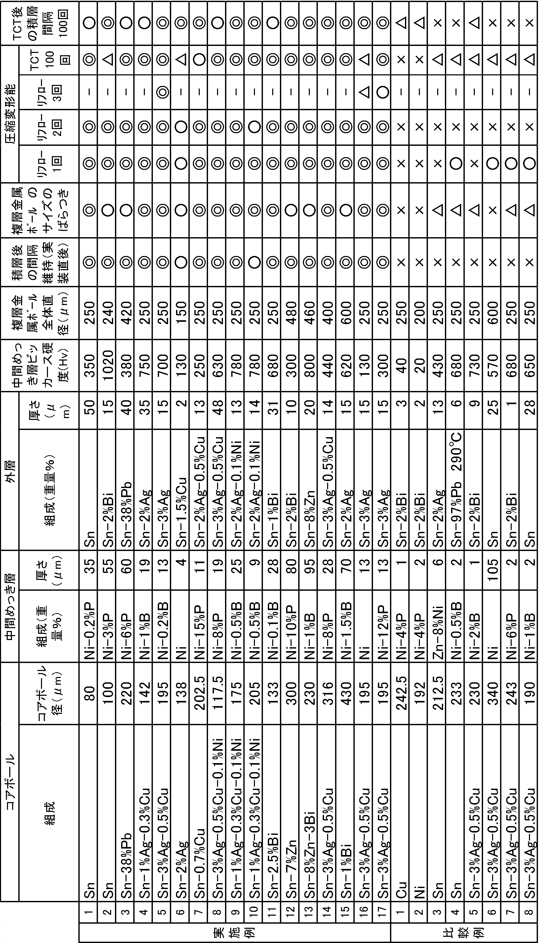
表1に示す「複層金属ボールのサイズのばらつき」に関しては、表1の実施例1~17、比較例1~8毎に、それぞれ試料数30個の複層金属ボールを用意し、各複層金属ボールをSEM観察により直径を測定してゆき、当該直径の標準偏差を求めた。表1の「複層金属ボールのサイズのばらつき」の欄では、標準偏差が3μm以下であればボール径が非常に安定しているため◎印、標準偏差が3μm超~6μm以下の範囲であればばらつきが少なく良好であるため○印、標準偏差が6μm超~10μm以下の範囲であれば実用上は問題ないが品質上は改善することが望ましいと判断して△印、標準偏差が10μm超であればサイズばらつきが大きく、実装時の高さのばらつき不良が問題となるため×印を、それぞれ表記した。
表1の「圧縮変形能」を調べるボール圧縮試験では、表1の実施例1~17、比較例1~8毎に2層構造のボールを作製し、この2層構造のボールを平面圧子により圧縮変形させながら、荷重と変形量の変化を測定して、ボールの変形抵抗を評価した。ここでは、中間めっき層の変形性を評価するため、上述したように、外層が形成されていない「中間めっき層とコアボールの2層構造のボール(中間製品)」を用いた。このボール圧縮試験において変形量が少ない場合には、中間めっき層が変形を抑制する機能が高いと判定できる。変形量はボールサイズに影響されるため、ボール圧縮試験を行う前の2層構造のボールのボール径に対する変形量の平均値を「圧縮変形能」として評価した。ここでは、実施例1~17、比較例1~8毎に、それぞれ10個の2層構造のボールを用意し、これら2層構造のボールに対してボール圧縮試験を行い200gfの荷重を負荷したときの変形量の平均値を測定した。
ボール圧縮試験では、中間めっき層とコアボールの2層構造のボール単体に対して、4種類の条件で「圧縮変形能」を調べた。具体的には、2層構造のボールに対してリフロー処理を1回施したとき、2層構造のボールに対してリフロー処理を2回施したとき、2層構造のボールに対してリフロー処理を3回施したとき、2層構造のボールに対してTCT処理を100サイクル施したとき、の4種類について「圧縮変形能」を調べた。ただし、リフロー処理を3回施す試験については、実施例5、16、17に対してだけ行った。リフロー処理は、上記の「リフロー工程」(N2フロー雰囲気下、130~200℃の範囲で1~3分、予備加熱を行った後に、最高温度230~300℃の温度範囲で0.5~1.5分ほど加熱)のときと同じ条件で行った。TCT処理は、上記の「TCT」(-40℃で30分間維持した後、125℃で30分間維持する一連の工程を1サイクル)のときと同じ条件で行った。
表1の「圧縮変形能」の欄では、変形量が15%以下であれば変形を抑える機能は良好であると判断して◎印、変形量が15%超~30%以下の範囲であれば硬さは良好であると判断して○印、変形量が30%超~50%以下の範囲であれば実用上は問題ないが品質上は改善することが望ましいと判断して△印、変形量が50%超であれば実装時の高さのばらつきが問題とるため×印を、それぞれ表記した。
表1における「積層後の間隔維持(実装直後)」と、「TCT後の積層間隔100回」とについては、下記のようにして評価を行った。複層金属ボールにより実装された試料(実装試料)の半導体素子と基板との間隔(積層間隔)の測定には、平坦な試料台の上に前記実装試料を設置して、半導体素子の高さと基板の高さとを測定して、その差分により積層間隔を求めた。測定位置は、4隅のコーナー近傍で測定した。1つの実装試料当たり4箇所の積層間隔の値を求め、その平均値を実装試料1個の積層間隔とした。こうした測定を、10個の実装試料で実施して、その平均値と標準偏差とを算出した。上記の高さ測定には光学顕微鏡などを用いた。
そして、TCTを行う前の実装直後の実装試料について積層間隔を調べた結果を、表1の「積層後の間隔維持(実装直後)」の欄に示し、TCTを100サイクル施した実装試料について積層間隔を調べた結果を、表1の「TCT後の積層間隔100回」の欄に示す。
表1の「TCT後の積層間隔100回」の欄には、積層間隔の標準偏差が0.5μm以下であれば、積層間隔を安定化させるスペーサ機能が優れていると判断して◎印、当該標準偏差が0.5μm超~1μm以下の範囲であれば良好であると判断して○印、当該標準偏差が1μm超~2μm以下の範囲であれば実用上は問題ないが品質上は改善することが望ましいと判断して△印、当該標準偏差が2μm超であれば実装時の高さのばらつが問題とるため×印を、それぞれ表記した。
また、表1の「積層後の間隔維持(実装直後)」の欄には、積層間隔の平均値がコアボールの直径(コアボール径)と等しく積層間隔を維持できているものをスペーサ機能が優れていると判断して◎印、コアボールの直径よりも0.5~2μm外れた範囲であれば良好であると判断して○印、コアボールの直径から2μm超外れた範囲であれば実装時の高さを維持できておらず問題があるため×印を、それぞれ表記した。
実施例1~17は、SnまたはSn合金からなるコアボールと、NiまたはNi合金からなる中間めっき層と、SnまたはSn合金からなる外層と、により構成され、中間めっき層の厚さが3~100μmである構成をすべて満足する複層金属ボールである。このような構成をすべて満足した実施例1~17の複層金属ボールでは、実装直後の積層間隔を維持しており、複層金属ボールのサイズのばらつきも小さいことなど、優れたスペーサ機能が確認された。それに対して、比較例1~8では、上述したいずれかの構成を満足していないため、実装直後の積層間隔、もしくは複層金属ボールのサイズのばらつきに問題が生じることが確認された。
上述したように、実施例1~17は、中間めっき層をNiまたはNi合金で形成し、かつ中間めっき層の厚さが3~100μmの範囲であるため、ボールサイズのばらつきが低く抑えられていたが、そのなかでも実施例1、4、5、7~11、14、16、17は、中間めっき層の厚さが5~50μmの範囲であるため、特にばらつきが良好に抑えられていた。
実施例1~17は、中間めっき層の厚さが3~100μmの範囲であるため、リフロー1回後の圧縮変形能が良好であるが、そのなかでも実施例1~5、7~17は、中間めっき層の厚さが5~100μmの範囲であるため、リフロー1回後の圧縮変形能が特に良好であった。また、実施例1~5、7~9、11~17では、中間めっき層の厚さが10~100μmの範囲であるため、リフロー2回後の圧縮変形能でも良好な結果が得られた。
実施例1、3~5、7~15、17は、中間めっき層のビッカース硬度が150~1000Hvの範囲であるため、TCTを100サイクル実施した後の圧縮変形能の評価が「○」以上となり良好であった。なかでも実施例1、3~5、8~15、17は硬さが300~1000Hvの範囲であるため、TCTを100サイクル実施した後の圧縮変形能の評価が「◎」となり、より良好であった。
実施例1~17は、さらに、外層の厚さが2~50μmの範囲であるため、TCT後の積層間隔が良好であり、実装後の熱サイクル評価で優れた接合信頼性を有することが確認できた。そのなかでも実施例2、5~7、9、10、12~17は、外層の厚さが2~30μmの範囲であるため、TCT後の積層間隔がより優れていた。
実施例5、16、17については、リフロー処理を3回施した「圧縮変形能」についても行っているが、中間めっき層の組成の違いによる圧縮変形能を評価したものであり、何れのボールも3回目のリフローにおいても実用上問題ないことを確認した。その中でも実施例5、17は中間めっき層の硬度が300Hv以上あるため変形が少なく、さらにその中でも実施例5において中間めっき層の硬度が500Hv以上あるため特に良好な結果であった。
Claims (5)
- SnまたはSn合金からなるコアボールと、
NiまたはNi合金からなり、前記コアボールを覆う中間めっき層と、
SnまたはSn合金からなり、前記中間めっき層を覆う外層と、により構成されており、
前記中間めっき層の厚さが3μm以上100μm以下である
ことを特徴とする複層金属ボール。 - 前記コアボールがAg、Cu、Ni、Zn、Bi、Inのいずれか1種以上を少なくとも0.02質量%以上含む
ことを特徴とする請求項1に記載の複層金属ボール。 - 前記中間めっき層のビッカース硬度が150Hv以上1000Hv以下である
ことを特徴とする請求項1または2に記載の複層金属ボール。 - 前記コアボールの直径が60μm以上500μm以下である
ことを特徴とする請求項1~3のいずれか1項に記載の複層金属ボール。 - 前記外層の厚さが2μm以上50μm以下である
ことを特徴とする請求項1~4のいずれか1項に記載の複層金属ボール。
Applications Claiming Priority (2)
| Application Number | Priority Date | Filing Date | Title |
|---|---|---|---|
| JP2016-184895 | 2016-09-21 | ||
| JP2016184895 | 2016-09-21 |
Publications (1)
| Publication Number | Publication Date |
|---|---|
| WO2018056313A1 true WO2018056313A1 (ja) | 2018-03-29 |
Family
ID=61691000
Family Applications (1)
| Application Number | Title | Priority Date | Filing Date |
|---|---|---|---|
| PCT/JP2017/033931 Ceased WO2018056313A1 (ja) | 2016-09-21 | 2017-09-20 | 複層金属ボール |
Country Status (1)
| Country | Link |
|---|---|
| WO (1) | WO2018056313A1 (ja) |
Cited By (3)
| Publication number | Priority date | Publication date | Assignee | Title |
|---|---|---|---|---|
| CN112362015A (zh) * | 2020-06-29 | 2021-02-12 | 泰安晶品新材料科技有限公司 | 一种集成电路封装用bga锡球的检测方法 |
| EP3950982A4 (en) * | 2019-10-25 | 2023-01-18 | Senju Metal Industry Co., Ltd. | NUCLEAR MATERIAL AND METHOD OF MAKING AN ELECTRONIC COMPONENT AND BUMP ELECTRODE |
| TWI877220B (zh) * | 2019-09-19 | 2025-03-21 | 日商積水化學工業股份有限公司 | 接著劑及天線裝置 |
Citations (4)
| Publication number | Priority date | Publication date | Assignee | Title |
|---|---|---|---|---|
| JP2003225790A (ja) * | 2002-02-05 | 2003-08-12 | Sharp Corp | 高純度Sn粒子を含有する接合材料、ならびに実装回路基板、実装パッケージおよびそれらの解体方法 |
| JP2009095865A (ja) * | 2007-10-17 | 2009-05-07 | Sekisui Chem Co Ltd | ニッケル担持ハンダボール |
| WO2013141166A1 (ja) * | 2012-03-23 | 2013-09-26 | 株式会社Neomaxマテリアル | はんだ被覆ボールおよびその製造方法 |
| JP2016155173A (ja) * | 2015-02-25 | 2016-09-01 | エムケイ電子株式会社 | 無フラックス接合用ソルダボール、その製造方法及びソルダバンプ形成方法 |
-
2017
- 2017-09-20 WO PCT/JP2017/033931 patent/WO2018056313A1/ja not_active Ceased
Patent Citations (4)
| Publication number | Priority date | Publication date | Assignee | Title |
|---|---|---|---|---|
| JP2003225790A (ja) * | 2002-02-05 | 2003-08-12 | Sharp Corp | 高純度Sn粒子を含有する接合材料、ならびに実装回路基板、実装パッケージおよびそれらの解体方法 |
| JP2009095865A (ja) * | 2007-10-17 | 2009-05-07 | Sekisui Chem Co Ltd | ニッケル担持ハンダボール |
| WO2013141166A1 (ja) * | 2012-03-23 | 2013-09-26 | 株式会社Neomaxマテリアル | はんだ被覆ボールおよびその製造方法 |
| JP2016155173A (ja) * | 2015-02-25 | 2016-09-01 | エムケイ電子株式会社 | 無フラックス接合用ソルダボール、その製造方法及びソルダバンプ形成方法 |
Cited By (4)
| Publication number | Priority date | Publication date | Assignee | Title |
|---|---|---|---|---|
| TWI877220B (zh) * | 2019-09-19 | 2025-03-21 | 日商積水化學工業股份有限公司 | 接著劑及天線裝置 |
| EP3950982A4 (en) * | 2019-10-25 | 2023-01-18 | Senju Metal Industry Co., Ltd. | NUCLEAR MATERIAL AND METHOD OF MAKING AN ELECTRONIC COMPONENT AND BUMP ELECTRODE |
| US11872656B2 (en) | 2019-10-25 | 2024-01-16 | Senju Metal Industry Co., Ltd. | Core material, electronic component and method for forming bump electrode |
| CN112362015A (zh) * | 2020-06-29 | 2021-02-12 | 泰安晶品新材料科技有限公司 | 一种集成电路封装用bga锡球的检测方法 |
Similar Documents
| Publication | Publication Date | Title |
|---|---|---|
| US9333593B2 (en) | Joining method, joint structure and method for producing the same | |
| Mei et al. | Kirkendall voids at Cu/solder interface and their effects on solder joint reliability | |
| US9475145B2 (en) | Solder bump joint in a device including lamellar structures | |
| KR20190040951A (ko) | 핵재료 및 반도체 패키지 및 범프 전극의 형성 방법 | |
| KR20050042060A (ko) | 땜납 피복 볼 및 그 제조방법과 반도체 접속구조의 형성방법 | |
| KR20140110926A (ko) | 접합 방법, 접합 구조체 및 그 제조 방법 | |
| JP2010245390A (ja) | ボンディングワイヤ | |
| TWI579992B (zh) | 半導體裝置及製造該半導體裝置之方法 | |
| KR20160003078A (ko) | 무연 솔더 접속을 위한 리드 프레임 구조체 | |
| US9079272B2 (en) | Solder joint with a multilayer intermetallic compound structure | |
| US20140291021A1 (en) | Junction structure for an electronic device and electronic device | |
| US9789569B2 (en) | Solder material and bonded structure | |
| JP5376356B2 (ja) | 電子素子の実装方法および該実装方法によって実装された電子部品 | |
| KR101983510B1 (ko) | 핵재료 및 납땜 이음 및 범프 전극의 형성 방법 | |
| JP2010103377A (ja) | はんだバンプを有する電子部材 | |
| US8822326B2 (en) | Method for manufacturing Sn alloy bump | |
| WO2018056314A1 (ja) | 複層金属ボール | |
| WO2018056315A1 (ja) | 複層金属ボール | |
| JP4175858B2 (ja) | はんだ被覆ボールの製造方法 | |
| KR20220091404A (ko) | 무연 솔더 합금, 그를 포함하는 솔더 페이스트, 및 그를 포함하는 반도체 부품 | |
| Kim et al. | Effects of PCB pad metal finishes on the Cu-pillar/Sn-Ag micro bump joint reliability of chip-on-board (COB) assembly | |
| JP5884513B2 (ja) | Pbフリーはんだ | |
| JP5552957B2 (ja) | 端子構造、プリント配線板、モジュール基板及び電子デバイス | |
| KR102579478B1 (ko) | 전기접속용 금속핀 | |
| KR102579479B1 (ko) | 접속핀 |
Legal Events
| Date | Code | Title | Description |
|---|---|---|---|
| 121 | Ep: the epo has been informed by wipo that ep was designated in this application |
Ref document number: 17853083 Country of ref document: EP Kind code of ref document: A1 |
|
| NENP | Non-entry into the national phase |
Ref country code: DE |
|
| 122 | Ep: pct application non-entry in european phase |
Ref document number: 17853083 Country of ref document: EP Kind code of ref document: A1 |
|
| NENP | Non-entry into the national phase |
Ref country code: JP |