WO2018043610A1 - 弾性波フィルタ装置、高周波フロントエンド回路及び通信装置 - Google Patents
弾性波フィルタ装置、高周波フロントエンド回路及び通信装置 Download PDFInfo
- Publication number
- WO2018043610A1 WO2018043610A1 PCT/JP2017/031271 JP2017031271W WO2018043610A1 WO 2018043610 A1 WO2018043610 A1 WO 2018043610A1 JP 2017031271 W JP2017031271 W JP 2017031271W WO 2018043610 A1 WO2018043610 A1 WO 2018043610A1
- Authority
- WO
- WIPO (PCT)
- Prior art keywords
- parallel arm
- arm resonator
- circuit
- parallel
- filter
- Prior art date
- Legal status (The legal status is an assumption and is not a legal conclusion. Google has not performed a legal analysis and makes no representation as to the accuracy of the status listed.)
- Ceased
Links
Images









Classifications
-
- H—ELECTRICITY
- H03—ELECTRONIC CIRCUITRY
- H03H—IMPEDANCE NETWORKS, e.g. RESONANT CIRCUITS; RESONATORS
- H03H9/00—Networks comprising electromechanical or electro-acoustic elements; Electromechanical resonators
- H03H9/46—Filters
- H03H9/64—Filters using surface acoustic waves
- H03H9/6489—Compensation of undesirable effects
- H03H9/6496—Reducing ripple in transfer characteristic
-
- H—ELECTRICITY
- H03—ELECTRONIC CIRCUITRY
- H03H—IMPEDANCE NETWORKS, e.g. RESONANT CIRCUITS; RESONATORS
- H03H9/00—Networks comprising electromechanical or electro-acoustic elements; Electromechanical resonators
- H03H9/46—Filters
- H03H9/64—Filters using surface acoustic waves
- H03H9/6489—Compensation of undesirable effects
-
- H—ELECTRICITY
- H01—ELECTRIC ELEMENTS
- H01Q—ANTENNAS, i.e. RADIO AERIALS
- H01Q1/00—Details of, or arrangements associated with, antennas
- H01Q1/50—Structural association of antennas with earthing switches, lead-in devices or lightning protectors
-
- H—ELECTRICITY
- H03—ELECTRONIC CIRCUITRY
- H03H—IMPEDANCE NETWORKS, e.g. RESONANT CIRCUITS; RESONATORS
- H03H9/00—Networks comprising electromechanical or electro-acoustic elements; Electromechanical resonators
- H03H9/02—Details
- H03H9/02535—Details of surface acoustic wave devices
- H03H9/02637—Details concerning reflective or coupling arrays
-
- H—ELECTRICITY
- H03—ELECTRONIC CIRCUITRY
- H03H—IMPEDANCE NETWORKS, e.g. RESONANT CIRCUITS; RESONATORS
- H03H9/00—Networks comprising electromechanical or electro-acoustic elements; Electromechanical resonators
- H03H9/02—Details
- H03H9/125—Driving means, e.g. electrodes, coils
- H03H9/145—Driving means, e.g. electrodes, coils for networks using surface acoustic waves
- H03H9/14538—Formation
-
- H—ELECTRICITY
- H03—ELECTRONIC CIRCUITRY
- H03H—IMPEDANCE NETWORKS, e.g. RESONANT CIRCUITS; RESONATORS
- H03H9/00—Networks comprising electromechanical or electro-acoustic elements; Electromechanical resonators
- H03H9/02—Details
- H03H9/125—Driving means, e.g. electrodes, coils
- H03H9/145—Driving means, e.g. electrodes, coils for networks using surface acoustic waves
- H03H9/14538—Formation
- H03H9/14541—Multilayer finger or busbar electrode
-
- H—ELECTRICITY
- H03—ELECTRONIC CIRCUITRY
- H03H—IMPEDANCE NETWORKS, e.g. RESONANT CIRCUITS; RESONATORS
- H03H9/00—Networks comprising electromechanical or electro-acoustic elements; Electromechanical resonators
- H03H9/02—Details
- H03H9/125—Driving means, e.g. electrodes, coils
- H03H9/145—Driving means, e.g. electrodes, coils for networks using surface acoustic waves
- H03H9/14544—Transducers of particular shape or position
-
- H—ELECTRICITY
- H03—ELECTRONIC CIRCUITRY
- H03H—IMPEDANCE NETWORKS, e.g. RESONANT CIRCUITS; RESONATORS
- H03H9/00—Networks comprising electromechanical or electro-acoustic elements; Electromechanical resonators
- H03H9/46—Filters
- H03H9/54—Filters comprising resonators of piezoelectric or electrostrictive material
- H03H9/542—Filters comprising resonators of piezoelectric or electrostrictive material including passive elements
-
- H—ELECTRICITY
- H03—ELECTRONIC CIRCUITRY
- H03H—IMPEDANCE NETWORKS, e.g. RESONANT CIRCUITS; RESONATORS
- H03H9/00—Networks comprising electromechanical or electro-acoustic elements; Electromechanical resonators
- H03H9/46—Filters
- H03H9/54—Filters comprising resonators of piezoelectric or electrostrictive material
- H03H9/58—Multiple crystal filters
- H03H9/60—Electric coupling means therefor
- H03H9/605—Electric coupling means therefor consisting of a ladder configuration
-
- H—ELECTRICITY
- H03—ELECTRONIC CIRCUITRY
- H03H—IMPEDANCE NETWORKS, e.g. RESONANT CIRCUITS; RESONATORS
- H03H9/00—Networks comprising electromechanical or electro-acoustic elements; Electromechanical resonators
- H03H9/46—Filters
- H03H9/64—Filters using surface acoustic waves
- H03H9/6403—Programmable filters
-
- H—ELECTRICITY
- H03—ELECTRONIC CIRCUITRY
- H03H—IMPEDANCE NETWORKS, e.g. RESONANT CIRCUITS; RESONATORS
- H03H9/00—Networks comprising electromechanical or electro-acoustic elements; Electromechanical resonators
- H03H9/46—Filters
- H03H9/64—Filters using surface acoustic waves
- H03H9/6423—Means for obtaining a particular transfer characteristic
- H03H9/6433—Coupled resonator filters
-
- H—ELECTRICITY
- H03—ELECTRONIC CIRCUITRY
- H03H—IMPEDANCE NETWORKS, e.g. RESONANT CIRCUITS; RESONATORS
- H03H9/00—Networks comprising electromechanical or electro-acoustic elements; Electromechanical resonators
- H03H9/46—Filters
- H03H9/64—Filters using surface acoustic waves
- H03H9/6423—Means for obtaining a particular transfer characteristic
- H03H9/6433—Coupled resonator filters
- H03H9/6483—Ladder SAW filters
-
- H—ELECTRICITY
- H04—ELECTRIC COMMUNICATION TECHNIQUE
- H04B—TRANSMISSION
- H04B1/00—Details of transmission systems, not covered by a single one of groups H04B3/00 - H04B13/00; Details of transmission systems not characterised by the medium used for transmission
- H04B1/005—Details of transmission systems, not covered by a single one of groups H04B3/00 - H04B13/00; Details of transmission systems not characterised by the medium used for transmission adapting radio receivers, transmitters andtransceivers for operation on two or more bands, i.e. frequency ranges
- H04B1/0053—Details of transmission systems, not covered by a single one of groups H04B3/00 - H04B13/00; Details of transmission systems not characterised by the medium used for transmission adapting radio receivers, transmitters andtransceivers for operation on two or more bands, i.e. frequency ranges with common antenna for more than one band
- H04B1/0057—Details of transmission systems, not covered by a single one of groups H04B3/00 - H04B13/00; Details of transmission systems not characterised by the medium used for transmission adapting radio receivers, transmitters andtransceivers for operation on two or more bands, i.e. frequency ranges with common antenna for more than one band using diplexing or multiplexing filters for selecting the desired band
-
- H—ELECTRICITY
- H04—ELECTRIC COMMUNICATION TECHNIQUE
- H04B—TRANSMISSION
- H04B1/00—Details of transmission systems, not covered by a single one of groups H04B3/00 - H04B13/00; Details of transmission systems not characterised by the medium used for transmission
- H04B1/005—Details of transmission systems, not covered by a single one of groups H04B3/00 - H04B13/00; Details of transmission systems not characterised by the medium used for transmission adapting radio receivers, transmitters andtransceivers for operation on two or more bands, i.e. frequency ranges
- H04B1/0053—Details of transmission systems, not covered by a single one of groups H04B3/00 - H04B13/00; Details of transmission systems not characterised by the medium used for transmission adapting radio receivers, transmitters andtransceivers for operation on two or more bands, i.e. frequency ranges with common antenna for more than one band
- H04B1/006—Details of transmission systems, not covered by a single one of groups H04B3/00 - H04B13/00; Details of transmission systems not characterised by the medium used for transmission adapting radio receivers, transmitters andtransceivers for operation on two or more bands, i.e. frequency ranges with common antenna for more than one band using switches for selecting the desired band
-
- H—ELECTRICITY
- H04—ELECTRIC COMMUNICATION TECHNIQUE
- H04B—TRANSMISSION
- H04B1/00—Details of transmission systems, not covered by a single one of groups H04B3/00 - H04B13/00; Details of transmission systems not characterised by the medium used for transmission
- H04B1/38—Transceivers, i.e. devices in which transmitter and receiver form a structural unit and in which at least one part is used for functions of transmitting and receiving
- H04B1/40—Circuits
Definitions
- the present invention relates to an elastic wave filter device having a resonator, a high-frequency front-end circuit, and a communication device.
- an elastic wave filter device such as a ladder filter
- a configuration in which a plurality of parallel arm resonators are provided for one parallel arm (parallel arm resonance circuit) connecting a series arm (series arm resonance circuit) and the ground is known.
- a plurality of parallel arm resonators having different resonance frequencies are provided in one parallel arm in a state of being connected in series, thereby improving the skirt characteristic (damping slope) of the filter.
- a resonator using an elastic wave includes an IDT (InterDigital Transducer) electrode having a periodic structure composed of a plurality of conductor strips (electrode fingers) arranged periodically and a reflector (reflector). For this reason, such a resonator has a frequency band which reflects an elastic wave in a specific frequency region with a high reflection coefficient.
- This frequency band is generally called a stop band and is defined by the repetition period of the periodic structure. At this time, a ripple in which the reflection coefficient locally fluctuates easily at the high band end of the stop band.
- the stop band high band end of the parallel arm resonator having a low frequency may be located in the pass band or in the vicinity of the high band end of the pass band. Therefore, in this case, if a ripple is generated at the high end of the stop band of the parallel arm resonator, the loss in the pass band increases.
- an object of the present invention is to provide an elastic wave filter device, a high-frequency front-end circuit, and a communication device that can suppress loss in the passband.
- an elastic wave filter device includes a series arm including one or more elastic wave resonators connected between a first input / output terminal and a second input / output terminal.
- a first parallel arm resonator and a second parallel arm resonator connected between a resonance circuit and the same node of the path connecting the first input / output terminal and the second input / output terminal and the ground;
- a resonance frequency in the first parallel arm resonator is lower than a resonance frequency in the second parallel arm resonator, and an anti-resonance frequency in the first parallel arm resonator is in the second parallel arm resonator.
- the first parallel arm resonator has an IDT electrode that excites an elastic wave and a reflector that reflects the elastic wave excited by the IDT electrode, and has an IDT electrode lower than the antiresonance frequency.
- Serial pitch of the IDT electrode and the reflector is less than or more and 0.50 ⁇ 0.42 ⁇ .
- the inventors of the present application have found that the loss in the passband can be suppressed by setting the IR pitch of the first parallel arm resonator to 0.42 ⁇ or more and less than 0.50 ⁇ . Specifically, if the IR pitch is increased too much, the ripple in the high band end of the stop band of the first parallel arm resonator increases, thereby increasing the loss in the passband. On the other hand, if the IR pitch is made too small, the ripple on the high frequency side of the first parallel arm resonator (specifically, between the resonance frequency and the anti-resonance frequency) becomes large, so Loss increases or the attenuation characteristics on the low pass band side deteriorate. Therefore, the loss in the pass band can be suppressed by keeping the IR pitch of the first parallel arm resonator within an appropriate range.
- the pitch between the IDT electrode and the reflector may be 0.44 ⁇ or more and 0.46 ⁇ or less.
- the present inventor has made the IR pitch of the first parallel arm resonator 0.44 ⁇ or more and 0.46 ⁇ or less, thereby increasing the loss in the passband and lowering the passband. It was found that the deterioration of the attenuation characteristics on the side can be more reliably suppressed. Specifically, when the IR pitch is increased to approach 0.50 ⁇ , the ripple on the high resonance frequency side of the first parallel arm resonator can be suppressed, but the stop band high region of the first parallel arm resonator can be suppressed. It becomes difficult to suppress the ripple at the end.
- the ripple at the high end of the stop band of the first parallel arm resonator can be suppressed, but the ripple on the high frequency side of the resonance frequency of the first parallel arm resonator is reduced. Deterrence becomes difficult. Therefore, by setting the IR pitch of the first parallel arm resonator to be 0.44 ⁇ or more and 0.46 ⁇ or less, the ripple at the high band end of the stop band and the ripple at the resonance frequency high band side of the first parallel arm resonator. Since both of these can be suppressed, the loss in a passband can be suppressed more reliably.
- the impedance circuit in which a pair of impedance elements and a switch element are connected in parallel, and at least one of the first parallel arm resonator and the second parallel arm resonator is connected in series with the impedance circuit. You may decide.
- the second parallel arm resonator is connected in series with the impedance circuit, and the first parallel arm resonator is connected in parallel to a circuit in which the second parallel arm resonator and the impedance circuit are connected in series. It may be connected.
- the first characteristic and the second characteristic are suppressed while suppressing the increase of the insertion loss at the high end of the pass band while switching the frequency of the attenuation pole on the high side of the pass band in accordance with switching between the conduction and the non-conduction of the switch element.
- a tunable filter for switching characteristics can be provided.
- the first parallel arm resonator is connected in series with the impedance circuit, and the second parallel arm resonator is connected in parallel to a circuit in which the first parallel arm resonator and the impedance circuit are connected in series. It may be connected.
- the first characteristic and the second characteristic are suppressed while suppressing the increase of the insertion loss at the low end of the passband while switching the frequency of the attenuation pole on the low passband side according to the switching of the switch element.
- a tunable filter for switching characteristics can be provided.
- first parallel arm resonator and the second parallel arm resonator are connected in parallel
- the impedance circuit includes the first parallel arm resonator and the second parallel arm resonator connected in parallel. You may decide to be connected in series with respect to the circuit.
- two impedance circuits in which a pair of impedance elements and a switch element are arranged in parallel are provided, and the first parallel arm resonator is connected in series with one impedance circuit of the two impedance circuits, and the first The two parallel arm resonators are connected in series with the other impedance circuit of the two impedance circuits, the circuit in which the first parallel arm resonator and the one impedance circuit are connected in series, and the second parallel arm The circuit in which the resonator and the other impedance circuit are connected in series may be connected in parallel.
- the frequency of the attenuation pole on the high side of the passband and the low side of the passband can be switched according to the switching of the conduction and non-conduction of the switch element, and the high end of the passband and the low end of the passband It is possible to provide a tunable filter that can suppress an increase in insertion loss. Therefore, such a tunable filter can switch the center frequency while maintaining the bandwidth, for example.
- the first parallel arm resonator and the second parallel arm further include a switch element connected in parallel to one parallel arm resonator of the first parallel arm resonator and the second parallel arm resonator.
- the other parallel arm resonator of the resonator may be connected in series to a circuit in which the one parallel arm resonator and the switch element are connected in parallel.
- the frequency of the attenuation pole on the low passband side can be switched and the number of attenuation poles on the high passband side can be switched according to switching between conduction and non-conduction of the switch element.
- a high-frequency front-end circuit includes any one of the elastic wave filter devices described above and an amplifier circuit connected to the elastic wave filter device.
- a communication device includes an RF signal processing circuit that processes a high-frequency signal transmitted and received by an antenna element, and the high-frequency signal that is transmitted between the antenna element and the RF signal processing circuit. And a high-frequency front-end circuit.
- the elastic wave filter device According to the elastic wave filter device, the high-frequency front end circuit, and the communication device according to the present invention, it is possible to suppress loss in the passband.
- FIG. 1A is a circuit configuration diagram of a filter according to Embodiment 1.
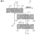
- FIG. 1B is a plan view schematically showing the electrode structure of the filter according to Embodiment 1.
- FIG. 2 is an example of a diagram schematically illustrating the structure of the parallel arm resonator according to the first embodiment.
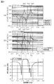
- FIG. 3 is a graph showing the characteristics of the filter according to the first embodiment.
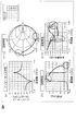
- FIG. 4 is a graph showing a change in characteristics when the IR pitch is changed in a typical resonator.
- FIG. 5A is a graph showing the absolute value of the impedance of the parallel arm resonator.
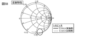
- FIG. 5B is a graph representing the impedance of the parallel arm resonator in a Smith chart.
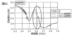
- FIG. 5C is a graph showing the reflection loss of the parallel arm resonator.
- FIG. 6 is a graph showing filter characteristics for Examples and Comparative Examples.
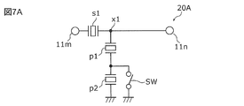
- FIG. 7A is a circuit configuration diagram of a filter in application example 1 of the second embodiment.
- FIG. 7B is a graph showing the filter characteristics of the filter in application example 1 of the second embodiment.
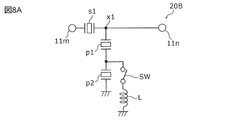
- FIG. 8A is a circuit configuration diagram of a filter in application example 2 of the second embodiment.
- FIG. 8B is a graph showing the filter characteristics of the filter in application example 2 of the second embodiment.
- FIG. 9A is a circuit configuration diagram of a filter in application example 3 of the second embodiment.
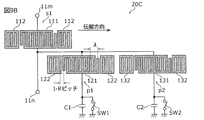
- FIG. 9B is a plan view schematically illustrating the electrode structure of the filter in application example 3 of the second embodiment.
- FIG. 9C is a graph illustrating filter characteristics in application example 3 of the second exemplary embodiment.
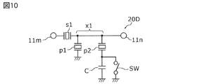
- FIG. 10 is a circuit configuration diagram of a filter in application example 4 of the second embodiment.
- FIG. 11 is a circuit configuration diagram of a filter in application example 5 of the second embodiment.
- FIG. 12 is a circuit configuration diagram of a filter in application example 6 of the second embodiment.
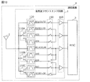
- FIG. 13 is a configuration diagram of a high-frequency front-end circuit and its peripheral circuits according to the third embodiment.
- pass band low band end means “the lowest frequency in the pass band”.
- Passband high band end means “the highest frequency in the passband”.
- pass band lower band side means “outside the pass band and lower frequency side than the pass band”.
- passband high band side means “outside of the pass band and higher in frequency than the pass band”.
- FIG. 1A is a circuit configuration diagram of a filter 10 according to the first embodiment.
- the filter 10 is a high-frequency filter circuit that is disposed, for example, in the front-end portion of a multimode / multiband mobile phone.
- the filter 10 is a band-pass filter that is built in a multi-band compatible mobile phone that complies with a communication standard such as LTE (Long Term Evolution) and filters high-frequency signals in a predetermined band.
- the filter 10 is an elastic wave filter device that filters high-frequency signals using an elastic wave resonator.
- the filter 10 includes a series arm resonator s1 and parallel arm resonators p1 and p2.
- the series arm resonator s1 is connected between the input / output terminal 11m (first input / output terminal) and the input / output terminal 11n (second input / output terminal). That is, the series arm resonator s1 is a series arm resonance circuit provided on a path connecting the input / output terminal 11m and the input / output terminal 11n. Note that the path is not limited to the series arm resonator s1, but may be provided with a series arm resonance circuit including one or more elastic wave resonators. In the present embodiment, the series arm resonance circuit is configured by one elastic wave resonator, but may be configured by a plurality of elastic wave resonators.
- the series arm resonance circuit including a plurality of elastic wave resonators includes, for example, a longitudinally coupled resonator including a plurality of elastic wave resonators, or a plurality of divided resonances in which one elastic wave resonator is divided in series. Includes children. For example, by using a longitudinally coupled resonator as the series arm resonance circuit, it becomes possible to adapt to required filter characteristics such as enhancement of attenuation.
- the parallel arm resonator p1 is a first parallel arm resonator connected to a node (node x1 in FIG. 1A) and a ground (reference terminal) on a path connecting the input / output terminal 11m and the input / output terminal 11n. . That is, the parallel arm resonator p1 is a resonator provided in a parallel arm resonance circuit that connects the node x1 on the path and the ground.
- the parallel arm resonator p2 is a second parallel arm resonator connected to a node (node x1 in FIG. 1A) and a ground (reference terminal) on the path connecting the input / output terminal 11m and the input / output terminal 11n. . That is, the parallel arm resonator p2 is a resonator provided in a parallel arm resonance circuit that connects the node x1 on the path and the ground.
- the resonance frequency in the parallel arm resonator p1 is lower than the resonance frequency in the parallel arm resonator p2, and the antiresonance frequency in the parallel arm resonator p1 is lower than the antiresonance frequency in the parallel arm resonator p2.
- the resonance frequency in the resonator is a frequency of a “resonance point” that is a singular point (ideally a point where the impedance is 0) at which the impedance of the resonator is minimized.
- the antiresonance frequency in the resonator is a frequency of an “antiresonance point” that is a singular point (ideally an infinite point) where the impedance of the resonator becomes a maximum.
- the parallel arm resonators p1 and p2 are connected in series, and are connected between the node x1 and the ground.
- the parallel arm resonator p1 has one terminal connected to the node x1 and the other terminal connected to one terminal of the parallel arm resonator p2.
- the parallel arm resonator p2 has one terminal connected to the other terminal of the parallel arm resonator p1, and the other terminal connected to the ground.
- the connection order of the parallel arm resonators p1 and p2 is not limited to this, and the connection order may be reversed.
- the parallel arm resonators p1 and p2 are configured by one elastic wave resonator. However, at least one of the parallel arm resonators p1 and p2 may be configured by a plurality of split resonators in which one elastic wave resonator is split in series or in parallel.
- the parallel arm resonators p1 and p2 constitute a parallel arm resonance circuit connected between the node x1 on the path connecting the input / output terminal 11m and the input / output terminal 11n and the ground. That is, the parallel arm resonance circuit is provided in one path connecting the path and the ground. Therefore, the filter 10 has a one-stage ladder-type filter structure including a series arm resonator s1 and a parallel arm resonance circuit (parallel arm resonators p1 and p2 in the present embodiment).
- the parallel arm resonance circuit constituted by the parallel arm resonators p1 and p2 forms the passband of the filter 10 together with the series arm resonator s1.
- FIG. 1B is a plan view schematically showing the electrode structure of the filter 10 according to the first embodiment.
- each resonator (series arm resonator s1, parallel arm resonator p1 and p2) constituting the filter 10 is an elastic wave resonator using an elastic wave.
- the filter 10 can be constituted by an IDT electrode formed on a piezoelectric substrate, so that a small and low-profile filter circuit having a pass characteristic with improved steepness can be realized.
- the substrate having piezoelectricity is a substrate having piezoelectricity at least on the surface.
- the substrate may include a piezoelectric thin film on the surface, a film having a different sound velocity from the piezoelectric thin film, and a laminated body such as a support substrate.
- the substrate includes, for example, a laminate including a high sound speed support substrate and a piezoelectric thin film formed on the high sound speed support substrate, a high sound speed support substrate, and a low sound speed film formed on the high sound speed support substrate.
- a laminate including a piezoelectric thin film formed on the film may be used. Note that the substrate may have piezoelectricity throughout the substrate.
- the series arm resonator s1 and the parallel arm resonator p1 include an IDT electrode that excites an elastic wave, and a pair of reflectors that are arranged so as to sandwich the IDT electrode from both sides in the propagation direction of the elastic wave.
- the series arm resonator s1 includes an IDT electrode 111 and a pair of reflectors 112.
- the parallel arm resonator p ⁇ b> 1 includes an IDT electrode 121 and a set of reflectors 122.
- the parallel arm resonator p ⁇ b> 2 includes an IDT electrode 131 and a set of reflectors 132.
- the parallel arm resonator p1 (first parallel arm resonator) includes an IDT electrode 121 that excites an elastic wave having a longer wavelength than the IDT electrode 131 of the parallel arm resonator p2 (second parallel arm resonator), and the IDT electrode 121. And a reflector 122 that reflects the elastic wave excited in step (b).
- the pitch between the IDT electrode 121 and the reflector 122 is 0.42 ⁇ or more and less than 0.50 ⁇ , preferably 0.44 ⁇ or more and 0.46 ⁇ or less. This will be described later.
- each resonator constituting the filter 10 will be described in more detail by focusing on the parallel arm resonator p1.
- the other resonators have substantially the same structure as the parallel arm resonator p1 except that the IR pitch is configured to be about 0.5 times the wavelength ⁇ of the elastic wave. Description is omitted.
- FIG. 2 is an example of a diagram schematically showing the structure of the parallel arm resonator p1 in the present embodiment, where (a) is a plan view and (b) is a cross-sectional view of (a).
- the parallel arm resonator p ⁇ b> 1 shown in FIG. 2 is for explaining a typical structure of each resonator constituting the filter 10.
- the number and length of electrode fingers constituting the IDT electrode of each resonator of the filter 10 are not limited to the number and length of electrode fingers of the IDT electrode shown in FIG.
- the parallel arm resonator p1 includes an electrode film 101 constituting the IDT electrode 121 and the reflector 122, a piezoelectric substrate 102 on which the electrode film 101 is formed, A protective layer 103 covering the electrode film 101.
- an electrode film 101 constituting the IDT electrode 121 and the reflector 122
- a piezoelectric substrate 102 on which the electrode film 101 is formed
- a protective layer 103 covering the electrode film 101.
- the comb-tooth electrode 101a includes a plurality of electrode fingers 110a that are parallel to each other and a bus bar electrode 111a that connects the plurality of electrode fingers 110a.
- the comb-tooth electrode 101b includes a plurality of electrode fingers 110b that are parallel to each other and a bus bar electrode 111b that connects the plurality of electrode fingers 110b.
- the plurality of electrode fingers 110a and 110b are formed along a direction orthogonal to the propagation direction of the elastic wave, and are periodically formed along the propagation direction.
- the IDT electrode 121 configured as described above excites a surface acoustic wave in a specific frequency region defined by the electrode pitches of the plurality of electrode fingers 110a and 110b constituting the IDT electrode 121.
- each of the comb electrodes 101a and 101b may be referred to as an IDT electrode alone. However, in the following, for the sake of convenience, it is assumed that one IDT electrode 121 is constituted by a pair of comb-tooth electrodes 101a and 101b.
- the reflector 122 is disposed in the propagation direction of the elastic wave with respect to the IDT electrode 121. Specifically, the pair of reflectors 122 are arranged so as to sandwich the IDT electrode 121 from both sides in the elastic wave propagation direction.
- the reflector 122 includes a plurality of electrode fingers 210 that are parallel to each other, a bus bar electrode 211 that connects one end of the plurality of electrode fingers 210, and a bus bar electrode 211 that connects the other end of the plurality of electrode fingers 210.
- a pair of bus bar electrodes 211 is included.
- the plurality of electrode fingers 210 are formed along a direction orthogonal to the propagation direction of the elastic wave, and are periodically formed along the propagation direction, like the plurality of electrode fingers 110a and 110b constituting the IDT electrode 121. ing.
- the reflector 122 configured in this manner reflects a surface acoustic wave with a high reflection coefficient in a frequency band (stop band) defined by the electrode pitch of the plurality of electrode fingers 210 constituting the reflector 122. That is, when the electrode pitch of the IDT electrode 121 and the electrode pitch of the reflector 122 are equal, the reflector 122 reflects the surface acoustic wave excited by the IDT electrode 121 with a high reflection coefficient.
- the parallel arm resonator p1 can confine the excited surface acoustic wave and prevent it from leaking outside. Therefore, the parallel arm resonator p1 can improve the Q of the resonance frequency and the anti-resonance frequency defined by the electrode pitch, logarithm, crossover width, and the like of the IDT electrode 121.
- the reflector 122 should just have the electrode finger 210, and does not need to have the bus-bar electrode 211.
- the number of the electrode fingers 210 should just be one or more, and is not specifically limited. However, if the number of electrode fingers 210 is too small, the leakage of elastic waves increases, so that the filter characteristics can be deteriorated. On the other hand, when the number of the electrode fingers 210 is too large, the reflector 122 becomes large, so that the entire filter 10 can be enlarged. For this reason, the number of electrode fingers 210 can be appropriately determined in consideration of the filter characteristics and size required for the filter 10.
- the IDT electrode 121 and the reflector 122 are constituted by the electrode film 101 shown in FIG.
- the electrode film 101 has a stacked structure of an adhesion layer 101g and a main electrode layer 101h as shown in FIG.
- the IDT electrode 121 and the reflector 122 are composed of the same electrode film 101. However, they may be composed of electrode films having different structures or compositions.
- the adhesion layer 101g is a layer for improving adhesion between the piezoelectric substrate 102 and the main electrode layer 101h, and Ti is used as a material, for example.
- the film thickness of the adhesion layer 101g is, for example, 12 nm.
- the main electrode layer 101h is made of, for example, Al containing 1% Cu.
- the film thickness of the main electrode layer 101h is, for example, 162 nm.
- the piezoelectric substrate 102 is a substrate on which the electrode film 101 (that is, the IDT electrode 121 and the reflector 122) is formed, for example, LiTaO 3 piezoelectric single crystal, LiNbO 3 piezoelectric single crystal, KNbO 3 piezoelectric single crystal, crystal, or Made of piezoelectric ceramics.
- the protective layer 103 is formed to cover the comb electrodes 101a and 101b.
- the protective layer 103 is a layer for the purpose of protecting the main electrode layer 101h from the external environment, adjusting frequency temperature characteristics, and improving moisture resistance, for example, a film mainly composed of silicon dioxide. .
- each resonator which the filter 10 has is not limited to the structure described in FIG.
- the electrode film 101 may not be a stacked structure of metal films but may be a single layer of metal films.
- the materials constituting the adhesion layer 101g, the main electrode layer 101h, and the protective layer 103 are not limited to the materials described above.
- the electrode film 101 may be made of, for example, a metal or alloy such as Ti, Al, Cu, Pt, Au, Ag, or Pd, and is made of a plurality of laminated bodies made of the above metals or alloys. May be.
- the protective layer 103 may not be formed.
- the wavelength of the excited elastic wave is defined by the design parameters of the IDT electrode 121 and the like.
- the design parameters of the IDT electrode 121 that is, the design parameters of the comb electrode 101a and the comb electrode 101b will be described.
- the wavelength of the elastic wave is defined by the repetition period ⁇ of the plurality of electrode fingers 110a or 110b constituting the comb electrodes 101a and 101b shown in FIG.
- the electrode pitch (electrode period) is 1 ⁇ 2 of the repetition period ⁇
- the line width of the electrode fingers 110a and 110b constituting the comb electrodes 101a and 101b is W
- the adjacent electrode fingers 110a and electrodes When the space width between the finger 110b is S, it is defined by (W + S).
- the crossing width L of the IDT electrode 121 is obtained by viewing the electrode finger 110a of the comb electrode 101a and the electrode finger 110b of the comb electrode 101b from the propagation direction of the elastic wave.
- the electrode duty is the line width occupation ratio of the plurality of electrode fingers 110a and 110b, and is the ratio of the line width to the sum of the line width and the space width of the plurality of electrode fingers 110a and 110b. , W / (W + S).
- the film thickness of the IDT electrode 121 is the thickness h of the plurality of electrode fingers 110a and 110b.
- the electrode pitch (electrode period) of the reflector 122 is defined by (W REF + S REF ) when the line width of the electrode finger 210 is W REF and the space width between the adjacent electrode fingers 210 is S REF. .
- the electrode duty (duty ratio) of the reflector 122 is the line width occupation ratio of the plurality of electrode fingers 210, and is the ratio of the line width to the sum of the line width and the space width of the electrode fingers 210; It is defined by REF / (W REF + S REF ).
- the film thickness of the reflector 122 is the thickness of the plurality of electrode fingers 210.
- the electrode pitch and electrode duty of the reflector 122 are equivalent to the electrode pitch and electrode duty of the IDT electrode 121.
- the reflector 122 is disposed so that the pair of bus bar electrodes 211 overlap the bus bar electrodes 111 a and 111 b of the IDT electrode 121 when viewed from the propagation direction of the elastic wave.
- the reflector 122 preferably has the above configuration from the viewpoint of suppressing leakage of elastic waves, but may have a configuration different from the above configuration.
- the pitch (IR pitch) between the IDT electrode 121 and the reflector 122 is (i) the electrode finger closest to the reflector 122 among the plurality of electrode fingers 110a or 110b constituting the IDT electrode 121, and (ii) It is defined by the center-to-center distance with the electrode finger 210 closest to the IDT electrode 121 among the plurality of electrode fingers 210 constituting the reflector 122.
- This IR pitch can be expressed by using the repetition period ⁇ of the plurality of electrode fingers 110a or 110b constituting the comb electrodes 101a and 101b (that is, the wavelength ⁇ of the elastic wave determined by the electrode pitch of the IDT electrode 121). For example, in the case of 0.50 times the repetition period ⁇ , it is expressed as 0.50 ⁇ .
- a singular point where the impedance is minimized (ideally a point where the impedance is 0) is also referred to as a “resonance point” for convenience, not only for a single resonator but also for a circuit including a plurality of resonators.
- the frequency is called “resonance frequency”.
- a singular point where the impedance is maximum (ideally a point where the impedance is infinite) is called an “anti-resonance point”, and its frequency is called an “anti-resonance frequency”.
- FIG. 3 is a graph showing the characteristics of the filter 10 according to the first embodiment. Specifically, (a) of the figure is a graph showing impedance characteristics of the parallel arm resonators p1 and p2 and the series arm resonator s1.
- FIG. 4B is a graph showing the combined impedance characteristics (synthetic characteristics) of the parallel arm resonators p1 and p2 and the impedance characteristics of the series arm resonator s1.
- FIG. 4C is a graph showing the filter characteristics of the filter 10.
- the parallel arm resonator p1, the parallel arm resonator p2, and the series arm resonator s1 have the following impedance characteristics. Specifically, for the parallel arm resonator p1, the parallel arm resonator p2, and the series arm resonator s1, in this order, assuming that the resonance frequencies are frp1, frp2, frs1, and the antiresonance frequencies are fap1, fap2, and fas1, In this form, frp1 ⁇ frs1 ⁇ frp2 and fap1 ⁇ fas1 ⁇ fap2 are satisfied.
- the combined characteristic of the two parallel arm resonators (“parallel arm resonators p1 and p2) (“p1 + p2 combined characteristic” in the figure) is the resonance frequency frp1 of the parallel arm resonator p1.
- the combined characteristic becomes maximum at the antiresonance frequency fap1 of the parallel arm resonator p1 and the antiresonance frequency fap2 of the parallel arm resonator p2.
- a pass band is formed by the anti-resonance frequency (that is, fap1) on the lower side of the two anti-resonance frequencies of the parallel arm resonance circuit and the resonance frequency frs1 of the series arm resonator s1.
- an attenuation band having the frequency fr1 as an attenuation pole is formed on the low passband side, and the frequency fr2 and the above frequency fr2 are formed on the high passband side.
- An attenuation band having an anti-resonance frequency fas1 of the series arm resonator s1 as an attenuation pole is formed.
- the IR pitch is designed to be equal to the electrode pitch of the IDT electrode 121 (that is, 0.50 ⁇ ) in order to provide regularity in the propagation of elastic waves.
- the inventor of the present application uses a resonator designed in this manner in an elastic wave filter device in which one parallel arm resonance circuit has a plurality of resonators, and the loss in the passband deteriorates (increases). I noticed the problem of getting.
- the inventor of the present application as a result of intensive studies, in such an acoustic wave filter device, a resonator having a low resonance frequency and antiresonance frequency among a plurality of resonators provided in one parallel arm resonance circuit.
- the inventors have found that the above-described loss deterioration in the passband can be suppressed by setting the IR pitch to 0.42 ⁇ or more and less than 0.50 ⁇ .
- this mechanism will be described based on a specific typical example.
- FIG. 4 is a graph showing a change in reflection characteristics when the IR pitch is changed in a typical resonator.
- A is a graph showing the absolute value of the impedance
- (b) is a graph showing the phase characteristic
- (c-1) is a graph representing the impedance in Smith chart
- (c-2) ) Is a graph showing reflection loss (return loss).
- the figure shows the characteristics of the resonator when the IR pitch is changed from 0.40 ⁇ to 0.50 ⁇ in steps of 0.02 ⁇ . Yes.
- the parallel arm resonator has a resonance frequency lower than the pass band, and the pass band.
- a pass band is formed by the resonance frequency of the series arm resonator and the anti-resonance frequency of the parallel arm resonator.
- the antiresonance frequency of the parallel arm resonator and the resonance frequency of the series arm resonator are arranged in the passband. Therefore, since the high band end of the stop band of the parallel arm resonator is located outside the pass band (specifically, higher band side than the pass band), even if the ripple at the high end of the stop band is somewhat large, The filter characteristics (particularly the characteristics in the passband) are not significantly affected.
- the filter 10 according to this embodiment in which two parallel arm resonators p1 and p2 are provided in one parallel arm resonance circuit, the combined characteristics of the two parallel arm resonators p1 and p2 are obtained, and the parallel arm resonance is achieved.
- the frequency interval (frequency difference between the resonance frequency and the anti-resonance frequency) between the frequency at which the impedance of the combined characteristic is maximized and the frequency at which the impedance is minimized is narrower than the single bandwidth of the child p1 and the parallel arm resonator p2. Become. Therefore, the stop band high band end of the parallel arm resonator p1 on the low resonance frequency and anti-resonance frequency side can be located in the pass band.
- the resonator in the typical example when the resonator in the typical example is applied to the parallel arm resonator p1, the vicinity of 2.605 GHz which is the high end of the stop band is close to the high end of the pass band (approximately 2.50 GHz to 2.60 GHz). Will be located (see FIG. 3). Therefore, in this case, if a ripple is generated at the high end of the stop band of the parallel arm resonator p1, the loss in the pass band increases.
- the ripple at the high end of the stop band is suppressed, and from the anti-resonance frequency high side to the ripple at the high end of the stop band. Therefore, it is possible to reduce the loss in the passband due to the ripple.
- the characteristic between the resonance frequency and the anti-resonance frequency is such that the low-frequency side resonance frequency and the low-frequency side anti-resonance in the combined characteristics of the parallel arm resonator p1 and the parallel arm resonator p2. It affects the characteristics between frequencies (see FIG. 3). That is, the low-band resonance frequency in the composite characteristic forms an attenuation pole on the low-pass band side, and the low-band anti-resonance frequency in the composite characteristic forms a pass band. Therefore, in the parallel arm resonator p1, if a ripple occurs between the resonance frequency and the anti-resonance frequency, the loss in the pass band may increase or the attenuation characteristic on the low pass band side may deteriorate.
- ripples that can be generated on the high frequency side of the resonance frequency of the parallel arm resonator p1 can be suppressed. It is possible to suppress an increase in loss in the passband due to ripples or deterioration of attenuation characteristics on the low passband side.
- the electrode structure of the parallel arm resonator p1 may not be symmetric or asymmetric in the elastic wave propagation direction.
- the IR pitch between the IDT electrode 121 and one reflector 122 and the IR pitch between the IDT electrode 121 and the other reflector 122 may not coincide with each other or may be different. It doesn't matter. Even in such a configuration, the same effect can be obtained by keeping the respective IR pitches within the above range.
- the filter 10 only one of the ripples (i) the ripple at the high end of the stop band and (ii) the ripple that can occur on the high frequency side of the resonance frequency becomes a problem due to the filter characteristics and the like. There is. For this reason, (i) when only the ripple at the high end of the stop band becomes a problem, the IR pitch of the parallel arm resonator p1 may be set to less than 0.44 ⁇ . On the other hand, (ii) when only a ripple that can occur on the high frequency side of the resonance frequency becomes a problem, the IR pitch of the parallel arm resonator p1 may be larger than 0.46 ⁇ . That is, the IR pitch can be appropriately designed in a range of 0.42 ⁇ or more and less than 0.50 ⁇ in consideration of filter characteristics required for the filter 10 and the like.
- the elastic wave filter device of the example has the configuration of the filter 10 according to the above embodiment, and the IR pitch is 0.44 ⁇ .
- the elastic wave filter device of the comparative example is the same as the elastic wave filter device of the example except that the IR pitch is 0.50 ⁇ .
- FIGS. 5A to 5C are graphs showing the reflection characteristics of the parallel arm resonator p1 alone on the side where the resonance frequency and antiresonance frequency are low (low f side) for the example and the comparative example.
- FIG. 5A is a graph showing the absolute value of the impedance of the parallel arm resonator p1
- FIG. 5B is a graph showing the impedance of the parallel arm resonator p1 in Smith chart
- FIG. It is a graph showing the reflection loss (return loss) of the arm resonator p1.
- FIG. 5A is a graph showing the absolute value of the impedance of the parallel arm resonator p1
- FIG. 5B is a graph showing the impedance of the parallel arm resonator p1 in Smith chart
- FIG. It is a graph showing the reflection loss (return loss) of the arm resonator p1.
- FIG. 5A is a graph showing the absolute value of the impedance of the parallel arm
- FIG. 6 is a graph showing filter characteristics (pass characteristics) for the example and the comparative example, (a) is a graph showing an outline of the filter characteristics, and (b) is an enlarged view of the vicinity of the pass band of (a). It is a graph expressed as follows.
- the ripple at the high end of the stop band (see FIG. 5) is larger than that in the comparative example in which the IR pitch is 0.50 ⁇ . Inside solid line box) is suppressed.
- the loss is suppressed at a frequency (here, the passband high band end) where the ripple at the stop band high band end is generated, as compared with the comparative example.
- the loss in the passband due to the ripple at the high end of the stopband is suppressed in the embodiment as compared with the comparative example.
- the ripple on the higher resonance frequency side (specifically, the ripple between the resonance frequency and the anti-resonance frequency) Is slightly larger.
- the ripple has little influence on the filter characteristics. That is, in the example, it can be seen that the loss in the passband due to the ripple that may occur on the high frequency side of the resonance frequency is suppressed.
- the inventor of the present application has made an IR pitch (pitch between the IDT electrode 121 and the reflector 122) of the parallel arm resonator p1 (first parallel arm resonator) as 0.42 ⁇ or more as a result of intensive studies. And it discovered that the loss in a passband could be suppressed by setting it as less than 0.50 (lambda). Specifically, if the IR pitch is increased too much, the ripple in the high band end of the stopband of the parallel arm resonator p1 increases, thereby increasing the loss in the passband.
- the ripple on the high resonance frequency side of the parallel arm resonator p1 increases, thereby increasing the loss in the pass band or deteriorating the attenuation characteristic on the low pass band side. . Therefore, the loss in the pass band can be suppressed by keeping the IR pitch of the parallel arm resonator p1 within an appropriate range.
- the inventor of the present application has made the IR pitch of the parallel arm resonator p1 0.44 ⁇ or more and 0.46 ⁇ or less, thereby increasing the loss in the passband and lowering the passband. It has been found that the deterioration of the attenuation characteristic of can be more reliably suppressed. Specifically, when the IR pitch is increased to approach 0.50 ⁇ , the ripple on the high frequency side of the resonance frequency of the parallel arm resonator p1 can be suppressed, but at the high band end of the stop band of the parallel arm resonator p1. It becomes difficult to suppress ripples.
- the ripple at the high end of the stop band of the parallel arm resonator p1 can be suppressed, but the ripple on the high frequency side of the resonance frequency of the parallel arm resonator p1 is suppressed.
- the IR pitch of the parallel arm resonator p1 to 0.44 ⁇ or more and 0.46 ⁇ or less, both the ripple at the high band end of the stop band and the ripple at the resonance frequency high band side of the parallel arm resonator p1. Therefore, the loss in the passband can be more reliably suppressed.
- Embodiment 2 The configuration of the filter 10 (elastic wave filter device) according to the first embodiment can be applied to a tunable filter whose passband can be varied. Therefore, as a filter according to Embodiment 2, such a tunable filter will be described using application examples 1 to 6.
- Application Examples 1 and 2 are application examples of the filter 10 according to Embodiment 1 described above to a tunable filter.
- Application examples 3 to 6 are tunables in which the parallel arm resonator p1 (first parallel arm resonator) and the parallel arm resonator p2 (second parallel arm resonator) in the first embodiment are connected in parallel. It is an example applied to a filter.
- the IR pitch (pitch between the IDT electrode 121 and the reflector 122) of the parallel arm resonator p1 (first parallel arm resonator) is set to 0.42 ⁇ or more and less than 0.50 ⁇ .
- loss in the passband can be suppressed.
- the tunable filter can change the pass band, it is possible to reduce the size of a multi-band front end circuit or the like.
- Each of the tunable filters of application examples 1 to 6 described below has a switch element connected in series or in parallel to the parallel arm resonator p1 or the parallel arm resonator p2, and the switch element is turned on (ON).
- the pass band is switched according to non-conduction (off).
- the switch element is turned on and off in accordance with a control signal from a control unit such as an RF signal processing circuit (RFIC: Radio Frequency Integrated Circuit).
- RFIC Radio Frequency Integrated Circuit
- FIG. 7A is a circuit configuration diagram of a filter 20A in application example 1 of the second embodiment.
- the filter 20A shown in the figure is further connected in parallel to one of the parallel arm resonators p1 and p2 (first and second parallel arm resonators).
- a switch SW The other parallel arm resonator of the parallel arm resonators p1 and p2 is connected in series to a circuit in which the one parallel arm resonator and the switch SW are connected in parallel.
- the switch SW is connected in parallel to the parallel arm resonator p2.
- the switch SW may be connected in parallel to the parallel arm resonator p1.
- FIG. 7B is a graph showing the filter characteristics (pass characteristics) of the filter 20A in the first application example of the second embodiment. Specifically, this figure is a graph showing comparison of filter characteristics when the switch SW is on and when it is off.
- the parallel arm resonator p2 is added to the parallel arm resonator p1 only when the switch SW is OFF. For this reason, as shown in the figure, when the switch SW is switched from on to off, the pass characteristic of the filter 20A shifts the attenuation pole on the low band side to the high band side, and the high band side of the pass band. Since an attenuation pole is added to the filter, it is possible to obtain attenuation on the high side of the passband. In other words, the filter 20A can switch the frequency of the attenuation pole on the low passband side and switch the number of attenuation poles on the high passband side in accordance with switching of the switch SW on and off. it can.
- FIG. 8A is a circuit configuration diagram of a filter 20B in application example 2 of the second embodiment.
- the filter 20B shown in the figure is different from the filter 20A in Application Example 1 in that the filter 20B further includes an inductor L connected in series with the switch SW.
- a series circuit including the switch SW and the inductor L is connected in parallel to the parallel arm resonator p2, and the parallel connected circuit is connected in series to the parallel arm resonator p1.
- the inductor L of the switch SW and the inductor L is connected to the ground side, but the switch SW may be connected to the ground side.
- the inductor L is an impedance element connected in series to the parallel arm resonator p1.
- the frequency variable width of the passband of the filter 20B depends on the constants of the inductor L (in this application example, the inductor L and the parallel arm resonator p2). For example, the frequency variable width becomes wider as the inductor constant increases. For this reason, the constant of the inductor L can be appropriately determined according to the frequency specification required for the filter 20B.
- the inductor may be a variable inductor using MEMS (Micro Electro Mechanical Systems). As a result, the frequency variable width can be finely adjusted.
- FIG. 8B is a graph showing the filter characteristics (pass characteristics) of the filter 20B in application example 2 of the second embodiment. Specifically, this figure is a graph showing comparison of filter characteristics when the switch SW is on and when it is off.
- the pass characteristic of the filter 20B when the switch SW is on is lower than the pass characteristic of the filter 20A when the switch SW in the application example 1 is on. Will shift to.
- the parallel arm resonator p2 is added to the parallel arm resonator p1.
- the pass characteristic of the filter 20B is such that the attenuation pole on the low side of the pass band when the switch SW is on is shifted to the low side as compared with FIG. 7B.
- the impedance element is not limited to an inductor, and may be a capacitor, for example.
- the shift direction of the attenuation pole is different when the switch SW is turned on and off compared to the above configuration.
- the frequency variable width of the pass band of the filter 20B depends on the constant of the capacitor. For example, the smaller the capacitor constant, the wider the frequency variable width. For this reason, the constant of the inductor can be appropriately determined according to the frequency specification required for the filter 20A.
- the capacitor C may be a variable capacitor such as a variable gap and a DTC (Digital Tunable Capacitor). As a result, the frequency variable width can be finely adjusted.
- FIG. 9A is a circuit configuration diagram of a filter 20C in application example 3 of the second embodiment.
- the parallel arm resonators p1 and p2 are connected between the node x1 and the ground, respectively. That is, the parallel arm resonator p1 and the parallel arm resonator p2 are connected to the same node on the path connecting the input / output terminal 11m and the input / output terminal 11n.
- the filter 20C further includes a pair of a capacitor C1 and a switch SW1 connected in series only to the parallel arm resonator p1 of the parallel arm resonators p1 and p2 between the node x1 and the ground, the node x1 and the ground.
- the filter 20C has two impedance circuits that are circuits in which a pair of capacitors and switches are connected in parallel.
- the parallel arm resonator p1 first parallel arm resonator
- the parallel arm resonator p2 second parallel arm resonator
- the circuit in which the parallel arm resonator p1 and one impedance circuit are connected in series and the circuit in which the parallel arm resonator p2 and the other impedance circuit are connected in series are connected in parallel.
- the capacitor C1 and the switch SW1 are connected between the parallel arm resonator p1 and the ground in this application example, but may be connected between the parallel arm resonator p1 and the node x1. The same applies to the relationship between the capacitor C2 and the switch SW2 and the parallel arm resonator p2.
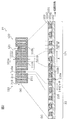
- FIG. 9B is a plan view schematically showing the electrode structure of the filter 20C in the application example 3 of the second embodiment.
- other circuit elements capacitor C1 and C2 and switches SW1 and SW2 that constitute the filter 20C together with the resonator are also schematically shown.
- the parallel arm resonator p1 and the parallel arm resonator p2 are arranged along the propagation direction of the elastic wave.
- positioning of the parallel arm resonator p1 and the parallel arm resonator p2 is not restricted to this, For example, you may arrange
- FIG. 9C is a graph showing characteristics of the filter 20C in the application example 3 of the second embodiment. Specifically, (a) and (b) in the figure show the impedance characteristics of the resonator alone, the combined characteristics of the parallel arm resonator p1 and the capacitor C1 ("p1 + C1 combined characteristics" in the figure), and the parallel characteristics.
- the parallel arm resonance circuit in this application example is a circuit provided in a path connecting the node x1 and the ground, and specifically, the parallel arm resonator p1, the capacitor C1, the switch SW1, and the parallel arm resonator p2. , Capacitor C2 and switch SW2.
- FIG. 6C is a graph showing the comparison of filter characteristics when both the switches SW1 and SW2 are on or off.
- the pass characteristics of the filter 20C have steep attenuation slopes on the high side of the passband and the low side of the passband. Shift to the high side while maintaining the characteristics.
- the filter 20C can switch the frequencies of the attenuation poles on the high side of the passband and the low side of the passband according to the switching of the conduction and non-conduction of the switches SW1 and WS2, and at the high end of the passband.
- an increase in insertion loss at the lower end of the passband can be suppressed. For this reason, for example, the filter 20C can switch the center frequency while maintaining the bandwidth.
- the switches SW1 and SW2 may not be switched on and off, or may be switched individually. However, when both of the switches SW1 and SW2 are switched on and off, the number of control lines for controlling the switches SW1 and SW2 can be reduced, so that the configuration of the filter 20C can be simplified.
- the high band end of the pass band can be varied according to the on / off state of the switch SW2 connected in series to the parallel arm resonator p2. Further, the low band end of the pass band can be varied according to the on / off state of the switch SW1 connected in series to the parallel arm resonator p1.
- both the switches SW1 and SW2 on or off, it is possible to shift both the low band end and high band end of the pass band to the low band side or the high band side. That is, the center frequency of the pass band can be shifted to the low frequency side or the high frequency side.
- both the low band end and high band end of the pass band are shifted so that these frequency differences are widened or narrowed. be able to. That is, the pass band width can be varied while making the center frequency of the pass band substantially constant.
- the other when one of the switches SW1 and SW2 is turned on or off, the other is turned on and off, so that one of the low band end and the high band end of the pass band is fixed and the other is connected to the low band side or the high band. Can be shifted to the side. That is, the low band end or high band end of the pass band can be varied.
- the stop band high band end of the parallel arm resonator p1 is the pass band. Easy to be located within. That is, in this case, if a ripple is generated at the high end of the stop band of the parallel arm resonator p1, the loss in the pass band can be increased. Therefore, in such a filter 20C, setting the IR pitch of the parallel arm resonator p1 to 0.42 ⁇ or more and less than 0.50 ⁇ is particularly useful from the viewpoint of suppressing loss in the passband.
- the filter has one impedance circuit that is a circuit in which a pair of impedance elements (for example, a capacitor) and a switch are connected in parallel, and at least one of the parallel arm resonators p1 and p2 is connected in series with the impedance circuit. It doesn't matter. Such a filter will be described using application examples 4 to 6.
- FIG. 10 is a circuit configuration diagram of a filter 20D in application example 4 of the second embodiment.
- the filter 20D shown in the figure is different from the filter 20C shown in FIG. 9A in that the parallel arm resonator p1 connects the node x1 and the ground without the capacitor C1 and the switch SW1. Further, the capacitor C and the switch SW shown in the figure correspond to the capacitor C2 and the switch SW2 shown in FIG. 9A. In other words, the filter 20D has an impedance circuit that is a circuit in which a pair of capacitors C and a switch SW are connected in parallel.
- the parallel arm resonator p2 (second parallel arm resonator) is connected in series with the impedance circuit, and the parallel arm resonator p1 (first parallel arm resonator) is connected to the parallel arm resonator p2 and the impedance circuit. Are connected in parallel to the circuit connected in series.
- the filter characteristic of the filter 20D in this application example corresponds to the characteristic when the switch SW1 is fixed on and the switch SW2 is turned on and off in the above application example 3. That is, the filter 20D has the first characteristic while suppressing the increase of the insertion loss at the high end of the pass band while switching the frequency of the attenuation pole on the high side of the pass band in accordance with the switching of the switch SW. And the second characteristic can be switched.
- FIG. 11 is a circuit configuration diagram of the filter 20E according to the application example 5 of the second embodiment.
- the filter 20E shown in the figure is different from the filter 20C shown in FIG. 9A in that the parallel arm resonator p2 does not have the capacitor C2 and the switch SW2, and the node x1 is connected to the ground. Further, the capacitor C and the switch SW shown in the figure correspond to the capacitor C1 and the switch SW1 shown in FIG. 9A. In other words, the filter 20E has an impedance circuit that is a circuit in which a pair of capacitors C and a switch SW are connected in parallel.
- the parallel arm resonator p1 (first parallel arm resonator) is connected in series with the impedance circuit, and the parallel arm resonator p2 (second parallel arm resonator) is connected to the parallel arm resonator p1 and the impedance circuit. Are connected in parallel to the circuit connected in series.
- the filter characteristic of the filter 20E in this application example corresponds to the characteristic when the switch SW2 is fixed on and the switch SW1 is turned on and off in the above application example 3.
- the filter 20E switches the first attenuation while suppressing the increase of the insertion loss at the low band end of the pass band while switching the frequency of the attenuation pole on the low band side according to the switching of the switch SW.
- the characteristic and the second characteristic can be switched.
- FIG. 12 is a circuit configuration diagram of a filter 20F in application example 6 of the second embodiment.
- the filter 20F shown in FIG. 10 includes a pair of capacitors C and a switch SW connected in parallel to each other, and the parallel arm resonator p1 and the parallel arm resonance.
- the difference is that the child p2 is connected in series to the circuit connected in parallel.
- an impedance circuit including the capacitor C and the switch SW is connected in series to a circuit in which the parallel arm resonator p1 and the parallel arm resonator p2 are connected in parallel.
- the filter 20F can switch both the frequencies of the poles (attenuation poles) on both sides of the passband in accordance with switching between conduction and non-conduction of the switch SW.
- the filter (elastic wave filter device) described in the first and second embodiments can be applied to a high-frequency front-end circuit or the like.
- FIG. 13 is a configuration diagram of the high-frequency front-end circuit 1 and its peripheral circuits according to the third embodiment.
- a high-frequency front-end circuit 1 an antenna element 2, and an RF signal processing circuit (RFIC) 3 are shown.
- the high-frequency front end circuit 1, the antenna element 2, and the RFIC 3 constitute a communication device 4.
- the antenna element 2, the high-frequency front end circuit 1, and the RFIC 3 are disposed, for example, in a front end portion of a mobile phone that supports multimode / multiband.
- the antenna element 2 is a multiband antenna that transmits and receives a high-frequency signal and conforms to a communication standard such as 3GPP (Third Generation Partnership Project).
- the antenna element 2 may not correspond to, for example, all the bands of the communication device 4, and may correspond to only the bands of the low frequency band group or the high frequency band group.
- the antenna element 2 is not built in the communication device 4 and may be provided separately from the communication device 4.
- RFIC 3 is an RF signal processing circuit that processes high-frequency signals transmitted and received by the antenna element 2. Specifically, the RFIC 3 performs signal processing on the high-frequency reception signal input from the antenna element 2 via the reception-side signal path of the high-frequency front-end circuit 1 by down-conversion or the like, and receives the signal generated by the signal processing. The signal is output to a baseband signal processing circuit (not shown). The RFIC 3 performs signal processing on the transmission signal input from the baseband signal processing circuit by up-conversion or the like, and transmits the high-frequency transmission signal generated by the signal processing to the transmission-side signal path (not shown) of the high-frequency front-end circuit 1. Output).
- the high frequency front end circuit 1 is a circuit that transmits a high frequency signal between the antenna element 2 and the RFIC 3. Specifically, the high frequency front end circuit 1 transmits the high frequency transmission signal output from the RFIC 3 to the antenna element 2 via a transmission side signal path (not shown). The high-frequency front end circuit 1 transmits a high-frequency reception signal received by the antenna element 2 to the RFIC 3 via the reception-side signal path.
- a configuration in which the filter according to Embodiments 1 and 2 is provided in the reception-side signal path of the high-frequency front-end circuit 1 will be described. May be provided.
- the high-frequency front-end circuit 1 includes, in order from the antenna element 2 side, switch groups 110A to 110C composed of a plurality of switches, a filter group 120 composed of a plurality of filters, a switch group 150, and a reception amplification circuit group 160. With.
- the switch groups 110A to 110C include one or more switches (in this embodiment, a plurality of switches) that connect the antenna element 2 and a signal path corresponding to a predetermined band in accordance with a control signal from a control unit (not shown). ).
- the number of signal paths connected to the antenna element 2 is not limited to one, and a plurality of signal paths may be used. That is, the high frequency front end circuit 1 may support carrier aggregation.
- the filter group 120 includes one or more filters, and in the present embodiment, for example, includes the following plurality of filters.
- the band includes (i) a tunable filter that can handle Bands 11, 21, and 32, (ii) a tunable filter that can handle CA (carrier aggregation) of Band3 and Band3 and 9, (Iii) a filter corresponding to Band 25, (iv) a filter corresponding to Band 34, (v) a filter corresponding to Band 1, 4, 65 and 66, (vi) a filter corresponding to Band 40, and (vii) a filter corresponding to Band 30. , (Viii) a filter corresponding to Band 41, and (ix) Band 7 and a tunable filter capable of supporting CAs of Band 7 and 38.
- Switch group 150 connects a signal path corresponding to a predetermined band and a reception amplifier circuit corresponding to the predetermined band in reception amplifier circuit group 160 in accordance with a control signal from a control unit (not shown). It is composed of one or more switches (a plurality of switches in this embodiment). The number of signal paths connected to the antenna element 2 is not limited to one, and a plurality of signal paths may be used. That is, the high frequency front end circuit 1 may support carrier aggregation. As a result, the high-frequency signal (here, the high-frequency reception signal) input from the antenna element 2 is amplified by the predetermined reception amplification circuit of the reception amplification circuit group 160 via the predetermined filter of the filter group 120, and is transmitted to the RFIC 3 Is output. Note that the RFIC corresponding to the low band and the RFIC corresponding to the high band may be provided separately.
- the reception amplifier circuit group 160 includes one or more low noise amplifiers (a plurality of low noise amplifiers in the present embodiment) that amplify the power of the high frequency reception signals input from the switch group 150.
- the thus configured high-frequency front-end circuit 1 includes any one of the filters 20A to 20F in the application example of the second embodiment as at least one tunable filter. According to this, since the number of filters can be reduced compared with the case where a filter is provided for each band, the size can be reduced.
- the high frequency front end circuit 1 may include the filter 10 according to the above-described embodiment as a filter having a fixed pass band.
- the communication device 4 including the above-described high-frequency front-end circuit and RFIC 3 (RF signal processing circuit) is also included in the present invention. According to such a communication device 4, it is possible to achieve low loss and high selectivity.
- a multiplexer such as a duplexer provided with the above-described filter is also included in the present invention. That is, in a multiplexer in which a plurality of filters are commonly connected, at least one filter may be any of the above-described filters.
- the series arm resonator s1 and the parallel arm resonator p2 are not limited to the elastic wave resonator using the surface acoustic wave, and may be configured by an elastic wave resonator using a bulk wave or a boundary acoustic wave, for example. It doesn't matter. That is, the series arm resonator s1 and the parallel arm resonator p2 may not be configured by the IDT electrode.
- the series arm resonator s1 and the parallel arm resonator p2 preferably have reflectors from the viewpoint of reducing loss, but for example, when there are restrictions on mounting layout, the series arm resonator s1 and the parallel arm resonator p2 may not have reflectors. It doesn't matter. That is, at least one of the series arm resonator s1 and the parallel arm resonator p2 is configured by only an IDT electrode without having one set of reflectors among an IDT electrode and a set of reflectors that constitute each. It does not matter.
- At least one of the series arm resonator s1 and the parallel arm resonators p1 and p2 may have only one of the reflectors arranged on both sides of the IDT electrode.
- an inductor or a capacitor may be connected between each component.
- the inductor may include a wiring inductor formed by wiring that connects the components.
- the present invention can be widely used as a low-loss filter, multiplexer, front-end circuit, and communication device for communication devices such as mobile phones.
Landscapes
- Physics & Mathematics (AREA)
- Acoustics & Sound (AREA)
- Engineering & Computer Science (AREA)
- Computer Networks & Wireless Communication (AREA)
- Signal Processing (AREA)
- Chemical & Material Sciences (AREA)
- Crystallography & Structural Chemistry (AREA)
- Surface Acoustic Wave Elements And Circuit Networks Thereof (AREA)
Abstract
Description
[1.フィルタの回路構成]
図1Aは、実施の形態1に係るフィルタ10の回路構成図である。
[2-1.電極構造]
次に、フィルタ10の構造について、説明する。
以下、フィルタ10を構成する各共振子の構造について、並列腕共振子p1に着目してより詳細に説明する。なお、他の共振子については、I-Rピッチが弾性波の波長λの0.5倍程度で構成されている点等を除き、並列腕共振子p1と概ね同じ構造を有するため、詳細な説明を省略する。
次に、本実施の形態に係るフィルタ10のフィルタ特性について、説明する。
一般的に、I-Rピッチは、弾性波の伝搬に規則性をもたせるためにIDT電極121の電極ピッチ(すなわち0.50λ)と同等に設計される。しかしながら、本願発明者は、1つの並列腕共振回路が複数の共振子を有する弾性波フィルタ装置において、このように設計された共振子を用いた場合、通過帯域内のロスが悪化(増大)し得るという問題に気付いた。
以下、本実施の形態に係るフィルタ10によって奏される効果について、実施例及び比較例に基づいて、詳細に説明する。
以上のように、本願発明者は、鋭意検討の結果、並列腕共振子p1(第1並列腕共振子)のI-Rピッチ(IDT電極121と反射器122とのピッチ)を0.42λ以上かつ0.50λ未満とすることにより、通過帯域内のロスを抑制できることを見出した。具体的には、I-Rピッチを大きくし過ぎると、並列腕共振子p1のストップバンド高域端のリップルが大きくなることにより、通過帯域内のロスが増大する。一方、I-Rピッチを小さくし過ぎると、並列腕共振子p1の共振周波数高域側のリップルが大きくなることにより、通過帯域内のロスが増大もしくは通過帯域低域側の減衰特性が悪化する。よって、並列腕共振子p1のI-Rピッチを適正範囲に収めることで、通過帯域内のロスを抑制することができる。
上記実施の形態1に係るフィルタ10(弾性波フィルタ装置)の構成は、通過帯域を可変できるチューナブルフィルタに適用することができる。そこで、実施の形態2に係るフィルタとして、このようなチューナブルフィルタについて適用例1~6を用いて説明する。具体的には、適用例1及び2は、上記実施の形態1に係るフィルタ10のチューナブルフィルタへの適用例である。また、適用例3~6は、上記実施の形態1における並列腕共振子p1(第1並列腕共振子)及び並列腕共振子p2(第2並列腕共振子)を並列接続した構成のチューナブルフィルタへの適用例である。
図7Aは、実施の形態2の適用例1におけるフィルタ20Aの回路構成図である。
図8Aは、実施の形態2の適用例2におけるフィルタ20Bの回路構成図である。
図9Aは、実施の形態2の適用例3におけるフィルタ20Cの回路構成図である。
図10は、実施の形態2の適用例4におけるフィルタ20Dの回路構成図である。
図11は、実施の形態2の適用例5におけるフィルタ20Eの回路構成図である。
図12は、実施の形態2の適用例6におけるフィルタ20Fの回路構成図である。
以上の実施の形態1及び2で説明したフィルタ(弾性波フィルタ装置)は、高周波フロントエンド回路等に適用することができる。
以上、本発明の実施の形態に係る弾性波フィルタ装置及び高周波フロントエンド回路について、実施の形態1~3を挙げて説明したが、本発明は、上記実施の形態に限定されるものではない。上記実施の形態における任意の構成要素を組み合わせて実現される別の実施の形態や、上記実施の形態に対して本発明の主旨を逸脱しない範囲で当業者が思いつく各種変形を施して得られる変形例や、本発明に係る弾性波フィルタ装置及び高周波フロントエンド回路を内蔵した各種機器も本発明に含まれる。
2 アンテナ素子
3 RFIC(RF信号処理回路)
4 通信装置
10、20A~20F フィルタ(弾性波フィルタ装置)
11m 入出力端子(第1入出力端子)
11n 入出力端子(第2入出力端子)
101 電極膜
101a、101b 櫛歯電極
101g 密着層
101h 主電極層
102 圧電基板
103 保護層
110a、110b、210 電極指
110A~110C、150 スイッチ群
111、121、131 IDT電極
111a、111b、211 バスバー電極
112、122、132 反射器
120 フィルタ群
160 受信増幅回路群
C、C1、C2 キャパシタ(インピーダンス素子)
L インダクタ(インピーダンス素子)
p1、p2 並列腕共振子
s1 直列腕共振子(直列腕共振回路)
SW、SW1、SW2 スイッチ(スイッチ素子)
Claims (10)
- 第1入出力端子と第2入出力端子とを結ぶ経路上に接続された1以上の弾性波共振子からなる直列腕共振回路と、
前記経路上の同一ノードとグランドとの間に接続された第1並列腕共振子及び第2並列腕共振子と、を有し、
前記第1並列腕共振子における共振周波数は、前記第2並列腕共振子における共振周波数よりも低く、
前記第1並列腕共振子における反共振周波数は、前記第2並列腕共振子における反共振周波数よりも低く、
前記第1並列腕共振子は、
弾性波共振子からなり、
弾性波を励振するIDT電極と、
前記IDT電極で励振された弾性波を反射する反射器と、を有し、
前記IDT電極の電極周期で定まる弾性波の波長をλとしたとき、前記IDT電極と前記反射器とのピッチが0.42λ以上かつ0.50λ未満である、
弾性波フィルタ装置。 - 前記第1並列腕共振子は、前記IDT電極と前記反射器とのピッチが0.44λ以上かつ0.46λ以下である、
請求項1に記載の弾性波フィルタ装置。 - さらに、一対のインピーダンス素子及びスイッチ素子が並列接続されたインピーダンス回路を有し、
前記第1並列腕共振子及び前記第2並列腕共振子のうち少なくとも一方は、前記インピーダンス回路と直列接続されている、
請求項1または2に記載の弾性波フィルタ装置。 - 前記第2並列腕共振子は、前記インピーダンス回路と直列接続され、
前記第1並列腕共振子は、前記第2並列腕共振子と前記インピーダンス回路とが直列接続された回路に対して並列接続されている、
請求項3に記載の弾性波フィルタ装置。 - 前記第1並列腕共振子は、前記インピーダンス回路と直列接続され、
前記第2並列腕共振子は、前記第1並列腕共振子と前記インピーダンス回路とが直列接続された回路に対して並列接続されている、
請求項3に記載の弾性波フィルタ装置。 - 前記第1並列腕共振子と前記第2並列腕共振子とは並列接続されており、
前記インピーダンス回路は、前記第1並列腕共振子と前記第2並列腕共振子とが並列接続された回路に対して直列接続されている、
請求項3に記載の弾性波フィルタ装置。 - さらに、一対のインピーダンス素子及びスイッチ素子が並列されたインピーダンス回路を2つ有し、
前記第1並列腕共振子は、2つの前記インピーダンス回路のうち一方のインピーダンス回路と直列接続され、
前記第2並列腕共振子は、2つの前記インピーダンス回路のうち他方のインピーダンス回路と直列接続され、
前記第1並列腕共振子と前記一方のインピーダンス回路とが直列接続された回路と、前記第2並列腕共振子と前記他方のインピーダンス回路とが直列接続された回路とは、並列接続されている、
請求項1または2に記載の弾性波フィルタ装置。 - さらに、前記第1並列腕共振子及び前記第2並列腕共振子の一方の並列腕共振子に並列接続されたスイッチ素子を有し、
前記第1並列腕共振子及び前記第2並列腕共振子の他方の並列腕共振子は、前記一方の並列腕共振子と前記スイッチ素子とが並列接続された回路に対して直列接続されている、
請求項1または2に記載の弾性波フィルタ装置。 - 請求項1~8のいずれか1項に記載の弾性波フィルタ装置と、
前記弾性波フィルタ装置に接続された増幅回路と、を備える、
高周波フロントエンド回路。 - アンテナ素子で送受信される高周波信号を処理するRF信号処理回路と、
前記アンテナ素子と前記RF信号処理回路との間で前記高周波信号を伝達する請求項9に記載の高周波フロントエンド回路と、を備える、
通信装置。
Priority Applications (4)
| Application Number | Priority Date | Filing Date | Title |
|---|---|---|---|
| KR1020197005756A KR102194752B1 (ko) | 2016-09-02 | 2017-08-30 | 탄성파 필터 장치, 고주파 프론트엔드 회로 및 통신 장치 |
| JP2018537369A JP6741069B2 (ja) | 2016-09-02 | 2017-08-30 | 弾性波フィルタ装置、高周波フロントエンド回路及び通信装置 |
| CN201780053333.2A CN109661777B (zh) | 2016-09-02 | 2017-08-30 | 弹性波滤波器装置、高频前端电路以及通信装置 |
| US16/283,865 US10630261B2 (en) | 2016-09-02 | 2019-02-25 | Acoustic wave filter device, radio-frequency front-end circuit, and communication apparatus |
Applications Claiming Priority (2)
| Application Number | Priority Date | Filing Date | Title |
|---|---|---|---|
| JP2016-172272 | 2016-09-02 | ||
| JP2016172272 | 2016-09-02 |
Related Child Applications (1)
| Application Number | Title | Priority Date | Filing Date |
|---|---|---|---|
| US16/283,865 Continuation US10630261B2 (en) | 2016-09-02 | 2019-02-25 | Acoustic wave filter device, radio-frequency front-end circuit, and communication apparatus |
Publications (1)
| Publication Number | Publication Date |
|---|---|
| WO2018043610A1 true WO2018043610A1 (ja) | 2018-03-08 |
Family
ID=61309451
Family Applications (1)
| Application Number | Title | Priority Date | Filing Date |
|---|---|---|---|
| PCT/JP2017/031271 Ceased WO2018043610A1 (ja) | 2016-09-02 | 2017-08-30 | 弾性波フィルタ装置、高周波フロントエンド回路及び通信装置 |
Country Status (5)
| Country | Link |
|---|---|
| US (1) | US10630261B2 (ja) |
| JP (1) | JP6741069B2 (ja) |
| KR (1) | KR102194752B1 (ja) |
| CN (1) | CN109661777B (ja) |
| WO (1) | WO2018043610A1 (ja) |
Cited By (4)
| Publication number | Priority date | Publication date | Assignee | Title |
|---|---|---|---|---|
| CN111384924A (zh) * | 2018-12-25 | 2020-07-07 | 株式会社村田制作所 | 多工器、高频前端电路以及通信装置 |
| JPWO2021006055A1 (ja) * | 2019-07-05 | 2021-01-14 | ||
| WO2021006056A1 (ja) * | 2019-07-05 | 2021-01-14 | 株式会社村田製作所 | 弾性波装置、高周波フロントエンド回路及び通信装置 |
| WO2023080142A1 (ja) * | 2021-11-08 | 2023-05-11 | 株式会社村田製作所 | フィルタデバイス |
Families Citing this family (6)
| Publication number | Priority date | Publication date | Assignee | Title |
|---|---|---|---|---|
| JP7215413B2 (ja) * | 2019-12-27 | 2023-01-31 | 株式会社村田製作所 | 弾性波フィルタ |
| KR102752483B1 (ko) * | 2020-01-20 | 2025-01-10 | 가부시키가이샤 무라타 세이사쿠쇼 | 필터 장치, 멀티플렉서, 고주파 프론트엔드 회로 및 통신 장치 |
| JP7468627B2 (ja) * | 2020-03-31 | 2024-04-16 | 株式会社村田製作所 | マルチプレクサ |
| CN115997343B (zh) * | 2020-09-02 | 2026-04-03 | 株式会社村田制作所 | 弹性波滤波器以及多工器 |
| KR20220123934A (ko) * | 2021-03-02 | 2022-09-13 | 삼성전기주식회사 | 음향 공진기 필터 |
| US20230353125A1 (en) * | 2022-04-29 | 2023-11-02 | Avago Technologies International Sales Pte. Limited | Switch-based variable acoustic resonator |
Citations (4)
| Publication number | Priority date | Publication date | Assignee | Title |
|---|---|---|---|---|
| JP2006013576A (ja) * | 2004-06-22 | 2006-01-12 | Epson Toyocom Corp | Sawデバイスとこれを用いた装置 |
| JP2009207116A (ja) * | 2008-01-31 | 2009-09-10 | Fujitsu Ltd | 弾性波デバイス、デュープレクサ、通信モジュール、および通信装置 |
| JP2014068123A (ja) * | 2012-09-25 | 2014-04-17 | Murata Mfg Co Ltd | ラダー型フィルタ及び分波器 |
| WO2016017730A1 (ja) * | 2014-07-30 | 2016-02-04 | 京セラ株式会社 | 弾性波素子、フィルタ素子および通信装置 |
Family Cites Families (6)
| Publication number | Priority date | Publication date | Assignee | Title |
|---|---|---|---|---|
| JP2000323961A (ja) * | 1999-03-10 | 2000-11-24 | Matsushita Electric Ind Co Ltd | 弾性表面波共振器を用いた帯域切替フィルタとそれを用いたアンテナ共用器 |
| EP2416496B1 (en) * | 2009-03-30 | 2019-05-01 | Murata Manufacturing Co., Ltd. | Elastic wave filter |
| CN103004085B (zh) * | 2011-06-23 | 2015-04-15 | 天工松下滤波方案日本有限公司 | 梯型弹性波滤波器及使用该弹性波滤波器的天线双工器 |
| JP6017868B2 (ja) * | 2011-11-04 | 2016-11-02 | 太陽誘電株式会社 | 分波器、フィルタ及び通信モジュール |
| JP6013829B2 (ja) * | 2012-08-17 | 2016-10-25 | 太陽誘電株式会社 | 弾性波フィルタ、デュプレクサ及びモジュール |
| CN110140296B (zh) * | 2016-12-28 | 2023-01-13 | 株式会社村田制作所 | 纵耦合谐振器型弹性波滤波器 |
-
2017
- 2017-08-30 KR KR1020197005756A patent/KR102194752B1/ko active Active
- 2017-08-30 WO PCT/JP2017/031271 patent/WO2018043610A1/ja not_active Ceased
- 2017-08-30 CN CN201780053333.2A patent/CN109661777B/zh active Active
- 2017-08-30 JP JP2018537369A patent/JP6741069B2/ja active Active
-
2019
- 2019-02-25 US US16/283,865 patent/US10630261B2/en active Active
Patent Citations (4)
| Publication number | Priority date | Publication date | Assignee | Title |
|---|---|---|---|---|
| JP2006013576A (ja) * | 2004-06-22 | 2006-01-12 | Epson Toyocom Corp | Sawデバイスとこれを用いた装置 |
| JP2009207116A (ja) * | 2008-01-31 | 2009-09-10 | Fujitsu Ltd | 弾性波デバイス、デュープレクサ、通信モジュール、および通信装置 |
| JP2014068123A (ja) * | 2012-09-25 | 2014-04-17 | Murata Mfg Co Ltd | ラダー型フィルタ及び分波器 |
| WO2016017730A1 (ja) * | 2014-07-30 | 2016-02-04 | 京セラ株式会社 | 弾性波素子、フィルタ素子および通信装置 |
Cited By (10)
| Publication number | Priority date | Publication date | Assignee | Title |
|---|---|---|---|---|
| CN111384924A (zh) * | 2018-12-25 | 2020-07-07 | 株式会社村田制作所 | 多工器、高频前端电路以及通信装置 |
| CN111384924B (zh) * | 2018-12-25 | 2023-07-25 | 株式会社村田制作所 | 多工器、高频前端电路以及通信装置 |
| JPWO2021006055A1 (ja) * | 2019-07-05 | 2021-01-14 | ||
| WO2021006055A1 (ja) * | 2019-07-05 | 2021-01-14 | 株式会社村田製作所 | 弾性波装置、高周波フロントエンド回路及び通信装置 |
| WO2021006056A1 (ja) * | 2019-07-05 | 2021-01-14 | 株式会社村田製作所 | 弾性波装置、高周波フロントエンド回路及び通信装置 |
| JPWO2021006056A1 (ja) * | 2019-07-05 | 2021-01-14 | ||
| US12009799B2 (en) | 2019-07-05 | 2024-06-11 | Murata Manufacturing Co., Ltd. | Acoustic wave device, high-frequency front-end circuit, and communication device |
| JP7510416B2 (ja) | 2019-07-05 | 2024-07-03 | 株式会社村田製作所 | 弾性波装置、高周波フロントエンド回路及び通信装置 |
| JP7510417B2 (ja) | 2019-07-05 | 2024-07-03 | 株式会社村田製作所 | 弾性波装置、高周波フロントエンド回路及び通信装置 |
| WO2023080142A1 (ja) * | 2021-11-08 | 2023-05-11 | 株式会社村田製作所 | フィルタデバイス |
Also Published As
| Publication number | Publication date |
|---|---|
| CN109661777B (zh) | 2023-05-16 |
| CN109661777A (zh) | 2019-04-19 |
| JPWO2018043610A1 (ja) | 2019-06-27 |
| US10630261B2 (en) | 2020-04-21 |
| KR20190034288A (ko) | 2019-04-01 |
| KR102194752B1 (ko) | 2020-12-23 |
| JP6741069B2 (ja) | 2020-08-19 |
| US20190190496A1 (en) | 2019-06-20 |
Similar Documents
| Publication | Publication Date | Title |
|---|---|---|
| JP6669262B2 (ja) | 弾性波フィルタ装置、高周波フロントエンド回路及び通信装置 | |
| JP6741069B2 (ja) | 弾性波フィルタ装置、高周波フロントエンド回路及び通信装置 | |
| JP6669263B2 (ja) | 弾性波フィルタ装置、高周波フロントエンド回路及び通信装置 | |
| JP6750676B2 (ja) | 高周波フィルタ回路、マルチプレクサ、高周波フロントエンド回路及び通信装置 | |
| WO2019021983A1 (ja) | 高周波フィルタ、マルチプレクサ、高周波フロントエンド回路および通信装置 | |
| US10944381B2 (en) | Acoustic wave filter device, multiplexer, radio-frequency front end circuit, and communication device | |
| WO2018097203A1 (ja) | 弾性波フィルタ装置、マルチプレクサ、高周波フロントエンド回路および通信装置 | |
| WO2019065274A1 (ja) | フィルタ装置、マルチプレクサ、高周波フロントエンド回路および通信装置 | |
| WO2018061878A1 (ja) | 弾性波装置、高周波フロントエンド回路および通信装置 | |
| WO2018016279A1 (ja) | 高周波フィルタ回路、マルチプレクサ、高周波フロントエンド回路及び通信装置 | |
| US10530335B2 (en) | Acoustic wave filter device, radio-frequency front-end circuit, and communication apparatus | |
| US11394368B2 (en) | Acoustic wave filter, multiplexer, radio frequency front-end circuit, and communication device | |
| WO2018061949A1 (ja) | 弾性波フィルタ装置、マルチプレクサ、高周波フロントエンド回路及び通信装置 | |
| WO2018052073A1 (ja) | 弾性波フィルタ装置、マルチプレクサ、高周波フロントエンド回路及び通信装置 | |
| KR102193508B1 (ko) | 탄성파 필터 장치, 고주파 프론트엔드 회로 및 통신 장치 | |
| WO2018056224A1 (ja) | 弾性波装置、高周波フロントエンド回路および通信装置 | |
| US8106725B2 (en) | Acoustic wave filter device | |
| WO2019117106A1 (ja) | フィルタ装置およびマルチプレクサ | |
| WO2018056056A1 (ja) | 弾性波装置、高周波フロントエンド回路および通信装置 |
Legal Events
| Date | Code | Title | Description |
|---|---|---|---|
| 121 | Ep: the epo has been informed by wipo that ep was designated in this application |
Ref document number: 17846614 Country of ref document: EP Kind code of ref document: A1 |
|
| ENP | Entry into the national phase |
Ref document number: 20197005756 Country of ref document: KR Kind code of ref document: A |
|
| ENP | Entry into the national phase |
Ref document number: 2018537369 Country of ref document: JP Kind code of ref document: A |
|
| NENP | Non-entry into the national phase |
Ref country code: DE |
|
| 122 | Ep: pct application non-entry in european phase |
Ref document number: 17846614 Country of ref document: EP Kind code of ref document: A1 |