WO2018042754A1 - プラズマ原子層成長装置および原子層成長方法 - Google Patents
プラズマ原子層成長装置および原子層成長方法 Download PDFInfo
- Publication number
- WO2018042754A1 WO2018042754A1 PCT/JP2017/016187 JP2017016187W WO2018042754A1 WO 2018042754 A1 WO2018042754 A1 WO 2018042754A1 JP 2017016187 W JP2017016187 W JP 2017016187W WO 2018042754 A1 WO2018042754 A1 WO 2018042754A1
- Authority
- WO
- WIPO (PCT)
- Prior art keywords
- atomic layer
- layer growth
- growth apparatus
- film
- inert gas
- Prior art date
- Legal status (The legal status is an assumption and is not a legal conclusion. Google has not performed a legal analysis and makes no representation as to the accuracy of the status listed.)
- Ceased
Links
Images



Classifications
-
- H—ELECTRICITY
- H01—ELECTRIC ELEMENTS
- H01J—ELECTRIC DISCHARGE TUBES OR DISCHARGE LAMPS
- H01J37/00—Discharge tubes with provision for introducing objects or material to be exposed to the discharge, e.g. for the purpose of examination or processing thereof
- H01J37/32—Gas-filled discharge tubes
- H01J37/32009—Arrangements for generation of plasma specially adapted for examination or treatment of objects, e.g. plasma sources
- H01J37/32082—Radio frequency generated discharge
- H01J37/32091—Radio frequency generated discharge the radio frequency energy being capacitively coupled to the plasma
-
- C—CHEMISTRY; METALLURGY
- C23—COATING METALLIC MATERIAL; COATING MATERIAL WITH METALLIC MATERIAL; CHEMICAL SURFACE TREATMENT; DIFFUSION TREATMENT OF METALLIC MATERIAL; COATING BY VACUUM EVAPORATION, BY SPUTTERING, BY ION IMPLANTATION OR BY CHEMICAL VAPOUR DEPOSITION, IN GENERAL; INHIBITING CORROSION OF METALLIC MATERIAL OR INCRUSTATION IN GENERAL
- C23C—COATING METALLIC MATERIAL; COATING MATERIAL WITH METALLIC MATERIAL; SURFACE TREATMENT OF METALLIC MATERIAL BY DIFFUSION INTO THE SURFACE, BY CHEMICAL CONVERSION OR SUBSTITUTION; COATING BY VACUUM EVAPORATION, BY SPUTTERING, BY ION IMPLANTATION OR BY CHEMICAL VAPOUR DEPOSITION, IN GENERAL
- C23C16/00—Chemical coating by decomposition of gaseous compounds, without leaving reaction products of surface material in the coating, i.e. chemical vapour deposition [CVD] processes
- C23C16/44—Chemical coating by decomposition of gaseous compounds, without leaving reaction products of surface material in the coating, i.e. chemical vapour deposition [CVD] processes characterised by the method of coating
-
- C—CHEMISTRY; METALLURGY
- C23—COATING METALLIC MATERIAL; COATING MATERIAL WITH METALLIC MATERIAL; CHEMICAL SURFACE TREATMENT; DIFFUSION TREATMENT OF METALLIC MATERIAL; COATING BY VACUUM EVAPORATION, BY SPUTTERING, BY ION IMPLANTATION OR BY CHEMICAL VAPOUR DEPOSITION, IN GENERAL; INHIBITING CORROSION OF METALLIC MATERIAL OR INCRUSTATION IN GENERAL
- C23C—COATING METALLIC MATERIAL; COATING MATERIAL WITH METALLIC MATERIAL; SURFACE TREATMENT OF METALLIC MATERIAL BY DIFFUSION INTO THE SURFACE, BY CHEMICAL CONVERSION OR SUBSTITUTION; COATING BY VACUUM EVAPORATION, BY SPUTTERING, BY ION IMPLANTATION OR BY CHEMICAL VAPOUR DEPOSITION, IN GENERAL
- C23C16/00—Chemical coating by decomposition of gaseous compounds, without leaving reaction products of surface material in the coating, i.e. chemical vapour deposition [CVD] processes
- C23C16/44—Chemical coating by decomposition of gaseous compounds, without leaving reaction products of surface material in the coating, i.e. chemical vapour deposition [CVD] processes characterised by the method of coating
- C23C16/4401—Means for minimising impurities, e.g. dust, moisture or residual gas, in the reaction chamber
-
- C—CHEMISTRY; METALLURGY
- C23—COATING METALLIC MATERIAL; COATING MATERIAL WITH METALLIC MATERIAL; CHEMICAL SURFACE TREATMENT; DIFFUSION TREATMENT OF METALLIC MATERIAL; COATING BY VACUUM EVAPORATION, BY SPUTTERING, BY ION IMPLANTATION OR BY CHEMICAL VAPOUR DEPOSITION, IN GENERAL; INHIBITING CORROSION OF METALLIC MATERIAL OR INCRUSTATION IN GENERAL
- C23C—COATING METALLIC MATERIAL; COATING MATERIAL WITH METALLIC MATERIAL; SURFACE TREATMENT OF METALLIC MATERIAL BY DIFFUSION INTO THE SURFACE, BY CHEMICAL CONVERSION OR SUBSTITUTION; COATING BY VACUUM EVAPORATION, BY SPUTTERING, BY ION IMPLANTATION OR BY CHEMICAL VAPOUR DEPOSITION, IN GENERAL
- C23C16/00—Chemical coating by decomposition of gaseous compounds, without leaving reaction products of surface material in the coating, i.e. chemical vapour deposition [CVD] processes
- C23C16/44—Chemical coating by decomposition of gaseous compounds, without leaving reaction products of surface material in the coating, i.e. chemical vapour deposition [CVD] processes characterised by the method of coating
- C23C16/455—Chemical coating by decomposition of gaseous compounds, without leaving reaction products of surface material in the coating, i.e. chemical vapour deposition [CVD] processes characterised by the method of coating characterised by the method used for introducing gases into reaction chamber or for modifying gas flows in reaction chamber
-
- C—CHEMISTRY; METALLURGY
- C23—COATING METALLIC MATERIAL; COATING MATERIAL WITH METALLIC MATERIAL; CHEMICAL SURFACE TREATMENT; DIFFUSION TREATMENT OF METALLIC MATERIAL; COATING BY VACUUM EVAPORATION, BY SPUTTERING, BY ION IMPLANTATION OR BY CHEMICAL VAPOUR DEPOSITION, IN GENERAL; INHIBITING CORROSION OF METALLIC MATERIAL OR INCRUSTATION IN GENERAL
- C23C—COATING METALLIC MATERIAL; COATING MATERIAL WITH METALLIC MATERIAL; SURFACE TREATMENT OF METALLIC MATERIAL BY DIFFUSION INTO THE SURFACE, BY CHEMICAL CONVERSION OR SUBSTITUTION; COATING BY VACUUM EVAPORATION, BY SPUTTERING, BY ION IMPLANTATION OR BY CHEMICAL VAPOUR DEPOSITION, IN GENERAL
- C23C16/00—Chemical coating by decomposition of gaseous compounds, without leaving reaction products of surface material in the coating, i.e. chemical vapour deposition [CVD] processes
- C23C16/44—Chemical coating by decomposition of gaseous compounds, without leaving reaction products of surface material in the coating, i.e. chemical vapour deposition [CVD] processes characterised by the method of coating
- C23C16/455—Chemical coating by decomposition of gaseous compounds, without leaving reaction products of surface material in the coating, i.e. chemical vapour deposition [CVD] processes characterised by the method of coating characterised by the method used for introducing gases into reaction chamber or for modifying gas flows in reaction chamber
- C23C16/45523—Pulsed gas flow or change of composition over time
- C23C16/45525—Atomic layer deposition [ALD]
- C23C16/45527—Atomic layer deposition [ALD] characterized by the ALD cycle, e.g. different flows or temperatures during half-reactions, unusual pulsing sequence, use of precursor mixtures or auxiliary reactants or activations
- C23C16/45536—Use of plasma, radiation or electromagnetic fields
-
- C—CHEMISTRY; METALLURGY
- C23—COATING METALLIC MATERIAL; COATING MATERIAL WITH METALLIC MATERIAL; CHEMICAL SURFACE TREATMENT; DIFFUSION TREATMENT OF METALLIC MATERIAL; COATING BY VACUUM EVAPORATION, BY SPUTTERING, BY ION IMPLANTATION OR BY CHEMICAL VAPOUR DEPOSITION, IN GENERAL; INHIBITING CORROSION OF METALLIC MATERIAL OR INCRUSTATION IN GENERAL
- C23C—COATING METALLIC MATERIAL; COATING MATERIAL WITH METALLIC MATERIAL; SURFACE TREATMENT OF METALLIC MATERIAL BY DIFFUSION INTO THE SURFACE, BY CHEMICAL CONVERSION OR SUBSTITUTION; COATING BY VACUUM EVAPORATION, BY SPUTTERING, BY ION IMPLANTATION OR BY CHEMICAL VAPOUR DEPOSITION, IN GENERAL
- C23C16/00—Chemical coating by decomposition of gaseous compounds, without leaving reaction products of surface material in the coating, i.e. chemical vapour deposition [CVD] processes
- C23C16/44—Chemical coating by decomposition of gaseous compounds, without leaving reaction products of surface material in the coating, i.e. chemical vapour deposition [CVD] processes characterised by the method of coating
- C23C16/455—Chemical coating by decomposition of gaseous compounds, without leaving reaction products of surface material in the coating, i.e. chemical vapour deposition [CVD] processes characterised by the method of coating characterised by the method used for introducing gases into reaction chamber or for modifying gas flows in reaction chamber
- C23C16/45523—Pulsed gas flow or change of composition over time
- C23C16/45525—Atomic layer deposition [ALD]
- C23C16/45544—Atomic layer deposition [ALD] characterized by the apparatus
-
- C—CHEMISTRY; METALLURGY
- C23—COATING METALLIC MATERIAL; COATING MATERIAL WITH METALLIC MATERIAL; CHEMICAL SURFACE TREATMENT; DIFFUSION TREATMENT OF METALLIC MATERIAL; COATING BY VACUUM EVAPORATION, BY SPUTTERING, BY ION IMPLANTATION OR BY CHEMICAL VAPOUR DEPOSITION, IN GENERAL; INHIBITING CORROSION OF METALLIC MATERIAL OR INCRUSTATION IN GENERAL
- C23C—COATING METALLIC MATERIAL; COATING MATERIAL WITH METALLIC MATERIAL; SURFACE TREATMENT OF METALLIC MATERIAL BY DIFFUSION INTO THE SURFACE, BY CHEMICAL CONVERSION OR SUBSTITUTION; COATING BY VACUUM EVAPORATION, BY SPUTTERING, BY ION IMPLANTATION OR BY CHEMICAL VAPOUR DEPOSITION, IN GENERAL
- C23C16/00—Chemical coating by decomposition of gaseous compounds, without leaving reaction products of surface material in the coating, i.e. chemical vapour deposition [CVD] processes
- C23C16/44—Chemical coating by decomposition of gaseous compounds, without leaving reaction products of surface material in the coating, i.e. chemical vapour deposition [CVD] processes characterised by the method of coating
- C23C16/455—Chemical coating by decomposition of gaseous compounds, without leaving reaction products of surface material in the coating, i.e. chemical vapour deposition [CVD] processes characterised by the method of coating characterised by the method used for introducing gases into reaction chamber or for modifying gas flows in reaction chamber
- C23C16/45563—Gas nozzles
-
- C—CHEMISTRY; METALLURGY
- C23—COATING METALLIC MATERIAL; COATING MATERIAL WITH METALLIC MATERIAL; CHEMICAL SURFACE TREATMENT; DIFFUSION TREATMENT OF METALLIC MATERIAL; COATING BY VACUUM EVAPORATION, BY SPUTTERING, BY ION IMPLANTATION OR BY CHEMICAL VAPOUR DEPOSITION, IN GENERAL; INHIBITING CORROSION OF METALLIC MATERIAL OR INCRUSTATION IN GENERAL
- C23C—COATING METALLIC MATERIAL; COATING MATERIAL WITH METALLIC MATERIAL; SURFACE TREATMENT OF METALLIC MATERIAL BY DIFFUSION INTO THE SURFACE, BY CHEMICAL CONVERSION OR SUBSTITUTION; COATING BY VACUUM EVAPORATION, BY SPUTTERING, BY ION IMPLANTATION OR BY CHEMICAL VAPOUR DEPOSITION, IN GENERAL
- C23C16/00—Chemical coating by decomposition of gaseous compounds, without leaving reaction products of surface material in the coating, i.e. chemical vapour deposition [CVD] processes
- C23C16/44—Chemical coating by decomposition of gaseous compounds, without leaving reaction products of surface material in the coating, i.e. chemical vapour deposition [CVD] processes characterised by the method of coating
- C23C16/50—Chemical coating by decomposition of gaseous compounds, without leaving reaction products of surface material in the coating, i.e. chemical vapour deposition [CVD] processes characterised by the method of coating using electric discharges
- C23C16/505—Chemical coating by decomposition of gaseous compounds, without leaving reaction products of surface material in the coating, i.e. chemical vapour deposition [CVD] processes characterised by the method of coating using electric discharges using radio frequency discharges
- C23C16/509—Chemical coating by decomposition of gaseous compounds, without leaving reaction products of surface material in the coating, i.e. chemical vapour deposition [CVD] processes characterised by the method of coating using electric discharges using radio frequency discharges using internal electrodes
- C23C16/5096—Flat-bed apparatus
-
- H—ELECTRICITY
- H01—ELECTRIC ELEMENTS
- H01J—ELECTRIC DISCHARGE TUBES OR DISCHARGE LAMPS
- H01J37/00—Discharge tubes with provision for introducing objects or material to be exposed to the discharge, e.g. for the purpose of examination or processing thereof
- H01J37/32—Gas-filled discharge tubes
- H01J37/32431—Constructional details of the reactor
- H01J37/3244—Gas supply means
- H01J37/32449—Gas control, e.g. control of the gas flow
-
- H—ELECTRICITY
- H01—ELECTRIC ELEMENTS
- H01J—ELECTRIC DISCHARGE TUBES OR DISCHARGE LAMPS
- H01J37/00—Discharge tubes with provision for introducing objects or material to be exposed to the discharge, e.g. for the purpose of examination or processing thereof
- H01J37/32—Gas-filled discharge tubes
- H01J37/32431—Constructional details of the reactor
- H01J37/32458—Vessel
- H01J37/32477—Vessel characterised by the means for protecting vessels or internal parts, e.g. coatings
-
- H—ELECTRICITY
- H01—ELECTRIC ELEMENTS
- H01J—ELECTRIC DISCHARGE TUBES OR DISCHARGE LAMPS
- H01J37/00—Discharge tubes with provision for introducing objects or material to be exposed to the discharge, e.g. for the purpose of examination or processing thereof
- H01J37/32—Gas-filled discharge tubes
- H01J37/32431—Constructional details of the reactor
- H01J37/32532—Electrodes
- H01J37/32559—Protection means, e.g. coatings
-
- H—ELECTRICITY
- H10—SEMICONDUCTOR DEVICES; ELECTRIC SOLID-STATE DEVICES NOT OTHERWISE PROVIDED FOR
- H10K—ORGANIC ELECTRIC SOLID-STATE DEVICES
- H10K50/00—Organic light-emitting devices
- H10K50/10—OLEDs or polymer light-emitting diodes [PLED]
- H10K50/11—OLEDs or polymer light-emitting diodes [PLED] characterised by the electroluminescent [EL] layers
-
- H—ELECTRICITY
- H10—SEMICONDUCTOR DEVICES; ELECTRIC SOLID-STATE DEVICES NOT OTHERWISE PROVIDED FOR
- H10P—GENERIC PROCESSES OR APPARATUS FOR THE MANUFACTURE OR TREATMENT OF DEVICES COVERED BY CLASS H10
- H10P14/00—Formation of materials, e.g. in the shape of layers or pillars
- H10P14/60—Formation of materials, e.g. in the shape of layers or pillars of insulating materials
-
- H—ELECTRICITY
- H01—ELECTRIC ELEMENTS
- H01J—ELECTRIC DISCHARGE TUBES OR DISCHARGE LAMPS
- H01J2237/00—Discharge tubes exposing object to beam, e.g. for analysis treatment, etching, imaging
- H01J2237/32—Processing objects by plasma generation
- H01J2237/33—Processing objects by plasma generation characterised by the type of processing
- H01J2237/332—Coating
Definitions
- the present invention relates to an atomic layer growth technique.
- Patent Document 1 uses a deposition plate in a film forming apparatus using a CVD method (Chemical Vapor Deposition) or a sputtering method, and deposits deposited on the inner wall of a chamber. A technique for covering with an amorphous film is described.
- CVD method Chemical Vapor Deposition
- sputtering method a technique for covering with an amorphous film is described.
- Patent Document 2 a plurality of deposition preventing plates are arranged corresponding to a plurality of side surface portions in a film forming chamber, and the deposition preventing plates are divided into a plurality of pieces so as to be close to each other. A technique for providing a gap between the protective plates is described.
- Patent Document 3 based on the pressure value of the sputtering space, the gas flow rate introduced into the sputtering space and the space between the inner wall of the vacuum chamber and the deposition plate are introduced. A technique for controlling a flow rate ratio with a gas flow rate is described.
- Patent Document 4 describes a technology in which a pair of deposition preventing plates formed with a plurality of through holes are arranged close to the inner wall of a processing chamber.
- Patent Document 5 describes a technique of attaching an adhesion preventing member for preventing adhesion of a film to the surface of a substrate carrier on the bottom surface of the substrate carrier.
- the atomic layer growth method is a film forming method for forming a film in units of atomic layers on a substrate by alternately supplying a source gas and a reaction gas onto the substrate.
- This atomic layer growth method has an advantage that it is excellent in step coverage and film thickness controllability because a film is formed in units of atomic layers.
- a film can be easily formed in a place that is difficult to remove without changing the film formation conditions. Easy to form. Therefore, in the atomic layer growth apparatus, the film quality of the film formed on the substrate due to the generation of foreign matters due to the peeling of the film formed in a place that is difficult to remove without changing the film forming conditions There is concern about deterioration.
- an atomic layer growth apparatus generates plasma discharge between a first electrode that holds a substrate and a second electrode that is disposed opposite to the first electrode, so that an atomic layer unit is formed on the substrate.
- An atomic layer growth apparatus for forming a film comprising an adhesion preventing member made of an insulator that surrounds and separates the second electrode in plan view.
- the film quality of the film formed on the substrate can be improved.
- a source gas used in a plasma CVD apparatus a source gas having a property of being difficult to diffuse to localize in the discharge space is used, and active species are generated from a plurality of source gases by plasma discharge. This is because the film material is formed only when (radical) is generated. Therefore, in the plasma CVD apparatus, a film tends not to be formed in a place away from the discharge space (a place where plasma discharge does not occur).
- a source gas and a reactive gas are alternately supplied between a lower electrode holding a substrate and an upper electrode disposed opposite to the lower electrode, and a reaction is performed.
- a film is formed on the substrate in units of atomic layers by performing plasma discharge when supplying the gas.
- a film having excellent step coverage can be formed by forming a film in units of atomic layers.
- a material that is easy to diffuse is used as the source gas, and each gas (source gas, purge gas, and reactive gas) is sufficiently contained in the film formation container.
- Each gas is alternately supplied while ensuring a sufficient time for diffusion.
- the source gas and the reaction gas are distributed not only on the substrate but also every corner of the film formation container.
- active species are formed by plasma discharge of the reactive gas, and the active species and the source gas adsorbed on the substrate react to form a film.
- the source gas and the reactive gas tend to react easily. Therefore, in the plasma atomic layer growth apparatus, the raw material gas and the reactive gas react to form a film even in a minute gap in the film forming container where no plasma discharge occurs.
- a film is formed in units of atomic layers, (2) a source gas or a reactive gas is distributed to every corner of the film formation container, and (3) a place where no plasma discharge occurs.
- a film is also formed in a minute gap.
- the plasma atomic layer growth apparatus has a property that a film is formed not only on the substrate but also every corner of the film formation container including the minute gap. Since the present inventors have found that there is room for improvement specific to the plasma atomic layer growth apparatus due to this property, the room for improvement will be described below.
- the upper electrode is supported by an insulating support member, for example.
- a film is formed to every corner of the film formation container, and thus a film is also formed on the insulating support member.
- a part of the adhering film peels off from the insulating support member and becomes a foreign substance. This foreign matter becomes a factor that degrades the quality of the film formed on the substrate. Therefore, in order to improve the film quality (quality) of the film formed on the substrate, it is necessary to remove the film attached to the insulating support member.
- an aluminum oxide film (Al 2 O 3 film) can be given as an example of a film formed by a plasma atomic layer growth apparatus, but this aluminum oxide film is difficult to remove by dry etching. is there. Therefore, in the plasma atomic layer growth apparatus, it is difficult to remove the film formed to every corner of the film formation container by dry etching using a cleaning gas. For example, a film attached to an insulating support member It is difficult to use dry etching for removing the film.
- the film forming conditions to be changed will change.
- the quality of the film formed on the substrate may vary.
- the film attached to the insulating support member that supports the upper electrode is improved without changing the film formation conditions, while improving the film quality of the film formed on the substrate. It can be seen that it is difficult to remove. Therefore, in this embodiment, a device for removing the film attached to the insulating support member that supports the upper electrode is taken. Below, the technical idea in this Embodiment which gave this device is demonstrated.
- FIG. 1 is a cross-sectional view schematically showing the overall configuration of plasma atomic layer growth apparatus 100 in the present embodiment.
- Plasma atomic layer growth apparatus 100 in the present embodiment is configured to form a film in units of atomic layers on substrate 1S by alternately supplying a source gas and a reactive gas. At that time, the substrate 1S can be heated to increase the reaction activity.
- TMA Tri-Methyl-Aluminum
- parallel plate electrodes are used to perform plasma discharge.
- the plasma atomic layer growth apparatus 100 in the present embodiment has a film formation container CB.
- a stage for holding the substrate 1S is disposed in the film formation container CB, and this stage functions as the lower electrode BE. Further, the stage includes a heater and is configured to be able to adjust the temperature of the substrate 1S. For example, in the case of plasma atomic layer growth apparatus 100 in the present embodiment, substrate 1S held on the stage is heated to 50 ° C. to 200 ° C.
- the film formation container CB is maintained in a vacuum.
- the film forming container CB is provided with a gas supply unit GSU for supplying a source gas, a purge gas, and a reactive gas, and a gas exhaust for exhausting the source gas, the purge gas, and the reactive gas.
- a gas supply unit GSU for supplying a source gas, a purge gas, and a reactive gas
- a gas exhaust for exhausting the source gas, the purge gas, and the reactive gas.
- Part GVU is provided.
- the gas supply unit GSU and the gas exhaust unit GVU are provided at positions facing each other, and the gas supplied from the gas supply unit GSU passes through the discharge space SP in the film formation container CB and is exhausted from the gas. Exhaust from part GVU.
- the upper electrode UE is disposed in the film formation container CB with a discharge space located above the substrate 1S mounted on the lower electrode BE interposed therebetween. That is, the upper electrode UE is disposed so as to face the lower electrode BE on which the substrate 1S is mounted.
- a top plate CT is disposed above the upper electrode UE, and a top plate support portion CTSP for supporting the upper electrode UE is provided on the top plate CT.
- an insulating support member ISM is disposed so as to be in close contact with the top plate support portion CTSP, and the upper electrode UE is supported by the insulating support member ISM. As shown in FIG.
- the plasma atomic layer growth apparatus 100 has an adhesion-preventing member CTM made of an insulator that surrounds the upper electrode UE in a plan view.
- the adhesion preventing member CTM is disposed so as to overlap the insulating support member ISM.
- the top plate CT is provided with an inert gas supply unit IGSU for supplying an inert gas such as nitrogen gas into the film formation container CB.
- an inert gas supply unit IGSU for supplying an inert gas such as nitrogen gas into the film formation container CB.
- the inert gas supply unit IGSU that supplies the inert gas is separately provided. Is provided.
- FIG. 2 is a diagram schematically showing a configuration of the deposition preventing member CTM in the present embodiment provided so as to surround and surround the upper electrode UE.
- a rectangular parallelepiped indicated by a two-dot chain line indicates a schematic configuration of the upper electrode UE.
- the upper electrode UE shown in FIG. 2 includes a surface SUR that faces the lower electrode BE shown in FIG. 1, a side surface SS1 that intersects the surface SUR, a side surface SS2 that is opposite to the side surface SS1, a surface SUR and a side surface SS1.
- the deposition preventing member CTM in the present embodiment is configured to surround and surround the upper electrode UE.
- the adhesion preventing member CTM in the present embodiment includes a part PT1 facing the side surface SS1 of the upper electrode UE, a part PT2 facing the side surface SS2 of the upper electrode UE, and a side surface SS3 of the upper electrode UE. And a portion PT4 facing the side surface SS4 of the upper electrode UE.
- the adhesion preventing member CTM in the present embodiment has an opening formed at the bottom of the adhesion preventing member CTM so as to expose the surface SUR of the upper electrode UE.
- each of the parts PT1 to PT4 of the deposition preventing member CTM in the present embodiment has an L shape having a horizontal part and a vertical part.
- a plurality of fixing holes SH for embedding the fixing member and a plurality of convex portions SU for supporting the fixing member are formed in each of the parts PT1 to PT4 of the adhesion preventing member CTM.
- the adhesion preventing member CTM is supported by the fixing member not shown in FIG.
- the plasma atomic layer growth apparatus according to the present embodiment is provided with the adhesion preventing member CTM surrounding the upper electrode UE.
- FIG. 3 is a schematic diagram showing an example of a configuration aspect of the deposition preventing member CTM in the present embodiment.
- the portions PT1 to PT4 constituting the deposition preventing member CTM are integrally formed. That is, the parts PT1 to PT4 of the adhesion preventing member CTM shown in FIG. 3 are formed as a seamless integral.
- a film is formed even in a place where a plasma discharge away from the discharge space is not generated, and Due to the film formation in units of layers, there is a property that a film is formed up to a minute gap. For this reason, in the plasma atomic layer growth apparatus, for example, a film also adheres to the deposition preventing member CTM that covers the upper electrode.
- the portions PT1 to PT4 of the adhesion-preventing member CTM shown in FIG. 3 are formed as a seamless integral. Therefore, in the adhesion preventing member CTM shown in FIG.
- the adhesion preventing member CTM formed as a seamless integral is a desirable member in which the generation source of the foreign matter is omitted as much as possible. This is because, as shown in FIG.
- the deposition preventing member CTM is constituted by a seamless integral
- the plasma atomic layer growth apparatus has a property that a film is easily formed in a fine gap as compared with a flat surface. For this reason, according to the adhesion-preventing member CTM made of a seamless integral body, there is no fine gap at which a film is easily formed, so that an advantage that the maintenance cycle of the adhesion-preventing member CTM can be extended can be obtained. .
- FIG. 4 is a schematic diagram showing another configuration example of the adhesion preventing member CTM in the present embodiment.
- the portions PT1 to PT4 constituting the adhesion-preventing member CTM are composed of separate pieces. That is, the adhesion-preventing member CTM shown in FIG. 4 is composed of a part PCE1 corresponding to the part PT1, a part PCE2 corresponding to the part PT2, a part PCE3 corresponding to the part PT3, and a part PCE4 corresponding to the part PT4. ing.
- the adhesion preventing member CTM in the present embodiment can be configured not only as a seamless integrated body shown in FIG. 3, but also as a combination of different parts shown in FIG.
- the adhesion preventing member CTM shown in FIG. 4 is also composed of a combination of different parts, there is a seam between the parts. For this reason, in the adhesion preventing member CTM shown in FIG. 4, there are fine gaps between components, and a film is also formed in the fine gaps. As a result, in the adhesion preventing member CTM shown in FIG. 4, it is considered that the generation potential of the foreign matter resulting from the peeling of the film formed in the minute gap is increased.
- the adhesion preventing member CTM When the adhesion preventing member CTM is formed from a combination of different parts, a fine gap is surely formed at the seam between the parts. Therefore, the generation potential of the foreign matter due to peeling of the film formed in the fine gap is small. It is thought to grow.
- the adhesion preventing member CTM when the adhesion preventing member CTM is composed of a combination of different parts, the adhesion preventing member CTM can be disassembled into respective parts and removed. When disassembled into individual parts in this way, there are no fine gaps that occur when the parts are combined, and by wet etching the individual parts, the film attached to the part corresponding to the fine gaps Can be removed.
- the adhesion preventing member CTM when the adhesion preventing member CTM is composed of a combination of different parts, a minute gap exists at the stage of combination, but the adhesion preventing member CTM can be disassembled and removed. For this reason, by performing wet etching on each disassembled component, it is possible to sufficiently remove even the film adhering to the site of each component corresponding to the minute gap.
- the adhesion preventing member CTM when the adhesion preventing member CTM is composed of a combination of different parts, the adhesion preventing member CTM having a low generation potential of foreign matter can be realized by disassembling and performing wet etching after being removed.
- the attachment shape and attachment position of the adhesion preventing member CTM before disassembly may be slightly different from the attachment shape and attachment position of the adhesion preventing member CTM after disassembly.
- the adhesion preventing member CTM itself is not a part directly related to plasma discharge like the upper electrode and the lower electrode, the attachment shape and attachment position of the adhesion preventing member CTM are delicate before and after disassembly.
- the adhesion preventing member CTM made of a seamless integral shown in FIG. 3 is desirable, while the adhesion preventing member made of a combination of different parts shown in FIG. CTM can also prevent foreign matter from adhering to the substrate, so that the quality (quality) of the film formed on the substrate can be improved.
- the plasma atomic layer growth apparatus has a property that a film is easily formed in a fine gap as compared with a flat surface. From this, when the adhesion preventing member CTM is constituted by a combination of different parts, the foreign matter is reduced by the amount of the minute gap where the film is easily formed as compared with the case where the adhesion preventing member CTM is constituted by a seamless integral. The generation potential of becomes higher. As a result, the maintenance cycle of the deposition preventing member CTM is shortened.
- the case where the adhesion preventing member CTM is constituted by a seamless one is more desirable than the case where the adhesion preventing member CTM is constituted by a combination of different parts.
- the adhesion preventing member CTM when the adhesion preventing member CTM is composed of a combination of different parts, there is a useful aspect in that the following advantages can be obtained.
- a fine gap is formed at the joint between the components. For example, when the deposition member CTM is heated in the film forming container, each of the components expands in volume. Even if it exists, as a result of being able to absorb this volume expansion with the fine clearance gap between components, a deformation
- the second advantage is that, for example, as the size of the upper electrode increases as the size of the plasma atomic layer growth apparatus increases, the size of the deposition preventing member CTM surrounding the upper electrode increases. Even if it exists, as a result of having comprised the adhesion prevention member CTM from several separate parts, the manufacture ease of the adhesion prevention member CTM is securable. This is because the adhesion-preventing member CTM is made of an insulator and is formed, for example, by processing ceramic. In this case, when the deposition preventing member CTM is formed of a single body, a large size of processing is required, and in particular, manufacturing difficulty increases from the viewpoint of processing of the ceramic.
- the adhesion-preventing member CTM is composed of a plurality of separate parts, the size of each of the plurality of parts can be reduced, so that the processability is improved. That is, as shown in FIG. 4, when the adhesion preventing member CTM is constituted by a combination of different parts, there is an advantage that the manufacturing easiness of the adhesion preventing member CTM itself can be improved.
- the third advantage is that when the deposition preventing member CTM is made of a single piece, the mass of the deposition preventing member CTM itself is increased, so that the burden on the plasma atomic layer growth apparatus is increased.
- the adhesion preventing member CTM when the adhesion preventing member CTM is composed of a plurality of separate parts, the individual parts themselves can be handled easily, so that the attachment ease and maintenance workability of the adhesion preventing member CTM can be improved. . From the above, as shown in FIG.
- the fine gap formed at the joint between the components is preferably in the range of 0.001 mm to 20 mm, for example.
- this fine gap should be determined by comprehensively considering the viewpoint of preventing damage due to interference between components in consideration of mounting accuracy and the viewpoint of suppressing the formation of unnecessary films in the gap as much as possible. desirable.
- FIG. 5 is a diagram schematically illustrating a detailed configuration of a portion that supports the upper electrode UE in FIG. 1.
- the insulating support member ISM is in close contact with the top plate support portion CTSP protruding from the top plate CT, and the upper electrode UE is supported by the insulating support member ISM.
- the upper electrode UE is supported by the insulating support member ISM, while in the part in the horizontal direction (left and right direction in FIG. 5).
- a gap is provided between the upper electrode UE and the insulating support member ISM.
- the upper electrode UE is made of a conductor, while the insulating support member ISM is made of an insulator typified by ceramic, and the coefficient of thermal expansion is greatly different. That is, when the upper electrode UE made of a conductor and the insulating support member ISM made of an insulator are brought into close contact with each other in the horizontal direction, the thermal expansion coefficient of the upper electrode UE and the thermal expansion coefficient of the insulating support member ISM. Due to the large difference, large deformation occurs in the upper electrode UE and the insulating support member ISM. In this case, for example, when the upper electrode UE is deformed, the plasma discharge state (film formation conditions) may be changed. Therefore, as shown in FIG.
- a gap is provided between the upper electrode UE and the insulating support member ISM in a part of the horizontal direction (the left-right direction in FIG. 5).
- the top plate CT is provided with an inert gas supply unit IGSU for supplying an inert gas into the film formation container. It is formed so as to be adjacent to the plate support portion CTSP.
- the plasma atomic layer growth apparatus 100 in this Embodiment has the adhesion prevention member CTM which spaces apart and surrounds the upper electrode UE in planar view, as shown in FIG.
- the adhesion preventing member CTM is disposed so as to overlap the insulating support member ISM, the top plate support part CTSP, and the inert gas supply part IGSU in plan view.
- the inert gas supply unit IGSU is configured to supply an inert gas to the gap between the upper electrode UE and the deposition preventing member CTM.
- An inert gas supply path through which an inert gas flows is formed between the deposition preventing member CTM and the inert gas supply unit IGSU.
- the inert gas supply path described above is inert in the direction away from the upper electrode UE and the inert gas supply path SRT1 in which the inert gas flows in the direction closer to the upper electrode UE.
- an inert gas supply path SRT2 through which gas flows.
- the inert gas supply path SRT2 has a vertical flow path through which the inert gas flows in the vertical direction (vertical direction in FIG. 5), and the vertical portion of the deposition preventing member sandwiching the vertical flow path.
- the VTPT and the vertical part VTPT2 of the inert gas supply unit IGSU are connected by a fixing member. That is, as shown in FIG. 5, the deposition preventing member CTM has an L-shape having a horizontal portion HZPT and a vertical portion VTPT, and the vertical portion VTPT of the deposition preventing member CTM and the vertical direction of the inert gas supply unit IGSU. Part VTPT2 is connected by a fixing member.
- the inert gas supply part IGSU functions as a fixing part FU that fixes the adhesion preventing member CTM, and the vertical part VTPT2 of the fixing part FU and the vertical part VTPT of the adhesion preventing member CTM are connected by the connection part CU.
- the portion that supports the upper electrode UE is configured.
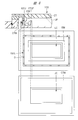
- FIG. 6 is a diagram schematically illustrating a correspondence relationship between a cross-sectional configuration and a planar configuration of a portion that supports the upper electrode UE in the plasma atomic layer growth apparatus 100.
- 6 corresponds to a cross-sectional view
- the center view of FIG. 6 corresponds to a plan view seen from below through the adhesion preventing member CTM
- the lower view of FIG. This corresponds to a plan view seen from below without omitting the member CTM.
- an insulating support member ISM is provided so as to surround and surround the rectangular upper electrode UE, and an inert gas supply unit IGSU is provided so as to surround the support member ISM.
- this inert gas supply part IGSU a plurality of supply ports FO for supplying an inert gas are formed.
- the adhesion prevention member CTM is provided so that the upper electrode UE may be separated and enclosed. Therefore, as can be seen by overlapping the center view of FIG. 6 and the lower view of FIG. 6, the adhesion preventing member CTM includes the insulating support member ISM and the inert gas supply part IGSU in plan view. Is arranged.
- the plasma atomic layer growth apparatus 100 in the present embodiment is configured as described above, and the features thereof will be described below.
- the first characteristic point in the present embodiment is that an adhesion preventing member CTM is provided so as to surround the upper electrode UE in a plan view. Thereby, it can prevent that a film
- the member provided around the upper electrode UE may be close to the discharge space, and film adhesion is likely to occur. Therefore, in the present embodiment, the adhesion preventing member CTM is provided so as to surround the upper electrode UE in plan view. Thereby, it can prevent effectively that a film
- the technical significance of providing the adhesion preventing member CTM so as to surround the upper electrode UE is as follows. For example, in the plan view, when the adhesion preventing member CTM is not provided so as to overlap with the member provided around the upper electrode UE, the film adheres to the member provided around the upper electrode UE. And when the thickness of the film
- the member provided around the upper electrode UE is provided close to the upper electrode UE disposed above the discharge space, and the foreign matter peeled off from the member provided around the upper electrode UE is easily attaches to the substrate 1S mounted on the lower electrode BE located below the discharge space.
- the film quality (quality) of the film formed on the substrate 1S is deteriorated by the foreign matter. That is, in order to improve the film quality of the film formed on the substrate 1S, it is important to suppress the foreign matter generated from the members provided around the upper electrode UE from adhering to the substrate 1S.
- the member provided around the upper electrode UE is provided in the vicinity of the upper electrode UE, which means that the upper electrode is disposed above the substrate 1S mounted on the lower electrode BE in a plan view. It means that members provided around the UE are arranged close to each other. As a result, the film quality of the film formed on the substrate 1S is greatly affected by the foreign matter generated by the peeling of the film attached to the member provided around the upper electrode UE. Therefore, in order to improve the film quality of the film formed on the substrate 1S, it is important to prevent the film from adhering to the members provided around the upper electrode UE. In order to realize this, In the present embodiment, the adhesion preventing member CTM is provided so as to surround the upper electrode UE in plan view. That is, the first feature point in the present embodiment has a technical significance of preventing the film from adhering to members provided around the upper electrode UE, and is thereby formed on the substrate 1S. Degradation of the film quality can be suppressed.
- the adhesion of the film to the member provided around the upper electrode UE is prevented, while the adhesion preventing member provided to surround the upper electrode UE.
- a film adheres to the CTM. Therefore, a part of the film adhering to the adhesion preventing member CTM may be peeled off to become a foreign substance.
- the adhesion preventing member CTM is configured to be removable. For this reason, for example, when the thickness of the film adhering to the adhesion preventing member CTM reaches a predetermined thickness, the film adhering to the adhesion preventing member CTM is removed by wet etching after removing the adhesion preventing member CTM. Then, the maintenance work for attaching the adhesion preventing member CTM from which the film has been removed is performed again, whereby generation of foreign matter from the adhesion preventing member CTM can be suppressed.
- the film adhered to the adhesion preventing member CTM is removed by wet etching or the like, and the film is formed again. It is conceivable to attach the removed adhesion-preventing member CTM. Also in this case, it is considered that the generation of foreign matters from members provided around the upper electrode UE can be suppressed.
- an insulating support member ISM that supports the upper electrode UE will be described as an example of a member provided around the upper electrode UE.
- the upper electrode UE is supported by an insulating support member ISM. From this, for example, in order to remove the film attached to the insulating support member ISM, the insulating support member ISM that fixes the upper electrode UE is removed, and the film attached to the insulating support member ISM is removed by wet etching. Conceivable.
- the attachment position of the upper electrode UE is different from the previous attachment position.
- the state of plasma discharge between the upper electrode UE and the lower electrode BE changes. That is, in the method of removing the insulating support member ISM and cleaning it by wet etching, the mounting position of the insulating support member ISM cannot be reproduced. As a result, the mounting position of the upper electrode UE supported by the insulating support member ISM changes, and plasma discharge This causes a side effect that the film forming conditions represented by this state change. In this case, the quality of the film formed on the substrate may vary.
- an insulating support member ISM that supports the upper electrode UE is provided around the upper electrode UE, and a film adheres to the insulating support member ISM.
- the deposition preventing member CTM is provided so as to surround the upper electrode UE.
- the adhesion preventing member CTM is disposed so as to overlap the insulating support member ISM in plan view.
- the present embodiment it is unnecessary to attach the insulating support member ISM again after removing the insulating support member ISM, performing wet etching, and the mounting position of the upper electrode UE is the previous mounting position. Therefore, the side effect of changing the film forming conditions due to the difference between the two can be prevented.
- the film adhering to the adhesion preventing member CTM is removed by wet etching or the like, and the adhesion removing member from which the film is removed again. Attaching the CTM is carried out.
- FIG. As shown in FIG.
- the attachment position of the upper electrode UE does not differ from the previous attachment position. That is, after removing the adhesion preventing member CTM, even if the film adhering to the adhesion preventing member CTM is removed and the adhesion preventing member CTM from which the film is removed is attached again, the attachment position of the upper electrode UE is not changed. There is no side effect of changing the film forming conditions due to the difference from the previous mounting position. From this, according to the first feature point in the present embodiment, it is possible to obtain a remarkable effect that the quality of the film formed on the substrate can be improved without changing the film forming conditions. .
- the second feature point in the present embodiment is that, for example, as shown in FIGS. 2 and 5, an adhesion preventing member CTM is provided so as to surround and surround the upper electrode UE.
- an adhesion preventing member CTM is provided so as to surround and surround the upper electrode UE.
- transformation and damage of the upper electrode UE and the deposition preventing member CTM can be prevented.
- the upper electrode UE is made of a conductor
- the deposition preventing member CTM is made of an insulator (ceramic). Therefore, the thermal expansion coefficient of the upper electrode UE and the thermal expansion coefficient of the deposition preventing member CTM are greatly different.
- the adhesion preventing member CTM when the adhesion preventing member CTM is formed so as to closely surround the upper electrode UE, the upper electrode UE and the anti-adhesion are caused by the difference between the thermal expansion coefficient of the upper electrode UE and the thermal expansion coefficient of the adhesion preventing member CTM. There is a possibility that each of the landing members CTM is deformed due to distortion. And when distortion becomes large, there exists a possibility that the adhesion prevention member CTM comprised from the ceramic may be damaged especially. For this reason, in the present embodiment, for example, as shown in FIG. 5, the adhesion preventing member CTM is provided so as to surround and surround the upper electrode UE. In other words, a gap is provided between the upper electrode UE and the deposition preventing member CTM.
- each volume expansion of the upper electrode UE and the adhesion prevention member CTM is absorbed by a clearance gap. Further, deformation and breakage of the upper electrode UE and the adhesion preventing member CTM can be suppressed.
- a gap is inevitably formed between the upper electrode UE and the deposition preventing member CTM as shown in FIG.
- a film is formed in the gap between the upper electrode UE and the adhesion-preventing member CTM due to the characteristics of the plasma atomic layer growth apparatus that a film is formed to every corner in the film formation container including a fine gap. It will be.
- a part of the insulating support member ISM is provided for the same reason that a gap is provided between the deposition preventing member CTM and the upper electrode UE in order to prevent deformation and breakage due to the difference in thermal expansion coefficient.
- a gap is also provided between the upper electrode UE and the upper electrode UE.
- the upper electrode UE is “separated” in consideration of the difference in the coefficient of thermal expansion between the members. If the second feature point that the adhesion preventing member CTM is provided so as to surround the upper electrode UE, for example, an unnecessary film may be attached to a part of the insulating support member ISM that supports the upper electrode UE.
- the configuration of the second feature point described above is However, it is not enough, and a device for further improvement is required. Therefore, in the present embodiment, while adopting the configuration of the second feature point described above, a device is devised to almost completely prevent the film from adhering to the insulating support member ISM that supports the upper electrode UE.
- This ingenuity is the third feature point in the present embodiment.
- the third feature point in the present embodiment will be described.
- the third characteristic point in the present embodiment is that an inert gas supply unit IGSU that supplies an inert gas to a gap between the upper electrode UE and the deposition preventing member CTM is provided.
- an inert gas supply unit IGSU formed by processing the top plate CT outside the top plate support portion CTSP that fixes the insulating support member ISM that supports the upper electrode UE is provided. Is provided.
- the inert gas supply part IGSU is connected with the inert gas supply path SRT1 which consists of the clearance gap between the adhesion prevention member CTM and the top-plate support part CTSP, and the clearance gap between the adhesion prevention member CTM and the insulation support member ISM.
- This inert gas supply path SRT1 functions as a path through which the inert gas supplied from the inert gas supply part IGSU flows in a direction approaching the upper electrode UE, and is between the deposition member CTM and the upper electrode UE.
- the gap and the gap between the insulating support member ISM and the upper electrode UE are connected.
- the inert gas supplied from the inert gas supply part IGSU passes along the inert gas supply path SRT1, and the adhesion prevention member CTM and the upper electrode UE And the gap between the insulating support member ISM and the upper electrode UE are filled.
- the second feature point in the present embodiment is adopted, gaps are formed between the deposition preventing member CTM and the upper electrode UE and between a part of the insulating support member ISM and the upper electrode UE. Even if this happens, these gaps are filled with an inert gas.
- the raw material is formed in a gap formed between the deposition preventing member CTM and the upper electrode UE and between a part of the insulating support member ISM and the upper electrode UE by the inert gas supplied from the inert gas supply unit IGSU. Intrusion of gas and reaction gas is prevented. As a result, even if a gap formed between a part of the insulating support member ISM and the upper electrode UE is provided, it is possible to prevent the source gas and the reaction gas from entering the gap. It is possible to prevent the film from adhering to a part of the member ISM.
- the anti-adhesion member CTM is provided so as to surround the upper electrode UE “separately” in consideration of the difference in the coefficient of thermal expansion between the members.
- the second feature point in the present embodiment for example, it is possible to prevent unnecessary films from adhering to a part of the insulating support member ISM that supports the upper electrode UE. That is, by adopting both the second feature point and the third feature point in the present embodiment, the film adheres to the insulating support member ISM that supports the upper electrode UE while lowering the deformation and breakage potential of the member. This can be almost completely prevented.
- the deposition preventing member CTM As a method of fixing the deposition preventing member CTM, the top plate support portion CTSP sandwiching the inert gas supply path SRT1 and the deposition preventing member CTM are secured by a securing member (screw), thereby the deposition preventing member CTM. Can be fixed to the top plate support part CTSP. However, since the inert gas supply path SRT1 sandwiched between the top plate support part CTSP and the deposition preventing member CTM is disposed at a position close to the discharge space, the inert gas supply from the inert gas supply part IGSU is not supplied.
- a securing member screw
- the raw material gas and the reactive gas (active species) are likely to enter the inert gas supply path SRT1.
- screw holes are provided in both the top plate support portion CTSP and the adhesion preventing member CTM, and are fixed with screws (fixing members).
- the screws are firmly fixed by the film attached to the screw holes. For this reason, when a film adheres to the screw hole, a large force is required to remove the screw, which may damage the screw itself or the adhesion preventing member CTM.
- the film is difficult to adhere to the fine gaps of the screw holes, and the screws can be suppressed from being firmly fixed, As a result, it is possible to prevent damage to the screw itself or the adhesion preventing member CTM.
- a contrivance is provided to provide a fixing portion for fixing the deposition preventing member CTM as far as possible from the discharge space, and this contrivance point is the fourth feature point in the present embodiment.
- the fourth feature point in the present embodiment is that, for example, as shown in FIG. 5, the upper electrode is formed by configuring the shape of the adhesion-preventing member CTM from an L shape having a horizontal portion HZPT and a vertical portion VTPT. It is assumed that an inert gas supply path SRT2 through which an inert gas flows in a direction away from the UE is provided.
- the fourth feature of the present embodiment is that the vertical channel is formed in the inert gas supply channel SRT2 by the above-described premise configuration, and the adhesion member CTM and the non-adhesive member C
- the connection point CU for connecting the active gas supply unit IGSU is provided.
- the fourth feature point in the present embodiment is that, for example, screw holes are provided in both the vertical portion VTPT of the deposition preventing member CTM and the vertical portion VTPT2 of the inert gas supply unit IGSU and fixed with screws.
- the connection portion CU is formed.
- the fixing portion (connecting portion) for fixing the deposition-preventing plate CTM is formed as far as possible from the discharge space.
- the raw material gas and the reactive gas (active species) are present up to the fixing part (connecting part) of the deposition preventing CTM. This makes it difficult to reach the film, and this makes it difficult for the film to adhere to the fine gaps in the screw holes. Therefore, according to the fourth feature point in the present embodiment, it is possible to prevent the screw itself or the adhesion-preventing member CTM from being damaged by preventing the screw from being firmly fixed.
- not only the fixing hole (screw hole) SH but also a convex portion SU may be provided in the vertical portion of the deposition preventing member CTM.
- the connection between the vertical portion of the deposition preventing member CTM and the vertical portion of the inert gas supply unit is performed by both the fixing means by inserting the screw into the fixing hole SH and the fixing means by the convex portion SU.
- the connection reliability between the deposition preventing member CTM and the inert gas supply unit IGSU can be improved.
- the fifth feature point in the present embodiment is that, for example, as shown in FIG. 5, the inert gas is supplied separately from the gas supply unit GSU that supplies the source gas and the reaction gas into the film forming container.
- the inert gas supply unit IGSU is provided. Accordingly, the inert gas supply unit IGSU is provided so that the inert gas can be efficiently supplied to a place where it is desired to prevent the unnecessary film from being attached, in particular, without being influenced by the arrangement position of the gas supply unit GSU.
- the position can be designed.
- the inert gas can be supplied through a different path from the gas supply unit GSU for supplying the source gas and the reactive gas, the flow of the raw material gas and the reactive gas supplied to the discharge space SP is ineffective. It is possible to suppress the adverse effect of the flow of the active gas. As a result, according to the fifth feature point in the present embodiment, it is possible to suppress a decrease in uniformity of the source gas and the reaction gas on the substrate 1S caused by supplying the inert gas into the film formation container. Accordingly, it is possible to prevent the uniformity of the film formed on the substrate 1S from being lowered while supplying the inert gas.
- the distance “a” between the outer peripheral end surface of the substrate 1S and the outer peripheral end surface of the upper electrode is preferably 0.1 mm or more.
- the plasma atomic layer growth apparatus 100 according to the present embodiment. Then, it is 50 mm. If the distance “a” becomes too small, the flow of the source gas and the reaction gas supplied onto the substrate 1S is easily affected by the flow of the inert gas, and the source gas and the reaction gas are uniformly distributed on the substrate 1S. There is a concern about the decline of sex. On the other hand, if the distance “a” becomes too large, the apparatus size of the plasma atomic layer growth apparatus 100 becomes large, so that a desirable allowable range exists.
- the distance “b” indicating the diameter of the inert gas supply path SRT1 and the distance “c” indicating the diameter of the inert gas supply path SRT2 can be, for example, 20 mm or less.
- the distance “b” and the distance “c” may be set to almost zero. This is because, in this case, even if the distance “b” and the distance “c” are almost zero, the inner surface of the adhesion-preventing member CTM has a rough surface, so that a path through which the inert gas flows is secured. It is.
- the distance “d” between the deposition preventing member formed on the lower surface of the upper electrode UE and the deposition preventing member CTM is desirably in the range of 0.1 mm to 20 mm.
- the thickness is set to 2 mm.
- the small distance “d” prevents the raw material gas and the reactive gas from entering the inert gas supply path SRT1 to prevent the film from adhering to the insulating support member ISM and the top plate support part CTSP. it can.
- the distance “e”, which is the thickness of the deposition preventing member CTM and the thickness of the deposition preventing member formed on the lower surface of the upper electrode UE, is desirably 2 mm or more and 100 mm or less. In the plasma atomic layer growth apparatus 100 in the form, the thickness is 10 mm.
- the weight of the deposition preventing member CTM and the weight of the deposition preventing member formed on the lower surface of the upper electrode UE are increased, and thus the maintenance workability is lowered. Therefore, a desirable tolerance exists.
- the distance “f” between the deposition preventing member CTM and the gas supply unit GSU is preferably in the range of 0.1 mm to 50 mm.
- the distance “f” is 10 mm. Yes. Since the distance “f” is small, it is possible to prevent the source gas and the reaction gas from entering the inside of the inert gas supply path SRT2. However, when the distance “f” is too small, the deposition container and the deposition preventing member CTM come into contact with each other and the deposition preventing member CTM is damaged when the top plate CT and the deposition container are attached and detached during the maintenance work. There is a desirable tolerance.
- the distance “g” indicating the length of the vertical portion VTPT of the deposition preventing member CTM is preferably in the range of 2 mm to 200 mm, and is, for example, 50 mm in the plasma atomic layer growth apparatus 100 in the present embodiment. Since the distance “g” is large, the source gas and the reaction gas can be prevented from entering the inert gas supply path SRT2.
- the distance “h” from the bottom surface of the deposition preventing member CTM to the attachment position of the connecting portion CU is desirably in the range of 2 mm to 200 mm.
- it is set to 40 mm. .
- the distance “h” is large, it is possible to prevent the film from adhering to the connection portion due to the source gas and the reaction gas entering the inside of the inert gas supply path SRT2.
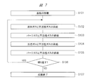
- FIG. 7 is a flowchart for explaining the atomic layer growth method in the present embodiment
- FIGS. 8A to 8E are diagrams schematically showing a process of forming a film on a substrate.
- the substrate 1S is mounted on the lower electrode BE (stage) of the plasma atomic layer growth apparatus 100 shown in FIG. 5 (S101 in FIG. 7).
- the source gas is supplied from the gas supply unit GSU of the plasma atomic layer growth apparatus 100 shown in FIG. 5 to the inside of the film formation container, and the inert gas is supplied from the inert gas supply unit IGSU to the inert gas supply path SRT1 and It supplies to the inert gas supply path SRT2 (S102 of FIG. 7).
- the source gas is supplied into the film formation container for 0.1 seconds, for example.
- the inert gas IG and the source gas SG are supplied into the film forming container, and the source gas SG is adsorbed on the substrate 1S to form the adsorption layer ABL.
- the purge gas is supplied from the gas supply unit GSU, and the inert gas is supplied from the inert gas supply unit IGSU to the inert gas supply path SRT1 and the inert gas supply path SRT2. (S103 in FIG. 7).
- the purge gas is supplied into the film forming container, while the source gas is discharged from the exhaust unit to the outside of the film forming container.
- the purge gas is supplied into the film formation container for 0.1 seconds, for example.
- the exhaust unit exhausts the source gas and the purge gas in the film formation container for 2 seconds, for example.
- the inert gas IG and the purge gas PG1 are supplied into the film formation container, and the source gas SG not adsorbed on the substrate 1S is purged from the film formation container.
- the reactive gas is supplied from the gas supply unit GSU, and the inert gas is supplied from the inert gas supply unit IGSU to the inert gas supply path SRT1 and the inert gas supply path SRT2 (S104 in FIG. 7).
- the reactive gas is supplied into the film forming container.
- the reaction gas is supplied into the film formation container for 1 second, for example.
- plasma discharge is generated by applying a discharge voltage between the upper electrode UE and the lower electrode BE shown in FIG. As a result, radicals (active species) are generated in the reaction gas. In this way, as shown in FIG.
- the inert gas IG and the reaction RAG are supplied into the film formation container, and the adsorption layer adsorbed on the substrate 1S is chemically reacted with the reaction gas RAG. By reacting, a thin film layer composed of the atomic layer ATL is formed.
- the purge gas is supplied from the gas supply unit GSU, and the inert gas is supplied from the inert gas supply unit IGSU to the inert gas supply path SRT1 and the inert gas supply path SRT2. (S105 in FIG. 7).
- the purge gas is supplied into the film forming container, while the reaction gas is discharged from the exhaust unit to the outside of the film forming container.
- the reaction gas is supplied into the film formation container for 0.1 seconds, for example.
- the exhaust unit exhausts the source gas and the purge gas in the film formation container for 2 seconds, for example.
- the inert gas IG and the purge gas PG2 are supplied into the film formation container, and excess reaction gas RAG that is not used for the reaction is purged from the film formation container.
- a thin film layer composed of one atomic layer ATL is formed on the substrate 1S. Thereafter, the above-described steps (S102 in FIG. 7 to S105 in FIG. 7) are repeated a predetermined number of times (S106 in FIG. 7), thereby forming a thin film layer composed of a plurality of atomic layers ATL. Thus, the film forming process is completed (S107 in FIG. 7).
- the atomic layer growth method according to the present embodiment includes (a) a step of supplying a source gas into a film formation container in which a substrate is disposed, and (b) after the step (a), A step of supplying a first purge gas, a step of supplying a reactive gas into the film formation container after the steps (c) and (b), and a second purge gas in the film formation vessel after the steps (d) and (c).
- a step of supplying is that the inert gas is further supplied into the film formation container over the steps (a), (b), (c), and (d). In the point.
- the source gas, the purge gas, and the reactive gas are supplied from the gas supply unit GSU, while the inert gas is , Supplied from an inert gas supply unit IGSU different from the gas supply unit GSU.
- the inert gas can be efficiently used at a place where it is desired to prevent adhesion of an unnecessary film (a place that greatly affects the film quality of the film formed on the substrate 1S) without being influenced by the arrangement position of the gas supply unit GSU. Can be supplied. From this, according to this Embodiment, the film quality of the film
- the pressure fluctuation in the film formation container in steps (a), (b), (c), and (d) supplies the inert gas. It can be made smaller than the pressure fluctuation in the film formation container when not. This is because the difference between the flow rate of the source gas, the flow rate of the purge gas, and the flow rate of the reactive gas is not supplied to the film formation container throughout the steps (a), (b), (c), and (d). This is because it is relaxed by the flow rate of the active gas.
- the combined flow rate of the raw material gas and the inert gas, the combined flow rate of the purge gas and the inert gas, and the combined flow rate of the reactive gas and the inert gas are substantially equal.
- the flow rate of the inert gas supplied into the film formation container is adjusted over the steps (a), (b), (c), and (d).
- the pressure fluctuation in the film formation container over the steps (a), (b), (c), and (d) causes the inert gas to flow. This is smaller than the pressure fluctuation in the film formation container when not supplied.
- an aluminum oxide film is formed by using TMA as a raw material, using oxygen gas as a reaction gas, and using nitrogen gas as a purge gas. Can do.
- the aluminum oxide film formed on the substrate can be formed as a film constituting a part of the protective film that protects the light emitting layer of the organic EL element.
- the film formed on the substrate can be not only an aluminum oxide film but also various kinds of films represented by a silicon oxide film.
- the film formed over the substrate by the atomic layer growth method in this embodiment can be formed as a film that forms a gate insulating film of a field-effect transistor (semiconductor element).
- the present invention is not limited to this, and the present invention can also be applied to a configuration in which an adhesion preventing member is provided so as to support the substrate on the upper electrode and surround the lower electrode facing the upper electrode.
- 100 plasma atomic layer growth apparatus BE lower electrode CTM adhesion preventing member CU connecting part FU fixing part GSU gas supply part HZPT horizontal part IGSU inert gas supply part ISM insulating support member PCE1 part PCE2 part PCE3 part PCE4 part PT1 part PT3 part PT PT4 site SRT1 inert gas supply channel SRT2 inert gas supply channel SS1 side surface SS2 side surface SS3 side surface SS4 side surface SUR surface UE upper electrode VTPT vertical region VTPT2 vertical region
Landscapes
- Chemical & Material Sciences (AREA)
- Engineering & Computer Science (AREA)
- Physics & Mathematics (AREA)
- Plasma & Fusion (AREA)
- Organic Chemistry (AREA)
- General Chemical & Material Sciences (AREA)
- Chemical Kinetics & Catalysis (AREA)
- Materials Engineering (AREA)
- Mechanical Engineering (AREA)
- Metallurgy (AREA)
- Analytical Chemistry (AREA)
- Electromagnetism (AREA)
- Optics & Photonics (AREA)
- Chemical Vapour Deposition (AREA)
- Plasma Technology (AREA)
- Electroluminescent Light Sources (AREA)
- Formation Of Insulating Films (AREA)
Abstract
基板上に形成される膜の膜質を向上することができるプラズマ原子層成長装置を提供する。原子層成長装置は、基板1Sを保持する下部電極BEと、下部電極BEと対向配置された上部電極UEとの間にプラズマ放電を生じさせることにより、基板1S上に原子層単位で膜を成膜するプラズマ原子層成長装置であって、平面視において、上部電極UEを離間して囲む絶縁体からなる防着部材CTMを備える。
Description
本発明は、原子層成長技術に関する。
特開2006-351655号公報(特許文献1)には、CVD法(Chemical Vapor Deposition)やスパッタリング法を使用した成膜装置において、防着板を使用するとともに、チャンバの内壁に堆積した堆積物を非晶質膜で覆う技術が記載されている。
特開2009-62579号公報(特許文献2)には、成膜室内の複数の側面部に対応させて複数の防着板を配置し、かつ、防着板を複数に分割して、近接する防着板同士の間に隙間を設ける技術が記載されている。
特開2012-52221号公報(特許文献3)には、スパッタリング空間の圧力値に基づいて、スパッタリング空間内に導入されるガス流量と、真空チャンバの内壁と防着板との間の空間に導入されるガス流量との流量比を制御する技術が記載されている。
特開2014-133927号公報(特許文献4)には、複数の貫通孔が形成された一対の防着板を処理室の内壁に近接して配置する技術が記載されている。
特開2001-316797号公報(特許文献5)には、基板キャリアの表面への膜の付着を防止する防着部材を、基板キャリアの底面に取り付ける技術が記載されている。
原子層成長法は、原料ガスと反応ガスとを基板上に交互に供給することにより、基板上に原子層単位で膜を形成する成膜方法である。この原子層成長法は、原子層単位で膜を形成することから、段差被覆性や膜厚制御性に優れているという利点を有している。一方、原子層成長法を具現化する原子層成長装置では、段差被覆性に優れている利点の裏返しとして、成膜条件の変化を伴うことなく除去することが困難な場所にも容易に膜が形成されやすい。このことから、原子層成長装置では、成膜条件の変化を伴うことなく除去することが困難な場所に形成された膜の剥離に起因する異物の発生によって、基板上に形成される膜の膜質が劣化することが懸念される。
その他の課題と新規な特徴は、本明細書の記述および添付図面から明らかになるであろう。
一実施の形態における原子層成長装置は、基板を保持する第1電極と、第1電極と対向配置された第2電極との間にプラズマ放電を生じさせることにより、基板上に原子層単位で膜を成膜する原子層成長装置であって、平面視において、第2電極を離間して囲む絶縁体からなる防着部材を備える。
一実施の形態における原子層成長装置によれば、基板上に形成される膜の膜質を向上することができる。
<原子層成長装置に特有の改善の余地>
例えば、プラズマCVD装置では、基板を保持する下部電極と、下部電極と対向配置される上部電極との間に複数の原料ガスを供給しながら、下部電極と上部電極との間にプラズマ放電を生じさせる。これにより、プラズマCVD装置では、プラズマ放電で生じた活性種(ラジカル)による化学反応により、基板上に膜を形成する。このとき、プラズマCVD装置では、主にプラズマ放電が形成されている領域(放電空間)に膜が形成される。これは、プラズマCVD装置で使用される原料ガスとして、放電空間に局在化させるために拡散しにくい性質を有している原料ガスが使用されるとともに、複数の原料ガスからプラズマ放電によって活性種(ラジカル)が生じて初めて膜材料が形成されるからである。したがって、プラズマCVD装置では、放電空間から離れた場所(プラズマ放電が生じない場所)には膜が形成されにくい傾向を示すことになる。
例えば、プラズマCVD装置では、基板を保持する下部電極と、下部電極と対向配置される上部電極との間に複数の原料ガスを供給しながら、下部電極と上部電極との間にプラズマ放電を生じさせる。これにより、プラズマCVD装置では、プラズマ放電で生じた活性種(ラジカル)による化学反応により、基板上に膜を形成する。このとき、プラズマCVD装置では、主にプラズマ放電が形成されている領域(放電空間)に膜が形成される。これは、プラズマCVD装置で使用される原料ガスとして、放電空間に局在化させるために拡散しにくい性質を有している原料ガスが使用されるとともに、複数の原料ガスからプラズマ放電によって活性種(ラジカル)が生じて初めて膜材料が形成されるからである。したがって、プラズマCVD装置では、放電空間から離れた場所(プラズマ放電が生じない場所)には膜が形成されにくい傾向を示すことになる。
これに対し、例えば、プラズマ原子層成長装置では、基板を保持する下部電極と、下部電極と対向配置される上部電極との間に、原料ガスと反応ガスとを交互に供給し、かつ、反応ガスを供給する際にプラズマ放電することにより、基板上に原子層単位で膜を形成する。このとき、プラズマ原子層成長装置では、原子層単位で膜を形成することにより、段差被覆性に優れた膜を形成することができる。特に、プラズマ原子層成長装置では、段差被覆性を良好にするため、原料ガスとして拡散しやすい材料が使用されるとともに、それぞれのガス(原料ガスやパージガスや反応ガス)が成膜容器内に充分に拡散するだけの時間を確保しながら、それぞれのガスを交互に供給している。このため、例えば、原料ガスや反応ガスは、基板上だけでなく、成膜容器の隅々まで行き渡ることになる。さらには、プラズマ原子層成長装置においては、反応ガスをプラズマ放電させることにより活性種(ラジカル)を形成して、この活性種と基板に吸着した原料ガスとが反応して膜が形成されるだけでなく、プラズマ放電によって活性種(ラジカル)が生じない状態においても、原料ガスと反応ガスとが反応しやすい傾向がある。したがって、プラズマ原子層成長装置では、プラズマ放電が生じていない成膜容器の微細な隙間においても、原料ガスと反応ガスが反応して膜が形成されることになる。つまり、原子層成長装置では、(1)原子層単位で膜を形成すること、(2)成膜容器の隅々まで原料ガスや反応ガスが行き渡ること、(3)プラズマ放電が生じていない場所でも原料ガスと反応ガスとが反応しやすいことという特徴を有する結果、微細な隙間にも膜が形成されることになる。
このようにプラズマ原子層成長装置においては、基板上だけでなく、微細な隙間を含む成膜容器内の隅々まで膜が形成されてしまうという性質があることになる。そして、この性質に起因して、プラズマ原子層成長装置に特有の改善の余地が存在することを本発明者は見出したので、以下に、この改善の余地について説明することにする。
例えば、プラズマ原子層成長装置において、上部電極は、例えば、絶縁支持部材で支持される。ここで、上述したように、プラズマ原子層成長装置では、成膜容器の隅々まで膜が形成されてしまうことから、絶縁支持部材にも膜が形成されることになる。そして、絶縁支持部材に付着した膜の膜厚が厚くなると、付着した膜の一部が絶縁支持部材から剥離して異物となる。この異物は、基板上に形成される膜の膜質を劣化させる要因となる。このことから、基板上に形成される膜の膜質(品質)を向上するためには、絶縁支持部材に付着した膜を除去する必要がある。
この点に関し、例えば、成膜容器内に、例えば、NF3ガスなどから構成されるクリーニングガスを導入してドライエッチングを実施することにより、絶縁支持部材に付着した膜を除去することが考えられる。ところが、プラズマ原子層成長装置では、微細な隙間を含む成膜容器の隅々まで膜が形成される一方、クリーニングガスによるドライエッチングでは、プラズマ放電が生じている場所しか膜の除去が行なわれないとともに、クリーニングガスが微細な隙間を含む成膜容器の隅々まで行き渡ることは困難である。さらには、例えば、プラズマ原子層成長装置で形成する膜として、酸化アルミニウム膜(Al2O3膜)を一例として挙げることができるが、この酸化アルミニウム膜は、ドライエッチングで除去することが困難である。したがって、プラズマ原子層成長装置においては、クリーニングガスを使用したドライエッチングでは、成膜容器の隅々まで形成された膜を除去することは困難であることから、例えば、絶縁支持部材に付着した膜の除去にもドライエッチングを使用することは困難となる。
そこで、例えば、上部電極を固定する絶縁支持部材を取り外して、絶縁支持部材に付着した膜をウェットエッチングにより除去することが考えられる。ところが、絶縁支持部材を取り外して、ウェットエッチングを施した後、再び、絶縁支持部材を取り付けると、上部電極の取り付け位置が以前の取り付け位置と異なることになる。この場合、上部電極と下部電極との間のプラズマ放電の状態が変化する。つまり、絶縁支持部材を取り外して、ウェットエッチングでクリーニングする方法では、絶縁支持部材の取り付け位置を再現できなくなる結果、絶縁支持部材で支持される上部電極の取り付け位置が変わり、プラズマ放電の状態に代表される成膜条件が変化してしまう。この場合、基板上に形成される膜の品質が変動するおそれがある。さらには、絶縁支持部材に付着した膜をウェットエッチングにより除去する方法では、成膜容器内を大気圧に開放した後、絶縁支持部材を取り出す必要があり、メンテナンス作業性が低下することになる。
以上のことから、プラズマ原子層成長装置では、特に、基板上に形成される膜の膜質を向上し、かつ、成膜条件を変えることなく、上部電極を支持する絶縁支持部材に付着した膜を除去することが困難であることがわかる。そこで、本実施の形態では、上部電極を支持する絶縁支持部材に付着した膜を除去する工夫を施している。以下では、この工夫を施した本実施の形態における技術的思想について説明することにする。
<プラズマ原子層成長装置の全体構成>
図1は、本実施の形態におけるプラズマ原子層成長装置100の全体構成を模式的に示す断面図である。本実施の形態におけるプラズマ原子層成長装置100は、原料ガスと反応ガスとを交互に供給することにより、基板1S上に原子層単位で膜を形成するように構成されている。その際、反応活性を高めるため、基板1Sを加熱することができる。
図1は、本実施の形態におけるプラズマ原子層成長装置100の全体構成を模式的に示す断面図である。本実施の形態におけるプラズマ原子層成長装置100は、原料ガスと反応ガスとを交互に供給することにより、基板1S上に原子層単位で膜を形成するように構成されている。その際、反応活性を高めるため、基板1Sを加熱することができる。
本実施の形態では、原料として、TMA(Tri-Methyl-Aluminum)を使用し、反応活性を高めるため、プラズマ放電が行なわれる。本実施の形態では、プラズマ放電を行なうため、平行平板電極が使用される。
図1に示すように、本実施の形態におけるプラズマ原子層成長装置100は、成膜容器CBを有している。この成膜容器CBには、基板1Sを保持するステージが配置されており、このステージは、下部電極BEとして機能する。また、ステージは、ヒータを備え、基板1Sの温度を調整することができるように構成されている。例えば、本実施の形態におけるプラズマ原子層成長装置100の場合、ステージ上に保持される基板1Sは、50℃~200℃に加熱される。そして、成膜容器CBは、真空に維持される。
次に、図1に示すように、成膜容器CBには、原料ガスやパージガスや反応ガスを供給するガス供給部GSUが設けられているとともに、原料ガスやパージガスや反応ガスを排気するガス排気部GVUが設けられている。例えば、ガス供給部GSUとガス排気部GVUとは、互いに対向する位置に設けられており、ガス供給部GSUから供給されたガスは、成膜容器CB内の放電空間SPを通って、ガス排気部GVUから排気される。
さらに、成膜容器CB内には、下部電極BE上に搭載されている基板1Sの上方に位置する放電空間を挟んで、上部電極UEが配置されている。すなわち、上部電極UEは、基板1Sが搭載された下部電極BEと対向するように配置されている。そして、上部電極UEの上方に天板CTが配置されており、この天板CTには、上部電極UEを支持するための天板支持部CTSPが設けられている。さらに、天板支持部CTSPと密着するように絶縁支持部材ISMが配置されており、この絶縁支持部材ISMによって、上部電極UEが支持されている。そして、図1に示すように、本実施の形態におけるプラズマ原子層成長装置100は、平面視において、上部電極UEを離間して囲む絶縁体からなる防着部材CTMを有しており、平面視において、防着部材CTMは、絶縁支持部材ISMと重なるように配置されている。
続いて、図1に示すように、天板CTには、成膜容器CB内に窒素ガスなどの不活性ガスを供給する不活性ガス供給部IGSUが設けられている。このように、本実施の形態におけるプラズマ原子層成長装置100には、原料ガスやパージガスや反応ガスを供給するガス供給部GSUの他に、不活性ガスを供給する不活性ガス供給部IGSUが別個に設けられている。
<防着部材の構成>
次に、本実施の形態における防着部材CTMの構成について説明する。図2は、上部電極UEを離間して囲むように設けられた本実施の形態における防着部材CTMの構成を模式的に示す図である。図2において、二点鎖線で示す直方体が上部電極UEの模式的な構成を示している。図2に示す上部電極UEは、図1に示す下部電極BEと対向する表面SURと、表面SURと交差する側面SS1と、側面SS1の反対側に位置する側面SS2と、表面SURおよび側面SS1と交差する側面SS3と、側面SS3の反対側に位置する側面SS4とを有する。そして、図2に示すように、本実施の形態における防着部材CTMは、上部電極UEを離間して取り囲むように構成されている。具体的に、本実施の形態における防着部材CTMは、上部電極UEの側面SS1と対向する部位(part)PT1と、上部電極UEの側面SS2と対向する部位PT2と、上部電極UEの側面SS3と対向する部位PT3と、上部電極UEの側面SS4と対向する部位PT4とを有する。一方、本実施の形態における防着部材CTMは、図2に示すように、上部電極UEの表面SURを露出するように、防着部材CTMの底部に開口部が形成されている。この結果、図2に示すように、本実施の形態における防着部材CTMの部位PT1~PT4のそれぞれは、水平部位と垂直部位とを有するL字形状をしていることになる。
次に、本実施の形態における防着部材CTMの構成について説明する。図2は、上部電極UEを離間して囲むように設けられた本実施の形態における防着部材CTMの構成を模式的に示す図である。図2において、二点鎖線で示す直方体が上部電極UEの模式的な構成を示している。図2に示す上部電極UEは、図1に示す下部電極BEと対向する表面SURと、表面SURと交差する側面SS1と、側面SS1の反対側に位置する側面SS2と、表面SURおよび側面SS1と交差する側面SS3と、側面SS3の反対側に位置する側面SS4とを有する。そして、図2に示すように、本実施の形態における防着部材CTMは、上部電極UEを離間して取り囲むように構成されている。具体的に、本実施の形態における防着部材CTMは、上部電極UEの側面SS1と対向する部位(part)PT1と、上部電極UEの側面SS2と対向する部位PT2と、上部電極UEの側面SS3と対向する部位PT3と、上部電極UEの側面SS4と対向する部位PT4とを有する。一方、本実施の形態における防着部材CTMは、図2に示すように、上部電極UEの表面SURを露出するように、防着部材CTMの底部に開口部が形成されている。この結果、図2に示すように、本実施の形態における防着部材CTMの部位PT1~PT4のそれぞれは、水平部位と垂直部位とを有するL字形状をしていることになる。
ここで、防着部材CTMの部位PT1~PT4のそれぞれには、固定部材を埋め込む複数の固定穴SHと、固定部材を支持する複数の凸部SUとが形成されている。これにより、防着部材CTMは、図2では図示されない固定部材で支持されることになる。このようにして、本実施の形態におけるプラズマ原子層成長装置には、上部電極UEを囲む防着部材CTMが設けられていることになる。
<防着部材の第1構成態様(一体化)>
図3は、本実施の形態における防着部材CTMの構成態様例を示す模式図である。図3に示す防着部材CTMの構成態様では、防着部材CTMを構成する部位PT1~PT4が一体的に形成されている。すなわち、図3に示す防着部材CTMの部位PT1~PT4は、継ぎ目のない一体物として形成されている。これにより、一体化された部位PT1~PT4から構成される防着部材CTMによれば、以下に示す利点を得ることができる。
図3は、本実施の形態における防着部材CTMの構成態様例を示す模式図である。図3に示す防着部材CTMの構成態様では、防着部材CTMを構成する部位PT1~PT4が一体的に形成されている。すなわち、図3に示す防着部材CTMの部位PT1~PT4は、継ぎ目のない一体物として形成されている。これにより、一体化された部位PT1~PT4から構成される防着部材CTMによれば、以下に示す利点を得ることができる。
すなわち、<原子層成長装置に特有の改善の余地>の欄で説明したように、プラズマ原子層成長装置では、放電空間から離れたプラズマ放電が生成されない場所においても膜が形成され、かつ、原子層単位で成膜されることに起因して、微細な隙間まで膜が形成されてしまう性質がある。このことから、プラズマ原子層成長装置では、例えば、上部電極を覆う防着部材CTMにも膜が付着する。この点に関し、図3に示す防着部材CTMの部位PT1~PT4は、継ぎ目のない一体物として形成されている。したがって、図3に示す防着部材CTMには、防着部材CTMに微細な隙間が形成されないことから、微細な隙間に膜が形成されて剥離することによる異物の発生を抑制することができる。つまり、成膜空間の隅々まで異物の発生源となる膜が形成されるプラズマ原子層成長装置では、異物の発生を極力低減できる部材を使用することが望まれている。この観点から、継ぎ目のない一体物として形成されている防着部材CTMは、異物の発生源を極力省いた望ましい部材ということができる。なぜなら、図3に示すように、防着部材CTMを継ぎ目のない一体物から構成する場合、そもそも、膜の除去が困難な微細な隙間が存在しないことから、微細な隙間に形成された膜の剥離に起因する異物の発生ポテンシャルを無くすことができるからである。つまり、継ぎ目のない一体物からなる防着部材CTMによれば、取り外して付着した膜を除去することにより、異物の発生ポテンシャルの低い防着部材CTMを提供することができる。この結果、図3に示す継ぎ目のない一体物からなる防着部材CTMによれば、基板上に異物が付着することを防止できることから、基板上に形成される膜の膜質(品質)を向上することができる。
さらに、プラズマ原子層成長装置では、平坦面と比べて微細な隙間に膜が形成されやすい性質がある。このため、継ぎ目のない一体物からなる防着部材CTMによれば、膜が形成されやすい微細な隙間が存在しないため、防着部材CTMのメンテナンス周期を長くすることができる利点を得ることができる。
<防着部材の第2構成態様(分割)>
図4は、本実施の形態における防着部材CTMの他の構成態様例を示す模式図である。図4に示す防着部材CTMの構成態様では、防着部材CTMを構成する部位PT1~PT4は、別々の部品(piece)から構成されている。すなわち、図4に示す防着部材CTMは、部位PT1に対応する部品PCE1と、部位PT2に対応する部品PCE2と、部位PT3に対応する部品PCE3と、部位PT4に対応する部品PCE4とから構成されている。このように、本実施の形態における防着部材CTMは、図3に示す継ぎ目のない一体物として構成するだけでなく、図4に示す別部品の組み合わせからも構成できる。
図4は、本実施の形態における防着部材CTMの他の構成態様例を示す模式図である。図4に示す防着部材CTMの構成態様では、防着部材CTMを構成する部位PT1~PT4は、別々の部品(piece)から構成されている。すなわち、図4に示す防着部材CTMは、部位PT1に対応する部品PCE1と、部位PT2に対応する部品PCE2と、部位PT3に対応する部品PCE3と、部位PT4に対応する部品PCE4とから構成されている。このように、本実施の形態における防着部材CTMは、図3に示す継ぎ目のない一体物として構成するだけでなく、図4に示す別部品の組み合わせからも構成できる。
ここで、図4に示す防着部材CTMは、別部品の組み合わせからも構成されているため、部品間に継ぎ目が存在することになる。このことから、図4に示す防着部材CTMでは、部品間に微細な隙間が存在することになり、この微細な隙間にも膜が形成されることになる。この結果、図4に示す防着部材CTMでは、微細な隙間に形成された膜の剥離に起因する異物の発生ポテンシャルが大きくなると考えられる。
この点に関し、図4に示す防着部材CTMでは、微細な隙間が形成されるが、図4に示す防着部材CTMを別部品の組み合わせから構成するという点によって、微細な隙間に形成された膜の剥離に起因する異物の発生ポテンシャルは低減することができるのである。
以下に、この点について説明する。別部品の組み合わせから防着部材CTMを形成する場合、確かに、部品間の継ぎ目に微細な隙間が形成されることから、微細な隙間に形成された膜の剥離に起因する異物の発生ポテンシャルが大きくなると考えられる。ただし、実際には、別部品の組み合わせから防着部材CTMを構成する場合、防着部材CTMは、それぞれの部品に分解して取り外すことができる。このように個々の部品に分解してしまえば、部品同士を組み合わせた場合に生じる微細な隙間は存在しなくなり、個々の部品をウェットエッチングすることで、微細な隙間に対応した部分に付着した膜を除去することができる。つまり、防着部材CTMが別部品の組み合わせから構成されている場合、組み合わせた段階では微細な隙間が存在するが、防着部材CTMを分解して取り外すことができる。このため、分解した部品ごとにウェットエッチングを施すことによって、微細な隙間に対応する個々の部品の部位に付着した膜でも充分に除去することができる。
上述したように、防着部材CTMを別部品の組み合わせから構成する場合、取り外した後に分解してウェットエッチングを施すことにより、異物の発生ポテンシャルの低い防着部材CTMを実現することができる。ただし、この場合、分解した部品を再度組み合わせると、分解前の防着部材CTMの取り付け形状や取り付け位置と、分解後の防着部材CTMの取り付け形状や取り付け位置とが微妙に異なることが考えられる。しかし、防着部材CTM自体は、上部電極や下部電極のように、プラズマ放電に直接関連性を有する部位ではないことから、防着部材CTMの取り付け形状や取り付け位置が分解前と分解後で微妙に相違しても、プラズマ放電特性に代表される成膜条件に及ぼす影響は大きくないと考えられる。このことから、防着部材CTMを別部品の組み合わせから構成する場合であっても、取り付け形状や取り付け位置が微妙に異なることに起因する成膜条件の変化はほとんどないものと考えることができる。たとえ、部品の取り付け形状や取り付け位置が微妙に異なることに起因する成膜条件の変化が生じるにしても、それは無視できるレベルと考えることができる。したがって、図4に示すように、防着部材CTMを別部品の組み合わせから構成する場合であっても、成膜条件を大幅に変化させることなく、部品に付着した膜の除去が可能であり、かつ、異物の発生ポテンシャルをある程度低くできる点で有用である。すなわち、防着部材CTMからの異物の発生を抑制する観点からは、図3に示す継ぎ目のない一体物からなる防着部材CTMが望ましい一方、図4に示す別部品の組み合わせからなる防着部材CTMによっても、基板上に異物が付着することを防止できることから、基板上に形成される膜の膜質(品質)を向上することができる。
ただし、上述したように、プラズマ原子層成長装置では、平坦面と比べて微細な隙間に膜が形成されやすい性質がある。このことから、防着部材CTMを別部品の組み合わせから構成すると、防着部材CTMを継ぎ目のない一体物から構成する場合に比べて、膜が形成されやすい微細な隙間が存在する分だけ、異物の発生ポテンシャルが高くなる。この結果、防着部材CTMのメンテナンス周期が短くなる。つまり、メンテナンス周期を長くする観点からは、防着部材CTMを別部品の組み合わせから構成する場合よりも、防着部材CTMを継ぎ目のない一体物から構成する場合のほうが望ましいといえる。
一方、図4に示すように、防着部材CTMを別部品の組み合わせから構成する場合には、以下に示す利点を得ることができる点で有用な面もある。まず、第1の利点としては、部品間の継ぎ目に微細な隙間が形成されるが、これにより、例えば、防着部材CTMが成膜容器内の加熱によって、部品のそれぞれが体積膨張する場合であっても、この体積膨張を部品間の微細な隙間で吸収することができる結果、成膜容器内の加熱に起因する防着部材CTMの変形を抑制することができる。このことは、防着部材CTMと、防着部材CTMを固定する固定部材との接続部位にかかる応力の増大を抑制することができることを意味し、これによって、防着部材CTMの取り付け安定性を向上することができる。
続いて、第2の利点は、例えば、プラズマ原子層成長装置の大型化に伴って、上部電極のサイズが大きくなること対応して、上部電極を囲む防着部材CTMのサイズが大きくなる場合であっても、防着部材CTMが複数の別部品から構成されている結果、防着部材CTMの製造容易性を確保することができる。なぜなら、防着部材CTMは、絶縁体から構成されており、例えば、セラミックを加工することにより形成される。この場合、防着部材CTMを一体物から構成すると、大きなサイズの加工が必要となり、特に、セラミックの加工の観点から製造困難性が大きくなる。この点に関し、防着部材CTMを複数の別部部品から構成すると、複数の部品のそれぞれのサイズは小さくて済むことから、加工容易性が向上するのである。つまり、図4に示すように、防着部材CTMを別部品の組み合わせから構成する場合には、防着部材CTM自体の製造容易性を向上できる利点が得られる。
さらに、第3の利点は、防着部材CTMを一体物から構成すると、防着部材CTM自体の質量が大きくなる結果、プラズマ原子層成長装置に取り付ける際の負担が大きくなる。これに対し、防着部材CTMを複数の別部部品から構成する場合、個々の部品自体は取扱いが容易になることから、防着部材CTMの取り付け容易性およびメンテナンス作業性を向上することができる。以上のことから、図4に示すように、防着部材CTMを別部品の組み合わせから構成する場合には、防着部材CTM自体の製造容易性の向上や、防着部材CTMの取り付け容易性およびメンテナンス作業容易性を向上できる点で有用である。
なお、部品間の継ぎ目に形成される微細な隙間は、例えば、0.001mm以上20mm以下の範囲の値であることが望ましい。特に、この微細な隙間は、取り付け精度を考慮した部品間の干渉による破損防止の観点と、隙間への不必要な膜の形成をできるだけ抑制する観点とを総合的に考慮して決定することが望ましい。
<上部電極を支持する部分の詳細構成>
次に、上部電極を支持する部分の詳細構成について説明する。図5は、図1のうちの上部電極UEを支持する部分の詳細構成を模式的に示す図である。図5において、天板CTから突出する天板支持部CTSPには、絶縁支持部材ISMが密着しており、この絶縁支持部材ISMによって、上部電極UEが支持されている。このとき、図5に示すように、垂直方向(図5の上下方向)において、上部電極UEは、絶縁支持部材ISMによって支持されている一方、水平方向(図5の左右方向)の一部において、上部電極UEと絶縁支持部材ISMとの間には隙間が設けられている。これは、上部電極UEが導体から構成される一方、絶縁支持部材ISMがセラミックに代表される絶縁体から構成されており、熱膨張率が大きく異なるからである。すなわち、水平方向の全体にわたって、導体から構成される上部電極UEと、絶縁体から構成される絶縁支持部材ISMとを密着させると、上部電極UEの熱膨張率と絶縁支持部材ISMの熱膨張率の大きな相違から、上部電極UEおよび絶縁支持部材ISMに大きな変形が生じることになる。この場合、例えば、上部電極UEが変形すると、プラズマ放電の状態(成膜条件)が変化することが考えられる。そこで、図5に示すように、本実施の形態では、水平方向(図5の左右方向)の一部において、上部電極UEと絶縁支持部材ISMとの間に隙間を設けている。これにより、上部電極UEの体積膨張を吸収することができ、これによって、上部電極UEの変形に伴うプラズマ放電の状態変化(成膜条件の変化)を抑制することができる。
次に、上部電極を支持する部分の詳細構成について説明する。図5は、図1のうちの上部電極UEを支持する部分の詳細構成を模式的に示す図である。図5において、天板CTから突出する天板支持部CTSPには、絶縁支持部材ISMが密着しており、この絶縁支持部材ISMによって、上部電極UEが支持されている。このとき、図5に示すように、垂直方向(図5の上下方向)において、上部電極UEは、絶縁支持部材ISMによって支持されている一方、水平方向(図5の左右方向)の一部において、上部電極UEと絶縁支持部材ISMとの間には隙間が設けられている。これは、上部電極UEが導体から構成される一方、絶縁支持部材ISMがセラミックに代表される絶縁体から構成されており、熱膨張率が大きく異なるからである。すなわち、水平方向の全体にわたって、導体から構成される上部電極UEと、絶縁体から構成される絶縁支持部材ISMとを密着させると、上部電極UEの熱膨張率と絶縁支持部材ISMの熱膨張率の大きな相違から、上部電極UEおよび絶縁支持部材ISMに大きな変形が生じることになる。この場合、例えば、上部電極UEが変形すると、プラズマ放電の状態(成膜条件)が変化することが考えられる。そこで、図5に示すように、本実施の形態では、水平方向(図5の左右方向)の一部において、上部電極UEと絶縁支持部材ISMとの間に隙間を設けている。これにより、上部電極UEの体積膨張を吸収することができ、これによって、上部電極UEの変形に伴うプラズマ放電の状態変化(成膜条件の変化)を抑制することができる。
続いて、図5に示すように、天板CTには、成膜容器の内部に不活性ガスを供給する不活性ガス供給部IGSUが設けられており、この不活性ガス供給部IGSUは、天板支持部CTSPに隣接するように形成されている。そして、本実施の形態におけるプラズマ原子層成長装置100は、図5に示すように、平面視において、上部電極UEを離間して囲む防着部材CTMを有する。このとき、平面視において、防着部材CTMは、絶縁支持部材ISM、天板支持部CTSPおよび不活性ガス供給部IGSUと重なるように配置されている。ここで、不活性ガス供給部IGSUは、上部電極UEと防着部材CTMとの隙間に不活性ガスを供給するように構成されている。そして、防着部材CTMと不活性ガス供給部IGSUとの間には、不活性ガスが流れる不活性ガス供給路が形成されている。具体的には、図5に示すように、上述した不活性ガス供給路は、上部電極UEに近づく方向に不活性ガスが流れる不活性ガス供給路SRT1と、上部電極UEから遠ざかる方向に不活性ガスが流れる不活性ガス供給路SRT2とを有する。特に、図5に示すように、不活性ガス供給路SRT2は、垂直方向(図5の上下方向)に不活性ガスが流れる垂直流路を有し、垂直流路を挟む防着部材の垂直部位VTPTと不活性ガス供給部IGSUの垂直部位VTPT2とが固定部材で接続されている。つまり、図5に示すように、防着部材CTMは、水平部位HZPTと垂直部位VTPTとを有するL字形状をしており、防着部材CTMの垂直部位VTPTと不活性ガス供給部IGSUの垂直部位VTPT2とが固定部材で接続されている。言い換えれば、不活性ガス供給部IGSUは、防着部材CTMを固定する固定部FUとして機能し、この固定部FUの垂直部位VTPT2と防着部材CTMの垂直部位VTPTとは、接続部CUで接続されている。以上のようにして、上部電極UEを支持する部分が構成されていることになる。
<上部電極を支持する部分の断面構成と平面構成との対応関係>
次に、上部電極を支持する部分の断面構成と平面構成との対応関係について説明する。図6は、プラズマ原子層成長装置100において、上部電極UEを支持する部分の断面構成と平面構成との対応関係を模式的に示す図である。図6のうちの上図が断面図に対応し、図6のうちの中央図が防着部材CTMを透視して下側から見た平面図に対応し、図6のうちの下図が防着部材CTMを省略せずに下側から見た平面図に対応する。
次に、上部電極を支持する部分の断面構成と平面構成との対応関係について説明する。図6は、プラズマ原子層成長装置100において、上部電極UEを支持する部分の断面構成と平面構成との対応関係を模式的に示す図である。図6のうちの上図が断面図に対応し、図6のうちの中央図が防着部材CTMを透視して下側から見た平面図に対応し、図6のうちの下図が防着部材CTMを省略せずに下側から見た平面図に対応する。
図6のうちの中央図において、矩形形状をした上部電極UEを離間して囲むように絶縁支持部材ISMが設けられており、この支持部材ISMを囲むように、不活性ガス供給部IGSUが設けられている、この不活性ガス供給部IGSUには、不活性ガスを供給する複数の供給口FOが形成されている。そして、図6のうちの下図においては、上部電極UEを離間して囲むように防着部材CTMが設けられている。したがって、図6のうちの中央図と図6のうちの下図を重ねるとわかるように、平面視において、防着部材CTMは、絶縁支持部材ISMと不活性ガス供給部IGSUとを内包するように配置されている。
<実施の形態における構造上の特徴>
本実施の形態におけるプラズマ原子層成長装置100は、上記のように構成されており、以下に、その特徴点について説明する。
本実施の形態におけるプラズマ原子層成長装置100は、上記のように構成されており、以下に、その特徴点について説明する。
本実施の形態における第1特徴点は、例えば、図2に示すように、平面視において、上部電極UEを囲むように防着部材CTMが設けられている点にある。これにより、上部電極UEの周囲に設けられた部材に膜が付着することを防止できる。すなわち、プラズマ原子層成長装置では、(1)原子層単位で膜を形成すること、(2)成膜容器の隅々まで原料ガスや反応ガスが行き渡ること、(3)プラズマ放電が生じていない場所でも原料ガスと反応ガスとが反応しやすいことという性質を有することから、上部電極UEと下部電極BEで挟まれた放電空間から離れた場所に設けられている部材においても膜が付着する。特に、上部電極UEの周囲に設けられた部材は、放電空間に近いこともあり、膜の付着が生じやすい。したがって、本実施の形態では、平面視において、上部電極UEの周囲を囲むように防着部材CTMを設けている。これにより、上部電極UEの周囲に配置された部材に膜が付着することを効果的に防止することができる。
特に、上部電極UEの周囲を囲むように防着部材CTMを設けている技術的意義は、以下の点にある。例えば、平面視において、上部電極UEの周囲に設けられた部材と重なるように防着部材CTMを設けない場合、上部電極UEの周囲に設けられた部材に膜が付着する。そして、上部電極UEの周囲に設けられた部材に付着した膜の厚さが厚くなると、付着した膜の一部が剥離して異物となる。特に、上部電極UEの周囲に設けられた部材は、放電空間の上方に配置される上部電極UEに近接して設けられており、上部電極UEの周囲に設けられた部材から剥離した異物は、容易に、放電空間の下方に位置する下部電極BE上に搭載された基板1S上に付着しやすくなる。この場合、異物によって、基板1S上に形成される膜の膜質(品質)が劣化するおそれがある。つまり、基板1S上に形成する膜の膜質を向上するためには、上部電極UEの周囲に設けられた部材から発生する異物が基板1Sに付着することを抑制することが重要なのである。すなわち、上部電極UEの周囲に設けられた部材は、上部電極UEに近接して設けられており、このことは、平面的に下部電極BE上に搭載されている基板1Sの上方に、上部電極UEの周囲に設けられた部材が近接して配置されていることを意味する。この結果、上部電極UEの周囲に設けられた部材に付着した膜の剥離により生じた異物によって、基板1Sに形成される膜の膜質が大きく影響を受けることになる。したがって、基板1Sに形成される膜の膜質を向上するためには、上部電極UEの周囲に設けられた部材への膜の付着を防止することが重要であり、このことを実現するために、本実施の形態では、平面視において、上部電極UEを囲むように防着部材CTMを設けているのである。つまり、本実施の形態における第1特徴点は、上部電極UEの周囲に設けられた部材への膜の付着を防止するという技術的意義を有しており、これによって、基板1Sに形成される膜の膜質の劣化を抑制できる。
ここで、本実施の形態における第1特徴点によれば、上部電極UEの周囲に設けられた部材への膜の付着が防止される一方、上部電極UEを囲むように設けられた防着部材CTMには膜が付着する。したがって、防着部材CTMに付着した膜の一部が剥離して異物となる可能性がある。ただし、防着部材CTMは、取り外し可能なように構成されている。このため、例えば、防着部材CTMに付着した膜の厚さが所定の厚さに達した場合には、防着部材CTMを取り外した後、ウットエッチングなどによって、防着部材CTMに付着した膜を除去して、再び、膜を除去した防着部材CTMを取り付けるメンテナンス作業を実施することにより、防着部材CTMからの異物の発生を抑制することができる。
この点に関し、防着部材CTMを設けることなく、上部電極UEの周囲に設けられた部材を取り外した後、ウットエッチングなどによって、防着部材CTMに付着した膜を除去して、再び、膜を除去した防着部材CTMを取り付けることが考えられる。この場合も、上部電極UEの周囲に設けられた部材からの異物の発生を抑制できると考えられる。
ただし、この場合、以下に示す副作用が生じるのである。この点について、例えば、図5に示すように、上部電極UEの周囲に設けられた部材の一例として、上部電極UEを支持する絶縁支持部材ISMを取り上げて説明することにする。図5に示すように、上部電極UEは、絶縁支持部材ISMで支持されている。このことから、例えば、絶縁支持部材ISMに付着した膜を除去するために、上部電極UEを固定する絶縁支持部材ISMを取り外して、絶縁支持部材ISMに付着した膜をウェットエッチングにより除去することが考えられる。ところが、絶縁支持部材ISMを取り外して、ウェットエッチングを施した後、再び、絶縁支持部材ISMを取り付けると、上部電極UEの取り付け位置が以前の取り付け位置と異なることになるのである。この場合、上部電極UEと下部電極BEとの間のプラズマ放電の状態が変化する。つまり、絶縁支持部材ISMを取り外して、ウェットエッチングでクリーニングする方法では、絶縁支持部材ISMの取り付け位置を再現できなくなる結果、絶縁支持部材ISMで支持される上部電極UEの取り付け位置が変わり、プラズマ放電の状態に代表される成膜条件が変化してしまうという副作用が生じるのである。この場合、基板上に形成される膜の品質が変動するおそれがある。
これに対し、本実施の形態では、例えば、図5に示すように、上部電極UEの周囲に上部電極UEを支持する絶縁支持部材ISMが設けられており、この絶縁支持部材ISMに膜が付着することを防止するために、上部電極UEを囲むように防着部材CTMを設けている。具体的には、図6に示すように、平面視において、防着部材CTMは、絶縁支持部材ISMと重なるように配置されている。これにより、本実施の形態によれば、絶縁支持部材ISMに膜が付着することを防止できる結果、絶縁支持部材ISMを取り外す必要性がなくなることになる。したがって、本実施の形態によれば、絶縁支持部材ISMを取り外して、ウェットエッチングを施した後、再び、絶縁支持部材ISMを取り付けるということが不要となり、上部電極UEの取り付け位置が以前の取り付け位置と異なることに起因する成膜条件の変化という副作用を防止することができるのである。
一方、本実施の形態では、防着部材CTMに関して、防着部材CTMを取り外した後、ウットエッチングなどによって、防着部材CTMに付着した膜を除去して、再び、膜を除去した防着部材CTMを取り付けることを実施する。この点に関し、たとえ、防着部材CTMを取り外した後、防着部材CTMに付着した膜を除去して、再び、膜を除去した防着部材CTMを取り付けることを行なったとしても、例えば、図5に示すように、防着部材CTM自体は、上部電極UEを支持している部材ではないので、上部電極UEの取り付け位置が以前の取り付け位置と異なることは生じない。すなわち、防着部材CTMを取り外した後、防着部材CTMに付着した膜を除去して、再び、膜を除去した防着部材CTMを取り付けることを行なったとしても、上部電極UEの取り付け位置が以前の取り付け位置と異なることに起因する成膜条件の変化という副作用は生じないのである。このことから、本実施の形態における第1特徴点によれば、成膜条件を変化させることなく、基板上に形成される膜の品質を向上することができるという顕著な効果を得ることができる。
続いて、本実施の形態における第2特徴点は、例えば、図2や図5に示すように、上部電極UEを離間して囲むように防着部材CTMを設けている点にある。これにより、上部電極UEおよび防着部材CTMのそれぞれの変形や破損を防止することができる。例えば、上部電極UEは、導体から構成される一方、防着部材CTMは、絶縁体(セラミック)から構成される。したがって、上部電極UEの熱膨張率と、防着部材CTMの熱膨張率は大きく相違する。この場合、例えば、上部電極UEを密着して囲むように防着部材CTMを形成すると、上部電極UEの熱膨張率と、防着部材CTMの熱膨張率との相違によって、上部電極UEおよび防着部材CTMのそれぞれに歪みが発生して変形するおそれがある。そして、歪みが大きくなると、特に、セラミックから構成されている防着部材CTMが破損するおそれがある。このため、本実施の形態では、例えば、図5に示すように、上部電極UEを離間して囲むように防着部材CTMを設けている。言い換えれば、上部電極UEと防着部材CTMとの間に隙間を設けている。これにより、本実施の形態における第2特徴点によれば、成膜容器内が加熱される場合であっても、上部電極UEおよび防着部材CTMのそれぞれの体積膨張が隙間によって吸収されるため、上部電極UEおよび防着部材CTMの変形および破損を抑制することができる。
ただし、本実施の形態における第2特徴点を実現すると、図5に示すように、必然的に、上部電極UEと防着部材CTMとの間に隙間が形成されることになる。この場合、微細な隙間を含む成膜容器内の隅々まで膜が形成されてしまうというプラズマ原子層成長装置の特性から、上部電極UEと防着部材CTMとの隙間に膜が形成されてしまうことになる。特に、図5に示すように、熱膨張率の相違に起因する変形や破損を防止するため、防着部材CTMと上部電極UEとの間に隙間を設ける同じ理由で、絶縁支持部材ISMの一部分と上部電極UEとの間にも隙間が設けられている。したがって、これらの隙間に原料ガスや反応ガスが侵入することによって、隙間から露出する絶縁支持部材ISMの一部に膜が形成されてしまうことが懸念される。すなわち、平面視において、上部電極UEを囲むように防着部材CTMを設けるという第1特徴点を具現化する際、部材間の熱膨張率の相違を考慮して、上部電極UEを「離間して」囲むように防着部材CTMを設けるという第2特徴点を採用すると、例えば、上部電極UEを支持する絶縁支持部材ISMの一部分に不要な膜が付着してしまう可能性があるのである。つまり、上部電極UEを支持する絶縁支持部材ISMに膜が付着することをほぼ完全に防止して、絶縁支持部材ISMのメンテナンスフリー化を実現する観点からは、上述した第2特徴点の構成では、充分とは言えず、さらなる改善のための工夫が必要とされるのである。そこで、本実施の形態では、上述した第2特徴点の構成を採用しながら、上部電極UEを支持する絶縁支持部材ISMに膜が付着することをほぼ完全に防止するために工夫を施しており、この工夫点が本実施の形態における第3特徴点である。以下では、この本実施の形態における第3特徴点について説明することにする。
本実施の形態における第3特徴点は、例えば、図5に示すように、上部電極UEと防着部材CTMとの隙間に不活性ガスを供給する不活性ガス供給部IGSUを有する点にある。具体的には、図5に示すように、上部電極UEを支持する絶縁支持部材ISMを固定する天板支持部CTSPの外側に天板CTを加工して形成された不活性ガス供給部IGSUが設けられている。そして、不活性ガス供給部IGSUは、防着部材CTMと天板支持部CTSPとの隙間および防着部材CTMと絶縁支持部材ISMとの隙間からなる不活性ガス供給路SRT1と繋がっている。この不活性ガス供給路SRT1は、不活性ガス供給部IGSUから供給される不活性ガスを上部電極UEに近づく方向に流す経路として機能しており、防着部材CTMと上部電極UEとの間の隙間および絶縁支持部材ISMと上部電極UEとの間の隙間に繋がっている。
これにより、本実施の形態における第3特徴点によれば、不活性ガス供給部IGSUから供給された不活性ガスは、不活性ガス供給路SRT1を通って、防着部材CTMと上部電極UEとの間の隙間および絶縁支持部材ISMと上部電極UEとの間の隙間に充填される。このため、たとえ、本実施の形態における第2特徴点を採用する結果、防着部材CTMと上部電極UEとの間および絶縁支持部材ISMの一部分と上部電極UEとの間に隙間が形成されることになっても、これらの隙間に不活性ガスが充填されることになる。言い換えれば、不活性ガス供給部IGSUから供給される不活性ガスによって、防着部材CTMと上部電極UEとの間および絶縁支持部材ISMの一部分と上部電極UEとの間に形成される隙間に原料ガスや反応ガスが侵入することが阻止される。この結果、絶縁支持部材ISMの一部分と上部電極UEとの間に形成される隙間を設けても、この隙間に原料ガスや反応ガスが侵入することを抑制できることから、この隙間から露出する絶縁支持部材ISMの一部分に膜が付着することを防止できる。
以上のことから、本実施の形態における第3特徴点によれば、部材間の熱膨張率の相違を考慮して、上部電極UEを「離間して」囲むように防着部材CTMを設けるという本実施の形態における第2特徴点を採用しながらも、例えば、上部電極UEを支持する絶縁支持部材ISMの一部分に不要な膜が付着することを防止できる。つまり、本実施の形態における第2特徴点と第3特徴点の両方を採用することにより、部材の変形や破損のポテンシャルを低くしながら、上部電極UEを支持する絶縁支持部材ISMに膜が付着することをほぼ完全に防止することができる。このことは、本実施の形態における第2特徴点と第3特徴点との採用によって、絶縁支持部材ISMのメンテナンスフリー化をほぼ完全に実現できることを意味する。この結果、上部電極UEの取り付け位置が以前の取り付け位置と異なることに起因する成膜条件の変化という副作用を生じさせることなく、基板上に形成される膜の品質を向上することができるという顕著な効果を得ることができる。
次に、本実施の形態における第4特徴点について説明する。例えば、図5において、防着部材CTMの固定方法として、不活性ガス供給路SRT1を挟む天板支持部CTSPと防着部材CTMとを固定部材(ビス)で固定することによって、防着部材CTMを天板支持部CTSPに固定することが考えられる。ところが、天板支持部CTSPと防着部材CTMで挟まれる不活性ガス供給路SRT1は、放電空間に近い位置に配置されているため、不活性ガス供給部IGSUからの不活性ガスの供給が不充分な場合には、不活性ガス供給路SRT1に原料ガスや反応ガス(活性種)が侵入しやすくなると考えられる。このとき、例えば、天板支持部CTSPと防着部材CTMの両方にビス穴を設けて、ビス(固定部材)で固定することになる。ところが、プラズマ原子層成長装置では、ビス穴の微細な隙間にも膜が付着するため、ビス穴に付着した膜によってビスが強固に固定されることになる。このことから、ビス穴に膜が付着すると、ビスの取り外しに大きな力が必要とされることになり、これによって、ビス自体や防着部材CTMが破損するおそれがある。
したがって、ビス自体や防着部材CTMの破損を防止するために、防着版CTMの固定は、なるべく放電空間から離れた場所で行なうことが望ましい。なぜなら、放電空間から離れた場所に防着部材CTMを固定するための固定部を設ける場合には、不活性ガス供給部IGSUからの不活性ガスの供給が不充分な場合であっても、防着版CTMの固定部まで原料ガスや反応ガス(活性種)が届きにくくなるからである。すなわち、防着版CTMの固定部まで原料ガスや反応ガスが届きにくくなれば、ビス穴の微細な隙間に膜が付着しにくくなって、ビスが強固に固定されることを抑制できることになり、この結果、ビス自体や防着部材CTMの破損を防止することができるからである。
そこで、本実施の形態では、なるべく放電空間から離れた場所に防着部材CTMを固定するための固定部を設ける工夫を施しており、この工夫点が本実施の形態における第4特徴点である。すなわち、本実施の形態における第4特徴点は、例えば、図5に示すように、防着部材CTMの形状を水平部位HZPTと垂直部位VTPTとを有するL字形状から構成することにより、上部電極UEから遠ざかる方向に不活性ガスが流れる不活性ガス供給路SRT2を設けることを前提構成とする。そして、本実施の形態における第4特徴点は、上述した前提構成によって、不活性ガス供給路SRT2に垂直流路が構成されることを利用して、この垂直流路に防着部材CTMと不活性ガス供給部IGSUとを接続する接続部CUを設ける点にある。具体的に、本実施の形態における第4特徴点は、例えば、防着部材CTMの垂直部位VTPTと、不活性ガス供給部IGSUの垂直部位VTPT2との両方にビス穴を設けてビスで固定する接続部CUを形成する点にある。
これにより、本実施の形態における第4特徴点によれば、防着版CTMを固定する固定部(接続部)がなるべく放電空間から離れた場所に形成されることになる。この結果、例えば、不活性ガス供給部IGSUからの不活性ガスの供給が不充分な場合であっても、防着版CTMの固定部(接続部)まで原料ガスや反応ガス(活性種)が届きにくくすることができることになり、これによって、ビス穴の微細な隙間に膜が付着しにくくなる。したがって、本実施の形態における第4特徴点によれば、ビスが強固に固定されることを抑制できることになることによって、ビス自体や防着部材CTMの破損を防止できる。
なお、例えば、図2に示すように、防着部材CTMの垂直部位に固定穴(ビス穴)SHだけでなく、凸部SUを設けてもよい。これにより、防着部材CTMの垂直部位と不活性ガス供給部の垂直部位との接続が、固定穴SHにビスを挿入することにより固定手段と、凸部SUによる固定手段の両方で行なわれることになり、防着部材CTMと不活性ガス供給部IGSUとの接続信頼性を向上することができる。
続いて、本実施の形態における第5特徴点は、例えば、図5に示すように、原料ガスや反応ガスを成膜容器内に供給するガス供給部GSUとは別個に、不活性ガスを供給する不活性ガス供給部IGSUを設けている点にある。これにより、特に、ガス供給部GSUの配置位置に左右されることなく、不要な膜の付着を防止したい場所に効率良く不活性ガスを供給することができるように不活性ガス供給部IGSUを設ける位置を設計することができる。さらには、原料ガスや反応ガスを供給するガス供給部GSUとは別経路で不活性ガスを供給することができるため、放電空間SPに供給される原料ガスや反応ガスの流れに対して、不活性ガスの流れが悪影響を及ぼすことを抑制することができる。この結果、本実施の形態における第5特徴点によれば、不活性ガスを成膜容器内に供給することに起因する原料ガスおよび反応ガスの基板1S上での均一性の低下を抑制することができ、これによって、不活性ガスを供給しながらも、基板1S上に形成される膜の均一性の低下を防止することができる。
<具体的な数値例>
次に、本実施の形態におけるプラズマ原子層成長装置において、本実施の形態における特徴と関連する具体的な寸法例について図5を参照しながら説明する。
次に、本実施の形態におけるプラズマ原子層成長装置において、本実施の形態における特徴と関連する具体的な寸法例について図5を参照しながら説明する。
まず、平面視において、基板1Sの外周端面と上部電極の外周端面との間の距離「a」は、0.1mm以上であることが望ましく、例えば、本実施の形態におけるプラズマ原子層成長装置100では、50mmとしている。距離「a」が小さくなり過ぎると、基板1S上に供給される原料ガスや反応ガスの流れが、不活性ガスの流れの影響を受けやすくなり、原料ガスおよび反応ガスの基板1S上での均一性が低下することが懸念される。一方、距離「a」が大きくなり過ぎると、プラズマ原子層成長装置100の装置サイズが大きくなってしまうため、望ましい許容範囲が存在することになる。
続いて、不活性ガス供給路SRT1の径を示す距離「b」と、不活性ガス供給路SRT2の径を示す距離「c」は、例えば、20mm以下にすることができる。なお、防着部材CTMの内面が粗面(例えば、Ra(算術平均粗さ=3μm~6μm)から構成されている場合には、距離「b」および距離「c」をほぼ0とすることもできる。なぜなら、この場合、距離「b」および距離「c」をほぼ0としても、防着部材CTMの内面が粗面形状をしていることによって、不活性ガスが流れる経路が確保されるからである。
次に、上部電極UEの下面に形成されている防着部材と、防着部材CTMとの間の距離「d」は、0.1mm以上20mm以下の範囲が望ましく、例えば、本実施の形態におけるプラズマ原子層成長装置100では、2mmとしている。このように、距離「d」が小さいことにより、原料ガスおよび反応ガスが不活性ガス供給路SRT1の内部に侵入して、絶縁支持部材ISMや天板支持部CTSPに膜が付着することを防止できる。
続いて、防着部材CTMの厚さや、上部電極UEの下面に形成されている防着部材の厚さである距離「e」は、2mm以上100mm以下であることが望ましく、例えば、本実施の形態におけるプラズマ原子層成長装置100では、10mmとしている。この距離「e」を大きくすることにより、原料ガスおよび反応ガスが不活性ガス供給路SRT1の内部に侵入して、絶縁支持部材ISMや天板支持部CTSPに膜が付着することを防止できる。ただし、距離「e」が大きすぎる場合には、例えば、防着部材CTMの重量や、上部電極UEの下面に形成されている防着部材の重量が重くなるため、メンテナンス作業性が低下することから、望ましい許容範囲が存在することになる。
次に、防着部材CTMとガス供給部GSUとの間の距離「f」は、0.1mm以上50mm以下の範囲が望ましく、例えば、本実施の形態におけるプラズマ原子層成長装置100では、10mmとしている。距離「f」が小さいことにより、原料ガスおよび反応ガスが不活性ガス供給路SRT2の内部に侵入することを防止できる。ただし、距離「f」が小さすぎる場合には、メンテナンス作業時に行なう天板CTと成膜容器との着脱の際、成膜容器と防着部材CTMとが接触して、防着部材CTMが破損するおそれがあるため、望ましい許容範囲が存在することになる。
続いて、防着部材CTMの垂直部位VTPTの長さを示す距離「g」は、2mm以上200mm以下の範囲が望ましく、例えば、本実施の形態におけるプラズマ原子層成長装置100では、50mmとしている。距離「g」が大きいことにより、原料ガスおよび反応ガスが不活性ガス供給路SRT2の内部に侵入することを防止できる。
また、防着部材CTMの底面から接続部CUの取り付け位置までの距離「h」は、2mm以上200mm以下の範囲が望ましく、例えば、本実施の形態におけるプラズマ原子層成長装置100では、40mmとしている。距離「h」が大きいことにより、原料ガスおよび反応ガスが不活性ガス供給路SRT2の内部に侵入することによる接続部への膜の付着を防止することができる。
<原子層成長方法>
次に、本実施の形態における原子層成長方法について説明する。図7は、本実施の形態における原子層成長方法を説明するフローチャートであり、図8(a)~(e)は、基板上に膜を形成する工程を模式的に示す図である。
次に、本実施の形態における原子層成長方法について説明する。図7は、本実施の形態における原子層成長方法を説明するフローチャートであり、図8(a)~(e)は、基板上に膜を形成する工程を模式的に示す図である。
まず、図8(a)に示す基板1Sを準備した後、図5に示すプラズマ原子層成長装置100の下部電極BE(ステージ)上に基板1Sを搭載する(図7のS101)。続いて、図5に示すプラズマ原子層成長装置100のガス供給部GSUから成膜容器の内部に原料ガスを供給するとともに、不活性ガス供給部IGSUから不活性ガスを不活性ガス供給路SRT1および不活性ガス供給路SRT2に供給する(図7のS102)。このとき、原料ガスは、例えば、0.1秒間、成膜容器の内部に供給される。これにより、図8(b)に示すように、成膜容器内に不活性ガスIGと原料ガスSGとが供給され、かつ、基板1S上に原料ガスSGが吸着して吸着層ABLが形成される。
続いて、原料ガスの供給を停止した後、ガス供給部GSUからパージガスを供給するとともに、不活性ガス供給部IGSUから不活性ガスを不活性ガス供給路SRT1および不活性ガス供給路SRT2に供給する(図7のS103)。これにより、パージガスは、成膜容器の内部に供給される一方、原料ガスは、排気部から成膜容器の外部に排出される。パージガスは、例えば,0.1秒間、成膜容器の内部に供給される。そして、排気部は、例えば、2秒間、成膜容器内の原料ガスやパージガスを排気する。これにより、図8(c)に示すように、成膜容器内に不活性ガスIGとパージガスPG1とが供給され、かつ、基板1S上に吸着していない原料ガスSGが成膜容器からパージされる。
次に、ガス供給部GSUから反応ガスを供給するとともに、不活性ガス供給部IGSUから不活性ガスを不活性ガス供給路SRT1および不活性ガス供給路SRT2に供給する(図7のS104)。これにより、反応ガスは、成膜容器の内部に供給される。反応ガスは、例えば,1秒間、成膜容器の内部に供給される。この反応ガスを供給する工程において、図5に示す上部電極UEと下部電極BEとの間に放電電圧を印加することにより、プラズマ放電を生じさせる。この結果、反応ガスにラジカル(活性種)が生成される。このようにして、図8(d)に示すように、成膜容器内に不活性ガスIGと反応RAGとが供給され、かつ、基板1S上に吸着している吸着層が反応ガスRAGと化学反応することにより、原子層ATLからなる薄膜層が形成されることになる。
続いて、反応ガスの供給を停止した後、ガス供給部GSUからパージガスを供給するとともに、不活性ガス供給部IGSUから不活性ガスを不活性ガス供給路SRT1および不活性ガス供給路SRT2に供給する(図7のS105)。これにより、パージガスは、成膜容器の内部に供給される一方、反応ガスは、排気部から成膜容器の外部に排出される。反応ガスは、例えば,0.1秒間、成膜容器の内部に供給される。そして、排気部は、例えば、2秒間、成膜容器内の原料ガスやパージガスを排気する。これにより、図8(e)に示すように、成膜容器内に不活性ガスIGとパージガスPG2とが供給され、かつ、反応に使用されない余分な反応ガスRAGが成膜容器からパージされる。
以上のようにして、基板1S上に一層の原子層ATLからなる薄膜層が形成される。その後、上述したステップ(図7のS102~図7のS105)を所定回数繰り返すことにより(図7のS106)、複数の原子層ATLからなる薄膜層を形成する。これにより、成膜処理が終了する(図7のS107)。
<実施の形態における製法上の特徴>
本実施の形態における原子層成長方法は。プラズマを使用して基板上に膜を形成する。ここで、本実施の形態における原子層成長方法は、(a)基板が配置された成膜容器内に原料ガスを供給する工程と、(b)(a)工程の後、成膜容器内に第1パージガスを供給する工程と、(c)(b)工程の後、成膜容器内に反応ガスを供給する工程と、(d)(c)工程の後、成膜容器内に第2パージガスを供給する工程とを備える。このとき、本実施の形態における製法上の特徴点は、(a)工程と(b)工程と(c)工程と(d)工程とにわたって、さらに、成膜容器内に不活性ガスを供給する点にある。
本実施の形態における原子層成長方法は。プラズマを使用して基板上に膜を形成する。ここで、本実施の形態における原子層成長方法は、(a)基板が配置された成膜容器内に原料ガスを供給する工程と、(b)(a)工程の後、成膜容器内に第1パージガスを供給する工程と、(c)(b)工程の後、成膜容器内に反応ガスを供給する工程と、(d)(c)工程の後、成膜容器内に第2パージガスを供給する工程とを備える。このとき、本実施の形態における製法上の特徴点は、(a)工程と(b)工程と(c)工程と(d)工程とにわたって、さらに、成膜容器内に不活性ガスを供給する点にある。
これにより、成膜容器内に異物の発生源となる不要な膜の形成がされにくくなる利点を得ることができる。特に、本実施の形態における原子層成長方法を具現化した図5に示すプラズマ原子層成長装置では、原料ガスとパージガスと反応ガスとは、ガス供給部GSUから供給される一方、不活性ガスは、ガス供給部GSUと異なる不活性ガス供給部IGSUから供給される。これにより、ガス供給部GSUの配置位置に左右されることなく、不要な膜の付着を防止したい場所(基板1S上に形成される膜の膜質に大きな影響を与える場所)に効率良く不活性ガスを供給することができる。このことから、本実施の形態によれば、基板1S上に形成される膜の膜質を向上することができる。
さらに、本実施の形態における原子層成長方法によれば、(a)工程と(b)工程と(c)工程と(d)工程とにわたる成膜容器内の圧力変動が、不活性ガスを供給しない場合の成膜容器内の圧力変動に比べて、小さくすることができる。なぜなら、原料ガスの流量とパージガスの流量と反応ガスの流量との相違が、(a)工程と(b)工程と(c)工程と(d)工程とにわたって成膜容器内に供給される不活性ガスの流量によって緩和されるからである。すなわち、本実施の形態では、原料ガスと不活性ガスとを合わせた流量と、パージガスと不活性ガスとを合わせた流量と、反応ガスと不活性ガスとを合わせた流量とがほぼ等しくなるように、(a)工程と(b)工程と(c)工程と(d)工程とにわたって成膜容器内に供給される不活性ガスの流量を調整する。この結果、本実施の形態における原子層成長方法によれば、(a)工程と(b)工程と(c)工程と(d)工程とにわたる成膜容器内の圧力変動が、不活性ガスを供給しない場合の成膜容器内の圧力変動に比べて、小さくなる。これにより、成膜容器内の圧力変動に起因する異物の発生を抑制することができる。なぜなら、原子層成長方法では、成膜容器内における不要な部分への膜の付着が生じ、この付着した膜の一部が剥離することによって異物が発生するが、成膜容器内の圧力変動が大きくなると、圧力変動に起因する膜の振動が生じて、膜の剥離が進みやすくなるからである。言い換えれば、本実施の形態では、成膜容器内の圧力変動を小さくすることができる結果、異物の発生要因となる膜の剥離の進行を抑制することができるのである。したがって、本実施の形態における製法上の特徴点によれば、異物の発生を抑制できることから、異物の発生によって、基板上に形成される膜の膜質が低下することを抑制できる。
<原子層成長方法の適用例>
本実施の形態における原子層成長方法では、例えば、TMAを原料として使用し、かつ、酸素ガスを反応ガスとして使用し、かつ、窒素ガスをパージガスとして使用することにより、酸化アルミニウム膜を形成することができる。特に、基板上に形成される酸化アルミニウム膜は、有機EL素子の発光層を保護する保護膜の一部を構成する膜として形成することができる。
本実施の形態における原子層成長方法では、例えば、TMAを原料として使用し、かつ、酸素ガスを反応ガスとして使用し、かつ、窒素ガスをパージガスとして使用することにより、酸化アルミニウム膜を形成することができる。特に、基板上に形成される酸化アルミニウム膜は、有機EL素子の発光層を保護する保護膜の一部を構成する膜として形成することができる。
また、基板上に形成される膜は、酸化アルミニウム膜だけでなく、酸化シリコン膜に代表される様々な種類の膜とすることができる。例えば、本実施の形態における原子層成長方法によって、基板上に形成される膜は、電界効果トランジスタ(半導体素子)のゲート絶縁膜を構成する膜としても形成することができる。
以上、本発明者によってなされた発明をその実施の形態に基づき具体的に説明したが、本発明は前記実施の形態に限定されるものではなく、その要旨を逸脱しない範囲で種々変更可能であることは言うまでもない。
例えば、前記実施の形態では、基板を下部電極上に搭載し、かつ、下部電極と対向する上部電極を囲むように防着部材を設ける構成について説明したが、前記実施の形態における技術的思想は、これに限らず、基板を上部電極上に支持し、かつ、上部電極と対向する下部電極を囲むように防着部材を設ける構成にも適用することができる。
100 プラズマ原子層成長装置
BE 下部電極
CTM 防着部材
CU 接続部
FU 固定部
GSU ガス供給部
HZPT 水平部位
IGSU 不活性ガス供給部
ISM 絶縁支持部材
PCE1 部品
PCE2 部品
PCE3 部品
PCE4 部品
PT1 部位
PT2 部位
PT3 部位
PT4 部位
SRT1 不活性ガス供給路
SRT2 不活性ガス供給路
SS1 側面
SS2 側面
SS3 側面
SS4 側面
SUR 表面
UE 上部電極
VTPT 垂直部位
VTPT2 垂直部位
BE 下部電極
CTM 防着部材
CU 接続部
FU 固定部
GSU ガス供給部
HZPT 水平部位
IGSU 不活性ガス供給部
ISM 絶縁支持部材
PCE1 部品
PCE2 部品
PCE3 部品
PCE4 部品
PT1 部位
PT2 部位
PT3 部位
PT4 部位
SRT1 不活性ガス供給路
SRT2 不活性ガス供給路
SS1 側面
SS2 側面
SS3 側面
SS4 側面
SUR 表面
UE 上部電極
VTPT 垂直部位
VTPT2 垂直部位
Claims (18)
- 基板上に膜を形成するプラズマ原子層成長装置であって、
前記基板を保持する第1電極と、
前記第1電極と対向し、かつ、前記第1電極との間でプラズマ放電を発生させるための第2電極と、
平面視において、前記第2電極を離間して囲む絶縁体からなる防着部材と、
を備える、プラズマ原子層成長装置。 - 請求項1に記載のプラズマ原子層成長装置において、
前記プラズマ原子層成長装置は、前記第2電極を支持する絶縁支持部材を有し、
平面視において、前記防着部材は、前記絶縁支持部材と重なるように配置されている、プラズマ原子層成長装置。 - 請求項1に記載のプラズマ原子層成長装置において、
前記第2電極は、
前記第1電極と対向する表面と、
前記表面と交差する第1側面と、
前記第1側面の反対側に位置する第2側面と、
前記表面および前記第1側面と交差する第3側面と、
前記第3側面の反対側に位置する第4側面と、
を有し、
前記防着部材は、
前記第2電極の前記第1側面と対向する第1部位と、
前記第2電極の前記第2側面と対向する第2部位と、
前記第2電極の前記第3側面と対向する第3部位と、
前記第2電極の前記第4側面と対向する第4部位と、
を有し、
前記第2電極の前記表面は、前記防着部材から露出している、プラズマ原子層成長装置。 - 請求項3に記載のプラズマ原子層成長装置において、
前記第1部位と前記第2部位と前記第3部位と前記第4部位とは、一体的に形成されている、プラズマ原子層成長装置。 - 請求項3に記載のプラズマ原子層成長装置において、
前記防着部材は、
前記第1部位に対応する第1部品と、
前記第2部位に対応する第2部品と、
前記第3部位に対応する第3部品と、
前記第4部位に対応する第4部品と、
から構成されている、プラズマ原子層成長装置。 - 請求項3に記載のプラズマ原子層成長装置において、
前記第1部位は、第1水平部位と第1垂直部位とを有するL字形状をしており、
前記第2部位は、第2水平部位と第2垂直部位とを有するL字形状をしており、
前記第3部位は、第3水平部位と第3垂直部位とを有するL字形状をしており、
前記第4部位は、第4水平部位と第4垂直部位とを有するL字形状をしている、プラズマ原子層成長装置。 - 請求項6に記載のプラズマ原子層成長装置において、
前記プラズマ原子層成長装置は、前記防着部材を固定する固定部を有し、
前記防着部材と前記固定部とは、
前記第1垂直部位と前記固定部との第1接続部と、
前記第2垂直部位と前記固定部との第2接続部と、
前記第3垂直部位と前記固定部との第3接続部と、
前記第4垂直部位と前記固定部との第4接続部と、
によって接続されている、プラズマ原子層成長装置。 - 請求項1に記載のプラズマ原子層成長装置において、
前記プラズマ原子層成長装置は、前記第2電極と前記防着部材との隙間に不活性ガスを供給する不活性ガス供給部を有する、プラズマ原子層成長装置。 - 請求項8に記載のプラズマ原子層成長装置において、
前記防着部材は、前記不活性ガス供給部に固定されている、プラズマ原子層成長装置。 - 請求項8に記載のプラズマ原子層成長装置において、
平面視において、前記防着部材は、前記不活性ガス供給部と重なるように配置されている、プラズマ原子層成長装置。 - 請求項8に記載のプラズマ原子層成長装置において、
前記防着部材と前記不活性ガス供給部との間には、前記不活性ガスが流れる不活性ガス供給路が形成されている、プラズマ原子層成長装置。 - 請求項11に記載のプラズマ原子層成長装置において、
前記不活性ガス供給路は、
前記第2電極に近づく方向に前記不活性ガスが流れる第1不活性ガス供給路と、
前記第2電極から遠ざかる方向に前記不活性ガスが流れる第2不活性ガス供給路と、
を有する、プラズマ原子層成長装置。 - 請求項12に記載のプラズマ原子層成長装置において、
前記第2不活性ガス供給路は、垂直方向に前記不活性ガスが流れる垂直流路を有し、
前記垂直流路を挟む前記防着部材の垂直部位と前記不活性ガス供給部の垂直部位とが固定部材で接続されている、プラズマ原子層成長装置。 - 請求項8に記載のプラズマ原子層成長装置において、
前記プラズマ原子層成長装置は、前記基板上に前記膜を形成するための原料ガスを供給する原料ガス供給部を有し、
不活性ガス供給部は、前記原料ガス供給部と異なる、プラズマ原子層成長装置。 - プラズマを使用して基板上に膜を形成する原子層成長方法であって、
(a)前記基板が配置された成膜容器内に原料ガスを供給する工程、
(b)前記(a)工程の後、前記成膜容器内に第1パージガスを供給する工程、
(c)前記(b)工程の後、前記成膜容器内に反応ガスを供給する工程、
(d)前記(c)工程の後、前記成膜容器内に第2パージガスを供給する工程、
を備え、
前記(a)工程と前記(b)工程と前記(c)工程と前記(d)工程とにわたって、さらに、前記成膜容器内に不活性ガスを供給する、原子層成長方法。 - 請求項15に記載の原子層成長方法において、
前記原料ガスと前記第1パージガスと前記反応ガスと前記第2パージガスとは、第1供給経路で供給される一方、前記不活性ガスは、前記第1供給経路と異なる第2供給経路から供給される。原子層成長方法。 - 請求項15に記載の原子層成長方法において、
前記(a)工程と前記(b)工程と前記(c)工程と前記(d)工程とにわたる前記成膜容器内の圧力変動は、前記不活性ガスを供給しない場合の前記成膜容器内の圧力変動に比べて、小さい、原子層成長方法。 - 請求項15に記載の原子層成長方法において、
前記基板上に形成される前記膜は、有機EL素子の発光層を保護する保護膜の一部を構成する膜である、原子層成長方法。
Priority Applications (2)
| Application Number | Priority Date | Filing Date | Title |
|---|---|---|---|
| US16/329,192 US20190185998A1 (en) | 2016-08-31 | 2017-04-24 | Plasma atomic layer deposition apparatus and atomic layer deposition method |
| CN201780035111.8A CN109312460B (zh) | 2016-08-31 | 2017-04-24 | 等离子体原子层生长装置及原子层生长方法 |
Applications Claiming Priority (2)
| Application Number | Priority Date | Filing Date | Title |
|---|---|---|---|
| JP2016-168992 | 2016-08-31 | ||
| JP2016168992A JP6794184B2 (ja) | 2016-08-31 | 2016-08-31 | プラズマ原子層成長装置 |
Publications (1)
| Publication Number | Publication Date |
|---|---|
| WO2018042754A1 true WO2018042754A1 (ja) | 2018-03-08 |
Family
ID=61300404
Family Applications (1)
| Application Number | Title | Priority Date | Filing Date |
|---|---|---|---|
| PCT/JP2017/016187 Ceased WO2018042754A1 (ja) | 2016-08-31 | 2017-04-24 | プラズマ原子層成長装置および原子層成長方法 |
Country Status (5)
| Country | Link |
|---|---|
| US (1) | US20190185998A1 (ja) |
| JP (1) | JP6794184B2 (ja) |
| CN (1) | CN109312460B (ja) |
| TW (1) | TW201812076A (ja) |
| WO (1) | WO2018042754A1 (ja) |
Families Citing this family (1)
| Publication number | Priority date | Publication date | Assignee | Title |
|---|---|---|---|---|
| CN115341198B (zh) * | 2022-07-05 | 2023-08-04 | 湖南红太阳光电科技有限公司 | 一种平板式pecvd设备 |
Citations (7)
| Publication number | Priority date | Publication date | Assignee | Title |
|---|---|---|---|---|
| JP2004335892A (ja) * | 2003-05-09 | 2004-11-25 | Asm Japan Kk | 薄膜形成装置 |
| US20090156015A1 (en) * | 2007-12-18 | 2009-06-18 | Asm Genitech Korea Ltd. | Deposition apparatus |
| JP2013529254A (ja) * | 2010-05-21 | 2013-07-18 | アプライド マテリアルズ インコーポレイテッド | 大面積電極にぴったりと嵌合されたセラミックス絶縁体 |
| JP2016025238A (ja) * | 2014-07-22 | 2016-02-08 | 株式会社日立国際電気 | 基板処理装置、半導体装置の製造方法および記録媒体 |
| JP2016063221A (ja) * | 2014-09-12 | 2016-04-25 | ラム リサーチ コーポレーションLam Research Corporation | 寄生プラズマを抑制してウエハ内での不均一性を低減するための基板処理システム |
| JP2016111291A (ja) * | 2014-12-10 | 2016-06-20 | 株式会社Joled | 原子層堆積装置 |
| JP2016149526A (ja) * | 2015-02-12 | 2016-08-18 | エーエスエム アイピー ホールディング ビー.ブイ. | 半導体製造装置 |
Family Cites Families (8)
| Publication number | Priority date | Publication date | Assignee | Title |
|---|---|---|---|---|
| JPH06232043A (ja) * | 1993-02-02 | 1994-08-19 | Matsushita Electric Ind Co Ltd | プラズマ装置 |
| JP3424903B2 (ja) * | 1997-01-23 | 2003-07-07 | 東京エレクトロン株式会社 | プラズマ処理装置 |
| JP4060941B2 (ja) * | 1998-05-26 | 2008-03-12 | 東京エレクトロン株式会社 | プラズマ処理方法 |
| US20020127853A1 (en) * | 2000-12-29 | 2002-09-12 | Hubacek Jerome S. | Electrode for plasma processes and method for manufacture and use thereof |
| JP5219562B2 (ja) * | 2007-04-02 | 2013-06-26 | 株式会社日立国際電気 | 基板処理装置、基板処理方法及び半導体装置の製造方法 |
| US8235001B2 (en) * | 2007-04-02 | 2012-08-07 | Hitachi Kokusai Electric Inc. | Substrate processing apparatus and method for manufacturing semiconductor device |
| JP2011192768A (ja) * | 2010-03-15 | 2011-09-29 | Mitsui Eng & Shipbuild Co Ltd | 原子層堆積装置及び原子層堆積方法 |
| JP6334880B2 (ja) * | 2013-10-03 | 2018-05-30 | Jswアフティ株式会社 | 原子層堆積装置および原子層堆積方法 |
-
2016
- 2016-08-31 JP JP2016168992A patent/JP6794184B2/ja active Active
-
2017
- 2017-04-24 US US16/329,192 patent/US20190185998A1/en not_active Abandoned
- 2017-04-24 CN CN201780035111.8A patent/CN109312460B/zh active Active
- 2017-04-24 WO PCT/JP2017/016187 patent/WO2018042754A1/ja not_active Ceased
- 2017-05-24 TW TW106117111A patent/TW201812076A/zh unknown
Patent Citations (7)
| Publication number | Priority date | Publication date | Assignee | Title |
|---|---|---|---|---|
| JP2004335892A (ja) * | 2003-05-09 | 2004-11-25 | Asm Japan Kk | 薄膜形成装置 |
| US20090156015A1 (en) * | 2007-12-18 | 2009-06-18 | Asm Genitech Korea Ltd. | Deposition apparatus |
| JP2013529254A (ja) * | 2010-05-21 | 2013-07-18 | アプライド マテリアルズ インコーポレイテッド | 大面積電極にぴったりと嵌合されたセラミックス絶縁体 |
| JP2016025238A (ja) * | 2014-07-22 | 2016-02-08 | 株式会社日立国際電気 | 基板処理装置、半導体装置の製造方法および記録媒体 |
| JP2016063221A (ja) * | 2014-09-12 | 2016-04-25 | ラム リサーチ コーポレーションLam Research Corporation | 寄生プラズマを抑制してウエハ内での不均一性を低減するための基板処理システム |
| JP2016111291A (ja) * | 2014-12-10 | 2016-06-20 | 株式会社Joled | 原子層堆積装置 |
| JP2016149526A (ja) * | 2015-02-12 | 2016-08-18 | エーエスエム アイピー ホールディング ビー.ブイ. | 半導体製造装置 |
Also Published As
| Publication number | Publication date |
|---|---|
| TW201812076A (zh) | 2018-04-01 |
| CN109312460A (zh) | 2019-02-05 |
| CN109312460B (zh) | 2021-02-26 |
| JP2018035395A (ja) | 2018-03-08 |
| US20190185998A1 (en) | 2019-06-20 |
| JP6794184B2 (ja) | 2020-12-02 |
Similar Documents
| Publication | Publication Date | Title |
|---|---|---|
| US10519549B2 (en) | Apparatus for plasma atomic layer deposition | |
| JP6778553B2 (ja) | 原子層成長装置および原子層成長方法 | |
| JP6054470B2 (ja) | 原子層成長装置 | |
| KR102604063B1 (ko) | 정전 척 어셈블리 및 이를 포함하는 기판 처리 장치 | |
| JP2005268396A (ja) | 真空処理装置 | |
| JP6723116B2 (ja) | 原子層成長装置および原子層成長方法 | |
| JP4108465B2 (ja) | 処理方法及び処理装置 | |
| WO2018042754A1 (ja) | プラズマ原子層成長装置および原子層成長方法 | |
| JPH0982653A (ja) | Cvd装置 | |
| JP6803811B2 (ja) | 原子層成長装置 | |
| JP2020176290A (ja) | 成膜装置 | |
| JP4545955B2 (ja) | 半導体製造装置及び半導体装置の製造方法 | |
| KR20140075033A (ko) | 쉐도우 마스크 및 이를 구비하는 기판 처리 장치 | |
| WO2019104021A1 (en) | Ceramic pedestal having atomic protective layer | |
| JP6309598B2 (ja) | 原子層成長装置 | |
| JP7286477B2 (ja) | 薄膜形成装置 | |
| KR20050005035A (ko) | 화학기상증착 공정용 반도체소자 제조설비 | |
| JP2007294398A (ja) | 有機デバイスの製造方法 |
Legal Events
| Date | Code | Title | Description |
|---|---|---|---|
| 121 | Ep: the epo has been informed by wipo that ep was designated in this application |
Ref document number: 17845765 Country of ref document: EP Kind code of ref document: A1 |
|
| NENP | Non-entry into the national phase |
Ref country code: DE |
|
| 122 | Ep: pct application non-entry in european phase |
Ref document number: 17845765 Country of ref document: EP Kind code of ref document: A1 |