WO2018037905A1 - 電気接続箱 - Google Patents
電気接続箱 Download PDFInfo
- Publication number
- WO2018037905A1 WO2018037905A1 PCT/JP2017/028708 JP2017028708W WO2018037905A1 WO 2018037905 A1 WO2018037905 A1 WO 2018037905A1 JP 2017028708 W JP2017028708 W JP 2017028708W WO 2018037905 A1 WO2018037905 A1 WO 2018037905A1
- Authority
- WO
- WIPO (PCT)
- Prior art keywords
- substrate
- terminal
- connector housing
- heat
- parallel
- Prior art date
Links
- 239000000758 substrate Substances 0.000 claims abstract description 105
- 230000013011 mating Effects 0.000 claims description 23
- 239000003990 capacitor Substances 0.000 claims description 18
- 238000010438 heat treatment Methods 0.000 claims 1
- 238000012986 modification Methods 0.000 description 5
- 230000004048 modification Effects 0.000 description 5
- 238000000034 method Methods 0.000 description 4
- 230000005855 radiation Effects 0.000 description 4
- 238000005476 soldering Methods 0.000 description 4
- 238000005452 bending Methods 0.000 description 3
- RYGMFSIKBFXOCR-UHFFFAOYSA-N Copper Chemical compound [Cu] RYGMFSIKBFXOCR-UHFFFAOYSA-N 0.000 description 2
- 239000011889 copper foil Substances 0.000 description 2
- 230000017525 heat dissipation Effects 0.000 description 2
- 239000011810 insulating material Substances 0.000 description 2
- 239000002184 metal Substances 0.000 description 2
- 229910052751 metal Inorganic materials 0.000 description 2
- 229920003002 synthetic resin Polymers 0.000 description 2
- 239000000057 synthetic resin Substances 0.000 description 2
- 229910000881 Cu alloy Inorganic materials 0.000 description 1
- 239000000853 adhesive Substances 0.000 description 1
- 230000001070 adhesive effect Effects 0.000 description 1
- 238000005516 engineering process Methods 0.000 description 1
- 230000020169 heat generation Effects 0.000 description 1
- 238000003780 insertion Methods 0.000 description 1
- 230000037431 insertion Effects 0.000 description 1
- 239000000463 material Substances 0.000 description 1
- 238000004080 punching Methods 0.000 description 1
Images

Classifications
-
- H—ELECTRICITY
- H02—GENERATION; CONVERSION OR DISTRIBUTION OF ELECTRIC POWER
- H02G—INSTALLATION OF ELECTRIC CABLES OR LINES, OR OF COMBINED OPTICAL AND ELECTRIC CABLES OR LINES
- H02G3/00—Installations of electric cables or lines or protective tubing therefor in or on buildings, equivalent structures or vehicles
- H02G3/02—Details
- H02G3/08—Distribution boxes; Connection or junction boxes
- H02G3/081—Bases, casings or covers
-
- H—ELECTRICITY
- H01—ELECTRIC ELEMENTS
- H01G—CAPACITORS; CAPACITORS, RECTIFIERS, DETECTORS, SWITCHING DEVICES, LIGHT-SENSITIVE OR TEMPERATURE-SENSITIVE DEVICES OF THE ELECTROLYTIC TYPE
- H01G9/00—Electrolytic capacitors, rectifiers, detectors, switching devices, light-sensitive or temperature-sensitive devices; Processes of their manufacture
- H01G9/004—Details
- H01G9/08—Housing; Encapsulation
-
- H—ELECTRICITY
- H01—ELECTRIC ELEMENTS
- H01G—CAPACITORS; CAPACITORS, RECTIFIERS, DETECTORS, SWITCHING DEVICES, LIGHT-SENSITIVE OR TEMPERATURE-SENSITIVE DEVICES OF THE ELECTROLYTIC TYPE
- H01G9/00—Electrolytic capacitors, rectifiers, detectors, switching devices, light-sensitive or temperature-sensitive devices; Processes of their manufacture
- H01G9/0003—Protection against electric or thermal overload; cooling arrangements; means for avoiding the formation of cathode films
-
- H—ELECTRICITY
- H02—GENERATION; CONVERSION OR DISTRIBUTION OF ELECTRIC POWER
- H02G—INSTALLATION OF ELECTRIC CABLES OR LINES, OR OF COMBINED OPTICAL AND ELECTRIC CABLES OR LINES
- H02G3/00—Installations of electric cables or lines or protective tubing therefor in or on buildings, equivalent structures or vehicles
- H02G3/02—Details
- H02G3/08—Distribution boxes; Connection or junction boxes
-
- H—ELECTRICITY
- H05—ELECTRIC TECHNIQUES NOT OTHERWISE PROVIDED FOR
- H05K—PRINTED CIRCUITS; CASINGS OR CONSTRUCTIONAL DETAILS OF ELECTRIC APPARATUS; MANUFACTURE OF ASSEMBLAGES OF ELECTRICAL COMPONENTS
- H05K1/00—Printed circuits
- H05K1/16—Printed circuits incorporating printed electric components, e.g. printed resistor, capacitor, inductor
- H05K1/162—Printed circuits incorporating printed electric components, e.g. printed resistor, capacitor, inductor incorporating printed capacitors
-
- H—ELECTRICITY
- H05—ELECTRIC TECHNIQUES NOT OTHERWISE PROVIDED FOR
- H05K—PRINTED CIRCUITS; CASINGS OR CONSTRUCTIONAL DETAILS OF ELECTRIC APPARATUS; MANUFACTURE OF ASSEMBLAGES OF ELECTRICAL COMPONENTS
- H05K7/00—Constructional details common to different types of electric apparatus
- H05K7/20—Modifications to facilitate cooling, ventilating, or heating
-
- H—ELECTRICITY
- H01—ELECTRIC ELEMENTS
- H01G—CAPACITORS; CAPACITORS, RECTIFIERS, DETECTORS, SWITCHING DEVICES, LIGHT-SENSITIVE OR TEMPERATURE-SENSITIVE DEVICES OF THE ELECTROLYTIC TYPE
- H01G9/00—Electrolytic capacitors, rectifiers, detectors, switching devices, light-sensitive or temperature-sensitive devices; Processes of their manufacture
- H01G9/28—Structural combinations of electrolytic capacitors, rectifiers, detectors, switching devices with other electric components not covered by this subclass
-
- Y—GENERAL TAGGING OF NEW TECHNOLOGICAL DEVELOPMENTS; GENERAL TAGGING OF CROSS-SECTIONAL TECHNOLOGIES SPANNING OVER SEVERAL SECTIONS OF THE IPC; TECHNICAL SUBJECTS COVERED BY FORMER USPC CROSS-REFERENCE ART COLLECTIONS [XRACs] AND DIGESTS
- Y02—TECHNOLOGIES OR APPLICATIONS FOR MITIGATION OR ADAPTATION AGAINST CLIMATE CHANGE
- Y02T—CLIMATE CHANGE MITIGATION TECHNOLOGIES RELATED TO TRANSPORTATION
- Y02T10/00—Road transport of goods or passengers
- Y02T10/60—Other road transportation technologies with climate change mitigation effect
- Y02T10/70—Energy storage systems for electromobility, e.g. batteries
Definitions
- the present invention relates to an electrical junction box.
- an electric connection box in which a power distribution circuit is constituted by a plurality of bus bars and a switch element or the like is incorporated is generally known.
- a circuit structure housed in these electrical junction boxes there is a circuit structure described in Japanese Patent Application Laid-Open No. 2005-151617 (Patent Document 1 below).
- Patent Document 1 Japanese Patent Application Laid-Open No. 2005-151617
- a circuit board and a heat radiating member that radiates heat of the circuit board to the outside are overlapped.
- a boss portion protruding so as to be close to the component is provided on the case or the cover, and an insulating heat transfer member is provided on the boss portion.
- a structure for transferring the heat of a component to a case or a cover by applying is disclosed. Furthermore, in this control device, a convex surface close to the terminal is provided on the case or cover, and the heat of the case or cover is applied to the convex surface by applying a heat transfer member to the wire. Heat is transferred to the harness.
- An electrical connection box disclosed in the present specification includes a connector housing that fits into a mating connector housing, a terminal that is held by a terminal holding portion provided in the connector housing, and the terminal holding portion out of the terminals.
- the first board mounted to the end part on the extension part side extending to the opposite side of the mating connector housing, and the second board facing the first board And a heat generating component disposed at a position in contact with the extending portion or in the vicinity of the extending portion.
- the heat generating component is mounted at a position in contact with the extension portion of the terminal or in the vicinity of the extension portion. Therefore, the heat generated in the heat generating component can be released to the first substrate to which the terminal is connected via the terminal extension. Moreover, at the time of fitting with the mating connector, heat can be released from the electric wire connected to the mating terminal via the terminal. And since there is a terminal in the vicinity of the heat generating component, the heat of the heat generating component can be radiated in a concentrated manner. Further, since the heat radiation amount is improved, electronic components can be arranged at high density. Further, since the heat generating component is arranged at a position in contact with the extended portion of the terminal or in the vicinity of the extended portion of the terminal, the heat radiation efficiency can be increased at a low cost.
- a wall portion may extend from the connector housing toward the vicinity of the heat generating component.
- heat is transmitted to the connector housing through the wall portion, and heat can be radiated through the connector housing, so that heat can be further radiated.
- the extending portion includes a parallel portion parallel to the second substrate, a bent portion bent from the parallel portion toward the first substrate, and the first substrate extending from the bent portion toward the first substrate.
- the heat generating component is an electrolytic capacitor having a dimension in a direction perpendicular to the second substrate that is larger than a dimension between the second substrate and the parallel part, It is good also as a structure mounted in the position adjacent to the said connection part.
- the extending portion includes a parallel portion parallel to the second substrate, a bent portion bent from the parallel portion toward the first substrate, and the first substrate extending from the bent portion toward the first substrate.
- the heat generating component is a coil having a dimension in a direction perpendicular to the second substrate smaller than a dimension between the second substrate and the parallel portion, It is good also as a structure mounted between the parallel part and the said 2nd board
- the heat of the heat generating component can be radiated.
- Embodiment 1 will be described with reference to FIGS. 1 to 4.
- the electric junction box 10 is arranged in a power supply path between a power source such as a battery of a vehicle such as an electric vehicle or a hybrid vehicle and a load including an in-vehicle electrical component such as a lamp or a drive motor, for example, a DC-DC converter. It can be used for inverters and the like.
- a power source such as a battery of a vehicle such as an electric vehicle or a hybrid vehicle
- a load including an in-vehicle electrical component such as a lamp or a drive motor, for example, a DC-DC converter. It can be used for inverters and the like.
- the vertical (Z-axis) direction and the left-right (Y-axis) direction will be described with reference to the direction of FIG. 3, and the front-rear (X-axis) direction will be described with the right side of FIG. .
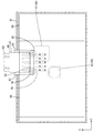
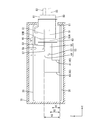
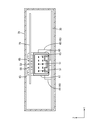
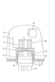
- the electrical junction box 10 includes a first substrate 20, a second substrate 30 disposed to face the first substrate 20, a heat generating component 40 mounted on the second substrate 30, and
- the second substrate 30 has a rectangular shape that is fitted inside the case 70, and is configured by overlapping a printed circuit board and a bus bar.
- a conductive path made of a copper foil or the like is formed on an insulating plate made of an insulating material by a printed wiring technique.
- the bus bar is formed by punching a metal plate material made of a copper alloy or the like according to the shape of the conductive path.
- the printed circuit board has a plurality of component insertion holes for connecting electronic components to the bus bar.
- the heat generating component 40 is electrically connected to a conductive path provided on the second substrate 30 (printed substrate) by a known method such as soldering.
- the heat generating component 40 includes a switching element such as an FET (Field-Effect-Transistor), a coil 41 described later, an electrolytic capacitor 43, and the like. Note that illustration of the heat generating components other than the coil 41 and the electrolytic capacitor 43 is omitted.
- the first substrate 20 has a smaller area than the second substrate 30 and is placed in the case 70 in a posture parallel to the second substrate 30 with a predetermined interval in the vertical direction. Contained.
- the first substrate 20 has a rectangular shape, and a conductive path made of copper foil or the like is printed on an insulating plate made of an insulating material.
- An electronic component is mounted on the conductive path, and a current flowing through the second substrate 30 It is a control board for controlling the above.
- the second substrate 30 is provided with a through hole through which the terminal 50 is inserted and connected. Further, the conductive paths between the first substrate 20 and the second substrate 30 are connected by a plurality of connection terminals or the like.
- the heat generating component 40 indicates an electronic component that generates heat when energized.
- Examples of the heat generating component 40 include an electronic component that generates a relatively large amount of heat and an electronic component that does not have sufficient heat dissipation performance because it is difficult to directly contact the bus bar.
- the coil 41 has a rectangular shape in plan view, and its vertical (vertical) dimension (height dimension) H1 with respect to the second substrate 30 is a lower terminal described later. It is smaller than the dimension H ⁇ b> 2 between the parallel part 55 of 50 ⁇ / b> A and the second substrate 30.
- the electrolytic capacitor 43 has a shape in which a cylindrical main body portion rides on a plate-like connection portion having a rectangular shape in plan view.
- the electrolytic capacitor 43 has a vertical dimension (height dimension) H3 larger than the vertical dimension H1 of the coil 41, and is located between the parallel portion 55 of the lower terminal 50A and the second substrate 30. It is larger than the dimension H2.
- a total of ten terminals 50 are used, two in the vertical direction and five in the horizontal direction (width direction).
- the terminal 50 is formed by bending a rod-shaped conductive member into an L shape.
- the terminal 50 is for flowing a control signal current to the second substrate 30 which is a control substrate. Since a large current does not flow, the terminal 50 is relatively thin.
- the terminal 50 includes a counterpart connection part 51 and an extension part 53.
- the extending portion 53 includes a parallel portion 55, a bent portion 57, and a connecting portion 59.
- the mating side connecting portion 51 protrudes forward (in the fitting direction with the mating connector housing 81) from a terminal holding portion 63 of the connector housing 60 described later, and is connected to the mating terminal.
- the parallel part 55 protrudes rearward from the terminal holding part 63 (on the side opposite to the fitting direction with the mating connector housing 81) and extends in parallel with the second substrate 30.
- the bent portion 57 is formed by bending the parallel portion 55 extending in the front-rear direction to the first substrate 20 side (upper side) at a right angle, thereby making the entire terminal 50 L-shaped.
- the connecting portion 59 extends from the bent portion 57 to the first substrate 20 side (upper side), passes through a through hole provided in the first substrate 20, protrudes to the upper surface side of the first substrate 20, and is connected to the first substrate 20. It is connected to the conductive path by soldering or the like.
- a connector housing 60 is fixed to the first board 20 by screws 65 with screws 65.
- the connector housing 60 is made of a synthetic resin, and includes a square hood portion 61 in which a mating connector housing 81 can be fitted, and a terminal holding portion 63 that is provided at the rear end portion of the hood portion 61 and holds the terminal 50. ing.
- the hood portion 61 is open forward and has an inner shape that follows the outer shape of the mating connector housing 81.
- the case 70 has a rectangular box shape in plan view as shown in FIGS.
- the case 70 includes a synthetic resin holding member that holds the first substrate 20 and the second substrate 30, and a metal shield cover that is mounted on the holding member.
- An opening is provided in a part of the case 70, and the connector housing 60 is arranged in the opening.
- the mating connector 80 includes a mating terminal connected to the mating side connection portion 51 of the terminal 50 and a mating connector housing 81.
- An electric wire 83 is connected to the mating terminal and is pulled out from the rear of the mating connector housing 81.
- the electrical junction box 10 of the present embodiment is configured as described above, and the assembly method and operation thereof will be described subsequently.
- the second substrate 30 is accommodated and fixed in the case 70.
- the heat generating components 40 such as the coil 41 and the electrolytic capacitor 43 are mounted on the second substrate 30.
- the connector housing 60 and the terminals 50 are attached to the first substrate 20.
- the connector housing 60 holding the terminals 50 is disposed at a predetermined position on the lower surface of the first substrate 20, and the connection portions 59 of the terminals 50 are inserted through the through holes of the first substrate 20 and connected.
- the connector housing 60 holds the terminal 50 in a state in which the extended portion 53 of the terminal 50 is exposed on the rear side of the terminal holding portion 63.
- the connector housing 60 is fixed to the first substrate 20 with screws 65.
- the first substrate 20 to which the connector housing 60 is attached is disposed at a predetermined position above the second substrate 30. While the first substrate 20 and the second substrate 30 are connected by the connection terminals, the first substrate 20 is fixed to the case 70 and positioned. In this state, the extending portion 53 is disposed in the vicinity of the heat generating component 40. More specifically, the parallel portion 55 of the terminal 50 is located above the coil 41. That is, the coil 41 is disposed between the parallel part 55 and the second substrate 30. Further, the connection portion 59 of the terminal 50 is located at a position adjacent to the electrolytic capacitor 43.
- the vicinity of the heat generating component 40 refers to a range in which the heat of the heat generating component 40 is transmitted to the extending portion 53 of the terminal 50, and when it is adjacent to the heat generating component 40 or above and below the heat generating component 40. It is desirable that it is close to the extent that it does not interfere with each other during assembly.
- adjacent to the heat generating component 40 refers to the vicinity not including the top and bottom of the heat generating component 40.
- the heat generating component 40 is disposed in the vicinity of the extending portion 53 of the terminal 50, so that the heat generated by the heat generating component 40 is connected to the first substrate 20 and the terminal 50 via the terminal 50. Heat is transmitted to the electric wire 83 through the wire and is radiated.
- the first substrate 20 and the electric wire 83 were originally not in the vicinity of the heat generating component 40 and did not contribute much to the heat dissipation. However, heat is transferred to the first substrate 20 and the electric wire 83 via the terminal 50, so that the heat is dissipated. Will be able to contribute.
- the terminal 50 is for flowing a control signal current, and since the amount of current that the terminal 50 itself generates heat does not flow to the terminal 50, the terminal 50 has a surrounding heat (heat from the heat generating component 40). Can be absorbed. Further, by arranging the heat generating component 40 having a small vertical dimension like the coil 41 under the terminal 50, a dead space can be used and the electrical junction box 10 can be downsized.
- the heat generating component 40 is mounted in the vicinity of the extending portion 53 of the terminal 50. Therefore, the heat generated in the heat generating component 40 can be released to the first substrate 20 to which the terminal 50 is connected via the extending portion 53 of the terminal 50. Further, when mating with the mating connector 80, heat can also be radiated to the mating connector 80 side via the terminals 50. And since the terminal 50 exists in the vicinity of the heat-emitting component 40, the heat of the heat-generating component 40 can be radiated intensively. Further, since the heat radiation amount is improved, electronic components can be arranged at high density. Furthermore, since the heat generating component 40 is arranged in the vicinity of the extending portion 53 of the terminal 50, the heat radiation efficiency can be increased at a low cost.
- a wall portion 67 is provided on the connector housing 60, and the wall portion 67 extends from the connector housing 60 toward the vicinity of the heat generating component 40. More specifically, the electrolytic capacitor 43 is disposed between the wall portions 67. Since the configuration other than the above is substantially the same as that of the first embodiment, the same members are denoted by the same reference numerals, and redundant description is omitted.
- a wall portion 67 separate from the connector housing 60 is attached to the rear end portion of the connector housing 60.
- a pair of wall portions 67 are provided in the width direction so as to sandwich the electrolytic capacitor 43 therebetween.
- the wall portion 67 extends rearward from the rear end portion of the connector housing 60 and is bent inward in the width direction after passing through the side of the electrolytic capacitor 43.
- the terminals 50 are arranged in two upper and lower stages, but may be arranged in one or more stages.
- the terminal 50 is used to flow a control signal current, but it may be a terminal for other purposes.
- the terminal 50 is L-shaped bent by the bent portion 57, but may have other shapes.
- the heat generating component 40 is disposed in the vicinity of the terminal 50.
- the heat generating component 40 may be disposed at a position where the heat generating component 40 contacts the terminal 50.
- the first substrate 20 is the control substrate and the second substrate 30 is the substrate on which the conductive path is formed.
- the first substrate is the substrate on which the conductive path is formed, and the second substrate is A control board may be used. That is, the heat of the heat generating component on the control board may be transferred by the connector terminal of the power supply circuit.
- the first substrate 20 is disposed above the second substrate 30, but the first substrate 20 may be disposed below the second substrate 30.
- the connector housing 60 is fixed to the first substrate 20, but may be fixed to the second substrate side.
- a pair of wall portions 67 are provided so as to place the heat generating component 40 therebetween, but one wall portion 67 may be provided as long as it is disposed in the vicinity of the heat generating component 40, Multiple may be used.
- the terminal 50 of the connector housing 60 is configured to pass through a through hole provided in the first substrate 20 and be connected to the conductive path of the first substrate 20 by soldering or the like.
- the terminal of the connector housing 60 may be configured to be connected to a conductive path provided on the first substrate 20 or the second substrate 30 by a known method such as reflow soldering (so-called surface mounting). Good.
Landscapes
- Engineering & Computer Science (AREA)
- Microelectronics & Electronic Packaging (AREA)
- Power Engineering (AREA)
- Architecture (AREA)
- Civil Engineering (AREA)
- Structural Engineering (AREA)
- Physics & Mathematics (AREA)
- Thermal Sciences (AREA)
- Connection Or Junction Boxes (AREA)
- Cooling Or The Like Of Electrical Apparatus (AREA)
Priority Applications (2)
| Application Number | Priority Date | Filing Date | Title |
|---|---|---|---|
| CN201780050166.6A CN109643884B (zh) | 2016-08-22 | 2017-08-08 | 电接线箱 |
| US16/327,048 US10763048B2 (en) | 2016-08-22 | 2017-08-08 | Electrical junction box |
Applications Claiming Priority (2)
| Application Number | Priority Date | Filing Date | Title |
|---|---|---|---|
| JP2016161757A JP6620941B2 (ja) | 2016-08-22 | 2016-08-22 | 電気接続箱 |
| JP2016-161757 | 2016-08-22 |
Publications (1)
| Publication Number | Publication Date |
|---|---|
| WO2018037905A1 true WO2018037905A1 (ja) | 2018-03-01 |
Family
ID=61246598
Family Applications (1)
| Application Number | Title | Priority Date | Filing Date |
|---|---|---|---|
| PCT/JP2017/028708 WO2018037905A1 (ja) | 2016-08-22 | 2017-08-08 | 電気接続箱 |
Country Status (4)
| Country | Link |
|---|---|
| US (1) | US10763048B2 (zh) |
| JP (1) | JP6620941B2 (zh) |
| CN (1) | CN109643884B (zh) |
| WO (1) | WO2018037905A1 (zh) |
Families Citing this family (1)
| Publication number | Priority date | Publication date | Assignee | Title |
|---|---|---|---|---|
| JP6785261B2 (ja) | 2018-05-11 | 2020-11-18 | 矢崎総業株式会社 | コネクタユニット |
Citations (5)
| Publication number | Priority date | Publication date | Assignee | Title |
|---|---|---|---|---|
| JP2007242567A (ja) * | 2006-03-10 | 2007-09-20 | Furukawa Electric Co Ltd:The | 回路基板構造及び電気接続箱 |
| JP2008147253A (ja) * | 2006-12-06 | 2008-06-26 | Auto Network Gijutsu Kenkyusho:Kk | プリント基板装置 |
| JP2009081180A (ja) * | 2007-09-25 | 2009-04-16 | Denso Corp | 回路装置 |
| JP2013038948A (ja) * | 2011-08-09 | 2013-02-21 | Auto Network Gijutsu Kenkyusho:Kk | 回路構成体及び電気接続箱 |
| JP2014166089A (ja) * | 2013-02-27 | 2014-09-08 | Auto Network Gijutsu Kenkyusho:Kk | 電気接続箱 |
Family Cites Families (13)
| Publication number | Priority date | Publication date | Assignee | Title |
|---|---|---|---|---|
| JP2973792B2 (ja) * | 1993-09-21 | 1999-11-08 | 富士電機株式会社 | 樹脂封止形半導体装置 |
| JPH08148801A (ja) * | 1994-11-24 | 1996-06-07 | Fujitsu Denso Ltd | 半導体素子の基板上実装方法と基板上実装装置 |
| US6700795B1 (en) * | 2002-01-23 | 2004-03-02 | Yazaki North America | Scalable, modular architecture for automotive power distribution and body control functions |
| KR100759550B1 (ko) * | 2005-01-20 | 2007-09-18 | 삼성에스디아이 주식회사 | 디스플레이 모듈 |
| JP2009129778A (ja) * | 2007-11-26 | 2009-06-11 | Sumitomo Wiring Syst Ltd | 基板用コネクタ及び電気接続箱 |
| JP2013103535A (ja) * | 2011-11-10 | 2013-05-30 | Honda Elesys Co Ltd | 電動パワーステアリング用電子制御ユニット |
| JP5855046B2 (ja) * | 2013-04-26 | 2016-02-09 | 古河電気工業株式会社 | 電気接続箱 |
| JP5995147B2 (ja) * | 2013-09-24 | 2016-09-21 | 住友電装株式会社 | 回路構成体 |
| US10014675B2 (en) * | 2014-06-19 | 2018-07-03 | Autonetworks Technologies, Ltd. | Electrical junction box and connector housing |
| CN204928015U (zh) * | 2015-09-28 | 2015-12-30 | 东风汽车股份有限公司 | 带有直流接触器的电动汽车高压转接盒 |
| CN105810664B (zh) * | 2016-04-07 | 2018-06-01 | 上海华力微电子有限公司 | 测试金属线的电迁移结构 |
| US20190123522A1 (en) * | 2017-10-23 | 2019-04-25 | Lear Corporation | Electrical unit |
| JP6626066B2 (ja) * | 2017-11-01 | 2019-12-25 | 矢崎総業株式会社 | 電気接続箱 |
-
2016
- 2016-08-22 JP JP2016161757A patent/JP6620941B2/ja active Active
-
2017
- 2017-08-08 CN CN201780050166.6A patent/CN109643884B/zh active Active
- 2017-08-08 WO PCT/JP2017/028708 patent/WO2018037905A1/ja active Application Filing
- 2017-08-08 US US16/327,048 patent/US10763048B2/en active Active
Patent Citations (5)
| Publication number | Priority date | Publication date | Assignee | Title |
|---|---|---|---|---|
| JP2007242567A (ja) * | 2006-03-10 | 2007-09-20 | Furukawa Electric Co Ltd:The | 回路基板構造及び電気接続箱 |
| JP2008147253A (ja) * | 2006-12-06 | 2008-06-26 | Auto Network Gijutsu Kenkyusho:Kk | プリント基板装置 |
| JP2009081180A (ja) * | 2007-09-25 | 2009-04-16 | Denso Corp | 回路装置 |
| JP2013038948A (ja) * | 2011-08-09 | 2013-02-21 | Auto Network Gijutsu Kenkyusho:Kk | 回路構成体及び電気接続箱 |
| JP2014166089A (ja) * | 2013-02-27 | 2014-09-08 | Auto Network Gijutsu Kenkyusho:Kk | 電気接続箱 |
Also Published As
| Publication number | Publication date |
|---|---|
| CN109643884A (zh) | 2019-04-16 |
| JP2018033196A (ja) | 2018-03-01 |
| US20190189360A1 (en) | 2019-06-20 |
| US10763048B2 (en) | 2020-09-01 |
| JP6620941B2 (ja) | 2019-12-18 |
| CN109643884B (zh) | 2020-07-10 |
Similar Documents
| Publication | Publication Date | Title |
|---|---|---|
| JP7001960B2 (ja) | 回路構成体 | |
| CN108702856B (zh) | 电路构成体 | |
| JP5995113B2 (ja) | 電気接続箱 | |
| JP4387314B2 (ja) | 電気接続箱 | |
| WO2015194666A1 (ja) | 電気接続箱及びコネクタハウジング | |
| WO2016111143A1 (ja) | 蓄電ユニット | |
| CN108293311B (zh) | 电气接线盒 | |
| JP2005304105A (ja) | 電気接続箱 | |
| CN110383612B (zh) | 电气连接箱 | |
| JP2016152349A (ja) | 回路構成体 | |
| JP2006060924A (ja) | 電気接続箱 | |
| JP2012165567A (ja) | 電気接続箱 | |
| WO2016002749A1 (ja) | 電気接続箱 | |
| JP2020127302A (ja) | 電気接続箱 | |
| JP6620941B2 (ja) | 電気接続箱 | |
| JP5561521B2 (ja) | 電気接続箱 | |
| JP2007259539A (ja) | 車載用電気接続箱 | |
| JP2006187122A (ja) | 回路構成体 | |
| WO2020017471A1 (ja) | 回路基板 | |
| JP2006100553A (ja) | 回路構成体 | |
| JP5545491B2 (ja) | 回路構成体 | |
| WO2017098899A1 (ja) | 電気接続箱 | |
| JP5187103B2 (ja) | 電気接続箱 | |
| JP2006288117A (ja) | スイッチングユニット | |
| JP2006310557A (ja) | スイッチングユニット |
Legal Events
| Date | Code | Title | Description |
|---|---|---|---|
| 121 | Ep: the epo has been informed by wipo that ep was designated in this application |
Ref document number: 17843390 Country of ref document: EP Kind code of ref document: A1 |
|
| NENP | Non-entry into the national phase |
Ref country code: DE |
|
| 122 | Ep: pct application non-entry in european phase |
Ref document number: 17843390 Country of ref document: EP Kind code of ref document: A1 |