WO2018037905A1 - Electrical junction box - Google Patents
Electrical junction box Download PDFInfo
- Publication number
- WO2018037905A1 WO2018037905A1 PCT/JP2017/028708 JP2017028708W WO2018037905A1 WO 2018037905 A1 WO2018037905 A1 WO 2018037905A1 JP 2017028708 W JP2017028708 W JP 2017028708W WO 2018037905 A1 WO2018037905 A1 WO 2018037905A1
- Authority
- WO
- WIPO (PCT)
- Prior art keywords
- substrate
- terminal
- connector housing
- heat
- parallel
- Prior art date
Links
Images

Classifications
-
- H—ELECTRICITY
- H02—GENERATION; CONVERSION OR DISTRIBUTION OF ELECTRIC POWER
- H02G—INSTALLATION OF ELECTRIC CABLES OR LINES, OR OF COMBINED OPTICAL AND ELECTRIC CABLES OR LINES
- H02G3/00—Installations of electric cables or lines or protective tubing therefor in or on buildings, equivalent structures or vehicles
- H02G3/02—Details
- H02G3/08—Distribution boxes; Connection or junction boxes
- H02G3/081—Bases, casings or covers
-
- H—ELECTRICITY
- H01—ELECTRIC ELEMENTS
- H01G—CAPACITORS; CAPACITORS, RECTIFIERS, DETECTORS, SWITCHING DEVICES OR LIGHT-SENSITIVE DEVICES, OF THE ELECTROLYTIC TYPE
- H01G9/00—Electrolytic capacitors, rectifiers, detectors, switching devices, light-sensitive or temperature-sensitive devices; Processes of their manufacture
- H01G9/004—Details
- H01G9/08—Housing; Encapsulation
-
- H—ELECTRICITY
- H01—ELECTRIC ELEMENTS
- H01G—CAPACITORS; CAPACITORS, RECTIFIERS, DETECTORS, SWITCHING DEVICES OR LIGHT-SENSITIVE DEVICES, OF THE ELECTROLYTIC TYPE
- H01G9/00—Electrolytic capacitors, rectifiers, detectors, switching devices, light-sensitive or temperature-sensitive devices; Processes of their manufacture
- H01G9/0003—Protection against electric or thermal overload; cooling arrangements; means for avoiding the formation of cathode films
-
- H—ELECTRICITY
- H02—GENERATION; CONVERSION OR DISTRIBUTION OF ELECTRIC POWER
- H02G—INSTALLATION OF ELECTRIC CABLES OR LINES, OR OF COMBINED OPTICAL AND ELECTRIC CABLES OR LINES
- H02G3/00—Installations of electric cables or lines or protective tubing therefor in or on buildings, equivalent structures or vehicles
- H02G3/02—Details
- H02G3/08—Distribution boxes; Connection or junction boxes
-
- H—ELECTRICITY
- H05—ELECTRIC TECHNIQUES NOT OTHERWISE PROVIDED FOR
- H05K—PRINTED CIRCUITS; CASINGS OR CONSTRUCTIONAL DETAILS OF ELECTRIC APPARATUS; MANUFACTURE OF ASSEMBLAGES OF ELECTRICAL COMPONENTS
- H05K1/00—Printed circuits
- H05K1/16—Printed circuits incorporating printed electric components, e.g. printed resistor, capacitor, inductor
- H05K1/162—Printed circuits incorporating printed electric components, e.g. printed resistor, capacitor, inductor incorporating printed capacitors
-
- H—ELECTRICITY
- H05—ELECTRIC TECHNIQUES NOT OTHERWISE PROVIDED FOR
- H05K—PRINTED CIRCUITS; CASINGS OR CONSTRUCTIONAL DETAILS OF ELECTRIC APPARATUS; MANUFACTURE OF ASSEMBLAGES OF ELECTRICAL COMPONENTS
- H05K7/00—Constructional details common to different types of electric apparatus
- H05K7/20—Modifications to facilitate cooling, ventilating, or heating
-
- H—ELECTRICITY
- H01—ELECTRIC ELEMENTS
- H01G—CAPACITORS; CAPACITORS, RECTIFIERS, DETECTORS, SWITCHING DEVICES OR LIGHT-SENSITIVE DEVICES, OF THE ELECTROLYTIC TYPE
- H01G9/00—Electrolytic capacitors, rectifiers, detectors, switching devices, light-sensitive or temperature-sensitive devices; Processes of their manufacture
- H01G9/28—Structural combinations of electrolytic capacitors, rectifiers, detectors, switching devices with other electric components not covered by this subclass
-
- Y—GENERAL TAGGING OF NEW TECHNOLOGICAL DEVELOPMENTS; GENERAL TAGGING OF CROSS-SECTIONAL TECHNOLOGIES SPANNING OVER SEVERAL SECTIONS OF THE IPC; TECHNICAL SUBJECTS COVERED BY FORMER USPC CROSS-REFERENCE ART COLLECTIONS [XRACs] AND DIGESTS
- Y02—TECHNOLOGIES OR APPLICATIONS FOR MITIGATION OR ADAPTATION AGAINST CLIMATE CHANGE
- Y02T—CLIMATE CHANGE MITIGATION TECHNOLOGIES RELATED TO TRANSPORTATION
- Y02T10/00—Road transport of goods or passengers
- Y02T10/60—Other road transportation technologies with climate change mitigation effect
- Y02T10/70—Energy storage systems for electromobility, e.g. batteries
Definitions
- the present invention relates to an electrical junction box.
- an electric connection box in which a power distribution circuit is constituted by a plurality of bus bars and a switch element or the like is incorporated is generally known.
- a circuit structure housed in these electrical junction boxes there is a circuit structure described in Japanese Patent Application Laid-Open No. 2005-151617 (Patent Document 1 below).
- Patent Document 1 Japanese Patent Application Laid-Open No. 2005-151617
- a circuit board and a heat radiating member that radiates heat of the circuit board to the outside are overlapped.
- a boss portion protruding so as to be close to the component is provided on the case or the cover, and an insulating heat transfer member is provided on the boss portion.
- a structure for transferring the heat of a component to a case or a cover by applying is disclosed. Furthermore, in this control device, a convex surface close to the terminal is provided on the case or cover, and the heat of the case or cover is applied to the convex surface by applying a heat transfer member to the wire. Heat is transferred to the harness.
- An electrical connection box disclosed in the present specification includes a connector housing that fits into a mating connector housing, a terminal that is held by a terminal holding portion provided in the connector housing, and the terminal holding portion out of the terminals.
- the first board mounted to the end part on the extension part side extending to the opposite side of the mating connector housing, and the second board facing the first board And a heat generating component disposed at a position in contact with the extending portion or in the vicinity of the extending portion.
- the heat generating component is mounted at a position in contact with the extension portion of the terminal or in the vicinity of the extension portion. Therefore, the heat generated in the heat generating component can be released to the first substrate to which the terminal is connected via the terminal extension. Moreover, at the time of fitting with the mating connector, heat can be released from the electric wire connected to the mating terminal via the terminal. And since there is a terminal in the vicinity of the heat generating component, the heat of the heat generating component can be radiated in a concentrated manner. Further, since the heat radiation amount is improved, electronic components can be arranged at high density. Further, since the heat generating component is arranged at a position in contact with the extended portion of the terminal or in the vicinity of the extended portion of the terminal, the heat radiation efficiency can be increased at a low cost.
- a wall portion may extend from the connector housing toward the vicinity of the heat generating component.
- heat is transmitted to the connector housing through the wall portion, and heat can be radiated through the connector housing, so that heat can be further radiated.
- the extending portion includes a parallel portion parallel to the second substrate, a bent portion bent from the parallel portion toward the first substrate, and the first substrate extending from the bent portion toward the first substrate.
- the heat generating component is an electrolytic capacitor having a dimension in a direction perpendicular to the second substrate that is larger than a dimension between the second substrate and the parallel part, It is good also as a structure mounted in the position adjacent to the said connection part.
- the extending portion includes a parallel portion parallel to the second substrate, a bent portion bent from the parallel portion toward the first substrate, and the first substrate extending from the bent portion toward the first substrate.
- the heat generating component is a coil having a dimension in a direction perpendicular to the second substrate smaller than a dimension between the second substrate and the parallel portion, It is good also as a structure mounted between the parallel part and the said 2nd board
- the heat of the heat generating component can be radiated.
- Embodiment 1 will be described with reference to FIGS. 1 to 4.
- the electric junction box 10 is arranged in a power supply path between a power source such as a battery of a vehicle such as an electric vehicle or a hybrid vehicle and a load including an in-vehicle electrical component such as a lamp or a drive motor, for example, a DC-DC converter. It can be used for inverters and the like.
- a power source such as a battery of a vehicle such as an electric vehicle or a hybrid vehicle
- a load including an in-vehicle electrical component such as a lamp or a drive motor, for example, a DC-DC converter. It can be used for inverters and the like.
- the vertical (Z-axis) direction and the left-right (Y-axis) direction will be described with reference to the direction of FIG. 3, and the front-rear (X-axis) direction will be described with the right side of FIG. .
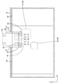
- the electrical junction box 10 includes a first substrate 20, a second substrate 30 disposed to face the first substrate 20, a heat generating component 40 mounted on the second substrate 30, and
- the second substrate 30 has a rectangular shape that is fitted inside the case 70, and is configured by overlapping a printed circuit board and a bus bar.
- a conductive path made of a copper foil or the like is formed on an insulating plate made of an insulating material by a printed wiring technique.
- the bus bar is formed by punching a metal plate material made of a copper alloy or the like according to the shape of the conductive path.
- the printed circuit board has a plurality of component insertion holes for connecting electronic components to the bus bar.
- the heat generating component 40 is electrically connected to a conductive path provided on the second substrate 30 (printed substrate) by a known method such as soldering.
- the heat generating component 40 includes a switching element such as an FET (Field-Effect-Transistor), a coil 41 described later, an electrolytic capacitor 43, and the like. Note that illustration of the heat generating components other than the coil 41 and the electrolytic capacitor 43 is omitted.
- the first substrate 20 has a smaller area than the second substrate 30 and is placed in the case 70 in a posture parallel to the second substrate 30 with a predetermined interval in the vertical direction. Contained.
- the first substrate 20 has a rectangular shape, and a conductive path made of copper foil or the like is printed on an insulating plate made of an insulating material.
- An electronic component is mounted on the conductive path, and a current flowing through the second substrate 30 It is a control board for controlling the above.
- the second substrate 30 is provided with a through hole through which the terminal 50 is inserted and connected. Further, the conductive paths between the first substrate 20 and the second substrate 30 are connected by a plurality of connection terminals or the like.
- the heat generating component 40 indicates an electronic component that generates heat when energized.
- Examples of the heat generating component 40 include an electronic component that generates a relatively large amount of heat and an electronic component that does not have sufficient heat dissipation performance because it is difficult to directly contact the bus bar.
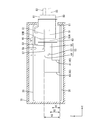
- the coil 41 has a rectangular shape in plan view, and its vertical (vertical) dimension (height dimension) H1 with respect to the second substrate 30 is a lower terminal described later. It is smaller than the dimension H ⁇ b> 2 between the parallel part 55 of 50 ⁇ / b> A and the second substrate 30.
- the electrolytic capacitor 43 has a shape in which a cylindrical main body portion rides on a plate-like connection portion having a rectangular shape in plan view.
- the electrolytic capacitor 43 has a vertical dimension (height dimension) H3 larger than the vertical dimension H1 of the coil 41, and is located between the parallel portion 55 of the lower terminal 50A and the second substrate 30. It is larger than the dimension H2.
- a total of ten terminals 50 are used, two in the vertical direction and five in the horizontal direction (width direction).
- the terminal 50 is formed by bending a rod-shaped conductive member into an L shape.
- the terminal 50 is for flowing a control signal current to the second substrate 30 which is a control substrate. Since a large current does not flow, the terminal 50 is relatively thin.
- the terminal 50 includes a counterpart connection part 51 and an extension part 53.
- the extending portion 53 includes a parallel portion 55, a bent portion 57, and a connecting portion 59.
- the mating side connecting portion 51 protrudes forward (in the fitting direction with the mating connector housing 81) from a terminal holding portion 63 of the connector housing 60 described later, and is connected to the mating terminal.
- the parallel part 55 protrudes rearward from the terminal holding part 63 (on the side opposite to the fitting direction with the mating connector housing 81) and extends in parallel with the second substrate 30.
- the bent portion 57 is formed by bending the parallel portion 55 extending in the front-rear direction to the first substrate 20 side (upper side) at a right angle, thereby making the entire terminal 50 L-shaped.
- the connecting portion 59 extends from the bent portion 57 to the first substrate 20 side (upper side), passes through a through hole provided in the first substrate 20, protrudes to the upper surface side of the first substrate 20, and is connected to the first substrate 20. It is connected to the conductive path by soldering or the like.
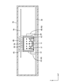
- a connector housing 60 is fixed to the first board 20 by screws 65 with screws 65.
- the connector housing 60 is made of a synthetic resin, and includes a square hood portion 61 in which a mating connector housing 81 can be fitted, and a terminal holding portion 63 that is provided at the rear end portion of the hood portion 61 and holds the terminal 50. ing.
- the hood portion 61 is open forward and has an inner shape that follows the outer shape of the mating connector housing 81.
- the case 70 has a rectangular box shape in plan view as shown in FIGS.
- the case 70 includes a synthetic resin holding member that holds the first substrate 20 and the second substrate 30, and a metal shield cover that is mounted on the holding member.
- An opening is provided in a part of the case 70, and the connector housing 60 is arranged in the opening.
- the mating connector 80 includes a mating terminal connected to the mating side connection portion 51 of the terminal 50 and a mating connector housing 81.
- An electric wire 83 is connected to the mating terminal and is pulled out from the rear of the mating connector housing 81.
- the electrical junction box 10 of the present embodiment is configured as described above, and the assembly method and operation thereof will be described subsequently.
- the second substrate 30 is accommodated and fixed in the case 70.
- the heat generating components 40 such as the coil 41 and the electrolytic capacitor 43 are mounted on the second substrate 30.
- the connector housing 60 and the terminals 50 are attached to the first substrate 20.
- the connector housing 60 holding the terminals 50 is disposed at a predetermined position on the lower surface of the first substrate 20, and the connection portions 59 of the terminals 50 are inserted through the through holes of the first substrate 20 and connected.
- the connector housing 60 holds the terminal 50 in a state in which the extended portion 53 of the terminal 50 is exposed on the rear side of the terminal holding portion 63.
- the connector housing 60 is fixed to the first substrate 20 with screws 65.
- the first substrate 20 to which the connector housing 60 is attached is disposed at a predetermined position above the second substrate 30. While the first substrate 20 and the second substrate 30 are connected by the connection terminals, the first substrate 20 is fixed to the case 70 and positioned. In this state, the extending portion 53 is disposed in the vicinity of the heat generating component 40. More specifically, the parallel portion 55 of the terminal 50 is located above the coil 41. That is, the coil 41 is disposed between the parallel part 55 and the second substrate 30. Further, the connection portion 59 of the terminal 50 is located at a position adjacent to the electrolytic capacitor 43.
- the vicinity of the heat generating component 40 refers to a range in which the heat of the heat generating component 40 is transmitted to the extending portion 53 of the terminal 50, and when it is adjacent to the heat generating component 40 or above and below the heat generating component 40. It is desirable that it is close to the extent that it does not interfere with each other during assembly.
- adjacent to the heat generating component 40 refers to the vicinity not including the top and bottom of the heat generating component 40.
- the heat generating component 40 is disposed in the vicinity of the extending portion 53 of the terminal 50, so that the heat generated by the heat generating component 40 is connected to the first substrate 20 and the terminal 50 via the terminal 50. Heat is transmitted to the electric wire 83 through the wire and is radiated.
- the first substrate 20 and the electric wire 83 were originally not in the vicinity of the heat generating component 40 and did not contribute much to the heat dissipation. However, heat is transferred to the first substrate 20 and the electric wire 83 via the terminal 50, so that the heat is dissipated. Will be able to contribute.
- the terminal 50 is for flowing a control signal current, and since the amount of current that the terminal 50 itself generates heat does not flow to the terminal 50, the terminal 50 has a surrounding heat (heat from the heat generating component 40). Can be absorbed. Further, by arranging the heat generating component 40 having a small vertical dimension like the coil 41 under the terminal 50, a dead space can be used and the electrical junction box 10 can be downsized.
- the heat generating component 40 is mounted in the vicinity of the extending portion 53 of the terminal 50. Therefore, the heat generated in the heat generating component 40 can be released to the first substrate 20 to which the terminal 50 is connected via the extending portion 53 of the terminal 50. Further, when mating with the mating connector 80, heat can also be radiated to the mating connector 80 side via the terminals 50. And since the terminal 50 exists in the vicinity of the heat-emitting component 40, the heat of the heat-generating component 40 can be radiated intensively. Further, since the heat radiation amount is improved, electronic components can be arranged at high density. Furthermore, since the heat generating component 40 is arranged in the vicinity of the extending portion 53 of the terminal 50, the heat radiation efficiency can be increased at a low cost.
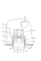
- a wall portion 67 is provided on the connector housing 60, and the wall portion 67 extends from the connector housing 60 toward the vicinity of the heat generating component 40. More specifically, the electrolytic capacitor 43 is disposed between the wall portions 67. Since the configuration other than the above is substantially the same as that of the first embodiment, the same members are denoted by the same reference numerals, and redundant description is omitted.
- a wall portion 67 separate from the connector housing 60 is attached to the rear end portion of the connector housing 60.
- a pair of wall portions 67 are provided in the width direction so as to sandwich the electrolytic capacitor 43 therebetween.
- the wall portion 67 extends rearward from the rear end portion of the connector housing 60 and is bent inward in the width direction after passing through the side of the electrolytic capacitor 43.
- the terminals 50 are arranged in two upper and lower stages, but may be arranged in one or more stages.
- the terminal 50 is used to flow a control signal current, but it may be a terminal for other purposes.
- the terminal 50 is L-shaped bent by the bent portion 57, but may have other shapes.
- the heat generating component 40 is disposed in the vicinity of the terminal 50.
- the heat generating component 40 may be disposed at a position where the heat generating component 40 contacts the terminal 50.
- the first substrate 20 is the control substrate and the second substrate 30 is the substrate on which the conductive path is formed.
- the first substrate is the substrate on which the conductive path is formed, and the second substrate is A control board may be used. That is, the heat of the heat generating component on the control board may be transferred by the connector terminal of the power supply circuit.
- the first substrate 20 is disposed above the second substrate 30, but the first substrate 20 may be disposed below the second substrate 30.
- the connector housing 60 is fixed to the first substrate 20, but may be fixed to the second substrate side.
- a pair of wall portions 67 are provided so as to place the heat generating component 40 therebetween, but one wall portion 67 may be provided as long as it is disposed in the vicinity of the heat generating component 40, Multiple may be used.
- the terminal 50 of the connector housing 60 is configured to pass through a through hole provided in the first substrate 20 and be connected to the conductive path of the first substrate 20 by soldering or the like.
- the terminal of the connector housing 60 may be configured to be connected to a conductive path provided on the first substrate 20 or the second substrate 30 by a known method such as reflow soldering (so-called surface mounting). Good.
Abstract
An electrical junction box 10 provided with: a connector housing 60 that engages with a counterpart connector housing 81; a terminal 50 that is held by a terminal holding unit 63 provided on the connector housing 60; a first substrate 20 that is connected with the end part near an extension part 53 extended to the side of the terminal 50 in reverse to the engagement direction from the terminal holding unit 63; a second substrate 30 facing opposite the first substrate 20; and a heat generating part mounted on the second substrate 30 and arranged in the vicinity of the extension part 53.
Description
本発明は、電気接続箱に関する。
The present invention relates to an electrical junction box.
従来、共通の車載電源から各電子ユニットに電力を分配する手段として、複数本のバスバーにより配電用回路を構成し、これにスイッチ素子等を組み込んだ電気接続箱が一般に知られている。これらの電気接続箱に収容される回路構成体の一例として、特開2005-151617号公報(下記特許文献1)に記載の回路構成体がある。この回路構成体では、回路基板とこの回路基板の熱を外部に放熱する放熱部材とが重ねられている。
Conventionally, as a means for distributing electric power from a common in-vehicle power source to each electronic unit, an electric connection box in which a power distribution circuit is constituted by a plurality of bus bars and a switch element or the like is incorporated is generally known. As an example of a circuit structure housed in these electrical junction boxes, there is a circuit structure described in Japanese Patent Application Laid-Open No. 2005-151617 (Patent Document 1 below). In this circuit structure, a circuit board and a heat radiating member that radiates heat of the circuit board to the outside are overlapped.
ところで、回路基板に配置された素子によっては、発熱量が多いものがある。このような発熱量の多い電子部品(発熱部品)の近傍では、より多くの熱を集中的に放熱する必要がある。しかしながら、特開2005-151617号公報(下記特許文献1)に記載の従来の回路構成体では、放熱部材は、回路基板全体に重ねられており、全体としての熱を逃すことはできる一方で、集中的に、基板内の特定箇所を放熱することができない。そこで、特開2010-180702号公報(下記特許文献2)に記載の制御装置では、ケース又はカバーに部品に近接するように突出したボス部を設け、このボス部に絶縁性の伝熱部材を塗布することで、部品の熱をケース又はカバーに伝える構造が開示されている。さらに、この制御装置においては、ケース又はカバーに端子に近接する凸面を設け、この凸面にも伝熱部材を塗布することで、ケース又はカバーの熱を、端子を介して端子に接続されたワイヤーハーネスに伝熱している。
Incidentally, some elements arranged on the circuit board generate a large amount of heat. In the vicinity of such an electronic component (heat generating component) that generates a large amount of heat, it is necessary to radiate more heat in a concentrated manner. However, in the conventional circuit structure described in Japanese Patent Laid-Open No. 2005-151617 (Patent Document 1 below), the heat radiating member is overlaid on the entire circuit board, and the whole heat can be released, It is not possible to radiate heat at a specific place in the substrate in a concentrated manner. Therefore, in the control device described in Japanese Patent Application Laid-Open No. 2010-180702 (the following Patent Document 2), a boss portion protruding so as to be close to the component is provided on the case or the cover, and an insulating heat transfer member is provided on the boss portion. A structure for transferring the heat of a component to a case or a cover by applying is disclosed. Furthermore, in this control device, a convex surface close to the terminal is provided on the case or cover, and the heat of the case or cover is applied to the convex surface by applying a heat transfer member to the wire. Heat is transferred to the harness.
しかしながら、特開2010-180702号公報(上記特許文献2)に記載の制御装置では、部品の熱をケース又はカバーに伝熱するために、突出させたボス部や凸面を設ける必要があり、設計上の制約となる。また、ボス部や凸面に接着剤などの伝熱部材を塗布する必要があるため、作業工数が増え、ボス部や凸面が確実に当接して熱を伝えるために、位置決めの精度をあげる必要もあり、手間がかかる。
However, in the control device described in Japanese Patent Application Laid-Open No. 2010-180702 (the above Patent Document 2), it is necessary to provide a protruding boss or convex surface in order to transfer the heat of the component to the case or the cover. It becomes the upper restriction. In addition, since it is necessary to apply a heat transfer member such as an adhesive to the boss or convex surface, the number of work steps is increased, and it is necessary to improve the positioning accuracy in order to reliably contact the boss and convex surface to transfer heat. Yes, it takes time.
本明細書で開示される電気接続箱は、相手コネクタハウジングと嵌合するコネクタハウジングと、前記コネクタハウジングに設けられた端子保持部に保持される端子と、前記端子のうち前記端子保持部から前記相手コネクタハウジングとの嵌合方向とは反対側に延出した延出部側の端部と接続される第1基板と、前記第1基板と対向する第2基板と、前記第2基板に搭載され、前記延出部と接触する位置もしくは前記延出部の近傍に配されている発熱部品とを備えた。
An electrical connection box disclosed in the present specification includes a connector housing that fits into a mating connector housing, a terminal that is held by a terminal holding portion provided in the connector housing, and the terminal holding portion out of the terminals. Mounted on the second board, the first board connected to the end part on the extension part side extending to the opposite side of the mating connector housing, and the second board facing the first board And a heat generating component disposed at a position in contact with the extending portion or in the vicinity of the extending portion.
このような構成によると、端子の延出部と接触する位置もしくは延出部の近傍に発熱部品が搭載されている。そのため、発熱部品で発生した熱が端子の延出部を介して、端子が接続された第1基板に熱を逃がすことができる。また、相手コネクタとの嵌合時には、端子を介して相手端子に接続された電線から熱を逃がすことができる。そして、発熱部品の近傍に端子があることで、発熱部品の熱を集中的に放熱することができる。また、放熱量が向上するために、電子部品の高密度配置ができる。さらに、端子の延出部と接触する位置もしくは端子の延出部の近傍に発熱部品を配するという簡単な構成であるため、低コストで放熱効率を上げることができる。
According to such a configuration, the heat generating component is mounted at a position in contact with the extension portion of the terminal or in the vicinity of the extension portion. Therefore, the heat generated in the heat generating component can be released to the first substrate to which the terminal is connected via the terminal extension. Moreover, at the time of fitting with the mating connector, heat can be released from the electric wire connected to the mating terminal via the terminal. And since there is a terminal in the vicinity of the heat generating component, the heat of the heat generating component can be radiated in a concentrated manner. Further, since the heat radiation amount is improved, electronic components can be arranged at high density. Further, since the heat generating component is arranged at a position in contact with the extended portion of the terminal or in the vicinity of the extended portion of the terminal, the heat radiation efficiency can be increased at a low cost.
本明細書に開示される電気接続箱の実施の態様として、以下の構成としてもよい。
前記コネクタハウジングから前記発熱部品の近傍に向かって壁部が延びている構成としても良い。 As an embodiment of the electrical junction box disclosed in this specification, the following configuration may be adopted.
A wall portion may extend from the connector housing toward the vicinity of the heat generating component.
前記コネクタハウジングから前記発熱部品の近傍に向かって壁部が延びている構成としても良い。 As an embodiment of the electrical junction box disclosed in this specification, the following configuration may be adopted.
A wall portion may extend from the connector housing toward the vicinity of the heat generating component.
このような構成では、壁部を介して熱がコネクタハウジングに伝わり、コネクタハウジングを介して熱を放熱することができ、より放熱することができる。
In such a configuration, heat is transmitted to the connector housing through the wall portion, and heat can be radiated through the connector housing, so that heat can be further radiated.
前記延出部は、前記第2基板に平行な平行部と、前記平行部から前記第1基板側に折り曲げられた屈曲部と、前記屈曲部から前記第1基板側に延びて前記第1基板に接続される接続部とを有しており、前記発熱部品は、前記第2基板に対する垂直方向の寸法が前記第2基板と前記平行部との間の寸法よりも大きい電解コンデンサであって、前記接続部に隣接する位置に搭載されている構成としても良い。
The extending portion includes a parallel portion parallel to the second substrate, a bent portion bent from the parallel portion toward the first substrate, and the first substrate extending from the bent portion toward the first substrate. The heat generating component is an electrolytic capacitor having a dimension in a direction perpendicular to the second substrate that is larger than a dimension between the second substrate and the parallel part, It is good also as a structure mounted in the position adjacent to the said connection part.
このような構成では、高さ寸法があり発熱量の多い電解コンデンサを端子の接続部に隣接する位置に配することで、電解コンデンサの熱を端子に伝えることができ、放熱することができる。
In such a configuration, by disposing an electrolytic capacitor having a height dimension and a large calorific value at a position adjacent to the connection portion of the terminal, the heat of the electrolytic capacitor can be transmitted to the terminal and can be radiated.
前記延出部は、前記第2基板に平行な平行部と、前記平行部から前記第1基板側に折り曲げられた屈曲部と、前記屈曲部から前記第1基板側に延びて前記第1基板に接続される接続部とを有しており、前記発熱部品は、前記第2基板に対する垂直方向の寸法が前記第2基板と前記平行部との間の寸法よりも小さいコイルであって、前記平行部と前記第2基板の間に搭載されている構成としても良い。
The extending portion includes a parallel portion parallel to the second substrate, a bent portion bent from the parallel portion toward the first substrate, and the first substrate extending from the bent portion toward the first substrate. The heat generating component is a coil having a dimension in a direction perpendicular to the second substrate smaller than a dimension between the second substrate and the parallel portion, It is good also as a structure mounted between the parallel part and the said 2nd board | substrate.
このような構成では、高さ寸法が低く発熱量の多いコイルを端子の平行部と第2基板の間に搭載することで、コイルの熱を端子に伝えることができ、放熱することができる。また、端子の下というデッドスペースを利用することができ、小型化することができる。
In such a configuration, by mounting a coil having a small height and a large amount of heat generation between the parallel portion of the terminal and the second substrate, the heat of the coil can be transmitted to the terminal and can be radiated. In addition, a dead space under the terminal can be used, and the size can be reduced.
本明細書に開示された電気接続箱によれば、発熱部品の熱を放熱することができる。
According to the electrical junction box disclosed in this specification, the heat of the heat generating component can be radiated.
<実施形態1>
実施形態1を図1から図4の図面を参照しながら説明する。
電気接続箱10は、例えば電気自動車やハイブリット自動車等の車両のバッテリ等の電源とランプ等の車載電装品や駆動モータ等からなる負荷との間の電力供給経路に配され、例えばDC-DCコンバータやインバータ等に用いることができる。以下では、上下(Z軸)方向及び左右(Y軸)方向については、図3の方向を基準とし、前後(X軸)方向については図2の右方を前方、左方を後方として説明する。 <Embodiment 1>
Embodiment 1 will be described with reference to FIGS. 1 to 4.
The electric junction box 10 is arranged in a power supply path between a power source such as a battery of a vehicle such as an electric vehicle or a hybrid vehicle and a load including an in-vehicle electrical component such as a lamp or a drive motor, for example, a DC-DC converter. It can be used for inverters and the like. In the following, the vertical (Z-axis) direction and the left-right (Y-axis) direction will be described with reference to the direction of FIG. 3, and the front-rear (X-axis) direction will be described with the right side of FIG. .
電気接続箱10は、図1、図2に示すように、第1基板20と、第1基板20に対向配置される第2基板30と、第2基板30に搭載される発熱部品40と、第1基板と接続される端子50と、端子50を保持するコネクタハウジング60と、第1基板20及び第2基板30が収容されるケース70と、を備えている。
As shown in FIGS. 1 and 2, the electrical junction box 10 includes a first substrate 20, a second substrate 30 disposed to face the first substrate 20, a heat generating component 40 mounted on the second substrate 30, and The terminal 50 connected with a 1st board | substrate, the connector housing 60 holding the terminal 50, and the case 70 in which the 1st board | substrate 20 and the 2nd board | substrate 30 are accommodated are provided.
第2基板30は、図1、図2に示すように、ケース70の内側に嵌め入れられる矩形状であって、プリント基板とバスバーとを重ねて構成されている。プリント基板は、絶縁材料からなる絶縁板に銅箔等からなる導電路がプリント配線技術により形成されている。バスバーは、銅合金等からなる金属板材を導電路の形状に応じて打ち抜いて形成されている。プリント基板には、電子部品をバスバーに接続するための複数の部品挿通孔が形成されている。
As shown in FIGS. 1 and 2, the second substrate 30 has a rectangular shape that is fitted inside the case 70, and is configured by overlapping a printed circuit board and a bus bar. In a printed board, a conductive path made of a copper foil or the like is formed on an insulating plate made of an insulating material by a printed wiring technique. The bus bar is formed by punching a metal plate material made of a copper alloy or the like according to the shape of the conductive path. The printed circuit board has a plurality of component insertion holes for connecting electronic components to the bus bar.
第2基板30(プリント基板)に設けられた導電路には、発熱部品40がはんだ付け等の公知の手法によって電気的に接続されている。発熱部品40は、FET(Field Effect Transistor)等のスイッチング素子や後記するコイル41や、電解コンデンサ43等からなる。なお、コイル41及び電解コンデンサ43以外の発熱部品については、その図示を省略する。
The heat generating component 40 is electrically connected to a conductive path provided on the second substrate 30 (printed substrate) by a known method such as soldering. The heat generating component 40 includes a switching element such as an FET (Field-Effect-Transistor), a coil 41 described later, an electrolytic capacitor 43, and the like. Note that illustration of the heat generating components other than the coil 41 and the electrolytic capacitor 43 is omitted.
第1基板20は、図1、図3に示すように、第2基板30よりも面積が小さく、第2基板30に対して上下方向に所定の間隔を空けて平行な姿勢でケース70内に収容されている。第1基板20は、矩形状であって、絶縁材料からなる絶縁板に銅箔等からなる導電路がプリント配線されており、その導電路上に電子部品が実装され、第2基板30に流れる電流等を制御する制御基板となっている。第2基板30には、端子50を挿通させて接続するスルーホールが設けられている。また、第1基板20と第2基板30との導電路の間は、複数の接続端子などによって接続される。
As shown in FIGS. 1 and 3, the first substrate 20 has a smaller area than the second substrate 30 and is placed in the case 70 in a posture parallel to the second substrate 30 with a predetermined interval in the vertical direction. Contained. The first substrate 20 has a rectangular shape, and a conductive path made of copper foil or the like is printed on an insulating plate made of an insulating material. An electronic component is mounted on the conductive path, and a current flowing through the second substrate 30 It is a control board for controlling the above. The second substrate 30 is provided with a through hole through which the terminal 50 is inserted and connected. Further, the conductive paths between the first substrate 20 and the second substrate 30 are connected by a plurality of connection terminals or the like.
本実施形態では、発熱部品40の一例として、コイル41と、電解コンデンサ43とを説明する。ここで、発熱部品40とは、通電により発熱する電子部品を指している。発熱部品40としては、例えば、発熱量が比較的に大きな電子部品や、バスバーと直接接触することが難しい等の理由により放熱性能が十分でない電子部品が例示される。コイル41は、図2及び図4に示すように、平面視矩形状であって、その第2基板30に対する垂直方向(上下方向)の寸法(高さ寸法)H1が、後記する下側の端子50Aの平行部55と第2基板30との間の寸法H2より小さくなっている。電解コンデンサ43は、平面視矩形状の板状の接続部分の上に円柱状の本体部分が乗った形状となっている。電解コンデンサ43は、その上下方向の寸法(高さ寸法)H3が、コイル41の上下方向の寸法H1よりも大きくなっており、下側の端子50Aの平行部55と第2基板30と間の寸法H2よりも大きくなっている。
In this embodiment, a coil 41 and an electrolytic capacitor 43 will be described as an example of the heat generating component 40. Here, the heat generating component 40 indicates an electronic component that generates heat when energized. Examples of the heat generating component 40 include an electronic component that generates a relatively large amount of heat and an electronic component that does not have sufficient heat dissipation performance because it is difficult to directly contact the bus bar. As shown in FIGS. 2 and 4, the coil 41 has a rectangular shape in plan view, and its vertical (vertical) dimension (height dimension) H1 with respect to the second substrate 30 is a lower terminal described later. It is smaller than the dimension H <b> 2 between the parallel part 55 of 50 </ b> A and the second substrate 30. The electrolytic capacitor 43 has a shape in which a cylindrical main body portion rides on a plate-like connection portion having a rectangular shape in plan view. The electrolytic capacitor 43 has a vertical dimension (height dimension) H3 larger than the vertical dimension H1 of the coil 41, and is located between the parallel portion 55 of the lower terminal 50A and the second substrate 30. It is larger than the dimension H2.
端子50は、図2及び図3に示すように、上下方向に2段、左右方向(幅方向)に各5つの合計10本用いられている。ここで、下側(第2基板30側)に配されている端子を下側の端子50Aとし、上側(第1基板20側)に配されている端子を上側の端子50Bとして、区別するときにはそれぞれ添え字をつける。端子50は、棒状の導電性部材がL字状に曲げられることで形成されている。端子50は、制御用基板である第2基板30に制御用の信号電流を流すためのものであり、あまり大きな電流が流れないため、比較的細いものとなっている。
As shown in FIGS. 2 and 3, a total of ten terminals 50 are used, two in the vertical direction and five in the horizontal direction (width direction). Here, when distinguishing the terminal arranged on the lower side (second substrate 30 side) as the lower terminal 50A and the terminal arranged on the upper side (first substrate 20 side) as the upper terminal 50B, Give each a subscript. The terminal 50 is formed by bending a rod-shaped conductive member into an L shape. The terminal 50 is for flowing a control signal current to the second substrate 30 which is a control substrate. Since a large current does not flow, the terminal 50 is relatively thin.
また、端子50は、相手側接続部51と、延出部53とを備えている。そして、延出部53は、平行部55と、屈曲部57と、接続部59とから構成されている。相手側接続部51は、後記するコネクタハウジング60の端子保持部63から前方(相手コネクタハウジング81との嵌合方向)に突出して、相手端子と接続される。平行部55は、端子保持部63から後方(相手コネクタハウジング81との嵌合方向と反対側)に突出して延びることで、第2基板30と平行になっている。屈曲部57は、前後方向に延びる平行部55を第1基板20側(上側)に直角に折り曲げることで、端子50全体をL字状としている。接続部59は、屈曲部57から第1基板20側(上側)に延び、第1基板20に設けられたスルーホールを貫通して、第1基板20の上面側に突出して、第1基板20の導電路とはんだ付けなどによって接続される。
Further, the terminal 50 includes a counterpart connection part 51 and an extension part 53. The extending portion 53 includes a parallel portion 55, a bent portion 57, and a connecting portion 59. The mating side connecting portion 51 protrudes forward (in the fitting direction with the mating connector housing 81) from a terminal holding portion 63 of the connector housing 60 described later, and is connected to the mating terminal. The parallel part 55 protrudes rearward from the terminal holding part 63 (on the side opposite to the fitting direction with the mating connector housing 81) and extends in parallel with the second substrate 30. The bent portion 57 is formed by bending the parallel portion 55 extending in the front-rear direction to the first substrate 20 side (upper side) at a right angle, thereby making the entire terminal 50 L-shaped. The connecting portion 59 extends from the bent portion 57 to the first substrate 20 side (upper side), passes through a through hole provided in the first substrate 20, protrudes to the upper surface side of the first substrate 20, and is connected to the first substrate 20. It is connected to the conductive path by soldering or the like.
図2及び図3に示すように、第1基板20にはコネクタハウジング60がネジ65でネジ留めされて固定されている。コネクタハウジング60は、合成樹脂製で、相手コネクタハウジング81を外嵌可能な角筒状のフード部61と、フード部61の後端部に設けられ端子50を保持する端子保持部63とを備えている。フード部61は、前方に開口しており、相手コネクタハウジング81の外形形状に沿った内形形状となっている。
As shown in FIGS. 2 and 3, a connector housing 60 is fixed to the first board 20 by screws 65 with screws 65. The connector housing 60 is made of a synthetic resin, and includes a square hood portion 61 in which a mating connector housing 81 can be fitted, and a terminal holding portion 63 that is provided at the rear end portion of the hood portion 61 and holds the terminal 50. ing. The hood portion 61 is open forward and has an inner shape that follows the outer shape of the mating connector housing 81.
ケース70は、図1及び図2に示すように、平面視矩形状の箱形をしている。ケース70は、第1基板20と第2基板30とを保持する合成樹脂製の保持部材と、保持部材の上に装着される金属製のシールドカバーとを備えている。また、ケース70の一部に開口が設けられ、その開口部分にコネクタハウジング60が配されるようになっている。
The case 70 has a rectangular box shape in plan view as shown in FIGS. The case 70 includes a synthetic resin holding member that holds the first substrate 20 and the second substrate 30, and a metal shield cover that is mounted on the holding member. An opening is provided in a part of the case 70, and the connector housing 60 is arranged in the opening.
相手コネクタ80は、端子50の相手側接続部51と接続する相手端子と、相手コネクタハウジング81とを備えている。相手端子には、電線83が接続されており、相手コネクタハウジング81の後方から引き出されている。
The mating connector 80 includes a mating terminal connected to the mating side connection portion 51 of the terminal 50 and a mating connector housing 81. An electric wire 83 is connected to the mating terminal and is pulled out from the rear of the mating connector housing 81.
本実施形態の電気接続箱10は、以上のような構成であって、続いてその組み立て方法及び作用を説明する。
まず、ケース70内に第2基板30を収容して固定する。そして、コイル41や電解コンデンサ43等の発熱部品40を第2基板30上に搭載する。 The electrical junction box 10 of the present embodiment is configured as described above, and the assembly method and operation thereof will be described subsequently.
First, thesecond substrate 30 is accommodated and fixed in the case 70. Then, the heat generating components 40 such as the coil 41 and the electrolytic capacitor 43 are mounted on the second substrate 30.
まず、ケース70内に第2基板30を収容して固定する。そして、コイル41や電解コンデンサ43等の発熱部品40を第2基板30上に搭載する。 The electrical junction box 10 of the present embodiment is configured as described above, and the assembly method and operation thereof will be described subsequently.
First, the
次に、コネクタハウジング60及び端子50を第1基板20に取り付ける。端子50を保持したコネクタハウジング60を第1基板20の下面の所定位置に配置して、端子50の接続部59を第1基板20のスルーホールに挿通して接続する。この際に、コネクタハウジング60は、端子保持部63の後方側に端子50の延出部53を露出させた状態で端子50を保持している。そして、コネクタハウジング60を第1基板20に対してネジ65で固定する。
Next, the connector housing 60 and the terminals 50 are attached to the first substrate 20. The connector housing 60 holding the terminals 50 is disposed at a predetermined position on the lower surface of the first substrate 20, and the connection portions 59 of the terminals 50 are inserted through the through holes of the first substrate 20 and connected. At this time, the connector housing 60 holds the terminal 50 in a state in which the extended portion 53 of the terminal 50 is exposed on the rear side of the terminal holding portion 63. Then, the connector housing 60 is fixed to the first substrate 20 with screws 65.
そして、コネクタハウジング60を取り付けられた第1基板20を第2基板30の上方の所定位置に配置する。第1基板20と第2基板30とが接続端子によって接続されつつ、第1基板20がケース70に固定されて、位置決めされる。この状態では、延出部53が発熱部品40の近傍に配されている。より具体的には、コイル41の上方に端子50の平行部55が位置する。つまり、平行部55と第2基板30との間にコイル41が配されることになる。また、電解コンデンサ43に隣接する位置に端子50の接続部59が位置する。なお、ここでいう発熱部品40の近傍とは、端子50の延出部53に発熱部品40の熱が伝わる範囲内をいい、発熱部品40に隣接している場合や、発熱部品40の上下に配されている場合をいい、組み付け等の際に互いに干渉しない程度に近いことが望ましい。また、ここでいう発熱部品40の隣接とは、発熱部品40の上下を含まない近傍をいう。
Then, the first substrate 20 to which the connector housing 60 is attached is disposed at a predetermined position above the second substrate 30. While the first substrate 20 and the second substrate 30 are connected by the connection terminals, the first substrate 20 is fixed to the case 70 and positioned. In this state, the extending portion 53 is disposed in the vicinity of the heat generating component 40. More specifically, the parallel portion 55 of the terminal 50 is located above the coil 41. That is, the coil 41 is disposed between the parallel part 55 and the second substrate 30. Further, the connection portion 59 of the terminal 50 is located at a position adjacent to the electrolytic capacitor 43. Here, the vicinity of the heat generating component 40 refers to a range in which the heat of the heat generating component 40 is transmitted to the extending portion 53 of the terminal 50, and when it is adjacent to the heat generating component 40 or above and below the heat generating component 40. It is desirable that it is close to the extent that it does not interfere with each other during assembly. The term “adjacent to the heat generating component 40” as used herein refers to the vicinity not including the top and bottom of the heat generating component 40.
このように、端子50の延出部53の近傍に発熱部品40が配されることで、発熱部品40で発生した熱が端子50を介して第1基板20及び端子50が接続された相手端子を介して電線83に熱が伝わり、放熱されることになる。第1基板20や電線83は、もともと発熱部品40の近傍にはなく放熱にはあまり寄与していなかったが、第1基板20や電線83にも熱が端子50を介して伝わることで、放熱に寄与できるようになる。なお、端子50は制御用の信号電流を流すためのもので、端子50自体が発熱するほどの電流量は端子50に流れていないため、端子50は、周りの熱(発熱部品40による熱)を吸収することができる。また、コイル41のように上下方向の寸法が小さい発熱部品40を端子50の下に配することで、デッドスペースを利用することができ、電気接続箱10を小型化することができる。
As described above, the heat generating component 40 is disposed in the vicinity of the extending portion 53 of the terminal 50, so that the heat generated by the heat generating component 40 is connected to the first substrate 20 and the terminal 50 via the terminal 50. Heat is transmitted to the electric wire 83 through the wire and is radiated. The first substrate 20 and the electric wire 83 were originally not in the vicinity of the heat generating component 40 and did not contribute much to the heat dissipation. However, heat is transferred to the first substrate 20 and the electric wire 83 via the terminal 50, so that the heat is dissipated. Will be able to contribute. Note that the terminal 50 is for flowing a control signal current, and since the amount of current that the terminal 50 itself generates heat does not flow to the terminal 50, the terminal 50 has a surrounding heat (heat from the heat generating component 40). Can be absorbed. Further, by arranging the heat generating component 40 having a small vertical dimension like the coil 41 under the terminal 50, a dead space can be used and the electrical junction box 10 can be downsized.
以上のように、本実施形態の電気接続箱10では、端子50の延出部53の近傍に発熱部品40が搭載されている。そのため、発熱部品40で発生した熱が端子50の延出部53を介して、端子50が接続された第1基板20に熱を逃がすことができる。また、相手コネクタ80との嵌合時には、端子50を介して相手コネクタ80側にも放熱することができる。そして、発熱部品40の近傍に端子50があることで、発熱部品40の熱を集中的に放熱することができる。また、放熱量が向上するために、電子部品の高密度配置ができる。さらに、端子50の延出部53の近傍に発熱部品40を配するという簡単な構成であるため、低コストで放熱効率を上げることができる。
As described above, in the electrical junction box 10 of the present embodiment, the heat generating component 40 is mounted in the vicinity of the extending portion 53 of the terminal 50. Therefore, the heat generated in the heat generating component 40 can be released to the first substrate 20 to which the terminal 50 is connected via the extending portion 53 of the terminal 50. Further, when mating with the mating connector 80, heat can also be radiated to the mating connector 80 side via the terminals 50. And since the terminal 50 exists in the vicinity of the heat-emitting component 40, the heat of the heat-generating component 40 can be radiated intensively. Further, since the heat radiation amount is improved, electronic components can be arranged at high density. Furthermore, since the heat generating component 40 is arranged in the vicinity of the extending portion 53 of the terminal 50, the heat radiation efficiency can be increased at a low cost.
<変形例>
次に、実施形態1に係る変形例を、図5を参照して説明する。本変形例においては、コネクタハウジング60に壁部67が設けられており、コネクタハウジング60から発熱部品40の近傍に向かって壁部67が延びている。より具体的には、電解コンデンサ43が壁部67の間に配されている。上記以外の構成については、実施形態1と略同様なので、同一部材については同一符号を付し、重複する説明を省略する。 <Modification>
Next, a modification according to the first embodiment will be described with reference to FIG. In this modification, awall portion 67 is provided on the connector housing 60, and the wall portion 67 extends from the connector housing 60 toward the vicinity of the heat generating component 40. More specifically, the electrolytic capacitor 43 is disposed between the wall portions 67. Since the configuration other than the above is substantially the same as that of the first embodiment, the same members are denoted by the same reference numerals, and redundant description is omitted.
次に、実施形態1に係る変形例を、図5を参照して説明する。本変形例においては、コネクタハウジング60に壁部67が設けられており、コネクタハウジング60から発熱部品40の近傍に向かって壁部67が延びている。より具体的には、電解コンデンサ43が壁部67の間に配されている。上記以外の構成については、実施形態1と略同様なので、同一部材については同一符号を付し、重複する説明を省略する。 <Modification>
Next, a modification according to the first embodiment will be described with reference to FIG. In this modification, a
図5に示すように、コネクタハウジング60の後端部に、コネクタハウジング60と別体の壁部67が取り付けられている。壁部67は、電解コンデンサ43を間に挟むように幅方向に一対設けられている。壁部67はコネクタハウジング60の後端部から後方に延び、電解コンデンサ43の側方を通過したのちに、幅方向内側に曲げられた形状となっている。一対の壁部67の間に電解コンデンサ43が配されることで、電解コンデンサ43の熱が壁部67を介してコネクタハウジング60に伝わり、コネクタハウジング60から放熱される。
As shown in FIG. 5, a wall portion 67 separate from the connector housing 60 is attached to the rear end portion of the connector housing 60. A pair of wall portions 67 are provided in the width direction so as to sandwich the electrolytic capacitor 43 therebetween. The wall portion 67 extends rearward from the rear end portion of the connector housing 60 and is bent inward in the width direction after passing through the side of the electrolytic capacitor 43. By disposing the electrolytic capacitor 43 between the pair of wall portions 67, the heat of the electrolytic capacitor 43 is transmitted to the connector housing 60 through the wall portion 67 and is radiated from the connector housing 60.
<他の実施形態>
本明細書によって開示される技術は上記記述及び図面によって説明した実施形態に限定されるものではなく、例えば次のような種々の態様も含まれる。
(1)上記実施形態では、発熱部品40としてコイル41と電解コンデンサ43を例示したが、他の電子部品であっても良い。 <Other embodiments>
The technology disclosed in the present specification is not limited to the embodiments described with reference to the above description and drawings, and includes, for example, the following various aspects.
(1) In the above embodiment, thecoil 41 and the electrolytic capacitor 43 are exemplified as the heat generating component 40, but other electronic components may be used.
本明細書によって開示される技術は上記記述及び図面によって説明した実施形態に限定されるものではなく、例えば次のような種々の態様も含まれる。
(1)上記実施形態では、発熱部品40としてコイル41と電解コンデンサ43を例示したが、他の電子部品であっても良い。 <Other embodiments>
The technology disclosed in the present specification is not limited to the embodiments described with reference to the above description and drawings, and includes, for example, the following various aspects.
(1) In the above embodiment, the
(2)上記実施形態では、端子50は上下2段に並べられていたが、1段や3段以上並べられていても良い。
(2) In the above embodiment, the terminals 50 are arranged in two upper and lower stages, but may be arranged in one or more stages.
(3)上記実施形態では、端子50は制御用の信号電流を流すためのものとしていたが、他の用途の端子であっても良い。
(3) In the above embodiment, the terminal 50 is used to flow a control signal current, but it may be a terminal for other purposes.
(4)上記実施形態では、端子50は、屈曲部57で曲げられたL字状となっていたが、他の形状であっても良い。
(4) In the above embodiment, the terminal 50 is L-shaped bent by the bent portion 57, but may have other shapes.
(5)上記実施形態では、端子50の近傍に発熱部品40が配されていたが、発熱部品40が端子50と接触する位置に配されていても良い。
(5) In the above embodiment, the heat generating component 40 is disposed in the vicinity of the terminal 50. However, the heat generating component 40 may be disposed at a position where the heat generating component 40 contacts the terminal 50.
(6)上記実施形態では、第1基板20を制御基板とし、第2基板30を導電路が形成された基板としたが、第1基板を導電路が形成された基板として、第2基板を制御基板としても良い。つまり、制御基板上の発熱部品の熱を電源回路のコネクタの端子によって伝熱しても良い。
(6) In the above embodiment, the first substrate 20 is the control substrate and the second substrate 30 is the substrate on which the conductive path is formed. However, the first substrate is the substrate on which the conductive path is formed, and the second substrate is A control board may be used. That is, the heat of the heat generating component on the control board may be transferred by the connector terminal of the power supply circuit.
(7)上記実施形態では、第1基板20が第2基板30の上方に配されているが、第1基板20が第2基板30の下方に配されていても良い。
(7) In the above embodiment, the first substrate 20 is disposed above the second substrate 30, but the first substrate 20 may be disposed below the second substrate 30.
(8)上記実施形態では、コネクタハウジング60は、第1基板20に固定されているが、第2基板側に固定されていても良い。
(8) In the above embodiment, the connector housing 60 is fixed to the first substrate 20, but may be fixed to the second substrate side.
(9)上記実施形態の変形例では、壁部67は発熱部品40を間に配するように一対設けられているが、発熱部品40の近傍に配されていれば、1つでも良いし、複数でも良い。
(9) In the modification of the above embodiment, a pair of wall portions 67 are provided so as to place the heat generating component 40 therebetween, but one wall portion 67 may be provided as long as it is disposed in the vicinity of the heat generating component 40, Multiple may be used.
(10)上記実施形態に係るコネクタハウジング60の端子50は、第1基板20に設けられたスルーホールを貫通して、第1基板20の導電路と半田付けなどによって接続される構成としたが、これに限られず、コネクタハウジング60の端子は、第1基板20又は第2基板30に設けられた導電路に、リフロー半田付け等の公知の手法により接続される構成(いわゆる表面実装)としてもよい。
(10) The terminal 50 of the connector housing 60 according to the above embodiment is configured to pass through a through hole provided in the first substrate 20 and be connected to the conductive path of the first substrate 20 by soldering or the like. Not limited to this, the terminal of the connector housing 60 may be configured to be connected to a conductive path provided on the first substrate 20 or the second substrate 30 by a known method such as reflow soldering (so-called surface mounting). Good.
10:電気接続箱
20:第1基板
30:第2基板
40:発熱部品
41:コイル
43:電解コンデンサ
50:端子
51:相手側接続部
53:延出部
55:平行部
57:屈曲部
59:接続部
60:コネクタハウジング
63:端子保持部
70:ケース
80:相手コネクタ
81:相手コネクタハウジング
83:電線 10: Electrical connection box 20: First substrate 30: Second substrate 40: Heat generating component 41: Coil 43: Electrolytic capacitor 50: Terminal 51: Counterpart connection portion 53: Extension portion 55: Parallel portion 57: Bending portion 59: Connection part 60: Connector housing 63: Terminal holding part 70: Case 80: Mating connector 81: Mating connector housing 83: Electric wire
Claims (4)
- 相手コネクタハウジングと嵌合するコネクタハウジングと、
前記コネクタハウジングに設けられた端子保持部に保持される端子と、
前記端子のうち前記端子保持部から前記相手コネクタハウジングとの嵌合方向とは反対側に延出した延出部側の端部と接続される第1基板と、
前記第1基板と対向する第2基板と、
前記第2基板に搭載され、前記延出部と接触する位置もしくは前記延出部の近傍に配されている発熱部品とを備えた電気接続箱。 A connector housing that mates with a mating connector housing;
A terminal held by a terminal holding portion provided in the connector housing;
A first substrate connected to an end portion on the extending portion side that extends from the terminal holding portion to the opposite side of the fitting direction with the mating connector housing among the terminals;
A second substrate facing the first substrate;
An electrical junction box provided with a heat generating component mounted on the second substrate and disposed at a position in contact with the extending portion or in the vicinity of the extending portion. - 前記コネクタハウジングから前記発熱部品の近傍に向かって壁部が延びている請求項1に記載の電気接続箱。 The electrical junction box according to claim 1, wherein a wall portion extends from the connector housing toward the vicinity of the heat generating component.
- 前記延出部は、前記第2基板に平行な平行部と、前記平行部から前記第1基板側に折り曲げられた屈曲部と、前記屈曲部から前記第1基板側に延びて前記第1基板に接続される接続部とを有しており、
前記発熱部品は、前記第2基板に対する垂直方向の寸法が前記第2基板と前記平行部との間の寸法よりも大きい電解コンデンサであって、前記接続部に隣接する位置に搭載されている請求項1または請求項2に記載の電気接続箱。 The extending portion includes a parallel portion parallel to the second substrate, a bent portion bent from the parallel portion toward the first substrate, and the first substrate extending from the bent portion toward the first substrate. And a connecting portion connected to the
The heating component is an electrolytic capacitor having a dimension in a direction perpendicular to the second substrate that is larger than a dimension between the second substrate and the parallel part, and is mounted at a position adjacent to the connection part. The electrical junction box according to claim 1 or claim 2. - 前記延出部は、前記第2基板に平行な平行部と、前記平行部から前記第1基板側に折り曲げられた屈曲部と、前記屈曲部から前記第1基板側に延びて前記第1基板に接続される接続部とを有しており、
前記発熱部品は、前記第2基板に対する垂直方向の寸法が前記第2基板と前記平行部との間の寸法よりも小さいコイルであって、前記平行部と前記第2基板の間に搭載されている請求項1に記載の電気接続箱。 The extending portion includes a parallel portion parallel to the second substrate, a bent portion bent from the parallel portion toward the first substrate, and the first substrate extending from the bent portion toward the first substrate. And a connecting portion connected to the
The heat generating component is a coil having a dimension in a direction perpendicular to the second substrate smaller than a dimension between the second substrate and the parallel portion, and is mounted between the parallel portion and the second substrate. The electrical junction box according to claim 1.
Priority Applications (2)
| Application Number | Priority Date | Filing Date | Title |
|---|---|---|---|
| US16/327,048 US10763048B2 (en) | 2016-08-22 | 2017-08-08 | Electrical junction box |
| CN201780050166.6A CN109643884B (en) | 2016-08-22 | 2017-08-08 | Electrical connection box |
Applications Claiming Priority (2)
| Application Number | Priority Date | Filing Date | Title |
|---|---|---|---|
| JP2016161757A JP6620941B2 (en) | 2016-08-22 | 2016-08-22 | Electrical junction box |
| JP2016-161757 | 2016-08-22 |
Publications (1)
| Publication Number | Publication Date |
|---|---|
| WO2018037905A1 true WO2018037905A1 (en) | 2018-03-01 |
Family
ID=61246598
Family Applications (1)
| Application Number | Title | Priority Date | Filing Date |
|---|---|---|---|
| PCT/JP2017/028708 WO2018037905A1 (en) | 2016-08-22 | 2017-08-08 | Electrical junction box |
Country Status (4)
| Country | Link |
|---|---|
| US (1) | US10763048B2 (en) |
| JP (1) | JP6620941B2 (en) |
| CN (1) | CN109643884B (en) |
| WO (1) | WO2018037905A1 (en) |
Families Citing this family (1)
| Publication number | Priority date | Publication date | Assignee | Title |
|---|---|---|---|---|
| JP6785261B2 (en) | 2018-05-11 | 2020-11-18 | 矢崎総業株式会社 | Connector unit |
Citations (5)
| Publication number | Priority date | Publication date | Assignee | Title |
|---|---|---|---|---|
| JP2007242567A (en) * | 2006-03-10 | 2007-09-20 | Furukawa Electric Co Ltd:The | Circuit board structure and electric junction box |
| JP2008147253A (en) * | 2006-12-06 | 2008-06-26 | Auto Network Gijutsu Kenkyusho:Kk | Printed circuit board device |
| JP2009081180A (en) * | 2007-09-25 | 2009-04-16 | Denso Corp | Circuit apparatus |
| JP2013038948A (en) * | 2011-08-09 | 2013-02-21 | Auto Network Gijutsu Kenkyusho:Kk | Circuit structure and electric connection box |
| JP2014166089A (en) * | 2013-02-27 | 2014-09-08 | Auto Network Gijutsu Kenkyusho:Kk | Electrical junction box |
Family Cites Families (13)
| Publication number | Priority date | Publication date | Assignee | Title |
|---|---|---|---|---|
| JP2973792B2 (en) * | 1993-09-21 | 1999-11-08 | 富士電機株式会社 | Resin-sealed semiconductor device |
| JPH08148801A (en) * | 1994-11-24 | 1996-06-07 | Fujitsu Denso Ltd | Mounting method of semiconductor element and mounting equipment |
| US6700795B1 (en) * | 2002-01-23 | 2004-03-02 | Yazaki North America | Scalable, modular architecture for automotive power distribution and body control functions |
| KR100759550B1 (en) * | 2005-01-20 | 2007-09-18 | 삼성에스디아이 주식회사 | Display module |
| JP2009129778A (en) * | 2007-11-26 | 2009-06-11 | Sumitomo Wiring Syst Ltd | Connector for base plate and electric connection box |
| JP2013103535A (en) * | 2011-11-10 | 2013-05-30 | Honda Elesys Co Ltd | Electronic control unit for electric power steering |
| JP5855046B2 (en) * | 2013-04-26 | 2016-02-09 | 古河電気工業株式会社 | Electrical junction box |
| JP5995147B2 (en) * | 2013-09-24 | 2016-09-21 | 住友電装株式会社 | Circuit structure |
| US10014675B2 (en) * | 2014-06-19 | 2018-07-03 | Autonetworks Technologies, Ltd. | Electrical junction box and connector housing |
| CN204928015U (en) * | 2015-09-28 | 2015-12-30 | 东风汽车股份有限公司 | Electric automobile high-voltage switching box with direct current contactor |
| CN105810664B (en) * | 2016-04-07 | 2018-06-01 | 上海华力微电子有限公司 | Test the electromigration structure of metal wire |
| US20190123522A1 (en) * | 2017-10-23 | 2019-04-25 | Lear Corporation | Electrical unit |
| JP6626066B2 (en) * | 2017-11-01 | 2019-12-25 | 矢崎総業株式会社 | Electrical junction box |
-
2016
- 2016-08-22 JP JP2016161757A patent/JP6620941B2/en active Active
-
2017
- 2017-08-08 CN CN201780050166.6A patent/CN109643884B/en active Active
- 2017-08-08 WO PCT/JP2017/028708 patent/WO2018037905A1/en active Application Filing
- 2017-08-08 US US16/327,048 patent/US10763048B2/en active Active
Patent Citations (5)
| Publication number | Priority date | Publication date | Assignee | Title |
|---|---|---|---|---|
| JP2007242567A (en) * | 2006-03-10 | 2007-09-20 | Furukawa Electric Co Ltd:The | Circuit board structure and electric junction box |
| JP2008147253A (en) * | 2006-12-06 | 2008-06-26 | Auto Network Gijutsu Kenkyusho:Kk | Printed circuit board device |
| JP2009081180A (en) * | 2007-09-25 | 2009-04-16 | Denso Corp | Circuit apparatus |
| JP2013038948A (en) * | 2011-08-09 | 2013-02-21 | Auto Network Gijutsu Kenkyusho:Kk | Circuit structure and electric connection box |
| JP2014166089A (en) * | 2013-02-27 | 2014-09-08 | Auto Network Gijutsu Kenkyusho:Kk | Electrical junction box |
Also Published As
| Publication number | Publication date |
|---|---|
| JP2018033196A (en) | 2018-03-01 |
| CN109643884A (en) | 2019-04-16 |
| JP6620941B2 (en) | 2019-12-18 |
| CN109643884B (en) | 2020-07-10 |
| US10763048B2 (en) | 2020-09-01 |
| US20190189360A1 (en) | 2019-06-20 |
Similar Documents
| Publication | Publication Date | Title |
|---|---|---|
| JP7001960B2 (en) | Circuit configuration | |
| CN108702856B (en) | Circuit structure | |
| JP5995113B2 (en) | Electrical junction box | |
| JP4387314B2 (en) | Electrical junction box | |
| WO2015194666A1 (en) | Electrical junction box and connector housing | |
| WO2016111143A1 (en) | Electricity storage unit | |
| CN108293311B (en) | Electrical junction box | |
| JP2005304105A (en) | Electric connection box | |
| CN110383612B (en) | Electric connection box | |
| JP2006060924A (en) | Electrical connection box | |
| JP2016152349A (en) | Circuit structure | |
| WO2016002749A1 (en) | Electrical junction box | |
| JP2012165567A (en) | Electrical connection box | |
| JP6620941B2 (en) | Electrical junction box | |
| JP5561521B2 (en) | Electrical junction box | |
| JP2007259539A (en) | Vehicle-mounted electrical connection box | |
| JP2006187122A (en) | Circuit structure | |
| WO2020017471A1 (en) | Circuit board | |
| JP2006100553A (en) | Circuit configuration | |
| JP5545491B2 (en) | Circuit structure | |
| WO2017098899A1 (en) | Electrical junction box | |
| JP5187103B2 (en) | Electrical junction box | |
| JP2006288117A (en) | Switching unit | |
| JP2006310557A (en) | Switching unit | |
| JPH08275339A (en) | Radiating structure of electric junction box with built-in electronic circuit unit |
Legal Events
| Date | Code | Title | Description |
|---|---|---|---|
| 121 | Ep: the epo has been informed by wipo that ep was designated in this application |
Ref document number: 17843390 Country of ref document: EP Kind code of ref document: A1 |
|
| NENP | Non-entry into the national phase |
Ref country code: DE |
|
| 122 | Ep: pct application non-entry in european phase |
Ref document number: 17843390 Country of ref document: EP Kind code of ref document: A1 |