WO2018037720A1 - 電力変換装置 - Google Patents
電力変換装置 Download PDFInfo
- Publication number
- WO2018037720A1 WO2018037720A1 PCT/JP2017/024427 JP2017024427W WO2018037720A1 WO 2018037720 A1 WO2018037720 A1 WO 2018037720A1 JP 2017024427 W JP2017024427 W JP 2017024427W WO 2018037720 A1 WO2018037720 A1 WO 2018037720A1
- Authority
- WO
- WIPO (PCT)
- Prior art keywords
- circuit
- current
- igbt
- power
- gate
- Prior art date
- Legal status (The legal status is an assumption and is not a legal conclusion. Google has not performed a legal analysis and makes no representation as to the accuracy of the status listed.)
- Ceased
Links
Images








Classifications
-
- H—ELECTRICITY
- H02—GENERATION; CONVERSION OR DISTRIBUTION OF ELECTRIC POWER
- H02M—APPARATUS FOR CONVERSION BETWEEN AC AND AC, BETWEEN AC AND DC, OR BETWEEN DC AND DC, AND FOR USE WITH MAINS OR SIMILAR POWER SUPPLY SYSTEMS; CONVERSION OF DC OR AC INPUT POWER INTO SURGE OUTPUT POWER; CONTROL OR REGULATION THEREOF
- H02M1/00—Details of apparatus for conversion
- H02M1/08—Circuits specially adapted for the generation of control voltages for semiconductor devices incorporated in static converters
-
- H—ELECTRICITY
- H02—GENERATION; CONVERSION OR DISTRIBUTION OF ELECTRIC POWER
- H02M—APPARATUS FOR CONVERSION BETWEEN AC AND AC, BETWEEN AC AND DC, OR BETWEEN DC AND DC, AND FOR USE WITH MAINS OR SIMILAR POWER SUPPLY SYSTEMS; CONVERSION OF DC OR AC INPUT POWER INTO SURGE OUTPUT POWER; CONTROL OR REGULATION THEREOF
- H02M7/00—Conversion of AC power input into DC power output; Conversion of DC power input into AC power output
- H02M7/42—Conversion of DC power input into AC power output without possibility of reversal
- H02M7/44—Conversion of DC power input into AC power output without possibility of reversal by static converters
- H02M7/48—Conversion of DC power input into AC power output without possibility of reversal by static converters using discharge tubes with control electrode or semiconductor devices with control electrode
-
- H—ELECTRICITY
- H03—ELECTRONIC CIRCUITRY
- H03K—PULSE TECHNIQUE
- H03K17/00—Electronic switching or gating, i.e. not by contact-making and –breaking
- H03K17/16—Modifications for eliminating interference voltages or currents
-
- H—ELECTRICITY
- H03—ELECTRONIC CIRCUITRY
- H03K—PULSE TECHNIQUE
- H03K17/00—Electronic switching or gating, i.e. not by contact-making and –breaking
- H03K17/51—Electronic switching or gating, i.e. not by contact-making and –breaking characterised by the components used
- H03K17/56—Electronic switching or gating, i.e. not by contact-making and –breaking characterised by the components used by the use, as active elements, of semiconductor devices
Definitions
- the present invention relates to a power conversion device.
- the power conversion device includes an inverter circuit using power semiconductor elements such as an IGBT (Insulated Gate Bipolar Transistor) and a MOSFET (Metal Oxide Semiconductor Field Field Effect Transistor). And a power converter device is calculated
- IGBT Insulated Gate Bipolar Transistor
- MOSFET Metal Oxide Semiconductor Field Field Effect Transistor
- Patent Document 1 discloses a circuit that enables high-speed operation of a power semiconductor element by disposing an inductor around a path through which a main current of the power semiconductor element flows, and connecting the inductor to the gate of the power semiconductor element. ing.
- the power conversion device is provided in a path of a power semiconductor element that is on / off controlled by a gate drive circuit and a control current that turns off the power semiconductor element, and limits the control current to a predetermined saturation current and And a saturation current circuit for turning off the power semiconductor element.
- the surge voltage of the power semiconductor element can be reduced.
- FIG. 1 is a diagram illustrating a system configuration of an automobile. It is a figure which shows the circuit structure of a power converter device. It is a circuit diagram which shows the principal part of the power converter device which concerns on 1st Embodiment. It is a time chart of a gate drive circuit and IGBT. It is a figure which shows the voltage-current characteristic of a saturation current circuit. It is a figure which shows the external appearance of a power semiconductor module. It is a figure which shows the mounting structure of a power converter device. It is a figure which shows the external appearance of the power semiconductor module for an up-and-down arm. It is a circuit diagram which shows the coupling inductor of a power converter device.
- a power converter according to the present embodiment will be described with reference to the drawings.
- the power conversion device according to the present embodiment can be applied to a hybrid vehicle or an electric vehicle. As an example, a case where the power conversion device is applied to a hybrid vehicle will be described.
- FIG. 1 is a diagram showing a system configuration of a hybrid vehicle.
- the internal combustion engine EGN and the motor generator MG are power sources that generate driving torque for the automobile.
- Motor generator MG not only generates rotational torque but also has a function of converting mechanical energy (rotational force) applied to motor generator MG into electric power.
- the motor generator MG is, for example, a synchronous motor / generator or an induction motor / generator, and operates as a motor or a generator depending on the driving method of the automobile.
- the output side of the internal combustion engine EGN is transmitted to the motor generator MG via the power distribution mechanism TSM, and the rotation torque from the power distribution mechanism TSM or the rotation torque generated by the motor generator MG is transmitted to the wheels via the transmission TM and the differential gear DEF. It is transmitted to WH.
- rotational torque is transmitted from the wheel WH to the motor generator MG, and the motor generator MG generates AC power based on the transmitted rotational torque.
- the generated AC power is converted into DC power by the power conversion device 251 to charge the battery 901 for high voltage, and the charged power is used again as travel energy.
- the power converter 251 includes an inverter circuit 902 and a smoothing capacitor 255.
- the inverter circuit 902 is electrically connected to the battery 901 through the smoothing capacitor 255, and power is exchanged between the battery 901 and the inverter circuit 902.
- the smoothing capacitor 255 smoothes the DC power supplied to the inverter circuit 902.
- the control circuit 150 of the power conversion device 251 receives a command from the host control device via the communication connector 903 or transmits data representing the state to the host control device.
- Control circuit 150 calculates a control amount of motor generator MG based on the input command, generates a control signal based on the calculation result, and supplies the control signal to gate drive circuit 110. Based on this control signal, the gate drive circuit 110 generates a drive signal for controlling the inverter circuit 902.
- the inverter circuit 902 When operating the motor generator MG as an electric motor, the inverter circuit 902 generates AC power based on the DC power supplied from the battery 901 and supplies the AC power to the motor generator MG.
- the configuration composed of motor generator MG and inverter circuit 902 operates as an electric / power generation unit.
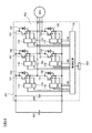
- FIG. 2 is a diagram illustrating a circuit configuration of the power conversion device 251.
- the power conversion device 251 includes an upper arm and a lower arm each including the IGBT 101 and the diode 102 corresponding to three phases including a U phase, a V phase, and a W phase of AC power. These three-phase upper and lower arms constitute an inverter circuit 902.
- the collector electrode of the upper arm IGBT 101 is electrically connected to the capacitor terminal on the positive side of the smoothing capacitor 255, and the emitter electrode of the lower arm IGBT 101 is electrically connected to the capacitor terminal on the negative side of the smoothing capacitor 255.
- the IGBT 101 includes a collector electrode, an emitter electrode, and a gate electrode.
- a diode 102 is electrically connected between the collector electrode and the emitter electrode.
- a MOSFET Metal Oxide Semiconductor Field Field Effect Transistor
- the diode 102 is unnecessary.
- IGBT is suitable when the DC voltage is relatively high, and MOSFET is suitable when the DC voltage is relatively low.
- the gate drive circuit 110 is provided between the emitter electrode of the IGBT 101 and the gate electrode, and controls the IGBT 101 on and off.
- the control circuit 150 supplies a control signal to the gate driving circuit 110.
- the IGBT 101 includes a current detection emitter electrode, and the output of the current detection emitter electrode is input to the overcurrent detection circuit 108.
- the overcurrent detection circuit 108 detects an overcurrent in which the main current flowing through the inverter circuit 902 having the upper and lower arms configured by the IGBT 101 exceeds a predetermined current
- the overcurrent detection circuit 108 notifies the control circuit 150 of this.
- the control circuit 150 causes a later-described saturation current circuit in the gate drive circuit 110 to function.
- the saturation current circuit limits the control current flowing to the gate electrode of the IGBT 101 to a predetermined saturation current.
- control circuit 150 receives a control command from the host control device, and generates a control signal for controlling the IGBT 101 that constitutes the upper arm or the lower arm of the inverter circuit 902 based on the control command. Supply. Based on the control signal, the gate drive circuit 110 supplies a drive signal for driving the IGBT 101 constituting the upper arm or the lower arm of each phase to the IGBT 101 of each phase.
- the IGBT 101 performs an on or off operation based on a drive signal from the gate drive circuit 110, converts the DC power supplied from the battery 901 into three-phase AC power, and the converted power is supplied to the motor generator MG. .
- FIG. 3 is a circuit diagram showing a main part of the power conversion device 251 according to the first embodiment of the present invention.
- the current detection emitter electrode and the overcurrent detection circuit 108 provided in the IGBT 101 are not shown.
- the IGBT 101 is ON / OFF controlled when the gate drive circuit 110 charges and discharges the gate capacitance 103.
- the collector wiring 104 and the auxiliary emitter wiring 105 of the IGBT 101 constitute a coupled inductor.
- the gate driving circuit 110 includes first to third switching elements 111, 112, and 113, a saturation current circuit 114, gate resistors 115 and 116, and a gate power source 117.
- the first switching element 111 is connected between the gate power supply 117 and the gate resistor 115, and is connected to the gate terminal of the IGBT 101 via the gate resistor 115.
- the gate capacitance 103 of the IGBT 101 is charged from the gate power supply 117 via the gate resistor 115.
- the IGBT 101 is controlled to be on.
- the second switching element 112 is connected between the ground potential 118 and the gate resistor 116, and is connected to the gate terminal of the IGBT 101 via the gate resistor 116.
- the gate capacitance 103 of the IGBT 101 is discharged through the gate resistance 116.
- the IGBT 101 is controlled to be off.
- the overcurrent detection circuit 108 see FIG. 2 does not detect that the main current flowing through the IGBT 101 is an overcurrent
- the first switching element 111 and the second switching element 112 perform on / off control of the IGBT 101.
- the saturation current circuit 114 is a circuit in which the gate and source of an N-channel JFET (Junction / Field / Effect / Transistor) are connected.
- the overcurrent detection circuit 108 detects that the main current flowing through the IGBT 101 is an overcurrent
- the third switching element 113 is turned on by a control signal from the control circuit 150 that receives a signal from the overcurrent detection circuit 108. To do. In this case, the control signal from the control circuit 150 is not input to the second switching element 112, and the second switching element 112 is off.
- the saturation current circuit 114 When the third switching element 113 is turned on, the gate capacitance 103 of the IGBT 101 is discharged through the saturation current circuit 114 at a slower rate than when the second switching element 112 is turned on. That is, the saturation current circuit 114 is provided in a control current path for turning off the IGBT 101, limits the control current to a predetermined saturation current, and turns off the IGBT 101. In other words, the saturation current circuit 114 suppresses the rate at which the gate voltage of the IGBT 101 decreases when turning off the IGBT 101.
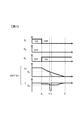
- FIG. 4 is a time chart of the gate drive circuit 110 and the IGBT 101 when an overcurrent is detected by the overcurrent detection circuit 108.
- Q 1 indicates the on / off timing of the first switching element 111
- Q 2 indicates the on / off timing of the second switching element 112
- Q 3 indicates the on / off timing of the third switching element 113.
- V GE indicates the gate voltage of the IGBT 101
- i G indicates the gate current of the IGBT 101.
- a solid line is a time chart in the power converter device 251 according to the present embodiment shown in FIG.
- a broken line is a comparative example, and shows a case where a resistance element is used instead of the saturation current circuit 114 of FIG. 3, for example.
- the overcurrent of the IGBT 101 refers to a current that exceeds the range of collector current that is normally used. When the overcurrent is detected and the IGBT 101 is turned off, the switching speed is slowed so that the surge voltage between the collector and the emitter of the IGBT 101 does not become excessive.
- causes of overcurrent include arm short circuit due to breakdown or malfunction of IGBT 101 or diode 102, output short circuit due to load breakdown, and the like.
- each switching element 111 to 113 and the change in gate voltage V GE and gate current i G will be described based on the passage of time (t 0 to t 2 , t 2 ′).
- the overcurrent of the IGBT 101 is detected by the overcurrent detection circuit 108, and the first switching element 111 (Q 1 ) is turned off by the control signal from the control circuit 150 that receives the signal from the overcurrent detection circuit 108.
- the third switching element 113 Q 3
- the second switching element 112 (Q 2 ) remains off.
- the gate capacitance 103 of the IGBT 101 is discharged through a path including the third switching element 113 (Q 3 ), and the gate voltage V GE of the IGBT 101 decreases with a time constant determined by the resistance in the current path of the gate capacitance 103 and the gate current i G. Beginning, the IGBT 101 remains on until the gate voltage V GE falls below the threshold voltage V TH of the IGBT 101.
- the gate voltage V GE of IGBT101 is lower than the threshold voltage V TH, the collector current of IGBT101 begins to decrease.
- the discharge current of the gate capacitance 103 of IGBT101 Coupled inductors by the collector wiring 104 and the auxiliary emitter wiring 105 is increased.
- the increase in the negative direction of the gate current i G increases from time t 1 to time t 2 when the gate voltage V GE of the IGBT 101 becomes 0.
- the gate voltage VGE decreases sharply.
- the rate of decrease in the collector current of the IGBT 101 becomes steep, and the surge voltage applied between the collector and the emitter of the IGBT 101 may become excessive.
- an increase in the discharge direction of the gate current i G between the time t 2 'of the gate voltage V GE from the time t 1 IGBT 101 becomes 0, the saturation current of the saturation current circuit 114 It is clamped by the value I SAT, to prevent a steep drop in the gate voltage V GE. Therefore, compared with the comparative example, the rate of decrease in the collector current of the IGBT 101 becomes moderate, and the surge voltage applied between the collector and the emitter of the IGBT 101 is suppressed.
- the saturation current circuit 114 suppresses the acceleration of the decrease in the gate voltage of the IGBT 101 due to the coupled inductor formed between the main current path flowing through the inverter circuit and the control current path.
- a surge voltage can be suppressed.
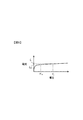
- FIG. 5 is a diagram illustrating the voltage-current characteristics of the saturation current circuit 114.
- the saturation current value ISAT is a current value at the threshold voltage VTH .
- a desirable characteristic for the saturation current circuit 114 is to provide a boundary between the linear region and the saturation region at a voltage value equal to or lower than the threshold voltage V TH , and as shown in FIG.
- the current value in the discharge direction is limited to the saturation current value I SAT to suppress a rapid drop in the gate voltage V GE .
- V b is a voltage value three times the threshold voltage V TH and I b is a current value at V b
- the saturation current is such that I b is 1.2 times or less of the saturation current value I SAT.
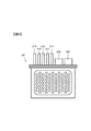
- FIG. 6 is a view showing the appearance of the power semiconductor module 201.
- a power semiconductor module 201 shown in FIG. 6 includes an IGBT 101 and a diode 102, and includes a collector terminal 202, an emitter terminal 203, a gate terminal 211, an auxiliary emitter terminal 212, a current detection terminal 213, and temperature detection terminals 214 and 215. ing.
- the collector terminal 202 and the auxiliary emitter terminal 212 are close to each other, so that a coupled inductor is formed without using a magnetic material. If the collector terminal 202 and the auxiliary emitter terminal 212 are brought closer to each other in order to reduce the size of the power converter 251, the coupling coefficient that is the degree of coupling of the coupled inductor increases, and the influence on the switching speed of the IGBT 101 increases. Therefore, in the power conversion device 251 according to the present embodiment, the surge voltage can be suppressed by the saturation current circuit 114 in the gate drive circuit 110 when the collector overcurrent of the IGBT 101 is cut off.
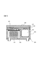
- FIG. 7 is a diagram showing a mounting structure of the power conversion device 251 using the power semiconductor module 201 of FIG.
- the power conversion device 251 includes housings 252, 253, 254, a power semiconductor module 201, a smoothing capacitor 255, a bus bar 256, a circuit board 257, and a flow path 258.
- the power semiconductor module 201 is cooled by the refrigerant flowing through the flow path 258.
- a gate drive circuit 110 and a control circuit 150 are mounted on the circuit board 257.
- the collector terminal 202 and the emitter terminal 203 of the power semiconductor module 201 are connected to the bus bar 256 by welding or soldering, and the gate terminal 211, the auxiliary emitter terminal 212, and the current detection terminal 213 of the power semiconductor module 201 are connected to the circuit board 257.
- the temperature detection terminals 214 and 215 are connected by soldering.
- FIG. 8 is a view showing an appearance of a power semiconductor module 501 incorporating power semiconductor elements for upper and lower arms.
- a power semiconductor module 501 shown in FIG. 8 includes a P terminal 502, an N terminal 503, an AC terminal 504, a gate terminal 511 of an upper arm power semiconductor element, an auxiliary emitter terminal 512, a current detection terminal 513, and a power semiconductor element of a lower arm.
- a gate terminal 521, an auxiliary emitter terminal 522, a current detection terminal 523, and temperature detection terminals 524 and 525 are provided.
- the P terminal 502 is a collector terminal of the upper arm
- the N terminal 503 is an emitter terminal of the lower arm
- the AC terminal 504 is a connection portion between the upper arm and the lower arm.
- the P inductor 502 and the auxiliary emitter terminal 512 are close to each other to form a coupled inductor.
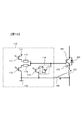
- FIG. 9 to 11 are circuit diagrams showing the main part of the power converter 251 having different coupled inductors.
- FIG. 3 shows the coupled inductor of the IGBT 101 collector and auxiliary emitter, other locations may constitute the coupled inductor.
- FIG. 9 is a circuit diagram showing a main part of the power converter 251 having a coupled inductor by the collector 104 and the gate 106 of the IGBT 101
- FIG. 10 shows the power converter 251 having a coupled inductor by the emitter 107 and the auxiliary emitter 105 of the IGBT 101
- FIG. 11 is a circuit diagram showing a main part of a power conversion device 251 having a coupled inductor formed by the emitter 107 and the gate 106 of the IGBT 101.
- the saturation current circuit 114 in the gate drive circuit 110 can suppress the surge voltage between the collector and the emitter of the IGBT 101.
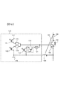
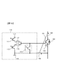
- FIG. 12 and 13 are circuit diagrams showing the main part of the power converter 251.
- a resistance element or a capacitance element may be added to the saturation current circuit 114.
- FIG. 12 shows an example in which a resistance element 121 is connected in series to the JFET of the saturation current circuit 114.
- FIG. 13 shows an example in which the capacitive element 122 is connected in parallel to the series circuit of the third switching element 113 and the saturation current circuit 114.
- the substantial gate capacitance can be increased. 12 and 13, the surge current between the collector and emitter of the IGBT 101 can be suppressed by the saturation current circuit 114 in the gate drive circuit 110.
- FIG. 14 is a graph showing a surge voltage between the collector and the emitter of the IGBT 101.
- the vertical axis represents the collector-emitter voltage
- the horizontal axis represents time.
- the graph shown by the solid line in FIG. 14 is a simulation waveform when the overcurrent of the IGBT 101 is cut off in the power conversion device 251 according to this embodiment using the saturation current circuit 114 shown in FIG.
- a graph indicated by a broken line in FIG. 14 shows a simulation waveform in the case of a comparative example using a resistance element instead of the saturation current circuit 114 shown in FIG.
- the peak value of the surge voltage in this embodiment is reduced by 230 V compared to the peak value of the surge voltage when the saturation current circuit 114 is not used. Moreover, the Joule loss generated when the overcurrent was cut off was the same in both cases. Thus, according to the present embodiment, the surge voltage between the collector and the emitter of the IGBT 101 can be reduced.
- FIG. 15 is a circuit diagram illustrating a main part of the power conversion device 251 according to the second embodiment.
- the current detection emitter electrode and the overcurrent detection circuit 108 provided in the IGBT 101 are not shown.
- an nMOSFET metal-oxide-semiconductor junction field effect transistor
- the saturation current circuit 3114 is ON at the time of Q 3 shown in FIG.
- the nMOSFET as the saturation current circuit 314 is turned on with a lower gate voltage than when the second switching element 112 is turned on.
- the power conversion apparatus 251 similarly to the time chart shown in FIG. 4, during the time t 2 'of the gate voltage V GE from the time t 1 IGBT 101 becomes zero discharge direction of the gate current i G The increase is clamped by the saturation current value I SAT of the saturation current circuit 314 to prevent a sharp decrease in the gate voltage V GE . For this reason, the rate of decrease in the collector current of the IGBT 101 becomes moderate, and the surge voltage applied between the collector and the emitter of the IGBT 101 can be suppressed.
- the switching speed of the IGBT 101 can be suppressed, the surge voltage can be suppressed.
- the third switching element 113 shown in FIG. 3 can be deleted.
- the nMOSFET can obtain the same voltage-current characteristics as shown in FIG.
- the number of components of the power conversion device 251 can be reduced.
- FIG. 16 is a circuit diagram illustrating a main part of a power converter 251 according to the third embodiment.
- the current detection emitter electrode and the overcurrent detection circuit 108 provided in the IGBT 101 are not shown.
- an N-channel JFET is used as the saturation current circuit 414.
- the JFET junction field effect transistor
- the saturation current circuit 414 is ON at the time of Q 3 shown in FIG.
- a negative voltage is applied to the gate, and when turning on the JFET, a zero (GND) voltage is applied to the gate.
- the power conversion apparatus 251 similarly to the time chart shown in FIG. 4, during the time t 2 'of the gate voltage V GE from the time t 1 IGBT 101 becomes zero discharge direction of the gate current i G The increase is clamped by the saturation current value I SAT of the saturation current circuit 414 to prevent a sharp decrease in the gate voltage V GE . For this reason, the rate of decrease in the collector current of the IGBT 101 becomes moderate, and the surge voltage applied between the collector and the emitter of the IGBT 101 can be suppressed.
- the switching speed of the IGBT 101 can be suppressed, the surge voltage can be suppressed. Furthermore, in the present embodiment, the third switching element 113 shown in FIG. 3 can be deleted. According to the present embodiment, in addition to the same effects as those of the first embodiment, the number of components of the power conversion device 251 can be reduced.
- the power conversion device 251 is provided in the path of the IGBT 101 that is on / off controlled by the gate drive circuit 110 and the control current that turns off the IGBT 101, and the saturation that limits the control current to a predetermined saturation current and turns off the IGBT 101. And a current circuit 114. Thereby, the surge voltage of power semiconductor elements, such as IGBT101, can be reduced.
- the present invention can be implemented by modifying the first to third embodiments described above as follows.
- normal ON / OFF control of the IGBT 101 is performed by a series circuit of the third switching element 113 and the saturation current circuit 114. Further, when an overcurrent is detected in the IGBT 101, the IGBT 101 is controlled to be OFF.
- the saturation current circuits 314 and 414 are provided in parallel with the second switching element 112, but the second switching element 112 may be omitted. In this case, normal ON / OFF control of the IGBT 101 is performed by the saturation current circuits 314 and 414. Further, when an overcurrent is detected in the IGBT 101, the IGBT 101 is controlled to be OFF.
- the present invention is not limited to the above-described embodiment, and other forms conceivable within the scope of the technical idea of the present invention are also included in the scope of the present invention as long as the characteristics of the present invention are not impaired. . Moreover, it is good also as a structure which combined the above-mentioned embodiment and a some modification.
Landscapes
- Engineering & Computer Science (AREA)
- Power Engineering (AREA)
- Power Conversion In General (AREA)
- Inverter Devices (AREA)
- Electronic Switches (AREA)
Abstract
大きな主電流を遮断するときに、パワー半導体素子の主端子に過度なサージ電圧が発生する虞がある。 第3スイッチング素子113は、過電流検出回路108によりIGBT101に流れる主電流が過電流であることが検知され、過電流検出回路108からの信号を受けた制御回路150からの制御信号によりオンする。なお、この場合、第2スイッチング素子112には、制御回路150からの制御信号は入力されず、第2スイッチング素子112はオフしている。第3スイッチング素子113がオンしたときに、飽和電流回路114を介してIGBT101のゲート容量103は第2スイッチング素子112がオンする場合よりも遅い速度で放電される。
Description
本発明は、電力変換装置に関する。
ハイブリッド自動車や電気自動車では、モータを駆動するために電力変換装置が用いられている。電力変換装置は、IGBT(Insulated Gate Bipolar Transistor)、MOSFET(Metal Oxide Semiconductor Field Effect Transistor)などのパワー半導体素子を用いたインバータ回路により構成される。そして電力変換装置は、小型化や低損失化、高信頼化が求められる。
特許文献1には、パワー半導体素子の主電流が流れる経路の周囲にインダクタを配置し、そのインダクタをパワー半導体素子のゲートに接続することでパワー半導体素子の高速動作を可能にする回路が開示されている。
上述した、特許文献1に記載の回路では、大きな主電流を遮断するときに、主電流経路と制御電流経路との間に形成される結合インダクタによってパワー半導体素子のゲート電圧の低下する速度が速くなり、パワー半導体素子に過度なサージ電圧が発生する虞がある。
本発明による電力変換装置は、ゲート駆動回路によりオンオフ制御されるパワー半導体素子と、前記パワー半導体素子をオフする制御電流の経路内に設けられ、前記制御電流を所定の飽和電流に制限して前記パワー半導体素子をオフする飽和電流回路とを備えた。
本発明によれば、パワー半導体素子のサージ電圧を低減できる。
(第1の実施形態)
本実施形態に係る電力変換装置について、図面を参照しながら説明する。本実施形態に係る電力変換装置は、ハイブリッド用の自動車や電気自動車に適用可能であるが、一例として、ハイブリッド自動車に適用した場合について説明する。
本実施形態に係る電力変換装置について、図面を参照しながら説明する。本実施形態に係る電力変換装置は、ハイブリッド用の自動車や電気自動車に適用可能であるが、一例として、ハイブリッド自動車に適用した場合について説明する。
図1はハイブリッド方式の自動車のシステム構成を示す図である。内燃機関EGNおよびモータジェネレータMGは自動車の走行用トルクを発生する動力源である。また、モータジェネレータMGは回転トルクを発生するだけでなく、モータジェネレータMGに加えられる機械エネルギ(回転力)を電力に変換する機能を有する。モータジェネレータMGは、例えば同期電動/発電機あるいは誘導電動/発電機であり、自動車の運転方法により電動機としても発電機としても動作する。
内燃機関EGNの出力側は動力分配機構TSMを介してモータジェネレータMGに伝達され、動力分配機構TSMからの回転トルクあるいはモータジェネレータMGが発生する回転トルクは、トランスミッションTMおよびデファレンシャルギアDEFを介して車輪WHに伝達される。
一方、回生制動の運転時には、車輪WHから回転トルクがモータジェネレータMGに伝達され、伝達された回転トルクに基づいてモータジェネレータMGは交流電力を発生する。発生した交流電力は電力変換装置251により直流電力に変換され、高電圧用のバッテリ901を充電し、充電された電力は再び走行エネルギとして使用される。
電力変換装置251は、インバータ回路902、平滑コンデンサ255を備える。インバータ回路902は平滑コンデンサ255を介してバッテリ901と電気的に接続されており、バッテリ901とインバータ回路902との相互において電力の授受が行われる。平滑コンデンサ255は、インバータ回路902に供給される直流電力を平滑化する。
電力変換装置251の制御回路150は、通信用のコネクタ903を介して上位の制御装置から指令を受けたり、上位の制御装置に状態を表すデータを送信する。制御回路150は、入力される指令に基づいて、モータジェネレータMGの制御量を演算し、演算結果に基づいて制御信号を発生してゲート駆動回路110へ制御信号を供給する。この制御信号に基づいてゲート駆動回路110がインバータ回路902を制御するための駆動信号を発生する。
モータジェネレータMGを電動機として動作させる場合には、インバータ回路902はバッテリ901から供給された直流電力に基づき交流電力を発生し、モータジェネレータMGに供給する。モータジェネレータMGとインバータ回路902からなる構成は電動/発電ユニットとして動作する。
図2は、電力変換装置251の回路構成を示す図である。以下の説明ではパワー半導体素子としてIGBT(Insulated Gate Bipolar Transistor)を使用した例で説明する。
電力変換装置251は、IGBT101及びダイオード102を備えてなる上アームおよび下アームを、交流電力のU相、V相、W相からなる3相に対応して備えている。これらの3相の上下アームはインバータ回路902を構成する。
電力変換装置251は、IGBT101及びダイオード102を備えてなる上アームおよび下アームを、交流電力のU相、V相、W相からなる3相に対応して備えている。これらの3相の上下アームはインバータ回路902を構成する。
上アームのIGBT101のコレクタ電極は平滑コンデンサ255の正極側のコンデンサ端子に、下アームのIGBT101のエミッタ電極は平滑コンデンサ255の負極側のコンデンサ端子にそれぞれ電気的に接続されている。
IGBT101はコレクタ電極、エミッタ電極、ゲート電極を備えている。また、ダイオード102がコレクタ電極とエミッタ電極との間に電気的に接続されている。なお、パワー半導体素子として、MOSFET(Metal Oxide Semiconductor Field Effect Transistor)を用いてもよく、この場合、ダイオード102は不要である。パワー半導体素子としてIGBTは直流電圧が比較的高い場合に適していて、MOSFETは直流電圧が比較的低い場合に適している。
ゲート駆動回路110は、IGBT101のエミッタ電極と、ゲート電極との間に設けられ、IGBT101をオンオフ制御する。制御回路150は、ゲート駆動回路110へ制御信号を供給する。
IGBT101は、電流検出用エミッタ電極を備え、電流検出用エミッタ電極の出力は過電流検出回路108へ入力される。過電流検出回路108は、IGBT101により上下アームが構成されたインバータ回路902に流れる主電流が所定電流以上となる過電流を検知すると、これを制御回路150へ通知する。制御回路150は、この通知を受けて、ゲート駆動回路110内の後述する飽和電流回路を機能させる。飽和電流回路は、IGBT101のゲート電極へ流れる制御電流を所定の飽和電流に制限する。なお、IGBT101に流れる過電流を検出する方法は種々の方法があり、本実施形態に限定しない。
上述のように、制御回路150は上位の制御装置から制御指令を受け、これに基づいてインバータ回路902の上アームあるいは下アームを構成するIGBT101を制御する制御信号を発生し、ゲート駆動回路110に供給する。ゲート駆動回路110は制御信号に基づき各相の上アームあるいは下アームを構成するIGBT101を駆動するための駆動信号を各相のIGBT101に供給する。
IGBT101はゲート駆動回路110からの駆動信号に基づき、オンあるいはオフ動作を行い、バッテリ901から供給された直流電力を三相交流電力に変換し、この変換された電力はモータジェネレータMGに供給される。
(第1の実施形態)
図3は、本発明の第1の実施形態に係る電力変換装置251の要部を示す回路図である。なお、IGBT101に備えられている電流検出用エミッタ電極および過電流検出回路108は図示を省略する。
図3は、本発明の第1の実施形態に係る電力変換装置251の要部を示す回路図である。なお、IGBT101に備えられている電流検出用エミッタ電極および過電流検出回路108は図示を省略する。
IGBT101はゲート駆動回路110がゲート容量103を充放電することでオン、オフ制御される。IGBT101のコレクタ配線104と補助エミッタ配線105は結合インダクタを構成する。ゲート駆動回路110は、第1~第3スイッチング素子111、112、113および飽和電流回路114、ゲート抵抗115、116、ゲート電源117で構成される。
第1スイッチング素子111は、ゲート電源117とゲート抵抗115の間に接続され、ゲート抵抗115を介してIGBT101のゲート端子に接続される。そして、制御回路150からの制御信号により第1スイッチング素子111がオンしたときに、IGBT101のゲート容量103はゲート抵抗115を介してゲート電源117より充電される。その結果、IGBT101はオンに制御される。
第2スイッチング素子112は、グランド電位118とゲート抵抗116の間に接続され、ゲート抵抗116を介してIGBT101のゲート端子に接続される。そして、制御回路150からの制御信号により第2スイッチング素子112がオンしたときに、IGBT101のゲート容量103はゲート抵抗116を介して放電される。その結果、IGBT101はオフに制御される。過電流検出回路108(図2参照)によりIGBT101に流れる主電流が過電流であることが検出されない通常の状態では、第1スイッチング素子111および第2スイッチング素子112により、IGBT101はオンオフ制御される。
第3スイッチング素子113は、一方がグランド電位118に接続され、他方が飽和電流回路114を介してIGBT101のゲート端子に接続されている。飽和電流回路114は、NチャンネルJFET(Junction Field Effect Transistor)のゲートとソースを接続した回路である。第3スイッチング素子113は、過電流検出回路108によりIGBT101に流れる主電流が過電流であることが検知されると、過電流検出回路108からの信号を受けた制御回路150からの制御信号によりオンする。なお、この場合、第2スイッチング素子112には、制御回路150からの制御信号は入力されず、第2スイッチング素子112はオフしている。第3スイッチング素子113がオンしたときに、飽和電流回路114を介してIGBT101のゲート容量103は第2スイッチング素子112がオンする場合よりも遅い速度で放電される。すなわち、飽和電流回路114は、IGBT101をオフする制御電流の経路内に設けられ、制御電流を所定の飽和電流に制限してIGBT101をオフする。換言すれば、飽和電流回路114は、IGBT101をオフするときに、IGBT101のゲート電圧が低下する速度を抑制する。
図4は、過電流検出回路108で過電流が検知された場合のゲート駆動回路110とIGBT101のタイムチャートである。
図4において、Q1は第1スイッチング素子111のオン、オフのタイミングを示し、Q2は第2スイッチング素子112のオンオフのタイミングを示し、Q3は第3スイッチング素子113のオン、オフのタイミングを示す。更に、VGEはIGBT101のゲート電圧を示し、iGはIGBT101のゲート電流を示している。図4において、実線が図3に示す本実施形態に係る電力変換装置251におけるタイムチャートである。図4において、破線は比較例であり、例えば図3の飽和電流回路114の代わりに抵抗素子を用いた場合を示している。
図4において、Q1は第1スイッチング素子111のオン、オフのタイミングを示し、Q2は第2スイッチング素子112のオンオフのタイミングを示し、Q3は第3スイッチング素子113のオン、オフのタイミングを示す。更に、VGEはIGBT101のゲート電圧を示し、iGはIGBT101のゲート電流を示している。図4において、実線が図3に示す本実施形態に係る電力変換装置251におけるタイムチャートである。図4において、破線は比較例であり、例えば図3の飽和電流回路114の代わりに抵抗素子を用いた場合を示している。
IGBT101の過電流とは、通常使用するコレクタ電流の範囲を超過した電流を言う。そして、過電流を検知してIGBT101をオフしたときに、IGBT101のコレクタ-エミッタ間のサージ電圧が過大にならないようスイッチング速度を遅くする。過電流の原因には、IGBT101やダイオード102の破壊または誤動作によるアーム短絡や負荷の破壊による出力短絡等がある。
図4を参照して、各スイッチング素子111~113の動作およびゲート電圧VGE、ゲート電流iGの変化を、時刻(t0~t2、t2’)の経過に基づいて説明する。
時刻t0では、IGBT101の過電流を過電流検出回路108により検知し、過電流検出回路108からの信号を受けた制御回路150からの制御信号により、第1スイッチング素子111(Q1)がオフし、第3スイッチング素子113(Q3)がオンする。第2スイッチング素子112(Q2)はオフのままである。IGBT101のゲート容量103は第3スイッチング素子113(Q3)を含む経路で放電され、IGBT101のゲート電圧VGEはゲート容量103とゲート電流iGの電流経路内の抵抗で決まる時定数で下降を始めるが、ゲート電圧VGEがIGBT101のしきい値電圧VTHを下回るまでは、IGBT101はオンしたままである。
時刻t0では、IGBT101の過電流を過電流検出回路108により検知し、過電流検出回路108からの信号を受けた制御回路150からの制御信号により、第1スイッチング素子111(Q1)がオフし、第3スイッチング素子113(Q3)がオンする。第2スイッチング素子112(Q2)はオフのままである。IGBT101のゲート容量103は第3スイッチング素子113(Q3)を含む経路で放電され、IGBT101のゲート電圧VGEはゲート容量103とゲート電流iGの電流経路内の抵抗で決まる時定数で下降を始めるが、ゲート電圧VGEがIGBT101のしきい値電圧VTHを下回るまでは、IGBT101はオンしたままである。
時刻t1では、IGBT101のゲート電圧VGEはしきい値電圧VTHを下回り、IGBT101のコレクタ電流は減少し始める。IGBT101のコレクタ電流の減少の速度に応じて、コレクタ配線104と補助エミッタ配線105による結合インダクタによりIGBT101のゲート容量103の放電電流(ゲート電流iGの負方向)が増加する。
比較例の電力変換装置では、図4の破線で示すように、時刻t1からIGBT101のゲート電圧VGEが0になる時刻t2の間においてゲート電流iGの負方向への増加が大きくなり、ゲート電圧VGEの低下が急峻になる。そのため、IGBT101のコレクタ電流の減少の速度が急峻になり、IGBT101のコレクタ-エミッタ間に印加されるサージ電圧が過大になる虞がある。
本実施形態に係る電力変換装置251では、時刻t1からIGBT101のゲート電圧VGEが0になる時刻t2’の間においてゲート電流iGの放電方向の増加は、飽和電流回路114の飽和電流値ISATでクランプされ、ゲート電圧VGEの急峻な低下を防止する。そのため、比較例と比べて、IGBT101のコレクタ電流の減少の速度が緩やかになり、IGBT101のコレクタ-エミッタ間に印加されるサージ電圧を抑制する。すなわち、飽和電流回路114は、IGBT101をオフするときに、インバータ回路に流れる主電流の経路と制御電流の経路の間に形成された結合インダクタによるIGBT101のゲート電圧の低下の加速を抑制する。このように、本実施形態によれば、IGBT101のスイッチング速度を抑えることができるため、サージ電圧を抑制できる。
図5は、飽和電流回路114の電圧電流特性を示す図である。飽和電流値ISATはしきい値電圧VTHにおける電流値である。飽和電流回路114として望ましい特性は、しきい値電圧VTH以下の電圧値に線形領域と飽和領域との境界を設けることで、図4に示したように、IGBT101の過電流遮断時のゲート電流の放電方向の電流値を飽和電流値ISATに制限し、ゲート電圧VGEの急激な低下を抑える。さらに、Vbをしきい値電圧VTHの3倍の電圧値、IbをVbにおける電流値としたとき、Ibが飽和電流値ISATの1.2倍以下になるような飽和電流回路114を用いることで、効果的にサージ電圧を抑制する。
図6は、パワー半導体モジュール201の外観を示す図である。図6に示すパワー半導体モジュール201は、IGBT101、ダイオード102を内蔵しており、コレクタ端子202、エミッタ端子203、ゲート端子211、補助エミッタ端子212、電流検出端子213、温度検出端子214、215を備えている。
図6において、コレクタ端子202と補助エミッタ端子212とが近接することで、磁性体を用いなくても結合インダクタが形成される。電力変換装置251を小型化するために、コレクタ端子202と補助エミッタ端子212をより近接させると結合インダクタの結合の度合いである結合係数は増加し、IGBT101のスイッチング速度に与える影響は大きくなる。そこで、本実施形態に係る電力変換装置251ではIGBT101のコレクタ過電流遮断時には、ゲート駆動回路110内の飽和電流回路114によって、サージ電圧を抑制できる。
図7は、図6のパワー半導体モジュール201を用いた電力変換装置251の実装構造を示す図である。電力変換装置251は、筺体252、253、254、パワー半導体モジュール201、平滑コンデンサ255、バスバー256、回路基板257、流路258を備えている。パワー半導体モジュール201は、流路258を流れる冷媒によって冷却される。回路基板257には、ゲート駆動回路110や制御回路150が搭載される。バスバー256には、パワー半導体モジュール201のコレクタ端子202、エミッタ端子203が溶接または半田付けで接続され、回路基板257には、パワー半導体モジュール201のゲート端子211、補助エミッタ端子212、電流検出端子213、温度検出端子214、215が半田付けで接続される。
図8は、上下アーム分のパワー半導体素子を内蔵したパワー半導体モジュール501の外観を示す図である。図8に示すパワー半導体モジュール501は、P端子502、N端子503、AC端子504、上アームのパワー半導体素子のゲート端子511、補助エミッタ端子512、電流検出端子513、下アームのパワー半導体素子のゲート端子521、補助エミッタ端子522、電流検出端子523、温度検出端子524、525を備えている。なお、P端子502は上アームのコレクタ端子、N端子503は下アームのエミッタ端子、AC端子504は上アームと下アームの接続部である。図8において、P端子502と補助エミッタ端子512とが近接することで、結合インダクタが形成される。
図9~図11は、それぞれ結合インダクタが異なる電力変換装置251の要部を示す回路図である。図3では、IGBT101のコレクタと補助エミッタの結合インダクタを示したが、他の箇所が結合インダクタを構成してもよい。
図9は、IGBT101のコレクタ104とゲート106による結合インダクタを持つ電力変換装置251の要部を示す回路図、図10は、IGBT101のエミッタ107と補助エミッタ105による結合インダクタを持つ電力変換装置251の要部を示す回路図、図11は、IGBT101のエミッタ107とゲート106による結合インダクタを持つ電力変換装置251の要部を示す回路図である。図9~図11のいずれの場合も、ゲート駆動回路110内の飽和電流回路114によって、IGBT101のコレクタ-エミッタ間のサージ電圧を抑制できる。
図12、13は、電力変換装置251の要部を示す回路図である。これらの図に示すように、飽和電流回路114に抵抗素子や容量素子を追加してもよい。
図12は、飽和電流回路114のJFETに直列に抵抗素子121を接続した例を示す。図13は、第3スイッチング素子113と飽和電流回路114の直列回路に対して並列に容量素子122を接続した例を示す。図13に示す回路図では実質的なゲート容量を大きくすることができる。図12、13のいずれの場合も、ゲート駆動回路110内の飽和電流回路114によって、IGBT101のコレクタ-エミッタ間のサージ電圧を抑制できる。
図12は、飽和電流回路114のJFETに直列に抵抗素子121を接続した例を示す。図13は、第3スイッチング素子113と飽和電流回路114の直列回路に対して並列に容量素子122を接続した例を示す。図13に示す回路図では実質的なゲート容量を大きくすることができる。図12、13のいずれの場合も、ゲート駆動回路110内の飽和電流回路114によって、IGBT101のコレクタ-エミッタ間のサージ電圧を抑制できる。
図14は、IGBT101のコレクタ-エミッタ間のサージ電圧を示すグラフである。図14の縦軸はコレクタ-エミッタ間の電圧、横軸は時間である。
図14の実線で示すグラフは、図3に示す飽和電流回路114を用いた本実施形態に係る電力変換装置251において、IGBT101の過電流を遮断した場合のシミュレーション波形である。一方、図14の破線で示すグラフは、図3に示す飽和電流回路114の代わりに抵抗素子を用いた比較例の場合のシミュレーション波形を示している。
図14の実線で示すグラフは、図3に示す飽和電流回路114を用いた本実施形態に係る電力変換装置251において、IGBT101の過電流を遮断した場合のシミュレーション波形である。一方、図14の破線で示すグラフは、図3に示す飽和電流回路114の代わりに抵抗素子を用いた比較例の場合のシミュレーション波形を示している。
図14より、本実施形態におけるサージ電圧のピーク値は、飽和電流回路114を用いない場合のサージ電圧のピーク値と比較して、230V低減された。また、過電流を遮断した時に生じるジュール損失は両者で同等であった。このように、本実施形態によれば、IGBT101のコレクタ-エミッタ間のサージ電圧を低減できる。
(第2の実施形態)
図15は、第2の実施形態に係る電力変換装置251の要部を示す回路図である。なお、IGBT101に備えられている電流検出用エミッタ電極および過電流検出回路108は図示を省略する。
本実施形態においては、飽和電流回路314としてnMOSFET(金属-酸化物-半導体接合電界効果トランジスタ)を用いる。過電流が検出された場合に、飽和電流回路314としてのnMOSFETを、図4に示すQ3のタイミングでオンする。さらに、第2スイッチング素子112がオンするときよりも低いゲート電圧で飽和電流回路314としてのnMOSFETをオンさせる。
図15は、第2の実施形態に係る電力変換装置251の要部を示す回路図である。なお、IGBT101に備えられている電流検出用エミッタ電極および過電流検出回路108は図示を省略する。
本実施形態においては、飽和電流回路314としてnMOSFET(金属-酸化物-半導体接合電界効果トランジスタ)を用いる。過電流が検出された場合に、飽和電流回路314としてのnMOSFETを、図4に示すQ3のタイミングでオンする。さらに、第2スイッチング素子112がオンするときよりも低いゲート電圧で飽和電流回路314としてのnMOSFETをオンさせる。
本実施形態に係る電力変換装置251では、図4に示すタイムチャートと同様に、時刻t1からIGBT101のゲート電圧VGEが0になる時刻t2’の間においてゲート電流iGの放電方向の増加は、飽和電流回路314の飽和電流値ISATでクランプされ、ゲート電圧VGEの急峻な低下を防止する。そのため、IGBT101のコレクタ電流の減少の速度が緩やかになり、IGBT101のコレクタ-エミッタ間に印加されるサージ電圧を抑制できる。
このように、本実施形態によれば、IGBT101のスイッチング速度を抑えることができるため、サージ電圧を抑制できる。さらに、本実施形態では、図3に示す第3スイッチング素子113を削除することができる。これにより、nMOSFETは、図5に示したのと同様の電圧電流特性を得られる。本実施形態によれば、第1の実施形態と同様の効果に加えて、電力変換装置251の部品数を削減できる。
(第3の実施形態)
図16は、第3の実施形態に係る電力変換装置251の要部を示す回路図である。なお、IGBT101に備えられている電流検出用エミッタ電極および過電流検出回路108は図示を省略する。
本実施形態においては、飽和電流回路414としてNチャンネルJFETを用いる。過電流が検出された場合に、飽和電流回路414としてのJFET(接合型電界効果トランジスタ)を、図4に示すQ3のタイミングでオンする。なお、JFETをオフする場合はゲートに負の電圧を印加し、JFETをオンする場合はゲートにゼロ(GND)の電圧を印加する。
図16は、第3の実施形態に係る電力変換装置251の要部を示す回路図である。なお、IGBT101に備えられている電流検出用エミッタ電極および過電流検出回路108は図示を省略する。
本実施形態においては、飽和電流回路414としてNチャンネルJFETを用いる。過電流が検出された場合に、飽和電流回路414としてのJFET(接合型電界効果トランジスタ)を、図4に示すQ3のタイミングでオンする。なお、JFETをオフする場合はゲートに負の電圧を印加し、JFETをオンする場合はゲートにゼロ(GND)の電圧を印加する。
本実施形態に係る電力変換装置251では、図4に示すタイムチャートと同様に、時刻t1からIGBT101のゲート電圧VGEが0になる時刻t2’の間においてゲート電流iGの放電方向の増加は、飽和電流回路414の飽和電流値ISATでクランプされ、ゲート電圧VGEの急峻な低下を防止する。そのため、IGBT101のコレクタ電流の減少の速度が緩やかになり、IGBT101のコレクタ-エミッタ間に印加されるサージ電圧を抑制できる。
このように、本実施形態によれば、IGBT101のスイッチング速度を抑えることができるため、サージ電圧を抑制できる。さらに、本実施形態では、図3に示す第3スイッチング素子113を削除することができる。本実施形態によれば、第1の実施形態と同様の効果に加えて、電力変換装置251の部品数を削減できる。
以上説明した実施形態によれば、次の作用効果が得られる。
(1)電力変換装置251は、ゲート駆動回路110によりオンオフ制御されるIGBT101と、IGBT101をオフする制御電流の経路内に設けられ、制御電流を所定の飽和電流に制限してIGBT101をオフする飽和電流回路114とを備える。これにより、IGBT101などのパワー半導体素子のサージ電圧を低減できる。
(1)電力変換装置251は、ゲート駆動回路110によりオンオフ制御されるIGBT101と、IGBT101をオフする制御電流の経路内に設けられ、制御電流を所定の飽和電流に制限してIGBT101をオフする飽和電流回路114とを備える。これにより、IGBT101などのパワー半導体素子のサージ電圧を低減できる。
(変形例)
本発明は、以上説明した第1~第3の実施形態を次のように変形して実施することができる。
(1)第1の実施形態では、第2スイッチング素子112と並列に、第3スイッチング素子113と飽和電流回路114との直列回路を設けたが、第2スイッチング素子112を省略してもよい。この場合、第3スイッチング素子113と飽和電流回路114との直列回路で、IGBT101の通常のオンオフ制御を行い、さらに、IGBT101に過電流が検知された場合は、IGBT101のオフ制御を行う。
本発明は、以上説明した第1~第3の実施形態を次のように変形して実施することができる。
(1)第1の実施形態では、第2スイッチング素子112と並列に、第3スイッチング素子113と飽和電流回路114との直列回路を設けたが、第2スイッチング素子112を省略してもよい。この場合、第3スイッチング素子113と飽和電流回路114との直列回路で、IGBT101の通常のオンオフ制御を行い、さらに、IGBT101に過電流が検知された場合は、IGBT101のオフ制御を行う。
(2)第2~第3実施形態では、第2スイッチング素子112と並列に、飽和電流回路314、414を設けたが、第2スイッチング素子112を省略してもよい。この場合、飽和電流回路314、414で、IGBT101の通常のオンオフ制御を行い、さらに、IGBT101に過電流が検知された場合は、IGBT101のオフ制御を行う。
本発明は、上記の実施形態に限定されるものではなく、本発明の特徴を損なわない限り、本発明の技術思想の範囲内で考えられるその他の形態についても、本発明の範囲内に含まれる。また、上述の実施形態と複数の変形例を組み合わせた構成としてもよい。
101 IGBT
102 ダイオード
103 ゲート容量
104、105、106、107 結合インダクタ
110 ゲート駆動回路
111 第1スイッチング素子
112 第2スイッチング素子
113 第3スイッチング素子
114、314、414 飽和電流回路
115、116 ゲート抵抗
117 ゲート電源
118 グランド電位
122 容量素子
150 マイコン回路
201、501 パワー半導体モジュール
202 コレクタ端子
203 エミッタ端子
211、511、521 ゲート端子
212、512、522 補助エミッタ端子
213、513、523 電流検出端子
214、215、524、525 温度検出端子
251 電力変換装置
252、253、254 筺体
255 平滑コンデンサ
256 バスバー
257 回路基板
258 流路
502 P端子
503 N端子
504 AC端子
901 バッテリ
902 インバータ回路
903 コネクタ
Claims (7)
- ゲート駆動回路によりオンオフ制御されるパワー半導体素子と、
前記パワー半導体素子をオフする制御電流の経路内に設けられ、前記制御電流を所定の飽和電流に制限して前記パワー半導体素子をオフする飽和電流回路と
を備えた電力変換装置。 - 請求項1に記載の電力変換装置において、
前記飽和電流回路は、前記パワー半導体素子をオフするときに、前記パワー半導体素子のゲート電圧が低下する速度を抑制する電力変換装置。 - 請求項1に記載の電力変換装置において、
前記パワー半導体素子により上下アームが構成されたインバータ回路を備え、
前記飽和電流回路は、前記パワー半導体素子をオフするときに、前記インバータ回路に流れる主電流の経路と前記制御電流の経路の間に形成された結合インダクタによる前記パワー半導体素子のゲート電圧の低下の加速を抑制する電力変換装置。 - 請求項1から請求項3までのいずれか一項に記載の電力変換装置において、
前記飽和電流回路は、前記パワー半導体素子のしきい値電圧と前記しきい値電圧の3倍電圧との間の電圧領域において、導通電流の変化が1.2倍以下となる電圧電流特性を有する電力変換装置。 - 請求項1から請求項3までのいずれか一項に記載の電力変換装置において、
前記飽和電流回路は、前記制御電流を前記飽和電流に制限する接合型電界効果トランジスタによって構成される電力変換装置。 - 請求項1または請求項2に記載の電力変換装置において、
前記パワー半導体素子により上下アームが構成されたインバータ回路と、
前記インバータ回路に流れる主電流が所定電流以上となる過電流を検知する過電流検知回路と、を備え、
前記飽和電流回路は、前記過電流検知回路で前記過電流を検知した場合に、前記制御電流を前記飽和電流に制限する電力変換装置。 - 請求項6に記載の電力変換装置において、
前記過電流検知回路で前記過電流を検知した場合に、前記パワー半導体素子をオフする前記飽和電流回路の駆動電圧は、前記ゲート駆動回路の駆動電圧よりも低い電力変換装置。
Applications Claiming Priority (2)
| Application Number | Priority Date | Filing Date | Title |
|---|---|---|---|
| JP2016-164802 | 2016-08-25 | ||
| JP2016164802A JP2018033259A (ja) | 2016-08-25 | 2016-08-25 | 電力変換装置 |
Publications (1)
| Publication Number | Publication Date |
|---|---|
| WO2018037720A1 true WO2018037720A1 (ja) | 2018-03-01 |
Family
ID=61246593
Family Applications (1)
| Application Number | Title | Priority Date | Filing Date |
|---|---|---|---|
| PCT/JP2017/024427 Ceased WO2018037720A1 (ja) | 2016-08-25 | 2017-07-04 | 電力変換装置 |
Country Status (2)
| Country | Link |
|---|---|
| JP (1) | JP2018033259A (ja) |
| WO (1) | WO2018037720A1 (ja) |
Cited By (1)
| Publication number | Priority date | Publication date | Assignee | Title |
|---|---|---|---|---|
| CN116345863A (zh) * | 2021-12-23 | 2023-06-27 | 圣邦微电子(北京)股份有限公司 | 一种电压转换器中保持上管截止的泄放电路及方法 |
Families Citing this family (3)
| Publication number | Priority date | Publication date | Assignee | Title |
|---|---|---|---|---|
| JP7310563B2 (ja) | 2019-11-18 | 2023-07-19 | 富士電機株式会社 | 電圧制御型電力用半導体素子の駆動回路 |
| JP7413980B2 (ja) * | 2020-11-10 | 2024-01-16 | 株式会社豊田自動織機 | 電力変換装置 |
| WO2026074624A1 (ja) * | 2024-10-02 | 2026-04-09 | 日産自動車株式会社 | 電力変換装置 |
Citations (3)
| Publication number | Priority date | Publication date | Assignee | Title |
|---|---|---|---|---|
| JP2002027657A (ja) * | 2000-07-06 | 2002-01-25 | Fuji Electric Co Ltd | 電力用半導体素子の過電流保護回路 |
| JP2014165932A (ja) * | 2013-02-21 | 2014-09-08 | Hitachi Automotive Systems Ltd | パワー半導体素子駆動回路 |
| JP2016067171A (ja) * | 2014-09-26 | 2016-04-28 | 株式会社日立製作所 | 電力変換装置 |
-
2016
- 2016-08-25 JP JP2016164802A patent/JP2018033259A/ja active Pending
-
2017
- 2017-07-04 WO PCT/JP2017/024427 patent/WO2018037720A1/ja not_active Ceased
Patent Citations (3)
| Publication number | Priority date | Publication date | Assignee | Title |
|---|---|---|---|---|
| JP2002027657A (ja) * | 2000-07-06 | 2002-01-25 | Fuji Electric Co Ltd | 電力用半導体素子の過電流保護回路 |
| JP2014165932A (ja) * | 2013-02-21 | 2014-09-08 | Hitachi Automotive Systems Ltd | パワー半導体素子駆動回路 |
| JP2016067171A (ja) * | 2014-09-26 | 2016-04-28 | 株式会社日立製作所 | 電力変換装置 |
Cited By (1)
| Publication number | Priority date | Publication date | Assignee | Title |
|---|---|---|---|---|
| CN116345863A (zh) * | 2021-12-23 | 2023-06-27 | 圣邦微电子(北京)股份有限公司 | 一种电压转换器中保持上管截止的泄放电路及方法 |
Also Published As
| Publication number | Publication date |
|---|---|
| JP2018033259A (ja) | 2018-03-01 |
Similar Documents
| Publication | Publication Date | Title |
|---|---|---|
| JP5315155B2 (ja) | 半導体素子制御装置、車載用電機システム | |
| US9166499B2 (en) | Electronic circuit operating based on isolated switching power source | |
| CN104885320B (zh) | 驱动保护电路、半导体模块以及汽车 | |
| US8884660B2 (en) | Driver for switching element and control system for machine using the same | |
| US20190109532A1 (en) | Power converter | |
| JP6443253B2 (ja) | 電力変換器制御装置 | |
| US9590554B2 (en) | Electric power converter | |
| WO2010101032A1 (ja) | 電力変換装置 | |
| JP2005506025A (ja) | パワーエレクトロニクス及び駆動システム用dcリンクコンデンサのソフトスタート | |
| EP2555410B1 (en) | Inverter device | |
| US20170310318A1 (en) | Electronic Circuit Provided with Plurality of Switching Elements Connected to Bus Bar | |
| JP5548809B2 (ja) | 電源回路及び電力変換装置 | |
| JP2018033259A (ja) | 電力変換装置 | |
| CN112534720B (zh) | 驱动电路 | |
| JP6009370B2 (ja) | パワー半導体素子駆動回路 | |
| JP6218169B2 (ja) | 保護回路、インバータ装置 | |
| JP6243320B2 (ja) | パワー半導体モジュール | |
| US8901865B2 (en) | Current limiting device for vehicle | |
| JP2013511247A (ja) | インバータ | |
| JP5169416B2 (ja) | 電力変換回路の駆動回路及び電力変換システム | |
| JP2007043795A (ja) | マトリクスコンバータ装置 | |
| JP2000102288A (ja) | インバータ装置 | |
| JP5962468B2 (ja) | 車両用発電機 | |
| JP7460508B2 (ja) | 電力変換装置 | |
| JP2020018056A (ja) | 電力変換装置の制御装置 |
Legal Events
| Date | Code | Title | Description |
|---|---|---|---|
| 121 | Ep: the epo has been informed by wipo that ep was designated in this application |
Ref document number: 17843208 Country of ref document: EP Kind code of ref document: A1 |
|
| NENP | Non-entry into the national phase |
Ref country code: DE |
|
| 122 | Ep: pct application non-entry in european phase |
Ref document number: 17843208 Country of ref document: EP Kind code of ref document: A1 |