WO2018021150A1 - 印刷配線板 - Google Patents
印刷配線板 Download PDFInfo
- Publication number
- WO2018021150A1 WO2018021150A1 PCT/JP2017/026331 JP2017026331W WO2018021150A1 WO 2018021150 A1 WO2018021150 A1 WO 2018021150A1 JP 2017026331 W JP2017026331 W JP 2017026331W WO 2018021150 A1 WO2018021150 A1 WO 2018021150A1
- Authority
- WO
- WIPO (PCT)
- Prior art keywords
- power supply
- supply layer
- printed wiring
- wiring board
- branch
- Prior art date
- Legal status (The legal status is an assumption and is not a legal conclusion. Google has not performed a legal analysis and makes no representation as to the accuracy of the status listed.)
- Ceased
Links
Images





Classifications
-
- H—ELECTRICITY
- H05—ELECTRIC TECHNIQUES NOT OTHERWISE PROVIDED FOR
- H05K—PRINTED CIRCUITS; CASINGS OR CONSTRUCTIONAL DETAILS OF ELECTRIC APPARATUS; MANUFACTURE OF ASSEMBLAGES OF ELECTRICAL COMPONENTS
- H05K1/00—Printed circuits
- H05K1/02—Details
- H05K1/0296—Conductive pattern lay-out details not covered by sub groups H05K1/02 - H05K1/0295
- H05K1/0298—Multilayer circuits
-
- G—PHYSICS
- G06—COMPUTING OR CALCULATING; COUNTING
- G06F—ELECTRIC DIGITAL DATA PROCESSING
- G06F1/00—Details not covered by groups G06F3/00 - G06F13/00 and G06F21/00
- G06F1/26—Power supply means, e.g. regulation thereof
-
- H—ELECTRICITY
- H05—ELECTRIC TECHNIQUES NOT OTHERWISE PROVIDED FOR
- H05K—PRINTED CIRCUITS; CASINGS OR CONSTRUCTIONAL DETAILS OF ELECTRIC APPARATUS; MANUFACTURE OF ASSEMBLAGES OF ELECTRICAL COMPONENTS
- H05K1/00—Printed circuits
- H05K1/02—Details
-
- H—ELECTRICITY
- H05—ELECTRIC TECHNIQUES NOT OTHERWISE PROVIDED FOR
- H05K—PRINTED CIRCUITS; CASINGS OR CONSTRUCTIONAL DETAILS OF ELECTRIC APPARATUS; MANUFACTURE OF ASSEMBLAGES OF ELECTRICAL COMPONENTS
- H05K1/00—Printed circuits
- H05K1/02—Details
- H05K1/0213—Electrical arrangements not otherwise provided for
-
- H—ELECTRICITY
- H05—ELECTRIC TECHNIQUES NOT OTHERWISE PROVIDED FOR
- H05K—PRINTED CIRCUITS; CASINGS OR CONSTRUCTIONAL DETAILS OF ELECTRIC APPARATUS; MANUFACTURE OF ASSEMBLAGES OF ELECTRICAL COMPONENTS
- H05K1/00—Printed circuits
- H05K1/02—Details
- H05K1/0213—Electrical arrangements not otherwise provided for
- H05K1/0216—Reduction of cross-talk, noise or electromagnetic interference
- H05K1/0218—Reduction of cross-talk, noise or electromagnetic interference by printed shielding conductors, ground planes or power plane
-
- H—ELECTRICITY
- H05—ELECTRIC TECHNIQUES NOT OTHERWISE PROVIDED FOR
- H05K—PRINTED CIRCUITS; CASINGS OR CONSTRUCTIONAL DETAILS OF ELECTRIC APPARATUS; MANUFACTURE OF ASSEMBLAGES OF ELECTRICAL COMPONENTS
- H05K1/00—Printed circuits
- H05K1/02—Details
- H05K1/0213—Electrical arrangements not otherwise provided for
- H05K1/0216—Reduction of cross-talk, noise or electromagnetic interference
- H05K1/023—Reduction of cross-talk, noise or electromagnetic interference using auxiliary mounted passive components or auxiliary substances
- H05K1/0231—Capacitors or dielectric substances
-
- H—ELECTRICITY
- H05—ELECTRIC TECHNIQUES NOT OTHERWISE PROVIDED FOR
- H05K—PRINTED CIRCUITS; CASINGS OR CONSTRUCTIONAL DETAILS OF ELECTRIC APPARATUS; MANUFACTURE OF ASSEMBLAGES OF ELECTRICAL COMPONENTS
- H05K1/00—Printed circuits
- H05K1/02—Details
- H05K1/0213—Electrical arrangements not otherwise provided for
- H05K1/0216—Reduction of cross-talk, noise or electromagnetic interference
- H05K1/0236—Electromagnetic band-gap structures
-
- H—ELECTRICITY
- H05—ELECTRIC TECHNIQUES NOT OTHERWISE PROVIDED FOR
- H05K—PRINTED CIRCUITS; CASINGS OR CONSTRUCTIONAL DETAILS OF ELECTRIC APPARATUS; MANUFACTURE OF ASSEMBLAGES OF ELECTRICAL COMPONENTS
- H05K3/00—Apparatus or processes for manufacturing printed circuits
- H05K3/46—Manufacturing multilayer circuits
-
- H—ELECTRICITY
- H05—ELECTRIC TECHNIQUES NOT OTHERWISE PROVIDED FOR
- H05K—PRINTED CIRCUITS; CASINGS OR CONSTRUCTIONAL DETAILS OF ELECTRIC APPARATUS; MANUFACTURE OF ASSEMBLAGES OF ELECTRICAL COMPONENTS
- H05K1/00—Printed circuits
- H05K1/02—Details
- H05K1/11—Printed elements for providing electric connections to or between printed circuits
- H05K1/115—Via connections; Lands around holes or via connections
Definitions
- the present disclosure relates to a printed wiring board having an electromagnetic band gap structure.
- a noise suppressing component or a multilayer printed wiring board having noise propagation suppression can be considered.
- a capacitor is usually used to reduce power supply system noise in a multilayer printed wiring board.
- an electromagnetic bandgap (EBG) structure is used for the power supply layer-ground layer.
- EBG electromagnetic bandgap
- the printed wiring board of the present disclosure includes a power supply layer and a ground layer.
- the power supply layer pattern formed in the power supply layer includes a branch that is a DC power supply path that connects adjacent EBG unit cells, and a power supply layer electrode that is connected via a slit provided along the branch.
- a capacitive coupling element arranged with an interlayer so as to face the power supply layer electrode has a structure in which branches of the power supply layer pattern and EBG unit cells connected via vias are periodically arranged.
- FIG. 6 is an equivalent circuit diagram of a parallel resonant circuit included in an EBG unit cell for explaining the principle of downsizing by making the power supply electrode of the present disclosure a two-layer structure.
- FIG. 1 It is a graph of the electromagnetic field simulation result which shows that the resonant frequency of a parallel resonant circuit is dependent on the distance of a power supply layer electrode and a capacitive coupling element. It is explanatory drawing which shows one Embodiment of the printed wiring board for electromagnetic field simulation of a permeation
- FIG. 8 is an equivalent circuit of a resonance circuit portion included in an EBG unit cell constituting the EBG structure shown in FIG. It is a graph which shows the electromagnetic field simulation result for calculating
- A) is explanatory drawing which shows other embodiment of EBG structure
- (b) is explanatory drawing which shows the power supply layer pattern contained in EBG structure
- (c) is a capacitive coupling element contained in EBG structure It is explanatory drawing which shows.
- EBG equivalent series inductance
- the EBG structure provided in the printed wiring board according to the present disclosure has a two-layer structure of the power supply electrode by adding a capacitive coupling element to the power supply layer even if no via is formed between the power supply layer and the ground layer. Further downsizing can be realized.
- the printed wiring board of the present disclosure will be described in detail.
- the printed wiring board 1 includes a power supply layer 2 and a ground layer 3, and the power supply layer 2 has an EBG structure 4 in a part thereof. .
- An insulating layer 9 is provided between the power supply layer 2 and the ground layer 3.
- the power supply layer 2 and the ground layer 3 are formed with a solid pattern including a conductive material such as copper, for example.
- the thickness of the power supply layer 2 is not particularly limited, and is about 18 to 70 ⁇ m, for example.
- the thickness of the ground layer 3 is not particularly limited, and is about 18 to 70 ⁇ m, for example.
- An insulating layer 9 is formed between the power supply layer 2 and the ground layer 3, on the upper surface of the power supply layer 2, and on the lower surface of the ground layer 3.
- the insulating layer 9 is not particularly limited as long as it is formed of an insulating material.
- the insulating material include organic resins such as epoxy resin, bismaleimide-triazine resin, polyimide resin, and polyphenylene ether resin. These organic resins may be used in combination of two or more.
- a reinforcing material may be blended in the organic resin.
- the reinforcing material include insulating fabric materials such as glass fiber, glass nonwoven fabric, aramid nonwoven fabric, aramid fiber, and polyester fiber. Two or more reinforcing materials may be used in combination.
- the insulating material may include inorganic fillers such as silica, barium sulfate, talc, clay, glass, calcium carbonate, and titanium oxide.
- the EBG structure 4 is formed by periodically arranging one or more EBG unit cells 41 in the direction along the branch, or arranging two or more EBG unit cells 41 in a direction orthogonal to the EBG unit cell 41. Is done.
- EBG structure 4 according to an embodiment will be described with reference to FIGS.
- three EBG unit cells 41 are arranged side by side in the direction along the branch, but the arrangement can be changed as appropriate according to the usage pattern. .
- the EBG unit cell 41 has a structure in which an interlayer is provided above the power supply layer pattern 42 and a capacitive coupling element 43 is arranged. Since the EBG unit cell 41 is installed in the printed wiring board 1 at the design stage, the mounting cost after manufacturing the printed wiring board is not required unlike the noise suppression component.
- the shape of the EBG unit cell 41 is not particularly limited, but may be a substantially rectangular shape that saves space when arranged.
- the power supply layer pattern 42 has a structure in which adjacent EBG unit cells 41 are connected by a branch 45 that is as thin as possible within a range in which a direct current necessary for power supply can flow.
- a power supply layer electrode 47 is provided which is connected at an end portion with the branch 45 and the slit 46 therebetween.
- the power supply layer pattern 42 has at least one via 44 a connected to the via 44 b of the capacitive coupling element 43.
- the “end portion” means an end portion of the side of the power supply layer electrode 47 facing the branch 45 across the slit 46 in the EBG unit cell 41, specifically, an end portion (corner) opposite to the via 44a. ) To about 1/8 of the side length.
- the capacitive coupling element 43 has at least one via 44b connected to the via 44a of the power supply layer pattern 42 as shown in FIG.
- the capacitive coupling element 43 is disposed so as to overlap the power supply layer electrode 47 from above.
- the capacitive coupling element 43 is made of a conductive material such as copper, for example.
- the capacitive coupling element 43 may be made of the same conductive material as that of the power supply layer pattern 42.
- the power supply layer electrode 47 and the capacitive coupling element 43 form a parallel plate capacitor to realize capacitive coupling (coupling capacitance Cs).
- a parallel resonance circuit shown in FIG. 3 is formed by the series circuit of the inductance Lb of the branch 45 and the coupling capacitance Cs and the inductance Lv of the via 44. If the inductance Lb and the coupling capacitance Cs are designed so that the resonance frequency is 2.4 GHz, a blocking region where electromagnetic waves do not propagate can be set in the band near 2.4 GHz. If the shape and interval of the power supply layer electrode 47 and the capacitive coupling element 43 are designed so that Cs increases, the resonance frequency can be lowered, and the EBG structure 4 can be downsized.
- the branch 45 is for flowing a direct current necessary for power supply, and is arranged in the EBG unit cell 41.
- a power supply layer electrode 47 for forming a parallel plate capacitor is disposed through the slit 46.
- a capacitive coupling element 43 serving as a counter electrode is provided with an interlayer.
- the thickness between the power supply layer electrode 47 and the capacitive coupling element 43 may be 25 ⁇ m or less, and may be 5 to 20 ⁇ m so as to have a sufficient coupling capacitance Cs.
- the branch 45 may be arranged at an arbitrary position of the EBG unit cell 41. If the capacitive coupling elements 43 are arranged so as not to overlap, the inductance can be further increased.
- the width of the branch 45 and the size of the EBG unit cell 41 when the electromagnetic field simulation results of FIGS. 4 and 6 are obtained are 0.25 mm square and 2.0 mm square, respectively.
- a parallel plate capacitor is formed by disposing the capacitive coupling element 43 above the power supply layer electrode 47 to realize capacitive coupling. More specifically, a coupling capacitor Cs is provided between the power supply layer electrode 47 and the capacitive coupling element 43, and is connected to the power supply layer electrode 47 at the end of the branch 45 and installed at the other end of the branch 45.
- the capacitive coupling element 43 is connected by the via 44, and a parallel resonance circuit is formed in the EBG unit cell 41 with the inductance Lb generated in the branch 45.
- FIG. 3 is an equivalent circuit of a parallel resonant circuit portion included in the EBG unit cell 41 shown in FIG.
- Lb represents an inductance component of the branch 45.
- Cs represents the coupling capacitance of the power supply layer electrode 47 and the capacitive coupling element 43 obtained by dividing the power supply layer pattern 42 by the slit 46, and Lv is capacitively coupled from the power supply layer pattern 42 via the vias 44 (44a, 44b).
- the inductance component of the path connected to the element 43 is shown.
- Lv depends on the thickness between the layers of the power supply layer electrode 47 and the capacitive coupling element 43, it may be ignored in design if the thickness is sufficiently thin. When calculating the accuracy, the design can be performed in consideration of the size of Lv.
- the resonance frequency of the parallel resonance circuit included in the three EBG structures (25 ⁇ m thickness, 12 ⁇ m thickness and 8 ⁇ m thickness) having the same EBG structure as that shown in FIG. 2 and having different interlayer thicknesses between the power supply layer electrode and the capacitive coupling element.
- a graph examined by electromagnetic field simulation is shown in FIG. According to FIG. 4, when the EBG structure having a thickness of 25 ⁇ m was used, the resonance frequency was 3.45 GHz.
- the thickness is 12 ⁇ m and 8 ⁇ m
- 2.4 GHz and 1.9 GHz are resonance frequencies, respectively, and the resonance frequency is shifted to the lower frequency side as the thickness is reduced. This indicates that the EBG structure can be miniaturized as the thickness between the power supply layer electrode and the capacitive coupling element is reduced.
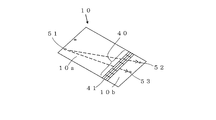
- FIG. 5 is an explanatory diagram showing an embodiment of a printed wiring board 10 for simulation of transmission characteristics.
- the EBG structure 40 is a structure in which three EBG unit cells 41 are arranged in the longitudinal direction of the printed wiring board 10 and 24 in the cross-sectional direction.
- the longitudinal direction of the printed wiring board 10 is the same as the direction along the branch of the EBG unit cell 41.
- the EBG unit cell 41 has the same shape as that shown in FIG. 2A described above, the thickness between the power supply layer electrode and the capacitive coupling element is 12 ⁇ m, and the EBG unit cell 41 is formed with a 2.0 mm square. Is done.
- the width of the EBG structure 40 is 6.0 mm in the longitudinal direction and 48.0 mm in the cross-sectional direction.
- the ground layer and the insulating layer in the thickness direction of the printed wiring board 10 are omitted.
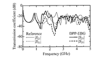
- FIG. 6 shows the results of evaluating the transmission characteristics between the port 51 and the port 52 and the port 51 and the port 53 in the electromagnetic field simulation using the printed wiring board 10.
- the thick line indicates the transmission characteristic when the EBG structure 40 is provided, and the thin line indicates the transmission characteristic when there is no EBG structure 40 (solid structure) (Reference).
- S21 indicates between the port 51 and the port 52, and S31 indicates between the port 51 and the port 53.
- the transmission amount is reduced by 20 dB or more in the vicinity of 2.4 GHz, and a blocking region that does not propagate high-frequency electromagnetic noise is formed. From this result, it can be seen that if the power supply layer pattern in the EBG unit cell or the shape of the capacitive coupling element is changed, it is possible to further reduce the size or form the stop band in a different frequency range.
- EBG structure 4 ' according to another embodiment will be described with reference to FIGS. 7 (a) to (c).
- the same members as those in the EBG structure 4 according to the above-described embodiment are denoted by the same reference numerals, and detailed description thereof is omitted.
- the power supply layer pattern 42 ′ connects adjacent EBG unit cells 41 with a branch 45, as shown in FIGS. 7A and 7B, and this branch 45 And a slit 46 and a power supply layer electrode 47 connected at a portion other than the end.
- “other than the end portion” means a portion other than the above-mentioned “end portion”, and from the end (corner) on the opposite side to the via 44a, the position on the via 44a side from the position of about 1/8 of the side length. It means to the end (corner).
- the interlayer thickness between the power supply layer electrode 47 and the capacitive coupling element 43 is 12 ⁇ m.
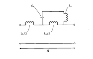
- FIG. 8 is an equivalent circuit of a parallel resonant circuit portion included in the EBG unit cell 41 shown in FIG.
- L b / 2 represents the inductance component of the branch 45.
- Cs represents a coupling capacitance between the power supply layer electrode 47 and the capacitive coupling element 43 obtained by dividing the power supply layer pattern 42 ′ by the slit 46.
- the inductance component is L b / 2.
- the denominator takes different values depending on the connection position.
- FIG. 9 is a graph showing the electromagnetic field simulation result for obtaining the resonance frequency of the parallel resonance circuit in the EBG structure 4 ′ shown in FIG. From this resonance analysis result, it can be seen that the EBG structure 4 ′ can set a blocking region for suppressing electromagnetic noise propagation in a band near 3.3 GHz.
- the “edge” graph shows the result of the EBG unit cell 41 (12 ⁇ m thickness) described above.
- the EBG structure (EBG unit cell) can be reduced in size even though the EBG structure does not have a power supply layer and a ground via. Furthermore, since the EBG structure is installed in the printed wiring board at the design stage, the mounting cost after manufacturing the printed wiring board becomes unnecessary.
- the applied frequency can be changed by a relatively easy design change in which the connection position is changed.
- the branch may be placed anywhere in the EBG unit cell.
- the branch 45 ′ is disposed at a substantially central portion of the EBG unit cell 41.
- the same members as those in the EBG structure 4 according to the above-described embodiment are denoted by the same reference numerals, and detailed description thereof is omitted.
Landscapes
- Engineering & Computer Science (AREA)
- Microelectronics & Electronic Packaging (AREA)
- Physics & Mathematics (AREA)
- Electromagnetism (AREA)
- Theoretical Computer Science (AREA)
- General Engineering & Computer Science (AREA)
- General Physics & Mathematics (AREA)
- Manufacturing & Machinery (AREA)
- Structure Of Printed Boards (AREA)
- Production Of Multi-Layered Print Wiring Board (AREA)
Abstract
Description
2 電源層
3 グラウンド層
4、4’、4’’、40 EBG構造
41 EBG単位セル
42、42’ 電源層パターン
43 容量結合素子
44、44a、44b ビア
45、45’ ブランチ
46 スリット
47 電源層電極
51~53 ポート
9 絶縁層
Claims (5)
- 電源層とグラウンド層とを含み、
電源層の一部に形成される電源層パターンが、隣接するEBG単位セル間を接続する直流給電路であるブランチと、このブランチに沿って設けられたスリットを介して接続する電源層電極を含み、
前記電源層電極と対向するよう層間を設けて配置される容量結合素子が、前記電源層パターン内のブランチと、ビアを介して接続されるEBG単位セルが周期的に配置された構造を有することを特徴とする印刷配線板。 - 電源層パターンが、前記ブランチと前記スリットを介して端部で接続する電源層電極を含む請求項1に記載の印刷配線板。
- 電源層パターンが、前記ブランチと前記スリットを介して端部以外で接続する電源層電極を含む請求項1に記載の印刷配線板。
- 前記ブランチがEBG単位セルの端部に配置される請求項1~3のいずれかに記載の印刷配線板。
- 前記電源層電極と前記容量結合素子との層間の厚さが25μm以下である請求項1~4のいずれかに記載の印刷配線板。
Priority Applications (4)
| Application Number | Priority Date | Filing Date | Title |
|---|---|---|---|
| KR1020197002278A KR102188294B1 (ko) | 2016-07-27 | 2017-07-20 | 인쇄 배선판 |
| CN201780046115.6A CN109496460B (zh) | 2016-07-27 | 2017-07-20 | 印刷布线板 |
| JP2018529827A JP6611066B2 (ja) | 2016-07-27 | 2017-07-20 | 印刷配線板 |
| US16/320,399 US10542622B2 (en) | 2016-07-27 | 2017-07-20 | Printed wiring board |
Applications Claiming Priority (4)
| Application Number | Priority Date | Filing Date | Title |
|---|---|---|---|
| JP2016-147671 | 2016-07-27 | ||
| JP2016147671 | 2016-07-27 | ||
| JP2017-013647 | 2017-01-27 | ||
| JP2017013647 | 2017-01-27 |
Publications (1)
| Publication Number | Publication Date |
|---|---|
| WO2018021150A1 true WO2018021150A1 (ja) | 2018-02-01 |
Family
ID=61016164
Family Applications (1)
| Application Number | Title | Priority Date | Filing Date |
|---|---|---|---|
| PCT/JP2017/026331 Ceased WO2018021150A1 (ja) | 2016-07-27 | 2017-07-20 | 印刷配線板 |
Country Status (6)
| Country | Link |
|---|---|
| US (1) | US10542622B2 (ja) |
| JP (1) | JP6611066B2 (ja) |
| KR (1) | KR102188294B1 (ja) |
| CN (1) | CN109496460B (ja) |
| TW (1) | TWI658768B (ja) |
| WO (1) | WO2018021150A1 (ja) |
Cited By (2)
| Publication number | Priority date | Publication date | Assignee | Title |
|---|---|---|---|---|
| JP2018073956A (ja) * | 2016-10-27 | 2018-05-10 | 京セラ株式会社 | 中継用印刷配線板 |
| JP2018142684A (ja) * | 2017-02-24 | 2018-09-13 | 京セラ株式会社 | 印刷配線板 |
Families Citing this family (1)
| Publication number | Priority date | Publication date | Assignee | Title |
|---|---|---|---|---|
| KR102273378B1 (ko) * | 2019-12-17 | 2021-07-06 | 국방기술품질원 | 전자기 밴드갭 구조물 |
Citations (2)
| Publication number | Priority date | Publication date | Assignee | Title |
|---|---|---|---|---|
| JP2008131509A (ja) * | 2006-11-22 | 2008-06-05 | Nec Tokin Corp | Ebg構造体及びノイズフィルタ |
| JP2013232613A (ja) * | 2012-04-05 | 2013-11-14 | Sony Corp | 配線基板及び電子機器 |
Family Cites Families (27)
| Publication number | Priority date | Publication date | Assignee | Title |
|---|---|---|---|---|
| US7626216B2 (en) * | 2005-10-21 | 2009-12-01 | Mckinzie Iii William E | Systems and methods for electromagnetic noise suppression using hybrid electromagnetic bandgap structures |
| JP2007228222A (ja) * | 2006-02-23 | 2007-09-06 | Mitsubishi Electric Corp | Ebgマテリアル |
| TW200818451A (en) * | 2006-06-02 | 2008-04-16 | Renesas Tech Corp | Semiconductor device |
| TW200808136A (en) | 2006-07-26 | 2008-02-01 | Inventec Corp | A layout design for a multilayer printed circuit board |
| US20080158840A1 (en) * | 2006-12-27 | 2008-07-03 | Inventec Corporation | DC power plane structure |
| US7839654B2 (en) * | 2007-02-28 | 2010-11-23 | International Business Machines Corporation | Method for ultimate noise isolation in high-speed digital systems on packages and printed circuit boards (PCBS) |
| KR100851076B1 (ko) * | 2007-04-30 | 2008-08-12 | 삼성전기주식회사 | 전자기 밴드갭 구조물 및 인쇄회로기판 |
| KR100871346B1 (ko) * | 2007-06-22 | 2008-12-01 | 삼성전기주식회사 | 전자기 밴드갭 구조물 및 인쇄회로기판 |
| JP5662801B2 (ja) * | 2007-11-16 | 2015-02-04 | ホリンワース ファンド,エル.エル.シー. | フィルタ設計方法およびメタマテリアル構造ベースのフィルタ |
| JP5380919B2 (ja) | 2008-06-24 | 2014-01-08 | 日本電気株式会社 | 導波路構造およびプリント配線板 |
| US20100060527A1 (en) * | 2008-09-10 | 2010-03-11 | International Business Machines Corporation | Electromagnetic band gap tuning using undulating branches |
| US8288660B2 (en) * | 2008-10-03 | 2012-10-16 | International Business Machines Corporation | Preserving stopband characteristics of electromagnetic bandgap structures in circuit boards |
| KR100999550B1 (ko) | 2008-10-08 | 2010-12-08 | 삼성전기주식회사 | 전자기 밴드갭 구조물 |
| DE102008051531B4 (de) * | 2008-10-14 | 2013-04-18 | Fraunhofer-Gesellschaft zur Förderung der angewandten Forschung e.V. | Elektrisches System mit einer Vorrichtung zur Unterdrückung der Ausbreitung einer elektromagnetischen Störung |
| KR101018796B1 (ko) * | 2008-12-02 | 2011-03-03 | 삼성전기주식회사 | 전자기 밴드갭 구조물 및 회로 기판 |
| KR101055483B1 (ko) * | 2009-04-07 | 2011-08-08 | 포항공과대학교 산학협력단 | 전자기 밴드갭 구조물 및 이를 포함하는 인쇄회로기판 |
| WO2010125784A1 (ja) * | 2009-04-30 | 2010-11-04 | 日本電気株式会社 | 構造体、プリント基板、アンテナ、伝送線路導波管変換器、アレイアンテナ、電子装置 |
| CN101667567B (zh) | 2009-07-06 | 2011-08-17 | 深圳先进技术研究院 | 电磁干扰隔离装置 |
| KR101308970B1 (ko) * | 2009-12-21 | 2013-09-17 | 한국전자통신연구원 | 불요 전자파 및 노이즈 억제를 위한 다층 인쇄 회로 기판 |
| JP2013058585A (ja) | 2011-09-08 | 2013-03-28 | Oki Printed Circuits Co Ltd | 多層プリント配線板 |
| JP2013183082A (ja) | 2012-03-02 | 2013-09-12 | Oki Printed Circuits Co Ltd | 多層プリント配線板 |
| JP5694251B2 (ja) | 2012-07-27 | 2015-04-01 | 株式会社東芝 | Ebg構造体および回路基板 |
| KR20140102462A (ko) * | 2013-02-14 | 2014-08-22 | 한국전자통신연구원 | 전자기 밴드갭 구조물 및 상기 전자기 밴드갭 구조물의 제조 방법 |
| JP5660168B2 (ja) | 2013-07-25 | 2015-01-28 | 日本電気株式会社 | 導波路構造、プリント配線板、及びそれを用いた電子装置 |
| JP6168943B2 (ja) * | 2013-09-20 | 2017-07-26 | 株式会社東芝 | Ebg構造体、半導体デバイスおよび回路基板 |
| WO2015122203A1 (ja) * | 2014-02-12 | 2015-08-20 | 株式会社村田製作所 | プリント基板 |
| JP6894602B2 (ja) * | 2014-11-28 | 2021-06-30 | 国立大学法人 岡山大学 | 印刷配線板およびその製造方法 |
-
2017
- 2017-07-20 CN CN201780046115.6A patent/CN109496460B/zh active Active
- 2017-07-20 WO PCT/JP2017/026331 patent/WO2018021150A1/ja not_active Ceased
- 2017-07-20 JP JP2018529827A patent/JP6611066B2/ja active Active
- 2017-07-20 US US16/320,399 patent/US10542622B2/en active Active
- 2017-07-20 KR KR1020197002278A patent/KR102188294B1/ko active Active
- 2017-07-26 TW TW106125104A patent/TWI658768B/zh active
Patent Citations (2)
| Publication number | Priority date | Publication date | Assignee | Title |
|---|---|---|---|---|
| JP2008131509A (ja) * | 2006-11-22 | 2008-06-05 | Nec Tokin Corp | Ebg構造体及びノイズフィルタ |
| JP2013232613A (ja) * | 2012-04-05 | 2013-11-14 | Sony Corp | 配線基板及び電子機器 |
Cited By (2)
| Publication number | Priority date | Publication date | Assignee | Title |
|---|---|---|---|---|
| JP2018073956A (ja) * | 2016-10-27 | 2018-05-10 | 京セラ株式会社 | 中継用印刷配線板 |
| JP2018142684A (ja) * | 2017-02-24 | 2018-09-13 | 京セラ株式会社 | 印刷配線板 |
Also Published As
| Publication number | Publication date |
|---|---|
| CN109496460B (zh) | 2021-09-21 |
| CN109496460A (zh) | 2019-03-19 |
| JPWO2018021150A1 (ja) | 2019-07-18 |
| KR102188294B1 (ko) | 2020-12-08 |
| US20190274214A1 (en) | 2019-09-05 |
| KR20190021401A (ko) | 2019-03-05 |
| TW201811141A (zh) | 2018-03-16 |
| TWI658768B (zh) | 2019-05-01 |
| JP6611066B2 (ja) | 2019-11-27 |
| US10542622B2 (en) | 2020-01-21 |
Similar Documents
| Publication | Publication Date | Title |
|---|---|---|
| US8779874B2 (en) | Waveguide structure and printed-circuit board | |
| US9184720B2 (en) | High-frequency laminated component and laminated high-frequency filter | |
| US11742558B2 (en) | Filter | |
| JP6611066B2 (ja) | 印刷配線板 | |
| TW201640978A (zh) | 印刷佈線板及其製造方法 | |
| JP2015061258A (ja) | Ebg構造体、半導体デバイスおよび回路基板 | |
| JP2009054876A (ja) | プリント配線板 | |
| WO2016047234A1 (ja) | 小型スロット型アンテナ | |
| US9148108B2 (en) | Band pass filter | |
| US20150236393A1 (en) | Multilayer circuit substrate | |
| TWI659676B (zh) | 印刷配線板 | |
| US9674942B2 (en) | Structure, wiring board and electronic device | |
| JP5542231B1 (ja) | 多層回路基板 | |
| JP6333048B2 (ja) | 多層回路基板 | |
| JP6884616B2 (ja) | 印刷配線板 | |
| JP2008294816A (ja) | 電子部品 | |
| JP4502937B2 (ja) | 積層ストリップラインフィルタ | |
| JP4810925B2 (ja) | 半導体パッケージ、半導体装置及び電子機器 | |
| WO2020105396A1 (ja) | フィルタ | |
| Ali et al. | Investigation of misalignment in microwave multilayer filters | |
| Ali et al. | Influence of the fabrication errors on IC multilayer filter circuits |
Legal Events
| Date | Code | Title | Description |
|---|---|---|---|
| 121 | Ep: the epo has been informed by wipo that ep was designated in this application |
Ref document number: 17834158 Country of ref document: EP Kind code of ref document: A1 |
|
| ENP | Entry into the national phase |
Ref document number: 20197002278 Country of ref document: KR Kind code of ref document: A |
|
| ENP | Entry into the national phase |
Ref document number: 2018529827 Country of ref document: JP Kind code of ref document: A |
|
| NENP | Non-entry into the national phase |
Ref country code: DE |
|
| 122 | Ep: pct application non-entry in european phase |
Ref document number: 17834158 Country of ref document: EP Kind code of ref document: A1 |