WO2018020876A1 - 給電装置 - Google Patents
給電装置 Download PDFInfo
- Publication number
- WO2018020876A1 WO2018020876A1 PCT/JP2017/021797 JP2017021797W WO2018020876A1 WO 2018020876 A1 WO2018020876 A1 WO 2018020876A1 JP 2017021797 W JP2017021797 W JP 2017021797W WO 2018020876 A1 WO2018020876 A1 WO 2018020876A1
- Authority
- WO
- WIPO (PCT)
- Prior art keywords
- power
- coil
- power supply
- resonance
- frequency
- Prior art date
Links
- 238000004891 communication Methods 0.000 claims abstract description 94
- 238000005259 measurement Methods 0.000 claims description 64
- 230000000694 effects Effects 0.000 abstract description 6
- 238000001514 detection method Methods 0.000 description 224
- 230000004048 modification Effects 0.000 description 28
- 238000012986 modification Methods 0.000 description 28
- 102100035954 Choline transporter-like protein 2 Human genes 0.000 description 26
- 101000948115 Homo sapiens Choline transporter-like protein 2 Proteins 0.000 description 26
- 238000010586 diagram Methods 0.000 description 21
- 230000006870 function Effects 0.000 description 20
- 230000008859 change Effects 0.000 description 12
- 102100031699 Choline transporter-like protein 1 Human genes 0.000 description 11
- 101000940912 Homo sapiens Choline transporter-like protein 1 Proteins 0.000 description 11
- 238000000034 method Methods 0.000 description 10
- 229910052751 metal Inorganic materials 0.000 description 8
- 239000002184 metal Substances 0.000 description 8
- 238000010408 sweeping Methods 0.000 description 7
- 230000005672 electromagnetic field Effects 0.000 description 6
- 230000007274 generation of a signal involved in cell-cell signaling Effects 0.000 description 6
- 238000012545 processing Methods 0.000 description 6
- 238000010168 coupling process Methods 0.000 description 5
- 238000005516 engineering process Methods 0.000 description 5
- 230000008569 process Effects 0.000 description 5
- 230000008878 coupling Effects 0.000 description 4
- 238000005859 coupling reaction Methods 0.000 description 4
- 230000005674 electromagnetic induction Effects 0.000 description 4
- 238000012840 feeding operation Methods 0.000 description 4
- 230000004907 flux Effects 0.000 description 4
- 230000009471 action Effects 0.000 description 2
- 230000004913 activation Effects 0.000 description 2
- 230000002238 attenuated effect Effects 0.000 description 2
- 230000005540 biological transmission Effects 0.000 description 2
- 230000005684 electric field Effects 0.000 description 2
- 230000010365 information processing Effects 0.000 description 2
- 238000009774 resonance method Methods 0.000 description 2
- 230000004044 response Effects 0.000 description 2
- 238000012546 transfer Methods 0.000 description 2
- HBBGRARXTFLTSG-UHFFFAOYSA-N Lithium ion Chemical compound [Li+] HBBGRARXTFLTSG-UHFFFAOYSA-N 0.000 description 1
- 239000003990 capacitor Substances 0.000 description 1
- 238000013461 design Methods 0.000 description 1
- 230000006872 improvement Effects 0.000 description 1
- 229910001416 lithium ion Inorganic materials 0.000 description 1
- 238000004519 manufacturing process Methods 0.000 description 1
- 239000000463 material Substances 0.000 description 1
- 230000001151 other effect Effects 0.000 description 1
- 239000000126 substance Substances 0.000 description 1
Images


Classifications
-
- H—ELECTRICITY
- H04—ELECTRIC COMMUNICATION TECHNIQUE
- H04B—TRANSMISSION
- H04B5/00—Near-field transmission systems, e.g. inductive or capacitive transmission systems
- H04B5/70—Near-field transmission systems, e.g. inductive or capacitive transmission systems specially adapted for specific purposes
- H04B5/79—Near-field transmission systems, e.g. inductive or capacitive transmission systems specially adapted for specific purposes for data transfer in combination with power transfer
-
- H—ELECTRICITY
- H01—ELECTRIC ELEMENTS
- H01M—PROCESSES OR MEANS, e.g. BATTERIES, FOR THE DIRECT CONVERSION OF CHEMICAL ENERGY INTO ELECTRICAL ENERGY
- H01M10/00—Secondary cells; Manufacture thereof
- H01M10/42—Methods or arrangements for servicing or maintenance of secondary cells or secondary half-cells
- H01M10/46—Accumulators structurally combined with charging apparatus
-
- H—ELECTRICITY
- H02—GENERATION; CONVERSION OR DISTRIBUTION OF ELECTRIC POWER
- H02J—CIRCUIT ARRANGEMENTS OR SYSTEMS FOR SUPPLYING OR DISTRIBUTING ELECTRIC POWER; SYSTEMS FOR STORING ELECTRIC ENERGY
- H02J50/00—Circuit arrangements or systems for wireless supply or distribution of electric power
- H02J50/10—Circuit arrangements or systems for wireless supply or distribution of electric power using inductive coupling
- H02J50/12—Circuit arrangements or systems for wireless supply or distribution of electric power using inductive coupling of the resonant type
-
- H—ELECTRICITY
- H02—GENERATION; CONVERSION OR DISTRIBUTION OF ELECTRIC POWER
- H02J—CIRCUIT ARRANGEMENTS OR SYSTEMS FOR SUPPLYING OR DISTRIBUTING ELECTRIC POWER; SYSTEMS FOR STORING ELECTRIC ENERGY
- H02J50/00—Circuit arrangements or systems for wireless supply or distribution of electric power
- H02J50/60—Circuit arrangements or systems for wireless supply or distribution of electric power responsive to the presence of foreign objects, e.g. detection of living beings
-
- H—ELECTRICITY
- H02—GENERATION; CONVERSION OR DISTRIBUTION OF ELECTRIC POWER
- H02J—CIRCUIT ARRANGEMENTS OR SYSTEMS FOR SUPPLYING OR DISTRIBUTING ELECTRIC POWER; SYSTEMS FOR STORING ELECTRIC ENERGY
- H02J50/00—Circuit arrangements or systems for wireless supply or distribution of electric power
- H02J50/80—Circuit arrangements or systems for wireless supply or distribution of electric power involving the exchange of data, concerning supply or distribution of electric power, between transmitting devices and receiving devices
-
- H—ELECTRICITY
- H02—GENERATION; CONVERSION OR DISTRIBUTION OF ELECTRIC POWER
- H02J—CIRCUIT ARRANGEMENTS OR SYSTEMS FOR SUPPLYING OR DISTRIBUTING ELECTRIC POWER; SYSTEMS FOR STORING ELECTRIC ENERGY
- H02J7/00—Circuit arrangements for charging or depolarising batteries or for supplying loads from batteries
-
- H—ELECTRICITY
- H04—ELECTRIC COMMUNICATION TECHNIQUE
- H04B—TRANSMISSION
- H04B5/00—Near-field transmission systems, e.g. inductive or capacitive transmission systems
- H04B5/40—Near-field transmission systems, e.g. inductive or capacitive transmission systems characterised by components specially adapted for near-field transmission
- H04B5/48—Transceivers
-
- H—ELECTRICITY
- H01—ELECTRIC ELEMENTS
- H01M—PROCESSES OR MEANS, e.g. BATTERIES, FOR THE DIRECT CONVERSION OF CHEMICAL ENERGY INTO ELECTRICAL ENERGY
- H01M2220/00—Batteries for particular applications
- H01M2220/30—Batteries in portable systems, e.g. mobile phone, laptop
-
- H—ELECTRICITY
- H03—ELECTRONIC CIRCUITRY
- H03H—IMPEDANCE NETWORKS, e.g. RESONANT CIRCUITS; RESONATORS
- H03H3/00—Apparatus or processes specially adapted for the manufacture of impedance networks, resonating circuits, resonators
- H03H3/007—Apparatus or processes specially adapted for the manufacture of impedance networks, resonating circuits, resonators for the manufacture of electromechanical resonators or networks
- H03H3/02—Apparatus or processes specially adapted for the manufacture of impedance networks, resonating circuits, resonators for the manufacture of electromechanical resonators or networks for the manufacture of piezoelectric or electrostrictive resonators or networks
- H03H3/04—Apparatus or processes specially adapted for the manufacture of impedance networks, resonating circuits, resonators for the manufacture of electromechanical resonators or networks for the manufacture of piezoelectric or electrostrictive resonators or networks for obtaining desired frequency or temperature coefficient
- H03H2003/0414—Resonance frequency
-
- Y—GENERAL TAGGING OF NEW TECHNOLOGICAL DEVELOPMENTS; GENERAL TAGGING OF CROSS-SECTIONAL TECHNOLOGIES SPANNING OVER SEVERAL SECTIONS OF THE IPC; TECHNICAL SUBJECTS COVERED BY FORMER USPC CROSS-REFERENCE ART COLLECTIONS [XRACs] AND DIGESTS
- Y02—TECHNOLOGIES OR APPLICATIONS FOR MITIGATION OR ADAPTATION AGAINST CLIMATE CHANGE
- Y02E—REDUCTION OF GREENHOUSE GAS [GHG] EMISSIONS, RELATED TO ENERGY GENERATION, TRANSMISSION OR DISTRIBUTION
- Y02E60/00—Enabling technologies; Technologies with a potential or indirect contribution to GHG emissions mitigation
- Y02E60/10—Energy storage using batteries
Definitions
- the present disclosure relates to a power feeding device that wirelessly supplies power to a power receiving device.
- a mobile phone can be charged by placing a mobile phone (power receiving device) on a power supply tray (power supply device).
- Examples of a method for performing such wireless power feeding include an electromagnetic induction method and a magnetic field resonance method using a resonance phenomenon.
- the electromagnetic induction method and the magnetic field resonance method are often collectively referred to as a magnetic field coupling method.
- Patent Documents 1 to 3 disclose power supply systems that can detect foreign matter.
- the first power supply device includes a power supply unit, a communication unit, and a control unit.
- the power feeding unit wirelessly supplies power to a power receiving device having a power receiving coil.
- the communication unit receives coil information transmitted from the power receiving apparatus and indicating whether or not a coil is provided in the vicinity of the power receiving coil.
- the control unit makes a first determination as to whether or not to supply power to the power receiving device based on the coil information, and controls the operation of the power supply unit based on the result of the first determination.
- the second power supply device includes a power supply unit, a first measurement unit, and a control unit.
- the power supply unit wirelessly supplies power to the power receiving device using a power supply coil.
- the first measurement unit measures the first frequency characteristic of the first parameter in the first frequency range based on a signal in the power supply coil or a measurement coil provided in the vicinity of the power supply coil.
- the control unit makes a first determination as to whether or not to supply power to the power receiving device based on the first frequency characteristic, and controls the operation of the power feeding unit based on the result of the first determination It is.
- a first determination is made as to whether or not power is supplied to the power receiving device, and power is supplied to the power receiving device based on the first determination result. Is done. This first determination is made based on the coil information transmitted from the power receiving apparatus. This coil information indicates whether a coil is provided in the vicinity of the power receiving coil.
- a first determination is made as to whether power is supplied to the power receiving device, and power is supplied to the power receiving device based on the first determination result. Is done. This first determination is made based on the first frequency characteristic. The first frequency characteristic is measured based on a signal in a feeding coil or a measuring coil provided in the vicinity of the feeding coil.
- the first power supply device in one embodiment of the present disclosure, power is transmitted to the power receiving device based on the coil information transmitted from the power receiving device and indicating whether or not a coil is provided in the vicinity of the power receiving coil. Since the first determination as to whether or not to supply is made, safety can be improved.
- the first frequency characteristic is measured based on the signal in the power supply coil or the measurement coil provided in the vicinity of the power supply coil, and the first frequency characteristic. Since the first determination as to whether or not to supply power to the power receiving device is made based on the above, safety can be improved.
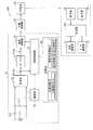
- FIG. 2 is a block diagram illustrating a configuration example of a power feeding device illustrated in FIG. 1.
- FIG. 3 is an explanatory diagram illustrating an operation example of the power feeding device illustrated in FIG. 2. It is a block diagram showing the example of 1 structure of the smart phone shown in FIG. It is a block diagram showing the example of 1 structure of the other smart phone shown in FIG. It is explanatory drawing showing an example of arrangement
- positioning of the feeding coil and coil shown to FIG. 4B. 3 is a flowchart illustrating an operation example of the power feeding system illustrated in FIG. 1.
- FIG. 1 is a flowchart illustrating an operation example of the power feeding system illustrated in FIG. 1.
- FIG. 2 is a sequence diagram illustrating an example of a communication operation in the power supply system illustrated in FIG. 1. It is explanatory drawing showing the example of 1 operation
- FIG. 10 is an explanatory diagram illustrating another operation example of the power feeding system illustrated in FIG. 1.
- FIG. 11 is a characteristic diagram illustrating a characteristic example in the operation example illustrated in FIG. 10.
- FIG. 11 is another characteristic diagram illustrating a characteristic example in the operation example illustrated in FIG. 10.
- FIG. 10 is an explanatory diagram illustrating another operation example of the power feeding system illustrated in FIG. 1.
- FIG. 10 is an explanatory diagram illustrating another operation example of the power feeding system illustrated in FIG. 1.
- FIG. 14 is a characteristic diagram illustrating a characteristic example in the operation example illustrated in FIG. 13.
- FIG. 14 is a characteristic diagram illustrating a characteristic example in the operation example illustrated in FIG. 13.
- FIG. 14 is another characteristic diagram illustrating a characteristic example in the operation example illustrated in FIG. 13. It is a block diagram showing the example of 1 structure of the electric power feeder which concerns on a modification.
- FIG. 16 is an explanatory diagram illustrating an operation example of the power feeding device illustrated in FIG. 15. It is a block diagram showing the example of 1 structure of the electric power feeder which concerns on another modification.
- FIG. 18 is an explanatory diagram illustrating an operation example of the power feeding device illustrated in FIG. 17. It is a block diagram showing the example of 1 structure of the smart phone which concerns on another modification. It is a flowchart showing the operation example of the electric power feeding system which concerns on another modification. It is a block diagram showing the example of 1 structure of the smart phone which concerns on another modification.
- FIG. 1 illustrates a configuration example of a power feeding system (power feeding system 1) according to an embodiment.
- the power supply system 1 detects whether a foreign object such as a metal piece, an IC tag or an IC card having a coil, or the like is sandwiched between a power supply device and a power reception device before power supply.
- the power feeding system 1 includes a power feeding device 10 and a smartphone 20.
- the smartphone 20 has a power receiving device 30.
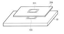
- the power supply device 10 is a tray-type power supply device. By placing the smartphone 20 on the power supply surface of the power supply device 10, the power supply device 10 supplies power to the power reception device 30 of the smartphone 20, and the secondary battery 29. (To be described later) can be charged.
- a power feeding coil 123 (described later) is arranged on the power feeding surface (side in contact with the smartphone 20) of the power feeding device 10, and the power receiving surface (side in contact with the power feeding device 10) of the smartphone 20 receives power received by the power receiving device 30.
- a coil 311 (described later) is arranged.
- the power feeding device 10 supplies power to the power receiving device 30 of the smartphone 20 through the power feeding coil 123 and the power receiving coil 311 by electromagnetic induction.
- the user can charge the secondary battery 29 without directly connecting an AC (Alternating Current) adapter or the like to the smartphone 20.
- the power feeding system 1 can improve user convenience.
- the power supply apparatus 10 detects whether or not there is a foreign object such as a metal piece between the power supply apparatus 10 and the power receiving apparatus 30 before performing the main power supply (foreign object detection (FOD: Foreign). (Object Detection) DF1, DF2), and also has a function of detecting whether there is an IC tag or IC card having a coil between the power feeding device 10 and the power receiving device 30 (resonance detection DR1, DR2). Yes. That is, for example, when there is a foreign object such as a metal piece between the power feeding device 10 and the power receiving device 30, an eddy current flows through the metal piece when the power feeding device 10 supplies power to the power receiving device 30. Otherwise, the metal piece may generate heat.
- the power supply apparatus 10 performs foreign matter detection DF1 and DF2 and resonance detection DR1 and DR2, and after confirming that there is no foreign matter such as a metal piece, an IC tag or an IC card having a coil, etc., starts this power supply. . Thereby, in the electric power feeding system 1, safety can be improved.
- power is supplied to the smartphone 20, but the present invention is not limited to this.
- a digital camera, a video camera, a mobile phone, a smartphone, a mobile battery, a tablet, an e-book reader Power can be supplied to various electronic devices such as an audio player.
- the power supply apparatus 10 supplies power to one smartphone 20.
- the power supply apparatus 10 is not limited to this. Instead, the power supply apparatus 10 can simultaneously supply power to two or more electronic devices. Alternatively, power may be supplied in a time division manner (sequentially).
- FIG. 2 illustrates a configuration example of the power supply apparatus 10.
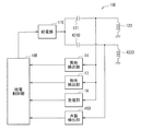
- the power supply device 10 includes a power supply unit 11, a capacitive element 121, a switch 122, a power supply coil 123, an object detection unit 13, a foreign object detection unit 14, a resonance detection unit 15, a reception unit 16, and a power supply control unit. 19.
- the power supply unit 11 generates an AC power signal SP1 based on an instruction from the power supply control unit 19.
- the power supply unit 11 is supplied with AC power via a plug socket (so-called outlet), or is supplied with AC power or DC power from another power supply device.
- the electric power feeding part 11 produces
- the frequency of the power signal SP1 is, for example, about 100 kHz to several hundred kHz.
- the power supply unit 11 also has a function of generating an AC signal SDF having power lower than that of the power signal SP1 in the foreign object detection DF1.
- the electric power feeding part 11 sweeps the frequency of AC signal SDF over the predetermined
- the frequency sweep range RDF includes the frequency of the power signal SP1, but is not limited thereto, and may not include the frequency of the power signal SP1. In this case, it is desirable that the frequency sweep range RDF is close to the frequency of the power signal SP1.
- the power supply unit 11 also has a function of generating an AC signal SDR having a power lower than that of the power signal SP1 in the resonance detection DR1. At that time, the power supply unit 11 sweeps the frequency of the AC signal SDR over a predetermined frequency range (frequency sweep range RDR) including the frequency fc (for example, 13.56 MHz) of a carrier wave used by an IC tag, an IC card, or the like. It has become.
- the frequency sweep range RDR may include a frequency higher than the maximum frequency in the frequency sweep range RDF, for example.
- the power supply unit 11 also has a function of transmitting a power supply control signal CTL1 to the power receiving device 30. Specifically, when the power supply unit 11 transmits the power supply control signal CTL1, the power supply unit 11 generates the power signal SP1 and modulates the power signal SP1 according to the information to be transmitted. Thereby, the communication part 35 (after-mentioned) of the power receiving apparatus 30 can receive electric power feeding control signal CTL1 based on the modulated electric power signal.
- One end of the capacitive element 121 is connected to one end of the switch 122 and the power supply unit 11, and the other end is connected to the other end of the switch 122 and one end of the power supply coil 123.
- One end of the switch 122 is connected to one end of the capacitive element 121 and the power supply unit 11, and the other end is connected to the other end of the capacitive element 121 and one end of the power supply coil 123.
- the switch 122 is turned on / off based on an instruction from the power supply control unit 19.
- the power supply coil 123 is disposed on the power supply surface of the power supply apparatus 10, one end is connected to the other end of the capacitive element 121 and the other end of the switch 122, and the other end is grounded.
- FIG. 3 schematically illustrates an operation example of the power supply unit 11 and the switch 122.
- the switch 122 is turned off based on an instruction from the power supply control unit 19.
- the capacitive element 121 and the feeding coil 123 are connected in series to form a resonance circuit.
- the resonance frequency of this resonance circuit is a frequency near the frequency of the power signal SP1.
- the electric power feeding part 11 supplies electric power signal SP1 to this resonance circuit.
- the feeding coil 123 generates an electromagnetic field according to the power signal SP1.
- the switch 122 When the power supply apparatus 10 performs the foreign object detection DF1, the switch 122 is turned off based on an instruction from the power supply control unit 19. At this time, the capacitive element 121 and the feeding coil 123 constitute a resonance circuit.
- the power supply unit 11 supplies the AC signal SDF to the resonance circuit while sweeping the frequency of the AC signal SDF over the frequency sweep range RDF. Thereby, the feeding coil 123 generates an electromagnetic field corresponding to the AC signal SDF.
- the switch 122 is turned on based on an instruction from the power supply control unit 19. At this time, both ends of the capacitive element 121 are short-circuited by the switch 122.
- the power supply unit 11 supplies the AC signal SDR to the power supply coil 123 while sweeping the frequency of the AC signal SDR over the frequency sweep range RDR. Thereby, the feeding coil 123 generates an electromagnetic field according to the AC signal SDR.
- the object detection unit 13 detects whether an object (for example, the smartphone 20) is placed on the power supply surface of the power supply device 10 based on the voltage at one end of the power supply coil 123. Specifically, for example, the object detection unit 13 detects a signal at one end of the power supply coil 123 during a period in which the power supply unit 11 generates an AC signal. At this time, the amplitude and phase of the signal at one end of the power feeding coil 123 change depending on whether or not an object is placed on the power feeding surface of the power feeding device 10. The object detection unit 13 detects the presence or absence of an object by detecting the change in amplitude and the change in phase.
- the object detection unit 13 detects the object based on the voltage at one end of the power supply coil 123, but is not limited to this, and the object detection unit 13 is based on the voltage or current at another node. May be detected.
- the method for detecting an object is not limited to this, and various methods that can detect the presence or absence of an object are applicable.
- the foreign object detection unit 14 performs the foreign object detection DF1 based on the voltage at one end of the feeding coil 123. Specifically, the foreign object detection unit 14 obtains the quality factor QD in the frequency sweep range RDF based on the voltage at one end of the power supply coil 123 during the period in which the power supply unit 11 generates the AC signal SDF.
- the quality factor QD relates to the quality factor of the resonance circuit formed by the power feeding coil 123 and the capacitive element 121, and is related to the power feeding efficiency from the power feeding device 10 to the power receiving device 30.
- the quality factor QD is a parameter that changes according to the resistance value, the inductance value, the capacitance value, and the frequency in the resonance circuit.
- the quality factor QD is the quality factor of the resonance circuit, but is not limited to this, and may be the quality factor of the feeding coil 123 itself.
- the quality factor QD is reduced due to the resistance component of the foreign object.
- the foreign matter detector 14 detects the presence or absence of foreign matter based on the quality factor QD.
- the foreign object detection unit 14 is based on the quality factor QD and the foreign object determination information IF (described later) transmitted from the power receiving device 30 after the power feeding device 10 and the power receiving device 30 start communication. Thus, it also has a function of performing foreign object detection DF2.
- the foreign object detection unit 14 performs the foreign object detection DF1 based on the voltage at one end of the power supply coil 123.
- the present invention is not limited to this, and the voltage and current at other nodes are not limited thereto.
- the foreign object detection DF1 may be performed.
- the resonance detection unit 15 performs resonance detection DR1 based on the voltage at one end of the power supply coil 123. Specifically, the resonance detection unit 15 performs frequency characteristics (impedance characteristics) of the impedance viewed from the resonance detection unit 15 based on the voltage at one end of the power supply coil 123 during the period in which the power supply unit 11 generates the AC signal SDR. ZDR) is measured, and the number of resonance points (resonance number ND) in the frequency sweep range RDR is obtained based on the impedance characteristic ZDR. For example, when there is an IC tag or IC card having a coil between the power supply apparatus 10 and the power receiving apparatus 30, the resonance number ND changes. The resonance detector 15 detects the presence or absence of an IC tag or an IC card based on the resonance number ND.
- the resonance detection unit 15 is based on the resonance number ND and resonance information IR (described later) transmitted from the power receiving device 30 after the power feeding device 10 and the power receiving device 30 start communication. Also, it has a function of performing resonance detection DR2.
- the resonance detection unit 15 performs the resonance detection DR1 based on the voltage at one end of the power supply coil 123.
- the present invention is not limited to this, and the voltage and current at other nodes are not limited thereto.
- the resonance detection DR1 may be performed based on the above.
- the receiving unit 16 receives the power supply control signal CTL2 by performing communication with the power receiving device 30.
- the power supply control signal CTL2 includes information necessary for the power supply operation, such as a request to increase or decrease power supply to the power supply apparatus 10.
- the power supply control signal CTL2 also includes identification information ID, power information IP, foreign matter determination information IF, resonance information IR, and the like, which will be described later.
- the receiving unit 16 receives the power supply control signal CTL2 based on the voltage at one end of the power supply coil 123. Specifically, first, during a period in which the power supply unit 11 generates the power signal SP1, the communication unit 35 (described later) of the power receiving device 30 changes the load viewed from the power supply device 10 according to information to be transmitted. .
- This change in the load appears as a change in the amplitude and phase of the voltage at one end of the power supply coil 123 and a change in the amplitude and phase of the current flowing through the power supply coil 123 in the power supply apparatus 10.
- the receiving unit 16 receives the power supply control signal CTL2 transmitted from the power receiving device 30 by detecting changes in these amplitudes and phases.
- the power feeding control signal CTL2 is transmitted by so-called load modulation.
- the receiving unit 16 has received the power supply control signal CTL2 based on the voltage at one end of the power supply coil 123.
- the present invention is not limited to this, and the voltage or current at other nodes is not limited thereto. Based on this, the power supply control signal CTL2 may be received.
- the power supply control unit 19 controls the operation of the power supply apparatus 10. Specifically, when detecting whether or not an object (such as the smartphone 20) is placed on the power supply surface of the power supply apparatus 10, the power supply control unit 19 performs control so that the switch 122 is turned off.
- the power supply unit 11 is controlled to generate an AC signal, and the object detection unit 13 is controlled to detect the presence or absence of an object.
- the power supply control unit 19 when performing the foreign object detection DF1, performs control so that the switch 122 is turned off, and controls the power supply unit 11 to generate the AC signal SDF. Control to detect the presence or absence of. In addition, when performing the resonance detection DR1, the power supply control unit 19 performs control so that the switch 122 is turned on, and controls the power supply unit 11 to generate the AC signal SDR. Control is performed to detect the presence or absence of a tag or IC card.
- the power supply control unit 19 controls the reception unit 16 to receive the foreign object determination information IF (described later), and the foreign object detection unit 14 controls the foreign object determination information IF. Based on the above, control is performed so as to detect the presence or absence of foreign matter.
- the power supply control unit 19 controls the reception unit 16 to receive resonance information IR (described later), and the resonance detection unit 15 performs an IC tag or the like based on the resonance information IR. Control is performed to detect the presence or absence of an IC card or the like.
- the power supply control unit 19 performs control so that the switch 122 is turned off when performing the main power supply to the power receiving device 30, and the reception unit 16 provides information such as a request to increase or decrease the power supply power.
- the power supply control signal CTL2 is controlled to be received, and the power of the power signal SP1 generated by the power supply unit 11 is controlled based on this request.
- the smartphone 20 does not have a function of performing near field communication (NFC), and the smartphone 20B has a function of performing near field communication.
- NFC near field communication
- FIG. 4A shows a configuration example of the smartphone 20A.
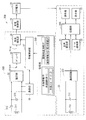
- the smartphone 20A includes a power receiving device 30, a charge control unit 28, a secondary battery 29, a voice communication unit 21, a data communication unit 22, an operation unit 24, a display unit 25, and a processing unit 26A. ing.
- the power receiving device 30 includes a power receiving coil 311, capacitive elements 312 and 313, a rectifying unit 32, a regulator 33, a load connecting unit 34, a communication unit 35, a storage unit 36, and a power receiving control unit 37. Yes.
- the power receiving coil 311 is disposed on the power receiving surface of the smartphone 20, one end is connected to the first input terminal of the rectifying unit 32 via the capacitive element 312, and the other end is connected to the second input terminal of the rectifying unit 32. ing.
- a capacitive element 313 is inserted between the first input terminal and the second input terminal of the rectifying unit 32.
- the power receiving coil 311 and the capacitive element 312 are connected in series to form a resonance circuit.
- the resonance frequency of this resonance circuit is a frequency near the frequency of the power signal SP1.
- the power receiving coil 311 generates an induced voltage corresponding to the change in the magnetic flux in accordance with the electromagnetic induction law based on the electromagnetic field generated by the power feeding coil 123 of the power feeding device 10.
- the circuit including the power receiving coil 311 and the capacitive elements 312 and 313 generates an AC power signal SP2 having a voltage corresponding to the induced voltage between both ends of the power receiving coil 311 and supplies it to the rectifying unit 32 at the time of power feeding. That is, the power signal SP2 is generated based on the power signal SP1 in the power supply apparatus 10.
- the rectifier 32 generates a DC signal having the received voltage Vrect by rectifying the power signal SP2.
- the regulator 33 generates DC power having the voltage Vreg based on the DC signal supplied from the rectifying unit 32.
- the regulator 33 supplies the voltage Vreg as a power supply voltage to each block in the power receiving device 30 and supplies the voltage Vreg to the charge control unit 28 via the load connection unit 34. Yes.
- the load connection unit 34 connects or disconnects the regulator 33 and the charge control unit 28 based on an instruction from the power reception control unit 37.
- the communication unit 35 receives the power supply control signal CTL1 transmitted from the power supply device 10 and transmits the power supply control signal CTL2 including the information supplied from the power reception control unit 37 to the power supply device 10. Specifically, when receiving the power supply control signal CTL1, the communication unit 35 receives the power supply control signal CTL1 by performing a demodulation process on the modulated power signal SP2. Further, when transmitting the power supply control signal CTL2, the communication unit 35 is connected to the first input terminal of the rectifying unit 32 according to the information to be transmitted during the period in which the power supply apparatus 10 is transmitting the power signal SP1. The impedance between the second input terminal is changed. The receiving unit 16 of the power supply apparatus 10 receives the power supply control signal CTL2 by detecting this change in impedance (change in load).
- the storage unit 36 stores information exchanged in the power supply system 1 and is configured using, for example, a nonvolatile memory.
- the storage unit 36 stores identification information ID, power information IP, foreign object determination information IF, and resonance information IR.
- the identification information ID is information for identifying the power receiving device 30 and is, for example, a so-called serial number.
- the power information IP is information indicating the power (power class) that can be received by the power receiving device 30.
- the foreign object determination information IF is information used when the foreign object detection unit 14 of the power supply apparatus 10 performs the foreign object detection DF2, and includes, for example, a reference quality factor Q.
- the resonance information IR is information used when the resonance detection unit 15 of the power supply apparatus 10 performs the resonance detection DR2.
- This resonance information IR includes information about the number of resonance points (resonance number N) in the resonance circuit formed by the coil when the coil is provided in the vicinity of the power receiving coil 311 in the smartphone 20A. .
- the power reception control unit 37 controls the operation of the power receiving device 30. Specifically, the power reception control unit 37 supplies the identification information ID, power information IP, foreign matter determination information IF, and resonance information IR to the communication unit 35, and the communication unit 35 supplies the power supply control signal CTL2 including these pieces of information. Is transmitted to the power supply apparatus 10. In addition, when receiving the power supplied from the power supply apparatus 10, the power reception control unit 37 supplies information about an increase request and a decrease request for the supply power to the communication unit 35 based on the received voltage Vrect, and the communication unit 35. However, the power supply control signal CTL2 including these pieces of information is controlled to be transmitted to the power supply apparatus 10. The power reception control unit 37 controls the operation of connecting or disconnecting the regulator 33 and the charge control unit 28 in the load connection unit 34.
- the charging control unit 28 controls the charging operation in the secondary battery 29.
- the secondary battery 29 stores DC power and is configured using a rechargeable battery such as a lithium ion battery.
- the charge control unit 28 and the secondary battery 29 include various circuits and devices for realizing the function of the smartphone 20 (in this example, the voice communication unit 21, the data communication unit 22, the operation unit 24, the display unit 25, and the processing) Power is supplied to the unit 26A).
- the voice communication unit 21 performs voice communication with a mobile phone base station.
- the data communication unit 22 performs data communication using a wireless LAN (Local Area Network).
- the operation unit 24 is a user interface used when the user operates the smartphone 20A, and includes various buttons and a touch panel.
- the display unit 25 displays the state of the smartphone 20A and various information processing results.
- the processing unit 26A is configured using, for example, a CPU (Central Processing Unit), a RAM (Random Access Memory), a non-volatile memory, and the like, and performs various information processing for realizing the functions of the smartphone 20A by executing a program. Is what you do.
- FIG. 4B shows a configuration example of the smartphone 20B.
- the smartphone 20B includes a power receiving device 30, a charge control unit 28, a secondary battery 29, a voice communication unit 21, a data communication unit 22, an NFC communication unit 23, an operation unit 24, a display unit 25, and a process. Part 26B.
- the smartphone 20B is obtained by adding the NFC communication unit 23 to the smartphone 20A (FIG. 4A) and replacing the processing unit 26A with the processing unit 26B.
- the NFC communication unit 23 performs near field communication.
- the NFC communication unit 23 includes a coil 231, a capacitive element 232, and a communication circuit 233.
- the coil 231 and the capacitive element 232 are connected in parallel to form a resonance circuit.
- the resonance frequency of this resonance circuit is, for example, a frequency near the frequency fc (for example, 13.56 MHz).
- the coil 231 and the capacitive element 232 are connected to the communication circuit 233. Even if a high voltage is generated in the coil 231, the communication circuit 233 is configured not to be destroyed by the high voltage.
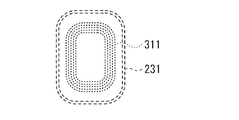
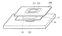
- FIGS. 5 and 6 show arrangement examples of the power receiving coil 311 and the coil 231 in the smartphone 20B.
- the coil 231 is disposed in the vicinity of the power receiving coil 311.
- the power receiving coil 311 and the coil 231 are disposed adjacent to each other on the power receiving surface of the smartphone 20 ⁇ / b> B.
- the center point of the power receiving coil 311 and the center point of the coil 231 are arranged so as to substantially coincide with each other on the power receiving surface of the smartphone 20 ⁇ / b> B.
- the coil diameter of the power receiving coil 311 is smaller than the coil diameter of the coil 231, the power receiving coil 311 is disposed inside the coil 231.
- the coil 231 is provided in the vicinity of the power receiving coil 311.
- the power supply unit 11 corresponds to a specific example of “power supply unit” in the present disclosure.
- the receiving unit 16 corresponds to a specific example of “communication unit” in the present disclosure.
- the coil 231 corresponds to a specific example of “coil” in the present disclosure.
- the resonance information IR corresponds to a specific example of “coil information” in the present disclosure.
- the foreign matter determination information IF corresponds to a specific example of “power receiving coil information” in the present disclosure.
- the resonance detection unit 15 corresponds to a specific example of “first measurement unit” in the present disclosure.
- the foreign object detection unit 14 corresponds to a specific example of “second measurement unit” in the present disclosure.
- the power supply control unit 19 corresponds to a specific example of “a control unit” in the present disclosure.
- the power feeding unit 11 In the power feeding device 10 (FIG. 2), the power feeding unit 11 generates a power signal SP1 and AC signals SDF and SDR based on an instruction from the power feeding control unit 19 and also sends a power feeding control signal CTL1 to the power receiving device 30. Send.
- the switch 122 short-circuits both ends of the capacitive element 121 based on an instruction from the power supply control unit 19.
- the power supply coil 123 generates an electromagnetic field based on the power signal SP1 and the AC signals SDF and SDR.
- the object detection unit 13 detects whether an object is placed on the power supply surface of the power supply apparatus 10.
- the foreign object detection unit 14 detects whether there is a foreign object on the power supply surface of the power supply apparatus 10 by performing foreign object detection DF1 and DF2.
- the resonance detection unit 15 detects whether there is an IC tag or an IC card on the power supply surface of the power supply apparatus 10 by performing resonance detection DR1 and DR2.
- the receiving unit 16 receives the power supply control signal CTL2 transmitted from the power receiving device 30.
- the power supply control unit 19 controls the operation of the power supply apparatus 10.
- the power receiving coil 311 In the power receiving device 30 (FIGS. 4A and 4B), the power receiving coil 311 generates an induced voltage corresponding to the change in the magnetic flux based on the electromagnetic field generated by the power feeding coil 123.
- the power receiving coil 311 and the capacitive elements 312 and 313 supply the rectifying unit 32 with the power signal SP2 corresponding to the power signal SP1.
- the rectifier 32 rectifies the power signal SP2 to generate a DC signal having the received voltage Vrect.
- the regulator 33 generates DC power having the voltage Vreg based on the DC signal supplied from the rectifying unit 32.
- the load connection unit 34 performs connection between the regulator 33 and the charge control unit 28 based on an instruction from the power reception control unit 37.
- the communication unit 35 receives the power supply control signal CTL1 transmitted from the power supply apparatus 10 and transmits a power supply control signal CTL2 including information supplied from the power reception control unit 37 to the power supply apparatus 10.
- the storage unit 36 stores identification information ID, power information IP, foreign object determination information IF, and resonance information IR.
- the power reception control unit 37 controls the operation in the power reception device 30.
- the charging control unit 28 controls the charging operation in the secondary battery 29.
- the secondary battery 29 stores DC power.
- the charge control unit 28 and the secondary battery 29 supply power to various circuits and devices for realizing the function of the smartphone 20 (20A, 20B).
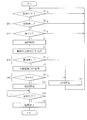
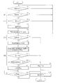
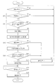
- FIG. 7 shows a flowchart of the power feeding operation in the power feeding system 1.
- the power feeding device 10 performs the foreign object detection DF ⁇ b> 1 and the resonance detection DR ⁇ b> 1, and then starts communication with the power receiving device 30. Then, the power feeding device 10 performs the foreign object detection DF2 and the resonance detection DR2, and then starts the main power feeding to the power receiving device 30. The details will be described below.
- the power supply apparatus 10 detects whether or not an object (for example, the smartphone 20) is placed on the power supply surface of the power supply apparatus 10 (step S1). Specifically, for example, the power supply control unit 19 turns off the switch 122, the power supply unit 11 generates an AC signal, and the object detection unit 13 detects the presence or absence of an object. If there is no object (“N” in step S1), the process returns to step S1, and this step S1 is repeated until an object is detected.
- an object for example, the smartphone 20
- step S2 When an object is detected in step S1 (“Y” in step S1), the power supply apparatus 10 performs foreign object detection DF1 (step S2). Specifically, first, the power supply control unit 19 turns off the switch 122, and the power supply unit 11 generates the AC signal SDF. At that time, the power supply unit 11 sweeps the frequency of the AC signal SDF over the frequency sweep range RDF. And the foreign material detection part 14 calculates
- step S3 When there is no foreign object in step S2 (“Y” in step S2), the power feeding apparatus 10 performs resonance detection DR1 (step S3). Specifically, first, the power supply control unit 19 turns on the switch 122, and the power supply unit 11 generates the AC signal SDR. At that time, the power supply unit 11 sweeps the frequency of the AC signal SDR over the frequency sweep range RDR. Then, the resonance detection unit 15 measures the frequency characteristic (impedance characteristic ZDR) of the impedance viewed from the resonance detection unit 15 in the frequency sweep range RDR, and based on the impedance characteristic ZDR, the resonance point in the frequency sweep range RDR is measured. The number (resonance number ND) is obtained.
- the resonance detector 15 confirms whether or not the resonance number ND is equal to or less than a predetermined threshold value X (ND ⁇ X).
- the predetermined threshold value X is set to “1” in this example.
- power supply apparatus 10 determines that there is an IC tag, an IC card, and the like, and returns to step S1. That is, in this case, the power supply apparatus 10 determines that power should not be supplied because there are IC tags, IC cards, and the like.
- step S3 when the resonance number ND is equal to or less than the predetermined threshold value X (“Y” in step S3), the power feeding device 10 starts communication with the power receiving device 30 (step S4).
- the power supply control unit 19 turns off the switch 122, and the power supply unit 11 generates the power signal SP1.
- the power supply unit 11 supplies the power receiving device 30 with small power that allows the power receiving device 30 to operate.
- the rectifier 32 generates the received voltage Vrect based on the power signal SP2, and the regulator 33 generates the voltage Vreg based on the received voltage Vrect.
- each block of the power receiving device 30 starts operating with the voltage Vreg as a power supply voltage.
- the power feeding unit 11 of the power feeding device 10 transmits a power feeding control signal CTL1 to the power receiving device 30, and the communication unit 35 of the power receiving device 30 transmits a power feeding control signal CTL2 to the power feeding device 10.
- the power supply apparatus 10 acquires the foreign object determination information IF from the power receiving apparatus 30 (step S5). Specifically, the power reception control unit 37 of the power reception device 30 reads the foreign object determination information IF from the storage unit 36, and the communication unit 35 supplies power including the foreign object determination information IF based on an instruction from the power reception control unit 37. The control signal CTL2 is transmitted to the power supply apparatus 10. And the receiving part 16 of the electric power feeder 10 receives this electric power feeding control signal CTL2.
- the power supply apparatus 10 performs foreign object detection DF2 (step S6). Specifically, the foreign object detection unit 14 compares the quality factor QD obtained in the foreign object detection DF1 (step S2) with the reference quality factor Q included in the foreign object determination information IF acquired in step S5. When the quality factor QD is not within the predetermined range set based on the reference quality factor Q, the foreign matter detection unit 14 determines that there is a foreign matter (“N” in step S6). In this case, the power feeding device 10 stops communication with the power receiving device 30 (step S9), and returns to step S1. That is, in this case, the power supply apparatus 10 determines that power should not be supplied because there is a foreign object. Further, when the quality factor QD is within a predetermined range set based on the reference quality factor Q, the foreign matter detection unit 14 determines that there is no foreign matter.
- step S6 When there is no foreign substance in step S6 (“Y” in step S6), the power feeding apparatus 10 acquires resonance information IR from the power receiving apparatus 30 (step S7). Specifically, the power reception control unit 37 of the power reception device 30 reads the resonance information IR from the storage unit 36, and the communication unit 35 receives the power supply control signal including the resonance information IR based on an instruction from the power reception control unit 37. CTL2 is transmitted to the power supply apparatus 10. And the receiving part 16 of the electric power feeder 10 receives this electric power feeding control signal CTL2.
- the power supply apparatus 10 performs resonance detection DR2 (step S8). Specifically, the resonance detection unit 15 compares the resonance number ND obtained in the resonance detection DR1 (step S3) with the resonance number N included in the resonance information IR acquired in step S7. Then, when the resonance number ND does not match the resonance number N (“N” in step S8), the resonance detection unit 15 determines that there is an IC tag, an IC card, or the like. In this case, the power feeding device 10 stops communication with the power receiving device 30 (step S9), and returns to step S1. That is, in this case, the power supply apparatus 10 determines that power should not be supplied because there are IC tags, IC cards, and the like.
- step S8 when the resonance number ND matches the resonance number N (“Y” in step S8), the power feeding device 10 starts main power feeding to the power receiving device 30 (step S17).
- the power reception control unit 37 requests the power supply apparatus 10 to increase or decrease the power supply power using the power supply control signal CTL2, and performs control so that the power reception voltage Vrect reaches the target voltage. To do.
- the load connection unit 34 connects the regulator 33 and the charge control unit 28 based on an instruction from the power reception control unit 37. As a result, the power receiving device 30 starts charging the secondary battery 29 via the charging control unit 28.
- the power receiving apparatus 30 determines whether or not charging of the secondary battery 29 is completed (step S18). Specifically, the power reception control unit 37 determines, for example, whether charging of the secondary battery 29 is completed based on the voltage in the secondary battery 29 and the current supplied to the secondary battery 29. If charging of the secondary battery 29 is not yet completed (“N” in step S18), the process returns to step S18. And step S18 is repeated until charge is completed.
- step S18 when charging of the secondary battery is completed (“Y” in step S18), the power feeding device 10 stops power feeding to the power receiving device 30 (step S19). Specifically, the load connection unit 34 disconnects the regulator 33 and the charging control unit 28 based on an instruction from the power reception control unit 37. In addition, the power reception control unit 37 makes a power supply stop request to the power supply apparatus 10 using the power supply control signal CTL2. And the electric power feeding control part 19 of the electric power feeder 10 controls operation
- FIG. 8 shows a sequence diagram of the communication operation in the power feeding system 1. This communication operation is performed in a period from the start of communication in step S4 in FIG. 7 to the start of main power supply in step S17.
- the power supply apparatus 10 transmits an activation signal to the power receiving apparatus 30 (step S101).
- the power receiving device 30 is activated in response to the activation signal (step S102).
- the power receiving device 30 transmits the power supply control signal CTL2 including the identification information ID and the power information IP stored in the storage unit 36 to the power supply device 10 (step S103).
- the electric power feeder 10 transmits the response signal which shows having received such information with respect to the power receiving apparatus 30 (step S104).
- the operations in steps S101 to S104 correspond to the operations in step S4 in FIG.
- the power receiving device 30 transmits a power supply control signal CTL2 including the foreign matter determination information IF to the power supply device 10 (step S105).
- the power supply apparatus 10 performs the foreign object detection DF2 using the reference quality factor Q included in the foreign object determination information IF (step S106), and notifies the power reception apparatus 30 of the detection result including the presence or absence of the foreign object (step S107).
- the operations in steps S105 to S107 correspond to the operations in steps S5 and S6 in FIG.
- the power receiving device 30 transmits the power supply control signal CTL2 including the resonance information IR to the power supply device 10 (step S108).
- the power supply apparatus 10 performs resonance detection DR2 using the resonance number N included in the resonance information IR (step S109), and notifies the power reception apparatus 30 of a detection result including the presence / absence of an IC tag or an IC card (step S109). S110). In other words, this detection result indicates whether or not power is supplied to the power receiving device 30.
- the operations in steps S108 to S110 correspond to the operations in steps S7 and S8 in FIG.
- the resonance detection DR1 and DR2 are performed in addition to the foreign matter detection DF1 and DF2, so that safety can be improved. That is, for example, when there is an IC tag or an IC card between the power supply apparatus 10 and the smartphone 20, there is a possibility that these cannot be detected by the foreign matter detection DF1, DF2.
- the resonance detection DR1 and DR2 are performed in addition to the foreign matter detection DF1 and DF2, it is possible to easily detect an IC tag or an IC card. As a result, it is possible to reduce the possibility that an IC tag, an IC card, or the like is destroyed, and to improve safety.
- the foreign object detection DF1 is performed using the low-frequency AC signal SDF
- the resonance detection DR1 is performed using the high-frequency AC signal SDR
- an IC tag, an IC card, or the like is used. It can be made difficult to destroy.
- the resonance signal DR1 uses the AC signal SDR having power lower than that of the power signal SP1, power supplied to an IC tag, an IC card, or the like can be suppressed. IC tags and IC cards can be made difficult to break.
- the switch 122 since the switch 122 is turned on in the resonance detection DR1, it is possible to easily detect an IC tag, an IC card, or the like. That is, when the switch 122 is turned off, the capacitive element 121 and the feeding coil 123 constitute a resonance circuit, and the resonance frequency is about several hundred kHz. Therefore, since the frequency of the AC signal SDR is sufficiently higher than the resonance frequency, the AC signal SDR is attenuated. On the other hand, in the power feeding system 1, since the switch 122 is turned on in the resonance detection DR1, the power feeding coil 123 does not constitute a resonance circuit. As a result, the possibility that the AC signal SDR is attenuated can be reduced, so that an IC tag, an IC card, or the like can be easily detected.
- the resonance detection DR1 is performed before the start of communication in the power feeding system 1, an IC tag, an IC card, and the like can be detected at an earlier stage, so that safety can be improved.
- the resonance detection DR2 is performed in the power supply system 1 using the resonance information IR supplied from the smartphone 20 that is a power supply target, an IC tag or an IC card is detected as shown below. The detection accuracy at the time of doing can be improved.
- FIG. 9 shows an operation example E1.
- the smartphone 20 ⁇ / b> A is placed on the power feeding surface of the power feeding device 10.
- the power supply apparatus 10 measures the impedance characteristic ZDR in the frequency sweep range RDR, and based on the impedance characteristic ZDR, the number of resonance points (resonance number ND) in the frequency sweep range RDR.
- the power supply coil 123 of the power supply apparatus 10 does not constitute a resonance circuit in the resonance detection DR1.
- the smartphone 20 ⁇ / b> A does not have a coil in the vicinity of the power receiving coil 311.
- the resonance detection unit 15 determines that there is no IC tag or IC card in the resonance detection DR1.
- the power supply apparatus 10 performs the main power supply to the power reception apparatus 30 in order to determine that there is no IC tag or IC card.
- FIG. 10 shows an operation example E2.
- the IC card 9 is inserted between the power supply device 10 and the smartphone 20A.
- the IC card 9 has a coil 91.
- the coil 91 constitutes a resonance circuit having one resonance point. Therefore, one resonance point appears in the impedance characteristic ZDR in the frequency sweep range RDR due to this resonance circuit.
- FIG. 11A and 11B show an example of the impedance characteristic ZDR in the operation example E2 using the scattering parameter S11.
- FIG. 11A shows the characteristics of the scattering parameter S11 using a Smith chart.
- one circular impedance locus is generated due to the resonance circuit of the IC card 9, and one resonance point appears in the vicinity of 13.56 MHz.
- the power feeding device 10 obtains the resonance number ND based on such impedance characteristics ZDR in the resonance detection DR1.
- the resonance number ND is “1”.
- the resonance number ND is equal to or less than a predetermined threshold value X. Therefore, the resonance detection unit 15 determines that there is no IC tag or IC card in the resonance detection DR1.
- the power supply apparatus 10 since it is determined that there is an IC tag or an IC card, the power supply apparatus 10 does not perform the main power supply to the power reception apparatus 30.
- FIG. 12 shows an operation example E3.
- the smartphone 20 ⁇ / b> B is placed on the power supply surface of the power supply apparatus 10.
- the power receiving coil 311 and the coil 231 are arranged so that their center points substantially coincide.
- the coil 231 constitutes a resonance circuit having one resonance point. Therefore, as in the case of the operation example E2, one resonance point appears in the impedance characteristic ZDR in the frequency sweep range RDR, and the resonance number ND is “1”.
- the resonance number ND is equal to or less than a predetermined threshold value X. Therefore, the resonance detection unit 15 determines that there is no IC tag or IC card in the resonance detection DR1.
- the power supply apparatus 10 performs the main power supply to the power reception apparatus 30 in order to determine that there is no IC tag or IC card.
- FIG. 13 shows an operation example E4.
- the IC card 9 is inserted between the power supply device 10 and the smartphone 20B.
- two resonance points appear in the impedance characteristic ZDR in the frequency sweep range RDR.
- FIG. 14A and 14B show an example of the impedance characteristic ZDR in the operation example E4 using the scattering parameter S11.
- impedance loci corresponding to two resonance points are generated due to the resonance circuit formed by the resonance circuit of the IC card 9 and the coil 231 of the smartphone 20B.
- the power feeding device 10 obtains the resonance number ND based on such impedance characteristics ZDR in the resonance detection DR1.
- the resonance number ND is “2”.
- This resonance number ND is larger than a predetermined threshold value X. Therefore, the resonance detection unit 15 determines that there is an IC tag or an IC card in the resonance detection DR1.
- the power supply apparatus 10 since it is determined that there is an IC tag, an IC card, or the like, the power supply apparatus 10 does not perform the main power supply to the power reception apparatus 30.
- the resonance detection DR2 is performed using the resonance information IR supplied from the smartphone 20 that is the target of supplying power, so when detecting an IC tag, an IC card, or the like. Detection accuracy can be increased. That is, for example, in the operation example E2 (FIG. 10) and the operation example E3 (FIG. 12), the power feeding apparatus 10 detects one resonance point in the resonance detection DR1.
- the operation example E3 (FIG. 12) is an example in which power is to be supplied
- the operation example E2 (FIG. 10) is an example in which the IC card 9 is not inserted and thus power should not be supplied.
- the power feeding device 10 receives resonance information IR including information about the resonance number N from the power receiving device 30, and performs resonance detection DR ⁇ b> 2 using the resonance number N.
- the power supply apparatus 10 determines that the detected resonance point is caused by an IC tag, an IC card, and the like and does not supply power because the resonance number ND and the resonance number N do not match. To do.
- the power supply apparatus 10 determines that the detected resonance point is caused by a coil provided in the vicinity of the power receiving coil 311 because the resonance number ND and the resonance number N coincide with each other. Judge that it should be supplied.
- the power feeding device 10 performs the resonance detection DR2 using the information about the resonance number N supplied from the power receiving device 30.
- the power feeding system 1 can improve detection accuracy when detecting an IC tag, an IC card, or the like.
- the foreign object detection DF1 is performed using the low-frequency AC signal SDF and then the resonance detection DR1 is performed using the high-frequency AC signal SDR, the IC tag or the IC card is destroyed. Can be difficult.
- the AC signal SDR having a power lower than that of the power signal SP1 is used in the resonance detection DR1, it is possible to make it difficult to destroy the IC tag, the IC card, and the like.
- the switch 122 since the switch 122 is turned on in the resonance detection DR1, it is possible to easily detect an IC tag or an IC card.
- the resonance detection DR2 is performed using the resonance information IR supplied from the smartphone to which power is supplied, safety can be improved.
- the predetermined threshold value X to be compared with the resonance number ND in the resonance detection DR1 is set to “1”, but the present invention is not limited to this.
- the predetermined threshold value X may be set to a value of “2” or more, or the predetermined threshold value X may be set to “0”.
- the power supply apparatus 10 is configured so that the power supply coil 123 does not form a resonance circuit when performing the resonance detection DR1, but the present invention is not limited to this.
- the present modification will be described in detail with some examples.
- FIG. 15 illustrates a configuration example of the power supply apparatus 10A according to this modification.
- the power feeding apparatus 10A includes capacitive elements 124 and 125 and a power feeding control unit 19A.
- the capacitive elements 124 and 125 correspond to the capacitive element 121 in the power supply apparatus 10 (FIG. 2) according to the above embodiment.
- One end of the capacitive element 124 is connected to one end of the switch 122 and the power supply unit 11, and the other end is connected to the other end of the switch 122 and one end of the capacitive element 125.
- One end of the capacitive element 125 is connected to the other end of the capacitive element 124 and the other end of the switch 122, and the other end is connected to one end of the power feeding coil 123.
- the power supply control unit 19A controls the operation of the power supply apparatus 10A.
- FIG. 16 schematically illustrates an operation example of the power feeding unit 11 and the switch 122 in the power feeding apparatus 10A.
- the switch 122 is turned on based on an instruction from the power supply control unit 19 ⁇ / b> A, and both ends of the capacitive element 124 are short-circuited by the switch 122.
- the capacitive element 125 and the feeding coil 123 are connected in series to constitute a resonance circuit.
- the resonance frequency of this resonance circuit is a frequency near the frequency of the power signal SP1.
- the electric power feeding part 11 supplies electric power signal SP1 to this resonance circuit.
- the switch 122 When the power supply apparatus 10A performs the foreign object detection DF1, the switch 122 is turned on based on an instruction from the power supply control unit 19A. At this time, the capacitive element 125 and the feeding coil 123 are connected in series to constitute a resonance circuit.
- the power supply unit 11 supplies the AC signal SDF to the resonance circuit while sweeping the frequency of the AC signal SDF over the frequency sweep range RDF.
- the switch 122 is turned off based on an instruction from the power feeding control unit 19A.
- the capacitive elements 124 and 125 and the feeding coil 123 are connected in series to constitute a resonance circuit.
- the resonance frequency of this resonance circuit is, for example, a frequency near the frequency fc.
- the power supply unit 11 supplies the AC signal SDR to the resonance circuit while sweeping the frequency of the AC signal SDR over the frequency sweep range RDR.
- FIG. 17 shows a configuration example of another power supply apparatus 10B according to this modification.
- the power supply apparatus 10B includes power supply coils 126 and 127, a switch 128, and a power supply control unit 19A.
- the power feeding coils 126 and 127 correspond to the power feeding coil 123 in the power feeding apparatus 10 (FIG. 2) according to the above embodiment.
- One end of the feeding coil 126 is connected to one end of the switch 128 and the other end of the capacitor 121, and the other end is connected to the other end of the switch 128 and one end of the feeding coil 127.
- One end of the feeding coil 127 is connected to the other end of the feeding coil 126 and the other end of the switch 128, and the other end is grounded.
- the power supply control unit 19A controls the operation of the power supply apparatus 10B.
- FIG. 18 schematically illustrates an operation example of the power feeding unit 11 and the switch 128 in the power feeding apparatus 10B.
- the switch 128 is turned off based on an instruction from the power supply control unit 19B.
- the capacitive element 121 and the power feeding coils 126 and 127 are connected in series to form a resonance circuit.
- the resonance frequency of this resonance circuit is a frequency near the frequency of the power signal SP1.
- the electric power feeding part 11 supplies electric power signal SP1 to this resonance circuit.
- the switch 128 is turned off based on an instruction from the power supply control unit 19B.
- the capacitive element 121 and the power feeding coils 126 and 127 are connected in series to form a resonance circuit.
- the power supply unit 11 supplies the AC signal SDF to the resonance circuit while sweeping the frequency of the AC signal SDF over the frequency sweep range RDF.
- the switch 128 is turned on based on an instruction from the power supply control unit 19B, and both ends of the power supply coil 126 are short-circuited by the switch 128.
- the capacitive element 121 and the feeding coil 127 are connected in series to form a resonance circuit.
- the resonance frequency of this resonance circuit is, for example, a frequency near the frequency fc.
- the power supply unit 11 supplies the AC signal SDR to the resonance circuit while sweeping the frequency of the AC signal SDR over the frequency sweep range RDR.
- the power supply coil 123 forms a resonance circuit when performing the resonance detection DR1.
- the detection accuracy at the time of detecting an IC tag, an IC card, etc. can be raised.
- the feeding coil 123 forms a resonance circuit in this way, a resonance point of the resonance circuit also appears in the impedance characteristic ZDR measured by the resonance detection DR1. Therefore, for example, the predetermined threshold value X to be compared with the resonance number ND in the resonance detection DR1 can be set to “2”.
- the resonance information IR includes information about the resonance number N.
- the present invention is not limited to this.
- the resonance information IR may include information about the resonance frequency.
- the electric power feeding system 1C which concerns on this modification is demonstrated in detail.
- the power feeding system 1C includes a smartphone 20C and a power feeding device 10C.
- FIG. 19 illustrates a configuration example of the smartphone 20C.
- the smartphone 20 ⁇ / b> C has a function of performing short-range wireless communication, similarly to the smartphone 20 ⁇ / b> B (FIG. 4B).
- the smartphone 20C has a power receiving device 30C.
- the power receiving device 30C includes a storage unit 36C that stores the resonance information IR.
- This resonance information IR includes information about the resonance frequency fr in addition to information about the resonance number N.
- the resonance frequency fr is a frequency at the resonance point when a coil is provided in the vicinity of the power receiving coil 311.
- the power feeding device 10C has a resonance detection unit 15C.
- the resonance detection unit 15C performs resonance detection DR1 in the same manner as the resonance detection unit 15 according to the above embodiment.
- the resonance detection unit 15C also has a function of performing resonance detection DR2 based on information about the resonance number N and the resonance frequency fr included in the resonance information IR transmitted from the power receiving device 30C.
- FIG. 20 shows a flowchart of the power feeding operation in the power feeding system 1C.
- the power supply apparatus 10C first detects whether or not an object is placed on the power supply surface of the power supply apparatus 10C (step S1), as in the case of the power supply system 1 according to the above embodiment (FIG. 7). Thereafter, foreign matter detection DF1 and resonance detection DR1 are performed (steps S2 and S3). Then, the power feeding device 10C starts communication with the power receiving device 30C (step S4), acquires the foreign matter determination information IF from the power receiving device 30C (step S5), and performs the foreign matter detection DF2 (step S6).
- the power feeding device 10C acquires the resonance information IR including information about the resonance number N and the resonance frequency fr from the power receiving device 30C (step S7).
- the power feeding apparatus 10C performs resonance detection DR2 (steps S21 to S23).
- the resonance detection unit 15C of the power supply apparatus 10C calculates the number of resonance points (resonance number NK) within the frequency sweep range RDR based on the resonance information IR acquired in step S7. (Step S21).
- the resonance detector 15C confirms whether or not the resonance number ND obtained in the resonance detection DR1 (step S3) is larger than the resonance number NK obtained in step S21 (ND> NK) (step S22). .
- the resonance detection unit 15C determines that there is an IC tag, an IC card, or the like. In this case, the power feeding device 10C stops communication with the power receiving device 30C (step S9), and returns to step S1.
- step S21 when the resonance number ND is not greater than the resonance number NK (“N” in step S22), the resonance detection unit 15C causes the resonance frequency fd in the impedance characteristic ZDR measured in the resonance detection DR1 (step S3). And whether or not the resonance frequency fr included in the resonance information IR acquired in step S7 matches (step S23). When both the resonance numbers ND and NK are “0”, the resonance detection unit 15C determines that the resonance frequency fd and the resonance frequency fr are the same. When the resonance frequency fd does not match the resonance frequency fr (“N” in step S23), the resonance detection unit 15C determines that there is an IC tag, an IC card, or the like. In this case, the power feeding device 10C stops communication with the power receiving device 30C (step S9), and returns to step S1.
- step S23 when the resonance frequency fd matches the resonance frequency fr (“Y” in step S23), the power feeding device 10C starts main power feeding to the power receiving device 30C.
- the subsequent operation is the same as that in the power supply system 1 according to the above embodiment (FIG. 7).
- the resonance information IR includes information about the resonance frequency fr
- the main power feeding can be started when the resonance frequencies coincide with each other.
- the detection accuracy at the time of detection can be improved.
- the smartphone 20C has the NFC communication unit 23, but is not limited to this, and may have another similar communication unit 23C instead.
- the communication unit 23 ⁇ / b> C includes a coil 231 ⁇ / b> C provided in the vicinity of the power receiving coil 311.
- This coil 231C constitutes a resonance circuit, and the resonance frequency of this resonance circuit is 10 MHz in this example.
- the resonance number N is set to “1”
- the resonance frequency fr is set to “10 MHz”.
- an operation example when the frequency sweep range RDR is 11 MHz or more and 15 MHz or less will be described.
- the smartphone 20C is placed on the power feeding surface of the power feeding apparatus 10 as in the operation example E3 (FIG. 12).
- the power receiving coil 311 and the coil 231C are arranged so that their center points substantially coincide.
- the coil 231C constitutes a resonance circuit having one resonance point.
- the resonance frequency of this resonance circuit is 10 MHz.
- this resonance frequency is outside the frequency sweep range RDR in this example. Therefore, since the resonance point does not appear in the impedance characteristic ZDR in the frequency sweep range RDR, the resonance number ND is “0”.
- the resonance number ND is equal to or less than a predetermined threshold value X (“1” in this example). Therefore, the resonance detection unit 15C determines that there is no IC tag or IC card in the resonance detection DR1.
- the resonance detection unit 15C obtains the resonance number NK within the frequency sweep range RDR based on the resonance information IR (step S21).
- the resonance number NK is “0”. Therefore, the resonance number ND is not larger than the resonance number NK (“N” in step S22), and both the resonance numbers ND and NK are “0” (“Y” in step S23). Judge that there is no IC tag or IC card.
- the power supply apparatus 10C performs the main power supply to the power reception apparatus 30C.
- the resonance detector 15C determines that there is an IC tag, an IC card, or the like.
- the power feeding device 10C since it is determined that an IC tag or an IC card is present, the power feeding device 10C does not perform the main power feeding to the power receiving device 30C.
- the frequency of the resonance point indicated by the resonance number N is 10 MHz, which is outside the frequency sweep range RDR. Therefore, in such a case, it is not appropriate to compare the resonance number ND and the resonance number N.
- the power feeding apparatus 10C can more accurately detect the presence / absence of an IC tag or an IC card by comparing the resonance number N with the resonance number NK.
- the resonance information IR includes information about the resonance number N.
- Information about (resonance impedance) may also be included.
- This smartphone 20D has a power receiving device 30D.
- the power receiving device 30D includes a storage unit 36D that stores resonance information IR.
- the resonance information IR includes information about the resonance impedance Zr in addition to information about the resonance number N.
- the resonance impedance Zr is an impedance at a resonance point when a coil is provided in the vicinity of the power receiving coil 311.
- This smartphone 20D has a coil 231 in the vicinity of the power receiving coil 311 as in the case of the smartphone 20B (FIGS. 5 and 6).
- This resonance impedance Zr corresponds to the ease of detection of the resonance point when the power feeding device detects the resonance point.
- the power feeding device can use this resonance impedance Zr when performing resonance detection DR1, DR2.
- FIG. 22 illustrates a configuration example of the power feeding device 10D.
- the power supply apparatus 10D includes a power supply unit 11D, a signal generation unit 41D, a capacitive element 421D, a coil 422D, a resonance detection unit 45D, and a power supply control unit 19D.
- the power supply unit 11D generates an AC power signal SP1 based on an instruction from the power supply control unit 19D, similarly to the power supply unit 11 according to the above embodiment.
- the power feeding unit 11D also has a function of generating an AC signal SDF in the foreign object detection DF1.
- the power feeding unit 11D also has a function of transmitting a power feeding control signal CTL1 to the power receiving device 30. That is, the power feeding unit 11D is obtained by omitting the function of generating the AC signal SDR in the resonance detection DR1 from the power feeding unit 11 according to the above embodiment.
- Capacitance element 121 and feeding coil 123 are connected in series to constitute a resonance circuit.
- the resonance frequency of this resonance circuit is a frequency near the frequency of the power signal SP1.
- the signal generation unit 41D generates the AC signal SDR in the resonance detection DR1 based on an instruction from the power supply control unit 19D. At that time, the signal generation unit 41D sweeps the frequency of the AC signal SDR over a predetermined frequency range (frequency sweep range RDR) including the frequency fc (for example, 13.56 MHz) of the carrier wave used by the IC tag or the IC card. It has become.
- a predetermined frequency range including the frequency fc (for example, 13.56 MHz) of the carrier wave used by the IC tag or the IC card. It has become.
- One end of the capacitive element 421D is connected to the signal generation unit 41D, and the other end is connected to the coil 422D.
- One end of the coil 422D is connected to the other end of the capacitive element 421D, and the other end is grounded.
- the capacitive element 421D and the coil 422D are connected in series to constitute a resonance circuit.
- the resonance frequency of this resonance circuit is, for example, a frequency near the frequency fc.
- the coil 422D is provided in the vicinity of the power feeding coil 123 as in the case of the smartphone 20B (FIGS. 5 and 6).
- the resonance detection unit 45D performs resonance detection DR1 based on the voltage at one end of the coil 422D, similarly to the resonance detection unit 15 according to the above embodiment. Specifically, the resonance detection unit 45D performs frequency characteristics (impedance characteristics) of the impedance viewed from the resonance detection unit 45D based on the voltage at one end of the coil 422D during the period in which the signal generation unit 41D generates the AC signal SDR. ZDR) is measured. The resonance detection unit 45D detects the presence / absence of an IC tag or an IC card based on the impedance characteristic ZDR. The resonance detection unit 45D also has a function of performing resonance detection DR2 after the communication with the power receiving device 30 is started, similarly to the resonance detection unit 15 according to the above embodiment.
- the power supply controller 19D controls the operation of the power supply apparatus 10D.
- This power supply device 10D uses the power supply coil 123 when performing foreign matter detection DF1, DF2, power supply and communication, and uses the coil 422D when performing resonance detection DR1, DR2. Therefore, for example, resonance detection DR1 and DR2 can be performed in an arbitrary period. Specifically, for example, the power feeding device 10D can perform resonance detection DR1 and DR2 while performing power feeding. In this case, for example, even when an IC tag, an IC card, or the like is inserted between the power feeding device 10D and the power receiving device 30 during power feeding, power supply can be stopped, so that safety can be improved. it can.
- FIG. 23 shows a configuration example of another power supply apparatus 10E according to this modification.
- the power supply apparatus 10E includes a power supply unit 11E and a power supply control unit 19E.
- the power supply unit 11E generates an AC power signal SP1 based on an instruction from the power supply control unit 19E, similarly to the power supply unit 11 according to the above embodiment.
- the power supply unit 11E also has a function of generating the AC signal SDF in the foreign object detection DF1 and generating the AC signal SDR in the resonance detection DR1.
- the power feeding unit 11E also has a function of transmitting a power feeding control signal CTL1 to the power receiving device 30.
- the power supply unit 11E is a combination of the power supply unit 11D and the signal generation unit 41D in the power supply apparatus 10D.
- the power supply control unit 19E controls the operation of the power supply apparatus 10E. Even if comprised in this way, the effect similar to electric power feeder 10D can be acquired.
- the power supply apparatus 10 performs the foreign object detection DF1 and the resonance detection DR1, then starts communication, then performs the foreign object detection DF2 and the resonance detection DR2, and then starts the main power supply. It is not limited to. Instead, for example, as shown in FIGS. 24 and 25, one or both of the foreign object detection DF2 and the resonance detection DR2 may be omitted according to the power supply standard to which the power receiving device 30 complies. In the example of FIGS. 24 and 25, after starting communication in step S ⁇ b> 4, the power supply apparatus 10 acquires information about the power supply standard to which the power reception apparatus 30 complies, for example, from the power reception apparatus 30 (step S ⁇ b> 31).
- the power supply device 10 performs the foreign object detection DF2 and the resonance detection DR2. Further, when the power supply standard to which the power receiving device 30 complies is the standard B, the power supply device 10 omits one or both of the foreign object detection DF2 and the resonance detection DR2. In the example of FIG. 24, the power feeding apparatus 10 omits both the foreign object detection DF2 and the resonance detection DR2, and starts power feeding. In the example of FIG. 25, the power supply apparatus 10 omits the foreign object detection DF2, performs resonance detection DR2, and then starts power supply.
- the frequency is swept in the resonance detection DR1 and the impedance characteristic ZDR is measured, but the present invention is not limited to this.
- the impedance at the frequency fc may be acquired without sweeping the frequency. Even in this case, it is possible to detect whether there is a resonance point near the frequency fc based on this impedance.
- the power receiving device 30 may supply the resonance information IR including information about the impedance at the frequency fc to the power feeding device 10.
- the power feeding apparatus 10 can detect the presence or absence of an IC tag, an IC card, or the like based on the measured impedance and the impedance acquired from the power receiving apparatus 30.
- the power supply apparatus 10 may erroneously determine that there is no resonance point. There is. However, even in this case, such an erroneous determination can be corrected using the impedance acquired from the power receiving device 30.
- the resonance detection unit 15 measures the frequency characteristic (impedance characteristic ZDR) of the impedance viewed from the resonance detection unit 15, and obtains the resonance number ND based on the measurement result. It is not limited to this. Instead, for example, one or more parameters such as quality factor, resistance, reactance, admittance, conductance, susceptance, self-inductance value, mutual inductance value, coupling coefficient, signal amplitude, and phase are measured, and based on the measurement results. Thus, the resonance number ND may be obtained.
- the resonance number ND may be obtained.
- the resonance detection unit 15 detects the presence or absence of an IC tag or an IC card based on the resonance number ND, but is not limited to this.
- the presence or absence of an IC tag or an IC card can be detected based on various parameters that change depending on the frequency.
- a parameter may be, for example, an electrical parameter associated with a coil or a circuit including a coil.
- quality factor Q value
- impedance value Z value
- resistance value R value
- capacitance C value
- self-inductance value L value
- mutual inductance value M value
- Coupling coefficient K value
- induced electromotive force magnetic flux density, magnetic field strength, electric field strength, feeding power value, feeding voltage value, feeding current value, receiving power value, receiving voltage value, receiving current value, coil power value
- Use one or more parameters such as coil voltage value, coil current value, power factor, energy efficiency, transmission efficiency, power supply efficiency, charging efficiency, energy loss, signal amplitude, signal phase, signal level, noise level, modulation factor, temperature, etc. can do.
- the power feeding system 1G includes a power feeding device 10G.
- the power feeding apparatus 10G has a resonance detection unit 15G.
- the resonance detection unit 15G performs resonance detection DR1 based on the voltage at one end of the power feeding coil 123. Specifically, the resonance detection unit 15G obtains the quality factor QDR in the frequency sweep range RDR during the period in which the power supply unit 11 generates the AC signal SDR. The resonance detector 15G detects the presence / absence of an IC tag, an IC card, or the like based on the quality factor QDR. The resonance detection unit 15G has a function of performing resonance detection DR2 based on the quality factor QDR and the resonance information IR transmitted from the power receiving device 30 after the power feeding device 10G and the power receiving device 30 start communication. Also have. In this case, the resonance information IR includes a reference quality factor in the frequency sweep range RDR. This reference quality factor may be the same as or different from the reference quality factor Q included in the foreign matter determination information IF.
- FIG. 26 shows a flowchart of the power feeding operation in the power feeding system 1G.
- the power feeding apparatus 10G performs resonance detection DR1. Specifically, first, the power supply control unit 19 turns on the switch 122, and the power supply unit 11 generates the AC signal SDR. At that time, the power supply unit 11 sweeps the frequency of the AC signal SDR over the frequency sweep range RDR. Then, the resonance detector 15G obtains the quality factor QDR in the frequency sweep range RDR. Then, when the obtained quality factor QDR is not within the predetermined range (“N” in step S43), the resonance detection unit 15G determines that there is an IC tag, an IC card, and the like, and returns to step S1. .
- the predetermined range in the resonance detection DR1 may be the same as or different from the predetermined range in the foreign object detection DF1. Further, when the obtained quality factor QDR is within the predetermined range (“Y” in step S43), the resonance detecting unit 15G determines that there is no IC tag, IC card, or the like, and proceeds to step S4. .
- step S48 the power feeding apparatus 10G performs resonance detection DR2. Specifically, the resonance detection unit 15G compares the quality factor QDR obtained in the resonance detection DR1 (step S43) with the reference quality factor included in the resonance information IR obtained in step S7. When the quality factor QDR is not within the predetermined range set based on the reference quality factor (“N” in step S48), the resonance detection unit 15G has an IC tag, an IC card, and the like. Judge. In this case, the power feeding device 10G stops communication with the power receiving device 30 (step S9), and returns to step S1. Further, when the quality factor QDR is within a predetermined range set based on the reference quality factor (“Y” in step S48), the resonance detector 15G has no IC tag or IC card. And the process proceeds to step S17.
- the resonance information IR is acquired in step S7.
- the resonance detection unit 15G confirms whether the quality factor QDR is within a predetermined range, similarly to the resonance detection DR1 (step S43). Even in this case, for example, when an IC tag or IC card is inserted between the power feeding device 10G and the power receiving device 30 between step S43 and step S48, the IC tag or IC card may be detected. it can.
- the foreign matter detection unit 14 detects the presence or absence of foreign matter based on the quality factor QD, but is not limited thereto.
- the presence or absence of a foreign object can be detected based on various parameters that change depending on the frequency.
- a parameter may be, for example, an electrical parameter associated with a coil or a circuit including a coil.
- quality factor Q value
- impedance value Z value
- resistance value R value
- capacitance C value
- self-inductance value L value
- mutual inductance value M value
- Coupling coefficient K value
- induced electromotive force magnetic flux density, magnetic field strength, electric field strength, feeding power value, feeding voltage value, feeding current value, receiving power value, receiving voltage value, receiving current value, coil power value
- Use one or more parameters such as coil voltage value, coil current value, power factor, energy efficiency, transmission efficiency, power supply efficiency, charging efficiency, energy loss, signal amplitude, signal phase, signal level, noise level, modulation factor, temperature, etc. can do.
- the detection target is an IC tag or an IC card, but is not limited thereto.
- RFID Radio Frequency Identification
- the detection target does not necessarily include a coil, and may be various devices that perform short-range wireless communication using an antenna, an electrode, or the like.
- the present technology is applied to a power supply system that supplies power to an electronic device, but is not limited thereto.
- the present technology may be applied to a power supply system that supplies electric power to an electric vehicle, an electric vehicle, or the like.
- a power feeding unit that wirelessly supplies power to a power receiving device having a power receiving coil;
- a communication unit that receives coil information transmitted from the power receiving device and indicating whether or not a coil is provided in the vicinity of the power receiving coil;
- a control unit that performs a first determination as to whether or not to supply power to the power receiving device based on the coil information, and controls the operation of the power feeding unit based on a result of the first determination. Power feeding device.
- the power supply unit supplies power to the power receiving device using a power supply coil,
- the first measurement unit measures a first frequency characteristic of a first parameter in a first frequency range based on a signal in the feeding coil,
- the power supply apparatus according to (1), wherein the control unit performs the first determination based on the first frequency characteristic in addition to the coil information.
- the power feeding unit changes the frequency of the first signal in the first frequency range, while the first signal is changed.
- the power feeding device according to any one of (2) to (4). (6) further comprising a first measurement unit;
- the power supply unit supplies power to the power receiving device using a power supply coil,
- the first measurement unit measures a first frequency characteristic of a first parameter in a first frequency range based on a signal in a measurement coil provided in the vicinity of the feeding coil,
- the power supply apparatus according to (1), wherein the control unit performs the first determination based on the first frequency characteristic in addition to the coil information.
- the power feeding device according to (6), wherein the measurement coil constitutes a first resonance circuit having a first resonance frequency.
- the power supply coil and the measurement coil are provided,
- the feeding coil and the measuring coil are planar coils, arranged in the same plane, One of the feeding coil and the measuring coil is disposed inside the other,
- the feeding device according to (6) or (7).
- the coil is provided in the vicinity of the power receiving coil and constitutes a third resonance circuit,
- the coil information includes information on the number of resonance points in the third resonance circuit,
- the first measurement unit measures the number of resonance points in the first frequency range based on the first frequency characteristic,
- the power supply apparatus according to any one of (2) to (8), wherein the control unit performs the first determination based on a number of resonance points in the first frequency range.
- the coil is provided in the vicinity of the power receiving coil and constitutes a third resonance circuit,
- the coil information includes information about a resonance frequency of the third resonance circuit,
- the first measurement unit measures a resonance frequency in the first frequency range based on the first frequency characteristic,
- the power supply apparatus according to any one of (2) to (9), wherein the control unit performs the first determination based on a resonance frequency in the first frequency range.
- the coil is provided in the vicinity of the power receiving coil and constitutes a third resonance circuit,
- the coil information includes information about the impedance of the third resonance circuit,
- the first measuring unit measures an impedance in the first frequency range based on the first frequency characteristic,
- the power supply apparatus according to any one of (2) to (10), wherein the control unit performs the first determination based on an impedance in the first frequency range.
- the power feeding device according to any one of (2) to (11), wherein the first frequency range includes 13.56 MHz.
- the communication unit receives the coil information by starting communication with the power receiving device after the first measurement unit measures the first frequency characteristic. (2) To (12).
- the control unit performs a second determination as to whether to supply power to the power receiving device based on the first frequency characteristic, and the power supply based on a result of the second determination. Control the operation of the When the second determination is a determination to supply power to the power receiving device, the communication unit receives the coil information by starting communication with the power receiving device. ).
- the first measurement unit measures the number of resonance points in the first frequency range based on the first frequency characteristic, The power supply apparatus according to (14), wherein the control unit performs the second determination by comparing the number of resonance points with a predetermined number.
- the power supply device further includes a second measurement unit that measures a second frequency characteristic of a second parameter in a second frequency range based on a signal in the power supply coil, The control unit performs a third determination as to whether or not to supply power to the power receiving device based on the second frequency characteristic, and operates the power supply unit based on a result of the third determination.
- the second measurement unit measures the second frequency characteristic, and the control unit makes the third determination.
- a second measurement unit that measures a second frequency characteristic of a second parameter in a second frequency range based on a signal in the power supply coil is further provided,
- the communication unit further receives power receiving coil information corresponding to the characteristics of the power receiving coil transmitted from the power receiving device,
- the control unit makes a fourth determination as to whether to supply power to the power receiving device based on the power receiving coil information and the second frequency characteristic, and based on a result of the fourth determination
- the power feeding device according to any one of (2) to (18), which controls operation of the power feeding unit. (20) When the fourth determination is a determination to supply power to the power receiving device, the control unit performs the first determination.
- the power supply device according to (19).
- (21) further comprising a first measurement unit;
- the power supply unit supplies power to the power receiving device using a power supply coil,
- the first measurement unit measures a parameter value of a first parameter at a predetermined frequency based on a signal in the feeding coil,
- the power supply apparatus according to (1), wherein the control unit performs the first determination based on the parameter value in addition to the coil information.
- the coil is provided in the vicinity of the power receiving coil and constitutes a third resonance circuit,
- the coil information includes information about the impedance of the third resonance circuit at the predetermined frequency,
- the power feeding device according to (21), wherein the first parameter is impedance.
- the power supply apparatus according to (21) or (22), wherein the predetermined frequency is 13.56 MHz.
- the control unit determines whether or not to perform the first determination after the communication unit starts communication with the power receiving device. Any one of (1) to (23) The power feeding apparatus described. (25) The power feeding device according to any one of (1) to (24), wherein the coil is used for communication. (26) a power feeding unit that wirelessly supplies power to the power receiving device using a power feeding coil; A first measuring unit that measures a first frequency characteristic of a first parameter in a first frequency range based on a signal in the feeding coil or a measuring coil provided in the vicinity of the feeding coil; A control unit that performs a first determination as to whether or not to supply power to the power receiving device based on the first frequency characteristic, and controls the operation of the power supply unit based on a result of the first determination And a power supply device.
- the first measurement unit measures the number of resonance points in the first frequency range based on the first frequency characteristic
- the power supply apparatus according to (26), wherein the control unit performs the first determination based on the number of resonance points.
- the first measurement unit measures the first frequency characteristic based on a signal in the feeding coil, The feeding coil constitutes a first resonance circuit having a first resonance frequency when the first measurement unit measures the first frequency characteristic. Any of (26) to (28) The electric power feeder as described in.
- the power feeding device configures a second resonance circuit having a second resonance frequency when the power feeding unit supplies power to the power receiving device.
- the power feeding unit changes the frequency of the first signal in the first frequency range, while the first signal is changed.
- the power feeding device according to any one of (26) to (30).
- the first measurement unit measures the first frequency characteristic based on a signal in the measurement coil, The measurement coil constitutes a first resonance circuit having a first resonance frequency.
- the power supply apparatus includes the power supply coil and the measurement coil,
- the feeding coil and the measuring coil are planar coils, arranged in the same plane, One of the feeding coil and the measuring coil is disposed inside the other,
- a communication unit that receives coil information transmitted from the power receiving apparatus and indicating whether or not a coil is provided in the vicinity of the power receiving coil of the power receiving apparatus, The control unit makes a second determination as to whether to supply power to the power receiving device based on the first frequency characteristic and the coil information, and based on a result of the second determination,
- the power feeding device according to any one of (26) to (34), which controls operation of a power feeding unit.
- the coil is provided in the vicinity of the power receiving coil and constitutes a third resonance circuit,
- the coil information includes information on the number of resonance points in the third resonance circuit,
- the first measurement unit measures the number of resonance points in the first frequency range based on the first frequency characteristic,
- the power supply apparatus according to (35), wherein the control unit performs the second determination based on the number of resonance points in the first frequency range.
- the coil is provided in the vicinity of the power receiving coil and constitutes a third resonance circuit,
- the coil information includes information about a resonance frequency of the third resonance circuit,
- the first measurement unit measures a resonance frequency in the first frequency range based on the first frequency characteristic,
- the power supply apparatus according to (35) or (36), wherein the control unit performs the second determination based on a resonance frequency in the first frequency range.
- the coil is provided in the vicinity of the power receiving coil and constitutes a third resonance circuit,
- the coil information includes information about the impedance of the third resonance circuit,
- the first measuring unit measures an impedance in the first frequency range based on the first frequency characteristic,
- the power supply apparatus according to any one of (35) to (37), wherein the control unit performs the second determination based on an impedance in the first frequency range.
- the communication unit receives the coil information by starting communication with the power receiving device after the first measurement unit measures the first frequency characteristic. (35) To (38). (40) When the first determination is a determination to supply power to the power receiving device, the communication unit receives the coil information by starting communication with the power receiving device.
- the power feeding device according to (39).
- the control unit determines whether or not to perform the second determination after the communication unit starts communication with the power receiving device. Any one of (35) to (40) The power feeding apparatus described. (42)
- the power supply device further includes a second measurement unit that measures a second frequency characteristic of a second parameter in a second frequency range based on a signal in the power supply coil,
- the communication unit further receives power receiving coil information corresponding to the characteristics of the power receiving coil,
- the control unit performs a third determination as to whether to supply power to the power receiving device based on the power receiving coil information and the second frequency characteristic, and based on a result of the third determination.
- the power feeding device according to any one of (35) to (41), which controls the operation of the power feeding unit.
- the power feeding device according to (42), wherein a maximum frequency in the second frequency range is lower than a minimum frequency in the first frequency range. (44)
- the control unit performs the second determination.
- the power supply device according to (42) or (43) .
- the power supply device further includes a second measurement unit that measures a second frequency characteristic of a second parameter in a second frequency range based on a signal in the power supply coil, The control unit makes a fourth determination as to whether or not to supply power to the power receiving device based on the second frequency characteristic, and operates the power supply unit based on a result of the fourth determination.
- the power feeding device according to any one of (26) to (44).
- the control unit makes the fourth determination.
- the power feeding device according to (45).
- the power feeding device according to any one of (26) to (46), wherein the coil is used for communication.
- the first measurement unit measures a quality factor in the first frequency range based on the first frequency characteristic
- the power supply apparatus according to (26), wherein the control unit performs the first determination based on a quality factor in the first frequency range.
- the power supply device further includes a second measurement unit that measures a second frequency characteristic of a second parameter in a second frequency range based on a signal in the power supply coil, The control unit makes a fourth determination as to whether or not to supply power to the power receiving device based on the second frequency characteristic, and operates the power supply unit based on a result of the fourth determination.
- the power feeding device according to (26) or (48).
- the second measurement unit measures a quality factor in the second frequency range based on the second frequency characteristic
- the power supply apparatus according to (49), wherein the control unit performs the fourth determination based on a quality factor in the second frequency range.
Landscapes
- Engineering & Computer Science (AREA)
- Computer Networks & Wireless Communication (AREA)
- Power Engineering (AREA)
- Signal Processing (AREA)
- Manufacturing & Machinery (AREA)
- Chemical & Material Sciences (AREA)
- Chemical Kinetics & Catalysis (AREA)
- Electrochemistry (AREA)
- General Chemical & Material Sciences (AREA)
- Charge And Discharge Circuits For Batteries Or The Like (AREA)
- Near-Field Transmission Systems (AREA)
Priority Applications (5)
| Application Number | Priority Date | Filing Date | Title |
|---|---|---|---|
| KR1020187035252A KR102436588B1 (ko) | 2016-07-29 | 2017-06-13 | 급전 장치 |
| EP17833886.9A EP3493363B1 (en) | 2016-07-29 | 2017-06-13 | Power-supplying device |
| JP2018529426A JP7136693B2 (ja) | 2016-07-29 | 2017-06-13 | 給電装置 |
| US16/301,632 US10998770B2 (en) | 2016-07-29 | 2017-06-13 | Power feed device |
| CN201780044933.2A CN109478799B (zh) | 2016-07-29 | 2017-06-13 | 馈电设备 |
Applications Claiming Priority (2)
| Application Number | Priority Date | Filing Date | Title |
|---|---|---|---|
| JP2016149322 | 2016-07-29 | ||
| JP2016-149322 | 2016-07-29 |
Publications (1)
| Publication Number | Publication Date |
|---|---|
| WO2018020876A1 true WO2018020876A1 (ja) | 2018-02-01 |
Family
ID=61015904
Family Applications (1)
| Application Number | Title | Priority Date | Filing Date |
|---|---|---|---|
| PCT/JP2017/021797 WO2018020876A1 (ja) | 2016-07-29 | 2017-06-13 | 給電装置 |
Country Status (7)
| Country | Link |
|---|---|
| US (1) | US10998770B2 (zh) |
| EP (1) | EP3493363B1 (zh) |
| JP (1) | JP7136693B2 (zh) |
| KR (1) | KR102436588B1 (zh) |
| CN (1) | CN109478799B (zh) |
| TW (1) | TWI747920B (zh) |
| WO (1) | WO2018020876A1 (zh) |
Cited By (5)
| Publication number | Priority date | Publication date | Assignee | Title |
|---|---|---|---|---|
| CN110391697A (zh) * | 2015-10-23 | 2019-10-29 | 联发科技股份有限公司 | 执行异物检测的方法和装置 |
| JP2020129961A (ja) * | 2016-04-04 | 2020-08-27 | アップル インコーポレイテッドApple Inc. | 誘導電力送信機 |
| WO2021162269A1 (ko) * | 2020-02-10 | 2021-08-19 | 삼성전자 주식회사 | 무선 충전 방법 및 이를 지원하는 전자 장치 |
| JP2022191489A (ja) * | 2019-04-26 | 2022-12-27 | キヤノン株式会社 | 送電装置および通信方法、プログラム |
| US11984736B2 (en) | 2018-07-19 | 2024-05-14 | Mediatek Singapore Pte. Ltd. | Detecting foreign objects in wireless power transfer systems |
Families Citing this family (4)
| Publication number | Priority date | Publication date | Assignee | Title |
|---|---|---|---|---|
| KR102605047B1 (ko) | 2016-12-08 | 2023-11-24 | 엘지이노텍 주식회사 | 무선 충전을 위한 이물질 검출 방법 및 그를 위한 장치 |
| US11258307B2 (en) * | 2019-08-14 | 2022-02-22 | Apple Inc. | Wireless power system with foreign object detection |
| US11316560B1 (en) * | 2020-10-23 | 2022-04-26 | Nxp B.V. | Magnetic induction device |
| CN117118097A (zh) * | 2023-03-13 | 2023-11-24 | 荣耀终端有限公司 | 金属异物检测电路、方法及相关装置 |
Citations (4)
| Publication number | Priority date | Publication date | Assignee | Title |
|---|---|---|---|---|
| JP2013077086A (ja) * | 2011-09-29 | 2013-04-25 | Saxa Inc | 出席管理システム |
| WO2014156193A1 (ja) * | 2013-03-29 | 2014-10-02 | パナソニック株式会社 | 無接点充電装置、被充電機器、無接点充電装置を備えた車両及びプログラム |
| JP2015012746A (ja) * | 2013-07-01 | 2015-01-19 | パナソニックIpマネジメント株式会社 | 給電装置及び給電方法 |
| JP2015042091A (ja) * | 2013-08-22 | 2015-03-02 | キヤノン株式会社 | 送電装置、受電装置及びそれらの制御方法、プログラム |
Family Cites Families (31)
| Publication number | Priority date | Publication date | Assignee | Title |
|---|---|---|---|---|
| JP3416863B2 (ja) * | 1994-06-27 | 2003-06-16 | 松下電工株式会社 | 電源装置 |
| JPH11122832A (ja) * | 1997-10-07 | 1999-04-30 | Casio Comput Co Ltd | 充電装置 |
| US7321749B2 (en) * | 2003-10-09 | 2008-01-22 | Qualcomm Incorporated | Cell selection techniques for frequency division multiple access systems |
| JP2011205850A (ja) * | 2010-03-26 | 2011-10-13 | Panasonic Electric Works Co Ltd | 非接触受電装置及び非接触充電システム |
| JP2011223739A (ja) * | 2010-04-09 | 2011-11-04 | Sony Corp | 給電装置、受電装置、およびワイヤレス給電システム |
| KR20120084659A (ko) * | 2011-01-20 | 2012-07-30 | 가부시키가이샤 한도오따이 에네루기 켄큐쇼 | 급전 장치 및 비접촉 급전 시스템 |
| KR101246693B1 (ko) * | 2011-03-23 | 2013-03-21 | 주식회사 한림포스텍 | 무선 전력 수신 장치 및 그 전력 제어 방법 |
| JP6035711B2 (ja) | 2011-07-21 | 2016-11-30 | ソニー株式会社 | 検知装置、受電装置、送電装置、非接触電力伝送システム及び検知方法 |
| JP5840886B2 (ja) | 2011-07-25 | 2016-01-06 | ソニー株式会社 | 検知装置、受電装置、送電装置、非接触電力伝送システム及び検知方法 |
| JP5794056B2 (ja) * | 2011-09-12 | 2015-10-14 | ソニー株式会社 | 給電装置および給電システム |
| JP5838768B2 (ja) * | 2011-11-30 | 2016-01-06 | ソニー株式会社 | 検知装置、受電装置、非接触電力伝送システム及び検知方法 |
| US9843226B2 (en) * | 2012-07-06 | 2017-12-12 | Lg Electronics Inc. | Method and apparatus for periodically changing frequency in wireless power transfer |
| JP6137201B2 (ja) * | 2013-01-29 | 2017-05-31 | 富士通株式会社 | 無線電力伝送システム、受電器および無線電力伝送方法 |
| JP2014183628A (ja) * | 2013-03-18 | 2014-09-29 | Canon Inc | 通信装置及びその制御方法、並びにプログラム |
| JP6124119B2 (ja) * | 2013-03-29 | 2017-05-10 | パナソニックIpマネジメント株式会社 | 給電装置及び受電装置 |
| JP6228775B2 (ja) * | 2013-07-29 | 2017-11-08 | 京セラ株式会社 | 人工股関節用コンポーネントユニット |
| US9479013B2 (en) * | 2013-08-07 | 2016-10-25 | Koninklijke Philips N.V. | Wireless inductive power transfer |
| JP6387222B2 (ja) | 2013-08-28 | 2018-09-05 | ソニー株式会社 | 給電装置、受電装置、給電システム、および、給電装置の制御方法 |
| JP6264843B2 (ja) * | 2013-10-31 | 2018-01-24 | 船井電機株式会社 | 非接触給電装置および非接触給電システム |
| JP6315382B2 (ja) * | 2013-12-19 | 2018-04-25 | パナソニックIpマネジメント株式会社 | 無線電力伝送のための送電装置および受電装置ならびに無線電力伝送システム |
| JP6260262B2 (ja) * | 2013-12-25 | 2018-01-17 | トヨタ自動車株式会社 | 非接触電力伝送システムおよびその制御方法 |
| JP5911608B2 (ja) * | 2013-12-26 | 2016-04-27 | 三菱電機エンジニアリング株式会社 | 共振型送信電源装置及び共振型送信電源システム |
| CN105594098B (zh) * | 2014-02-28 | 2020-01-21 | 松下知识产权经营株式会社 | 异物检测装置、用于无线电力传输的送电装置和受电装置以及无线电力传输系统 |
| WO2016006441A1 (ja) * | 2014-07-09 | 2016-01-14 | ソニー株式会社 | 受電装置、給電装置、および電子機器 |
| CN104158269B (zh) * | 2014-08-11 | 2016-03-16 | 长城信息产业股份有限公司 | 一种无线充电发射器、接收器、充电装置及无线充电方法 |
| US10186760B2 (en) * | 2014-09-22 | 2019-01-22 | Tc1 Llc | Antenna designs for communication between a wirelessly powered implant to an external device outside the body |
| TWI540812B (zh) * | 2014-12-10 | 2016-07-01 | Wireless charging system and its detection method of metal foreign body | |
| CN204424946U (zh) * | 2015-01-09 | 2015-06-24 | 林谷 | 一种具有nfc功能的无线充电设备 |
| TWI533558B (zh) * | 2015-02-11 | 2016-05-11 | 盛群半導體股份有限公司 | 無線充電裝置以及無線充電異常偵測方法 |
| US10727800B2 (en) * | 2015-03-20 | 2020-07-28 | Telefonaktiebolaget L M Ericsson (Publ) | Method for gain control and related wireless receivers and devices |
| US20180092048A1 (en) * | 2016-09-23 | 2018-03-29 | Qualcomm Incorporated | Transmit power gain calibration and compensation |
-
2017
- 2017-06-13 EP EP17833886.9A patent/EP3493363B1/en active Active
- 2017-06-13 KR KR1020187035252A patent/KR102436588B1/ko active IP Right Grant
- 2017-06-13 US US16/301,632 patent/US10998770B2/en active Active
- 2017-06-13 JP JP2018529426A patent/JP7136693B2/ja active Active
- 2017-06-13 CN CN201780044933.2A patent/CN109478799B/zh active Active
- 2017-06-13 WO PCT/JP2017/021797 patent/WO2018020876A1/ja unknown
- 2017-07-03 TW TW106122165A patent/TWI747920B/zh active
Patent Citations (4)
| Publication number | Priority date | Publication date | Assignee | Title |
|---|---|---|---|---|
| JP2013077086A (ja) * | 2011-09-29 | 2013-04-25 | Saxa Inc | 出席管理システム |
| WO2014156193A1 (ja) * | 2013-03-29 | 2014-10-02 | パナソニック株式会社 | 無接点充電装置、被充電機器、無接点充電装置を備えた車両及びプログラム |
| JP2015012746A (ja) * | 2013-07-01 | 2015-01-19 | パナソニックIpマネジメント株式会社 | 給電装置及び給電方法 |
| JP2015042091A (ja) * | 2013-08-22 | 2015-03-02 | キヤノン株式会社 | 送電装置、受電装置及びそれらの制御方法、プログラム |
Non-Patent Citations (1)
| Title |
|---|
| See also references of EP3493363A4 * |
Cited By (9)
| Publication number | Priority date | Publication date | Assignee | Title |
|---|---|---|---|---|
| CN110391697A (zh) * | 2015-10-23 | 2019-10-29 | 联发科技股份有限公司 | 执行异物检测的方法和装置 |
| CN110391697B (zh) * | 2015-10-23 | 2024-04-26 | 联发科技股份有限公司 | 执行异物检测的方法和装置 |
| JP2020129961A (ja) * | 2016-04-04 | 2020-08-27 | アップル インコーポレイテッドApple Inc. | 誘導電力送信機 |
| US11984736B2 (en) | 2018-07-19 | 2024-05-14 | Mediatek Singapore Pte. Ltd. | Detecting foreign objects in wireless power transfer systems |
| JP2022191489A (ja) * | 2019-04-26 | 2022-12-27 | キヤノン株式会社 | 送電装置および通信方法、プログラム |
| JP7336581B2 (ja) | 2019-04-26 | 2023-08-31 | キヤノン株式会社 | 送電装置および通信方法、プログラム |
| JP2023134835A (ja) * | 2019-04-26 | 2023-09-27 | キヤノン株式会社 | 送電装置および通信方法、プログラム |
| JP7413594B2 (ja) | 2019-04-26 | 2024-01-15 | キヤノン株式会社 | 送電装置および通信方法、プログラム |
| WO2021162269A1 (ko) * | 2020-02-10 | 2021-08-19 | 삼성전자 주식회사 | 무선 충전 방법 및 이를 지원하는 전자 장치 |
Also Published As
| Publication number | Publication date |
|---|---|
| TW201824703A (zh) | 2018-07-01 |
| CN109478799A (zh) | 2019-03-15 |
| CN109478799B (zh) | 2023-08-01 |
| KR20190033471A (ko) | 2019-03-29 |
| JP7136693B2 (ja) | 2022-09-13 |
| EP3493363B1 (en) | 2020-07-01 |
| EP3493363A4 (en) | 2019-06-05 |
| JPWO2018020876A1 (ja) | 2019-05-16 |
| US20190222066A1 (en) | 2019-07-18 |
| KR102436588B1 (ko) | 2022-08-26 |
| TWI747920B (zh) | 2021-12-01 |
| US10998770B2 (en) | 2021-05-04 |
| EP3493363A1 (en) | 2019-06-05 |
Similar Documents
| Publication | Publication Date | Title |
|---|---|---|
| JP7136693B2 (ja) | 給電装置 | |
| JP7039471B2 (ja) | 受電装置および電子機器 | |
| JP7136694B2 (ja) | 給電システム | |
| JP6466557B2 (ja) | 検知装置及び送電装置 | |
| CN110266119B (zh) | 检测设备、电力供应系统以及控制检测设备的方法 | |
| US10848011B2 (en) | Apparatus and method for detecting foreign object in wireless power transmitting system | |
| JP2014225962A (ja) | 検知装置、給電システム、および、検知装置の制御方法 | |
| JP2013198214A (ja) | 給電装置、受電装置、給電方法、受電方法、およびプログラム | |
| JP2014187795A (ja) | 送電装置、送受電装置、受電装置検出方法、受電装置検出プログラム、及び半導体装置 | |
| US10511183B2 (en) | System, apparatus and method for optimizing wireless charging via load modulation | |
| US20200091770A1 (en) | Power feeding unit, power receiving unit, and feed system | |
| US9804208B2 (en) | Power receiving device that determines chargeable power |
Legal Events
| Date | Code | Title | Description |
|---|---|---|---|
| 121 | Ep: the epo has been informed by wipo that ep was designated in this application |
Ref document number: 17833886 Country of ref document: EP Kind code of ref document: A1 |
|
| ENP | Entry into the national phase |
Ref document number: 20187035252 Country of ref document: KR Kind code of ref document: A |
|
| ENP | Entry into the national phase |
Ref document number: 2018529426 Country of ref document: JP Kind code of ref document: A |
|
| NENP | Non-entry into the national phase |
Ref country code: DE |
|
| ENP | Entry into the national phase |
Ref document number: 2017833886 Country of ref document: EP Effective date: 20190228 |