WO2018012365A1 - 調光フィルム、調光部材、車両 - Google Patents
調光フィルム、調光部材、車両 Download PDFInfo
- Publication number
- WO2018012365A1 WO2018012365A1 PCT/JP2017/024614 JP2017024614W WO2018012365A1 WO 2018012365 A1 WO2018012365 A1 WO 2018012365A1 JP 2017024614 W JP2017024614 W JP 2017024614W WO 2018012365 A1 WO2018012365 A1 WO 2018012365A1
- Authority
- WO
- WIPO (PCT)
- Prior art keywords
- polarizing plate
- light control
- liquid crystal
- light
- substrate
- Prior art date
Links
Images


Classifications
-
- E—FIXED CONSTRUCTIONS
- E06—DOORS, WINDOWS, SHUTTERS, OR ROLLER BLINDS IN GENERAL; LADDERS
- E06B—FIXED OR MOVABLE CLOSURES FOR OPENINGS IN BUILDINGS, VEHICLES, FENCES OR LIKE ENCLOSURES IN GENERAL, e.g. DOORS, WINDOWS, BLINDS, GATES
- E06B9/00—Screening or protective devices for wall or similar openings, with or without operating or securing mechanisms; Closures of similar construction
- E06B9/24—Screens or other constructions affording protection against light, especially against sunshine; Similar screens for privacy or appearance; Slat blinds
-
- G—PHYSICS
- G02—OPTICS
- G02B—OPTICAL ELEMENTS, SYSTEMS OR APPARATUS
- G02B5/00—Optical elements other than lenses
- G02B5/30—Polarising elements
-
- G—PHYSICS
- G02—OPTICS
- G02F—OPTICAL DEVICES OR ARRANGEMENTS FOR THE CONTROL OF LIGHT BY MODIFICATION OF THE OPTICAL PROPERTIES OF THE MEDIA OF THE ELEMENTS INVOLVED THEREIN; NON-LINEAR OPTICS; FREQUENCY-CHANGING OF LIGHT; OPTICAL LOGIC ELEMENTS; OPTICAL ANALOGUE/DIGITAL CONVERTERS
- G02F1/00—Devices or arrangements for the control of the intensity, colour, phase, polarisation or direction of light arriving from an independent light source, e.g. switching, gating or modulating; Non-linear optics
- G02F1/01—Devices or arrangements for the control of the intensity, colour, phase, polarisation or direction of light arriving from an independent light source, e.g. switching, gating or modulating; Non-linear optics for the control of the intensity, phase, polarisation or colour
- G02F1/13—Devices or arrangements for the control of the intensity, colour, phase, polarisation or direction of light arriving from an independent light source, e.g. switching, gating or modulating; Non-linear optics for the control of the intensity, phase, polarisation or colour based on liquid crystals, e.g. single liquid crystal display cells
- G02F1/133—Constructional arrangements; Operation of liquid crystal cells; Circuit arrangements
- G02F1/1333—Constructional arrangements; Manufacturing methods
- G02F1/1335—Structural association of cells with optical devices, e.g. polarisers or reflectors
Definitions
- the present invention relates to a light control film, a light control member, and a vehicle that can be used for, for example, an electronic blind that is attached to a window to control the transmission of extraneous light.
- Patent Documents 1 and 2 various devices related to a light control film that controls the transmission of extraneous light by being attached to a window have been proposed (Patent Documents 1 and 2).
- One such light control film uses liquid crystal.
- a liquid crystal cell is produced by sandwiching a liquid crystal material with a transparent film material having a transparent electrode, and the liquid crystal cell is sandwiched between linear polarizing plates. Then, the orientation of the liquid crystal is changed by changing the electric field applied to the liquid crystal, the extraneous light is blocked or transmitted, and the amount of transmitted light is changed, thereby controlling the transmission of the extraneous light.
- JP 03-47392 A Japanese Patent Laid-Open No. 08-184273
- the present invention has been made in view of such a situation, and an object of the present invention is to make it possible to more reliably block transmitted light as compared with the related art with respect to a light control film.
- the present inventor has made extensive studies and makes the transmission axis of the polarizing plate and the main axes of birefringence (slow axis and fast axis) of the base material orthogonal or parallel to each other. As a result, the idea of reducing the transmittance at the time of light shielding was reached, and the present invention was completed.
- the slow axis is the direction in which the refractive index of a material having refractive index anisotropy is maximized.
- the fast axis is the direction in which the refractive index of a material having refractive index anisotropy is minimized.
- the present invention provides the following. (1) A liquid crystal layer, a transparent electrode layer disposed on at least one side of the liquid crystal layer, a first substrate disposed on a first side of the liquid crystal layer and the transparent electrode layer, and the first A first polarizing plate disposed on the first side of the substrate; a second substrate disposed on the second side of the liquid crystal layer and the transparent electrode layer; and the second of the second substrate. And a slow axis of the first substrate and a transmission axis of the first polarizer are parallel or orthogonal to each other, and the second polarizer is disposed on the side of the second substrate. A light control film in which a slow axis and a transmission axis of the second polarizing plate are parallel or orthogonal to each other.
- a light control member comprising:
- the transmitted light can be shielded more reliably than in the past.
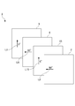
- FIG. 1 is a cross-sectional view showing a light control film 1 according to an embodiment of the present invention.
- the light control film 1 is mainly used in the form of a light control member that is affixed to a transparent member such as glass or a transparent resin substrate or is sandwiched between laminated glasses (transparent members). More specifically, the light control film 1 is a part that performs light control such as a window glass of a building, a showcase, an indoor transparent partition, or a part that receives external light from a vehicle (for example, a front window, a side window, etc. , A rear window, a roof window, a sun visor, etc.) by being attached with an adhesive layer or the like, and the amount of transmitted light is controlled by changing the applied voltage.
- a vehicle for example, a front window, a side window, etc. , A rear window, a roof window, a sun visor, etc.
- the light control film 1 is a film material that controls transmitted light using liquid crystal, and includes a liquid crystal cell 4 for light control film sandwiched between a first polarizing plate 2 and a second polarizing plate 3.
- the first polarizing plate 2 and the second polarizing plate 3 are impregnated with polyvinyl alcohol (PVA) with iodine or the like and then stretched to form an optical functional layer that performs an optical function as a linear polarizing plate.
- the optical functional layer is sandwiched between transparent film members such as acetylcellulose).
- the first polarizing plate 2 and the second polarizing plate 3 are respectively provided with retardation films 2A and 3A for optical compensation on the liquid crystal cell 4 side, but the retardation films 2A and 3A are omitted as necessary. May be.
- the liquid crystal cell 4 controls the polarization plane of transmitted light by an applied voltage to a transparent electrode described later.
- the light control film 1 is comprised so that transmitted light can be controlled and various light control can be aimed at.
- the liquid crystal cell 4 is configured by sandwiching a liquid crystal layer 8 between a first laminated body 5U and a second laminated body 5D that are in the form of a film.
- the second laminate 5D is formed by producing a transparent electrode layer 11, a spacer 12, and an alignment layer 13 on a transparent film-like substrate 6.
- the first laminated body 5U is formed by laminating a transparent electrode layer 16 and an alignment layer 17 on a transparent film-like substrate 15.
- the liquid crystal cell 4 controls the alignment of the liquid crystal material provided in the liquid crystal layer 8 by the VA (Vertical Alignment) method by driving the transparent electrode layers 11 and 16 provided in the first stacked body 5U and the second stacked body 5D.
- VA Vertical Alignment
- the VA method is a method of controlling the transmitted light by changing the alignment of the liquid crystal between vertical alignment and horizontal alignment.
- the liquid crystal layer 14 is sandwiched between the vertical alignment layers by vertically aligning the liquid crystal.
- a liquid crystal cell 4 is configured and configured to horizontally align the liquid crystal material by applying an electric field.
- normally black is “light-shielded” when the voltage is OFF and “transmitted” when the voltage is ON. It becomes a state.
- normally black or normally white changes depending on whether parallel Nicol or crossed Nicol, it is necessary to change the voltage ON / OFF.
- the so-called normally white state in which “light shielding” is performed when the voltage is turned on and light is “transmitted” when the voltage is turned off. It becomes.
- Normally black is a structure in which the transmittance is minimized when a voltage is not applied to the liquid crystal, resulting in a black screen.
- Normally white is a structure in which the transmittance is maximized and transparent when no voltage is applied to the liquid crystal.
- Various transparent film materials applicable to this kind of film material can be applied to the base materials 6 and 15, but a film material having a small optical anisotropy and an in-plane retardation of 10 nm or less is applied. It is preferable.
- a polycarbonate film is applied to the substrates 6 and 15, but a COP (cycloolefin polymer) film or the like may be applied.
- the transparent electrode layers 11 and 16 are formed of a transparent electrode material made of ITO (Indium Tin Oxide).
- the spacer 12 is provided to define the thickness of the liquid crystal layer 8 and various resin materials can be widely applied.
- the spacer 12 is made of a photoresist, and the substrate on which the transparent electrode layer 11 is made. It is produced by applying a photoresist on 6 and exposing and developing.
- the spacer 12 may be provided in the first stacked body 5U, or may be provided in both the first stacked body 5U and the second stacked body 5D.
- the alignment layers 13 and 17 are produced by rubbing the incident polyimide resin layer.
- the alignment layers 13 and 17 can be applied with various configurations capable of expressing the alignment regulating force with respect to the liquid crystal material related to the liquid crystal layer 8, and may be formed by a so-called photo-alignment layer. You may form and form the fine line-shaped uneven
- the spacer 12 may be provided on the alignment layer 13.
- the photo-alignment material various materials to which a photo-alignment technique can be applied can be applied. However, in this embodiment, after the alignment, the alignment does not change due to ultraviolet irradiation, for example, a photodimerization type. Use materials. As for this photodimerization type material, “M. Schadt, K. Schmitt, V. Kozinkov and V. Chigrinov: Jpn. J. Appl. Phys., 31, 2155 (1992)”, “M. Seiberle and A. Schuster: Nature, 381, 212 (1996).
- liquid crystal materials applicable to this kind of light control film can be widely applied to the liquid crystal layer 8.
- a sealing material 19 is disposed so as to surround the liquid crystal layer 8, and the first stacked body 5 ⁇ / b> U and the second stacked body 5 ⁇ / b> D are integrally held by the sealing material 19, and leakage of the liquid crystal material is prevented.
- FIG. 2 is a view for explaining the arrangement of the base materials 6 and 15 in the light control film 1.
- the base materials 6 and 15 are manufactured from the same material. Even if the base material 6 and the base material 15 are made of the same film material, there is a variation, so that they differ from each other by about ⁇ 10 ⁇ m. However, the thickness of the substrate 6 is more preferably ⁇ 5 ⁇ m.
- the optical anisotropy of the substrates 6 and 15 is sufficiently small, and specifically, the in-plane retardation is preferably 10 nm or less.
- a polycarbonate film or the like is applied to the substrates 6 and 15, and this polycarbonate film has an in-plane retardation of as small as 10 nm or less.
- the transmittance at the time of light shielding may increase and may not be ignored.
- the slow axis of the substrate on which the polarized light is incident is not parallel or perpendicular to the polarized light
- the light incident on the substrate has a slow axis component and a fast axis component. It will be. Then, the incident light becomes elliptically polarized light and enters the liquid crystal layer 8 due to the optical anisotropy of the substrate 6.
- the vibration direction of light incident on the substrate 6, that is, the transmission axis (polarization axis) of the second polarizing plate 3 and the main axis (slow axis or fast axis) of the substrate 6 are parallel. It arrange
- FIG. 2 is a diagram showing the relationship between the slow axes L6 and L15 of the substrates 6 and 15 and the transmission axes L2 and L3 of the first polarizing plate 2 and the second polarizing plate 3.
- the 1st polarizing plate 2 and the 2nd polarizing plate 3 are arrange
- the 1st polarizing plate 2 and the 2nd polarizing plate 3 may be crossed Nicol arrangement.
- the slow axis L6 of the substrate 6 is arranged so as to be parallel to the transmission axis L3 of the second polarizing plate 3.
- the slow axis L15 of the substrate 15 is arranged so as to be parallel to the transmission axis L2 of the first polarizing plate 2. That is, the fast axis of the substrate 6 is arranged so as to be orthogonal to the transmission axis L3 of the second polarizing plate 3. The fast axis of the substrate 15 is arranged so as to be orthogonal to the transmission axis L2 of the first polarizing plate 2.
- the present invention is not limited to this, and the slow axis L6 of the substrate 6 may be arranged so as to be orthogonal to the transmission axis L3 of the second polarizing plate 3.
- the slow axis L15 of the substrate 15 may be arranged so as to be orthogonal to the transmission axis L2 of the first polarizing plate 2. That is, the fast axis of the base material 6 is arranged to be parallel to the transmission axis L3 of the second polarizing plate 3, and the fast axis of the base material 15 is set to the transmission axis L2 of the first polarizing plate 2. You may arrange
- the direction in which the main axis of the substrate 6 extends and the direction in which the transmission axis L3 of the second polarizing plate 3 extends may be in parallel or orthogonal to each other. Further, the direction in which the main axis of the substrate 15 extends and the direction in which the transmission axis L2 of the first polarizing plate 2 extends may be in parallel or orthogonal to each other.
- the range perpendicular to the principal axes of the substrates 6 and 15 and the transmission axes of the first polarizing plate 2 and the second polarizing plate 3 is within 90 ° ⁇ 5 ° including measurement errors and manufacturing errors. However, from the viewpoint of sufficiently suppressing the transmittance at the time of light shielding, it is preferably within 90 ° ⁇ 2 °, and more preferably within 90 ° ⁇ 1 °.
- the parallel range of the main axes of the substrates 6 and 15 and the transmission axes of the first polarizing plate 2 and the second polarizing plate 3 is within an angle of 0 ° ⁇ 5 ° including measurement errors and manufacturing errors. However, from the viewpoint of sufficiently suppressing the transmittance at the time of light shielding, it is preferably within 0 ° ⁇ 2 °, and more preferably within 0 ° ⁇ 1 °.
- FIG. 3 is a flowchart showing the manufacturing process of the light control film 1.
- transparent electrode layers 11 and 16 are respectively formed on the substrates 6 and 15 by applying a photolithography technique in the electrode manufacturing process SP2.
- a photoresist film is prepared on the substrate 6, and then exposed and developed, whereby the spacer 12 is prepared.
- a polyimide resin layer is applied on the base material 6 formed of the spacer 12 and on the base material 15 formed of the transparent electrode layer 16. After coating the liquid, it is dried and heat-treated, thereby producing a polyimide film.
- the polyimide film is rubbed to produce the alignment layers 13 and 17.
- a sealant is applied in a frame shape using a dispenser to the base material 6 formed with the alignment layer 13, and then a predetermined position surrounded by the frame shape.
- the liquid crystal material according to the liquid crystal layer 8 is dropped using a dispenser.
- the base materials 6 and 15 are stacked, the first stacked body 5U and the second stacked body 5D are sealed with the sealing material 19 so that the liquid crystal layer 8 is sandwiched by pressing and heating.
- the light control film 1 is produced by laminating and integrating.
- the light that has passed through the second polarizing plate 3 becomes polarized light in the direction of the transmission axis L3 of the second polarizing plate 3.
- the light incident on the substrate 6 is polarized light in the direction of the transmission axis L3 parallel to the slow axis L6 of the substrate 6. That is, the light incident on the substrate 6 includes only the slow axis L6 component and does not include the fast axis component. Therefore, the polarized light incident on the base material 6 is emitted from the base material 6 as linearly polarized light and enters the liquid crystal layer 8. That is, it does not exit from the substrate 6 as elliptically polarized light.
- the relationship between the main axis of the base material 15 (slow axis L15 in the embodiment) and the transmission axis L2 of the first polarizing plate 2 is the same as that of the main axis of the base material 6 (slow axis L6 in the embodiment) and the second polarizing plate 3. This is the same as the relationship with the transmission axis L3.
- the transmitted light including the transmission axis direction component of the output-side linear polarizing plate is not emitted from the liquid crystal layer 8 at the time of light shielding.
- the transmittance can be reduced.
- permeability it is what is called a black transmittance
- the light control film 1 can light-shield the transmitted light more reliably compared with the past.
- Example 1-10 shown in Table 1 below where the relationship between the arrangement of the first polarizing plate 2 and the second polarizing plate 3 and the base materials 6 and 15 is transmitted light actually transmitted through the light control film 1 An experiment was conducted to confirm the light shielding state.
- Example 1-5 is the case where the substrates 6 and 15 are polycarbonate film materials
- Example 6-10 is the case where the substrates 6 and 15 are COP film materials.
- each angle of the slow axis of the substrate 6, the slow axis of the substrate 15, and the transmission axis of the second polarizing plate 3 is an azimuth angle with respect to the transmission axis 0 ° of the first polarizing plate 2. is there.
- the transmittance of the polarizing plates of each of Examples and Comparative Examples described below can be measured by a known spectroscopic technique. For example, RETS-100 (manufactured by Otsuka Electronics Co., Ltd.), KOBRA- It can be measured using WR (manufactured by Oji Scientific Instruments) or the like.
- the slow axis (fast axis) of the base materials 6 and 15 can be obtained by measuring the in-plane retardation of the base material and measuring the orientation angle by a spectroscopic technique. Specifically, a base material is arranged between two polarizing plates arranged in crossed Nicols, and the base material is rotated around the normal direction, and the one polarized light that has the lowest transmittance through the polarizing plate. The direction corresponding to the transmission axis of the plate is the slow axis of the substrate.
- the transmittance can be measured by a known spectroscopic method, for example, using RETS-100 (manufactured by Otsuka Electronics Co., Ltd.) or KOBRA-WR (manufactured by Oji Scientific Instruments Co., Ltd.). Can be measured.
- a transparent electrode or an alignment layer may be formed on each substrate as described above. However, since the alignment layer has no retardation, it is provided on the substrate. The above measurement does not affect the measurement result.
- the transparent electrode may have a phase difference, when measuring in a state where the transparent electrode is provided on the substrate, the retardation Re of the transparent electrode is preferably Re ⁇ 10 nm, and Re ⁇ More desirably, it is 5 nm.
- the linear polarizing plate and the base material are bonded with the adhesive, the linear polarizing plate is peeled off from the base material, and the adhesive on the base material is removed with ethyl acetate or the like, so that the fast axis of the base material The direction of the slow axis can be accurately measured.
- a polycarbonate film material having a thickness of 100 ⁇ m with hard coat layers formed on both surfaces was applied to the base materials 6 and 15, and the light control film 1 was manufactured according to the configuration of the above-described embodiment.
- the retardation films 2A and 3A are omitted.
- the arrangement of the substrates 6 and 15, the first polarizing plate 2 and the second polarizing plate 3 is the arrangement shown in Example 1 in Table 1 and is the same as that in FIG. In Example 1, the transmittance was 0.1% when a voltage was applied, and it was confirmed that the transmitted light could be sufficiently shielded when the light was shielded.
- Example 2 In the same manner as in Example 1, a polycarbonate film material having a thickness of 100 ⁇ m with hard coat layers formed on both sides was applied to the base materials 6 and 15, and the light control film 1 was manufactured with the configuration of the above-described embodiment.
- the retardation films 2A and 3A are omitted.
- the arrangement of the substrates 6 and 15, the first polarizing plate 2 and the second polarizing plate 3 is the arrangement shown in Example 2 in Table 1, and is shown in FIG.
- the transmittance was 0.1% when a voltage was applied, and it was confirmed that the transmitted light could be sufficiently shielded when the light was shielded.
- Example 3 In the same manner as in Example 1, a polycarbonate film material having a thickness of 100 ⁇ m with hard coat layers formed on both sides was applied to the base materials 6 and 15, and the light control film 1 was manufactured with the configuration of the above-described embodiment.
- the retardation films 2A and 3A are omitted.
- the arrangement of the substrates 6 and 15, the first polarizing plate 2 and the second polarizing plate 3 is the arrangement shown in Example 3 in Table 1, and is shown in FIG.
- the transmittance was 0.2% when there was no electric field, and it was confirmed that the transmitted light could be sufficiently shielded when shielded.
- Example 4 In the same manner as in Example 1, a polycarbonate film material having a thickness of 100 ⁇ m with hard coat layers formed on both sides was applied to the base materials 6 and 15, and the light control film 1 was manufactured with the configuration of the above-described embodiment.
- the retardation films 2A and 3A are omitted.
- the arrangement of the substrates 6 and 15, the first polarizing plate 2 and the second polarizing plate 3 is the arrangement shown in Example 4 in Table 1, and is shown in FIG.
- the transmittance was 0.1% when there was no electric field, and it was confirmed that the transmitted light could be sufficiently shielded when shielded.
- Example 5 In the same manner as in Example 1, a polycarbonate film material having a thickness of 100 ⁇ m with hard coat layers formed on both sides was applied to the base materials 6 and 15, and the light control film 1 was manufactured with the configuration of the above-described embodiment.
- the retardation films 2A and 3A are omitted.
- the arrangement of the substrates 6 and 15, the first polarizing plate 2 and the second polarizing plate 3 is the arrangement shown in Example 5 of Table 1 and is illustrated in FIG.
- the transmittance was 0.2% when there was no electric field, and it was confirmed that the transmitted light could be sufficiently shielded when shielded.
- a COP film material having a thickness of 100 ⁇ m with hard coat layers prepared on both sides was applied to the base materials 6 and 15, and the light control film 1 was prepared according to the configuration of the above-described embodiment.
- the retardation films 2A and 3A are omitted.
- the arrangement of the substrates 6 and 15, the first polarizing plate 2, and the second polarizing plate 3 is the arrangement shown in Example 6 in Table 1 and is the same as FIG.
- the transmittance was 0.1% when there was no electric field, and it was confirmed that the transmitted light could be sufficiently shielded when a voltage was applied.
- Example 7 In the same manner as in Example 6, a COP film material having a thickness of 100 ⁇ m with hard coat layers formed on both sides was applied to the base materials 6 and 15, and the light control film 1 was manufactured with the configuration of the above-described embodiment.
- the retardation films 2A and 3A are omitted.
- the arrangement of the substrates 6 and 15, the first polarizing plate 2, and the second polarizing plate 3 is the arrangement shown in Example 7 in Table 1 and is the same as that in FIG. 4.
- the transmittance was 0.1% when a voltage was applied, and it was confirmed that the transmitted light could be sufficiently shielded when the light was shielded.
- Example 8 a COP film material having a thickness of 100 ⁇ m with hard coat layers formed on both sides was applied to the base materials 6 and 15, and the light control film 1 was manufactured with the configuration of the above-described embodiment.
- the retardation films 2A and 3A are omitted.
- the arrangement of the substrates 6 and 15, the first polarizing plate 2 and the second polarizing plate 3 is the arrangement shown in Example 8 of Table 1 and is the same as FIG.
- the transmittance was 0.2% when there was no electric field, and it was confirmed that the transmitted light could be sufficiently shielded when shielded.
- Example 9 In the same manner as in Example 6, a COP film material having a thickness of 100 ⁇ m with hard coat layers formed on both sides was applied to the base materials 6 and 15, and the light control film 1 was manufactured with the configuration of the above-described embodiment.
- the retardation films 2A and 3A are omitted.
- the arrangement of the substrates 6 and 15, the first polarizing plate 2, and the second polarizing plate 3 is the same as that shown in FIG.
- the transmittance was 0.1% when there was no electric field, and it was confirmed that the transmitted light could be sufficiently shielded when shielded.
- Example 10 In the same manner as in Example 6, a COP film material having a thickness of 100 ⁇ m with hard coat layers formed on both sides was applied to the base materials 6 and 15, and the light control film 1 was manufactured with the configuration of the above-described embodiment.
- the retardation films 2A and 3A are omitted.
- the arrangement of the substrates 6 and 15, the first polarizing plate 2 and the second polarizing plate 3 is the arrangement shown in Example 10 and is illustrated in FIG.
- the transmittance was 0.2% when there was no electric field, and it was confirmed that the transmitted light could be sufficiently shielded when shielded.
- Comparative Example 1 A PET film material having a thickness of 100 ⁇ m with hard coat layers prepared on both sides was applied to the base materials 6 and 15, and a light control film was prepared according to the configuration of the above-described embodiment.
- the retardation films 2A and 3A are omitted.
- the arrangement of the base materials 6 and 15, the first polarizing plate 2 and the second polarizing plate 3 is the same as in FIG.
- the transmittance was 10% when there was no electric field, and when the light was shielded, the light-shielding efficiency of transmitted light was reduced compared to the above-described embodiment.
- Comparative Example 2 A COP film material having a thickness of 100 ⁇ m with hard coat layers formed on both surfaces was applied to the substrates 6 and 15, and the light control film 1 was manufactured with the same configuration as that of the above-described embodiment.
- the retardation films 2A and 3A are omitted.
- the slow axis of the substrate 15 is inclined by 10 ° with respect to the transmission axis of the first polarizing plate 2.
- the slow axis of the substrate 6 is inclined by 10 ° with respect to the transmission axis of the second polarizing plate 3.
- the transmittance was 5% when a voltage was applied, and when the light was shielded, the light-shielding efficiency of transmitted light was reduced compared to the above-described embodiment.
- the liquid crystal material is driven by the VA method.
- the slow axis of the first base material 15 and the transmission axis of the first polarizing plate 2 are parallel or orthogonal to each other, and the slow axis of the second base material 6 and the transmission of the second polarizing plate 3.
- the axes are in parallel or orthogonal to each other, the most effective light shielding efficiency is obtained at the time of light shielding.
- the present invention is not limited to this, and the TN (Twisted Nematic) system, IPS (In-Plane-Switching) system A driving method such as the above may be applied.
- nematic liquid crystal is arranged in the liquid crystal layer 8 between the two first polarizing plates 2 and the second polarizing plate 3 that face each other while being shifted by 90 degrees.
- the orientation layers 17 and 13 make the orientation of the liquid crystal molecules coincide with the orientations of the first polarizing plate 2 and the second polarizing plate 3 on the orientation layers 17 and 13 side.
- a driving electrode is collectively produced on one of a pair of substrates sandwiching a liquid crystal layer, and a so-called transverse electric field which is an electric field in the in-plane direction of the substrate surface is formed by this electrode.
- This is a driving method for controlling the alignment of the liquid crystal by forming the.
- the spacer is manufactured using the photoresist.
- the present invention is not limited to this, and a so-called bead spacer may be applied.
Landscapes
- Physics & Mathematics (AREA)
- Nonlinear Science (AREA)
- Optics & Photonics (AREA)
- General Physics & Mathematics (AREA)
- Crystallography & Structural Chemistry (AREA)
- Chemical & Material Sciences (AREA)
- Liquid Crystal (AREA)
- Mathematical Physics (AREA)
- Engineering & Computer Science (AREA)
- Structural Engineering (AREA)
- Architecture (AREA)
- Civil Engineering (AREA)
- Polarising Elements (AREA)
Abstract
従来に比して一段と確実に透過光を遮光することができる調光フィルム、調光部材、車両を提供する。 本発明の調光フィルム1は、液晶層8と、前記液晶層8の少なくとも一方の側に配置された透明電極層15,11と、前記液晶層8及び前記透明電極層16の第1の側に配置された第1基材15と、前記第1基材15の前記第1の側に配置された第1偏光板2と、前記液晶層8及び前記透明電極層11の第2の側に配置された第2基材6と、前記第2基材6の前記第2の側に配置された第2偏光板3と、を備え、前記第1基材15の遅相軸と前記第1偏光板2の透過軸とが、互いに平行又は直交関係にあり、前記第2基材6の遅相軸と前記第2偏光板3の透過軸とが、互いに平行又は直交関係にある。
Description
本発明は、例えば窓に貼り付けて外来光の透過を制御する電子ブラインド等に利用可能な調光フィルム、調光部材、車両に関する。
従来、例えば窓に貼り付けて外来光の透過を制御する調光フィルムに関する工夫が種々に提案されている(特許文献1、2)。このような調光フィルムの1つに、液晶を利用したものがある。液晶を利用した調光フィルムは、透明電極を備える透明フィルム材により液晶材料を挟持して液晶セルが作製され、この液晶セルを直線偏光板により挟持する。そして、液晶に印加する電界を変化させることにより液晶の配向を変化させ、外来光を遮光したり透過したりし、さらには透過光量を変化させ、これらにより外来光の透過を制御する。
この種の調光フィルムでは、遮光時における透過率を低減して、従来に比して一段と確実に透過光を遮光できるようにすることが望まれている。
本発明はこのような状況に鑑みてなされたものであり、調光フィルムに関して、従来に比して一段と確実に透過光を遮光できるようにすることを目的とする。
本発明者は、上記課題を解決するために鋭意研究を重ね、偏光板の透過軸と、基材における複屈折の主軸(遅相軸及び進相軸)とを、互いに直交又は平行にすることにより、遮光時おける透過率を低減する、との着想に至り、本発明を完成するに至った。なお、遅相軸は、屈折率異方性を有する材料における屈折率が最大となる方向である。なお、進相軸は、屈折率異方性を有する材料における屈折率が最小となる方向である。
具体的には、本発明では、以下のようなものを提供する。
(1)液晶層と、前記液晶層の少なくとも一方の側に配置された透明電極層と、前記液晶層及び前記透明電極層の第1の側に配置された第1基材と、前記第1基材の前記第1の側に配置された第1偏光板と、前記液晶層及び前記透明電極層の第2の側に配置された第2基材と、前記第2基材の前記第2の側に配置された第2偏光板と、を備え、前記第1基材の遅相軸と前記第1偏光板の透過軸とが、互いに平行又は直交関係にあり、前記第2基材の遅相軸と前記第2偏光板の透過軸とが、互いに平行又は直交関係にある、調光フィルム。
(1)液晶層と、前記液晶層の少なくとも一方の側に配置された透明電極層と、前記液晶層及び前記透明電極層の第1の側に配置された第1基材と、前記第1基材の前記第1の側に配置された第1偏光板と、前記液晶層及び前記透明電極層の第2の側に配置された第2基材と、前記第2基材の前記第2の側に配置された第2偏光板と、を備え、前記第1基材の遅相軸と前記第1偏光板の透過軸とが、互いに平行又は直交関係にあり、前記第2基材の遅相軸と前記第2偏光板の透過軸とが、互いに平行又は直交関係にある、調光フィルム。
(2) (1)において、前記第1偏光板の透過軸と、前記第2偏光板の透過軸とが、互いに平行又は直交関係にある、調光フィルム。
(3) (1)または(2)において、前記第1基材及び前記第2基材が、ポリカーボネートフィルム、シクロオレフィンポリマーフィルムの何れかである、調光フィルム。
(4) (1)から(3)のいずれかにおいて、前記第1基材及び前記第2基材の面内位相差が10nm以下である、調光フィルム。
(5) 透明部材と、
前記透明部材に配置される(1)から(4)までのいずれかの調光フィルムと、
を備える調光部材。
前記透明部材に配置される(1)から(4)までのいずれかの調光フィルムと、
を備える調光部材。
(6) 外光が入射する部位に配置される(1)から(4)までのいずれかの調光フィルムを備える、
車両。
車両。
本発明によれば、調光フィルムに関して、従来に比して一段と確実に透過光を遮光することができる。
〔調光フィルム〕
図1は、本発明の実施形態に係る調光フィルム1を示す断面図である。調光フィルム1は、ガラスや、透明樹脂基板等の透明部材に貼付されたり、合わせガラス(透明部材)に挟持されたりした調光部材の形態で主に使用される。より具体的には、調光フィルム1は、建築物の窓ガラス、ショーケース、屋内の透明パーテーション等の調光を図る部位や、車両の外光が入射する部位(例えば、フロントウインドウ、サイドウインドウ、リアウインドウ、ルーフウインドウ、サンバイザー等)に、粘着剤層等により貼り付けて使用され、印加電圧を変化させることにより、透過光の光量が制御される。
図1は、本発明の実施形態に係る調光フィルム1を示す断面図である。調光フィルム1は、ガラスや、透明樹脂基板等の透明部材に貼付されたり、合わせガラス(透明部材)に挟持されたりした調光部材の形態で主に使用される。より具体的には、調光フィルム1は、建築物の窓ガラス、ショーケース、屋内の透明パーテーション等の調光を図る部位や、車両の外光が入射する部位(例えば、フロントウインドウ、サイドウインドウ、リアウインドウ、ルーフウインドウ、サンバイザー等)に、粘着剤層等により貼り付けて使用され、印加電圧を変化させることにより、透過光の光量が制御される。
調光フィルム1は、液晶を利用して透過光を制御するフィルム材あり、第1偏光板2及び第2偏光板3により調光フィルム用の液晶セル4を挟持して構成される。
〔直線偏光板〕
第1偏光板2及び第2偏光板3は、ポリビニルアルコール(PVA)にヨウ素等を含浸させた後、延伸して直線偏光板としての光学的機能を果たす光学機能層が形成され、TAC(トリアセチルセルロース)等の透明なフィルム部材により光学機能層を挟持して作製される。第1偏光板2及び第2偏光板3には、それぞれ液晶セル4側に光学補償を行うための位相差フィルム2A、3Aが設けられるが、位相差フィルム2A、3Aは、必要に応じて省略してもよい。
第1偏光板2及び第2偏光板3は、ポリビニルアルコール(PVA)にヨウ素等を含浸させた後、延伸して直線偏光板としての光学的機能を果たす光学機能層が形成され、TAC(トリアセチルセルロース)等の透明なフィルム部材により光学機能層を挟持して作製される。第1偏光板2及び第2偏光板3には、それぞれ液晶セル4側に光学補償を行うための位相差フィルム2A、3Aが設けられるが、位相差フィルム2A、3Aは、必要に応じて省略してもよい。
液晶セル4は、後述する透明電極への印加電圧により透過光の偏光面を制御する。これにより調光フィルム1は、透過光を制御して種々に調光を図ることができるように構成される。
〔液晶セル〕
液晶セル4は、フィルム形状である第1積層体5U及び第2積層体5Dにより、液晶層8を挟持して構成される。第2積層体5Dは、透明なフィルム状の基材6に、透明電極層11、スペーサ12、配向層13を作製して形成される。第1積層体5Uは、透明なフィルム状の基材15に、透明電極層16、配向層17を積層して形成される。液晶セル4は、第1積層体5U及び第2積層体5Dに設けられた透明電極層11、16の駆動により、VA(Vertical Alignment)方式により液晶層8に設けられた液晶材料の配向を制御し、これにより透過光の偏光面を制御する。
VA方式は、液晶の配向を垂直配向と水平配向とで変化させて透過光を制御する方式であり、無電界時、液晶を垂直配向させることにより、液晶層14を垂直配向層により挟持して液晶セル4が構成され、電界の印加により液晶材料を水平配向させるように構成される。
VA方式では、第1偏光板2と第2偏光板3とがクロスニコルに配置されている場合、電圧OFF時に「遮光」され、電圧ON時に光が「透過」となる、いわゆるノーマリーブラックの状態となる。
また、パラレルニコルかクロスニコルかによって、ノーマリーブラックかノーマリーホワイトかが変わるので電圧のON/OFFを変える必要がある。このため、第1偏光板2と第2偏光板3とがパラレルニコルに配置されている場合、電圧ON時に「遮光」され、電圧OFF時に光が「透過」となる、いわゆるノーマリーホワイトの状態となる。
ノーマリーブラックとは、液晶に電圧がかかっていない時に透過率が最小となり、黒い画面になる構造である。ノーマリーホワイトとは、液晶に電圧がかかっていない時に透過率が最大となり、透明となる構造である。
基材6、15は、この種のフィルム材に適用可能な種々の透明フィルム材を適用することができるが、光学異方性が小さく、面内位相差が10nm以下であるフィルム材を適用することが好ましい。実施形態において、基材6、15は、ポリカーボネートフィルムが適用されるが、COP(シクロオレフィンポリマー)フィルム等を適用してもよい。
透明電極層11、16は、この種のフィルム材に適用される各種の電極材料を適用することができ、本実施形態ではITO(Indium Tin Oxide)による透明電極材により形成される。スペーサ12は、液晶層8の厚みを規定するために設けられ、各種の樹脂材料を広く適用することができるが、本実施形態ではフォトレジストにより作製され、透明電極層11が作製された基材6の上に、フォトレジストを塗工して露光、現像することにより作製される。なおスペーサ12は、第1積層体5Uに設けるようにしてもよく、第1積層体5U及び第2積層体5Dの双方に設けるようにしてもよい。
配向層13、17は入射する、ポリイミド樹脂層をラビング処理して作製される。なお配向層13、17は、液晶層8に係る液晶材料に対して配向規制力を発現可能な各種の構成を適用することができ、いわゆる光配向層により作製してもよく、ラビング処理、研磨処理による微細なライン状凹凸形状を賦型処理により作製して形成してもよい。なおスペーサ12は、配向層13の上に設けるようにしてもよい。
なお光配向材料は、光配向の手法を適用可能な各種の材料を適用することができるが、本実施形態では、一旦配向した後には、紫外線の照射によって配向が変化しない、例えば光二量化型の材料を使用する。この光二量化型の材料については、「M.Schadt, K.Schmitt, V. Kozinkov and V. Chigrinov : Jpn. J. Appl.Phys., 31, 2155 (1992)」、「M. Schadt, H. Seiberle and A. Schuster : Nature, 381, 212(1996)」等に開示されている。
液晶層8は、この種の調光フィルムに適用可能な各種の液晶材料を広く適用することができる。なお液晶セル4は、液晶層8を囲むように、シール材19が配置され、このシール材19により第1積層体5U、第2積層体5Dが一体に保持され、液晶材料の漏出が防止される。
〔基材〕
図2は、調光フィルム1における基材6、15の配置を説明する図である。基材6、15は、互いに同一の材料で製造されている。基材6と基材15とを、同一のフィルム材で製造した場合であっても、バラツキがあるため、互いに±10μm程度異なる。ただし、基材6の厚み±5μmが基材15の厚みであることがより好ましい。
図2は、調光フィルム1における基材6、15の配置を説明する図である。基材6、15は、互いに同一の材料で製造されている。基材6と基材15とを、同一のフィルム材で製造した場合であっても、バラツキがあるため、互いに±10μm程度異なる。ただし、基材6の厚み±5μmが基材15の厚みであることがより好ましい。
基材6、15の光学異方性は十分に小さく、具体的には面内位相差は10nm以下が好ましい。基材6、15にはポリカーボネートフィルム等が適用され、このポリカーボネートフィルムは面内位相差が10nm以下と極めて小さいものである。
しかし、種々に実験した結果によれば、このように面内位相差が10nm以下の透明フィルム材であっても、遮光時の透過率が増大し、無視し得ない場合があることが判った。例えば、偏光された光が入射する基材の遅相軸が、その偏光に対して平行又は垂直でない場合、基材に入射する光は、遅相軸成分と進相軸成分とを備えていることになる。そうすると、基材6の光学異方性により入射光は楕円偏光となって液晶層8に入射する。その結果、何ら透明電極層11、16に電圧を印加していない状態で(液晶層8への無電界時)、出射側直線偏光板の透過軸方向成分を含む透過光が液晶層8から出射されることになり、これにより充分に透過率を低減できなくなる。
〔偏光板及び基材の配置〕
そこで、本実施形態では、基材6に入射する光の振動方向、すなわち第2偏光板3の透過軸(偏光軸)と、基材6の主軸(遅相軸又は進相軸)とが平行となるように、または直交するように配置する。また、基材15に入射する光の振動方向、すなわち第1偏光板2の透過軸(偏光軸)と、基材15の主軸(遅相軸又は進相軸)とが平行となるように、または直交するように配置する。
そこで、本実施形態では、基材6に入射する光の振動方向、すなわち第2偏光板3の透過軸(偏光軸)と、基材6の主軸(遅相軸又は進相軸)とが平行となるように、または直交するように配置する。また、基材15に入射する光の振動方向、すなわち第1偏光板2の透過軸(偏光軸)と、基材15の主軸(遅相軸又は進相軸)とが平行となるように、または直交するように配置する。
図2は、基材6,15の遅相軸L6,L15と、第1偏光板2及び第2偏光板3の透過軸L2,L3との配置の関係を示した図である。図2において、第1偏光板2及び第2偏光板3はパラレルニコル配置で紫外線硬化性樹脂等による接着剤層により液晶セル4に配置されている。ただし、これに限定されず、第1偏光板2及び第2偏光板3はクロスニコル配置であってもよい。
基材6の遅相軸L6は、第2偏光板3の透過軸L3に対して平行となるように配置されている。基材15の遅相軸L15は、第1偏光板2の透過軸L2に対して平行となるように配置されている。
すなわち、基材6の進相軸は、第2偏光板3の透過軸L3に対して直交するように配置されている。基材15の進相軸は、第1偏光板2の透過軸L2に対して直交するように配置されている。
基材6の遅相軸L6は、第2偏光板3の透過軸L3に対して平行となるように配置されている。基材15の遅相軸L15は、第1偏光板2の透過軸L2に対して平行となるように配置されている。
すなわち、基材6の進相軸は、第2偏光板3の透過軸L3に対して直交するように配置されている。基材15の進相軸は、第1偏光板2の透過軸L2に対して直交するように配置されている。
ただし、これに限定されず、基材6の遅相軸L6は、第2偏光板3の透過軸L3に対して直交するように配置されていてもよい。基材15の遅相軸L15は、第1偏光板2の透過軸L2に対して直交するように配置されていてもよい。
すなわち、基材6の進相軸は、第2偏光板3の透過軸L3に対して平行となるように配置され、基材15の進相軸は、第1偏光板2の透過軸L2に対して平行となるように配置されていてもよい。
すなわち、基材6の進相軸は、第2偏光板3の透過軸L3に対して平行となるように配置され、基材15の進相軸は、第1偏光板2の透過軸L2に対して平行となるように配置されていてもよい。
さらに換言すると、基材6の主軸の延びる方向と、第2偏光板3の透過軸L3の延びる方向とは、互いに平行又は直交関係にあればよい。また、基材15の主軸の延びる方向と、第1偏光板2の透過軸L2の延びる方向とは、互いに平行又は直交関係にあればよい。
なお、基材6,15の主軸と、第1偏光板2及び第2偏光板3の透過軸との直交の範囲は、計測誤差、製造誤差等をも含めて角度が90度±5度以内であるが、遮光時における透過率を実用上充分に抑圧する観点からは、90度±2度以内であることが好ましく、90度±1度以内であることがより好ましい。
また、基材6,15の主軸と、第1偏光板2及び第2偏光板3の透過軸との平行の範囲は、計測誤差、製造誤差等をも含めて角度が0度±5度以内であるが、遮光時における透過率を実用上充分に抑圧する観点からは、0度±2度以内であることが好ましく、0度±1度以内であることがより好ましい。
また、基材6,15の主軸と、第1偏光板2及び第2偏光板3の透過軸との平行の範囲は、計測誤差、製造誤差等をも含めて角度が0度±5度以内であるが、遮光時における透過率を実用上充分に抑圧する観点からは、0度±2度以内であることが好ましく、0度±1度以内であることがより好ましい。
〔製造工程〕
図3は、調光フィルム1の製造工程を示すフローチャートである。この製造工程は、電極作製工程SP2おいて、フォトリソグラフィーの手法を適用して、基材6、15の上に透明電極層11、16をそれぞれ作成する。
さらに続いてスペーサ作製工程SP3において、基材6にフォトレジスト膜を作製した後、露光、現像処理し、これによりスペーサ12を作製する。
続いて製造工程は、配向層作製工程SP4において、スペーサ12を作製してなる基材6の上に、また透明電極層16を作製してなる基材15の上に、ポリイミド樹脂層の塗工液を塗工した後、乾燥、加熱処理し、これによりポリイミド膜を作製する。またこのポリイミド膜をラビング処理し、これにより配向層13、17を作製する。
続いて、この製造工程は、封止工程SP5において、配向層13を作製してなる基材6に、ディスペンサーを使用して枠形状によりシール材を塗布した後、この枠形状により囲まれる所定位置に、ディスペンサーを使用して液晶層8に係る液晶材料を滴下する。
その後、この製造工程は、基材6、15を積層した後、押圧して加熱し、これにより液晶層8を挟持するようにして、第1積層体5U及び第2積層体5Dをシール材19により貼り合せて一体化し、調光フィルム1を作製する。
その後、この製造工程は、基材6、15を積層した後、押圧して加熱し、これにより液晶層8を挟持するようにして、第1積層体5U及び第2積層体5Dをシール材19により貼り合せて一体化し、調光フィルム1を作製する。
本実施形態の調光フィルム1によると、第2偏光板3を通過した光は、第2偏光板3の透過軸L3方向の偏光となる。
基材6に入射する光は、基材6の遅相軸L6と平行な透過軸L3方向の偏光である。すなわち、基材6に入射する光は、遅相軸L6成分のみ備え、進相軸成分を備えていない。したがって、基材6に入射した偏光光は、直線偏光のまま基材6より出射して液晶層8に入射する。すなわち、基材6より楕円偏光となって出射することはない。
基材6に入射する光は、基材6の遅相軸L6と平行な透過軸L3方向の偏光である。すなわち、基材6に入射する光は、遅相軸L6成分のみ備え、進相軸成分を備えていない。したがって、基材6に入射した偏光光は、直線偏光のまま基材6より出射して液晶層8に入射する。すなわち、基材6より楕円偏光となって出射することはない。
基材15の主軸(実施形態では遅相軸L15)と第1偏光板2の透過軸L2との関係も、基材6の主軸(実施形態では遅相軸L6)と第2偏光板3の透過軸L3との関係と同様である。
すなわち、液晶層8に入射する光は、楕円偏光になることがないので、遮光時において出射側直線偏光板の透過軸方向成分を含む透過光が液晶層8から出射されることがなく、充分に透過率を低減できる。
このように、調光フィルム1では、遮光時における透過率(いわゆる黒透過率である)を低減する。これにより調光フィルム1は、従来に比して一段と確実に透過光を遮光することができる。
このように、調光フィルム1では、遮光時における透過率(いわゆる黒透過率である)を低減する。これにより調光フィルム1は、従来に比して一段と確実に透過光を遮光することができる。
次に、上述の実施形態に基づいて製造された調光フィルム1の種々の実施例について説明する。なお、実施形態はVA方式で行った。
第1偏光板2及び第2偏光板3と基材6,15との配置の関係が、以下の表1に示す実施例1-10の場合において、実際に調光フィルム1を透過した透過光の遮光状態を確認する実験を行った。実施例1-5は、基材6、15がポリカーボネートフィルム材の場合、実施例6-10は、基材6、15がCOPフィルム材の場合である。
表1中の基材6の遅相軸、基材15の遅相軸、第2偏光板3の透過軸の各角度は、第1偏光板2の透過軸0°を基準とした方位角である。
また、以下に説明する各実施例、各比較例の偏光板の透過率は、公知の分光学的手法により測定することができ、例えば、RETS-100(大塚電子株式会社製)や、KOBRA-WR(王子計測機器株式会社製)等を用いて測定することができる。
また、基材6、15の遅相軸(進相軸)は、基材の面内位相差の測定と、分光学的手法による配向角の測定とにより求めることができる。具体的には、クロスニコルに配置された2枚の偏光板間に基材を配置し、基材を、法線方向を中心に回転させて、偏光板を通じて最も透過率が低くなる一方の偏光板の透過軸に一致する方向が、基材の遅相軸となる。なお、透過率の測定には、公知の分光学的手法により測定することができ、例えば、RETS-100(大塚電子株式会社製)や、KOBRA-WR(王子計測機器株式会社製)等を用いて測定することができる。
なお、実際には、上述のように各基材上には、透明電極や、配向層が形成されている場合があるが、配向層は位相差を有さないため基材上に設けた状態で上記測定をしても測定結果に影響はない。しかし、透明電極は位相差を有する場合があるため、基材上に透明電極が設けられている状態で測定するときは、透明電極のリタデーションReが、Re<10nmであることが望ましく、Re<5nmであることがより望ましい。
また、粘着剤により直線偏光板と基材が接合されている場合、直線偏光板を基材から剥がして、酢酸エチル等により基材上の粘着剤を除去することにより、基材の進相軸、遅相軸の方向を正確に測定することができる。

なお、実際には、上述のように各基材上には、透明電極や、配向層が形成されている場合があるが、配向層は位相差を有さないため基材上に設けた状態で上記測定をしても測定結果に影響はない。しかし、透明電極は位相差を有する場合があるため、基材上に透明電極が設けられている状態で測定するときは、透明電極のリタデーションReが、Re<10nmであることが望ましく、Re<5nmであることがより望ましい。
また、粘着剤により直線偏光板と基材が接合されている場合、直線偏光板を基材から剥がして、酢酸エチル等により基材上の粘着剤を除去することにより、基材の進相軸、遅相軸の方向を正確に測定することができる。
両面にハードコート層が作製された厚み100μmによるポリカーボネートフィルム材を基材6、15に適用し、上述の実施形態の構成により調光フィルム1を作製した。なお位相差フィルム2A、3Aは省略した。基材6、15、第1偏光板2及び第2偏光板3の配置は表1の実施例1に示す配置で、上述の図2と同様である。実施例1では、電圧印加時、透過率が0.1%であり、遮光時、充分に透過光を遮光できることが確認された。
実施例1と同様に、両面にハードコート層が作製された厚み100μmによるポリカーボネートフィルム材を基材6、15に適用し、上述の実施形態の構成により調光フィルム1を作製した。なお位相差フィルム2A、3Aは省略した。基材6、15、第1偏光板2及び第2偏光板3の配置は表1の実施例2に示す配置で、図4に図示する。実施例2では、電圧印加時、透過率が0.1%であり、遮光時、充分に透過光を遮光できることが確認された。
実施例1と同様に、両面にハードコート層が作製された厚み100μmによるポリカーボネートフィルム材を基材6、15に適用し、上述の実施形態の構成により調光フィルム1を作製した。なお位相差フィルム2A、3Aは省略した。基材6、15、第1偏光板2及び第2偏光板3の配置は表1の実施例3に示す配置で、図5に図示する。実施例3では、無電界時、透過率が0.2%であり、遮光時、充分に透過光を遮光できることが確認された。
実施例1と同様に、両面にハードコート層が作製された厚み100μmによるポリカーボネートフィルム材を基材6、15に適用し、上述の実施形態の構成により調光フィルム1を作製した。なお位相差フィルム2A、3Aは省略した。基材6、15、第1偏光板2及び第2偏光板3の配置は表1の実施例4に示す配置で、図6に図示する。実施例4では、無電界時、透過率が0.1%であり、遮光時、充分に透過光を遮光できることが確認された。
実施例1と同様に、両面にハードコート層が作製された厚み100μmによるポリカーボネートフィルム材を基材6、15に適用し、上述の実施形態の構成により調光フィルム1を作製した。なお位相差フィルム2A、3Aは省略した。基材6、15、第1偏光板2及び第2偏光板3の配置は表1の実施例5に示す配置で、図7に図示する。実施例5では、無電界時、透過率が0.2%であり、遮光時、充分に透過光を遮光できることが確認された。
両面にハードコート層が作製された厚み100μmによるCOPフィルム材を基材6、15に適用し、上述の実施形態の構成により調光フィルム1を作製した。なお位相差フィルム2A、3Aは省略した。基材6、15、第1偏光板2及び第2偏光板3の配置は表1の実施例6に示す配置で、図2と同様である。実施例6では、無電界時、透過率が0.1%であり、電圧印加時、充分に透過光を遮光できることが確認された。
実施例6と同様に、両面にハードコート層が作製された厚み100μmによるCOPフィルム材を基材6、15に適用し、上述の実施形態の構成により調光フィルム1を作製した。なお位相差フィルム2A、3Aは省略した。基材6、15、第1偏光板2及び第2偏光板3の配置は表1の実施例7に示す配置で、図4と同様である。この実施例7では、電圧印加時、透過率が0.1%であり、遮光時、充分に透過光を遮光できることが確認された。
実施例6と同様に、両面にハードコート層が作製された厚み100μmによるCOPフィルム材を基材6、15に適用し、上述の実施形態の構成により調光フィルム1を作製した。なお位相差フィルム2A、3Aは省略した。基材6、15、第1偏光板2及び第2偏光板3の配置は、表1の実施例8に示す配置で、図5と同様である。この実施例8では、無電界時、透過率が0.2%であり、遮光時、充分に透過光を遮光できることが確認された。
実施例6と同様に、両面にハードコート層が作製された厚み100μmによるCOPフィルム材を基材6、15に適用し、上述の実施形態の構成により調光フィルム1を作製した。なお位相差フィルム2A、3Aは省略した。基材6、15、第1偏光板2及び第2偏光板3の配置は、実施例9に示す配置で、図6と同様である。この実施例9では、無電界時、透過率が0.1%であり、遮光時、充分に透過光を遮光できることが確認された。
実施例6と同様に、両面にハードコート層が作製された厚み100μmによるCOPフィルム材を基材6、15に適用し、上述の実施形態の構成により調光フィルム1を作製した。なお位相差フィルム2A、3Aは省略した。基材6、15、第1偏光板2及び第2偏光板3の配置は、実施例10に示す配置で、図7に図示する。この実施例10では、無電界時、透過率が0.2%であり、遮光時、充分に透過光を遮光できることが確認された。
〔比較例1〕
両面にハードコート層が作製された厚み100μmによるPETフィルム材を基材6、15に適用し、上述の実施形態の構成により調光フィルムを作製した。なお位相差フィルム2A、3Aは省略した。基材6、15、第1偏光板2及び第2偏光板3の配置は、図2と同様である。比較例1では、無電界時、透過率が10%であり、遮光時、上述の実施形態と比べると、透過光の遮光効率の低下が見られた。
両面にハードコート層が作製された厚み100μmによるPETフィルム材を基材6、15に適用し、上述の実施形態の構成により調光フィルムを作製した。なお位相差フィルム2A、3Aは省略した。基材6、15、第1偏光板2及び第2偏光板3の配置は、図2と同様である。比較例1では、無電界時、透過率が10%であり、遮光時、上述の実施形態と比べると、透過光の遮光効率の低下が見られた。
〔比較例2〕
両面にハードコート層が作製された厚み100μmによるCOPフィルム材を基材6、15に適用し、上述の実施形態と同様の構成により調光フィルム1を作製した。なお位相差フィルム2A、3Aは省略した。表1の比較例2に示すように、第1偏光板2の透過軸に対して、基材15の遅相軸は10°傾いている。また第2偏光板3の透過軸に対して、基材6の遅相軸は10°傾いている。この比較例2では、電圧印加時、透過率が5%であり、遮光時、上述の実施形態と比べると、透過光の遮光効率の低下が見られた。
両面にハードコート層が作製された厚み100μmによるCOPフィルム材を基材6、15に適用し、上述の実施形態と同様の構成により調光フィルム1を作製した。なお位相差フィルム2A、3Aは省略した。表1の比較例2に示すように、第1偏光板2の透過軸に対して、基材15の遅相軸は10°傾いている。また第2偏光板3の透過軸に対して、基材6の遅相軸は10°傾いている。この比較例2では、電圧印加時、透過率が5%であり、遮光時、上述の実施形態と比べると、透過光の遮光効率の低下が見られた。
〔他の実施形態〕
以上、本発明の実施に好適な具体的な構成を詳述したが、本発明は、本発明の趣旨を逸脱しない範囲で、上述の実施形態を種々に変更することができる。
以上、本発明の実施に好適な具体的な構成を詳述したが、本発明は、本発明の趣旨を逸脱しない範囲で、上述の実施形態を種々に変更することができる。
上述の実施形態では、VA方式により液晶材料を駆動する場合について述べた。VA方式において、第1基材15の遅相軸と第1偏光2板の透過軸とが、互いに平行又は直交関係にあり、第2基材6の遅相軸と第2偏光板3の透過軸とが、互いに平行又は直交関係にある場合、遮光時の遮光効率において最も効果が得られるが、本発明はこれに限らず、TN(Twisted Nematic)方式、IPS(In-Plane-Switching)方式等の駆動方式を適用するようにしてよい。
TN方式においては、90度ずらして対面させた2枚の第1偏光板2及び第2偏光板3の間の液晶層8にネマティック液晶を配置する。そして、配向層17,13によって配向層17,13側では液晶分子の向きを第1偏光板2及び第2偏光板3の向きに一致させる。電圧がOFFのときは液晶分子が水平に並び、光を通過させて画面が「白」になる。徐々に電圧をかけていくと、液晶分子が垂直に立ち上がっていき、光をさえぎって画面が黒くなる。
IPS方式は、液晶層を挟持する1対の基材のうちの一方の基材に駆動用の電極をまとめて作製して、この電極により基材表面の面内方向の電界であるいわゆる横電界を形成して液晶の配向を制御する駆動方式である。
また上述の実施形態では、フォトレジストによりスペーサを作製する場合について述べたが、本発明はこれに限らず、いわゆるビーズスペーサを適用するようにしてもよい。
L2 透過軸
L3 透過軸
L6 主軸(遅相軸)
L15 主軸(遅相軸)
1 調光フィルム
2 第1偏光板
2A 位相差フィルム
3 第2偏光板
3A 位相差フィルム
4 液晶セル
5D 第2積層体
5U 第1積層体
6 基材
8 液晶層
11 透明電極層
12 スペーサ
13 配向層
15 基材
16 透明電極層
17 配向層
19 シール材
L3 透過軸
L6 主軸(遅相軸)
L15 主軸(遅相軸)
1 調光フィルム
2 第1偏光板
2A 位相差フィルム
3 第2偏光板
3A 位相差フィルム
4 液晶セル
5D 第2積層体
5U 第1積層体
6 基材
8 液晶層
11 透明電極層
12 スペーサ
13 配向層
15 基材
16 透明電極層
17 配向層
19 シール材
Claims (6)
- 液晶層と、
前記液晶層の少なくとも一方の側に配置された透明電極層と、
前記液晶層及び前記透明電極層の第1の側に配置された第1基材と、
前記第1基材の前記第1の側に配置された第1偏光板と、
前記液晶層及び前記透明電極層の第2の側に配置された第2基材と、
前記第2基材の前記第2の側に配置された第2偏光板と、を備え、
前記第1基材の遅相軸と前記第1偏光板の透過軸とが、互いに平行又は直交関係にあり、
前記第2基材の遅相軸と前記第2偏光板の透過軸とが、互いに平行又は直交関係にある、
調光フィルム。 - 前記第1偏光板の透過軸と、前記第2偏光板の透過軸とが、互いに平行又は直交関係にある、
請求項1に記載の調光フィルム。 - 前記第1基材及び前記第2基材が、ポリカーボネートフィルム、シクロオレフィンポリマーフィルムの何れかである、
請求項1または2に記載の調光フィルム。 - 前記第1基材及び前記第2基材の面内位相差が10nm以下である、
請求項1から3のいずれか1項に記載の調光フィルム。 - 透明部材と、
前記透明部材に配置される請求項1から請求項4までのいずれか1項に記載の調光フィルムと、
を備える調光部材。 - 外光が入射する部位に配置される請求項1から請求項4までのいずれか1項に記載の調光フィルムを備える、
車両。
Applications Claiming Priority (2)
| Application Number | Priority Date | Filing Date | Title |
|---|---|---|---|
| JP2016-136805 | 2016-07-11 | ||
| JP2016136805A JP6128270B1 (ja) | 2016-07-11 | 2016-07-11 | 調光フィルム |
Publications (1)
| Publication Number | Publication Date |
|---|---|
| WO2018012365A1 true WO2018012365A1 (ja) | 2018-01-18 |
Family
ID=58714812
Family Applications (1)
| Application Number | Title | Priority Date | Filing Date |
|---|---|---|---|
| PCT/JP2017/024614 WO2018012365A1 (ja) | 2016-07-11 | 2017-07-05 | 調光フィルム、調光部材、車両 |
Country Status (2)
| Country | Link |
|---|---|
| JP (1) | JP6128270B1 (ja) |
| WO (1) | WO2018012365A1 (ja) |
Cited By (2)
| Publication number | Priority date | Publication date | Assignee | Title |
|---|---|---|---|---|
| CN114365035A (zh) * | 2019-10-10 | 2022-04-15 | 株式会社Lg化学 | 光调制装置 |
| WO2023054962A1 (ko) * | 2021-09-28 | 2023-04-06 | 동우 화인켐 주식회사 | 광학 적층체 및 이의 제조방법과, 이를 포함하는 스마트 윈도우, 이를 적용한 자동차 및 건물용 창호 |
Families Citing this family (25)
| Publication number | Priority date | Publication date | Assignee | Title |
|---|---|---|---|---|
| JP2018194797A (ja) * | 2017-05-22 | 2018-12-06 | 大日本印刷株式会社 | 調光装置、および調光フィルムセット |
| JP2019070780A (ja) * | 2017-10-11 | 2019-05-09 | 大日本印刷株式会社 | 調光フィルム、調光部材、車両 |
| JP2019070781A (ja) * | 2017-10-11 | 2019-05-09 | 大日本印刷株式会社 | 調光フィルム、調光部材、車両 |
| CN112088330A (zh) | 2018-04-27 | 2020-12-15 | 日东电工株式会社 | 液晶显示装置 |
| KR20220164292A (ko) | 2021-06-04 | 2022-12-13 | 동우 화인켐 주식회사 | 광학 적층체 및 이의 제조방법과, 이를 포함하는 스마트 윈도우 및 이를 적용한 자동차 또는 건물용 창호 |
| KR20220164288A (ko) | 2021-06-04 | 2022-12-13 | 동우 화인켐 주식회사 | 광학 적층체 및 이의 제조방법과, 이를 포함하는 스마트 윈도우 및 이를 적용한 자동차 또는 건물용 창호 |
| KR102471941B1 (ko) | 2021-06-04 | 2022-11-29 | 동우 화인켐 주식회사 | 광학 적층체 및 이의 제조방법과, 이를 포함하는 스마트 윈도우 및 이를 적용한 자동차 또는 건물용 창호 |
| KR102533622B1 (ko) | 2021-06-24 | 2023-05-17 | 동우 화인켐 주식회사 | 광학 적층체 및 이의 제조방법과, 이를 포함하는 스마트 윈도우 및 이를 적용한 자동차 또는 건물용 창호 |
| KR102524843B1 (ko) | 2021-07-13 | 2023-04-24 | 동우 화인켐 주식회사 | 광학 적층체 및 이의 제조방법과, 이를 포함하는 스마트 윈도우 및 이를 적용한 자동차 또는 건물용 창호 |
| KR20230012745A (ko) | 2021-07-16 | 2023-01-26 | 동우 화인켐 주식회사 | 광학 적층체 및 이의 제조방법과, 이를 포함하는 스마트 윈도우 및 이를 적용한 자동차 또는 건물용 창호 |
| KR20230029240A (ko) | 2021-08-24 | 2023-03-03 | 동우 화인켐 주식회사 | 광학 적층체 및 이의 제조방법과, 이를 포함하는 스마트 윈도우 및 이를 적용한 자동차 또는 건물용 창호 |
| KR102491339B1 (ko) | 2021-09-27 | 2023-01-27 | 동우 화인켐 주식회사 | 광학 적층체 및 이의 제조방법과, 이를 포함하는 스마트 윈도우 및 이를 적용한 자동차 또는 건물용 창호 |
| KR102524844B1 (ko) | 2021-09-27 | 2023-04-24 | 동우 화인켐 주식회사 | 광학 적층체 및 이의 제조방법과, 이를 포함하는 스마트 윈도우 및 이를 적용한 자동차 또는 건물용 창호 |
| KR20230045528A (ko) | 2021-09-28 | 2023-04-04 | 동우 화인켐 주식회사 | 광학 적층체 및 이의 제조방법과, 이를 포함하는 스마트 윈도우 및 이를 적용한 자동차 또는 건물용 창호 |
| KR102628809B1 (ko) | 2021-10-29 | 2024-01-24 | 동우 화인켐 주식회사 | 광학 적층체 및 이의 제조방법과, 이를 포함하는 스마트 윈도우 및 이를 적용한 자동차 또는 건물용 창호 |
| KR102471946B1 (ko) | 2021-11-08 | 2022-11-29 | 동우 화인켐 주식회사 | 광학 적층체 및 이의 제조방법과, 이를 포함하는 스마트 윈도우 및 이를 적용한 자동차 또는 건물용 창호 |
| KR20230097628A (ko) | 2021-12-24 | 2023-07-03 | 동우 화인켐 주식회사 | 광학 적층체 및 이의 제조방법과, 이를 포함하는 스마트 윈도우 및 이를 적용한 자동차 또는 건물용 창호 |
| KR20230100035A (ko) | 2021-12-28 | 2023-07-05 | 동우 화인켐 주식회사 | 광학 적층체 및 이의 제조방법과, 이를 포함하는 스마트 윈도우 및 이를 적용한 자동차 또는 건물용 창호 |
| KR102633726B1 (ko) | 2021-12-30 | 2024-02-05 | 동우 화인켐 주식회사 | 광학 적층체 및 이의 제조방법과, 이를 포함하는 스마트 윈도우 및 이를 적용한 자동차 또는 건물용 창호 |
| KR102524845B1 (ko) | 2022-01-21 | 2023-04-24 | 동우 화인켐 주식회사 | 광학 적층체 및 이의 제조방법과, 이를 포함하는 스마트 윈도우 |
| KR20230114532A (ko) | 2022-01-25 | 2023-08-01 | 동우 화인켐 주식회사 | 광학 적층체 및 이의 제조방법과, 이를 포함하는 스마트 윈도우 |
| KR20230126292A (ko) | 2022-02-22 | 2023-08-30 | 동우 화인켐 주식회사 | 광학 적층체 및 이의 제조방법과, 이를 포함하는 스마트 윈도우 |
| KR20230126290A (ko) | 2022-02-22 | 2023-08-30 | 동우 화인켐 주식회사 | 광학 적층체 및 이의 제조방법과, 이를 포함하는 스마트 윈도우 |
| KR20230126313A (ko) | 2022-02-22 | 2023-08-30 | 동우 화인켐 주식회사 | 광학 적층체 및 이의 제조방법과, 이를 포함하는 스마트 윈도우 |
| KR20240044811A (ko) | 2022-09-29 | 2024-04-05 | 동우 화인켐 주식회사 | 광학 적층체 및 이를 포함하는 스마트 윈도우 |
Citations (4)
| Publication number | Priority date | Publication date | Assignee | Title |
|---|---|---|---|---|
| JPS6432229A (en) * | 1987-07-28 | 1989-02-02 | Ricoh Kk | Liquid crystal display element having plastic substrate |
| JPH06160823A (ja) * | 1992-11-18 | 1994-06-07 | Ricoh Co Ltd | 調光用素子及び調光システム |
| JP5950014B1 (ja) * | 2015-09-28 | 2016-07-13 | 大日本印刷株式会社 | 調光フィルム |
| JP6071094B1 (ja) * | 2016-05-24 | 2017-02-01 | 大日本印刷株式会社 | 調光装置 |
-
2016
- 2016-07-11 JP JP2016136805A patent/JP6128270B1/ja active Active
-
2017
- 2017-07-05 WO PCT/JP2017/024614 patent/WO2018012365A1/ja active Application Filing
Patent Citations (4)
| Publication number | Priority date | Publication date | Assignee | Title |
|---|---|---|---|---|
| JPS6432229A (en) * | 1987-07-28 | 1989-02-02 | Ricoh Kk | Liquid crystal display element having plastic substrate |
| JPH06160823A (ja) * | 1992-11-18 | 1994-06-07 | Ricoh Co Ltd | 調光用素子及び調光システム |
| JP5950014B1 (ja) * | 2015-09-28 | 2016-07-13 | 大日本印刷株式会社 | 調光フィルム |
| JP6071094B1 (ja) * | 2016-05-24 | 2017-02-01 | 大日本印刷株式会社 | 調光装置 |
Cited By (3)
| Publication number | Priority date | Publication date | Assignee | Title |
|---|---|---|---|---|
| CN114365035A (zh) * | 2019-10-10 | 2022-04-15 | 株式会社Lg化学 | 光调制装置 |
| CN114365035B (zh) * | 2019-10-10 | 2024-04-16 | 株式会社Lg化学 | 光调制装置 |
| WO2023054962A1 (ko) * | 2021-09-28 | 2023-04-06 | 동우 화인켐 주식회사 | 광학 적층체 및 이의 제조방법과, 이를 포함하는 스마트 윈도우, 이를 적용한 자동차 및 건물용 창호 |
Also Published As
| Publication number | Publication date |
|---|---|
| JP2018010035A (ja) | 2018-01-18 |
| JP6128270B1 (ja) | 2017-05-17 |
Similar Documents
| Publication | Publication Date | Title |
|---|---|---|
| WO2018012365A1 (ja) | 調光フィルム、調光部材、車両 | |
| US10564337B2 (en) | Optical film | |
| TWI592724B (zh) | Dimming film | |
| KR20190008183A (ko) | 조광 장치 | |
| KR20150144631A (ko) | 코팅형 편광판 및 이를 구비한 액정표시소자 | |
| JP6758766B2 (ja) | 位相差層を含む光学フィルム積層体 | |
| JP2017181888A (ja) | 調光フィルム、調光フィルムの積層体 | |
| JP7123468B2 (ja) | 積層体およびこれを含む液晶表示装置 | |
| EP3677957B1 (en) | Liquid crystal display device | |
| CN111149047B (zh) | 层合体和包括其的液晶显示装置 | |
| JP2017065945A (ja) | 合わせガラス | |
| JP2018141890A (ja) | 調光フィルム及び合わせガラス | |
| KR102024250B1 (ko) | 광학 필름 | |
| JP5203557B2 (ja) | 液晶表示装置 | |
| JP6057012B1 (ja) | 調光フィルム | |
| JP6156540B1 (ja) | 調光フィルム及び調光フィルムの製造方法 | |
| JP2017062362A (ja) | 調光フィルム | |
| JP2019070781A (ja) | 調光フィルム、調光部材、車両 | |
| EP3805853B1 (en) | Laminate and liquid crystal display device comprising same | |
| JP7110547B2 (ja) | 調光フィルム | |
| KR102024266B1 (ko) | 광학 필름 | |
| JP6756112B2 (ja) | 光学フィルム及び画像表示装置 | |
| WO2018124080A1 (ja) | 調光フィルム | |
| JP2016126288A (ja) | 液晶セル、調光材及び合わせガラス | |
| JP2017116844A (ja) | 調光フィルムの製造方法 |
Legal Events
| Date | Code | Title | Description |
|---|---|---|---|
| 121 | Ep: the epo has been informed by wipo that ep was designated in this application |
Ref document number: 17827493 Country of ref document: EP Kind code of ref document: A1 |
|
| NENP | Non-entry into the national phase |
Ref country code: DE |
|
| 122 | Ep: pct application non-entry in european phase |
Ref document number: 17827493 Country of ref document: EP Kind code of ref document: A1 |