WO2018008693A1 - 絶縁被覆粒子、絶縁被覆粒子の製造方法、粒子含有組成物、及び異方性導電接着剤 - Google Patents
絶縁被覆粒子、絶縁被覆粒子の製造方法、粒子含有組成物、及び異方性導電接着剤 Download PDFInfo
- Publication number
- WO2018008693A1 WO2018008693A1 PCT/JP2017/024693 JP2017024693W WO2018008693A1 WO 2018008693 A1 WO2018008693 A1 WO 2018008693A1 JP 2017024693 W JP2017024693 W JP 2017024693W WO 2018008693 A1 WO2018008693 A1 WO 2018008693A1
- Authority
- WO
- WIPO (PCT)
- Prior art keywords
- insulating
- particle
- polymer
- particles
- solvent
- Prior art date
- Legal status (The legal status is an assumption and is not a legal conclusion. Google has not performed a legal analysis and makes no representation as to the accuracy of the status listed.)
- Ceased
Links
Images




Classifications
-
- C—CHEMISTRY; METALLURGY
- C09—DYES; PAINTS; POLISHES; NATURAL RESINS; ADHESIVES; COMPOSITIONS NOT OTHERWISE PROVIDED FOR; APPLICATIONS OF MATERIALS NOT OTHERWISE PROVIDED FOR
- C09J—ADHESIVES; NON-MECHANICAL ASPECTS OF ADHESIVE PROCESSES IN GENERAL; ADHESIVE PROCESSES NOT PROVIDED FOR ELSEWHERE; USE OF MATERIALS AS ADHESIVES
- C09J9/00—Adhesives characterised by their physical nature or the effects produced, e.g. glue sticks
- C09J9/02—Electrically-conducting adhesives
-
- H—ELECTRICITY
- H01—ELECTRIC ELEMENTS
- H01B—CABLES; CONDUCTORS; INSULATORS; SELECTION OF MATERIALS FOR THEIR CONDUCTIVE, INSULATING OR DIELECTRIC PROPERTIES
- H01B5/00—Non-insulated conductors or conductive bodies characterised by their form
- H01B5/16—Non-insulated conductors or conductive bodies characterised by their form comprising conductive material in insulating or poorly conductive material, e.g. conductive rubber
-
- C—CHEMISTRY; METALLURGY
- C09—DYES; PAINTS; POLISHES; NATURAL RESINS; ADHESIVES; COMPOSITIONS NOT OTHERWISE PROVIDED FOR; APPLICATIONS OF MATERIALS NOT OTHERWISE PROVIDED FOR
- C09D—COATING COMPOSITIONS, e.g. PAINTS, VARNISHES OR LACQUERS; FILLING PASTES; CHEMICAL PAINT OR INK REMOVERS; INKS; CORRECTING FLUIDS; WOODSTAINS; PASTES OR SOLIDS FOR COLOURING OR PRINTING; USE OF MATERIALS THEREFOR
- C09D5/00—Coating compositions, e.g. paints, varnishes or lacquers, characterised by their physical nature or the effects produced; Filling pastes
- C09D5/24—Electrically-conducting paints
-
- H—ELECTRICITY
- H01—ELECTRIC ELEMENTS
- H01B—CABLES; CONDUCTORS; INSULATORS; SELECTION OF MATERIALS FOR THEIR CONDUCTIVE, INSULATING OR DIELECTRIC PROPERTIES
- H01B1/00—Conductors or conductive bodies characterised by the conductive materials; Selection of materials as conductors
-
- H—ELECTRICITY
- H01—ELECTRIC ELEMENTS
- H01B—CABLES; CONDUCTORS; INSULATORS; SELECTION OF MATERIALS FOR THEIR CONDUCTIVE, INSULATING OR DIELECTRIC PROPERTIES
- H01B1/00—Conductors or conductive bodies characterised by the conductive materials; Selection of materials as conductors
- H01B1/20—Conductive material dispersed in non-conductive organic material
- H01B1/22—Conductive material dispersed in non-conductive organic material the conductive material comprising metals or alloys
-
- H—ELECTRICITY
- H01—ELECTRIC ELEMENTS
- H01B—CABLES; CONDUCTORS; INSULATORS; SELECTION OF MATERIALS FOR THEIR CONDUCTIVE, INSULATING OR DIELECTRIC PROPERTIES
- H01B13/00—Apparatus or processes specially adapted for manufacturing conductors or cables
-
- H—ELECTRICITY
- H01—ELECTRIC ELEMENTS
- H01B—CABLES; CONDUCTORS; INSULATORS; SELECTION OF MATERIALS FOR THEIR CONDUCTIVE, INSULATING OR DIELECTRIC PROPERTIES
- H01B5/00—Non-insulated conductors or conductive bodies characterised by their form
Definitions
- the present invention relates to insulating coated particles, a method for producing insulating coated particles, a particle-containing composition, and an anisotropic conductive adhesive.
- an anisotropic conductive adhesive in which conductive particles are dispersed in a binder such as a curable resin to electrically connect circuit boards having a plurality of terminals via each terminal.
- the connection method used is adopted.
- This anisotropic conductive adhesive is placed between the circuit boards facing each terminal and thermocompression-bonded with a heater or the like, thereby providing conductivity between the facing terminals via conductive particles. , And has a function of maintaining insulation between adjacent terminals on each substrate.
- Patent Document 1 As a countermeasure against such a situation, for example, in Patent Document 1, by covering the surface of the conductive particles with an insulating resin, a short circuit between adjacent terminals is prevented, and between the terminals facing each other, a crimping is performed. It is disclosed that the insulating resin on the surface of the conductive particles is eliminated by the pressure, and the conductivity can be ensured. And it is known that the electroconductive particle coat
- the insulating material covering the conductive particles may be used.
- the resin layer causes swelling, dissolution, or deformation with a solvent used in production. In such a case, at least one of the conductivity and insulation of the anisotropic conductive adhesive has been adversely affected.
- the conventional dry method has a problem in that the yield is not sufficient and there is a limit in increasing the throughput per batch.
- the present invention has been made in view of such circumstances, and when the circuit boards having a plurality of terminals are electrically connected to each other, the insulation between adjacent terminals on each board is sufficiently ensured.
- Insulating coating particles capable of obtaining an anisotropic conductive adhesive that provides electrical conductivity between opposing terminals, and a particle-containing composition and an anisotropic conductive adhesive containing the insulating coating particles The purpose is to do.
- an object of this invention is to provide the manufacturing method of the insulation coating particle which can manufacture the insulation coating particle mentioned above efficiently.
- the present inventors have intensively studied to solve the above problems.
- the particles in which the insulating substance is firmly adhered to the surface of the conductive particles can provide excellent insulation and anisotropic conductivity in the anisotropic conductive adhesive, and such It has been found that the particles can be obtained by using a new method instead of the dry method, and the present invention has been completed.
- the present invention is based on the above findings by the present inventors, and means for solving the above problems are as follows.
- An insulating coated particle wherein an insulating polymer containing a structural unit derived from a polymerizable monomer is fixed to at least a part of the surface of the conductive particle. With the above configuration, it is possible to obtain an anisotropic conductive adhesive that provides electrical conductivity while ensuring sufficient insulation.
- the solvent is a solvent that dissolves the polymerizable monomer but does not dissolve the insulating polymer.
- the present invention when circuit boards having a plurality of terminals are electrically connected to each other, electrical conductivity is ensured between opposing terminals while sufficiently ensuring insulation between adjacent terminals on each board.
- Insulating coated particles capable of obtaining the resulting anisotropic conductive adhesive, and a particle-containing composition and an anisotropic conductive adhesive including the insulating coated particles can be provided.
- the manufacturing method of the insulation coating particle which can manufacture the insulation coating particle mentioned above efficiently can be provided.
- the insulating coated particle according to an embodiment of the present invention includes at least conductive particles and an insulating polymer including a structural unit derived from a polymerizable monomer, and is provided on at least a part of the surface of the conductive particles.
- the above-mentioned insulating polymer is fixed.
- the insulating polymer that can be fixed to the surface of the conductive particles has low solubility in the solvent, and the polymer that is fixed to the surface of the conductive particles (that is, strongly adhered) contacts the solvent. Even if it does, it is hard to peel off.
- the insulating coated particles according to an embodiment of the present invention are capable of peeling off the polymer from the surface of the conductive particles and the weight of the surface of the conductive particles by the solvent used during the production of the anisotropic conductive adhesive. Erosion to the coalescence is suppressed, and the insulating property (hereinafter, simply referred to as “insulating property”) in the anisotropic conductive adhesive can be kept high.
- the anisotropic conductive adhesive is disposed between the circuit boards facing the terminals, and is crimped.
- Conductivity (hereinafter, this may be simply referred to as “conductivity”) can be provided.
- the insulation coating particle which concerns on one Embodiment of this invention can be manufactured with the manufacturing method of the insulation coating particle which concerns on one Embodiment of this invention mentioned later, for example.
- the polymer is“ fixed ”to the surface of the particle means that 10 g of the particle whose surface is coated with the polymer is dispersed in 50 ml of distilled water, shaken and allowed to stand. Later, when the supernatant liquid of this liquid is visually confirmed, it indicates that the polymer is firmly attached to the surface of the particles to the extent that it is not confirmed to be cloudy.
- adheresion relating to the surface of the particles is also used as a subordinate concept of “coating” in this specification.
- the conductive particles include particles of various metals or metal alloys such as nickel, iron, copper, aluminum, tin, lead, chromium, cobalt, silver, gold; metal oxides, carbon, graphite, glass, The surface of particles of ceramic, plastic, resin, etc., coated with metal;
- the resin particle include epoxy resin, phenol resin, acrylic resin, acrylonitrile / styrene (AS) resin, benzoguanamine resin, divinylbenzene resin, styrene.
- the conductive particles may be a single kind or a combination of two or more kinds. Moreover, it does not specifically limit as a shape and a magnitude
- the insulating polymer (hereinafter, simply referred to as “polymer”) included in the insulating coated particle according to an embodiment of the present invention includes a structural unit derived from a polymerizable monomer, and includes conductive particles. It is fixed to at least a part of the surface of.
- the “polymerizable monomer” refers to a compound having a property of being polymerized by the application of energy such as thermal energy or ultraviolet energy, and is usually a compound having a double bond. .
- the polymerizable monomer may be one kind alone or a combination of two or more kinds.
- the polymerizable monomer preferably includes a monomer having two or more polymerizable functional groups.
- the polymer obtained has a so-called three-dimensional network structure, and has lower solubility in solvents (including low-boiling solvents such as methyl ethyl ketone and ethyl acetate, and high-boiling solvents such as toluene). Therefore, a sufficiently high insulating property can be maintained.
- the “polymerizable functional group” refers to a group used for a polymerization reaction and / or a crosslinking reaction during curing.
- the polymeric functional group which a polymerizable monomer has may be single 1 type, and may combine 2 or more types.
- the polymerizable functional group examples include a vinyl group, an allyl group, and a (meth) acryloyl group.
- monomers having two or more polymerizable functional groups specifically, vinyl compounds such as divinyl compounds, allyl compounds such as diallyl compounds, (meth) acrylate compounds such as di (meth) acrylate compounds, Etc.
- the monomer having two or more polymerizable functional groups is a vinyl compound, particularly divinylbenzene, from the viewpoint of obtaining better insulating properties. It is also preferable that it is a (meth) acrylate compound.
- (meth) acryloyl group means at least one of acryloyl group and methacryloyl group
- (meth) acrylate means at least any of acrylate and methacrylate. Point to.
- Examples of the (meth) acrylate compound that is a monomer having two or more polymerizable functional groups include ethylene glycol di (meth) acrylate, (poly) ethylene glycol di (meth) acrylate, and propylene glycol di (meth).
- the polymer may contain a structural unit other than the structural unit derived from the polymerizable monomer described above.
- the proportion of the structural unit derived from the polymerizable monomer is preferably 50% by mass or more, and more preferably 90% by mass or more, from the viewpoint of ensuring excellent insulating properties.
- the polymer hardly dissolves in the solvent used for preparing the anisotropic conductive adhesive at the drying temperature at the time of preparing the anisotropic conductive adhesive.
- the amount of polymer dissolved in 100 g of methyl ethyl ketone at 50 ° C. is preferably 0.1 g or less
- the amount of polymer dissolved in 100 g of ethyl acetate at 50 ° C. is preferably 0.1 g or less
- 70 The amount dissolved in 100 g of toluene at ° C. is preferably 0.1 g or less.
- the insulating coating particles according to an embodiment of the present invention preferably have a polymer coverage of more than 40%.
- the coverage of the polymer is more than 40%, sufficiently high insulation can be ensured.
- the insulation coating particle which concerns on one Embodiment of this invention is not specifically limited, From a viewpoint of suppressing the deterioration of electroconductivity effectively that the coverage of a polymer is 75% or less.
- the “coverage” of the polymer refers to the ratio of the area of the portion covered with the polymer out of the total surface area of the conductive particles, and is described in the examples of the present specification. It can be determined by a method.
- the insulating coated particles according to an embodiment of the present invention preferably have an average polymer coating thickness of 50 nm or more. When the average coating thickness of the fixed polymer is 50 nm or more, the insulation can be sufficiently enhanced.
- the insulating coating particles according to an embodiment of the present invention preferably have an average polymer coating thickness of 500 nm or less, more preferably 350 nm or less, and 250 nm or less, from the viewpoint of ensuring conductivity. More preferably.
- the “average coating thickness” of the polymer refers to the average value of the thickness of the polymer covering the surface and can be measured by the method described in the examples of the present specification. .
- the method for producing insulating coated particles of the present invention includes at least a mixing step and an energy application step, and further, if necessary, a deaeration step, an inertization step, a slow cooling step, a sedimentation step, a supernatant removal step, and a washing Including a process, a solid-liquid separation process, and a drying process.
- the method for producing insulating coated particles of the present invention is classified as a so-called wet method, and it is possible to sufficiently increase the yield and the throughput per batch as compared with the conventional dry method. Is an efficient way.
- the manufacturing method of the insulation coating particle which concerns on one Embodiment of this invention is demonstrated.
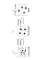
- the mixing step is a step of preparing a mixture (slurry liquid) of a polymerizable monomer, conductive particles, a reaction initiator, and a solvent (FIG. 1 (a)).
- any material other than the polymerizable monomer, conductive particles, reaction initiator, and solvent may be blended according to the purpose.
- a polymerizable monomer and electroconductive particle it can select suitably according to the objective, About those details, it is as having mentioned above in description of the insulation coating particle.
- the reaction initiator is not particularly limited as long as it can dissolve in the solvent and start the polymerization reaction of the polymerizable monomer, and a known reaction initiator can be appropriately used.
- Specific examples of the reaction initiator include thermal polymerization initiators such as azo compounds and organic peroxides; ultraviolet polymerization initiators such as alkylphenone types and acylphosphine oxide types; among these, among these
- an azo compound or an organic peroxide is preferably used.
- a reaction initiator may be used individually by 1 type, and may be used in combination of 2 or more type.
- the solvent is not particularly limited as long as it can dissolve the polymerizable monomer and the reaction initiator described above, and a known solvent can be appropriately used.
- specific examples of the solvent include hexane, cyclohexane, diethyl ether, polyether (glyme), ⁇ -butyrolactone, N-methylpyrrolidone, acetonitrile, tetrahydrofuran, ethyl acetate, xylene, toluene, benzene, dimethyl sulfoxide, acetone, Examples include methyl ethyl ketone, ethanol, methanol, water and the like.
- a solvent may be used individually by 1 type and may be used in combination of 2 or more type.
- the solvent has a solubility of the polymerizable monomer in the mixture described above, and the polymerizable monomer is polymerized. It is preferable that it is higher than the solubility of the polymer formed. From the same viewpoint, the solvent dissolves the polymerizable monomer in the above-described mixture, but it is more preferable that the solvent does not dissolve the polymer obtained by polymerizing the polymerizable monomer. As the solvent is a good solvent for the polymerizable monomer, the polymerization reaction is promoted, and the solvent is a poor solvent for the polymer obtained by polymerizing the polymerizable monomer.
- divinylbenzene when divinylbenzene is used as the polymerizable monomer, it is preferable to use ethanol or a mixture of ethanol and isopropyl alcohol as the solvent.
- a (meth) acrylate compound when using a (meth) acrylate compound as a polymerizable monomer, it is preferable to use ethanol or a mixture of ethanol and toluene as a solvent.
- a deaeration process is an arbitrary process in the manufacturing method of the insulation coating particle
- the inerting step is an optional step in the method for producing insulating coated particles of the present invention, and is a step of inerting the mixture after the mixing step or before or after the optional degassing step (FIG. 1 ( c)).
- the method of inerting is not particularly limited, and examples thereof include a method of supplying an inert gas such as nitrogen by bubbling while stirring the mixture.
- An energy provision process is a process of giving energy to the said mixture, stirring a mixture after a mixing process or arbitrary deaeration processes or an inertization process.
- the polymerization reaction starts, the polymerizable monomer is polymerized, and an insulating polymer is generated.
- the insulating polymer adheres to at least a part of the surface of the conductive particles in the mixture, and insulating coating particles are generated.
- the mixing step the polymerizable monomer, the conductive particles, the reaction initiator, and the solvent are mixed, and in this energy application step, the mixture is mixed.
- the insulating coating particles finally obtained are formed with a coating having a better insulating property than the conventional one. As a result, the insulating property is greatly improved while maintaining high electrical conductivity.
- Examples of the energy applied to the mixture include thermal energy and light energy such as ultraviolet rays, and the type of the above-described reaction initiator can be appropriately selected depending on the type of energy.
- thermal energy to the mixture (that is, to heat the mixture) as shown in FIG.
- thermal energy it is possible to easily and reliably produce the insulating polymer.
- a method for heating the mixture for example, as shown in FIG. 1 (d), a method of immersing a container containing the mixture in a thermostatic chamber in which temperature management is performed may be mentioned.
- the heating temperature of the mixture is preferably 0 ° C. or higher and 200 ° C. or lower.
- the heating temperature of the mixture is 0 ° C. or higher and 200 ° C. or lower, a polymer having high insulating properties can be generated more reliably.
- the heating temperature of the mixture is more preferably 25 ° C. or higher and 150 ° C. or lower.
- the slow cooling step is an optional step in the method for producing insulating coated particles of the present invention, and is a step of slowly cooling the mixture containing conductive particles to which the insulating polymer is fixed to room temperature after the energy application step. (FIG. 1 (e)).
- the method of slow cooling is not particularly limited, and examples thereof include a method of immersing a container containing the mixture in a cooling tank while controlling the temperature, as shown in FIG.
- the mechanism by which the insulating polymer adheres to the surface of the conductive particles by the above-described energy application step and optional slow cooling step will be discussed below with reference to the drawings.
- the energy application step that is, before the polymerization reaction starts
- the conductive particles and the polymerizable monomer are present in the mixture in a state of being dispersed or dissolved in a solvent (FIG. 2A).
- the polymerizable monomer is polymerized in the mixture, polymerized to the precipitation critical chain length in the solvent, and then the conductive particles are used as a trigger (nucleus) for precipitation.
- an insulating polymer is deposited on the surface of the conductive particles (FIG. 2B).
- the generated insulating polymer is insoluble in the solvent or very little if dissolved when taken as a whole.
- the polymerizable monomer reacts with the insulating polymer, and further precipitation occurs, and the physical properties on the surface of the conductive particles are reduced.
- a stack of mechanical and chemical insulating polymers is expected. Thereafter, when the slow cooling step is performed, the solubility of the insulating polymer in the solvent decreases.
- the insulating polymer dissolved in a small amount in the solvent has a thickness of the insulating polymer on the surface of the conductive particles. Contributing to the increase and easing the contribution can reduce the unifying concern (FIG. 2 (c)). And, in the method for producing insulating coated particles according to one embodiment of the present invention, the selectivity to the surface of the conductive particles is high compared to emulsion polymerization embedded by random phase separation, and the insulating polymer is uniform. Coating (adhesion) becomes possible. And the produced
- the manufacturing method of the insulation coating particle which concerns on one Embodiment of this invention includes the reaction which deposits an insulating polymer on the surface of electroconductive particle, This reaction approximates precipitation polymerization.
- this reaction is different from ordinary precipitation polymerization in that it is not a mechanism mainly caused by electrostatic attraction / adsorption, absorption of monomers or initiator components, bonding by surface functional groups, etc. .
- FIG. 2 shows that the entire surface of the conductive particles is covered with an insulating polymer.
- this diagram is merely a schematic diagram, and in practice, the surface of the conductive particles is a part of the surface. The part can be covered with an insulating polymer.
- the coating thickness of the insulating polymer on the surface of the conductive particles is larger when the divinylbenzene is used as the polymerizable monomer than when the (meth) acrylate compound is used as the polymerizable monomer. Can be enlarged.
- a sedimentation process is an arbitrary process in the manufacturing method of the insulation coating particle of this invention, and is a process of sedimenting the obtained insulation coating particle after an energy provision process or an arbitrary slow cooling process (FIG.1 (f)). ). By performing the sedimentation step, the insulating coating particles and the solvent can be easily separated.
- the method of sedimentation is not particularly limited, and examples thereof include a method of allowing a container to stand for a certain time.
- the supernatant removal step is an optional step in the method for producing insulating coated particles of the present invention, and is a step of removing the supernatant after an optional sedimentation step (not shown).
- the method for removing the supernatant is not particularly limited, and examples thereof include decantation.
- the solid-liquid separation step is an optional step in the method for producing insulating coated particles of the present invention, and after the energy application step, or after the optional slow cooling step or the cleaning step described later, the solid content containing the insulating coated particles. Is a step of separating the liquid from the liquid (not shown).
- the method for solid-liquid separation is not particularly limited, and examples thereof include suction filtration.
- the washing step is an optional step in the method for producing insulating coated particles of the present invention, and is a step of washing the solid content after an optional supernatant removing step or solid-liquid separation step (not shown).
- the washing method is not particularly limited, and examples thereof include a method of adding an arbitrary solvent and stirring.
- a drying process is an arbitrary process in the manufacturing method of the insulation coating particle
- the polymer coverage in the obtained insulation-coated particles is, for example, selecting an appropriate solvent that adjusts the control temperature during the reaction. For example, it can be adjusted by controlling the deposition rate of the polymer. Specifically, when the deposition rate of the polymer is increased, the homogeneity is lowered and the coverage is lowered.
- the average coating thickness of the polymer in the obtained insulating coated particles is, for example, the combination of a polymerizable monomer, a reaction initiator, and a solvent in the mixing step.
- Adjust the ratio adjust the amount of energy applied (for example, heating temperature) in the energy application step, select an appropriate solvent, focusing on the solubility of the insulating polymer produced by the polymerization, focus on the polymerization reaction rate Then, it can be adjusted by selecting an appropriate polymerizable monomer.
- the particle-containing composition of the present invention is characterized by containing the above-described insulating coating particles of the present invention. Since the particle-containing composition of the present invention contains the above-described insulating coating particles of the present invention, it has excellent electrical conductivity while providing high electrical conductivity. In addition, it is not specifically limited about components other than the insulation coating particle contained in the particle
- the anisotropic conductive adhesive of the present invention includes the above-described particle-containing composition of the present invention.
- the anisotropic conductive adhesive of the present invention may be the particle-containing composition itself of the present invention described above or may further contain any component other than the above-described particle-containing composition of the present invention, For example, a curable resin such as an epoxy resin, a curing agent, an organic solvent, and the like can be further included.
- the anisotropic conductive adhesive of this invention can be made into a film form (an anisotropic conductive adhesive film may be sufficient).
- An anisotropic conductive adhesive film for example, at least the insulating coating particles of the present invention, a curable resin such as an epoxy resin, a curing agent and an organic solvent are mixed, the resulting mixture is applied in layers, and then the coating film obtained Can be prepared by volatilizing the organic solvent.
- a curable resin such as an epoxy resin, a curing agent and an organic solvent
- the anisotropic conductive adhesive of the present invention includes the above-described particle-containing composition of the present invention, that is, includes at least the above-described insulating coating particles of the present invention. . More specifically, the anisotropic conductive adhesive of the present invention is an insulating coated particle that is not originally coated with an insulating polymer when placed between a circuit board with terminals facing each other and pressed. Through the surface (surface of the conductive particles) and / or the surface where the fixed insulating polymer is excluded by the pressure at the time of pressure bonding, excellent electrical conductivity can be provided between the opposing terminals.
- Examples 1 to 7 Into a glass container, the amount of conductive particles shown in Table 1 (manufactured by Sekisui Chemical Co., Ltd., “AUL704”) and 95% of the amount of ethanol shown in Table 1 as a solvent were added, and then a stirring blade was used. And mixed to prepare a slurry. To this slurry liquid, nitrogen was added at a flow rate of 160 mL / min to carry out inerting, and polymerizable monomers shown in Table 1 were added in an amount shown in Table 1.
- the reaction initiator oil-soluble azo compound
- the reaction initiator oil-soluble azo compound
- a mixture of a polymerizable monomer, conductive particles, a reaction initiator, and a solvent was prepared.
- the inerting with nitrogen was stopped.
- the mixture was heated to 70 ° C. with stirring (ie, heat energy was applied to the mixture) and maintained for 3 hours, and then gradually cooled to 40 ° C.
- FIG. 3 shows an image obtained by scanning electron microscope (SEM) of the insulating coating particles according to Example 1.
- FIG. 3A is a medium magnification image
- FIG. 3B is a high magnification image.
- the obtained insulating coating particles were evaluated for the average coating thickness, the coverage, and the adhesion of the polymer according to the following methods (1) to (3).
- anisotropic conductive adhesive film using toluene
- MEK methyl ethyl ketone
- a crosslinked acrylic resin (manufactured by Soken Chemical Co., Ltd., trade name: MP series) was prepared as a polymer for coating the surface of the conductive particles. 4 g of this cross-linked acrylic resin and 20 g of conductive particles (Sekisui Chemical Co., Ltd., “AUL704”) were introduced into a hybridizer (trade name: NHS series, manufactured by Nara Machinery Co., Ltd.). The conductive particles were coated with a polymer to obtain coated particles. In addition, as processing conditions in the hybridizer, the rotational speed was 16000 / min, the reaction vessel temperature was 60 ° C., and the hybridizer was operated until a desired coating thickness was obtained.
- FIG. 4 shows an image of the coated particles according to Comparative Example 2 by a scanning electron microscope (SEM).
- SEM scanning electron microscope
- 4A is a medium magnification image
- FIG. 4B is a high magnification image.
- various evaluations were performed in the same manner as in Examples 1 to 7, except that the coated particles were used instead of the insulating coated particles.
- an IC substrate having a width of 1.8 mm, a length of 20 mm, and a thickness of 0.5 mm was provided, and a plurality of gold-plated bumps were formed in a straight array along one side edge.
- An IC was prepared. Each bump was 30 ⁇ m ⁇ 85 ⁇ m and had a thickness of 15 ⁇ m.
- an ITO pattern glass having an electrode pattern having a thickness of 0.7 mm and the same size and the same pitch as the bumps of the IC was prepared as a glass substrate for conductivity evaluation. And after attaching an anisotropic conductive adhesive film temporarily to this glass substrate, the connection body sample was produced from the bump in IC, and the electrode in a glass substrate.
- thermocompression bonding conditions were 170 ° C., 60 MPa, 5 sec / Teflon (registered trademark) 50 ⁇ m.
- electrical_connection resistance when the electric current of 1 mA was sent for 500 h on 85 degreeC and 85% RH conditions was measured.
- Table 1 The results are shown in Table 1.
- an IC substrate having a width of 1.5 mm, a length of 130 mm, and a thickness of 0.5 mm was provided, and a plurality of gold-plated bumps were formed in a single-row straight array along one side edge.
- An IC was prepared. In this IC, the thickness of each bump was 15 ⁇ m, and the space between the bumps was 10 ⁇ m.
- an ITO pattern glass was prepared in which a comb-like electrode pattern having a thickness of 0.5 mm and the same size and pitch as the IC bumps was formed.
- thermocompression bonding conditions were 170 ° C., 60 MPa, 5 sec / Teflon (registered trademark) 50 ⁇ m.
- the resistance value between adjacent bumps was measured by the 2 terminal method.
- 8 electrode patterns composed of 10 sets of bumps were formed on the IC, and the number of electrode patterns in which one or more sets of 10 shorts occurred was counted.
- Examples 1 to 7 using the insulating coating particles in which the insulating polymer is fixed to at least a part of the surface of the conductive particles are excellent in both conductivity and insulation.
- the insulating coating particle according to the example has the insulating polymer firmly attached to at least a part of the surface of the conductive particle.
- Comparative Example 1 using particles not coated with an insulating polymer is at least inferior in insulating properties.
- the polymer cannot be firmly attached to the surface of the conductive particles, and the coated polymer is made of an anisotropic conductive adhesive film. This may be due to erosion by the solvent used in the preparation.
- the present invention when circuit boards having a plurality of terminals are electrically connected to each other, electrical conductivity is ensured between opposing terminals while sufficiently ensuring insulation between adjacent terminals on each board.
- Insulating coated particles capable of obtaining the resulting anisotropic conductive adhesive, and a particle-containing composition and an anisotropic conductive adhesive including the insulating coated particles can be provided.
- the manufacturing method of the insulation coating particle which can manufacture the insulation coating particle mentioned above efficiently can be provided.
Landscapes
- Chemical & Material Sciences (AREA)
- Engineering & Computer Science (AREA)
- Spectroscopy & Molecular Physics (AREA)
- Manufacturing & Machinery (AREA)
- Physics & Mathematics (AREA)
- Dispersion Chemistry (AREA)
- Organic Chemistry (AREA)
- Life Sciences & Earth Sciences (AREA)
- Materials Engineering (AREA)
- Wood Science & Technology (AREA)
- Non-Insulated Conductors (AREA)
- Adhesives Or Adhesive Processes (AREA)
- Conductive Materials (AREA)
Abstract
複数の端子を備える回路基板同士を電気的に接続させた場合に、各基板上で隣接する端子間の絶縁性を十分に確保しつつ、対向する端子間に導通性をもたらす異方性導電接着剤を得ることが可能な、絶縁被覆粒子を提供する。絶縁被覆粒子は、導電性粒子の表面の少なくとも一部に、重合性単量体に由来する構造単位を含む絶縁性重合体が固着されていることを特徴とする。
Description
本出願は、日本国特許出願2016-135394号(2016年7月7日出願)の優先権を主張するものであり、当該出願の開示全体を、ここに参照のために取り込む。
本発明は、絶縁被覆粒子、絶縁被覆粒子の製造方法、粒子含有組成物、及び異方性導電接着剤に関するものである。
従来より、複数の端子を備える回路基板同士を、それぞれの端子を介して電気的に接続するのに、硬化性樹脂などのバインダ中に導電性粒子を分散させてなる異方性導電接着剤を用いた接続方式が採用されている。この異方性導電接着剤は、それぞれの端子を対向させた回路基板の間に配置して、ヒーターなどで熱圧着することで、対向する端子間に導電性粒子を介して導通性をもたらしつつ、各基板上で隣接する端子間の絶縁性を保持する機能を有する。
ここで、昨今、モバイル機器などの装置の小型化及び高性能化が要求されている。かかる要求に応じるため、当該装置に用いられる近年の回路基板は、各端子の接続面が小面積化されているとともに、回路基板の単位面積当たりの端子数が増加している。すなわち、上述の回路基板は、隣接する端子間の距離が短い傾向にある。
このような、隣接する端子間の距離が短い回路部材同士を、異方性導電接着剤で接合し、十分な量の導電性粒子を介在させて導通性を確保するためには、バインダ中の導電性粒子の密度を高める必要がある。しかしながら、バインダ中の導電性粒子の密度を高めると、隣接する端子間で、ショートが発生し易くなる。
かかる事態への対処として、例えば特許文献1には、導電性粒子表面に絶縁性樹脂を被覆しておくことで、隣接する端子間でのショートを防ぐとともに、対向する端子間では、圧着時の圧力により導電性粒子表面の絶縁性樹脂が排除されて、導通性を確保することができることが開示されている。そして、このような絶縁性樹脂が被覆された導電性粒子は、特許文献1,2に開示されるように、ハイブリタイザー等を用いた乾式法により、製造することができることが知られている。
しかしながら、上述したような絶縁性樹脂が被覆された導電性粒子を使用して、フィルム状又はペースト状の異方性導電接着剤を製造すると、場合により、導電性粒子を被覆している絶縁性樹脂の層が製造時に使用する溶剤で膨潤、溶解、又は変形を引き起こすという問題があった。このような場合には、異方性導電接着剤の導通性及び絶縁性の少なくともいずれかに悪影響が生じていた。
更に、上記従来の乾式法では、粒子表面に十分な固着性を有する皮膜を形成することが困難であり、そのため、粒子表面に対する皮膜の被覆率が頭打ちとなり、絶縁性そのものを十分に高めることができなかった。
加えて、上記従来の乾式法は、歩留まりが十分でなく、バッチ当たりの処理量を増大させることに限界がある、という問題も抱えていた。
本発明は、かかる事情に鑑みてなされたものであって、複数の端子を備える回路基板同士を電気的に接続させた場合に、各基板上で隣接する端子間の絶縁性を十分に確保しつつ、対向する端子間に導通性をもたらす異方性導電接着剤を得ることが可能な、絶縁被覆粒子、並びに、当該絶縁被覆粒子を含む、粒子含有組成物及び異方性導電接着剤を提供することを目的とする。また、本発明は、上述した絶縁被覆粒子を効率的に製造することが可能な、絶縁被覆粒子の製造方法を提供することを目的とする。
本発明者らは、上記の課題を解決するべく、鋭意研究を重ねた。その結果、導電性粒子の表面に絶縁性物質が強固に付着された粒子が、異方性導電接着剤に優れた絶縁性と異方的導電性とをもたらすことができること、並びに、このような粒子は、乾式法に代わる新たな方法を用いることにより得られることを見出し、本発明の完成に至った。
本発明は、本発明者らによる前記知見に基づくものであり、前記課題を解決するための
手段としては以下の通りである。
[1]導電性粒子の表面の少なくとも一部に、重合性単量体に由来する構造単位を含む絶縁性重合体が固着されていることを特徴とする、絶縁被覆粒子。
上記構成によって、絶縁性を十分に確保しつつ、導通性をもたらす異方性導電接着剤を得ることができる。
[2]前記絶縁性重合体の被覆率が40%超である、前記[1]に記載の絶縁被覆粒子。
[3]前記重合性単量体が、2つ以上の重合性官能基を有する単量体を含む、前記[1]又は[2]に記載の絶縁被覆粒子。
[4]前記2つ以上の重合性官能基を有する単量体が、ジビニルベンゼンである、前記[3]に記載の絶縁被覆粒子。
[5]前記2つ以上の重合性官能基を有する単量体が、(メタ)アクリレート化合物である、前記[3]に記載の絶縁被覆粒子。
[6]前記絶縁性重合体の平均被覆厚みが、50nm以上である、前記[1]~[5]のいずれかに記載の絶縁被覆粒子。
[7]重合性単量体、導電性粒子、及び反応開始剤と、溶媒との混合物を調製する工程と、
前記混合物を撹拌しながら該混合物にエネルギーを付与することにより、前記重合性単量体が重合されてなる絶縁性重合体を生成するとともに、前記導電性粒子の表面の少なくとも一部に、前記絶縁性重合体を固着させる工程と、
を含むことを特徴とする、絶縁被覆粒子の製造方法。
上記構成によって、上述した絶縁被覆粒子を効率的に製造することができる。
[8]前記溶媒は、前記重合性単量体を溶解するが、前記絶縁性重合体を溶解しない溶媒である、前記[7]に記載の絶縁被覆粒子の製造方法。
[9]前記エネルギーが熱エネルギーである、前記[7]又は[8]に記載の絶縁被覆粒子の製造方法。
[10]前記[1]~[6]のいずれかに記載の絶縁被覆粒子を含むことを特徴とする、粒子含有組成物。
[11]前記[10]に記載の粒子含有組成物を含むことを特徴とする、異方性導電接着剤。
手段としては以下の通りである。
[1]導電性粒子の表面の少なくとも一部に、重合性単量体に由来する構造単位を含む絶縁性重合体が固着されていることを特徴とする、絶縁被覆粒子。
上記構成によって、絶縁性を十分に確保しつつ、導通性をもたらす異方性導電接着剤を得ることができる。
[2]前記絶縁性重合体の被覆率が40%超である、前記[1]に記載の絶縁被覆粒子。
[3]前記重合性単量体が、2つ以上の重合性官能基を有する単量体を含む、前記[1]又は[2]に記載の絶縁被覆粒子。
[4]前記2つ以上の重合性官能基を有する単量体が、ジビニルベンゼンである、前記[3]に記載の絶縁被覆粒子。
[5]前記2つ以上の重合性官能基を有する単量体が、(メタ)アクリレート化合物である、前記[3]に記載の絶縁被覆粒子。
[6]前記絶縁性重合体の平均被覆厚みが、50nm以上である、前記[1]~[5]のいずれかに記載の絶縁被覆粒子。
[7]重合性単量体、導電性粒子、及び反応開始剤と、溶媒との混合物を調製する工程と、
前記混合物を撹拌しながら該混合物にエネルギーを付与することにより、前記重合性単量体が重合されてなる絶縁性重合体を生成するとともに、前記導電性粒子の表面の少なくとも一部に、前記絶縁性重合体を固着させる工程と、
を含むことを特徴とする、絶縁被覆粒子の製造方法。
上記構成によって、上述した絶縁被覆粒子を効率的に製造することができる。
[8]前記溶媒は、前記重合性単量体を溶解するが、前記絶縁性重合体を溶解しない溶媒である、前記[7]に記載の絶縁被覆粒子の製造方法。
[9]前記エネルギーが熱エネルギーである、前記[7]又は[8]に記載の絶縁被覆粒子の製造方法。
[10]前記[1]~[6]のいずれかに記載の絶縁被覆粒子を含むことを特徴とする、粒子含有組成物。
[11]前記[10]に記載の粒子含有組成物を含むことを特徴とする、異方性導電接着剤。
本発明によれば、複数の端子を備える回路基板同士を電気的に接続させた場合に、各基板上で隣接する端子間の絶縁性を十分に確保しつつ、対向する端子間に導通性をもたらす異方性導電接着剤を得ることが可能な、絶縁被覆粒子、並びに、当該絶縁被覆粒子を含む、粒子含有組成物及び異方性導電接着剤を提供することできる。また、本発明によれば、上述した絶縁被覆粒子を効率的に製造することが可能な、絶縁被覆粒子の製造方法を提供することができる。
以下、本発明について、実施形態に基づき具体的に説明する。
<絶縁被覆粒子>
本発明の一実施形態に係る絶縁被覆粒子は、少なくとも、導電性粒子と、重合性単量体に由来する構造単位を含む絶縁性重合体とを備え、導電性粒子の表面の少なくとも一部に、上述の絶縁性重合体が固着されていることを特徴とする。
導電性粒子の表面に固着可能な絶縁性重合体は、溶剤に対する溶解性が低く、また、導電性粒子の表面に固着された(即ち、強固に付着した)重合体は、溶剤に接触するなどしたとしても、剥落し難い。そのため、本発明の一実施形態に係る絶縁被覆粒子は、異方性導電接着剤の作製時において、導電性粒子の表面からの重合体の剥落、及び、使用する溶剤による導電性粒子表面の重合体への侵食が抑制されており、異方性導電接着剤における絶縁性(以下、これを単に「絶縁性」と称することがある。)を高く保持することができる。
また、本発明の一実施形態に係る絶縁被覆粒子は、異方性導電接着剤に分散させ、端子を対向させた回路基板の間にこの異方性導電接着剤を配置し、圧着させたときに、重合体がもともと被覆されていない表面(導電性粒子の表面)、及び/又は、固着されていた重合体が圧着時の圧力により排除された表面を介して、対向する端子間に優れた導通性(以下、これを単に「導通性」と称することがある。)をもたらすことができる。
そして、本発明の一実施形態に係る絶縁被覆粒子は、例えば、後述する本発明の一実施形態に係る絶縁被覆粒子の製造方法により、製造することができる。
本発明の一実施形態に係る絶縁被覆粒子は、少なくとも、導電性粒子と、重合性単量体に由来する構造単位を含む絶縁性重合体とを備え、導電性粒子の表面の少なくとも一部に、上述の絶縁性重合体が固着されていることを特徴とする。
導電性粒子の表面に固着可能な絶縁性重合体は、溶剤に対する溶解性が低く、また、導電性粒子の表面に固着された(即ち、強固に付着した)重合体は、溶剤に接触するなどしたとしても、剥落し難い。そのため、本発明の一実施形態に係る絶縁被覆粒子は、異方性導電接着剤の作製時において、導電性粒子の表面からの重合体の剥落、及び、使用する溶剤による導電性粒子表面の重合体への侵食が抑制されており、異方性導電接着剤における絶縁性(以下、これを単に「絶縁性」と称することがある。)を高く保持することができる。
また、本発明の一実施形態に係る絶縁被覆粒子は、異方性導電接着剤に分散させ、端子を対向させた回路基板の間にこの異方性導電接着剤を配置し、圧着させたときに、重合体がもともと被覆されていない表面(導電性粒子の表面)、及び/又は、固着されていた重合体が圧着時の圧力により排除された表面を介して、対向する端子間に優れた導通性(以下、これを単に「導通性」と称することがある。)をもたらすことができる。
そして、本発明の一実施形態に係る絶縁被覆粒子は、例えば、後述する本発明の一実施形態に係る絶縁被覆粒子の製造方法により、製造することができる。
なお、本明細書において、重合体が粒子の表面に「固着されている」とは、重合体により表面が被覆された粒子10gを50mlの蒸留水に分散させ、振とうし、静置させた後、この液の上澄み液を目視にて確認したときに、濁っていることが確認されない程度に、重合体が粒子の表面に強固に付着していることを指す。そして、粒子の表面に関する「固着」の語は、本明細書において、「被覆」の下位概念としても用いられる語である。
(導電性粒子)
本発明の一実施形態に係る絶縁被覆粒子が備える導電性粒子としては、特に限定されず、例えば、異方性導電接着剤に使用される公知の任意の導電性粒子を用いることができる。具体的には、導電性粒子としては、ニッケル、鉄、銅、アルミニウム、錫、鉛、クロム、コバルト、銀、金等の各種金属又は金属合金の粒子;金属酸化物、カーボン、グラファイト、ガラス、セラミック、プラスチック、樹脂等の粒子の表面に金属をコートしたもの;等が挙げられる。ここで、樹脂粒子の表面に金属をコートしたものである場合、樹脂粒子としては、例えば、エポキシ樹脂、フェノール樹脂、アクリル樹脂、アクリロニトリル・スチレン(AS)樹脂、ベンゾグアナミン樹脂、ジビニルベンゼン系樹脂、スチレン系樹脂等の粒子が挙げられる。導電性粒子は、一種単独であってもよく、二種以上を組み合わせたものであってもよい。
また、導電性粒子の形状、大きさとしては、特に限定されず、目的に応じて適宜選択することができる。
本発明の一実施形態に係る絶縁被覆粒子が備える導電性粒子としては、特に限定されず、例えば、異方性導電接着剤に使用される公知の任意の導電性粒子を用いることができる。具体的には、導電性粒子としては、ニッケル、鉄、銅、アルミニウム、錫、鉛、クロム、コバルト、銀、金等の各種金属又は金属合金の粒子;金属酸化物、カーボン、グラファイト、ガラス、セラミック、プラスチック、樹脂等の粒子の表面に金属をコートしたもの;等が挙げられる。ここで、樹脂粒子の表面に金属をコートしたものである場合、樹脂粒子としては、例えば、エポキシ樹脂、フェノール樹脂、アクリル樹脂、アクリロニトリル・スチレン(AS)樹脂、ベンゾグアナミン樹脂、ジビニルベンゼン系樹脂、スチレン系樹脂等の粒子が挙げられる。導電性粒子は、一種単独であってもよく、二種以上を組み合わせたものであってもよい。
また、導電性粒子の形状、大きさとしては、特に限定されず、目的に応じて適宜選択することができる。
(絶縁性重合体)
本発明の一実施形態に係る絶縁被覆粒子が備える絶縁性重合体(以下、単に「重合体」と称することがある。)は、重合性単量体に由来する構造単位を含み、導電性粒子の表面の少なくとも一部に固着されている。
なお、本明細書において、「重合性単量体」とは、熱エネルギーや紫外線エネルギー等のエネルギーが付与されることにより重合する性質を持つ化合物を指し、通常は二重結合を有する化合物である。また、重合性単量体は、一種単独であってもよく、二種以上を組み合わせたものであってもよい。
本発明の一実施形態に係る絶縁被覆粒子が備える絶縁性重合体(以下、単に「重合体」と称することがある。)は、重合性単量体に由来する構造単位を含み、導電性粒子の表面の少なくとも一部に固着されている。
なお、本明細書において、「重合性単量体」とは、熱エネルギーや紫外線エネルギー等のエネルギーが付与されることにより重合する性質を持つ化合物を指し、通常は二重結合を有する化合物である。また、重合性単量体は、一種単独であってもよく、二種以上を組み合わせたものであってもよい。
本発明の一実施形態に係る絶縁被覆粒子において、重合性単量体は、2つ以上の重合性官能基を有する単量体を含むことが好ましい。これにより、得られる重合体は、いわゆる三次元網目構造が形成されており、溶剤(メチルエチルケトン及び酢酸エチル等の低沸点の溶剤、並びにトルエン等の高沸点の溶剤を含む)に対する溶解性が一層低くなるため、十分に高い絶縁性を保持することができる。
なお、本明細書において「重合性官能基」とは、硬化の際に重合反応及び/又は架橋反応に用いられる基を指す。また、重合性単量体が有する重合性官能基は、一種単独であってもよく、二種以上を組み合わせたものであってもよい。
なお、本明細書において「重合性官能基」とは、硬化の際に重合反応及び/又は架橋反応に用いられる基を指す。また、重合性単量体が有する重合性官能基は、一種単独であってもよく、二種以上を組み合わせたものであってもよい。
重合性官能基として、具体的には、ビニル基、アリル基、(メタ)アクリロイル基、等が挙げられる。また、2つ以上の重合性官能基を有する単量体として、具体的には、ジビニル化合物等のビニル化合物、ジアリル化合物等のアリル化合物、ジ(メタ)アクリレート化合物等の(メタ)アクリレート化合物、などが挙げられる。そして、本発明の一実施形態に係る絶縁被覆粒子においては、より優れた絶縁性を得る観点から、2つ以上の重合性官能基を有する単量体が、ビニル化合物、特にはジビニルベンゼンであることが好ましく、また、(メタ)アクリレート化合物であることも好ましい。
なお、本明細書において、「(メタ)アクリロイル基」とは、アクリロイル基及びメタアクリロイル基のうちの少なくともいずれかを指し、「(メタ)アクリレート」とは、アクリレート及びメタアクリレートのうちの少なくともいずれかを指す。
なお、本明細書において、「(メタ)アクリロイル基」とは、アクリロイル基及びメタアクリロイル基のうちの少なくともいずれかを指し、「(メタ)アクリレート」とは、アクリレート及びメタアクリレートのうちの少なくともいずれかを指す。
2つ以上の重合性官能基を有する単量体である(メタ)アクリレート化合物としては、例えば、エチレングリコールジ(メタ)アクリレート、(ポリ)エチレングリコールジ(メタ)アクリレート、プロピレングリコールジ(メタ)アクリレート、(ポリ)プロピレングリコールジ(メタ)アクリレート、ペンタエリスリトールテトラ(メタ)アクリレート、ペンタエリスリトールトリ(メタ)アクリレート、ペンタエリスリトールジ(メタ)アクリレート、トリメチロールプロパントリ(メタ)アクリレート、ジペンタエリスリトールヘキサ(メタ)アクリレート、ジペンタエリスリトールペンタ(メタ)アクリレート、グリセロールトリ(メタ)アクリレート、グリセロールジ(メタ)アクリレート、1,6-ヘキサンジオールジ(メタ)アクリレート、ネオペンチルグリコールジ(メタ)アクリレート、テトラメチロールメタントリ(メタ)アクリレート、テトラメチロールプロパンテトラ(メタ)アクリレート、トリシクロデカンジメタノールジ(メタ)アクリレート、(ポリ)エトキシ化ビスフェノールAジ(メタ)アクリレート等が挙げられる。
なお、重合体は、上述した重合性単量体に由来する構造単位以外の構造単位を含んでいてもよい。ただし、重合体は、優れた絶縁性を確保する観点から、重合性単量体に由来する構造単位の割合が50質量%以上であることが好ましく、90質量%以上であることがより好ましい。
重合体は、異方性導電接着剤の調製時における乾燥温度で、異方性導電接着剤の調製に使用する溶剤にほとんど溶解しないことが好ましい。例えば、重合体は、50℃でのメチルエチルケトン100gに対する溶解量が0.1g以下であることが好ましく、50℃での酢酸エチル100gに対する溶解量が0.1g以下であることが好ましく、また、70℃でのトルエン100gに対する溶解量が0.1g以下であることが好ましい。これらの少なくともいずれかの特徴を満たすことにより、異方性導電接着剤の調製時に使用する溶剤による重合体の侵食を、より確実に回避することができる。なお、これらの特徴は、例えば、上述した2つ以上の重合性官能基を有する単量体を用いて重合させることにより、達成することができる。
(絶縁被覆粒子の構造)
本発明の一実施形態に係る絶縁被覆粒子は、重合体の被覆率が、40%超であることが好ましい。重合体の被覆率が40%超であることにより、十分に高い絶縁性を確保することができる。
また、本発明の一実施形態に係る絶縁被覆粒子は、特に限定されず、重合体の被覆率が75%以下であることが、導通性の悪化を効果的に抑制する観点から好ましい。
なお、本明細書において、重合体の「被覆率」とは、導電性粒子の全表面積のうち、重合体で被覆された部分の面積の割合を指し、本明細書の実施例に記載された方法により、求めることができる。
本発明の一実施形態に係る絶縁被覆粒子は、重合体の被覆率が、40%超であることが好ましい。重合体の被覆率が40%超であることにより、十分に高い絶縁性を確保することができる。
また、本発明の一実施形態に係る絶縁被覆粒子は、特に限定されず、重合体の被覆率が75%以下であることが、導通性の悪化を効果的に抑制する観点から好ましい。
なお、本明細書において、重合体の「被覆率」とは、導電性粒子の全表面積のうち、重合体で被覆された部分の面積の割合を指し、本明細書の実施例に記載された方法により、求めることができる。
本発明の一実施形態に係る絶縁被覆粒子は、重合体の平均被覆厚みが、50nm以上であることが好ましい。固着されている重合体の平均被覆厚みが50nm以上であることにより、絶縁性を十分に高めることができる。
また、本発明の一実施形態に係る絶縁被覆粒子は、導通性を確保する観点から、重合体の平均被覆厚みが、500nm以下であることが好ましく、350nm以下であることがより好ましく、250nm以下であることが更に好ましい。
なお、本明細書において、重合体の「平均被覆厚み」とは、表面を被覆する重合体の厚みの平均値を指し、本明細書の実施例に記載された方法により、測定することができる。
また、本発明の一実施形態に係る絶縁被覆粒子は、導通性を確保する観点から、重合体の平均被覆厚みが、500nm以下であることが好ましく、350nm以下であることがより好ましく、250nm以下であることが更に好ましい。
なお、本明細書において、重合体の「平均被覆厚み」とは、表面を被覆する重合体の厚みの平均値を指し、本明細書の実施例に記載された方法により、測定することができる。
<絶縁被覆粒子の製造方法>
本発明の絶縁被覆粒子の製造方法は、少なくとも、混合工程と、エネルギー付与工程とを含み、更に必要に応じて、脱気工程、イナート化工程、徐冷工程、沈降工程、上澄み除去工程、洗浄工程、固液分離工程、乾燥工程を含む。ここで、本発明の絶縁被覆粒子の製造方法は、いわゆる湿式法に分類され、また、従来の乾式法に比べ、歩留まりを十分に高めるとともに、バッチ当たりの処理量を十分に高めることが可能な、効率的な方法である。
以下、本発明の一実施形態に係る絶縁被覆粒子の製造方法について説明する。
本発明の絶縁被覆粒子の製造方法は、少なくとも、混合工程と、エネルギー付与工程とを含み、更に必要に応じて、脱気工程、イナート化工程、徐冷工程、沈降工程、上澄み除去工程、洗浄工程、固液分離工程、乾燥工程を含む。ここで、本発明の絶縁被覆粒子の製造方法は、いわゆる湿式法に分類され、また、従来の乾式法に比べ、歩留まりを十分に高めるとともに、バッチ当たりの処理量を十分に高めることが可能な、効率的な方法である。
以下、本発明の一実施形態に係る絶縁被覆粒子の製造方法について説明する。
(混合工程)
混合工程は、重合性単量体、導電性粒子、及び反応開始剤と、溶媒との混合物(スラリー液)を調製する工程である(図1(a))。
また、混合工程では、目的に応じ、重合性単量体、導電性粒子、反応開始剤及び溶媒以外の任意の材料を配合してもよい。
なお、重合性単量体及び導電性粒子については、目的に応じて適宜選択することができ、それらの詳細については、絶縁被覆粒子の説明において上述した通りである。特に、重合性単量体としては、重合により得られる重合体が絶縁性を有するものとなるようなものを選択することが好ましい。
混合工程は、重合性単量体、導電性粒子、及び反応開始剤と、溶媒との混合物(スラリー液)を調製する工程である(図1(a))。
また、混合工程では、目的に応じ、重合性単量体、導電性粒子、反応開始剤及び溶媒以外の任意の材料を配合してもよい。
なお、重合性単量体及び導電性粒子については、目的に応じて適宜選択することができ、それらの詳細については、絶縁被覆粒子の説明において上述した通りである。特に、重合性単量体としては、重合により得られる重合体が絶縁性を有するものとなるようなものを選択することが好ましい。
反応開始剤としては、前記溶媒に溶解し、前記重合性単量体の重合反応を開始することができるものであれば、特に限定されず、公知の反応開始剤を適宜用いることができる。反応開始剤として、具体的には、例えば、アゾ化合物、有機過酸化物等の熱重合開始剤;アルキルフェノン型、アシルフォスフィンオキサイド型等の紫外線重合開始剤;等が挙げられる、これらの中でも、反応開始剤としては、アゾ化合物又は有機過酸化物を用いることが好ましい。
なお、反応開始剤は、一種単独で用いてもよく、二種以上を組み合わせて用いてもよい。
なお、反応開始剤は、一種単独で用いてもよく、二種以上を組み合わせて用いてもよい。
溶媒としては、上述した重合性単量体及び反応開始剤を溶解することができるものであれば、特に限定されず、公知の溶媒を適宜用いることができる。ここで、溶媒の具体例としては、ヘキサン、シクロヘキサン、ジエチルエーテル、ポリエーテル(グライム)、γ―ブチロラクトン、N-メチルピロリドン、アセトニトリル、テトラヒドロフラン、酢酸エチル、キシレン、トルエン、ベンゼン、ジメチルスルホキシド、アセトン、メチルエチルケトン、エタノール、メタノール、水等が挙げられる。溶媒は、一種単独で用いてもよく、二種以上を組み合わせて用いてもよい。
ただし、重合反応を促進するとともに、重合によって得られた絶縁性重合体の性能を高める観点から、溶媒は、上述した混合物中の重合性単量体の溶解度が、当該重合性単量体が重合されてなる重合体の溶解度よりも高いものであることが好ましい。そして、溶媒は、同様の観点から、上述した混合物中の重合性単量体を溶解するが、当該重合性単量体が重合されてなる重合体を溶解しないものであることがより好ましい。溶媒が、重合性単量体に対して良溶媒であることで、重合反応が促進されるとともに、当該重合性単量体が重合されてなる重合体に対して貧溶媒であることで、得られる重合体の再溶解を抑制して、良好に導電性粒子に固着させることができるからである。
なお、上述した、溶解度、或いは、溶解するか否かは、後述するエネルギー付与工程時における混合物の温度で測定或いは判断されるものである。
なお、上述した、溶解度、或いは、溶解するか否かは、後述するエネルギー付与工程時における混合物の温度で測定或いは判断されるものである。
具体的に言うと、重合性単量体としてジビニルベンゼンを用いる場合には、溶媒としては、エタノール又はエタノールとイソプロピルアルコールとの混合物を用いることが好ましい。また、重合性単量体として(メタ)アクリレート化合物を用いる場合には、溶媒としては、エタノール又はエタノールとトルエンとの混合物を用いることが好ましい。
(脱気工程)
脱気工程は、本発明の絶縁被覆粒子の製造方法において任意の工程であり、混合工程で調製した混合物を脱気する工程である(図1(b))。脱気工程を実施することにより、導電性粒子の表面濡れ性を促進することができる。脱気の方法としては、例えば、減圧及び/又は超音波を用いる方法等が挙げられる。
脱気工程は、本発明の絶縁被覆粒子の製造方法において任意の工程であり、混合工程で調製した混合物を脱気する工程である(図1(b))。脱気工程を実施することにより、導電性粒子の表面濡れ性を促進することができる。脱気の方法としては、例えば、減圧及び/又は超音波を用いる方法等が挙げられる。
(イナート化工程)
イナート化工程は、本発明の絶縁被覆粒子の製造方法において任意の工程であり、混合工程の後、或いは、任意の脱気工程の前又は後に、混合物をイナート化する工程である(図1(c))。イナート化工程を実施することにより、後述するエネルギー付与工程における重合反応の阻害を抑制することができる。イナート化の方法としては、特に限定されず、例えば、混合物を撹拌しながら、窒素等の不活性ガスをバブリングにより供給する方法等が挙げられる。
イナート化工程は、本発明の絶縁被覆粒子の製造方法において任意の工程であり、混合工程の後、或いは、任意の脱気工程の前又は後に、混合物をイナート化する工程である(図1(c))。イナート化工程を実施することにより、後述するエネルギー付与工程における重合反応の阻害を抑制することができる。イナート化の方法としては、特に限定されず、例えば、混合物を撹拌しながら、窒素等の不活性ガスをバブリングにより供給する方法等が挙げられる。
(エネルギー付与工程)
エネルギー付与工程は、混合工程、或いは、任意の脱気工程又はイナート化工程の後に、混合物を撹拌しながら、当該混合物にエネルギーを付与する工程である。混合物にエネルギーを付与することにより、重合反応が開始し、重合性単量体が重合されて、絶縁性重合体が生成される。また、これと同時に、絶縁性重合体が、混合物中の導電性粒子の表面の少なくとも一部に固着して、絶縁被覆粒子が生成される。
本発明の一実施形態に係る絶縁被覆粒子の製造方法では、混合工程において、重合性単量体、導電性粒子、及び反応開始剤と、溶媒とを混合するとともに、このエネルギー付与工程において、混合物にエネルギーを付与することによって、導電性粒子同士の凝集を抑制して、所望の厚みを有する絶縁性重合体を導電性粒子上に形成することができる。そして、最終的に得られる絶縁被覆粒子は、従来よりも絶縁性に優れた被覆が形成されている結果、高い導通性は保持しつつ、絶縁性が大きく向上する。
エネルギー付与工程は、混合工程、或いは、任意の脱気工程又はイナート化工程の後に、混合物を撹拌しながら、当該混合物にエネルギーを付与する工程である。混合物にエネルギーを付与することにより、重合反応が開始し、重合性単量体が重合されて、絶縁性重合体が生成される。また、これと同時に、絶縁性重合体が、混合物中の導電性粒子の表面の少なくとも一部に固着して、絶縁被覆粒子が生成される。
本発明の一実施形態に係る絶縁被覆粒子の製造方法では、混合工程において、重合性単量体、導電性粒子、及び反応開始剤と、溶媒とを混合するとともに、このエネルギー付与工程において、混合物にエネルギーを付与することによって、導電性粒子同士の凝集を抑制して、所望の厚みを有する絶縁性重合体を導電性粒子上に形成することができる。そして、最終的に得られる絶縁被覆粒子は、従来よりも絶縁性に優れた被覆が形成されている結果、高い導通性は保持しつつ、絶縁性が大きく向上する。
混合物に付与するエネルギーとしては、例えば、熱エネルギー及び紫外線等の光エネルギー等が挙げられ、エネルギーの種類により、上述した反応開始剤の種類を適切に選択することができる。ただし、本発明の一実施形態に係る絶縁被覆粒子の製造方法では、図1(d)に示すように、混合物に熱エネルギーを付与する(即ち、混合物を加熱する)ことが好ましい。熱エネルギーを用いることにより、絶縁性重合体の生成を容易に且つ確実に行うことができる。混合物を加熱する方法としては、例えば、図1(d)に示すように、混合物を含む容器を温度管理がなされた恒温槽に浸す方法等が挙げられる。
ここで、混合物に熱エネルギーを付与する(即ち、混合物を加熱する)場合において、混合物の加熱温度は、0℃以上200℃以下であることが好ましい。混合物の加熱温度が0℃以上200℃以下であることにより、高い絶縁性を有する重合体の生成をより確実に行うことができる。同様の観点から、混合物の加熱温度は、25℃以上150℃以下であることがより好ましい。
(徐冷工程)
徐冷工程は、本発明の絶縁被覆粒子の製造方法において任意の工程であり、エネルギー付与工程の後に、絶縁性重合体が固着した導電性粒子を含む混合物を、室温まで徐冷する工程である(図1(e))。徐冷工程を実施することにより、溶媒中に微量に溶解した絶縁性重合体を析出させて、絶縁被覆粒子に固着した絶縁性重合体の厚みを増加させることができる。徐冷の方法としては、特に限定されず、例えば、図1(e)に示すように、温度管理をしながら混合物を含む容器を冷却槽に浸す方法等が挙げられる。
徐冷工程は、本発明の絶縁被覆粒子の製造方法において任意の工程であり、エネルギー付与工程の後に、絶縁性重合体が固着した導電性粒子を含む混合物を、室温まで徐冷する工程である(図1(e))。徐冷工程を実施することにより、溶媒中に微量に溶解した絶縁性重合体を析出させて、絶縁被覆粒子に固着した絶縁性重合体の厚みを増加させることができる。徐冷の方法としては、特に限定されず、例えば、図1(e)に示すように、温度管理をしながら混合物を含む容器を冷却槽に浸す方法等が挙げられる。
ここで、上述のエネルギー付与工程及び任意の徐冷工程によって、導電性粒子の表面に絶縁性重合体が固着するメカニズムを、図を用いて以下に考察する。
まず、エネルギー付与工程の前、即ち重合反応が開始する前において、導電性粒子及び重合性単量体は、溶媒に分散又は溶解した状態で混合物中に存在する(図2(a))。そして、エネルギー付与工程で混合物にエネルギーを付与すると、重合性単量体は、混合物中で重合し、溶媒中での析出臨界鎖長まで重合した後に、導電性粒子を析出のきっかけ(核)として、当該導電性粒子の表面に絶縁性重合体が析出する(図2(b))。ここで、生成した絶縁性重合体は、全体として捉えた場合、溶媒に不溶であるか、或いは、溶解したとしてもごく僅かである。そして、析出した絶縁性重合体に重合性官能基が残っている場合には、当該絶縁性重合体に重合性単量体が反応し、またさらに析出が起こり、導電性粒子の表面への物理的及び化学的な絶縁性重合体の積層が期待される。その後、徐冷工程を実施すると、溶媒に対する絶縁性重合体の溶解度が低下する結果、溶媒中に微量に溶解していた絶縁性重合体が、導電性粒子の表面における絶縁性重合体の厚みの増加に寄与し、寄与を緩やかとすることで合一の懸念を低下できる(図2(c))。そして、本発明の一実施形態に係る絶縁被覆粒子の製造方法では、ランダムな相分離によって包埋させるエマルジョン重合などに比べ、導電性粒子の表面への選択性が高く、絶縁性重合体の均一な被覆(固着)が可能となる。そして、生成した絶縁被覆粒子は、従来のものに比べて高い絶縁性を有する。
なお、本発明の一実施形態に係る絶縁被覆粒子の製造方法は、導電性粒子の表面に絶縁性重合体を析出させる反応を含むものであり、この反応は析出重合に近似する。ただし、この反応は、静電的な引力・吸着、単量体や反応開始剤成分の吸収、表面官能基による結合などに主因した機構ではない点で、通常の析出重合とは異なるものである。
また、図2では、導電性粒子の全表面が絶縁性重合体で被覆されていることが示されているが、この図はあくまでも模式図であり、実際には、導電性粒子の表面の一部を絶縁性重合体で被覆することもできる。
まず、エネルギー付与工程の前、即ち重合反応が開始する前において、導電性粒子及び重合性単量体は、溶媒に分散又は溶解した状態で混合物中に存在する(図2(a))。そして、エネルギー付与工程で混合物にエネルギーを付与すると、重合性単量体は、混合物中で重合し、溶媒中での析出臨界鎖長まで重合した後に、導電性粒子を析出のきっかけ(核)として、当該導電性粒子の表面に絶縁性重合体が析出する(図2(b))。ここで、生成した絶縁性重合体は、全体として捉えた場合、溶媒に不溶であるか、或いは、溶解したとしてもごく僅かである。そして、析出した絶縁性重合体に重合性官能基が残っている場合には、当該絶縁性重合体に重合性単量体が反応し、またさらに析出が起こり、導電性粒子の表面への物理的及び化学的な絶縁性重合体の積層が期待される。その後、徐冷工程を実施すると、溶媒に対する絶縁性重合体の溶解度が低下する結果、溶媒中に微量に溶解していた絶縁性重合体が、導電性粒子の表面における絶縁性重合体の厚みの増加に寄与し、寄与を緩やかとすることで合一の懸念を低下できる(図2(c))。そして、本発明の一実施形態に係る絶縁被覆粒子の製造方法では、ランダムな相分離によって包埋させるエマルジョン重合などに比べ、導電性粒子の表面への選択性が高く、絶縁性重合体の均一な被覆(固着)が可能となる。そして、生成した絶縁被覆粒子は、従来のものに比べて高い絶縁性を有する。
なお、本発明の一実施形態に係る絶縁被覆粒子の製造方法は、導電性粒子の表面に絶縁性重合体を析出させる反応を含むものであり、この反応は析出重合に近似する。ただし、この反応は、静電的な引力・吸着、単量体や反応開始剤成分の吸収、表面官能基による結合などに主因した機構ではない点で、通常の析出重合とは異なるものである。
また、図2では、導電性粒子の全表面が絶縁性重合体で被覆されていることが示されているが、この図はあくまでも模式図であり、実際には、導電性粒子の表面の一部を絶縁性重合体で被覆することもできる。
なお、導電性粒子の表面における絶縁性重合体の被覆厚みは、重合性単量体としてジビニルベンゼンを用いた場合の方が、重合性単量体として(メタ)アクリレート化合物を用いた場合に比べて、大きくすることができる。
(沈降工程)
沈降工程は、本発明の絶縁被覆粒子の製造方法において任意の工程であり、エネルギー付与工程又は任意の徐冷工程の後に、得られた絶縁被覆粒子を沈降させる工程である(図1(f))。沈降工程を実施することにより、絶縁被覆粒子と溶媒との分離を容易に行うことができる。沈降の方法としては、特に限定されず、例えば、容器を一定時間静置する方法等が挙げられる。
沈降工程は、本発明の絶縁被覆粒子の製造方法において任意の工程であり、エネルギー付与工程又は任意の徐冷工程の後に、得られた絶縁被覆粒子を沈降させる工程である(図1(f))。沈降工程を実施することにより、絶縁被覆粒子と溶媒との分離を容易に行うことができる。沈降の方法としては、特に限定されず、例えば、容器を一定時間静置する方法等が挙げられる。
(上澄み除去工程)
上澄み除去工程は、本発明の絶縁被覆粒子の製造方法において任意の工程であり、任意の沈降工程の後に、上澄みを除去する工程である(図示せず)。上澄み除去の方法としては、特に限定されず、例えば、デカンテーション等が挙げられる。
上澄み除去工程は、本発明の絶縁被覆粒子の製造方法において任意の工程であり、任意の沈降工程の後に、上澄みを除去する工程である(図示せず)。上澄み除去の方法としては、特に限定されず、例えば、デカンテーション等が挙げられる。
(固液分離工程)
固液分離工程は、本発明の絶縁被覆粒子の製造方法において任意の工程であり、エネルギー付与工程の後、或いは、任意の徐冷工程又は後述する洗浄工程の後に、絶縁被覆粒子を含む固形分と液体とを分離する工程である(図示せず)。固液分離の方法としては、特に限定されず、例えば、吸引濾過等が挙げられる。
固液分離工程は、本発明の絶縁被覆粒子の製造方法において任意の工程であり、エネルギー付与工程の後、或いは、任意の徐冷工程又は後述する洗浄工程の後に、絶縁被覆粒子を含む固形分と液体とを分離する工程である(図示せず)。固液分離の方法としては、特に限定されず、例えば、吸引濾過等が挙げられる。
(洗浄工程)
洗浄工程は、本発明の絶縁被覆粒子の製造方法において任意の工程であり、任意の上澄み除去工程又は固液分離工程の後に、固形分を洗浄する工程である(図示せず)。洗浄の方法としては、特に限定されず、例えば、任意の溶媒を加えて撹拌する方法等が挙げられる。
洗浄工程は、本発明の絶縁被覆粒子の製造方法において任意の工程であり、任意の上澄み除去工程又は固液分離工程の後に、固形分を洗浄する工程である(図示せず)。洗浄の方法としては、特に限定されず、例えば、任意の溶媒を加えて撹拌する方法等が挙げられる。
(乾燥工程)
乾燥工程は、本発明の絶縁被覆粒子の製造方法において任意の工程であり、任意の上澄み除去工程又は固液分離工程の後に乾燥する工程である(図示せず)。
乾燥工程は、本発明の絶縁被覆粒子の製造方法において任意の工程であり、任意の上澄み除去工程又は固液分離工程の後に乾燥する工程である(図示せず)。
ここで、本発明の一実施形態に係る絶縁被覆粒子の製造方法において、得られる絶縁被覆粒子における重合体の被覆率は、例えば、反応時の制御温度を調整する、適切な溶媒を選択する、などにより、重合体の析出速度をコントロールすることで調節することができる。具体的には、重合体の析出速度を高めた場合には、均質性が低下し、被覆率が低下する。
また、本発明の一実施形態に係る絶縁被覆粒子の製造方法において、得られる絶縁被覆粒子における重合体の平均被覆厚みは、例えば、混合工程において重合性単量体、反応開始剤及び溶媒の配合比率を調整する、エネルギー付与工程においてエネルギーの付与量(例えば、加熱温度など)を調整する、重合により生成する絶縁性重合体の溶解度に着目して適切な溶媒を選択する、重合反応速度に着目して適切な重合性単量体を選択する、などにより、調節することができる。
また、本発明の一実施形態に係る絶縁被覆粒子の製造方法において、得られる絶縁被覆粒子における重合体の平均被覆厚みは、例えば、混合工程において重合性単量体、反応開始剤及び溶媒の配合比率を調整する、エネルギー付与工程においてエネルギーの付与量(例えば、加熱温度など)を調整する、重合により生成する絶縁性重合体の溶解度に着目して適切な溶媒を選択する、重合反応速度に着目して適切な重合性単量体を選択する、などにより、調節することができる。
<粒子含有組成物>
本発明の粒子含有組成物は、上述した本発明の絶縁被覆粒子を含むことを特徴とする。本発明の粒子含有組成物は、上述した本発明の絶縁被覆粒子を含むため、高い導通性をもたらしつつ、絶縁性にも優れる。
なお、本発明の粒子含有組成物に含まれる絶縁被覆粒子以外の成分については、特に限定されず、目的に応じて適宜選択することができる。
本発明の粒子含有組成物は、上述した本発明の絶縁被覆粒子を含むことを特徴とする。本発明の粒子含有組成物は、上述した本発明の絶縁被覆粒子を含むため、高い導通性をもたらしつつ、絶縁性にも優れる。
なお、本発明の粒子含有組成物に含まれる絶縁被覆粒子以外の成分については、特に限定されず、目的に応じて適宜選択することができる。
<異方性導電接着剤>
本発明の異方性導電接着剤は、上述した本発明の粒子含有組成物を含むことを特徴とする。なお、本発明の異方性導電接着剤は、上述した本発明の粒子含有組成物そのものであっても、上述した本発明の粒子含有組成物以外の任意の成分を更に含んでいてもよく、例えば、エポキシ樹脂等の硬化性樹脂、硬化剤、有機溶剤などを更に含むことができる。
また、本発明の異方性導電接着剤は、フィルム状とすることができる(異方性導電接着フィルムであってもよい)。異方性導電接着フィルムは、例えば、少なくとも本発明の絶縁被覆粒子、エポキシ樹脂等の硬化性樹脂、硬化剤及び有機溶剤を混合し、得られる混合物を層状に塗布し、次いで、得られる塗膜から有機溶媒を揮発させることにより、作製することができる。
本発明の異方性導電接着剤は、上述した本発明の粒子含有組成物を含むことを特徴とする。なお、本発明の異方性導電接着剤は、上述した本発明の粒子含有組成物そのものであっても、上述した本発明の粒子含有組成物以外の任意の成分を更に含んでいてもよく、例えば、エポキシ樹脂等の硬化性樹脂、硬化剤、有機溶剤などを更に含むことができる。
また、本発明の異方性導電接着剤は、フィルム状とすることができる(異方性導電接着フィルムであってもよい)。異方性導電接着フィルムは、例えば、少なくとも本発明の絶縁被覆粒子、エポキシ樹脂等の硬化性樹脂、硬化剤及び有機溶剤を混合し、得られる混合物を層状に塗布し、次いで、得られる塗膜から有機溶媒を揮発させることにより、作製することができる。
本発明の異方性導電接着剤は、上述した本発明の粒子含有組成物を含む、即ち、上述した本発明の絶縁被覆粒子を少なくとも含むため、高い導通性をもたらしつつ、絶縁性にも優れる。具体的に言えば、本発明の異方性導電接着剤は、端子を対向させた回路基板の間に配置し、圧着させたときに、絶縁性重合体がもともと被覆されていない絶縁被覆粒子の表面(導電性粒子の表面)、及び/又は、固着されていた絶縁性重合体が圧着時の圧力により排除された表面を介して、対向する端子間に優れた導通性をもたらすことができる。そして、このような効果は、回路基板上で隣接する端子間の距離が短い場合、並びに、異方性導電接着剤の調製に溶剤、特にメチルエチルケトン及び酢酸エチル等の低沸点の溶剤を用いた場合であっても、もたらされる。
次に、本発明を実施例に基づき具体的に説明する。ただし、本発明は下記の実施例に何ら限定されるものではない。
(実施例1~7)
ガラス容器に、表1に示す量の導電性粒子(積水化学工業株式会社製、「AUL704」)、及び表1に示す量の95%の量の溶媒としてのエタノールを投入した後、撹拌翼を用いて混合し、スラリー液を調製した。このスラリー液に対し、窒素を160mL/分の流量で加えてイナート化を行うとともに、表1に示す重合性単量体を表1に示す量だけ加えた。
重合性単量体を加えた10分後に、表1に示す量の5%の量のエタノールに予め溶解させておいた表1に示す量の反応開始剤(油溶性のアゾ化合物)をスラリー液に投入し、このようにして、重合性単量体、導電性粒子、及び反応開始剤と、溶媒との混合物を調製した。反応開始剤を投入して5分間撹拌した後に、窒素によるイナート化を停止した。
その後、撹拌しながら混合物を70℃に加熱して(即ち、混合物に熱エネルギーを付与して)3時間保持した後、40℃まで徐冷した。これにより、混合物中で、重合性単量体が重合して重合体が形成するとともに、導電性粒子の表面が当該重合体によって被覆された固形分が生成した。徐冷後、15分間静置し、混合物中に分散している固形分を沈降させた。沈降後、デカンテーションにて上澄みを除去し、溶媒を750g加えて15分間撹拌することにより、固形分を洗浄した。
その後、吸引濾過にて固形分を回収し、回収した固形分を、70℃にて12時間乾燥することで、絶縁被覆粒子を得た。
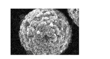
ここで、参考までに、図3に、実施例1に係る絶縁被覆粒子の走査型電子顕微鏡(SEM)による画像を示す。図3Aは中倍率の画像であり、図3Bは高倍率の画像である。
得られた絶縁被覆粒子について、下記の方法(1)~(3)に従って、重合体の平均被覆厚み、被覆率及び固着性の評価を行った。
ガラス容器に、表1に示す量の導電性粒子(積水化学工業株式会社製、「AUL704」)、及び表1に示す量の95%の量の溶媒としてのエタノールを投入した後、撹拌翼を用いて混合し、スラリー液を調製した。このスラリー液に対し、窒素を160mL/分の流量で加えてイナート化を行うとともに、表1に示す重合性単量体を表1に示す量だけ加えた。
重合性単量体を加えた10分後に、表1に示す量の5%の量のエタノールに予め溶解させておいた表1に示す量の反応開始剤(油溶性のアゾ化合物)をスラリー液に投入し、このようにして、重合性単量体、導電性粒子、及び反応開始剤と、溶媒との混合物を調製した。反応開始剤を投入して5分間撹拌した後に、窒素によるイナート化を停止した。
その後、撹拌しながら混合物を70℃に加熱して(即ち、混合物に熱エネルギーを付与して)3時間保持した後、40℃まで徐冷した。これにより、混合物中で、重合性単量体が重合して重合体が形成するとともに、導電性粒子の表面が当該重合体によって被覆された固形分が生成した。徐冷後、15分間静置し、混合物中に分散している固形分を沈降させた。沈降後、デカンテーションにて上澄みを除去し、溶媒を750g加えて15分間撹拌することにより、固形分を洗浄した。
その後、吸引濾過にて固形分を回収し、回収した固形分を、70℃にて12時間乾燥することで、絶縁被覆粒子を得た。
ここで、参考までに、図3に、実施例1に係る絶縁被覆粒子の走査型電子顕微鏡(SEM)による画像を示す。図3Aは中倍率の画像であり、図3Bは高倍率の画像である。
得られた絶縁被覆粒子について、下記の方法(1)~(3)に従って、重合体の平均被覆厚み、被覆率及び固着性の評価を行った。
次に、得られた絶縁被覆粒子30質量部、フェノキシ樹脂(新日鐵化学株式会社製、「YP-50」)60質量部、液状エポキシ樹脂(三菱化学株式会社製、「EP828」)40質量部、エポキシ樹脂用硬化剤(三新化学工業株式会社製、「SI-60L」)3質量部、及びシランカップリング剤(信越化学工業株式会社製、「KBM403」)1質量部を、トルエン中で混合した。この混合物を、バーコーターにより、剥離処理を施したPETフィルム上に塗布した後、70℃で乾燥させてトルエンを揮発させて、厚み20μmの「異方性導電接着フィルム(トルエン使用)」を製造した。
また、上記において、トルエンに代えてメチルエチルケトン(MEK)を用いるとともに、乾燥温度を70℃から50℃に変えたこと以外は、上記と同様のやり方で、厚み20μmの「異方性導電接着フィルム(MEK使用)」を製造した。
得られた異方性導電接着フィルムを用い、下記の方法(4)、(5)に従って、絶縁性及び導通性の評価を行った。
また、上記において、トルエンに代えてメチルエチルケトン(MEK)を用いるとともに、乾燥温度を70℃から50℃に変えたこと以外は、上記と同様のやり方で、厚み20μmの「異方性導電接着フィルム(MEK使用)」を製造した。
得られた異方性導電接着フィルムを用い、下記の方法(4)、(5)に従って、絶縁性及び導通性の評価を行った。
(比較例1)
導電性粒子(積水化学工業株式会社製、「AUL704」)を用意した。そして、実施例1~7において、絶縁被覆粒子に代えてこの導電性粒子を用いたこと以外は、実施例1~7と同様にして、各種評価を行った。
導電性粒子(積水化学工業株式会社製、「AUL704」)を用意した。そして、実施例1~7において、絶縁被覆粒子に代えてこの導電性粒子を用いたこと以外は、実施例1~7と同様にして、各種評価を行った。
(比較例2,3)
導電性粒子の表面を被覆するための重合体として、架橋アクリル樹脂(総研化学株式会社製、商品名:MPシリーズ)を準備した。この架橋アクリル樹脂4gと、導電性粒子(積水化学工業株式会社製、「AUL704」)20gとを、ハイブリダイザー(株式会社奈良機械製作所製、商品名:NHSシリーズ)に導入し、乾式法により、導電性粒子に重合体を被覆させて、被覆粒子を得た。なお、ハイブリダイザーにおける処理条件としては、回転速度16000/分、反応槽温度60℃とし、所望の被覆厚が得られるまでハイブリダイザーを稼動した。
ここで、参考までに、図4に、比較例2に係る被覆粒子の走査型電子顕微鏡(SEM)による画像を示す。図4Aは中倍率の画像であり、図4Bは高倍率の画像である。
そして、実施例1~7において、絶縁被覆粒子に代えてこの被覆粒子を用いたこと以外は、実施例1~7と同様にして、各種評価を行った。
導電性粒子の表面を被覆するための重合体として、架橋アクリル樹脂(総研化学株式会社製、商品名:MPシリーズ)を準備した。この架橋アクリル樹脂4gと、導電性粒子(積水化学工業株式会社製、「AUL704」)20gとを、ハイブリダイザー(株式会社奈良機械製作所製、商品名:NHSシリーズ)に導入し、乾式法により、導電性粒子に重合体を被覆させて、被覆粒子を得た。なお、ハイブリダイザーにおける処理条件としては、回転速度16000/分、反応槽温度60℃とし、所望の被覆厚が得られるまでハイブリダイザーを稼動した。
ここで、参考までに、図4に、比較例2に係る被覆粒子の走査型電子顕微鏡(SEM)による画像を示す。図4Aは中倍率の画像であり、図4Bは高倍率の画像である。
そして、実施例1~7において、絶縁被覆粒子に代えてこの被覆粒子を用いたこと以外は、実施例1~7と同様にして、各種評価を行った。
(評価)
得られた各被覆粒子について、以下の評価を行った。
得られた各被覆粒子について、以下の評価を行った。
(1)重合体の平均被覆厚み
収束イオンビーム(FIB)を用いて各被覆粒子を切断した後、透過型電子顕微鏡(TEM)で断面を観察することにより、被覆されている重合体の平均厚み(重合体の平均被覆厚み)(nm)を測定した。結果を表1に示す。具体的には、TEMで観察される被覆粒子における導電性粒子の表面のうち、重合体が被覆されている箇所について、被覆厚みが最大である箇所及び最小である箇所を含むようにして、平均的な被覆厚みを測定した。そして、2つの被覆粒子サンプルからの平均的な被覆厚みの平均をとったものを採用した。
収束イオンビーム(FIB)を用いて各被覆粒子を切断した後、透過型電子顕微鏡(TEM)で断面を観察することにより、被覆されている重合体の平均厚み(重合体の平均被覆厚み)(nm)を測定した。結果を表1に示す。具体的には、TEMで観察される被覆粒子における導電性粒子の表面のうち、重合体が被覆されている箇所について、被覆厚みが最大である箇所及び最小である箇所を含むようにして、平均的な被覆厚みを測定した。そして、2つの被覆粒子サンプルからの平均的な被覆厚みの平均をとったものを採用した。
(2)重合体の被覆率
収束イオンビーム(FIB)を用いて各被覆粒子を切断した後、透過型電子顕微鏡(TEM)で断面を観察し、各被覆粒子における全表面の面積のうち、重合体が被覆されている表面の面積の割合(%)を、重合体の被覆率として求めた。そして、以下の基準に従い、評価した。結果を表1に示す。
重合体の被覆率が40%超・・・A
重合体の被覆率が25%以上40%以下・・・B
重合体の被覆率が0%超25%未満・・・C
重合体の被覆率が0%・・・D
収束イオンビーム(FIB)を用いて各被覆粒子を切断した後、透過型電子顕微鏡(TEM)で断面を観察し、各被覆粒子における全表面の面積のうち、重合体が被覆されている表面の面積の割合(%)を、重合体の被覆率として求めた。そして、以下の基準に従い、評価した。結果を表1に示す。
重合体の被覆率が40%超・・・A
重合体の被覆率が25%以上40%以下・・・B
重合体の被覆率が0%超25%未満・・・C
重合体の被覆率が0%・・・D
(3)重合体の固着性
各被覆粒子10gを50mlの蒸留水に分散させ、振とうした後、静置した。そして、この液の上澄み液を目視にて確認し、濁っていない場合には〇、濁っている場合には×として評価した。結果を表1に示す。上澄み液が濁っていなければ、導電性粒子の表面を被覆する重合体は、当該表面に固着されていることを示す。
各被覆粒子10gを50mlの蒸留水に分散させ、振とうした後、静置した。そして、この液の上澄み液を目視にて確認し、濁っていない場合には〇、濁っている場合には×として評価した。結果を表1に示す。上澄み液が濁っていなければ、導電性粒子の表面を被覆する重合体は、当該表面に固着されていることを示す。
(4)導通性
導通性評価用に、幅1.8mm×長さ20mm、厚み0.5mmのIC基板を備え、一方の側縁に沿って複数の金メッキバンプが1列ストレート配列で形成されたICを用意した。各バンプは、30μm×85μm、厚みを15μmとした。
また、導通性評価用のガラス基板として、厚み0.7mm、上記ICのバンプと同サイズ同ピッチの電極パターンが形成されたITOパターングラスを用意した。
そして、このガラス基板に異方性導電接着フィルムを仮貼りした後、ICにおけるバンプとガラス基板における電極とより、接続体サンプルを作製した。ここで、熱圧着の条件は、170℃、60MPa、5sec/テフロン(登録商標)50μmとした。
作製した各接続体サンプルについて、85℃、85%RHの条件下で、電流1mAを500h流したときの導通抵抗を測定した。測定値が1.8Ω未満である場合を◎(最良)、1.8Ω以上3Ω未満である場合を○(良好)、3Ω以上5Ω未満である場合を△(普通)、5Ω以上である場合を×(不良)とした。結果を表1に示す。
導通性評価用に、幅1.8mm×長さ20mm、厚み0.5mmのIC基板を備え、一方の側縁に沿って複数の金メッキバンプが1列ストレート配列で形成されたICを用意した。各バンプは、30μm×85μm、厚みを15μmとした。
また、導通性評価用のガラス基板として、厚み0.7mm、上記ICのバンプと同サイズ同ピッチの電極パターンが形成されたITOパターングラスを用意した。
そして、このガラス基板に異方性導電接着フィルムを仮貼りした後、ICにおけるバンプとガラス基板における電極とより、接続体サンプルを作製した。ここで、熱圧着の条件は、170℃、60MPa、5sec/テフロン(登録商標)50μmとした。
作製した各接続体サンプルについて、85℃、85%RHの条件下で、電流1mAを500h流したときの導通抵抗を測定した。測定値が1.8Ω未満である場合を◎(最良)、1.8Ω以上3Ω未満である場合を○(良好)、3Ω以上5Ω未満である場合を△(普通)、5Ω以上である場合を×(不良)とした。結果を表1に示す。
(5)絶縁性
絶縁性評価用に、幅1.5mm×長さ130mm、厚み0.5mmのIC基板を備え、一方の側縁に沿って複数の金メッキバンプが1列ストレート配列で形成されたICを用意した。このICは、各バンプの厚みを15μmとし、バンプ間のスペースを10μmとした。
また、絶縁性評価用のガラス基板として、厚み0.5mm、上記ICのバンプと同サイズ同ピッチの櫛歯状の電極パターンが形成されたITOパターングラスを用意した。
そして、このガラス基板に異方性導電接着フィルムを仮貼りした後、ICにおけるバンプとガラス基板における電極パターンとのアライメントを取りながらICを搭載し、熱圧着ヘッドにより熱圧着することにより、接続体サンプルを作製した。ここで、熱圧着の条件は、170℃、60MPa、5sec/テフロン(登録商標)50μmとした。
作製した各接続体サンプルについて、2端子法にて、隣接するバンプ間の抵抗値を測定した。なお、ICには、10組のバンプからなる電極パターンが8か所形成され、10組中1組以上のショートが発生した電極パターンの数をカウントした。測定した抵抗値が108Ω以下である場合にはショート発生として、ショートが発生した電極パターンの数が0の場合を◎(最良)、ショートが発生した電極パターンが1か所の場合を○(良好)、ショートが発生した電極パターンが2か所の場合を△(普通)、ショートが発生した電極パターンが3か所以上の場合を×(不良)とした。結果を表1に示す。
絶縁性評価用に、幅1.5mm×長さ130mm、厚み0.5mmのIC基板を備え、一方の側縁に沿って複数の金メッキバンプが1列ストレート配列で形成されたICを用意した。このICは、各バンプの厚みを15μmとし、バンプ間のスペースを10μmとした。
また、絶縁性評価用のガラス基板として、厚み0.5mm、上記ICのバンプと同サイズ同ピッチの櫛歯状の電極パターンが形成されたITOパターングラスを用意した。
そして、このガラス基板に異方性導電接着フィルムを仮貼りした後、ICにおけるバンプとガラス基板における電極パターンとのアライメントを取りながらICを搭載し、熱圧着ヘッドにより熱圧着することにより、接続体サンプルを作製した。ここで、熱圧着の条件は、170℃、60MPa、5sec/テフロン(登録商標)50μmとした。
作製した各接続体サンプルについて、2端子法にて、隣接するバンプ間の抵抗値を測定した。なお、ICには、10組のバンプからなる電極パターンが8か所形成され、10組中1組以上のショートが発生した電極パターンの数をカウントした。測定した抵抗値が108Ω以下である場合にはショート発生として、ショートが発生した電極パターンの数が0の場合を◎(最良)、ショートが発生した電極パターンが1か所の場合を○(良好)、ショートが発生した電極パターンが2か所の場合を△(普通)、ショートが発生した電極パターンが3か所以上の場合を×(不良)とした。結果を表1に示す。
*1 導電性粒子:積水化学工業株式会社製、「AUL704」
*2 ジビニルベンゼン:和光純薬工業株式会社製
*3 (メタ)アクリレート化合物A:1.6-ヘキサンジオールジメタクリレート、共栄社化学株式会社製、「ライトエステル1.6HX」
*4 (メタ)アクリレート化合物B:エチレングリコールジメタクリレート、共栄社化学株式会社製、「ライトエステルEG」
*5 反応開始剤:2,2’-アゾビス(2,4-ジメチルバレロニトリル)、和光純薬工業株式会社製、「V-65」
*2 ジビニルベンゼン:和光純薬工業株式会社製
*3 (メタ)アクリレート化合物A:1.6-ヘキサンジオールジメタクリレート、共栄社化学株式会社製、「ライトエステル1.6HX」
*4 (メタ)アクリレート化合物B:エチレングリコールジメタクリレート、共栄社化学株式会社製、「ライトエステルEG」
*5 反応開始剤:2,2’-アゾビス(2,4-ジメチルバレロニトリル)、和光純薬工業株式会社製、「V-65」
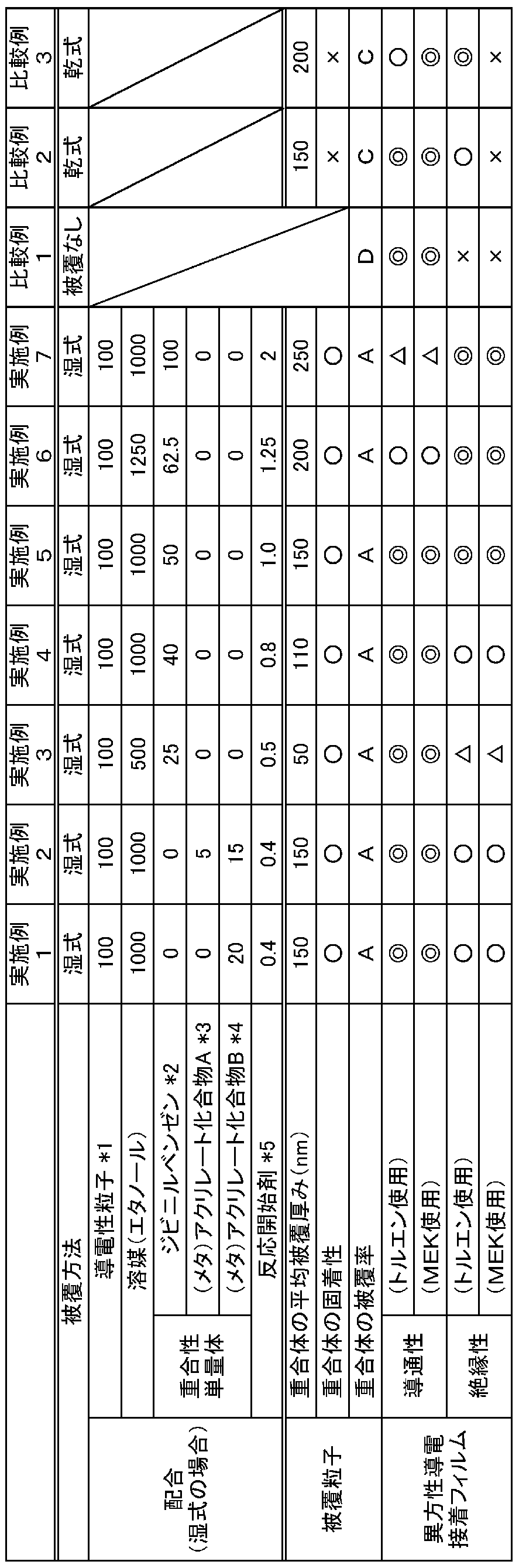
表1より、導電性粒子の表面の少なくとも一部に絶縁性重合体が固着されている絶縁被覆粒子を用いた実施例1~7では、導通性及び絶縁性の両方に優れることが分かる。なお、図3から、実施例に係る絶縁被覆粒子は、導電性粒子の表面の少なくとも一部に絶縁性重合体が強固に付着していることが分かる。
これに対して、絶縁性重合体が被覆されていない粒子を用いた比較例1では、少なくとも絶縁性に劣ることが分かる。
また、従来の乾式法により導電性粒子の表面に重合体を被覆して得られた被覆粒子を用いた比較例2,3では、少なくとも絶縁性に劣ることが分かる。これは、図4、特に図4Aを参照すれば明らかな通り、導電性粒子の表面に重合体を強固に付着させることができていない上、被覆された重合体が異方性導電接着フィルムの調製に用いた溶剤に侵食されたことなどによるものであると考えられる。
これに対して、絶縁性重合体が被覆されていない粒子を用いた比較例1では、少なくとも絶縁性に劣ることが分かる。
また、従来の乾式法により導電性粒子の表面に重合体を被覆して得られた被覆粒子を用いた比較例2,3では、少なくとも絶縁性に劣ることが分かる。これは、図4、特に図4Aを参照すれば明らかな通り、導電性粒子の表面に重合体を強固に付着させることができていない上、被覆された重合体が異方性導電接着フィルムの調製に用いた溶剤に侵食されたことなどによるものであると考えられる。
本発明によれば、複数の端子を備える回路基板同士を電気的に接続させた場合に、各基板上で隣接する端子間の絶縁性を十分に確保しつつ、対向する端子間に導通性をもたらす異方性導電接着剤を得ることが可能な、絶縁被覆粒子、並びに、当該絶縁被覆粒子を含む、粒子含有組成物及び異方性導電接着剤を提供することできる。また、本発明によれば、上述した絶縁被覆粒子を効率的に製造することが可能な、絶縁被覆粒子の製造方法を提供することができる。
Claims (11)
- 導電性粒子の表面の少なくとも一部に、重合性単量体に由来する構造単位を含む絶縁性重合体が固着されていることを特徴とする、絶縁被覆粒子。
- 前記絶縁性重合体の被覆率が40%超である、請求項1に記載の絶縁被覆粒子。
- 前記重合性単量体が、2つ以上の重合性官能基を有する単量体を含む、請求項1又は2に記載の絶縁被覆粒子。
- 前記2つ以上の重合性官能基を有する単量体が、ジビニルベンゼンである、請求項3に記載の絶縁被覆粒子。
- 前記2つ以上の重合性官能基を有する単量体が、(メタ)アクリレート化合物である、請求項3に記載の絶縁被覆粒子。
- 前記絶縁性重合体の平均被覆厚みが、50nm以上である、請求項1~5のいずれかに記載の絶縁被覆粒子。
- 重合性単量体、導電性粒子、及び反応開始剤と、溶媒との混合物を調製する工程と、
前記混合物を撹拌しながら該混合物にエネルギーを付与することにより、前記重合性単量体が重合されてなる絶縁性重合体を生成するとともに、前記導電性粒子の表面の少なくとも一部に、前記絶縁性重合体を固着させる工程と、
を含むことを特徴とする、絶縁被覆粒子の製造方法。 - 前記溶媒は、前記重合性単量体を溶解するが、前記絶縁性重合体を溶解しない溶媒である、請求項7に記載の絶縁被覆粒子の製造方法。
- 前記エネルギーが熱エネルギーである、請求項7又は8に記載の絶縁被覆粒子の製造方法。
- 請求項1~6のいずれかに記載の絶縁被覆粒子を含むことを特徴とする、粒子含有組成物。
- 請求項10に記載の粒子含有組成物を含むことを特徴とする、異方性導電接着剤。
Priority Applications (3)
| Application Number | Priority Date | Filing Date | Title |
|---|---|---|---|
| KR1020187033467A KR20180135951A (ko) | 2016-07-07 | 2017-07-05 | 절연 피복 입자, 절연 피복 입자의 제조 방법, 입자 함유 조성물, 및 이방성 도전 접착제 |
| CN201780038784.9A CN109313952B (zh) | 2016-07-07 | 2017-07-05 | 绝缘被覆粒子、绝缘被覆粒子的制造方法、含有粒子的组合物和各向异性导电粘接剂 |
| KR1020207033007A KR102345705B1 (ko) | 2016-07-07 | 2017-07-05 | 절연 피복 입자, 절연 피복 입자의 제조 방법, 입자 함유 조성물, 및 이방성 도전 접착제 |
Applications Claiming Priority (2)
| Application Number | Priority Date | Filing Date | Title |
|---|---|---|---|
| JP2016-135394 | 2016-07-07 | ||
| JP2016135394A JP6893399B2 (ja) | 2016-07-07 | 2016-07-07 | 絶縁被覆粒子、絶縁被覆粒子の製造方法、粒子含有組成物、及び異方性導電接着剤 |
Publications (1)
| Publication Number | Publication Date |
|---|---|
| WO2018008693A1 true WO2018008693A1 (ja) | 2018-01-11 |
Family
ID=60912861
Family Applications (1)
| Application Number | Title | Priority Date | Filing Date |
|---|---|---|---|
| PCT/JP2017/024693 Ceased WO2018008693A1 (ja) | 2016-07-07 | 2017-07-05 | 絶縁被覆粒子、絶縁被覆粒子の製造方法、粒子含有組成物、及び異方性導電接着剤 |
Country Status (4)
| Country | Link |
|---|---|
| JP (1) | JP6893399B2 (ja) |
| KR (2) | KR102345705B1 (ja) |
| CN (1) | CN109313952B (ja) |
| WO (1) | WO2018008693A1 (ja) |
Citations (5)
| Publication number | Priority date | Publication date | Assignee | Title |
|---|---|---|---|---|
| JPH04362104A (ja) * | 1991-06-07 | 1992-12-15 | Fujitsu Ltd | 金属微粒子のポリマ被覆方法 |
| JP2007537572A (ja) * | 2004-05-12 | 2007-12-20 | マイクログローブ コープ カンパニー リミテッド | 異方性導電接続用の絶縁導電性粒子及びその製造方法並びにこれを用いた異方性導電接続材料 |
| JP2007537570A (ja) * | 2004-05-12 | 2007-12-20 | チェイル インダストリーズ インコーポレイテッド | 絶縁導電性微粒子及びこれを含有する異方導電性接着フィルム |
| WO2012124724A1 (ja) * | 2011-03-16 | 2012-09-20 | ソニーケミカル&インフォメーションデバイス株式会社 | 光反射性異方性導電接着剤及び発光装置 |
| JP2014017213A (ja) * | 2012-07-11 | 2014-01-30 | Hitachi Chemical Co Ltd | 絶縁被覆導電粒子及びそれを用いた異方導電性接着剤 |
Family Cites Families (7)
| Publication number | Priority date | Publication date | Assignee | Title |
|---|---|---|---|---|
| JP2794009B2 (ja) | 1996-01-29 | 1998-09-03 | 富士ゼロックス株式会社 | 電気接続用異方導電性粒子の製造方法および電気接続用異方導電材料の製造方法 |
| KR100722493B1 (ko) * | 2005-09-02 | 2007-05-28 | 제일모직주식회사 | 절연 전도성 미립자 및 이를 이용한 이방 전도성 접착필름 |
| JP4967482B2 (ja) | 2006-02-27 | 2012-07-04 | 日立化成工業株式会社 | 導電粒子、接着剤組成物及び回路接続材料 |
| JP5834548B2 (ja) * | 2011-07-04 | 2015-12-24 | 日立化成株式会社 | 絶縁被覆導電粒子及び異方導電性接着フィルム |
| JP6044195B2 (ja) * | 2011-09-06 | 2016-12-14 | 日立化成株式会社 | 絶縁被覆用粒子、絶縁被覆導電粒子、異方導電材料及び接続構造体 |
| KR101534841B1 (ko) * | 2012-11-07 | 2015-07-07 | 제일모직주식회사 | 돌기형 도전성 미립자 및 이를 포함하는 이방 도전성 필름 |
| JP6212369B2 (ja) * | 2012-12-05 | 2017-10-11 | 積水化学工業株式会社 | 絶縁性粒子付き導電性粒子、絶縁性粒子付き導電性粒子の製造方法、導電材料及び接続構造体 |
-
2016
- 2016-07-07 JP JP2016135394A patent/JP6893399B2/ja active Active
-
2017
- 2017-07-05 KR KR1020207033007A patent/KR102345705B1/ko active Active
- 2017-07-05 KR KR1020187033467A patent/KR20180135951A/ko not_active Ceased
- 2017-07-05 CN CN201780038784.9A patent/CN109313952B/zh active Active
- 2017-07-05 WO PCT/JP2017/024693 patent/WO2018008693A1/ja not_active Ceased
Patent Citations (5)
| Publication number | Priority date | Publication date | Assignee | Title |
|---|---|---|---|---|
| JPH04362104A (ja) * | 1991-06-07 | 1992-12-15 | Fujitsu Ltd | 金属微粒子のポリマ被覆方法 |
| JP2007537572A (ja) * | 2004-05-12 | 2007-12-20 | マイクログローブ コープ カンパニー リミテッド | 異方性導電接続用の絶縁導電性粒子及びその製造方法並びにこれを用いた異方性導電接続材料 |
| JP2007537570A (ja) * | 2004-05-12 | 2007-12-20 | チェイル インダストリーズ インコーポレイテッド | 絶縁導電性微粒子及びこれを含有する異方導電性接着フィルム |
| WO2012124724A1 (ja) * | 2011-03-16 | 2012-09-20 | ソニーケミカル&インフォメーションデバイス株式会社 | 光反射性異方性導電接着剤及び発光装置 |
| JP2014017213A (ja) * | 2012-07-11 | 2014-01-30 | Hitachi Chemical Co Ltd | 絶縁被覆導電粒子及びそれを用いた異方導電性接着剤 |
Also Published As
| Publication number | Publication date |
|---|---|
| JP6893399B2 (ja) | 2021-06-23 |
| CN109313952B (zh) | 2021-10-19 |
| JP2018006278A (ja) | 2018-01-11 |
| KR20180135951A (ko) | 2018-12-21 |
| CN109313952A (zh) | 2019-02-05 |
| KR20200131359A (ko) | 2020-11-23 |
| KR102345705B1 (ko) | 2021-12-30 |
Similar Documents
| Publication | Publication Date | Title |
|---|---|---|
| KR100710103B1 (ko) | 피복 도전성 미립자, 피복 도전성 미립자의 제조방법,이방성 도전재료, 및 도전 접속 구조체 | |
| JP6475805B2 (ja) | 絶縁性粒子付き導電性粒子、導電材料及び接続構造体 | |
| JP5054232B2 (ja) | 導電性粒子、異方性導電材料及び接続構造体 | |
| JP6188456B2 (ja) | 絶縁性粒子付き導電性粒子、導電材料及び接続構造体 | |
| WO2012014925A1 (ja) | 絶縁性粒子付き導電性粒子、絶縁性粒子付き導電性粒子の製造方法、異方性導電材料及び接続構造体 | |
| JP6084850B2 (ja) | 絶縁性粒子付き導電性粒子、導電材料及び接続構造体 | |
| JP6165626B2 (ja) | 導電性粒子、導電材料及び接続構造体 | |
| JP6577698B2 (ja) | 導電フィルム及び接続構造体 | |
| JPWO2019194135A1 (ja) | 絶縁性粒子付き導電性粒子、導電材料及び接続構造体 | |
| JP6246242B2 (ja) | 絶縁被覆炭素繊維、絶縁被覆炭素繊維の製造方法、炭素繊維含有組成物及び熱伝導性シート | |
| CN1820328A (zh) | 用于各向异性导电连接的绝缘导电球及其制备方法和制品 | |
| JP2022022293A (ja) | 導電性粒子、導電材料及び接続構造体 | |
| JP5530571B1 (ja) | 絶縁性粒子付き導電性粒子、導電材料及び接続構造体 | |
| JP6151990B2 (ja) | 絶縁性粒子付き導電性粒子、導電材料及び接続構造体 | |
| JP2007537572A (ja) | 異方性導電接続用の絶縁導電性粒子及びその製造方法並びにこれを用いた異方性導電接続材料 | |
| JP6893399B2 (ja) | 絶縁被覆粒子、絶縁被覆粒子の製造方法、粒子含有組成物、及び異方性導電接着剤 | |
| JP7180981B2 (ja) | 導電性粒子、導電材料及び接続構造体 | |
| JP2016154139A (ja) | 導電性粒子粉体、導電性粒子粉体の製造方法、導電材料及び接続構造体 | |
| JP6592235B2 (ja) | 絶縁性粒子付き導電性粒子、絶縁性粒子付き導電性粒子の製造方法、導電材料及び接続構造体 | |
| HK40001203A (zh) | 绝缘被覆粒子、绝缘被覆粒子的制造方法、含有粒子的组合物和各向异性导电粘接剂 | |
| JP2022008631A (ja) | 導電性粒子、導電性粒子の製造方法、導電材料及び接続構造体 | |
| WO2017026428A1 (ja) | 絶縁被覆炭素繊維、絶縁被覆炭素繊維の製造方法、炭素繊維含有組成物及び熱伝導性シート | |
| JP6145004B2 (ja) | 接続構造体の製造方法、bステージ化された異方性導電材料及び接続構造体 | |
| JP7271543B2 (ja) | 絶縁性粒子付き導電性粒子、導電材料及び接続構造体 | |
| JPWO2019194133A1 (ja) | 絶縁性粒子付き導電性粒子、絶縁性粒子付き導電性粒子の製造方法、導電材料及び接続構造体 |
Legal Events
| Date | Code | Title | Description |
|---|---|---|---|
| DPE1 | Request for preliminary examination filed after expiration of 19th month from priority date (pct application filed from 20040101) | ||
| ENP | Entry into the national phase |
Ref document number: 20187033467 Country of ref document: KR Kind code of ref document: A |
|
| 121 | Ep: the epo has been informed by wipo that ep was designated in this application |
Ref document number: 17824296 Country of ref document: EP Kind code of ref document: A1 |
|
| NENP | Non-entry into the national phase |
Ref country code: DE |
|
| 122 | Ep: pct application non-entry in european phase |
Ref document number: 17824296 Country of ref document: EP Kind code of ref document: A1 |