WO2018004152A1 - 후처리 후 에칭성이 우수한 표면처리동박 및 그 제조방법 - Google Patents
후처리 후 에칭성이 우수한 표면처리동박 및 그 제조방법 Download PDFInfo
- Publication number
- WO2018004152A1 WO2018004152A1 PCT/KR2017/006095 KR2017006095W WO2018004152A1 WO 2018004152 A1 WO2018004152 A1 WO 2018004152A1 KR 2017006095 W KR2017006095 W KR 2017006095W WO 2018004152 A1 WO2018004152 A1 WO 2018004152A1
- Authority
- WO
- WIPO (PCT)
- Prior art keywords
- copper foil
- roughening
- nodule
- width
- ions
- Prior art date
Links
Images

Classifications
-
- C—CHEMISTRY; METALLURGY
- C25—ELECTROLYTIC OR ELECTROPHORETIC PROCESSES; APPARATUS THEREFOR
- C25D—PROCESSES FOR THE ELECTROLYTIC OR ELECTROPHORETIC PRODUCTION OF COATINGS; ELECTROFORMING; APPARATUS THEREFOR
- C25D5/00—Electroplating characterised by the process; Pretreatment or after-treatment of workpieces
- C25D5/60—Electroplating characterised by the structure or texture of the layers
- C25D5/605—Surface topography of the layers, e.g. rough, dendritic or nodular layers
-
- C—CHEMISTRY; METALLURGY
- C23—COATING METALLIC MATERIAL; COATING MATERIAL WITH METALLIC MATERIAL; CHEMICAL SURFACE TREATMENT; DIFFUSION TREATMENT OF METALLIC MATERIAL; COATING BY VACUUM EVAPORATION, BY SPUTTERING, BY ION IMPLANTATION OR BY CHEMICAL VAPOUR DEPOSITION, IN GENERAL; INHIBITING CORROSION OF METALLIC MATERIAL OR INCRUSTATION IN GENERAL
- C23G—CLEANING OR DE-GREASING OF METALLIC MATERIAL BY CHEMICAL METHODS OTHER THAN ELECTROLYSIS
- C23G1/00—Cleaning or pickling metallic material with solutions or molten salts
- C23G1/02—Cleaning or pickling metallic material with solutions or molten salts with acid solutions
- C23G1/10—Other heavy metals
-
- C—CHEMISTRY; METALLURGY
- C25—ELECTROLYTIC OR ELECTROPHORETIC PROCESSES; APPARATUS THEREFOR
- C25D—PROCESSES FOR THE ELECTROLYTIC OR ELECTROPHORETIC PRODUCTION OF COATINGS; ELECTROFORMING; APPARATUS THEREFOR
- C25D3/00—Electroplating: Baths therefor
- C25D3/02—Electroplating: Baths therefor from solutions
- C25D3/38—Electroplating: Baths therefor from solutions of copper
-
- C—CHEMISTRY; METALLURGY
- C25—ELECTROLYTIC OR ELECTROPHORETIC PROCESSES; APPARATUS THEREFOR
- C25D—PROCESSES FOR THE ELECTROLYTIC OR ELECTROPHORETIC PRODUCTION OF COATINGS; ELECTROFORMING; APPARATUS THEREFOR
- C25D3/00—Electroplating: Baths therefor
- C25D3/02—Electroplating: Baths therefor from solutions
- C25D3/56—Electroplating: Baths therefor from solutions of alloys
-
- C—CHEMISTRY; METALLURGY
- C25—ELECTROLYTIC OR ELECTROPHORETIC PROCESSES; APPARATUS THEREFOR
- C25D—PROCESSES FOR THE ELECTROLYTIC OR ELECTROPHORETIC PRODUCTION OF COATINGS; ELECTROFORMING; APPARATUS THEREFOR
- C25D5/00—Electroplating characterised by the process; Pretreatment or after-treatment of workpieces
- C25D5/10—Electroplating with more than one layer of the same or of different metals
-
- H—ELECTRICITY
- H05—ELECTRIC TECHNIQUES NOT OTHERWISE PROVIDED FOR
- H05K—PRINTED CIRCUITS; CASINGS OR CONSTRUCTIONAL DETAILS OF ELECTRIC APPARATUS; MANUFACTURE OF ASSEMBLAGES OF ELECTRICAL COMPONENTS
- H05K1/00—Printed circuits
- H05K1/02—Details
- H05K1/09—Use of materials for the conductive, e.g. metallic pattern
-
- H—ELECTRICITY
- H05—ELECTRIC TECHNIQUES NOT OTHERWISE PROVIDED FOR
- H05K—PRINTED CIRCUITS; CASINGS OR CONSTRUCTIONAL DETAILS OF ELECTRIC APPARATUS; MANUFACTURE OF ASSEMBLAGES OF ELECTRICAL COMPONENTS
- H05K3/00—Apparatus or processes for manufacturing printed circuits
- H05K3/02—Apparatus or processes for manufacturing printed circuits in which the conductive material is applied to the surface of the insulating support and is thereafter removed from such areas of the surface which are not intended for current conducting or shielding
- H05K3/022—Processes for manufacturing precursors of printed circuits, i.e. copper-clad substrates
- H05K3/025—Processes for manufacturing precursors of printed circuits, i.e. copper-clad substrates by transfer of thin metal foil formed on a temporary carrier, e.g. peel-apart copper
-
- H—ELECTRICITY
- H05—ELECTRIC TECHNIQUES NOT OTHERWISE PROVIDED FOR
- H05K—PRINTED CIRCUITS; CASINGS OR CONSTRUCTIONAL DETAILS OF ELECTRIC APPARATUS; MANUFACTURE OF ASSEMBLAGES OF ELECTRICAL COMPONENTS
- H05K2201/00—Indexing scheme relating to printed circuits covered by H05K1/00
- H05K2201/03—Conductive materials
- H05K2201/0332—Structure of the conductor
- H05K2201/0335—Layered conductors or foils
- H05K2201/0355—Metal foils
Definitions
- the present invention relates to a surface-treated copper foil for a microcircuit board and a method for manufacturing the same. More particularly, the surface-treated copper foil for a microcircuit board having an excellent etching property suitable for fine pitch formation due to its good etching property in forming a circuit pattern and It relates to a manufacturing method.
- the printed circuit board is manufactured by attaching an insulating substrate to the copper foil to form a laminate, and then forming a conductor pattern on the copper foil surface by etching. In such an etching process, as the width of the printed circuit board is gradually reduced, the etching must be uniformly performed according to the designed width of the circuit.
- the copper foil As the most basic characteristic required for such a copper foil, it is required to have excellent adhesive strength between the copper foil and the insulating base substrate.
- the copper foil must maintain the adhesive strength above the required characteristics not only immediately after heating and pressing and laminating with an insulating substrate, but also after various treatments in subsequent post-processing steps. To this end, the chemical resistance, heat resistance, and the like to acids, alkalis, and the like should be excellent.
- the etching residual material it is required that the etching residual material be excellent in etching property such as not remaining in the non-pattern portion.
- the process of increasing the surface area of a copper foil surface is normally used by performing what is called roughening process which precipitates fine copper particle on the copper foil surface.
- the surface roughness Rz is high, thereby inferior in the uniformity of the circuit width. That is, the problem may arise that the Rz of the provided copper foil is high and the circuit width after the etching is not uniform and a portion which is not etched remains.
- the printed circuit board considering the high frequency characteristics, since the process proceeds within 1 to 2 ⁇ m from the surface, when the surface roughness is increased through overtreatment, an interference factor of signal transmission increases.
- the copper part of the copper foil circuit after etching will be etched in the shape which spreads downward from the surface of copper foil toward a numerical layer. This phenomenon is called sag phenomenon. When a large sag occurs, defective products may occur such as uncirculated copper remaining near the resin substrate and a short circuit.
- the present invention provides a surface-treated copper foil for a microcircuit board and a method of manufacturing the same for improving the etching property so as to minimize the deflection phenomenon evenly in accordance with the designed circuit width during circuit etching in accordance with the trend of decreasing the circuit width.
- the roughening step may be performed for 2.7 to 3.3 seconds at a current density of 45 to 55A / dm 2 .
- the roughening step may be performed in a plating bath containing molybdenum (Mo) 0.5 ⁇ 3g / l, tungsten ion (W) 0.1 ⁇ 0.5g / l.
- the cover plating layer forming step 2.7 to 3.3 at a current density of 14 to 16 A / dm 2 in a plating solution formed at a concentration of 100 to 200 g / L copper and 100 to 200 g / L sulfuric acid on the nodule grown through the roughening treatment. Secondary plating can be performed.
- the method may further include pickling the electrolytic copper foil provided above.
- the surface treatment copper foil for a microcircuit board according to the present invention is a combination of the copper foil and one surface of the copper foil to form a nodule And a roughened layer, wherein the grown nodule height is 1.0 to 3.0 mu m, and a difference between a lower width and an upper width of a circuit pattern formed after etching is within 10 mu m.
- the surface roughness Rz of the roughened layer may be 1.5 to 2.0 ⁇ m or less.
- the surface roughness Rz is 2.0 or less and the etching property is good, so that the sagging phenomenon is not large, that is, the difference between the width of the lower circuit and the width of the upper circuit in the vicinity of the resin layer is 10 ⁇ m or less. Can be.
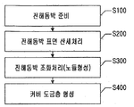
- FIG. 1 is a flowchart illustrating a method of manufacturing a surface-treated copper foil for a microcircuit board according to an embodiment of the present invention.
- FIG. 2 is a SEM photograph showing the surface of the surface-treated copper foil according to the present invention.
- FIG. 3 is a SEM photograph showing a cross section of the surface-treated copper foil according to the present invention.
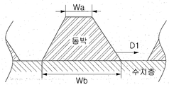
- FIG. 4 is a schematic diagram for explaining the concept of the width of the upper and lower circuits.
- Surface-treated copper foil for a microcircuit board manufactured according to the present invention has the following characteristics.
- the surface roughness Rz of the surface-treated copper foil after roughening process is 1.5-2.0 micrometers, and the height of the nodule adhering to one surface of copper foil after growth of a nodule is 1.0-3.0 micrometers. Further, the difference between the lower and upper circuit widths after etching is formed to be 10 m or less.
- the etching time is shortened due to the small size of the nodule, and the length and bottom of the top of the circuit designed after etching due to the shortened etching time (bottom; one surface near the resin layer) is reduced in length difference.
- the height of the nodule described in the present invention refers to the distance between the copper foil surface and the apex of the nodule, and the height of the nodule formed on the roughened electrolytic copper foil surface is preferably in the range of 1.0 ⁇ m to 3.0 ⁇ m.
- the nodule is formed on the surface of the electrolytic copper foil, and when the height of the nodule is less than 1.0 ⁇ m, the height of the nodule to be joined with the resin is low, which is not preferable because the adhesive strength is not excellent. If the height of the nodule exceeds 3.0 ⁇ m, the surface roughness variation of the surface of the electrodeposited copper foil increases, which is not preferable because it can not maintain a stable adhesive strength and lowers the high frequency characteristics.
- an electrolytic copper foil of 12 ⁇ m is prepared (S100).
- a circulating electrolytic cell system was used, and a copper electrolyte having a composition of CuSO 4 ⁇ 5H 2 O 250 to 400 g / L and H 2 SO 4 80 to 150 g / L used for copper foil was used. And additives may be added.
- the thickness of the electrolytic copper foil was 12 micrometers.
- the surface of the electrolytic copper foil is pickled.
- the process of pickling the surface of the electrolytic copper foil of the second step (S200) is a step for cleaning the copper foil by removing impurities from the surface of the copper foil. In the present invention, it is preferable to clean the copper foil through pickling treatment.
- the method of pickling the surface of the electrolytic copper foil is not particularly limited as long as it is known in the art, but non-limiting examples may selectively use degreasing and polishing.
- the degreasing is to remove residues present in the copper foil, and alkali degreasing, acid degreasing or electrolytic degreasing can be applied.
- the electrolytic copper foil cleaned by pickling for the preparation of the surface-treated copper foil for a microcircuit board according to the present invention is treated to form a nodule under the following conditions.
- the coordination process is performed as follows.
- a nodule is formed by roughening the pickled electrolytic copper foil in a plating bath containing 10-20 g / l of copper ions (Cu) and 100-00 g / L of sulfuric acid (H 2 SO 4 ).
- a roughening treatment is performed at a current density of 45 to 55 A / dm 2 for 2.7 to 3.3 seconds, preferably at a current density of 50 A / dm 2 for about 3 seconds.
- the electrolytic copper foil roughened in the third step S300 is formed with a nodule on its surface.
- the surface area of the electrolytic copper foil is increased, thereby increasing the adhesive strength of the nodule.
- the surface roughness of the roughened electrolytic copper foil according to the present invention is 2.0 or less, and more preferably the surface roughness of the roughened electrolytic copper foil according to the present invention has a range of 1.5 to 2.0 ⁇ m.
- the height of the nodule formed on the surface of the electrolytic copper foil subjected to the roughening process in the third step (S300) is preferably in the range of 1.0 ⁇ m to 3.0 ⁇ m.
- the height of the nodule described in the present invention refers to the distance between the copper foil surface and the peak of the nodule.
- the height of the nodule is less than 1.0 ⁇ m, the height of the nodule to be joined with the resin is low, which is not preferable because the adhesive strength is not excellent. If the height of the nodule exceeds 3.0 ⁇ m, the surface roughness variation of the surface of the electrodeposited copper foil increases, which is not preferable because it can not maintain a stable adhesive strength and lowers the high frequency characteristics.
- the cover plating layer is formed by plating for 2.7 to 3.3 seconds, preferably 3 seconds at dm 2 , preferably 15 A / dm 2 .
- the cover plated layer may be formed on the top of the nodule to prevent dropping of the nodule and to improve heat resistance and conductivity.
- Figure 2 shows a photo of the copper foil produced through the formation of the nodule and the cover plating layer as described above. That is, it can be seen that the nodule is formed as shown in FIG. 2 through the surface treatment as described above.
- FIG. 3 is a SEM photograph showing the cross-sectional view of the nodule formed on the surface of the electrolytic copper foil of the surface-treated copper foil according to the present invention. As shown in FIG. 3, it can be seen that nodules are formed on the mat side of the electrolytic copper foil.
- Example 1 molybdenum, tungsten ions, copper ions, and sulfuric acid were added to the plating solution during the roughening treatment of the electrolytic copper foil. Other than that was performed under the same conditions as the above-mentioned manufacturing method. That is, the roughening treatment was performed for 3 seconds at a current density of 50 A / dm 2 under each plating bath condition.
- Example 1 is a plating bath containing 1 g / l molybdenum (Mo), 0.3 g / l tungsten ion (W), 15 g / l copper ion (Cu) and 150 g / L sulfuric acid (H 2 SO 4 ) Was performed in.
- Mo molybdenum
- W 0.3 g / l tungsten ion
- Cu 15 g / l copper ion
- H 2 SO 4 sulfuric acid
- Example 2 roughening was performed by replacing tungsten ions with vanadium ions. That is, it was performed in a plating bath containing 1 g / l of molybdenum (Mo), 0.5 g / l of vanadium ions (V), 15 g / l of copper ions (Cu), and 150 g / L of sulfuric acid (H 2 SO 4 ), The conditions other than this are the same as that of Example 1.
- Mo molybdenum
- V vanadium ions
- Cu 15 g / l of copper ions
- H 2 SO 4 sulfuric acid
- Example 3 was carried out by replacing molybdenum with sodium ions compared to Example 1. That is, it was performed under a plating bath containing 5 g / L sodium ion (Na), 0.3 g / l tungsten ion (W), 15 g / l copper ion (Cu), and 150 g / L sulfuric acid (H 2 SO 4 ). The conditions other than this are the same as that of Example 1.
- Comparative Example 1 is roughened in a plating bath containing 4 g / l molybdenum (Mo), 0.3 g / l tungsten ion (W), 15 g / l copper ion (Cu), and 150 g / L sulfuric acid (H 2 SO 4 ) Treatment was carried out. The conditions other than this are the same as that of Example 1.
- Example 2 the roughening treatment was performed in the plating bath conditions of Example 1 except for molybdenum. That is, the roughening treatment was performed in a plating bath containing 0.3 g / l of tungsten ions (W), 15 g / l of copper ions (Cu), and 150 g / L of sulfuric acid (H 2 SO 4 ). The conditions other than this are the same as that of Example 1.
- Harmonization treatment was carried out under plating solution conditions according to the conditions of the respective examples and comparative examples, and the processed copper foil was implemented to have a circuit width of 30/30 through copper chloride corrosion.
- FIG. 4 is a schematic diagram for explaining the concept of the width of the upper and lower circuits. As shown in FIG. 4, the larger the difference between the lower width Wb of the circuit pattern and the upper width Wa of the circuit pattern that is closer to the numerical layer, the more sag occurs. When the etching property is poor, as described above, a short circuit may occur when the lower portion of the circuit pattern is close to another adjacent circuit pattern.
- Table 1 shows the difference between the width of the upper circuit pattern and the width of the lower circuit pattern.
- the width Wa of the upper circuit was formed to be 21.1 ⁇ m, and the difference from the width Wb of the lower circuit was 8.7 ⁇ m, which was measured to be 10 ⁇ m or less.
- the upper circuit width Wa was formed to be 18.8 and 17.6 mu m, so that the difference from the lower circuit width Wb was 11.6 and 12.8 mu m, respectively, and was 10 mu m or more.
- Mo molybdenum
- W tungsten ion
- Cu copper ion
- the difference between the width of the upper circuit and the lower circuit tended to be measured to be 10 to 13 ⁇ m or more.
- the width of the upper circuit and the lower circuit The difference tended to be very large above 12 ⁇ m.
Landscapes
- Chemical & Material Sciences (AREA)
- Engineering & Computer Science (AREA)
- Metallurgy (AREA)
- Chemical Kinetics & Catalysis (AREA)
- Materials Engineering (AREA)
- Organic Chemistry (AREA)
- Electrochemistry (AREA)
- Microelectronics & Electronic Packaging (AREA)
- General Chemical & Material Sciences (AREA)
- Mechanical Engineering (AREA)
- Manufacturing & Machinery (AREA)
- Electroplating Methods And Accessories (AREA)
- Manufacturing Of Printed Wiring (AREA)
Abstract
본 발명은 미세회로기판용 표면처리동박 및 그의 제조방법에 관한 것으로서, 구체적으로 본 발명에 따른 미세회로기판용 동박의 표면처리 방법은, 전해동박을 제공하는 단계; 및 상기 전해동박 상에 노듈을 성장시키기 위하여 조화처리를 하는 단계;를 포함하고, 상기 조화처리 단계에서는 [몰리브덴(Mo) 0.5 ~ 3g/l 와 나트륨 이온(Na) 1 ~ 10g/l] 중 1종, [텅스텐 이온(W) 0.1 ~ 0.5g/l 와 바나듐 이온(V) 0.3 ~ 0.7 g/l] 중 1종, 구리이온(Cu) 10 ~ 20 g/l 및 황산(H2SO4) 100~00g/L 을 포함하는 도금욕에서 조화처리를 수행한다. 본 발명에 따르면 표면조도 Rz가 2.0 이하이고 에칭성이 좋아 처짐현상이 크지 않은, 즉 수지층 부근의 하부회로의 폭과 상부 회로폭의 차이가 10㎛ 이하인 미세회로기판용 표면처리동박을 제조할 수 있다.
Description
본 발명은 미세회로기판용 표면처리동박 및 그의 제조방법에 관한 것으로서, 보다 상세하게는 회로 패턴 형성시의 에칭성이 양호하여 파인 피치화에 적합한 에칭성이 우수한 미세회로기판용 표면처리동박과 그의 제조방법에 관한 것이다.
최근 전기/전자기기의 소형화, 경량화가 가속화됨에 따라 기판 상에 형성된 인쇄회로가 미세화, 고집적, 소형화되고 있으며, 이에 따라 인쇄회로기판에 사용되는 동박도 다양한 물성이 요구되고 있다.
인쇄회로기판은 동박에 절연 기판을 접착시켜 적층체로 제조한 후에, 에칭에 의하여 동박면에 도체 패턴을 형성하는 공정을 통하여 제조된다. 이러한 에칭 공정에서는 인쇄회로 기판에서 회로폭이 점점 줄어듦에 따라 회로 에칭 시 설계된 회로폭에 맞추어 균일한 에칭이 이루어지도록 해야 한다.
이러한 동박에 요구되는 가장 기본적인 특성으로서, 동박과 절연기재 기판간의 접착강도가 우수할 것이 요구된다. 특히, 동박은 절연기재와 가열 가압하고 적층한 직후 뿐 아니라, 이후의 후처리공정에서의 다양한 처리를 거친 후에도 접착강도를 요구특성 이상으로 유지해야만 한다. 그러기 위해서는, 산이나 알칼리 등에 대한 내약품성, 내열성 등이 우수해야 한다. 또한, 동 회로패턴을 형성하여 프린트 배선판으로 하기 위한 에칭과정에 있어서, 에칭 잔류물질이 비(非)패턴부분에 잔류하지 않는 등 에칭성도 우수할 것이 요구된다. 일반적으로 동박의 접착강도를 개선하기 위해서 동박 표면에 미세동입자를 석출시키는 이른바 조화(粗化)처리를 함으로써, 동박면의 표면적을 증대시키는 공정이 통상 사용되고 있다.
그러나 이와 같이 접착강도를 높이기 위해 동박의 표면에 과처리를 하게 되는 경우 표면조도 Rz는 높아지고 이에 따라 회로폭의 균일성이 떨어진다. 즉, 제공된 동박의 Rz가 높아 에칭후 회로 폭이 균일하지 않고 에칭되지 않는 부분이 남아 있는 문제가 발생할 수 있다. 또한 고주파 특성을 고려한 인쇄회로기판에서는 표면으로부터 1 내지 2 ㎛ 내에서 진행하기 때문에 과처리를 통하여 표면조도를 증가시키는 경우 신호전송의 방해 요소가 증가하는 결과를 초래하게 된다.
한편, 동박은 수지와의 비접착면에 표면 처리를 실시하지 않으면 에칭 후의 동박 회로의 구리 부분이 동박의 표면으로부터 아래, 즉 수치층을 향하여 갈수록 퍼지는 형상으로 에칭된다. 이러한 현상을 처짐현상이라 하며, 큰 처짐이 발생한 경우에는 수지기판 부근에서 에칭되지 못한 구리가 잔존하여 회로가 단락되는 등 불량품이 발생할 수 있다.
본 발명은 회로폭이 점점 줄어드는 추세에 따라 회로 에칭시 설계된 회로폭에 맞추어 균일하면서 처짐 현상이 최소화되도록 에칭성을 향상시킨 미세회로기판용 표면처리동박 및 그 제조방법을 제공한다.
본 발명에 따른 미세회로기판용 동박의 표면처리 방법은, 전해동박을 제공하는 단계; 및 상기 전해동박 상에 노듈을 성장시키기 위하여 조화처리를 하는 단계;를 포함하고, 상기 조화처리 단계에서는 [몰리브덴(Mo) 0.5 ~ 3g/l 와 나트륨 이온(Na) 1 ~ 10g/l] 중 1종, [텅스텐 이온(W) 0.1 ~ 0.5g/l 와 바나듐 이온(V) 0.3 ~ 0.7 g/l] 중 1종, 구리이온(Cu) 10 ~ 20 g/l 및 황산(H2SO4) 100~00g/L 을 포함하는 도금욕에서 조화처리를 수행한다.
또한 상기 조화처리 단계는 전류밀도 45 내지 55A/dm2에서 2.7 내지 3.3초간 수행할 수 있다.
또한 상기 조화처리 단계는 몰리브덴(Mo) 0.5 ~ 3g/l, 텅스텐 이온(W) 0.1 ~ 0.5g/l 을 포함하는 도금욕에서 수행될 수 있다.
또한 상기 조화처리된 면에 커버 도금층을 형성하는 단계;를 포함할 수 있다.
또한 상기 커버 도금층 형성 단계에서는 상기 조화처리를 통하여 성장된 노듈 상부에 구리 100~200g/L 및 황산 100~200 g/L의 농도로 조성된 도금액에서 전류밀도 14 내지 16A/dm2에서 2.7 내지 3.3초간 도금을 수행할 수 있다.
또한 상기 제공된 전해동박을 산세처리하는 단계를 더 포함할 수 있다.
다른 한편, 상술한 미세회로기판용 동박의 표면처리 방법에 의하여 제조된 미세회로기판에 있어서, 본 발명에 따른 미세회로기판용 표면처리 동박은 동박과, 상기 동박의 일면을 조화처리하여 노듈이 형성된 조화처리층을 포함하고, 상기 성장된 노듈 높이는 1.0 내지 3.0㎛이며, 에칭 후 형성된 회로 패턴의 하부 폭과 상부 폭의 차는 10㎛ 이내이다.
또한 상기 조화처리층의 표면조도 Rz는 1.5 내지 2.0 ㎛ 이하일 수 있다.
본 발명에 따르면 표면조도 Rz가 2.0 이하이고 에칭성이 좋아 처짐현상이 크지 않은, 즉 수지층 부근의 하부회로의 폭과 상부 회로폭의 차이가 10㎛ 이하인 미세회로기판용 표면처리동박을 제조할 수 있다.
도 1은 본 발명의 일 실시예에 따른 미세회로기판용 표면처리 동박의 제조방법을 나타내는 순서도이다.
도 2는 본 발명에 따른 표면처리동박의 표면을 나타내는 SEM 사진이다.
도 3은 본 발명에 따른 표면처리동박의 단면을 나타내는 SEM 사진이다.
도 4는 상부 및 하부 회로의 폭의 개념을 설명하기 위한 개략도이다.
이하 첨부된 도면을 참조하여 본 발명의 실시예를 설명한다. 특별한 정의나 언급이 없는 경우에 본 설명에 사용하는 방향을 표시하는 용어는 도면에 표시된 상태를 기준으로 한다. 또한 각 실시예를 통하여 동일한 도면부호는 동일한 부재를 가리킨다. 한편, 도면상에서 표시되는 각 구성은 설명의 편의를 위하여 그 두께나 치수가 과장될 수 있으며, 실제로 해당 치수나 구성간의 비율로 구성되어야 함을 의미하지는 않는다.
[전해동박]
본 발명에 따라 제조된 미세회로기판용 표면처리동박은 다음과 같은 특징을 갖는다.
적어도 일면에 노듈이 부착되어 있는 조화처리면을 포함한다. 조화 처리 후 표면처리동박의 표면조도 Rz는 1.5~2.0㎛이며, 노듈의 성장 후 동박 일면에 부착되어 있는 노듈의 높이는 1.0~3.0㎛이다. 또한 에칭 후 하부와 상부 회로폭의 차이가 10㎛ 이하로 형성된다.
본 발명에 따른 제조방법에 의하여 제조된 미세회로기판용 표면처리 동박의 경우 노듈의 사이즈가 작아 에칭시간이 단축되고, 단축된 에칭시간에 기인하여 에칭 후 설계된 회로의 탑(Top)의 길이와 버텀(bottom; 수지층 부근의 일면)의 길이 차이가 줄어들게 된다.
본 발명에서 서술하는 노듈의 높이는 동박 표면과 노듈의 정점과의 거리를 말하는 것으로서, 조화처리를 거친 전해동박 표면에 형성되는 노듈의 높이는 1.0㎛ 내지 3.0 ㎛의 범위인 것이 바람직하다. 노듈은 전해동박 표면에 형성되며, 노듈의 높이가 1.0 ㎛ 미만일 경우에는 수지와 접합하는 노듈의 높이가 낮아 접착강도가 우수하지 못해 바람직하지 않다. 노듈의 높이가 3.0 ㎛을 초과할 경우에는 전해동박 표면의 표면조도 편차가 증가하여 안정적인 접착강도를 보유할 수 없고, 고주파특성을 저하시키기 때문에 바람직하지 않다.
[제조방법]
실시예 1에 따른 전해동박을 제조하기 위하여 먼저 12㎛의 전해동박을 준비한다(S100). 전해동박을 제조하기 위하여 순환 가능한 전해조 시스템을 이용하고, 동박 제조에 사용되는 CuSO4·5H2O 250 ~ 400g/L, H2SO4 80 ~ 150g/L의 조성을 갖는 구리전해액을 이용하였으며, 염소이온 및 첨가제를 추가할 수 있다. 전해동박의 두께는 12 ㎛로 제조하였다.
다음으로 제 2단계(S200)에서는 전해동박의 표면을 산세처리한다. 제 2단계(S200)의 전해동박 표면을 산세처리하는 과정은 동박표면의 불순물을 제거하여 동박을 청정화하기 위한 단계이다. 본 발명에서는 산세처리를 통하여 동박을 청정화하는 것이 바람직하다. 전해동박의 표면을 산세처리하는 방법은 당업계에 공지된 방법이라면 특별히 한정되지 않으나, 비제한적인 예로써 탈지 및 연마를 선택적으로 이용할 수 있다. 상기 탈지는 동박에 존재하는 잔류물을 제거하기 위한 것으로 알칼리 탈지, 산탈지 또는 전해탈지를 적용할 수 있다.
먼저 본 발명에 따른 미세회로기판용 표면처리동박의 제조를 위하여 산세처리하여 청정화된 전해동박을 다음과 같은 조건 하에서 노듈을 형성하기 위한 처리를 한다.
이후 제 3단계(S300)에서는 다음과 같이 조화처리를 실시한다.
구체적으로 [몰리브덴(Mo) 0.5 ~ 3g/l 와 나트륨 이온(Na) 1 ~ 10g/l] 중 1종, [텅스텐 이온(W) 0.1 ~ 0.5g/l 와 바나듐 이온(V) 0.3 ~ 0.7 g/l] 중 1종, 구리이온(Cu) 10 ~ 20 g/l 및 황산(H2SO4) 100~00g/L 을 포함하는 도금욕에서 산세처리된 전해동박을 조화처리하여 노듈을 형성한다. 이 때 이와 같은 액조건의 도금욕에서 전류밀도 전류밀도 45 내지 55A/dm2에서 2.7 내지 3.3초간, 바람직하게는 전류밀도 50A/dm2에서 약 3초간 조화처리한다.
제 3단계(S300)에서 조화처리된 전해동박은 표면에 노듈이 형성된다. 조화처리로 인하여 전해동박의 표면에 노듈이 형성되면, 전해동박의 표면적이 증가하게 되고 이로 인하여 노듈은 접착강도가 증가하게 된다.
본 발명에 따라 조화처리를 거친 전해동박의 표면조도는 2.0 이하, 더욱 바람직하게는 본 발명에 따라 조화처리를 거친 전해동박의 표면조도는 1.5~2.0 ㎛의 범위를 갖는 것이 바람직하다.
한편, 상기 제 3단계(S300)에서 조화처리를 거친 전해동박 표면에 형성되는 노듈의 높이는 1.0 ㎛ 내지 3.0 ㎛의 범위인 것이 바람직하다. 본 발명에서 서술하는 노듈의 높이는 동박 표면과 노듈의 정점과의 거리를 말하는 것이다.
노듈의 높이가 1.0 ㎛ 미만일 경우에는 수지와 접합하는 노듈의 높이가 낮아 접착강도가 우수하지 못해 바람직하지 않다. 노듈의 높이가 3.0 ㎛을 초과할 경우에는 전해동박 표면의 표면조도 편차가 증가하여 안정적인 접착강도를 보유할 수 없고, 고주파특성을 저하시키기 때문에 바람직하지 않다.
다음으로 제 4단계(S400)에서는 상기 제 3단계(S300)를 통하여 형성된 노듈 상부에 구리 100~200g/L 및 황산 100~200 g/L의 농도로 조성된 액을 가지고 전류밀도 14 내지 16A/dm2
, 바람직하게는 15A/dm2에서 2.7 내지 3.3초, 바람직하게는 3초간 도금하여 커버 도금층을 형성한다. 노듈 상부에 커버 도금층을 형성하는 단계를 통하여 노듈의 탈락을 방지하고, 내열성, 도전성을 향상시킬 수 있다.
도 2에 위와 같은 노듈 형성 및 커버 도금층의 형성을 통하여 제조된 동박의 사진을 나타내었다. 즉, 위와 같은 표면 처리를 통하여 도 2에 도시된 바와 같이 노듈이 형성되어 있는 것을 알 수 있다.
또한, 도 3은 본 발명에 따른 표면처리동박의 전해동박 표면에 노듈이 형성된 단면 모습을 나타낸 SEM 사진이다. 도 3에 나타난 바와 같이 전해동박의 매트면(Matte Side)에 노듈이 형성되어 있는 것을 알 수 있다.
[실시예]
이하 각 실시예를 통하여 더욱 상세히 설명한다.
본 실시예에 따른 미세회로기판용 표면처리동박의 조화처리후 표면조도 Rz와 형성된 회로 패턴의 상부 및 하부 폭의 차이를 측정하기 위하여 다음과 같은 실험군들을 테스트하였다.
상기 실시예, 비교예에서 전해동박을 제조하는 과정은 모두 통상적으로 사용되는 방법을 이용하여 실시하였으며, 조화처리 시 도금액의 성분에 변화를 주어 본 발명의 미세회로기판용 표면처리동박의 조화처리후 표면조도 Rz 및 형성된 회로 패턴의 상부 및 하부 폭의 차이를 비교하였다.
본 발명의 실시예 및 비교예의 실험조건은 다음과 같다.
(실시예 1)
먼저 실시예 1은 전해동박의 조화처리 시 도금액을 몰리브덴, 텅스텐 이온, 구리이온 및 황산을 투입하였다. 이외에는 상술한 제조방법과 동일한 조건하에서 수행하였다. 즉, 각각의 도금욕 조건 하에서 전류밀도 50A/dm2에서 3초간 조화처리를 수행하였다.
구체적으로 실시예 1은 몰리브덴(Mo) 1 g/l, 텅스텐 이온(W) 0.3 g/l, 구리이온(Cu) 15 g/l 및 황산(H2SO4) 150g/L을 포함하는 도금욕하에서 수행하였다.
(실시예 2)
실시예 2는 텅스텐 이온을 바나듐 이온으로 대체하여 조화처리를 수행하였다. 즉, 몰리브덴(Mo) 1 g/l, 바나듐 이온(V) 0.5 g/l, 구리이온(Cu) 15 g/l 및 황산(H2SO4) 150g/L을 포함하는 도금욕하에서 수행하였으며, 이외의 조건은 실시예 1과 동일하다.
(실시예 3)
실시예 3은 실시예 1에 비하여 몰리브덴을 나트륨이온으로 대체하여 실험을 수행하였다. 즉, 나트륨이온(Na) 5g/L, 텅스텐 이온(W) 0.3 g/l, 구리이온(Cu) 15 g/l 및 황산(H2SO4) 150g/L을 포함하는 도금욕하에서 수행하였다. 이외의 조건은 실시예 1과 동일하다.
(비교예 1)
비교예 1은 몰리브덴(Mo) 4 g/l, 텅스텐 이온(W) 0.3 g/l, 구리이온(Cu) 15 g/l 및 황산(H2SO4) 150g/L을 포함하는 도금욕하에서 조화처리를 수행하였다. 이외의 조건은 실시예 1과 동일하다.
(비교예 2)
비교예 2는 실시예 1의 도금욕 조건에서 몰리브덴을 제외한 상태로 조화처리를 수행하였다. 즉, 텅스텐 이온(W) 0.3 g/l, 구리이온(Cu) 15 g/l 및 황산(H2SO4) 150g/L 을 포함하는 도금욕하에서 조화처리를 수행하였다. 이외의 조건은 실시예 1과 동일하다.
각각의 실시예들과 비교예들의 조건들에 따른 도금액 조건 하에서 조화처리를 하였으며, 처리된 동박을 염화동 부식을 통하여 회로폭 30/30을 구현하였다.
이러한 각각의 조건하에서 제조된 동박의 에칭 후 상부회로폭과 하부회로폭 특성을 측정하였다. 도 4는 상부 및 하부 회로의 폭의 개념을 설명하기 위한 개략도이다. 도 4에 도시된 바와 같이 수치층에 근접한 회로 패턴의 하부 폭(Wb)과 회로 패턴의 상부 폭(Wa)의 차이가 클수록 처짐현상이 발생함으로써 에칭성이 저하되는 것을 의미한다. 에칭성이 떨어지는 경우 앞서 설명한 바와 같이 회로 패턴의 하부가 인접하는 타 회로 패턴에 근접하여 단락 등의 불량이 발생할 수 있다.
하기 표 1에 측정한 상부 회로 패턴 폭과 하부 회로패턴 폭의 차이를 나타내었다.
| 조화처리 후 Rz | Wa | Wb | Wb-Wa | |
| 실시예 1 | 1.5 | 21.1 | 29.8 | 8.7 |
| 실시예 2 | 2.2 | 18.8 | 30.4 | 11.6 |
| 실시예 3 | 2.4 | 17.6 | 30.4 | 12.8 |
| 비교예 1 | 2.7 | 15.9 | 28.6 | 12.7 |
| 비교예 2 | 3.0 | 14.7 | 29.3 | 14.6 |
<단위 ㎛>
이와 같이 실시예 1의 경우 상부 회로의 폭(Wa)가 21.1㎛로 형성되어 하부 회로의 폭(Wb)과의 차이가 8.7㎛로서 10㎛ 이하로 측정되었으며, 실시예 2 및 실시예 3의 경우 상부 회로폭(Wa)가 18.8과 17.6㎛로 형성되어 하부회로의 폭(Wb)과의 차이가 각각 11.6과 12.8㎛이 되었으며, 10㎛ 이상이 되었다.
이에 비하여 비교예 1의 경우 실시예 1에 비하여 몰리브덴의 농도를 증가시킨 결과 하부 회로폭(Wb)과 상부 회로폭(Wa)의 차이가 12.7㎛로서 10㎛ 이상으로 측정되었다.
비교예 2의 경우 몰리브덴을 제외한 상태에서 조화처리를 한 결과 마찬가지로 하부 회로폭(Wb)과 상부 회로폭(Wa)의 차이가 14.6㎛로서 10㎛ 이상으로 측정되었다.
한편, 실시예 1 내지 3의 경우 조화 처리 후의 표면조도 Rz가 각각 1.5, 2.2 및 2.4로서 낮은 경향을 보였으나, 이에 비하여 비교예 1 및 2의 경우 각각 2.7과 3.0으로 높은 경향을 보였다.
이와 같은 측정을 반복한 결과, 실시예 1을 포함하는 제1군의 실시예들, 즉 몰리브덴(Mo) 0.5 ~ 3g/l, 텅스텐 이온(W) 0.1 ~ 0.5g/l, 구리이온(Cu) 10 ~ 20 g/l 및 황산(H2SO4) 100~00g/L 범위의 도금액을 통하여 조화처리를 한 경우 상부 회로와 하부 회로 폭의 차가 10㎛ 이하로서 가장 바람직한 측정치를 보였다.
이외에도 실시예 1이 포함되는 제1군의 실시예들로부터 몰리브덴을 나트륨 이온(Na) 1 ~ 10g/l의 범위에서 대체하여 조화처리를 수행한 제2군의 실시예들의 경우와, 실시예 1이 포함되는 제1군의 실시예들로부터 텅스텐을 동함량의 바나듐으로 대체 제3군의 실시예들의 경우에는 상부 회로와 하부 회로 폭의 차가 10~13㎛ 이상으로 측정되는 경향을 보였다. 이에 비하여 실시예 1이 포함되는 제1군과는 달리 몰리브덴의 함량을 3g/l 이상 투입하거나, 0.5g/L 이하(제외하는 경우도 포함함)로 투입하는 경우에는 상부 회로와 하부 회로 폭의 차가 12㎛ 이상으로 매우 커지는 경향을 보였다.
이상 본 발명의 바람직한 실시예에 대하여 설명하였으나, 본 발명의 기술적 사상이 상술한 바람직한 실시예에 한정되는 것은 아니며, 특허청구범위에 구체화된 본 발명의 기술적 사상을 벗어나지 않는 범주에서 다양하게 구현될 수 있다.
Claims (8)
- 전해동박을 제공하는 단계; 및상기 전해동박 상에 노듈을 성장시키기 위하여 조화처리를 하는 단계;를 포함하고,상기 조화처리 단계에서는 [몰리브덴(Mo) 0.5 ~ 3g/l 와 나트륨 이온(Na) 1 ~ 10g/l] 중 1종, [텅스텐 이온(W) 0.1 ~ 0.5g/l 와 바나듐 이온(V) 0.3 ~ 0.7 g/l] 중 1종, 구리이온(Cu) 10 ~ 20 g/l 및 황산(H2SO4) 100~00g/L 을 포함하는 도금욕에서 조화처리를 수행하는 동박의 표면처리 방법.
- 제1항에 있어서,상기 조화처리 단계는 전류밀도 45 내지 55A/dm2에서 2.7 내지 3.3초간 수행하는 동박의 표면처리 방법.
- 제1항에 있어서,상기 조화처리 단계는 몰리브덴(Mo) 0.5 ~ 3g/l, 텅스텐 이온(W) 0.1 ~ 0.5g/l 을 포함하는 도금욕에서 수행되는 동박의 표면처리 방법.
- 제1항에 있어서,상기 조화처리된 면에 커버 도금층을 형성하는 단계;를 포함하는 동박의 표면처리 방법.
- 제4항에 있어서,상기 커버 도금층 형성 단계에서는 상기 조화처리를 통하여 성장된 노듈 상부에 구리 100~200g/L 및 황산 100~200 g/L의 농도로 조성된 도금액에서 전류밀도 14 내지 16A/dm2에서 2.7 내지 3.3초간 도금을 수행하는 동박의 표면처리 방법.
- 제1항에 있어서,상기 제공된 전해동박을 산세처리하는 단계를 더 포함하는 동박의 표면처리 방법.
- 제1항 내지 제6항 중 어느 한 항에 따른 동박의 표면처리 방법에 의하여 제조된 회로기판에 있어서,동박과, 상기 동박의 일면을 조화처리하여 노듈이 형성된 조화처리층을 포함하고,상기 성장된 노듈 높이는 1.0 내지 3.0㎛이며,에칭 후 형성된 회로 패턴의 하부 폭과 상부 폭의 차는 10㎛ 이내인 표면처리 동박.
- 제7항에 있어서,상기 조화처리층의 표면조도 Rz는 1.5 내지 2.0 ㎛ 이하인 표면처리 동박.
Applications Claiming Priority (2)
| Application Number | Priority Date | Filing Date | Title |
|---|---|---|---|
| KR10-2016-0082719 | 2016-06-30 | ||
| KR1020160082719A KR20180003706A (ko) | 2016-06-30 | 2016-06-30 | 후처리 후 에칭성이 우수한 표면처리동박 및 그 제조방법 |
Publications (1)
| Publication Number | Publication Date |
|---|---|
| WO2018004152A1 true WO2018004152A1 (ko) | 2018-01-04 |
Family
ID=60786137
Family Applications (1)
| Application Number | Title | Priority Date | Filing Date |
|---|---|---|---|
| PCT/KR2017/006095 WO2018004152A1 (ko) | 2016-06-30 | 2017-06-12 | 후처리 후 에칭성이 우수한 표면처리동박 및 그 제조방법 |
Country Status (2)
| Country | Link |
|---|---|
| KR (1) | KR20180003706A (ko) |
| WO (1) | WO2018004152A1 (ko) |
Cited By (1)
| Publication number | Priority date | Publication date | Assignee | Title |
|---|---|---|---|---|
| CN113930813A (zh) * | 2021-11-17 | 2022-01-14 | 珠海市创智芯科技有限公司 | 一种应用于晶圆级封装的电镀铜溶液及其电镀工艺 |
Citations (5)
| Publication number | Priority date | Publication date | Assignee | Title |
|---|---|---|---|---|
| JPH06169169A (ja) * | 1992-11-19 | 1994-06-14 | Nikko Guurudo Foil Kk | 印刷回路用銅箔及びその製造方法 |
| JPH10168596A (ja) * | 1996-12-10 | 1998-06-23 | Fukuda Metal Foil & Powder Co Ltd | 銅箔の表面処理方法 |
| JP2005008955A (ja) * | 2003-06-19 | 2005-01-13 | Hitachi Cable Ltd | 銅箔の表面処理方法 |
| KR101129471B1 (ko) * | 2004-02-06 | 2012-04-02 | 후루카와 덴키 고교 가부시키가이샤 | 표면처리동박 및 회로기판 |
| KR20130131379A (ko) * | 2010-11-22 | 2013-12-03 | 미쓰이금속광업주식회사 | 표면 처리 동박 |
-
2016
- 2016-06-30 KR KR1020160082719A patent/KR20180003706A/ko not_active Application Discontinuation
-
2017
- 2017-06-12 WO PCT/KR2017/006095 patent/WO2018004152A1/ko active Application Filing
Patent Citations (5)
| Publication number | Priority date | Publication date | Assignee | Title |
|---|---|---|---|---|
| JPH06169169A (ja) * | 1992-11-19 | 1994-06-14 | Nikko Guurudo Foil Kk | 印刷回路用銅箔及びその製造方法 |
| JPH10168596A (ja) * | 1996-12-10 | 1998-06-23 | Fukuda Metal Foil & Powder Co Ltd | 銅箔の表面処理方法 |
| JP2005008955A (ja) * | 2003-06-19 | 2005-01-13 | Hitachi Cable Ltd | 銅箔の表面処理方法 |
| KR101129471B1 (ko) * | 2004-02-06 | 2012-04-02 | 후루카와 덴키 고교 가부시키가이샤 | 표면처리동박 및 회로기판 |
| KR20130131379A (ko) * | 2010-11-22 | 2013-12-03 | 미쓰이금속광업주식회사 | 표면 처리 동박 |
Cited By (1)
| Publication number | Priority date | Publication date | Assignee | Title |
|---|---|---|---|---|
| CN113930813A (zh) * | 2021-11-17 | 2022-01-14 | 珠海市创智芯科技有限公司 | 一种应用于晶圆级封装的电镀铜溶液及其电镀工艺 |
Also Published As
| Publication number | Publication date |
|---|---|
| KR20180003706A (ko) | 2018-01-10 |
Similar Documents
| Publication | Publication Date | Title |
|---|---|---|
| DE102004006312B4 (de) | Mehrschichtige Leiterplatte, ein Verfahren zu deren Herstellung und einen isolierenden Film | |
| EP0177686B1 (en) | Process for bonding metals to electrophoretically deposited coatings, and printed circuit with plated through holes produced thereby | |
| EP0398721A2 (en) | Thin copper foil for printed wiring board and method of manufacturing same | |
| WO2011129633A2 (en) | Copper electrolysis solution for producing electrolytic copper foil, method of producing electrolytic copper foil, and electrolytic copper foil | |
| DE3035749A1 (de) | Waermeableitende leiterplatten | |
| KR101621897B1 (ko) | 빌드업 적층 기판의 제조 방법 | |
| KR102655111B1 (ko) | 표면처리 전해동박, 이의 제조방법, 및 이의 용도 | |
| WO2022124842A1 (ko) | 금속박, 이를 포함하는 캐리어 부착 금속박 및 이를 포함하는 인쇄회로기판 | |
| WO2018004152A1 (ko) | 후처리 후 에칭성이 우수한 표면처리동박 및 그 제조방법 | |
| WO2011010889A2 (en) | Flexible printed circuit board and method for manufacturing the same | |
| KR102504252B1 (ko) | 연성동박적층필름, 그 제조방법, 및 그것을 이용한 연성인쇄회로기판의 제조방법 | |
| KR20010102562A (ko) | 표면처리 동박과 그 표면처리 동박의 제조방법 및 그표면처리 동박을 사용한 동 클래드 적층판 | |
| WO2018004151A1 (ko) | 시인성이 향상된 표면처리동박 및 그의 제조방법 | |
| WO2015056880A1 (ko) | 회로기판의 제조방법 | |
| WO2023120855A1 (ko) | 내열성을 가지는 표면처리동박, 이를 포함하는 동박적층판 및 프린트 배선판 | |
| WO2022191402A1 (ko) | 낮은 휨 변형을 갖는 저조도 표면처리동박, 이를 포함하는 동박적층판 및 프린트 배선판 | |
| TWI647096B (zh) | 表面處理銅箔及其製造方法 | |
| WO2024049027A1 (ko) | 기둥형 노듈 구조를 갖는 표면처리동박,이를 포함하는 동박적층판 및 프린트 배선판 | |
| WO2014112820A1 (ko) | 인쇄회로기판의 제조 방법 및 인쇄회로기판 | |
| JP2017066528A (ja) | 微細回路基板用表面処理銅箔及びその製造方法 | |
| KR101224034B1 (ko) | 인쇄회로용 동박 및 그 제조방법 | |
| CN114752977B (zh) | 一种微观表面颗粒均匀的高抗剥电解铜箔及其制备方法 | |
| WO2022145779A1 (ko) | 표면 처리 동박 및 이를 포함하는 회로 기판 | |
| GB2274853A (en) | Process for electroplating nonconductive surface e.g through holes in print wiring board | |
| JPH02238691A (ja) | プリント配線板の製造方法 |
Legal Events
| Date | Code | Title | Description |
|---|---|---|---|
| 121 | Ep: the epo has been informed by wipo that ep was designated in this application |
Ref document number: 17820429 Country of ref document: EP Kind code of ref document: A1 |
|
| NENP | Non-entry into the national phase |
Ref country code: DE |
|
| 122 | Ep: pct application non-entry in european phase |
Ref document number: 17820429 Country of ref document: EP Kind code of ref document: A1 |