WO2018002978A1 - 電力増幅器及び可変利得増幅器 - Google Patents
電力増幅器及び可変利得増幅器 Download PDFInfo
- Publication number
- WO2018002978A1 WO2018002978A1 PCT/JP2016/068948 JP2016068948W WO2018002978A1 WO 2018002978 A1 WO2018002978 A1 WO 2018002978A1 JP 2016068948 W JP2016068948 W JP 2016068948W WO 2018002978 A1 WO2018002978 A1 WO 2018002978A1
- Authority
- WO
- WIPO (PCT)
- Prior art keywords
- transistor
- terminal
- signal
- state
- switch
- Prior art date
Links
Images


Classifications
-
- H—ELECTRICITY
- H03—ELECTRONIC CIRCUITRY
- H03G—CONTROL OF AMPLIFICATION
- H03G3/00—Gain control in amplifiers or frequency changers without distortion of the input signal
- H03G3/02—Manually-operated control
- H03G3/04—Manually-operated control in untuned amplifiers
- H03G3/10—Manually-operated control in untuned amplifiers having semiconductor devices
Definitions
- the present invention relates to a power amplifier mounted on a variable gain amplifier and a variable gain amplifier whose gain changes.
- N signal amplifying transistors are connected in parallel so that the gain can be varied.
- N is an integer of 2 or more.
- the variable gain amplifier can adjust the gain by switching the number of signal amplification transistors used for power amplification among the N signal amplification transistors. Further, this variable gain amplifier has the same number of capacitance compensating transistors as the signal amplifying transistor, and the capacitance compensating transistor has the same input capacitance as the signal amplifying transistor. Capacitance compensation transistor stops operating when the corresponding signal amplification transistor is used for power amplification, and operates when the corresponding signal amplification transistor is not used for power amplification To do.
- variable gain amplifier Since the conventional variable gain amplifier is configured as described above, it is possible to reduce the variation in input impedance caused by switching the number of signal amplification transistors used for power amplification, but to eliminate the variation in input impedance. I can't. Therefore, there is a problem that the gain step varies when the number of signal amplification transistors used for power amplification is switched.
- the present invention has been made to solve the above-described problems, and an object of the present invention is to provide a power amplifier that can suppress fluctuations in input impedance when an amplification operation is switched between a valid state and an invalid state. To do. Another object of the present invention is to provide a variable gain amplifier that can suppress a variation in gain step when the number of signal amplification transistors used for power amplification is switched.
- the first terminal is connected to the signal input terminal
- the second terminal is connected to the signal output terminal
- the third terminal is connected to the ground.
- the first transistor amplifies the signal and outputs the amplified signal from the second terminal to the signal output terminal, and the input capacitance of the first transistor
- the capacitive member having the same input capacitance and the amplification operation of the first transistor are set to an effective state, and the capacitive member is set to be disconnected from the signal input terminal and the ground.
- a state switching unit is provided for setting the amplification operation of the transistor to an invalid state and setting the capacitance member to be connected between the signal input terminal and the ground.
- the amplification operation of the first transistor is set to an effective state, and the capacitance member is separated from the signal input terminal and the ground, while the amplification operation of the first transistor is performed. Is set to an invalid state, and a state switching unit for setting the capacitive member to be connected between the signal input terminal and the ground is provided, so that the amplification operation is enabled and disabled. This has the effect of suppressing fluctuations in input impedance when switching.
- FIG. 1 is a configuration diagram illustrating a variable gain amplifier according to a first embodiment of the present invention. It is a block diagram which shows the power amplifier mounted in the variable gain amplifier of FIG.
- FIG. 11 is an explanatory diagram showing an equivalent circuit when the amplification operation of the signal amplification transistor 2-n is effective.
- FIG. 11 is an explanatory diagram showing an equivalent circuit when the amplification operation of the signal amplification transistor 2-n is invalid.
- FIG. 6 is an explanatory diagram showing the relationship between the number of signal amplification transistors 2-n and the input impedance when the amplification operation is valid.
- FIG. 11 is an explanatory diagram showing an equivalent circuit when the amplification operation of the signal amplification transistor 2-n is effective.
- FIG. 11 is an explanatory diagram showing an equivalent circuit when the amplification operation of the signal a
- FIG. 6 is an explanatory diagram showing the relationship between the number of signal amplification transistors 2-n in which the amplification operation is valid and the gain of the variable gain amplifier. It is a block diagram which shows the other power amplifier mounted in the variable gain amplifier of FIG. It is a block diagram which shows the variable gain amplifier by Embodiment 2 of this invention. It is a block diagram which shows the power amplifier mounted in the variable gain amplifier of FIG. It is explanatory drawing which shows the equivalent circuit when the amplification operation of signal amplification transistor 2-n is effective, and the equivalent circuit when the amplification operation is invalid. It is a block diagram which shows the variable gain amplifier by Embodiment 3 of this invention. It is a block diagram which shows the power amplifier mounted in the variable gain amplifier of FIG.
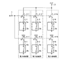
- FIG. 1 is a block diagram showing a variable gain amplifier according to Embodiment 1 of the present invention
- FIG. 2 is a block diagram showing a power amplifier mounted on the variable gain amplifier of FIG. 1 and 2
- a signal input terminal 1 is a terminal for inputting a signal to be amplified.
- the signal input from the signal input terminal 1 is the base with the collector terminal C (second terminal) connected to the signal output terminal 3 and the emitter terminal E (third terminal) connected to the ground.
- the signal amplification transistor 2-n is a grounded-emitter transistor.
- the signal amplification transistor 2-n only needs to be able to amplify a signal.
- the common transistor 2-n may be a transistor with a common collector.
- the signal amplifying transistor 2-n only needs to be able to amplify a signal.
- the type of the signal amplifying transistor 2-n may be, for example, a bipolar transistor or a field effect transistor. .
- the capacitance compensating transistor 4-n is a grounded-emitter transistor, but is not limited to a grounded-emitter transistor, and may be a grounded-collector transistor.
- the capacitance compensation transistor 4-n only needs to have the same input capacitance as the signal amplification transistor 2-n, and the type of the capacitance compensation transistor 4-n may be, for example, a bipolar transistor. However, it may be a field effect transistor.
- the amplification operation of the transistor 2-n is set to an effective state, and the capacitance compensation transistor 4-n is disconnected from the signal input terminal 1 and the ground, while the signal amplification transistor 2-n Is set to an invalid state, and the capacitance compensation transistor 4-n is connected to the signal input terminal 1 and the ground.
- the performance and characteristics of the switch 5-n and the switch 6-n are exactly the same.
- the gain of the variable gain amplifier is determined by the number of signal amplification transistors 2-n in which the amplification operation is valid.
- the switch 5-n connected to the emitter terminal E of the signal amplifying transistor 2-n is turned on by a control circuit (not shown).
- the switch 6-n connected to the emitter terminal E of the capacitance compensating transistor 4-n is set to an off state.
- the switch 5-n connected to the emitter terminal E of the signal amplifying transistor 2-n is turned off by a control circuit (not shown).
- the switch 6-n connected to the emitter terminal E of the capacitance compensating transistor 4-n is set to the on state. Since the switch 5-n is set to the OFF state, the emitter terminal E of the signal amplification transistor 2-n is not connected to the ground, so that the amplification operation of the signal amplification transistor 2-n is invalidated. Become.
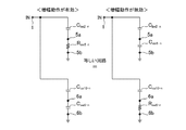
- FIG. 3 is an explanatory diagram showing an equivalent circuit when the amplification operation of the signal amplification transistor 2-n is effective.
- the signal input from the signal input terminal 1 is amplified by the signal amplification transistor 2-n, and the amplified signal is output from the signal output terminal 3. .
- the switch 5-n since the switch 5-n is in the on state, the on-resistance RSW5-n of the switch 5-n exists between the terminals 5a and 5b of the switch 5-n, and the switch 6-n is in the off state. Therefore, the off-capacitance CSW6-n of the switch 6-n exists between the terminal 6a and the terminal 6b of the switch 6-n.
- C be2-n is the input capacitance of the signal amplifying transistor 2-n
- C be4-n is the input capacitance of the capacitance compensating transistor 4-n
- C be2-n C be4-n .
- FIG. 4 is an explanatory diagram showing an equivalent circuit when the amplification operation of the signal amplification transistor 2-n is invalid.
- the signal inputted from the signal input terminal 1 is not amplified by the signal amplification transistor 2-n, and the amplified signal is not outputted from the signal output terminal 3. .
- the switch 5-n since the switch 5-n is in the off state, the off-capacitance CSW5-n of the switch 5-n exists between the terminals 5a and 5b of the switch 5-n, and the switch 6-n is in the on state. Therefore, the on-resistance RSW6-n of the switch 6-n exists between the terminals 6a and 6b of the switch 6-n. Therefore, an equivalent circuit showing the input impedance when the power amplifier is viewed from the signal input terminal 1 is expressed as shown in FIG.
- FIG. 5 is an explanatory diagram showing an equivalent circuit when the amplification operation of the signal amplifying transistor 2-n is valid and an equivalent circuit when the amplification operation is invalid.
- the input capacitance C be4-n of the input capacitance C be2-n and the capacitor compensation transistor 4-n of the signal amplifying transistor 2-n equal.
- the on-resistance R SW5-n of the switch 5-n is equal to the on-resistance R SW6-n of the switch 6-n.
- the off-capacitance C SW5 -n of 5-n is equal to the off-capacitance C SW6-n of the switch 6-n.
- FIG. 6 is an explanatory diagram showing the relationship between the number of signal amplification transistors 2-n and the input impedance when the amplification operation is effective.
- FIG. 7 is an explanatory diagram showing the relationship between the number of signal amplification transistors 2-n and the gain of the variable gain amplifier in a state where the amplification operation is effective.
- the amplification operation of the first transistor is set to an effective state, and the capacitive member is separated from the signal input terminal 1 and the ground.
- a state switching unit for setting the capacitance member to be connected between the signal input terminal 1 and the ground is provided. As a result, it is possible to suppress the fluctuation of the input impedance when the amplification operation is switched from the valid state to the invalid state.
- the first embodiment since a plurality of power amplifiers that can suppress fluctuations in input impedance when the amplification operation is switched from the valid state to the invalid state are connected in parallel. There is an effect that it is possible to suppress a variation in the gain step when the number of first transistors used for power amplification is switched.
- transistors may be used as the first and second switching elements.
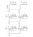
- FIG. 8 is a block diagram showing another power amplifier mounted on the variable gain amplifier of FIG. 1.
- a second switching element that switches a connection state between the ground and the ground.
- the performance and characteristics of the transistor 7-n and the transistor 8-n are exactly the same. Even if the transistor 7-n is used in place of the switch 5-n and the transistor 8-n is used in place of the switch 6-n, as in the case where the switch 5-n and the switch 6-n are used.
- the equivalent circuit when the amplification operation of the signal amplifying transistor 2-n is valid is equivalent to the equivalent circuit when the amplification operation is invalid.
- Embodiment 2 FIG. In the first embodiment, the case where the capacitance compensating transistor 4-n is used as the capacitive member is shown. However, in the second embodiment, the case where the capacitor 10-n is used as the capacitive member is described. To do.
- FIG. 9 is a block diagram showing a variable gain amplifier according to Embodiment 2 of the present invention
- FIG. 10 is a block diagram showing a power amplifier mounted on the variable gain amplifier of FIG. 9 and 10, the same reference numerals as those in FIGS. 1 and 2 indicate the same or corresponding parts, and thus description thereof is omitted.
- the capacitor 10-n has one end connected to the signal input terminal 1 and the other end connected to the terminal 6a of the switch 6-n.
- FIG. 11 is an explanatory diagram showing an equivalent circuit when the amplification operation of the signal amplification transistor 2-n is valid and an equivalent circuit when the amplification operation is invalid.
- the input capacitance C CA10-n of the input capacitance C be2-n and the capacitor 10-n of the signal amplifying transistor 2-n equal.
- the switch 5-n of the on-resistance R SW5-n and the switch 6-n is equal to the on-resistance R SW6-n
- the switch The off-capacitance C SW5 -n of 5-n is equal to the off-capacitance C SW6-n of the switch 6-n.
- the second embodiment also has the effect of suppressing fluctuations in input impedance when the amplification operation is switched between the valid state and the invalid state, as in the first embodiment.
- the transistor 7-n is used instead of the switch 5-n
- the transistor 8-n is used instead of the switch 6-n. May be.
- Embodiment 3 FIG.
- the switch 5-n is connected between the emitter terminal E of the signal amplification transistor 2-n and the ground
- the switch 6-n is connected between the emitter terminal E of the capacitance compensation transistor 4-n and the ground.
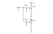
- the switch 11-n is connected between the signal input terminal 1 and the base terminal B of the signal amplification transistor 2-n
- the switch 12-n is input to the signal. What is connected between the terminal 1 and the base terminal B of the capacitance compensating transistor 4-n will be described.
- FIG. 12 is a block diagram showing a variable gain amplifier according to Embodiment 3 of the present invention
- FIG. 13 is a block diagram showing a power amplifier mounted on the variable gain amplifier of FIG. 12 and FIG. 13, the same reference numerals as those in FIG. 1 and FIG.
- the amplification operation of the transistor 2-n is set to an effective state, and the capacitance compensation transistor 4-n is disconnected from the signal input terminal 1 and the ground, while the signal amplification transistor 2-n Is set to an invalid state, and the capacitance compensation transistor 4-n is connected to the signal input terminal 1 and the ground.
- the gain of the variable gain amplifier is determined by the number of signal amplification transistors 2-n in which the amplification operation is valid.
- the switch 11-n connected to the base terminal B of the signal amplifying transistor 2-n is turned on by a control circuit (not shown).
- the switch 12-n connected to the base terminal B of the capacitance compensating transistor 4-n is set to the OFF state. Since the base terminal B of the signal amplification transistor 2-n is connected to the signal input terminal 1 by setting the switch 11-n to the on state, the amplification operation of the signal amplification transistor 2-n Becomes effective.
- a switch 11-n connected to the base terminal B of the signal amplifying transistor 2-n is turned off by a control circuit (not shown).
- the switch 12-n connected to the base terminal B of the capacitance compensating transistor 4-n is set to the ON state. Since the base terminal B of the signal amplification transistor 2-n is not connected to the signal input terminal 1 by setting the switch 11-n to the off state, the amplification operation of the signal amplification transistor 2-n Becomes invalid.
- FIG. 14 is an explanatory diagram showing an equivalent circuit when the amplification operation of the signal amplification transistor 2-n is valid and an equivalent circuit when the amplification operation is invalid.
- the signal input from the signal input terminal 1 is amplified by the signal amplification transistor 2-n, and the amplified signal is output from the signal output terminal 3. .
- the switch 11-n since the switch 11-n is in the on state, the on-resistance RSW11-n of the switch 11-n exists between the terminal 11a and the terminal 11b of the switch 11-n, and the switch 12-n is in the off state.
- FIG. 15 is a block diagram showing another power amplifier implemented in the variable gain amplifier of FIG. 12.
- This is a second switching element that switches between a connection state and a non-connection state between the base terminals B of the transistors for transistor 4-n.
- the performance and characteristics of the transistor 13-n and the transistor 14-n are exactly the same. Even if the transistor 13-n is used in place of the switch 11-n and the transistor 14-n is used in place of the switch 12-n, as in the case where the switch 11-n and the switch 12-n are used.
- the equivalent circuit when the amplification operation of the signal amplifying transistor 2-n is valid is equivalent to the equivalent circuit when the amplification operation is invalid.
- Embodiment 4 FIG.
- the capacitor compensation transistor 4-n is used as the capacitor member.
- the capacitor 15-n is used as the capacitor member. To do.
- FIG. 16 is a block diagram showing a variable gain amplifier according to Embodiment 4 of the present invention
- FIG. 17 is a block diagram showing a power amplifier mounted on the variable gain amplifier of FIG. 16 and FIG. 17, the same reference numerals as those in FIG. 12 and FIG.
- the capacitor 15-n has one end connected to the terminal 12b of the switch 12-n and the other end connected to the ground.
- FIG. 18 is an explanatory diagram showing an equivalent circuit when the amplification operation of the signal amplification transistor 2-n is valid and an equivalent circuit when the amplification operation is invalid.
- the input capacitance C CA15-n of the input capacitance C be2-n and the capacitor 15-n of the signal amplifying transistor 2-n equal.
- the switch 11-n of the on-resistance R SW11-n and the switch 12-n of the on-resistance R SW12-n are equal, the switch 11-n oFF capacitance C SW11-n and the switch 12-n oFF capacitance C SW12-n are equal in.
- the fourth embodiment also has the effect of suppressing fluctuations in input impedance when the amplification operation is switched between the valid state and the invalid state, as in the third embodiment.
- the transistor 13-n is used instead of the switch 11-n, and the transistor 14-n is used instead of the switch 12-n. May be.
- the present invention is suitable for a power amplifier mounted on a variable gain amplifier, and also suitable for a variable gain amplifier whose gain changes.
Abstract
第1のトランジスタの増幅動作を有効な状態に設定して、信号入力端子(1)とグランドの間から容量部材が切り離されている状態に設定する一方、第1のトランジスタの増幅動作を無効な状態に設定して、容量部材が信号入力端子(1)とグランドの間に接続されている状態に設定する状態切換部を備えるように構成する。これにより、増幅動作が有効な状態と無効な状態を切り換えたときの入力インピーダンスの変動を抑えることができる。
Description
この発明は、可変利得増幅器に実装される電力増幅器と、利得が変化する可変利得増幅器とに関するものである。
例えば、無線通信装置やレーダ装置は信号を送信する場合、通信相手との間の距離に応じて、送信信号の電力を調整する必要があり、送信信号の電力を調整する装置として、可変利得増幅器を実装している。
以下の特許文献1に記載されている可変利得増幅器では、利得を可変できるようにするために、N個の信号増幅用トランジスタが並列に接続されている。Nは2以上の整数である。
以下の特許文献1に記載されている可変利得増幅器では、利得を可変できるようにするために、N個の信号増幅用トランジスタが並列に接続されている。Nは2以上の整数である。
この可変利得増幅器は、N個の信号増幅用トランジスタのうち、電力増幅に用いる信号増幅用トランジスタの個数を切り換えることで、利得を調整することができる。
また、この可変利得増幅器は、信号増幅用トランジスタと同数の容量補償用トランジスタを実装しており、容量補償用トランジスタは、信号増幅用トランジスタと同じ入力容量を有している。
容量補償用トランジスタは、対応している信号増幅用トランジスタが電力増幅に用いられているときは動作を停止しており、対応している信号増幅用トランジスタが電力増幅に用いられていないときに動作する。
また、この可変利得増幅器は、信号増幅用トランジスタと同数の容量補償用トランジスタを実装しており、容量補償用トランジスタは、信号増幅用トランジスタと同じ入力容量を有している。
容量補償用トランジスタは、対応している信号増幅用トランジスタが電力増幅に用いられているときは動作を停止しており、対応している信号増幅用トランジスタが電力増幅に用いられていないときに動作する。
従来の可変利得増幅器は以上のように構成されているので、電力増幅に用いる信号増幅用トランジスタの個数を切り換えることで生じる入力インピーダンスの変動を小さくすることはできるが、入力インピーダンスの変動を無くすことはできない。このため、電力増幅に用いる信号増幅用トランジスタの個数を切り換えたときの利得のステップに変動が生じてしまうという課題があった。
この発明は上記のような課題を解決するためになされたもので、増幅動作が有効な状態と無効な状態を切り換えたときの入力インピーダンスの変動を抑えることができる電力増幅器を得ることを目的とする。
また、この発明は、電力増幅に用いる信号増幅用トランジスタの個数を切り換えたときの利得のステップの変動を抑えることができる可変利得増幅器を得ることを目的とする。
また、この発明は、電力増幅に用いる信号増幅用トランジスタの個数を切り換えたときの利得のステップの変動を抑えることができる可変利得増幅器を得ることを目的とする。
この発明に係る電力増幅器は、第1の端子が信号入力端子と接続され、第2の端子が信号出力端子と接続され、第3の端子がグランドと接続されている状態で、信号入力端子から入力された信号が第1の端子に与えられると、その信号を増幅して、第2の端子から増幅後の信号を信号出力端子に出力する第1のトランジスタと、第1のトランジスタの入力容量と同じ入力容量を有する容量部材と、第1のトランジスタの増幅動作を有効な状態に設定して、信号入力端子とグランドの間から容量部材が切り離されている状態に設定する一方、第1のトランジスタの増幅動作を無効な状態に設定して、容量部材が信号入力端子とグランドの間に接続されている状態に設定する状態切換部とを備えるようにしたものである。
この発明によれば、第1のトランジスタの増幅動作を有効な状態に設定して、信号入力端子とグランドの間から容量部材が切り離されている状態に設定する一方、第1のトランジスタの増幅動作を無効な状態に設定して、容量部材が信号入力端子とグランドの間に接続されている状態に設定する状態切換部を備えるように構成したので、増幅動作が有効な状態と無効な状態を切り換えたときの入力インピーダンスの変動を抑えることができる効果がある。
以下、この発明をより詳細に説明するために、この発明を実施するための形態について、添付の図面にしたがって説明する。
実施の形態1.
図1はこの発明の実施の形態1による可変利得増幅器を示す構成図であり、図2は図1の可変利得増幅器に実装される電力増幅器を示す構成図である。
図1及び図2において、信号入力端子1は増幅対象の信号を入力する端子である。
第1のトランジスタである信号増幅用トランジスタ2-n(n=1,2,・・・,N)はエミッタ接地のトランジスタであり、ベース端子B(第1の端子)が信号入力端子1と接続され、コレクタ端子C(第2の端子)が信号出力端子3と接続され、エミッタ端子E(第3の端子)がグランドと接続されている状態で、信号入力端子1から入力された信号がベース端子Bに与えられると、その信号を増幅して、コレクタ端子Cから増幅後の信号を信号出力端子3に出力する。
図1では、信号増幅用トランジスタ2-nの段数がNである例を示しているが、段数Nは、可変利得増幅器における利得の調整分解能によって決まり、例えば、2bitの分解能が求められる場合、N=22-1=3になる。
この実施の形態1では、信号増幅用トランジスタ2-nがエミッタ接地のトランジスタであるものを想定しているが、信号増幅用トランジスタ2-nは信号を増幅することができればよく、例えば、信号増幅用トランジスタ2-nがコレクタ接地のトランジスタであってもよい。
また、信号増幅用トランジスタ2-nは、信号を増幅することができればよく、信号増幅用トランジスタ2-nの種類は、例えば、バイポーラトランジスタであってもよいし、電界効果トランジスタであってもよい。
また、信号増幅用トランジスタ2-nは、信号を増幅することができればよく、信号増幅用トランジスタ2-nの種類は、例えば、バイポーラトランジスタであってもよいし、電界効果トランジスタであってもよい。
信号出力端子3は並列に接続されている信号増幅用トランジスタ2-n(n=1,2,・・・,N)のコレクタ端子Cから出力された増幅後の信号を外部に出力する端子である。
第2のトランジスタである容量補償用トランジスタ4-n(n=1,2,・・・,N)は信号増幅用トランジスタ2-n(n=1,2,・・・,N)と寸法が等しく、信号増幅用トランジスタ2-nと同じ入力容量を有している容量部材である。
容量補償用トランジスタ4-nはベース端子Bが信号入力端子1と接続され、コレクタ端子Cが直流電源VCCと接続され、エミッタ端子Eがスイッチ6-n(n=1,2,・・・,N)の端子6aと接続されている。
この実施の形態1では、容量補償用トランジスタ4-nがエミッタ接地のトランジスタであるものを想定しているが、エミッタ接地のトランジスタに限るものではなく、コレクタ接地のトランジスタであってもよい。
また、容量補償用トランジスタ4-nは、信号増幅用トランジスタ2-nと同じ入力容量を有していればよく、容量補償用トランジスタ4-nの種類は、例えば、バイポーラトランジスタであってもよいし、電界効果トランジスタであってもよい。
スイッチ5-n(n=1,2,・・・,N)及びスイッチ6-n(n=1,2,・・・,N)は状態切換部であり、状態切換部は、信号増幅用トランジスタ2-nの増幅動作を有効な状態に設定して、信号入力端子1とグランドの間から容量補償用トランジスタ4-nが切り離されている状態に設定する一方、信号増幅用トランジスタ2-nの増幅動作を無効な状態に設定して、容量補償用トランジスタ4-nが信号入力端子1とグランドの間に接続されている状態に設定する。
スイッチ5-n(n=1,2,・・・,N)は端子5aが信号増幅用トランジスタ2-nのエミッタ端子Eと接続され、端子5bがグランドと接続されており、信号増幅用トランジスタ2-nのエミッタ端子Eとグランド間の接続と非接続の状態を切り換える第1のスイッチング素子である。
スイッチ6-n(n=1,2,・・・,N)は端子6aが容量補償用トランジスタ4-nのエミッタ端子Eと接続され、端子6bがグランドと接続されており、容量補償用トランジスタ4-nのエミッタ端子Eとグランド間の接続と非接続の状態を切り換える第2のスイッチング素子である。
この実施の形態1では、スイッチ5-nとスイッチ6-nの性能及び特性が全く同じであるものとする。
スイッチ6-n(n=1,2,・・・,N)は端子6aが容量補償用トランジスタ4-nのエミッタ端子Eと接続され、端子6bがグランドと接続されており、容量補償用トランジスタ4-nのエミッタ端子Eとグランド間の接続と非接続の状態を切り換える第2のスイッチング素子である。
この実施の形態1では、スイッチ5-nとスイッチ6-nの性能及び特性が全く同じであるものとする。
次に動作について説明する。
可変利得増幅器の利得は、増幅動作が有効な状態の信号増幅用トランジスタ2-nの個数で決定される。
信号増幅用トランジスタ2-nを増幅動作が有効な状態に設定する場合、図示せぬ制御回路によって、信号増幅用トランジスタ2-nのエミッタ端子Eと接続されているスイッチ5-nがオン状態に設定され、また、容量補償用トランジスタ4-nのエミッタ端子Eと接続されているスイッチ6-nがオフ状態に設定される。
スイッチ5-nがオン状態に設定されることで、信号増幅用トランジスタ2-nのエミッタ端子Eがグランドと接続されている状態になるため、信号増幅用トランジスタ2-nの増幅動作が有効になる。
可変利得増幅器の利得は、増幅動作が有効な状態の信号増幅用トランジスタ2-nの個数で決定される。
信号増幅用トランジスタ2-nを増幅動作が有効な状態に設定する場合、図示せぬ制御回路によって、信号増幅用トランジスタ2-nのエミッタ端子Eと接続されているスイッチ5-nがオン状態に設定され、また、容量補償用トランジスタ4-nのエミッタ端子Eと接続されているスイッチ6-nがオフ状態に設定される。
スイッチ5-nがオン状態に設定されることで、信号増幅用トランジスタ2-nのエミッタ端子Eがグランドと接続されている状態になるため、信号増幅用トランジスタ2-nの増幅動作が有効になる。
信号増幅用トランジスタ2-nを増幅動作が無効な状態に設定する場合、図示せぬ制御回路によって、信号増幅用トランジスタ2-nのエミッタ端子Eと接続されているスイッチ5-nがオフ状態に設定され、また、容量補償用トランジスタ4-nのエミッタ端子Eと接続されているスイッチ6-nがオン状態に設定される。
スイッチ5-nがオフ状態に設定されることで、信号増幅用トランジスタ2-nのエミッタ端子Eがグランドと接続されていない状態になるため、信号増幅用トランジスタ2-nの増幅動作が無効になる。
スイッチ5-nがオフ状態に設定されることで、信号増幅用トランジスタ2-nのエミッタ端子Eがグランドと接続されていない状態になるため、信号増幅用トランジスタ2-nの増幅動作が無効になる。
ここで、図3は信号増幅用トランジスタ2-nの増幅動作が有効である場合の等価回路を示す説明図である。
信号増幅用トランジスタ2-nの増幅動作が有効である場合、信号入力端子1から入力された信号が信号増幅用トランジスタ2-nによって増幅され、信号出力端子3から増幅後の信号が出力される。
このとき、スイッチ5-nはオン状態であるため、スイッチ5-nの端子5aと端子5b間には、スイッチ5-nのオン抵抗RSW5-nが存在し、スイッチ6-nはオフ状態であるため、スイッチ6-nの端子6aと端子6b間には、スイッチ6-nのオフ容量CSW6-nが存在する。
このため、信号入力端子1から電力増幅器を見た入力インピーダンスを示す等価回路は、図3のように表される。図3において、Cbe2-nは信号増幅用トランジスタ2-nの入力容量、Cbe4-nは容量補償用トランジスタ4-nの入力容量であり、Cbe2-n=Cbe4-nである。
図4は信号増幅用トランジスタ2-nの増幅動作が無効である場合の等価回路を示す説明図である。
信号増幅用トランジスタ2-nの増幅動作が無効である場合、信号入力端子1から入力された信号は信号増幅用トランジスタ2-nで増幅されず、信号出力端子3から増幅後の信号が出力されない。
このとき、スイッチ5-nはオフ状態であるため、スイッチ5-nの端子5aと端子5b間には、スイッチ5-nのオフ容量CSW5-nが存在し、スイッチ6-nはオン状態であるため、スイッチ6-nの端子6aと端子6b間には、スイッチ6-nのオン抵抗RSW6-nが存在する。
このため、信号入力端子1から電力増幅器を見た入力インピーダンスを示す等価回路は、図4のように表される。
信号増幅用トランジスタ2-nの増幅動作が無効である場合、信号入力端子1から入力された信号は信号増幅用トランジスタ2-nで増幅されず、信号出力端子3から増幅後の信号が出力されない。
このとき、スイッチ5-nはオフ状態であるため、スイッチ5-nの端子5aと端子5b間には、スイッチ5-nのオフ容量CSW5-nが存在し、スイッチ6-nはオン状態であるため、スイッチ6-nの端子6aと端子6b間には、スイッチ6-nのオン抵抗RSW6-nが存在する。
このため、信号入力端子1から電力増幅器を見た入力インピーダンスを示す等価回路は、図4のように表される。
図5は信号増幅用トランジスタ2-nの増幅動作が有効である場合の等価回路と増幅動作が無効である場合の等価回路とを示す説明図である。
この実施の形態1では、信号増幅用トランジスタ2-nの入力容量Cbe2-nと容量補償用トランジスタ4-nの入力容量Cbe4-nとが等しい。また、スイッチ5-nとスイッチ6-nの性能及び特性が全く同じであるため、スイッチ5-nのオン抵抗RSW5-nとスイッチ6-nのオン抵抗RSW6-nとが等しく、スイッチ5-nのオフ容量CSW5-nとスイッチ6-nのオフ容量CSW6-nとが等しい。
このため、信号増幅用トランジスタ2-nの増幅動作が有効である場合の等価回路と、増幅動作が無効である場合の等価回路とは等しい回路になる。
Cbe2-n=Cbe4-n
RSW5-n=RSW6-n
CSW5-n=CSW6-n
したがって、増幅動作が有効な状態の信号増幅用トランジスタ2-nの個数を変更しても、図6に示すように、信号入力端子1から可変利得増幅器を見た入力インピーダンスは変動しない。このため、増幅動作が有効な状態の信号増幅用トランジスタ2-nの個数を変更しても、図7に示すように、利得のステップの変動を抑えることができる。即ち、利得のステップを一定にすることができる。
図6は増幅動作が有効な状態の信号増幅用トランジスタ2-nの個数と入力インピーダンスとの関係を示す説明図である。
図7は増幅動作が有効な状態の信号増幅用トランジスタ2-nの個数と可変利得増幅器の利得との関係を示す説明図である。
図6は増幅動作が有効な状態の信号増幅用トランジスタ2-nの個数と入力インピーダンスとの関係を示す説明図である。
図7は増幅動作が有効な状態の信号増幅用トランジスタ2-nの個数と可変利得増幅器の利得との関係を示す説明図である。
以上で明らかなように、この実施の形態1によれば、第1のトランジスタの増幅動作を有効な状態に設定して、信号入力端子1とグランドの間から容量部材が切り離されている状態に設定する一方、第1のトランジスタの増幅動作を無効な状態に設定して、容量部材が信号入力端子1とグランドの間に接続されている状態に設定する状態切換部を備えるように構成したので、増幅動作が有効な状態と無効な状態を切り換えたときの入力インピーダンスの変動を抑えることができる効果を奏する。
また、この実施の形態1によれば、増幅動作が有効な状態と無効な状態を切り換えたときの入力インピーダンスの変動を抑えることができる電力増幅器が複数並列に接続されているように構成したので、電力増幅に用いる第1のトランジスタの個数を切り換えたときの利得のステップの変動を抑えることができる効果を奏する。
この実施の形態1では、第1のスイッチング素子としてスイッチ5-n(n=1,2,・・・,N)が用いられ、第2のスイッチング素子としてスイッチ6-n(n=1,2,・・・,N)が用いられているものを示したが、第1及び第2のスイッチング素子としてトランジスタが用いられていてもよい。
図8は図1の可変利得増幅器に実装される他の電力増幅器を示す構成図であり、図8において、図1と同一符号は同一または相当部分を示すので説明を省略する。
トランジスタ7-n(n=1,2,・・・,N)は信号増幅用トランジスタ2-nのエミッタ端子Eとグランドの間に接続されており、信号増幅用トランジスタ2-nのエミッタ端子Eとグランド間の接続と非接続の状態を切り換える第1のスイッチング素子である。
トランジスタ8-n(n=1,2,・・・,N)は容量補償用トランジスタ4-nのエミッタ端子Eとグランドの間に接続されており、容量補償用トランジスタ4-nのエミッタ端子Eとグランド間の接続と非接続の状態を切り換える第2のスイッチング素子である。トランジスタ7-nとトランジスタ8-nの性能及び特性は、全く同じであるものとする。
スイッチ5-nの代わりにトランジスタ7-nが用いられ、スイッチ6-nの代わりにトランジスタ8-nが用いられても、スイッチ5-n及びスイッチ6-nが用いられている場合と同様に、信号増幅用トランジスタ2-nの増幅動作が有効である場合の等価回路と、増幅動作が無効である場合の等価回路とは等しい回路になる。
実施の形態2.
上記実施の形態1では、容量部材として容量補償用トランジスタ4-nが用いられているものを示したが、この実施の形態2では、容量部材としてキャパシタ10-nが用いられているものを説明する。
上記実施の形態1では、容量部材として容量補償用トランジスタ4-nが用いられているものを示したが、この実施の形態2では、容量部材としてキャパシタ10-nが用いられているものを説明する。
図9はこの発明の実施の形態2による可変利得増幅器を示す構成図であり、図10は図9の可変利得増幅器に実装される電力増幅器を示す構成図である。
図9及び図10において、図1及び図2と同一符号は同一または相当部分を示すので説明を省略する。
キャパシタ10-n(n=1,2,・・・,N)は信号増幅用トランジスタ2-nと同じ入力容量を有している容量部材である。
キャパシタ10-nは一端が信号入力端子1と接続され、他端がスイッチ6-nの端子6aと接続されている。
図9及び図10において、図1及び図2と同一符号は同一または相当部分を示すので説明を省略する。
キャパシタ10-n(n=1,2,・・・,N)は信号増幅用トランジスタ2-nと同じ入力容量を有している容量部材である。
キャパシタ10-nは一端が信号入力端子1と接続され、他端がスイッチ6-nの端子6aと接続されている。
図11は信号増幅用トランジスタ2-nの増幅動作が有効である場合の等価回路と増幅動作が無効である場合の等価回路とを示す説明図である。
この実施の形態2では、信号増幅用トランジスタ2-nの入力容量Cbe2-nとキャパシタ10-nの入力容量Cca10-nとが等しい。また、スイッチ5-nとスイッチ6-nの性能及び特性が全く同じであるため、スイッチ5-nのオン抵抗RSW5-nとスイッチ6-nのオン抵抗RSW6-nとが等しく、スイッチ5-nのオフ容量CSW5-nとスイッチ6-nのオフ容量CSW6-nとが等しい。
このため、信号増幅用トランジスタ2-nの増幅動作が有効である場合の等価回路と、増幅動作が無効である場合の等価回路とは等しい回路になる。
Cbe2-n=Cca10-n
RSW5-n=RSW6-n
CSW5-n=CSW6-n
この実施の形態2では、信号増幅用トランジスタ2-nの入力容量Cbe2-nとキャパシタ10-nの入力容量Cca10-nとが等しい。また、スイッチ5-nとスイッチ6-nの性能及び特性が全く同じであるため、スイッチ5-nのオン抵抗RSW5-nとスイッチ6-nのオン抵抗RSW6-nとが等しく、スイッチ5-nのオフ容量CSW5-nとスイッチ6-nのオフ容量CSW6-nとが等しい。
このため、信号増幅用トランジスタ2-nの増幅動作が有効である場合の等価回路と、増幅動作が無効である場合の等価回路とは等しい回路になる。
Cbe2-n=Cca10-n
RSW5-n=RSW6-n
CSW5-n=CSW6-n
したがって、増幅動作が有効な状態の信号増幅用トランジスタ2-nの個数を変更しても、図6に示すように、信号入力端子1から可変利得増幅器を見た入力インピーダンスは変動しない。このため、増幅動作が有効な状態の信号増幅用トランジスタ2-nの個数を変更しても、図7に示すように、利得のステップの変動を抑えることができる。即ち、利得のステップを一定にすることができる。
これにより、この実施の形態2でも、上記実施の形態1と同様に、増幅動作が有効な状態と無効な状態を切り換えたときの入力インピーダンスの変動を抑えることができる効果を奏する。
また、電力増幅に用いる信号増幅用トランジスタ2-nの個数を切り換えたときの利得のステップの変動を抑えることができる効果を奏する。
なお、容量補償用トランジスタ4-nの代わりに、キャパシタ10-nを用いたことにより、上記実施の形態1よりも省電力化を図ることができる。
これにより、この実施の形態2でも、上記実施の形態1と同様に、増幅動作が有効な状態と無効な状態を切り換えたときの入力インピーダンスの変動を抑えることができる効果を奏する。
また、電力増幅に用いる信号増幅用トランジスタ2-nの個数を切り換えたときの利得のステップの変動を抑えることができる効果を奏する。
なお、容量補償用トランジスタ4-nの代わりに、キャパシタ10-nを用いたことにより、上記実施の形態1よりも省電力化を図ることができる。
この実施の形態2でも、上記実施の形態1と同様に、スイッチ5-nの代わりにトランジスタ7-nが用いられ、スイッチ6-nの代わりにトランジスタ8-nが用いられているものであってもよい。
実施の形態3.
上記実施の形態1では、スイッチ5-nが信号増幅用トランジスタ2-nのエミッタ端子Eとグランド間に接続され、スイッチ6-nが容量補償用トランジスタ4-nのエミッタ端子Eとグランド間に接続されているものを示したが、この実施の形態3では、スイッチ11-nが信号入力端子1と信号増幅用トランジスタ2-nのベース端子B間に接続され、スイッチ12-nが信号入力端子1と容量補償用トランジスタ4-nのベース端子B間に接続されているものについて説明する。
上記実施の形態1では、スイッチ5-nが信号増幅用トランジスタ2-nのエミッタ端子Eとグランド間に接続され、スイッチ6-nが容量補償用トランジスタ4-nのエミッタ端子Eとグランド間に接続されているものを示したが、この実施の形態3では、スイッチ11-nが信号入力端子1と信号増幅用トランジスタ2-nのベース端子B間に接続され、スイッチ12-nが信号入力端子1と容量補償用トランジスタ4-nのベース端子B間に接続されているものについて説明する。
図12はこの発明の実施の形態3による可変利得増幅器を示す構成図であり、図13は図12の可変利得増幅器に実装される電力増幅器を示す構成図である。
図12及び図13において、図1及び図2と同一符号は同一または相当部分を示すので説明を省略する。
スイッチ11-n(n=1,2,・・・,N)及びスイッチ12-n(n=1,2,・・・,N)は状態切換部であり、状態切換部は、信号増幅用トランジスタ2-nの増幅動作を有効な状態に設定して、信号入力端子1とグランドの間から容量補償用トランジスタ4-nが切り離されている状態に設定する一方、信号増幅用トランジスタ2-nの増幅動作を無効な状態に設定して、容量補償用トランジスタ4-nが信号入力端子1とグランドの間に接続されている状態に設定する。
図12及び図13において、図1及び図2と同一符号は同一または相当部分を示すので説明を省略する。
スイッチ11-n(n=1,2,・・・,N)及びスイッチ12-n(n=1,2,・・・,N)は状態切換部であり、状態切換部は、信号増幅用トランジスタ2-nの増幅動作を有効な状態に設定して、信号入力端子1とグランドの間から容量補償用トランジスタ4-nが切り離されている状態に設定する一方、信号増幅用トランジスタ2-nの増幅動作を無効な状態に設定して、容量補償用トランジスタ4-nが信号入力端子1とグランドの間に接続されている状態に設定する。
スイッチ11-n(n=1,2,・・・,N)は端子11aが信号入力端子1と接続され、端子11bが信号増幅用トランジスタ2-nのベース端子Bと接続されており、信号入力端子1と信号増幅用トランジスタ2-nのベース端子B間の接続と非接続の状態を切り換える第1のスイッチング素子である。
スイッチ12-n(n=1,2,・・・,N)は端子12aが信号入力端子1と接続され、端子12bが容量補償用トランジスタ4-nのベース端子Bと接続されており、信号入力端子1と容量補償用トランジスタ4-nのベース端子B間の接続と非接続の状態を切り換える第2のスイッチング素子である。
この実施の形態3では、スイッチ11-nとスイッチ12-nの性能及び特性が全く同じであるものとする。
スイッチ12-n(n=1,2,・・・,N)は端子12aが信号入力端子1と接続され、端子12bが容量補償用トランジスタ4-nのベース端子Bと接続されており、信号入力端子1と容量補償用トランジスタ4-nのベース端子B間の接続と非接続の状態を切り換える第2のスイッチング素子である。
この実施の形態3では、スイッチ11-nとスイッチ12-nの性能及び特性が全く同じであるものとする。
次に動作について説明する。
可変利得増幅器の利得は、増幅動作が有効な状態の信号増幅用トランジスタ2-nの個数で決定される。
信号増幅用トランジスタ2-nを増幅動作が有効な状態に設定する場合、図示せぬ制御回路によって、信号増幅用トランジスタ2-nのベース端子Bと接続されているスイッチ11-nがオン状態に設定され、また、容量補償用トランジスタ4-nのベース端子Bと接続されているスイッチ12-nがオフ状態に設定される。
スイッチ11-nがオン状態に設定されることで、信号増幅用トランジスタ2-nのベース端子Bが信号入力端子1と接続されている状態になるため、信号増幅用トランジスタ2-nの増幅動作が有効になる。
可変利得増幅器の利得は、増幅動作が有効な状態の信号増幅用トランジスタ2-nの個数で決定される。
信号増幅用トランジスタ2-nを増幅動作が有効な状態に設定する場合、図示せぬ制御回路によって、信号増幅用トランジスタ2-nのベース端子Bと接続されているスイッチ11-nがオン状態に設定され、また、容量補償用トランジスタ4-nのベース端子Bと接続されているスイッチ12-nがオフ状態に設定される。
スイッチ11-nがオン状態に設定されることで、信号増幅用トランジスタ2-nのベース端子Bが信号入力端子1と接続されている状態になるため、信号増幅用トランジスタ2-nの増幅動作が有効になる。
信号増幅用トランジスタ2-nを増幅動作が無効な状態に設定する場合、図示せぬ制御回路によって、信号増幅用トランジスタ2-nのベース端子Bと接続されているスイッチ11-nがオフ状態に設定され、また、容量補償用トランジスタ4-nのベース端子Bと接続されているスイッチ12-nがオン状態に設定される。
スイッチ11-nがオフ状態に設定されることで、信号増幅用トランジスタ2-nのベース端子Bが信号入力端子1と接続されていない状態になるため、信号増幅用トランジスタ2-nの増幅動作が無効になる。
スイッチ11-nがオフ状態に設定されることで、信号増幅用トランジスタ2-nのベース端子Bが信号入力端子1と接続されていない状態になるため、信号増幅用トランジスタ2-nの増幅動作が無効になる。
図14は信号増幅用トランジスタ2-nの増幅動作が有効である場合の等価回路と増幅動作が無効である場合の等価回路とを示す説明図である。
信号増幅用トランジスタ2-nの増幅動作が有効である場合、信号入力端子1から入力された信号が信号増幅用トランジスタ2-nによって増幅され、信号出力端子3から増幅後の信号が出力される。
このとき、スイッチ11-nはオン状態であるため、スイッチ11-nの端子11aと端子11b間には、スイッチ11-nのオン抵抗RSW11-nが存在し、スイッチ12-nはオフ状態であるため、スイッチ12-nの端子12aと端子12b間には、スイッチ12-nのオフ容量CSW12-nが存在する。
このため、信号入力端子1から電力増幅器を見た入力インピーダンスを示す等価回路は、図14の左図のように表される。
信号増幅用トランジスタ2-nの増幅動作が有効である場合、信号入力端子1から入力された信号が信号増幅用トランジスタ2-nによって増幅され、信号出力端子3から増幅後の信号が出力される。
このとき、スイッチ11-nはオン状態であるため、スイッチ11-nの端子11aと端子11b間には、スイッチ11-nのオン抵抗RSW11-nが存在し、スイッチ12-nはオフ状態であるため、スイッチ12-nの端子12aと端子12b間には、スイッチ12-nのオフ容量CSW12-nが存在する。
このため、信号入力端子1から電力増幅器を見た入力インピーダンスを示す等価回路は、図14の左図のように表される。
信号増幅用トランジスタ2-nの増幅動作が無効である場合、信号入力端子1から入力された信号は信号増幅用トランジスタ2-nで増幅されず、信号出力端子3から増幅後の信号が出力されない。
このとき、スイッチ11-nはオフ状態であるため、スイッチ11-nの端子11aと端子11b間には、スイッチ11-nのオフ容量CSW11-nが存在し、スイッチ12-nはオン状態であるため、スイッチ12-nの端子12aと端子12b間には、スイッチ12-nのオン抵抗RSW12-nが存在する。
このため、信号入力端子1から電力増幅器を見た入力インピーダンスを示す等価回路は、図14の右図のように表される。
このとき、スイッチ11-nはオフ状態であるため、スイッチ11-nの端子11aと端子11b間には、スイッチ11-nのオフ容量CSW11-nが存在し、スイッチ12-nはオン状態であるため、スイッチ12-nの端子12aと端子12b間には、スイッチ12-nのオン抵抗RSW12-nが存在する。
このため、信号入力端子1から電力増幅器を見た入力インピーダンスを示す等価回路は、図14の右図のように表される。
この実施の形態3では、信号増幅用トランジスタ2-nの入力容量Cbe2-nと容量補償用トランジスタ4-nの入力容量Cbe4-nとが等しい。また、スイッチ11-nとスイッチ12-nの性能及び特性が全く同じであるため、スイッチ11-nのオン抵抗RSW11-nとスイッチ12-nのオン抵抗RSW12-nとが等しく、スイッチ11-nのオフ容量CSW11-nとスイッチ12-nのオフ容量CSW12-nとが等しい。
このため、信号増幅用トランジスタ2-nの増幅動作が有効である場合の等価回路と、増幅動作が無効である場合の等価回路とは等しい回路になる。
Cbe2-n=Cbe4-n
RSW11-n=RSW12-n
CSW11-n=CSW12-n
このため、信号増幅用トランジスタ2-nの増幅動作が有効である場合の等価回路と、増幅動作が無効である場合の等価回路とは等しい回路になる。
Cbe2-n=Cbe4-n
RSW11-n=RSW12-n
CSW11-n=CSW12-n
したがって、増幅動作が有効な状態の信号増幅用トランジスタ2-nの個数を変更しても、図6に示すように、信号入力端子1から可変利得増幅器を見た入力インピーダンスは変動しない。このため、増幅動作が有効な状態の信号増幅用トランジスタ2-nの個数を変更しても、図7に示すように、利得のステップの変動を抑えることができる。即ち、利得のステップを一定にすることができる。
これにより、この実施の形態3でも、上記実施の形態1と同様に、増幅動作が有効な状態と無効な状態を切り換えたときの入力インピーダンスの変動を抑えることができる効果を奏する。
また、電力増幅に用いる信号増幅用トランジスタ2-nの個数を切り換えたときの利得のステップの変動を抑えることができる効果を奏する。
これにより、この実施の形態3でも、上記実施の形態1と同様に、増幅動作が有効な状態と無効な状態を切り換えたときの入力インピーダンスの変動を抑えることができる効果を奏する。
また、電力増幅に用いる信号増幅用トランジスタ2-nの個数を切り換えたときの利得のステップの変動を抑えることができる効果を奏する。
この実施の形態3では、第1のスイッチング素子としてスイッチ11-n(n=1,2,・・・,N)が用いられ、第2のスイッチング素子としてスイッチ12-n(n=1,2,・・・,N)が用いられているものを示したが、第1及び第2のスイッチング素子としてトランジスタが用いられていてもよい。
図15は図12の可変利得増幅器に実装される他の電力増幅器を示す構成図であり、図15において、図13と同一符号は同一または相当部分を示すので説明を省略する。
トランジスタ13-n(n=1,2,・・・,N)は信号入力端子1と信号増幅用トランジスタ2-nのベース端子Bとの間に接続されており、信号入力端子1と信号増幅用トランジスタ2-nのベース端子B間の接続と非接続の状態を切り換える第1のスイッチング素子である。
トランジスタ14-n(n=1,2,・・・,N)は信号入力端子1と容量補償用トランジスタ4-nのベース端子Bとの間に接続されており、信号入力端子1と容量補償用トランジスタ4-nのベース端子B間の接続と非接続の状態を切り換える第2のスイッチング素子である。トランジスタ13-nとトランジスタ14-nの性能及び特性は、全く同じであるものとする。
スイッチ11-nの代わりにトランジスタ13-nが用いられ、スイッチ12-nの代わりにトランジスタ14-nが用いられても、スイッチ11-n及びスイッチ12-nが用いられている場合と同様に、信号増幅用トランジスタ2-nの増幅動作が有効である場合の等価回路と、増幅動作が無効である場合の等価回路とは等しい回路になる。
実施の形態4.
上記実施の形態3では、容量部材として容量補償用トランジスタ4-nが用いられているものを示したが、この実施の形態4では、容量部材としてキャパシタ15-nが用いられているものを説明する。
上記実施の形態3では、容量部材として容量補償用トランジスタ4-nが用いられているものを示したが、この実施の形態4では、容量部材としてキャパシタ15-nが用いられているものを説明する。
図16はこの発明の実施の形態4による可変利得増幅器を示す構成図であり、図17は図16の可変利得増幅器に実装される電力増幅器を示す構成図である。
図16及び図17において、図12及び図13と同一符号は同一または相当部分を示すので説明を省略する。
キャパシタ15-n(n=1,2,・・・,N)は信号増幅用トランジスタ2-nと同じ入力容量を有している容量部材である。
キャパシタ15-nは一端がスイッチ12-nの端子12bと接続され、他端がグランドと接続されている。
図16及び図17において、図12及び図13と同一符号は同一または相当部分を示すので説明を省略する。
キャパシタ15-n(n=1,2,・・・,N)は信号増幅用トランジスタ2-nと同じ入力容量を有している容量部材である。
キャパシタ15-nは一端がスイッチ12-nの端子12bと接続され、他端がグランドと接続されている。
図18は信号増幅用トランジスタ2-nの増幅動作が有効である場合の等価回路と増幅動作が無効である場合の等価回路とを示す説明図である。
この実施の形態4では、信号増幅用トランジスタ2-nの入力容量Cbe2-nとキャパシタ15-nの入力容量Cca15-nとが等しい。また、スイッチ11-nとスイッチ12-nの性能及び特性が全く同じであるため、スイッチ11-nのオン抵抗RSW11-nとスイッチ12-nのオン抵抗RSW12-nとが等しく、スイッチ11-nのオフ容量CSW11-nとスイッチ12-nのオフ容量CSW12-nとが等しい。
このため、信号増幅用トランジスタ2-nの増幅動作が有効である場合の等価回路と、増幅動作が無効である場合の等価回路とは等しい回路になる。
Cbe2-n=Cca15-n
RSW11-n=RSW12-n
CSW11-n=CSW12-n
したがって、増幅動作が有効な状態の信号増幅用トランジスタ2-nの個数を変更しても、図6に示すように、信号入力端子1から可変利得増幅器を見た入力インピーダンスは変動しない。このため、増幅動作が有効な状態の信号増幅用トランジスタ2-nの個数を変更しても、図7に示すように、利得のステップの変動を抑えることができる。即ち、利得のステップを一定にすることができる。
これにより、この実施の形態4でも、上記実施の形態3と同様に、増幅動作が有効な状態と無効な状態を切り換えたときの入力インピーダンスの変動を抑えることができる効果を奏する。
また、電力増幅に用いる信号増幅用トランジスタ2-nの個数を切り換えたときの利得のステップの変動を抑えることができる効果を奏する。
なお、容量補償用トランジスタ4-nの代わりに、キャパシタ15-nを用いたことにより、上記実施の形態3よりも省電力化を図ることができる。
これにより、この実施の形態4でも、上記実施の形態3と同様に、増幅動作が有効な状態と無効な状態を切り換えたときの入力インピーダンスの変動を抑えることができる効果を奏する。
また、電力増幅に用いる信号増幅用トランジスタ2-nの個数を切り換えたときの利得のステップの変動を抑えることができる効果を奏する。
なお、容量補償用トランジスタ4-nの代わりに、キャパシタ15-nを用いたことにより、上記実施の形態3よりも省電力化を図ることができる。
この実施の形態4でも、上記実施の形態3と同様に、スイッチ11-nの代わりにトランジスタ13-nが用いられ、スイッチ12-nの代わりにトランジスタ14-nが用いられているものであってもよい。
なお、本願発明はその発明の範囲内において、各実施の形態の自由な組み合わせ、あるいは各実施の形態の任意の構成要素の変形、もしくは各実施の形態において任意の構成要素の省略が可能である。
この発明は、可変利得増幅器に実装されている電力増幅器に適しており、また、利得が変化する可変利得増幅器に適している。
1 信号入力端子、2-1~2-N 信号増幅用トランジスタ(第1のトランジスタ)、3 信号出力端子、4-1~4-N 容量補償用トランジスタ(容量部材、第2のトランジスタ)、5-1~5-N スイッチ(状態切換部、第1のスイッチング素子)、5a,5b 端子、6-1~6-N スイッチ(状態切換部、第2のスイッチング素子)、6a,6b 端子、7-1~7-N トランジスタ(状態切換部、第1のスイッチング素子)、8-1~8-N トランジスタ(状態切換部、第2のスイッチング素子)、10-1~10-N キャパシタ(容量部材)、11-1~11-N スイッチ(状態切換部、第1のスイッチング素子)、11a,11b 端子、12-1~12-N スイッチ(状態切換部、第2のスイッチング素子)、12a,12b 端子、13-1~13-N トランジスタ(状態切換部、第1のスイッチング素子)、14-1~14-N トランジスタ(状態切換部、第2のスイッチング素子)、15-1~15-N キャパシタ(容量部材)。
Claims (9)
- 第1の端子が信号入力端子と接続され、第2の端子が信号出力端子と接続され、第3の端子がグランドと接続されている状態で、前記信号入力端子から入力された信号が前記第1の端子に与えられると、前記信号を増幅して、前記第2の端子から増幅後の信号を前記信号出力端子に出力する第1のトランジスタと、
前記第1のトランジスタの入力容量と同じ入力容量を有する容量部材と、
前記第1のトランジスタの増幅動作を有効な状態に設定して、前記信号入力端子と前記グランドの間から前記容量部材が切り離されている状態に設定する一方、前記第1のトランジスタの増幅動作を無効な状態に設定して、前記容量部材が前記信号入力端子と前記グランドの間に接続されている状態に設定する状態切換部と
を備えた電力増幅器。 - 前記容量部材として、第2のトランジスタが用いられており、
前記状態切換部によって、前記第1のトランジスタの増幅動作が無効な状態に設定された場合、前記第2のトランジスタの第1の端子が前記信号入力端子と接続され、前記第2のトランジスタの第2の端子が電源と接続され、前記第2のトランジスタの第3の端子が前記グランドと接続されることを特徴とする請求項1記載の電力増幅器。 - 前記状態切換部は、
前記第1のトランジスタの第3の端子と前記グランド間の接続と非接続の状態を切り換える第1のスイッチング素子と、
前記第2のトランジスタの第3の端子と前記グランド間の接続と非接続の状態を切り換える第2のスイッチング素子とを備えていることを特徴とする請求項2記載の電力増幅器。 - 前記状態切換部は、
前記トランジスタの第1の端子と前記信号入力端子間の接続と非接続の状態を切り換える第1のスイッチング素子と、
前記第2のトランジスタの第1の端子と前記信号入力端子間の接続と非接続の状態を切り換える第2のスイッチング素子とを備えていることを特徴とする請求項2記載の電力増幅器。 - 前記第2のトランジスタが電界効果トランジスタであることを特徴とする請求項2記載の電力増幅器。
- 前記容量部材として、キャパシタが用いられており、
前記状態切換部によって、前記第1のトランジスタの増幅動作が無効な状態に設定された場合、前記キャパシタの一端が前記信号入力端子と接続され、前記キャパシタの他端が前記グランドと接続されることを特徴とする請求項1記載の電力増幅器。 - 前記状態切換部は、
前記第1のトランジスタの第3の端子と前記グランド間の接続と非接続の状態を切り換える第1のスイッチング素子と、
前記キャパシタと前記グランド間の接続と非接続の状態を切り換える第2のスイッチング素子とを備えていることを特徴とする請求項6記載の電力増幅器。 - 前記状態切換部は、
前記トランジスタの第1の端子と前記信号入力端子間の接続と非接続の状態を切り換える第1のスイッチング素子と、
前記信号入力端子と前記キャパシタ間の接続と非接続の状態を切り換える第2のスイッチング素子とを備えていることを特徴とする請求項6記載の電力増幅器。 - 第1の端子が信号入力端子と接続され、第2の端子が信号出力端子と接続され、第3の端子がグランドと接続されている状態で、前記信号入力端子から入力された信号が前記第1の端子に与えられると、前記信号を増幅して、前記第2の端子から増幅後の信号を前記信号出力端子に出力する第1のトランジスタと、
前記第1のトランジスタの入力容量と同じ入力容量を有する容量部材と、
前記第1のトランジスタの増幅動作を有効な状態に設定して、前記信号入力端子と前記グランドの間から前記容量部材が切り離されている状態に設定する一方、前記第1のトランジスタの増幅動作を無効な状態に設定して、前記容量部材が前記信号入力端子と前記グランドの間に接続されている状態に設定する状態切換部とを備え、
前記第1のトランジスタ、前記容量部材及び前記状態切換部の組が複数並列に接続されていることを特徴とする可変利得増幅器。
Priority Applications (2)
| Application Number | Priority Date | Filing Date | Title |
|---|---|---|---|
| PCT/JP2016/068948 WO2018002978A1 (ja) | 2016-06-27 | 2016-06-27 | 電力増幅器及び可変利得増幅器 |
| JP2016572845A JP6104485B1 (ja) | 2016-06-27 | 2016-06-27 | 電力増幅器及び可変利得増幅器 |
Applications Claiming Priority (1)
| Application Number | Priority Date | Filing Date | Title |
|---|---|---|---|
| PCT/JP2016/068948 WO2018002978A1 (ja) | 2016-06-27 | 2016-06-27 | 電力増幅器及び可変利得増幅器 |
Publications (1)
| Publication Number | Publication Date |
|---|---|
| WO2018002978A1 true WO2018002978A1 (ja) | 2018-01-04 |
Family
ID=59366101
Family Applications (1)
| Application Number | Title | Priority Date | Filing Date |
|---|---|---|---|
| PCT/JP2016/068948 WO2018002978A1 (ja) | 2016-06-27 | 2016-06-27 | 電力増幅器及び可変利得増幅器 |
Country Status (2)
| Country | Link |
|---|---|
| JP (1) | JP6104485B1 (ja) |
| WO (1) | WO2018002978A1 (ja) |
Citations (4)
| Publication number | Priority date | Publication date | Assignee | Title |
|---|---|---|---|---|
| JP2000101371A (ja) * | 1998-09-28 | 2000-04-07 | Matsushita Electric Ind Co Ltd | 可変利得増幅器 |
| JP2010239401A (ja) * | 2009-03-31 | 2010-10-21 | Panasonic Corp | 可変利得増幅回路および無線通信装置 |
| JP2011119987A (ja) * | 2009-12-03 | 2011-06-16 | Renesas Electronics Corp | 半導体集積回路装置 |
| WO2012100947A1 (en) * | 2011-01-27 | 2012-08-02 | St-Ericsson Sa | Amplification circuit having optimization of power |
-
2016
- 2016-06-27 JP JP2016572845A patent/JP6104485B1/ja active Active
- 2016-06-27 WO PCT/JP2016/068948 patent/WO2018002978A1/ja active Application Filing
Patent Citations (4)
| Publication number | Priority date | Publication date | Assignee | Title |
|---|---|---|---|---|
| JP2000101371A (ja) * | 1998-09-28 | 2000-04-07 | Matsushita Electric Ind Co Ltd | 可変利得増幅器 |
| JP2010239401A (ja) * | 2009-03-31 | 2010-10-21 | Panasonic Corp | 可変利得増幅回路および無線通信装置 |
| JP2011119987A (ja) * | 2009-12-03 | 2011-06-16 | Renesas Electronics Corp | 半導体集積回路装置 |
| WO2012100947A1 (en) * | 2011-01-27 | 2012-08-02 | St-Ericsson Sa | Amplification circuit having optimization of power |
Also Published As
| Publication number | Publication date |
|---|---|
| JPWO2018002978A1 (ja) | 2018-06-28 |
| JP6104485B1 (ja) | 2017-03-29 |
Similar Documents
| Publication | Publication Date | Title |
|---|---|---|
| KR101719310B1 (ko) | 듀얼 동작 모드 전력 증폭기 | |
| US8395448B2 (en) | Apparatus and method for miller compensation for multi-stage amplifier | |
| US9118282B2 (en) | Power amplifier and amplification method thereof | |
| CN101904093B (zh) | 高速多级ab类放大器 | |
| US10211797B2 (en) | Bidirectional amplifier | |
| US7538605B2 (en) | Amplifier device capable of reducing offset voltage | |
| JPWO2007105282A1 (ja) | ゲイン可変増幅器 | |
| US7405626B2 (en) | Distributed amplifier having a variable terminal resistance | |
| JP2007221402A (ja) | 可変利得増幅器及びその半導体集積装置 | |
| US9667202B2 (en) | Power amplifier and method | |
| JP3830724B2 (ja) | 増幅器 | |
| WO2018002978A1 (ja) | 電力増幅器及び可変利得増幅器 | |
| US10122337B2 (en) | Programmable gain amplifier | |
| KR100835057B1 (ko) | 분포형 전력 증폭기 | |
| JP2020150523A (ja) | 半導体回路 | |
| WO2014083876A1 (ja) | 電力増幅回路及び電力増幅モジュール | |
| JP5694035B2 (ja) | 電力増幅器および通信装置 | |
| JP5472488B2 (ja) | 増幅装置 | |
| WO2018037688A1 (ja) | 信号増幅装置 | |
| CN219304802U (zh) | 放大器、射频电路及电子设备 | |
| CN213585709U (zh) | 带宽可重构的射频功率放大器 | |
| US11146218B2 (en) | Amplification circuit | |
| US10763793B2 (en) | Dual-mode signal amplifying circuit of signal receiver | |
| JP4370932B2 (ja) | マイクロ波増幅回路 | |
| KR102487060B1 (ko) | 소형 광대역 증폭기 회로 |
Legal Events
| Date | Code | Title | Description |
|---|---|---|---|
| ENP | Entry into the national phase |
Ref document number: 2016572845 Country of ref document: JP Kind code of ref document: A |
|
| 121 | Ep: the epo has been informed by wipo that ep was designated in this application |
Ref document number: 16907212 Country of ref document: EP Kind code of ref document: A1 |
|
| NENP | Non-entry into the national phase |
Ref country code: DE |
|
| 122 | Ep: pct application non-entry in european phase |
Ref document number: 16907212 Country of ref document: EP Kind code of ref document: A1 |