WO2017221478A1 - 電界放射装置および改質処理方法 - Google Patents
電界放射装置および改質処理方法 Download PDFInfo
- Publication number
- WO2017221478A1 WO2017221478A1 PCT/JP2017/010550 JP2017010550W WO2017221478A1 WO 2017221478 A1 WO2017221478 A1 WO 2017221478A1 JP 2017010550 W JP2017010550 W JP 2017010550W WO 2017221478 A1 WO2017221478 A1 WO 2017221478A1
- Authority
- WO
- WIPO (PCT)
- Prior art keywords
- emitter
- vacuum chamber
- guard electrode
- field emission
- movement
- Prior art date
- Legal status (The legal status is an assumption and is not a legal conclusion. Google has not performed a legal analysis and makes no representation as to the accuracy of the status listed.)
- Ceased
Links
Images


Classifications
-
- H—ELECTRICITY
- H01—ELECTRIC ELEMENTS
- H01J—ELECTRIC DISCHARGE TUBES OR DISCHARGE LAMPS
- H01J35/00—X-ray tubes
- H01J35/02—Details
- H01J35/04—Electrodes ; Mutual position thereof; Constructional adaptations therefor
- H01J35/06—Cathodes
- H01J35/065—Field emission, photo emission or secondary emission cathodes
-
- H—ELECTRICITY
- H01—ELECTRIC ELEMENTS
- H01J—ELECTRIC DISCHARGE TUBES OR DISCHARGE LAMPS
- H01J1/00—Details of electrodes, of magnetic control means, of screens, or of the mounting or spacing thereof, common to two or more basic types of discharge tubes or lamps
- H01J1/02—Main electrodes
- H01J1/30—Cold cathodes, e.g. field-emissive cathode
- H01J1/304—Field-emissive cathodes
-
- H—ELECTRICITY
- H01—ELECTRIC ELEMENTS
- H01J—ELECTRIC DISCHARGE TUBES OR DISCHARGE LAMPS
- H01J9/00—Apparatus or processes specially adapted for the manufacture, installation, removal, maintenance of electric discharge tubes, discharge lamps, or parts thereof; Recovery of material from discharge tubes or lamps
- H01J9/50—Repairing or regenerating used or defective discharge tubes or lamps
-
- H—ELECTRICITY
- H05—ELECTRIC TECHNIQUES NOT OTHERWISE PROVIDED FOR
- H05G—X-RAY TECHNIQUE
- H05G1/00—X-ray apparatus involving X-ray tubes; Circuits therefor
-
- H—ELECTRICITY
- H05—ELECTRIC TECHNIQUES NOT OTHERWISE PROVIDED FOR
- H05G—X-RAY TECHNIQUE
- H05G1/00—X-ray apparatus involving X-ray tubes; Circuits therefor
- H05G1/02—Constructional details
-
- H—ELECTRICITY
- H01—ELECTRIC ELEMENTS
- H01J—ELECTRIC DISCHARGE TUBES OR DISCHARGE LAMPS
- H01J2201/00—Electrodes common to discharge tubes
- H01J2201/30—Cold cathodes
- H01J2201/304—Field emission cathodes
- H01J2201/30446—Field emission cathodes characterised by the emitter material
- H01J2201/30453—Carbon types
-
- H—ELECTRICITY
- H01—ELECTRIC ELEMENTS
- H01J—ELECTRIC DISCHARGE TUBES OR DISCHARGE LAMPS
- H01J2235/00—X-ray tubes
- H01J2235/06—Cathode assembly
- H01J2235/062—Cold cathodes
-
- H—ELECTRICITY
- H01—ELECTRIC ELEMENTS
- H01J—ELECTRIC DISCHARGE TUBES OR DISCHARGE LAMPS
- H01J2235/00—X-ray tubes
- H01J2235/06—Cathode assembly
- H01J2235/064—Movement of cathode
-
- Y—GENERAL TAGGING OF NEW TECHNOLOGICAL DEVELOPMENTS; GENERAL TAGGING OF CROSS-SECTIONAL TECHNOLOGIES SPANNING OVER SEVERAL SECTIONS OF THE IPC; TECHNICAL SUBJECTS COVERED BY FORMER USPC CROSS-REFERENCE ART COLLECTIONS [XRACs] AND DIGESTS
- Y02—TECHNOLOGIES OR APPLICATIONS FOR MITIGATION OR ADAPTATION AGAINST CLIMATE CHANGE
- Y02W—CLIMATE CHANGE MITIGATION TECHNOLOGIES RELATED TO WASTEWATER TREATMENT OR WASTE MANAGEMENT
- Y02W30/00—Technologies for solid waste management
- Y02W30/50—Reuse, recycling or recovery technologies
- Y02W30/82—Recycling of waste of electrical or electronic equipment [WEEE]
Definitions
- the present invention relates to a field emission apparatus and a modification treatment method applied to various devices such as an X-ray apparatus, an electron tube, and an illumination apparatus.
- a field emission device applied to various devices such as an X-ray device, an electron tube, and an illumination device
- emitters carbon or the like positioned in opposite directions (a predetermined distance apart) in a vacuum chamber of a vacuum vessel
- a voltage is applied between the electron source used and the target, the electron beam is emitted by field emission (emission and generation of electrons) of the emitter, and the emitted electron beam collides with the target to obtain the desired function
- X-ray apparatus a configuration is known which exerts a fluoroscopic resolution (X) by external emission of X-rays.
- a grid electrode or the like is interposed between the emitter and the target to form a triode structure, or the surface of the electron generating portion of the emitter (the portion located on the side facing the target and generating electrons) is curved It has been studied to suppress the dispersion of the electron beam emitted from the emitter by, for example, disposing a guard electrode at the same potential as the emitter on the outer peripheral side of the emitter (for example, Patent Documents 1 and 2).
- a portion susceptible to local electric field concentration is formed (eg, minute projections formed in processing) If the gas component (for example, the gas component remaining in the vacuum vessel) is adsorbed, or if it contains an element that easily generates electrons (if it is contained in the material to be applied) Etc.
- an electron generation unit is also formed on the guard electrode, the amount of generated electrons becomes unstable, and the electron beam is easily dispersed.
- defocus of X-ray etc. There is also a risk of
- a voltage high voltage etc.
- reforming process A method of performing a voltage discharge conditioning process (reforming (regeneration); hereinafter, simply referred to as reforming process as appropriate) has been studied.
- the present invention has been made in view of such technical problems, and can perform modification processing of a guard electrode and the like while suppressing the field emission of the emitter, which can contribute to the improvement of the characteristics of the field emission device. It is about providing technology.
- a field emission apparatus is a vacuum container in which both ends of a cylindrical insulator are sealed and a vacuum chamber is formed on the inner wall side of the insulator, and one end of the vacuum chamber,
- An emitter having an electron generating portion opposed to the other end side, a guard electrode positioned on the outer peripheral side of the electron generating portion of the emitter, and the other end side of the vacuum chamber are opposed to the electron generating portion of the emitter
- a movable emitter supporting portion having a target provided to be movable and a movable body movable in both end directions, and supporting the emitter movably in the both end directions of the vacuum chamber via the movable body;
- a movement restricting portion for restricting the movement to the other end side of the vacuum chamber among the movement in both end directions, and the movement of the emitter supporting portion changes the distance between the electron generating portion of the emitter and the target;
- the restriction unit restricts the movement of the
- the movement restricting portion is a protruding portion protruding outward in the transverse direction of the vacuum chamber from the outer peripheral side of the movable body, and a position on the other end side of the vacuum chamber with respect to the protruding portion.
- the projection may be in contact with the intersection and the movement of the movable body to the other end of the vacuum chamber may be restricted.
- the guard electrode has a cylindrical shape extending in the direction of both ends of the vacuum chamber, one end of which is supported by the vacuum vessel, and the crossing portion crosses the vacuum chamber from (the central portion of) the cylindrical inner circumferential side of the guard electrode It may be formed to protrude inward in the direction.
- the distance between the target side of the guard electrode and the electron generating part of the emitter may be shortest.
- a small diameter portion may be formed on the target side of the guard electrode. Further, on the target side of the guard electrode, an edge extending in the transverse direction of the vacuum chamber and intersecting with the peripheral portion of the electron generating portion of the emitter in both end directions of the vacuum chamber may be formed.
- the movable body may have a shape extending in both end directions on the opposite side of the electron generating portion of the emitter.
- a grid electrode may be provided between the emitter of the vacuum chamber and the target.
- a voltage is applied to the guard electrode in a state in which both the electron generating portion of the emitter and the guard electrode are separated from each other by the operation of the emitter support portion. At least the guard electrode in the room is reformed.
- the modification treatment of the guard electrode and the like can be performed while suppressing the field emission of the emitter, which can contribute to the improvement of the characteristics of the field emission device.
- Schematic explanatory drawing which shows an example of the electric field emission apparatus which does not have the movement control part 6 (cross-sectional view longitudinally cut to the vacuum chamber 1 both-ends direction (discharge position)).
- Schematic explanatory drawing which shows an example of the electric field emission apparatus which does not have the movement control part 6 (cross-sectional view longitudinally cut to the vacuum chamber 1 both-ends direction (non-discharge position)).
- the field emission device is provided with an emitter and a target which are located opposite to each other in the vacuum chamber formed by sealing both ends of the insulator, or the outer peripheral side of the electron generating portion of the emitter. Movably supports the emitter with respect to both end directions via a movable body that is movable in both end directions of the vacuum chamber (hereinafter simply referred to simply as both end directions), instead of including a guard electrode A movable emitter support portion is provided, and movement of the emitter support portion is configured to be able to change the distance between the electron generation portion of the emitter and the target.
- a movement restricting portion that restricts the movement of the moving body to the other end side (target side) of the movement in both end directions of the moving body is provided, the other end of the vacuum chamber of the moving body by the movement restricting portion In a state in which movement to the side is restricted (hereinafter simply referred to as movement restriction state as appropriate), the electron generating portion of the emitter is configured to emit electric field.
- a method for reforming guard electrodes and the like in addition to the method of simply applying a high voltage to the guard electrodes and the like as described above, there is a method of leaving the guard electrodes and the like in a vacuum atmosphere to remove adsorption gas.
- a large-diameter exhaust pipe is provided in a vacuum vessel to constitute a field emission device (hereinafter referred to as a conventional apparatus), and the vacuum chamber is brought into a high-temperature vacuum state through the large-diameter exhaust pipe.
- the adsorption gas of the guard electrode of the vacuum chamber is released, and then the vacuum chamber is returned to the atmosphere, an emitter or the like is disposed in the vacuum chamber through the large-diameter exhaust pipe, and the vacuum chamber is sealed. It is a method to make vacuum state again.
- the configuration of the electric field emission apparatus as in the present embodiment, it is possible to perform the modification process of the guard electrode or the like without applying the above-described conventional method.
- the emitter support is operated to move the emitter from the discharge position (field emission position) to the non-discharge position (less than the discharge electric field) (the distance between the electron generation unit and the target is increased)
- the electron generating portion of the emitter and the guard electrode are separated from each other (a gap is formed between the two).
- a voltage can be applied to the guard electrode or the like to perform modification processing, and for example, the surface of the guard electrode or the like is dissolved and smoothed. This makes it possible to obtain a desired withstand voltage.
- the electric field radiation is suppressed, it is possible to prevent the load from being applied to the emitter during the modification process.
- the modification process of the present embodiment for example, even if micro protrusions and the like exist on the surface of the guard electrode or the like, it is possible to make the surface smooth. Further, in the case where a gas component (for example, a gas component remaining in the vacuum vessel) is adsorbed, the adsorption gas is released. Furthermore, in the case where an element that easily generates electrons is included, the element can be retained inside the guard electrode or the like by the above-described dissolution and smoothing, and the electron generation due to the element can be suppressed. It becomes possible. Then, in the field emission device, the amount of generated electrons can be easily stabilized.
- a gas component for example, a gas component remaining in the vacuum vessel
- the emitter support is operated again to move the emitter from the non-discharge position to the discharge position (in the direction to shorten the distance between the electron generation unit and the target)
- the distance between the electron generating portion of the emitter and the guard electrode can be made shortest (the electron generating portion of the emitter and the guard electrode are in close proximity or in contact with each other).
- the field emission of the emitter (electron generating unit) becomes possible, and the desired function of the field emission device can be exhibited (in the case of an X-ray device, X-ray irradiation or the like).
- the movable body of the emitter support portion is in the movement restriction state by the movement restriction portion, that is, the movement of the emitter support portion is suppressed (movement in one end side direction). Is suppressed so as not to move to the target side beyond the discharge position. Therefore, according to the present embodiment, by setting the discharge position of the emitter to a position where the movable body is in the movement restriction state, the distance between the electron generation unit of the emitter and the target is changed by the operation of the emitter support unit. In this case, positioning of the emitter with respect to the discharge position (or guard electrode) is facilitated.
- a device which does not have the movement restricting portion as described above for example, an edge portion which is simply provided with the emitter supporting portion 4 etc. as shown in FIGS. 4 and 5 and intersects with the peripheral portion 31 a of the electron generating portion 31 Focusing on the device 10A in which 52 and the like are formed on the guard electrode 5, the emitter support 4 is operated to move the emitter 3 to the discharge position as shown in FIG. It is conceivable that the vacuum pressure of the vacuum chamber 1 is applied to the contact surface in the case of contact.
- the electric field emission apparatus (for example, the X-ray apparatus 10 described later) has a configuration in which the discharge position of the emitter can be set to the movement restriction state of the moving body as described above, Even if the emitter at the discharge position is in contact with the guard electrode, the contact pressure can be kept low, and deformation of the shape of the emitter or the guard electrode can be prevented, and the desired characteristics of the field emission device can be maintained. It is possible to
- the field emission device of the present embodiment includes the emitter support portion that supports the emitter movably in both directions as described above, and the movement restricting portion that restricts the movement of the movable body of the emitter support portion.
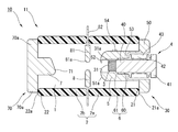
- Example 1 of a field emission device >> The reference numeral 10 in FIGS. 1 and 2 shows an example of an X-ray apparatus to which the electric field emission apparatus of the present embodiment is applied.
- FIG. 4 shows an example of an X-ray apparatus to which the electric field emission apparatus of the present embodiment is applied.
- FIG. 5 detailed description is suitably abbreviate
- FIG. 10 the opening 21 at one end of the cylindrical insulator 2 and the opening 22 at the other end are sealed (e.g., brazed and sealed) by the emitter unit 30 and the target unit 70, respectively.
- a vacuum vessel 11 having a vacuum chamber 1 on the inner wall side of the insulator 2 is configured.
- the transverse direction of the vacuum chamber 1 (direction intersecting with both end directions; hereinafter, referred to simply as the transverse direction) And a grid electrode 8 extending to.
- the insulator 2 is made of, for example, an insulating material such as ceramic, and can insulate the emitter unit 30 (emitter 3 described later) and the target unit 70 (target 7 described later) from each other and form the vacuum chamber 1 inside Therefore, various forms can be applied.
- the grid electrode 8 for example, a lead terminal 82 described later
- the both may be soldered or the like And those assembled and configured with each other.
- the emitter unit 30 includes an emitter 3 having an electron generation unit 31 at a portion facing the target unit 70 (target 7 described later), and a movable body 40 movable in both end directions.
- Movable emitter supporting portion 4 movably supporting 3 in both end directions of vacuum chamber 1, guard electrode 5 positioned on the outer peripheral side of electron generating portion 31 of emitter 3, and both end directions of moving body 40
- a movement restricting portion 6 which restricts the movement to the other end side (the target 7 side described later) among the movement of.
- the emitter 3 has the electron generating unit 31 as described above, and various kinds of emitters can be used as long as they can generate electrons from the electron generating unit 31 by voltage application and can emit the electron beam L1 as illustrated (radiant). It is possible to apply the form of As a specific example, for example, a material such as carbon (carbon nanotube etc.) is used, and it is possible to apply the emitter 3 which is shaped like a block as shown or vapor deposited in a thin film shape. . In the electron generation unit 31, it is preferable to make the surface of the side facing the target unit 70 (target 7 described later) concave (curved) to facilitate focusing of the electron beam L1.
- the emitter support 4 is provided with a movable body 40 movable in both end directions, and can support the emitter 3 movably in both end directions via the movable body 40 as described above. If it is, it is possible to apply various forms.
- a flange portion 41 is formed in a columnar shape extending in both end directions inside the guard electrode 5 on one end side (opening 21 side) of the columnar shape, and the emitter 3 is supported on the other end side (opening 22 side)
- the movable body 40 which adheres and supports the opposite side of the electron generating portion 31 in the emitter 3 by caulking or welding etc., and the support in the vacuum container 11 which can extend and contract in both end directions (for example, as shown in FIG.
- a protruding portion 60 which is a part of an element constituting the movement restricting portion 6 described later is formed so as to protrude laterally outward from the outer peripheral side of the movable body 40. It is good.
- the moving body 40 moves in both end directions by the expansion and contraction of the bellows 42, and as a result, the emitter 3 also moves in both end directions.
- the emitter supporting portion 4 can be configured by applying various materials, and is not particularly limited.
- a conductive metal material such as stainless steel (SUS material etc.) or copper is used. The ones that were
- bellows 42 As the bellows 42, as long as it can be expanded and contracted in the both end directions as described above, various forms can be applied, and examples thereof include those formed by appropriately processing a thin plate-like metal material or the like. As a specific example, as shown in the drawing, a configuration having a bellows-like cylindrical wall 43 extending in both end directions so as to surround the outer peripheral side of the moving body 40 can be mentioned.
- one end is attached to the flange portion 41 of the moving body 40 by brazing or the like, and the other end is soldered to the inside of the guard electrode 5 (step portion 53 described later in the figure).
- the vacuum chamber 1 and the atmosphere side can be separated by attachment or the like so that the vacuum chamber 1 can be airtightly held, but the present invention is not limited to this.
- one end of the bellows 42 is supported by the emitter support 4 (for example, supported by the movable body 40 or the flange portion 41), and the other end is supported by the vacuum vessel 11 (for example, inside the guard electrode 5 or by the flange 50 described later)
- the vacuum vessel 11 for example, inside the guard electrode 5 or by the flange 50 described later
- the guard electrode 5 is provided so as to be located on the outer peripheral side of the electron generation unit 31 of the emitter 3 as described above, and the electron generation unit 31 of the emitter 3 moved by the movement of the emitter support 4 is When the distance between the guard electrode 5 and the emitter 3 is shortest (close or in contact state; for example, the state shown in FIG. 1), the electron beam L1 emitted from the emitter 3 Various forms can be applied as long as dispersion can be suppressed.
- the guard electrode 5 for example, a material such as stainless steel (SUS material or the like) is used, and it is a cylindrical shape extending in both end directions of the vacuum chamber 1 on the outer peripheral side of the emitter 3. It is supported by the end face 21a of the opening 21 of the insulator 2 through the formed flange portion 50, and the other end side (that is, the target 7 side to be described later) in the both end direction contacts and separates with the emitter 3.
- SUS material stainless steel
- the configuration of the guard electrode 5 in contact with and separated from the emitter 3 is not particularly limited.
- the small diameter portion 51 may be formed on the other end side in both end directions, but as shown in FIGS. 1 and 2, it extends inside in the transverse direction of the vacuum chamber 1
- an edge 52 intersecting with the peripheral edge 31 a of the electron generating portion 31 of the emitter 3 is formed in both end directions of the vacuum chamber 1.
- the structure (illustration omitted) which formed both the small diameter part 51 and the edge 52 is mentioned.
- the emitter 3 moves in both directions on the inner side (cylindrical inner wall side) of the guard electrode 5 by the movement of the emitter support 4, and the electron generation of the emitter 3
- the portion 31 contacts or separates the small diameter portion 51 or the edge portion 52. Further, in the case of the configuration provided with the edge 52, when the emitter 3 approaches or contacts the guard electrode 5, the peripheral edge 31a of the electron generation unit 31 is covered and protected by the edge 52. become.
- a stepped portion 53 is formed inside the guard electrode 5 by a shape that is reduced in a stepwise manner from one end side toward the other end side.
- the crossing portion 61 which is a part of the elements constituting the movement restricting portion 6 described later is the inside in the transverse direction from the inside of the guard electrode 5.
- the electron generating portion 31 of the emitter 3 is directed toward the small diameter portion 51 or the edge portion 52 according to the shape reduced in diameter from one end side toward the other end side. While being guided, it also moves inside the guard electrode 5. Further, as in the case of the guard electrode 5 in the figure, if the bellows 42 can be accommodated inside the guard electrode 5, the impact or the like from the outer peripheral side of the vacuum vessel 11 to the bellows 42 is suppressed (the bellows 42 is protected It becomes possible to control the damage etc.). Furthermore, it can contribute to the miniaturization of the X-ray apparatus 10.
- the apparent radius of curvature of the peripheral portion 31a of the electron generating portion 31 of the emitter 3 is made large, and local electric field concentration that may occur in the electron generating portion 31 (particularly, the peripheral portion 31a) is suppressed. It can be mentioned to have a shape that can suppress the occurrence of a flash from the generation part 31 to another part. For example, as in the guard electrode 5 shown in the drawing, a shape having a convex curved surface portion 51a on the other end side in the both end directions can be mentioned.
- the getter 54 is attached to the outer peripheral side by welding or the like, but the attachment position, material, and the like of the getter 54 are not particularly limited.
- the movement restricting portion 6 can restrict movement of the movable body 40 toward the other end in movement in both end directions, and the position where the movable body 40 is in the movement restricted state is the discharge position of the emitter.
- Various configurations can be applied as long as the configuration can be set to the position.
- the configuration formed inside the vacuum chamber 1 like the movement restricting portion 6 in the figure is formed on the outer peripheral side of the moving body 40 (formed between the emitter 3 and the flange portion 41 in the figure)
- a flange-like protruding portion 60 protruding outward in the transverse direction from the outer peripheral side, and the cylindrical inner peripheral side of the guard electrode 5 (formed between the edge 52 and the step portion 53 in the drawing)
- a step-like crossing portion 61 projecting inward in the transverse direction from the circumferential side, wherein the crossing portion 61 is a position on the other end side of the vacuum chamber 1 relative to the projecting portion 60 in both end directions
- the structure formed in the position which intersects with the projection part 60 is mentioned, it is not limited to this.
- the projecting portion 60 is formed to project laterally outward from the outer peripheral side of the flange portion 41, and the intersecting portion 61 is formed to project laterally inward from the inside of the flange portion 50 (from the projecting portion 60 Even if the movement restricting portion 6 is formed outside the vacuum chamber 1 (not shown), the projecting portions 60 and the intersecting portions 61 cross each other. As long as the movable body 40 is in the movement restriction state and the movement restriction state is in contact with the movable body 40, the position where the movement restriction state is the discharge restriction position of the emitter 3 can be set.
- the emitter 3 in order to configure the emitter 3 to be in the discharge position when the projecting portion 60 and the intersecting portion 61 abut, it is possible to appropriately set the positions where the projecting portion 60 and the intersecting portion 61 are formed.
- the distance between the protruding portion 60 and the electron generating portion 31 of the emitter 3 in the both end direction is both ends between the crossing portion 61 and the edge 52
- the position where the protrusion 60 and the intersection 61 are formed may be appropriately set so as to be equal to or less than the distance in the direction.
- the target unit 70 includes the target 7 facing the electron generating portion 31 of the emitter 3 and the flange portion 70 a supported by the end face 22 a of the opening 22 of the insulator 2.
- the target 7 various forms can be applied as long as the electron beam L 1 emitted from the electron generation unit 31 of the emitter 3 collides to emit the X-ray L 2 or the like as illustrated. .
- an inclined surface 71 extending in a cross direction which is inclined at a predetermined angle with respect to the electron beam L1 is formed at a portion of the emitter facing the electron generating portion 31.
- the X-ray L2 is irradiated in a direction bent from the irradiation direction of the electron beam L1 (for example, in the cross sectional direction of the vacuum chamber 1 as illustrated). become.
- the distance between the electron generation unit 31 of the emitter 3 and the target 7 can be changed by appropriately operating the emitter support 4. For example, as shown in FIG. 2, if the electron generation unit 31 is moved from the discharge position to the non-discharge position and electric field emission is suppressed, desired modification of the guard electrode 5, target 7, grid electrode 8, etc. Processing becomes possible. Further, for example, compared with the conventional device provided with the above-described large-diameter exhaust pipe, it is easy to miniaturize, and it is possible to reduce the number of manufacturing steps and the product cost.
- a desired voltage for modification is appropriately set between the guard electrode 5 and the grid electrode 8 (extraction terminal 82 etc.), between the target 7 and the grid electrode 8, etc.
- the voltage By applying the voltage, the discharge is repeated in the guard electrode 5 or the like, and the guard electrode 5 or the like is subjected to a modification process (for example, the surface of the guard electrode 5 is dissolved and smoothed).
- the emitter support 4 is operated again to move the emitter 3 toward the opening 22 (move to the discharge position) as shown in FIG. Put in a state.
- the distance between the electron generating portion 31 of the emitter 3 and the edge portion 52 of the guard electrode 5 becomes close to or in contact with each other, and the distance between the both becomes shortest, and the dispersion of the electron beam L1 emitted from the emitter 3 It will be in the state which can be controlled.
- the movement restricting part 6 the projecting part 60 and the crossing part 61 cross each other and abut, and the moving body 40 is put into the movement restriction state, so that the movement of the emitter supporting part 4 (movement in one end side direction) is suppressed.
- the emitter 3 is suppressed from moving to the target side beyond the discharge position. Furthermore, even in the case where both of the electron generating portion 31 and the edge portion 52 are in contact with each other, the contact pressure is suppressed low by the movement restricting portion 6.
- the electron generator 31 of the emitter 3 and the guard electrode 5 have the same potential, for example, apply a desired voltage between the emitter 3 and the target 7.
- a desired voltage between the emitter 3 and the target 7. electrons are generated from the electron generation unit 31 of the emitter 3 to emit the electron beam L1, and when the electron beam L1 collides with the target 7, the X-ray L2 is emitted from the target 7.
- the reforming process as described above can suppress the flash phenomenon (generation of electrons) from the guard electrode 5 in the X-ray apparatus 10, and can stabilize the electron generation amount of the X-ray apparatus 10 .
- the electron beam L1 can be made into a focusing type electron flux, the focal point of the X-ray L2 can be easily converged, and high fluoroscopic resolution can be obtained.
- the electric field emission device of the present invention may be configured to be able to cool the electric field emission device by using a cooling function when heat is generated by collision of an electron beam to a target or the like.
- the cooling function may be applied to various methods such as air cooling, water cooling, oil cooling and the like.
- the cooling function of the oil cooling system for example, a configuration in which the field emission device is immersed in cooling oil in a predetermined container may be mentioned, and defoaming treatment of the cooling oil in the immersion state (vacuum pump It is also possible to appropriately carry out a process using an etc.).
- each element (insulator, emitter unit, target unit etc.) constituting the vacuum vessel may be integrally brazed.
- Various methods can be applied as long as the chamber can be kept airtight (high vacuum etc.).
- the vacuum pressure of the vacuum chamber acts, but the emitter can be supported movably in the both end directions of the vacuum chamber by appropriately performing the operation related to each support, and the movement is restricted.
- Various modes can be applied as long as the mobile unit is in a movement restricted state by the unit.
- the emitter support portion is operated and the moderation feeling (click feeling) is obtained when the emitter moves to a desired position (discharge position etc.), the desired position is grasped when the emitter support portion is operated.
- the fixing means capable of appropriately fixing the emitter in the desired position, the external force (for example, the structure having the above-mentioned oil cooling type cooling function) In this case, even if the suction force of a vacuum pump that can act on the support during the defoaming treatment of the cooling oil acts), the emitter can be prevented from moving from the desired position, and the field emission device It is possible to contribute so that each of the field emission and the modification process of the guard electrode etc. can be realized appropriately.
- the fixing means is not particularly limited, and various fixing means can be applied. If the above-mentioned X-ray apparatus 10 is taken as an example, movement of the emitter support 4 in both end directions is described. The stopper which can be fixed by screwing etc. is mentioned.
Landscapes
- Engineering & Computer Science (AREA)
- Manufacturing & Machinery (AREA)
- X-Ray Techniques (AREA)
- Cold Cathode And The Manufacture (AREA)
Abstract
真空室(1)においてエミッタ(3)およびターゲット(7)を互いに対向して配置し、エミッタ(3)の電子発生部(31)の外周側には、ガード電極(5)を備える。エミッタ(3)は、真空室(1)の両端方向に移動自在な移動体(40)を有したエミッタ支持部(4)により、当該両端方向に対し移動自在に支持する。ガード電極(5)の改質処理は、エミッタ支持部(4)を操作し、エミッタ(3)を無放電位置に移動して、電子発生部(31)の電界放射を抑制した状態にし、ガード電極(5)に電圧を印加し放電を繰り返して行う。改質処理の後は、再びエミッタ支持部(4)を操作し、エミッタ(3)を放電位置に移動し、移動規制部(6)により移動体(40)の真空室(1)の他端側への移動を規制した状態で、電子発生部(31)の電界放射を可能な状態にする。
Description
本発明は、X線装置,電子管,照明装置等の種々の機器に適用される電界放射装置および改質処理方法に関するものである。
X線装置,電子管,照明装置等の種々の機器に適用される電界放射装置の一例としては、真空容器の真空室において互いに対向した方向に位置(所定距離隔てて位置)するエミッタ(炭素等を用いてなる電子源)とターゲットとの間に電圧印加し、エミッタの電界放射(電子を発生させて放出)によって電子線を放出し、その放出した電子線をターゲットに衝突させて所望の機能(例えばX線装置の場合はX線の外部放出による透視分解能)を発揮する構成が知られている。
また、例えば、エミッタとターゲットとの間にグリッド電極等を介在させて3極管構造としたり、エミッタの電子発生部(ターゲットに対向する側に位置し電子を発生する部位)の表面を曲面状にしたり、エミッタと同電位のガード電極を当該エミッタの外周側に配置する等により、エミッタから放出される電子線の分散を抑制することが検討されている(例えば特許文献1,2)。
前述のような電圧印加により、エミッタの電子発生部のみから電子を発生させて電子線を放出することが望ましいが、真空室内に不要な微小突起や汚れ等が存在していると、意図しない閃絡現象を起こし易くなり、耐電圧性等が得られず、所望の機能を発揮できなくなる虞がある。
例えば真空室内のガード電極等(ターゲット,グリッド電極,ガード電極等;以下、単にガード電極等と適宜称する)において、局部的な電界集中を起こし易い部位が形成(例えば加工において形成された微小突起等)されている場合、ガス成分(例えば真空容器内に残存するガス成分)を吸着している場合、電子を発生させ易い元素が含まれている場合(適用する材料中に含まれている場合)等が挙げられる。このような場合、例えばガード電極にも電子発生部が形成され、電子の発生量が不安定になり、電子線が分散し易くなり、例えばX線装置の場合にはX線等の焦点はずれ等を起こす虞もある。
そこで、閃絡現象の抑制を図る手法(電子の発生量を安定化させる手法)として、例えばガード電極等に電圧(高電圧等)を印加(例えばガード電極とグリッド電極に印加)し放電を繰り返す電圧放電コンディショニング処理(改質(再生);以下、単に改質処理と適宜称する)を施す手法が検討されている。
しかしながら、前述のような改質処理の電圧を単にガード電極等に印加すると、エミッタの電界放射(例えば改質処理が行われる前に電界放射)も起こり易く、当該ガード電極等が十分に改質処理されない虞がある。
本発明は、かかる技術的課題を鑑みてなされたものであって、エミッタの電界放射を抑制しながらガード電極等の改質処理を行うことができ、電界放射装置の特性の向上に貢献可能な技術を提供することにある。
この発明に係る電界放射装置,改質処理方法は、前記の課題を解決できるものである。電界放射装置の一態様は、筒状の絶縁体の両端側が封止されて当該絶縁体の内壁側に真空室が形成された真空容器と、真空室の一端側に位置し、当該真空室の他端側に対向する電子発生部を有したエミッタと、エミッタの電子発生部の外周側に位置しているガード電極と、真空室の他端側に位置し、エミッタの電子発生部に対向して設けられたターゲットと、両端方向に移動自在な移動体を有し、当該移動体を介してエミッタを真空室の両端方向に対し移動自在に支持する可動自在なエミッタ支持部と、移動体の両端方向の移動のうち真空室の他端側への移動を規制する移動規制部と、を備え、エミッタ支持部の可動により、エミッタの電子発生部とターゲットとの間の距離が変化し、移動規制部により移動体の真空室の他端側への移動が規制された状態で、エミッタの電子発生部が電界放射することを特徴とする。
また、移動規制部は、移動体の外周側から真空室の横断方向外側に突出した突出部と、突出部よりも真空室の他端側の位置であって両端方向において当該突出部と交叉している位置に設けられた交叉部と、を備え、突出部と交叉部とが当接して、移動体の真空室の他端側への移動が規制されるものでも良い。
また、ガード電極は、真空室の両端方向に延在した筒状であり、一端が真空容器に支持され、交叉部は、ガード電極の筒状内周側(の中央部)から真空室の横断方向内側に突出して形成されているものでも良い。
また、移動規制部により移動体の真空室の他端側への移動が規制された状態で、ガード電極のターゲット側とエミッタの電子発生部との距離が最短となるものでも良い。
また、ガード電極のターゲット側に、小径部が形成されているものでも良い。また、ガード電極のターゲット側に、真空室の横断方向に延出して当該真空室の両端方向においてエミッタの電子発生部の周縁部と交叉する縁部が形成されているものでも良い。
また、真空室の両端方向に伸縮自在なベローズを有し、そのベローズの一端側がエミッタ支持部に支持され、他端側が真空容器に支持されているものでも良い。また、移動体は、エミッタの電子発生部の反対側において両端方向に延在した形状であっても良い。また、真空室のエミッタとターゲットとの間に、グリッド電極が設けられているものでも良い。
前述の電界放射装置の改質処理方法の一態様としては、エミッタ支持部の操作によりエミッタの電子発生部とガード電極との両者を互いに離反した状態で、ガード電極に電圧を印加して、真空室内の少なくともガード電極を改質処理することを特徴とする。
以上示したように本発明によれば、エミッタの電界放射を抑制しながらガード電極等の改質処理を行うことができ、電界放射装置の特性の向上に貢献可能となる。
本発明の実施形態における電界放射装置は、絶縁体の両端側が封止されて形成された真空室において、単に、互いに対向して位置するエミッタおよびターゲットを備えたり、エミッタの電子発生部の外周側にガード電極を備えた構成とするのではなく、真空室の両端方向(以下、単に両端方向と適宜称する)に移動自在な移動体を介してエミッタを当該両端方向に対し移動自在に支持する可動自在なエミッタ支持部を備え、そのエミッタ支持部の可動によりエミッタの電子発生部とターゲットとの間の距離を変化できるように構成したものである。また、移動体の両端方向の移動のうち真空室の他端側(ターゲット側)への移動を規制する移動規制部を備えたものであり、当該移動規制部により移動体の真空室の他端側への移動を規制した状態(以下、単に移動規制状態と適宜称する)で、エミッタの電子発生部が電界放射するように構成したものである。
従来、ガード電極等を改質処理する手法としては、前述のようにガード電極等に対し単に高電圧を印加する手法の他に、ガード電極等を真空雰囲気下で放置し吸着ガスを取り除く手法が知られている。この手法は、例えば、真空容器に大口径排気管を設けて電界放射装置(以下、従来装置と称する)を構成し、その大口径排気管を介して当該真空室を高温真空状態にすることにより、当該真空室のガード電極等の吸着ガスを放出し、その後、当該真空室を大気雰囲気下に戻し大口径排気管を介して当該真空室内にエミッタ等を配置し、当該真空室を封止し再度真空状態にする手法である。
しかしながら、前述のような大口径排気管を設けた真空容器において、真空室の高温真空状態を長時間保つことは困難であり、再度真空状態にするまでの間にガスがガード電極等に再吸着する虞もあり、ガード電極等に形成された粗い表面については改質(滑らかに)することができない。また、大口径排気管により、真空容器が大型化し、製造工数の増加や製品コストの上昇を招くことも考えられる。
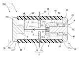
一方、本実施形態のような電界放射装置の構成によれば、前述の従来手法を適用しなくてもガード電極等の改質処理を行うことが可能となる。当該改質処理を行う場合、エミッタ支持部を操作して、エミッタを放電位置(電界放射する位置)から無放電位置(放電電界以下)に移動(電子発生部とターゲットとの間の距離を長くする方向に移動)させることにより、エミッタの電界放射を抑制した状態(例えば後述の図2に示すように、エミッタの電子発生部とガード電極との両者を互いに離反した状態(両者間に隙間を形成))にし、その状態でガード電極等に電圧を印加して改質処理を行うことができ、例えばガード電極等の表面が溶解平滑化されることになる。これにより、所望の耐電圧を得ることが可能となる。また、前述のように電界放射を抑制した状態であれば、改質処理の際にエミッタに対しては負荷が掛からないようにすることができる。
したがって、本実施形態の改質処理によれば、例えばガード電極等の表面に微小突起等が存在していても、その表面を滑らかにすることが可能となる。また、ガス成分(例えば真空容器内に残存するガス成分)を吸着している場合には、当該吸着ガスが放出されることになる。さらに、電子を発生させ易い元素が含まれている場合には、前記の溶解平滑化により、当該元素をガード電極等の内部に留めることができ、当該元素に起因する電子発生を抑制することが可能となる。そして、電界放射装置においては、電子の発生量が安定し易くなる。
前述のようにガード電極等を改質処理した後は、再びエミッタ支持部を操作し、エミッタを無放電位置から放電位置に移動(電子発生部とターゲットとの間の距離を短くする方向に移動)させることにより、エミッタの電子発生部とガード電極との間の距離を最短の状態(エミッタの電子発生部とガード電極とが近接または接触した状態)にすることができる。そして、エミッタ(電子発生部)の電界放射が可能な状態となり、電界放射装置の所望の機能を発揮(X線装置の場合はX線照射等)できることになる。
また、エミッタが放電位置に位置している場合、エミッタ支持部の移動体が移動規制部によって移動規制状態、すなわちエミッタ支持部の可動(一端側方向の可動)が抑制された状態となり、エミッタにおいては放電位置を越えてターゲット側に移動しないように抑制された状態となる。したがって、本実施形態によれば、エミッタの放電位置を、移動体が移動規制状態となる位置に設定することにより、エミッタ支持部の操作によりエミッタの電子発生部とターゲットとの間の距離を変化させる場合に、放電位置(またはガード電極)に対するエミッタの位置決めが容易となる。
ここで、前述のような移動規制部を持たない装置、例えば図4,図5に示すように単にエミッタ支持部4等を備え、エミッタ3の電子発生部31の周縁部31aと交叉する縁部52等がガード電極5に形成されている装置10Aに着目すると、当該エミッタ支持部4を操作し図4に示すようにエミッタ3が放電位置に移動してガード電極5と接触(図4では交叉するように接触)した場合、その接触面には真空室1の真空圧力が掛かることが考えられる。この真空圧力により、接触面に掛かる接触圧力が大きくなってしまう場合には、当該エミッタ3(電子発生部31等)やガード電極5(縁部52等)には応力が発生し易く、各々の形状が変形したり、電界放射装置の所望の特性を保持できなくなることが考えられる。
一方、本実施形態に係る電界放射装置(例えば後述のX線装置10)は、前述のようにエミッタの放電位置を移動体の移動規制状態となる位置に設定することができる構成であるため、たとえ放電位置のエミッタがガード電極と接触する構成であっても、当該接触圧力を低く抑えることができ、当該エミッタやガード電極の形状等の変形を防止し、電界放射装置の所望の特性を保持することが可能となる。
本実施形態の電界放射装置は、前述のようにエミッタを両端方向に対して移動自在に支持するエミッタ支持部や、エミッタ支持部の移動体の移動を規制する移動規制部等を備え、エミッタの電子発生部とターゲットとの間の距離を変化できる構成であれば、例えば各種分野の技術常識を適宜適用する等により、多彩な変更が可能なものであって、その一例として以下に示すものが挙げられる。
≪電界放射装置の実施例1≫
図1,図2の符号10は、本実施形態の電界放射装置を適用したX線装置の一例を示すものである。なお、図4,図5と同様のものについては、それぞれ同一に符号を用いる等により、詳細な説明を適宜省略する。X線装置10においては、筒状の絶縁体2の一端側の開口21と他端側の開口22とが、それぞれエミッタユニット30とターゲットユニット70とにより封止(例えば蝋付けして封止)されて、絶縁体2の内壁側に真空室1を有した真空容器11が構成されている。エミッタユニット30(後述のエミッタ3)とターゲットユニット70(後述のターゲット7)との間には、当該真空室1の横断方向(両端方向に対して交差する方向;以下、単に横断方向と適宜称する)に延在するグリッド電極8が設けられている。
図1,図2の符号10は、本実施形態の電界放射装置を適用したX線装置の一例を示すものである。なお、図4,図5と同様のものについては、それぞれ同一に符号を用いる等により、詳細な説明を適宜省略する。X線装置10においては、筒状の絶縁体2の一端側の開口21と他端側の開口22とが、それぞれエミッタユニット30とターゲットユニット70とにより封止(例えば蝋付けして封止)されて、絶縁体2の内壁側に真空室1を有した真空容器11が構成されている。エミッタユニット30(後述のエミッタ3)とターゲットユニット70(後述のターゲット7)との間には、当該真空室1の横断方向(両端方向に対して交差する方向;以下、単に横断方向と適宜称する)に延在するグリッド電極8が設けられている。
絶縁体2は、例えばセラミック等の絶縁材料を用いて成り、エミッタユニット30(後述のエミッタ3)とターゲットユニット70(後述のターゲット7)とを互いに絶縁し、内部に真空室1を形成できるものであれば、種々の形態を適用することができる。例えば、図示するように同心状に配置された2つの円筒状の絶縁部材2a,2bの両者間にグリッド電極8(例えば後述の引出端子82)を介在させた状態で、当該両者を蝋付け等により互いに組み付けて構成されたものが挙げられる。
エミッタユニット30は、ターゲットユニット70(後述するターゲット7)に対向する部位に電子発生部31を有したエミッタ3と、両端方向に移動自在な移動体40を有し当該移動体40を介してエミッタ3を真空室1の両端方向に対し移動自在に支持する可動自在なエミッタ支持部4と、エミッタ3の電子発生部31の外周側に位置しているガード電極5と、移動体40の両端方向の移動のうち他端側(後述するターゲット7側)への移動を規制する移動規制部6と、を備えている。
エミッタ3においては、前述のように電子発生部31を有し、電圧印加により電子発生部31から電子を発生し、図示するように電子線L1を放出できるもの(放射体)であれば、種々の形態を適用することが可能である。具体例としては、例えば炭素等(カーボンナノチューブ等)の材料を用いてなるものであって、図示するように塊状に成形された、または薄膜状に蒸着させたエミッタ3を適用することが挙げられる。電子発生部31においては、ターゲットユニット70(後述するターゲット7)に対向する側の表面を凹状(曲面状)にして、電子線L1を集束し易くすることが好ましい。
エミッタ支持部4においては、両端方向に移動自在な移動体40を備えたものであって、移動体40を介して、前述のようにエミッタ3を両端方向に対して移動自在に支持できるものであれば、種々の形態を適用することが可能である。具体例としては、ガード電極5の内側において両端方向に延在した柱状で当該柱状一端側(開口21側)にフランジ部41が形成され他端側(開口22側)にてエミッタ3を支持(例えば、エミッタ3における電子発生部31の反対側を、かしめや溶着等により固着して支持)する移動体40と、両端方向に伸縮自在で真空容器11に支持(例えば図示するようにガード電極5を介して絶縁体2に支持)されたベローズ42と、を備えた構成が挙げられる。また、移動体40においては、後述の移動規制部6を構成する要素の一部である突出部60が、当該移動体40の外周側から横断方向外側に突出するように形成された構成であっても良い。
このように移動体40,ベローズ42を備えたエミッタ支持部4の場合、ベローズ42の伸縮により移動体40が両端方向に移動し、その結果、エミッタ3も両端方向に移動することになる。また、エミッタ支持部4は、種々の材料を適用して構成することができ、特に限定されるものではないが、例えばステンレス(SUS材等)や銅等のように導電性の金属材料を用いたものが挙げられる。
ベローズ42は、前述のように両端方向に伸縮自在なものであれば、種々の形態を適用することが可能であり、例えば薄板状金属材料等を適宜加工して成形されたものが挙げられる。具体例としては、図示するように、移動体40の外周側を包囲するように両端方向に延在する蛇腹状筒壁43を有した構成が挙げられる。
また、図中のベローズ42の支持構成の場合、一端側が移動体40のフランジ部41に蝋付け等により取り付けられ、他端側がガード電極5の内側(図中では後述の段差部53)に蝋付け等により取り付けられて、真空室1と大気側(真空容器11外周側)とを区分し当該真空室1を気密に保持できる構成となっているが、これに限定されるものではない。すなわち、ベローズ42の一端側がエミッタ支持部4に支持(例えば移動体40やフランジ部41に支持)され、他端側が真空容器11に支持(例えばガード電極5の内側や後述のフランジ部50に支持)され、前述のように両端方向に伸縮自在であって、真空室1と大気側(真空容器11外周側)とを区分し当該真空室1を気密に保持できる構成(真空容器11の一部を形成する構成)であれば、種々の形態を適用することが可能である。
ガード電極5においては、前述のようにエミッタ3の電子発生部31の外周側に位置するように設けられたものであって、エミッタ支持部4の可動によって移動するエミッタ3の電子発生部31が接離し、当該ガード電極5とエミッタ3との間の距離が最短となった状態(近接または接触した状態;例えば図1に示す状態)の場合に、当該エミッタ3から放出される電子線L1の分散を抑制できるものであれば、種々の形態を適用することが可能である。
ガード電極5の具体例としては、例えばステンレス等(SUS材等)の材料を用いてなり、エミッタ3の外周側で真空室1の両端方向に延在した筒状で、両端方向の一端側に形成されたフランジ部50を介して絶縁体2の開口21の端面21aに支持され、当該両端方向の他端側(すなわち後述のターゲット7側)がエミッタ3と接離する構成が挙げられる。
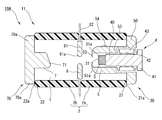
このガード電極5のエミッタ3と接離する構成は、特に限定されるものではない。例えば図3に示すように両端方向の他端側に小径部51を形成した構成であっても良いが、図1,図2に示したように、真空室1の横断方向内側に延出し当該真空室1の両端方向においてエミッタ3の電子発生部31の周縁部31aと交叉する縁部52が形成された構成も挙げられる。また、小径部51および縁部52の両方を形成した構成(図示省略)も挙げられる。
このような接離構成のガード電極5を備えた場合、エミッタ支持部4の可動により、エミッタ3が当該ガード電極5の内側(筒状内壁側)において両端方向に移動し、エミッタ3の電子発生部31が小径部51あるいは縁部52に接離することになる。また、縁部52を備えた構成の場合には、当該ガード電極5にエミッタ3が近接または接触する場合に、電子発生部31の周縁部31aが、縁部52よって覆われて保護されることになる。
図中のガード電極5の場合、一端側から他端側に近づくに連れて階段状に縮径された形状により、当該ガード電極5の内側に段差部53が形成されている。このような段差部53に前記ベローズ42の他端側を取り付けることにより、当該取付作業が容易となり、その取付構造も安定したものとなる。なお、図中のガード電極5の内側においては、段差部53の他に、後述の移動規制部6を構成する要素の一部である交叉部61が、当該ガード電極5の内側から横断方向内側に突出するように形成(突出部60と交叉するように形成)されている。
また、図中のガード電極5のように一端側から他端側に近づくに連れて縮径された形状によれば、エミッタ3の電子発生部31が、小径部51あるいは縁部52に向かって案内されながら、ガード電極5の内側を移動することにもなる。また、図中のガード電極5のように、当該ガード電極5の内側にベローズ42を収容できる構成であれば、そのベローズ42に対する真空容器11の外周側からの衝撃等を抑制(ベローズ42を保護し損傷等を抑制)することが可能となる。さらに、X線装置10の小型化にも貢献できる。
また、エミッタ3の電子発生部31の周縁部31aの見かけ上の曲率半径を大きくなるようにし、電子発生部31(特に周縁部31a)で起こり得る局部的な電界集中を抑制したり、その電子発生部31から他の部位に対する閃絡を抑制できる形状とすることが挙げられる。例えば、図示するガード電極5のように、両端方向の他端側に凸の曲面部51aを有した形状が挙げられる。
なお、図中のガード電極5の場合、外周側にゲッター54が溶接等により取り付けられているが、そのゲッター54の取付位置や材質等は特に限定されるものではない。
移動規制部6においては、前述のように移動体40の両端方向の移動のうち他端側への移動を規制でき、当該移動体40が移動規制状態となる位置を、エミッタの放電位置となる位置に設定できる構成であれば、種々の形態を適用することが可能である。
図中の移動規制部6のように真空室1内側に形成した構成の具体例としては、移動体40の外周側に形成(図中ではエミッタ3とフランジ部41との間に形成)され当該外周側から横断方向外側に突出したフランジ状の突出部60と、ガード電極5の筒状内周側に形成(図中では縁部52と段差部53との間に形成)され当該筒状内周側から横断方向内側に突出した段差状の交叉部61と、を備えたものであって、交叉部61が、突出部60よりも真空室1の他端側の位置であって両端方向において当該突出部60と交叉している位置に形成された構成が挙げられるが、これに限定されるものではない。
例えば、突出部60を、フランジ部41の外周側から横断方向外側に突出するように形成し、交叉部61を、フランジ部50の内側から横断方向内側に突出するように形成(突出部60よりも真空室1の他端側の位置に形成)して、移動規制部6を真空室1外側に構成(図示省略)した場合であっても、それら突出部60,交叉部61が互いに交叉して当接し移動体40が移動規制状態となり、その移動規制状態となる位置がエミッタ3の放電位置となる位置に設定できる構成であれば良い。
また、突出部60と交叉部61とが当接する場合にエミッタ3が放電位置となるように構成するには、突出部60,交叉部61が形成される位置を適宜設定することが挙げられる。例えば、図中のような突出部60,交叉部61の場合、突出部60とエミッタ3の電子発生部31との間における両端方向の距離が、交叉部61と縁部52との間における両端方向の距離以下となるように、突出部60,交叉部61が形成される位置を適宜設定することが挙げられる。
次に、ターゲットユニット70は、エミッタ3の電子発生部31に対向するターゲット7と、絶縁体2の開口22の端面22aに支持されるフランジ部70aと、を備えている。
ターゲット7においては、エミッタ3の電子発生部31から放出された電子線L1が衝突し、図示するようにX線L2等を放出できるものであれば、種々の形態を適用することが可能である。図中のターゲット7においては、エミッタの電子発生部31に対向する部位に、電子線L1に対して所定角度で傾斜する交差方向に延在した傾斜面71が形成されている。この傾斜面71に電子線L1が衝突することにより、X線L2は、電子線L1の照射方向から折曲した方向(例えば図示するように真空室1の横断面方向)に、照射されることになる。
グリッド電極8においては、前述のようにエミッタ3とターゲット7との間に介在し、当該グリッド電極8を通過する電子線L1を適宜制御できるものであれば、種々の形態のものを適用することが可能である。例えば図示するように、真空室1の横断方向に延在し電子線L1が通過する通過孔81aを有した電極部(例えばメッシュ状の電極部)81と、絶縁体2を貫通(真空室1横断方向に貫通)する引出端子82と、を備えた構成が挙げられる。
以上示したように構成されたX線装置10によれば、エミッタ支持部4を適宜操作することにより、エミッタ3の電子発生部31とターゲット7との間の距離を変化させることができる。例えば図2に示したように当該電子発生部31が放電位置から無放電位置に移動し電界放射を抑制された状態であれば、ガード電極5,ターゲット7,グリッド電極8等において所望の改質処理が可能となる。また、例えば前述の大口径排気管を設けた従来装置と比較すると、小型化することが容易であり、製造工数の低減や製品コストの低減を図ることも可能となる。
≪X線装置10のガード電極等の改質処理の一例≫
前述のX線装置10のガード電極5等を改質処理する場合、まず、エミッタ支持部4を操作して、図2に示すようにエミッタ3を開口21側に移動(無放電位置に移動)し、電子発生部31の電界放射を抑制した状態にする。この場合、エミッタ3の電子発生部31とガード電極5の縁部52(なお、図3の場合は小径部51)との両者は、互いに離反(エミッタ3を無放電位置(放電電界以下)に移動)した状態となる。この図2に示すような状態であれば、例えばガード電極5とグリッド電極8(引出端子82等)との間や、ターゲット7とグリッド電極8との間などに所望の改質時電圧を適宜印加することにより、ガード電極5等において放電が繰り返され、当該ガード電極5等が改質処理(例えばガード電極5の表面が溶解平滑化)されることになる。
前述のX線装置10のガード電極5等を改質処理する場合、まず、エミッタ支持部4を操作して、図2に示すようにエミッタ3を開口21側に移動(無放電位置に移動)し、電子発生部31の電界放射を抑制した状態にする。この場合、エミッタ3の電子発生部31とガード電極5の縁部52(なお、図3の場合は小径部51)との両者は、互いに離反(エミッタ3を無放電位置(放電電界以下)に移動)した状態となる。この図2に示すような状態であれば、例えばガード電極5とグリッド電極8(引出端子82等)との間や、ターゲット7とグリッド電極8との間などに所望の改質時電圧を適宜印加することにより、ガード電極5等において放電が繰り返され、当該ガード電極5等が改質処理(例えばガード電極5の表面が溶解平滑化)されることになる。
前述の改質処理の後は、再びエミッタ支持部4を操作し、図1に示すようにエミッタ3を開口22側に移動(放電位置に移動)し、電子発生部31の電界放射が可能な状態にする。この場合、エミッタ3の電子発生部31とガード電極5の縁部52との両者が近接または接触することにより、当該両者間の距離が最短となり、エミッタ3から放出される電子線L1の分散を抑制できる状態となる。また、移動規制部6において突出部60および交叉部61が互いに交叉して当接し、移動体40が移動規制状態となるため、エミッタ支持部4の可動(一端側方向の可動)が抑制された状態となり、エミッタ3においては放電位置を越えてターゲット側に移動しないように抑制された状態となる。さらに、電子発生部31と縁部52との両者が接触する場合であっても、移動規制部6により、当該接触圧力は低く抑えられることとなる。
この図1に示すような状態(移動規制状態)で、エミッタ3の電子発生部31とガード電極5とが互いに同電位で、例えばエミッタ3とターゲット7との間に所望の電圧を印加することにより、エミッタ3の電子発生部31から電子が発生して電子線L1が放出され、その電子線L1がターゲット7に衝突することにより、そのターゲット7からX線L2が放出される。
以上示したような改質処理により、X線装置10においてガード電極5からの閃絡現象(電子の発生)を抑制することができ、当該X線装置10の電子発生量を安定させることができる。また、電子線L1を集束形電子束とすることができ、X線L2の焦点も収束し易くなり、高い透視分解能を得ること可能となる。
以上、本発明において、記載された具体例に対してのみ詳細に説明したが、本発明の技術思想の範囲で多彩な変更等が可能であることは、当業者にとって明白なことであり、このような変更等が特許請求の範囲に属することは当然のことである。
例えば、本発明の電界放射装置は、電子線のターゲットへの衝突等により熱を発生する場合には、冷却機能を用いて当該電界放射装置を冷却できる構成としても良い。冷却機能は、空冷,水冷,油冷等の種々の方式のものを適用することが挙げられる。当該油冷方式の冷却機能の場合には、例えば所定容器内の冷却用油中に電界放射装置を浸漬させた構成が挙げられ、また、当該浸漬状態において冷却用油の脱泡処理(真空ポンプ等を用いた処理)等を適宜行うことも挙げられる。
真空容器の真空室を気密(高真空等)に保持するには、当該真空容器を構成する各要素(絶縁体,エミッタユニット,ターゲットユニット等)は一体蝋付けする手法が挙げられるが、当該真空室を気密(高真空等)に保持できるものであれば、種々の手法を適用することが可能である。
エミッタ支持部においては、例えば真空室の真空圧力が作用することになるが、当該各支持部に係る操作を適宜実施することによりエミッタを真空室の両端方向に対し移動自在に支持でき、移動規制部によって移動体が移動規制状態になるものであれば、種々の態様を適用することが可能である。
例えば、エミッタ支持部を操作して、エミッタが所望位置(放電位置等)に移動した場合に節度感(クリック感)が得られる構成であれば、当該エミッタ支持部の操作時に所望位置を把握することが容易になったり、当該エミッタ支持部の操作性が向上する等、種々貢献することが可能となる。
また、前述のように所望位置に位置した状態のエミッタを適宜固定できる固定手段を備えた構成であれば、例えば意に反する外部からの力(前述の油冷方式の冷却機能を備えた構成の場合には、冷却用油の脱泡処理時に支持部に対して作用し得る真空ポンプの吸引力等)が作用したとしても、当該エミッタが所望位置から移動することを抑制でき、電界放射装置による電界放射やガード電極等の改質処理をそれぞれ適確に実現できるように貢献可能となる。この固定手段は、特に限定されるものではなく、種々の態様のものを適用することが可能であるが、前述のX線装置10を例にして説明すると、エミッタ支持部4の両端方向の移動を螺子止め等により固定することが可能なストッパーが挙げられる。
Claims (11)
- 筒状の絶縁体の両端側が封止されて当該絶縁体の内壁側に真空室が形成された真空容器と、
真空室の一端側に位置し、当該真空室の他端側に対向する電子発生部を有したエミッタと、
エミッタの電子発生部の外周側に位置しているガード電極と、
真空室の他端側に位置し、エミッタの電子発生部に対向して設けられたターゲットと、
両端方向に移動自在な移動体を有し、当該移動体を介してエミッタを真空室の両端方向に対し移動自在に支持する可動自在なエミッタ支持部と、
移動体の両端方向の移動のうち真空室の他端側への移動を規制する移動規制部と、を備え、
エミッタ支持部の可動により、エミッタの電子発生部とターゲットとの間の距離が変化し、
移動規制部により移動体の真空室の他端側への移動が規制された状態で、エミッタの電子発生部が電界放射する、電界放射装置。 - 移動規制部は、
移動体の外周側から真空室の横断方向外側に突出した突出部と、
突出部よりも真空室の他端側の位置であって両端方向において当該突出部と交叉している位置に設けられた交叉部と、を備え、
突出部と交叉部とが当接して、移動体の真空室の他端側への移動が規制される、請求項1記載の電界放射装置。 - ガード電極は、真空室の両端方向に延在した筒状であり、一端が真空容器に支持され、
交叉部は、ガード電極の筒状内周側から真空室の横断方向内側に突出して形成されている、請求項2記載の電界放射装置。 - 移動規制部により移動体の真空室の他端側への移動が規制された状態で、ガード電極のターゲット側とエミッタの電子発生部との距離が最短となる、請求項1~3の何れかに記載の電界放射装置。
- 移動規制部により移動体の真空室の他端側への移動が規制された状態で、ガード電極のターゲット側が、エミッタの電子発生部と接触する、請求項4記載の電界放射装置。
- ガード電極のターゲット側に、小径部が形成されている、請求項4または5に記載の電界放射装置。
- ガード電極のターゲット側に、真空室の横断方向に延出して当該真空室の両端方向においてエミッタの電子発生部の周縁部と交叉する縁部が形成されている、請求項4~6の何れかに記載の電界放射装置。
- 真空室の両端方向に伸縮自在なベローズを有し、そのベローズの一端側がエミッタ支持部に支持され、他端側が真空容器に支持されている、請求項1~7の何れかに記載の電界放射装置。
- 移動体は、エミッタの電子発生部の反対側において両端方向に延在した形状である、請求項1~8の何れかに記載の電界放射装置。
- 真空室のエミッタとターゲットとの間に、グリッド電極が設けられている、請求項1~9の何れかに記載の電界放射装置。
- 請求項1~10の何れかに記載の電界放射装置の改質処理方法であって、
エミッタ支持部の操作によりエミッタの電子発生部とガード電極との両者を互いに離反した状態で、ガード電極に電圧を印加して、真空室内の少なくともガード電極を改質処理する、電界放射装置の改質処理方法。
Priority Applications (3)
| Application Number | Priority Date | Filing Date | Title |
|---|---|---|---|
| KR1020197000572A KR101988529B1 (ko) | 2016-06-23 | 2017-03-16 | 전계 방사 장치 및 개질 처리 방법 |
| CN201780038629.7A CN109314028B (zh) | 2016-06-23 | 2017-03-16 | 场发射装置和重整处理方法 |
| US16/311,985 US10424457B2 (en) | 2016-06-23 | 2017-03-16 | Field emission device and reforming treatment method |
Applications Claiming Priority (2)
| Application Number | Priority Date | Filing Date | Title |
|---|---|---|---|
| JP2016124149A JP6206546B1 (ja) | 2016-06-23 | 2016-06-23 | 電界放射装置および改質処理方法 |
| JP2016-124149 | 2016-06-23 |
Publications (1)
| Publication Number | Publication Date |
|---|---|
| WO2017221478A1 true WO2017221478A1 (ja) | 2017-12-28 |
Family
ID=59997765
Family Applications (1)
| Application Number | Title | Priority Date | Filing Date |
|---|---|---|---|
| PCT/JP2017/010550 Ceased WO2017221478A1 (ja) | 2016-06-23 | 2017-03-16 | 電界放射装置および改質処理方法 |
Country Status (5)
| Country | Link |
|---|---|
| US (1) | US10424457B2 (ja) |
| JP (1) | JP6206546B1 (ja) |
| KR (1) | KR101988529B1 (ja) |
| CN (1) | CN109314028B (ja) |
| WO (1) | WO2017221478A1 (ja) |
Families Citing this family (7)
| Publication number | Priority date | Publication date | Assignee | Title |
|---|---|---|---|---|
| JP6206541B1 (ja) | 2016-06-13 | 2017-10-04 | 株式会社明電舎 | 電界放射装置および改質処理方法 |
| JP6226033B1 (ja) * | 2016-06-24 | 2017-11-08 | 株式会社明電舎 | 電界放射装置および電界放射方法 |
| JP6753498B1 (ja) * | 2019-09-19 | 2020-09-09 | 株式会社明電舎 | エミッタ支持構造及び電界放射装置 |
| JP7400509B2 (ja) * | 2020-02-04 | 2023-12-19 | ヤマハ株式会社 | フェーダ装置 |
| JP7060040B2 (ja) * | 2020-06-05 | 2022-04-26 | 株式会社明電舎 | 電界放射装置および電界放射方法 |
| JP6927368B1 (ja) * | 2020-06-05 | 2021-08-25 | 株式会社明電舎 | 電界放射装置,電界放射方法,位置決め固定方法 |
| CN119340179A (zh) * | 2024-12-20 | 2025-01-21 | 上海超群检测科技股份有限公司 | 一种可移动发射体的场发射x射线管 |
Citations (8)
| Publication number | Priority date | Publication date | Assignee | Title |
|---|---|---|---|---|
| JPS6162344U (ja) * | 1984-09-29 | 1986-04-26 | ||
| JPH03156846A (ja) * | 1989-11-15 | 1991-07-04 | Hiroshi Isobe | フラッシュx線管 |
| JP2008311174A (ja) * | 2007-06-18 | 2008-12-25 | Jfe Engineering Kk | 電子線発生装置およびその制御方法 |
| WO2010013772A1 (ja) * | 2008-07-31 | 2010-02-04 | 株式会社ライフ技術研究所 | 電子放出体および電子放出体を備えた電界放射装置 |
| JP2011008998A (ja) * | 2009-06-24 | 2011-01-13 | National Institute Of Advanced Industrial Science & Technology | 電子放出体およびx線放射装置 |
| JP2011119084A (ja) * | 2009-12-02 | 2011-06-16 | Life Technology Research Institute Inc | X線発生装置及び携帯型非破壊検査装置 |
| JP2011258470A (ja) * | 2010-06-10 | 2011-12-22 | Canon Inc | 電子放出素子およびそれを用いた画像表示装置ならびに放射線発生装置および放射線撮像システム |
| WO2016104484A1 (ja) * | 2014-12-25 | 2016-06-30 | 株式会社明電舎 | 電界放射装置および改質処理方法 |
Family Cites Families (12)
| Publication number | Priority date | Publication date | Assignee | Title |
|---|---|---|---|---|
| US3303372A (en) * | 1964-08-20 | 1967-02-07 | Dunlee Corp | X-ray generator with a knife edged cold cathode emitter |
| JPS5493375U (ja) | 1977-12-14 | 1979-07-02 | ||
| JPS59147461A (ja) * | 1983-02-10 | 1984-08-23 | Seiko Instr & Electronics Ltd | 半導体不揮発性メモリ |
| US4679219A (en) | 1984-06-15 | 1987-07-07 | Kabushiki Kaisha Toshiba | X-ray tube |
| RU2183363C2 (ru) * | 1998-01-08 | 2002-06-10 | Махов Владимир Ильич | Свч-прибор м-типа |
| US7085351B2 (en) * | 2000-10-06 | 2006-08-01 | University Of North Carolina At Chapel Hill | Method and apparatus for controlling electron beam current |
| US6985557B2 (en) * | 2002-03-20 | 2006-01-10 | Minnesota Medical Physics Llc | X-ray apparatus with field emission current stabilization and method of providing x-ray radiation therapy |
| JP4408891B2 (ja) | 2006-12-19 | 2010-02-03 | 株式会社ライフ技術研究所 | 炭素膜および炭素膜構造 |
| US7965818B2 (en) * | 2008-07-01 | 2011-06-21 | Minnesota Medical Physics Llc | Field emission X-ray apparatus, methods, and systems |
| JP6024500B2 (ja) | 2012-03-21 | 2016-11-16 | Jfeエンジニアリング株式会社 | アレイ型粒子線照射装置及びその制御方法 |
| JP5614854B2 (ja) * | 2012-03-27 | 2014-10-29 | 株式会社リガク | 電子銃、x線発生装置及びx線測定装置 |
| KR20160058582A (ko) | 2014-11-17 | 2016-05-25 | 주식회사바텍 | 나노 전자 에미터를 사용한 엑스선 소스 |
-
2016
- 2016-06-23 JP JP2016124149A patent/JP6206546B1/ja active Active
-
2017
- 2017-03-16 CN CN201780038629.7A patent/CN109314028B/zh active Active
- 2017-03-16 US US16/311,985 patent/US10424457B2/en active Active
- 2017-03-16 KR KR1020197000572A patent/KR101988529B1/ko active Active
- 2017-03-16 WO PCT/JP2017/010550 patent/WO2017221478A1/ja not_active Ceased
Patent Citations (8)
| Publication number | Priority date | Publication date | Assignee | Title |
|---|---|---|---|---|
| JPS6162344U (ja) * | 1984-09-29 | 1986-04-26 | ||
| JPH03156846A (ja) * | 1989-11-15 | 1991-07-04 | Hiroshi Isobe | フラッシュx線管 |
| JP2008311174A (ja) * | 2007-06-18 | 2008-12-25 | Jfe Engineering Kk | 電子線発生装置およびその制御方法 |
| WO2010013772A1 (ja) * | 2008-07-31 | 2010-02-04 | 株式会社ライフ技術研究所 | 電子放出体および電子放出体を備えた電界放射装置 |
| JP2011008998A (ja) * | 2009-06-24 | 2011-01-13 | National Institute Of Advanced Industrial Science & Technology | 電子放出体およびx線放射装置 |
| JP2011119084A (ja) * | 2009-12-02 | 2011-06-16 | Life Technology Research Institute Inc | X線発生装置及び携帯型非破壊検査装置 |
| JP2011258470A (ja) * | 2010-06-10 | 2011-12-22 | Canon Inc | 電子放出素子およびそれを用いた画像表示装置ならびに放射線発生装置および放射線撮像システム |
| WO2016104484A1 (ja) * | 2014-12-25 | 2016-06-30 | 株式会社明電舎 | 電界放射装置および改質処理方法 |
Also Published As
| Publication number | Publication date |
|---|---|
| CN109314028B (zh) | 2020-01-03 |
| US20190214215A1 (en) | 2019-07-11 |
| KR101988529B1 (ko) | 2019-06-12 |
| CN109314028A (zh) | 2019-02-05 |
| US10424457B2 (en) | 2019-09-24 |
| KR20190008981A (ko) | 2019-01-25 |
| JP2017228444A (ja) | 2017-12-28 |
| JP6206546B1 (ja) | 2017-10-04 |
Similar Documents
| Publication | Publication Date | Title |
|---|---|---|
| WO2017221478A1 (ja) | 電界放射装置および改質処理方法 | |
| JP6206541B1 (ja) | 電界放射装置および改質処理方法 | |
| JP6135827B2 (ja) | 電界放射装置および改質処理方法 | |
| KR102570983B1 (ko) | 가드 전극 및 전계 방사 장치 | |
| US10651001B2 (en) | Field emission device and field emission method | |
| US11990308B2 (en) | Field emission device, field emission method and positioning and fixing method | |
| JP7060040B2 (ja) | 電界放射装置および電界放射方法 |
Legal Events
| Date | Code | Title | Description |
|---|---|---|---|
| 121 | Ep: the epo has been informed by wipo that ep was designated in this application |
Ref document number: 17814950 Country of ref document: EP Kind code of ref document: A1 |
|
| NENP | Non-entry into the national phase |
Ref country code: DE |
|
| ENP | Entry into the national phase |
Ref document number: 20197000572 Country of ref document: KR Kind code of ref document: A |
|
| 122 | Ep: pct application non-entry in european phase |
Ref document number: 17814950 Country of ref document: EP Kind code of ref document: A1 |