WO2017217080A1 - 能動素子、および能動素子の製造方法 - Google Patents
能動素子、および能動素子の製造方法 Download PDFInfo
- Publication number
- WO2017217080A1 WO2017217080A1 PCT/JP2017/013993 JP2017013993W WO2017217080A1 WO 2017217080 A1 WO2017217080 A1 WO 2017217080A1 JP 2017013993 W JP2017013993 W JP 2017013993W WO 2017217080 A1 WO2017217080 A1 WO 2017217080A1
- Authority
- WO
- WIPO (PCT)
- Prior art keywords
- electrode
- active element
- organic semiconductor
- layer
- main surface
- Prior art date
- Legal status (The legal status is an assumption and is not a legal conclusion. Google has not performed a legal analysis and makes no representation as to the accuracy of the status listed.)
- Ceased
Links
Images









Classifications
-
- H—ELECTRICITY
- H10—SEMICONDUCTOR DEVICES; ELECTRIC SOLID-STATE DEVICES NOT OTHERWISE PROVIDED FOR
- H10K—ORGANIC ELECTRIC SOLID-STATE DEVICES
- H10K10/00—Organic devices specially adapted for rectifying, amplifying, oscillating or switching; Organic capacitors or resistors having potential barriers
- H10K10/40—Organic transistors
-
- H—ELECTRICITY
- H10—SEMICONDUCTOR DEVICES; ELECTRIC SOLID-STATE DEVICES NOT OTHERWISE PROVIDED FOR
- H10D—INORGANIC ELECTRIC SEMICONDUCTOR DEVICES
- H10D30/00—Field-effect transistors [FET]
- H10D30/60—Insulated-gate field-effect transistors [IGFET]
- H10D30/67—Thin-film transistors [TFT]
-
- H—ELECTRICITY
- H10—SEMICONDUCTOR DEVICES; ELECTRIC SOLID-STATE DEVICES NOT OTHERWISE PROVIDED FOR
- H10D—INORGANIC ELECTRIC SEMICONDUCTOR DEVICES
- H10D64/00—Electrodes of devices having potential barriers
- H10D64/01—Manufacture or treatment
- H10D64/011—Manufacture or treatment of electrodes ohmically coupled to a semiconductor
Definitions
- the present invention relates to an active element using an organic semiconductor for a semiconductor layer.
- Non-patent Document 1 A bank (partition wall) is formed for suppressing the wetting and spreading of the ink containing
- an object of the present invention is to provide an active device having a low energy barrier between an organic semiconductor and an electrode, and a method for manufacturing the active device.
- the active element of the present invention that can achieve the above object includes a base material, a first electrode and a second electrode formed adjacent to each other on one main surface of the base material, a first electrode, and a second electrode.
- the surface film, the peak of the FT-IR spectrum after contacting 45 seconds in the developer pH 10 ⁇ 12 is the 1300 cm -1 or less (a) 1000 cm -1 or more, (B) 1715 cm -1 or 1750 cm -1 It has a gist in that at least one exists in each of the following ranges.
- the details of the mechanism are not necessarily clear, but if the surface film has a peak of the FT-IR spectrum in the above wave number range, the organic semiconductor ink tends to wet and spread uniformly on the surface film, so Variations in performance can be suppressed. Moreover, the energy barrier between an organic semiconductor and an electrode can be reduced.
- the fact that the peak of the FT-IR spectrum exists in the above wave number range means that the material of the surface film is a resin having an ester group.
- the peak of the FT-IR spectrum after contacting 45 seconds in the developer pH 10 ⁇ 12 is, (A) and 1000 cm -1 or 1300 cm -1 or less, (B1) 1735 cm -1 or 1750 cm -1 or less It is preferable that at least one each exists in the range. If the surface film has a peak of the FT-IR spectrum in the above wave number range, the energy barrier between the organic semiconductor and the electrode can be further lowered.
- the thickness of the surface film is 1 nm or more and 40 nm or less. If the thickness of the surface film is less than 1 nm, the organic semiconductor ink may be spread unevenly. When the thickness of the surface film exceeds 40 nm, the energy barrier between the organic semiconductor and the electrode may increase.
- the surface film is also formed on the facing surfaces of the first electrode and the second electrode, respectively.
- the active element is a transistor in which the first electrode and the second electrode function as a source electrode and a drain electrode, respectively, it contributes to improving the wettability between the organic semiconductor and the electrode in the vicinity of the channel region and lowering the energy barrier. To do.
- the material of the first electrode and the second electrode is Cu.
- Cu having high conductivity and being obtained at low cost is suitable for industrial production.
- the manufacturing method of the active element of the present invention includes: forming a first electrode and a second electrode adjacent to each other on one main surface of the substrate; Forming a resist layer on one main surface of the first electrode and the second electrode; bringing the resist layer into contact with a developer and a region between the first electrode and the second electrode on the one main surface of the substrate Forming a surface film on the first electrode and the second electrode by removing a part of the resist layer on the first electrode and the second electrode; and on one main surface of the substrate And a step of forming an organic semiconductor layer so as to cover at least a region between the first electrode and the second electrode.
- the method for manufacturing an active element according to the present invention provides a surface film on an electrode, which has an effect of suppressing variation in performance and lowering an energy barrier between the organic semiconductor and the electrode, as a resist layer formed on the electrode. Since it can be formed by a simple method of removing the part, it is suitable for industrial production.
- the resist layer outside the region between the first electrode and the second electrode is exposed. It is preferable to form a partition wall outside the region between the first electrode and the second electrode on the one main surface of the substrate by the step of bringing the resist layer into contact with the developer. Thereby, the exposed part of the resist layer becomes a partition, and the unexposed part becomes a surface film formed on the electrode.
- the step of providing the partition can be omitted.
- the organic semiconductor ink easily spreads and spreads uniformly on the surface film, so that variations in the performance of the active element can be suppressed. Moreover, the energy barrier between an organic semiconductor and an electrode can be reduced.
- the active element manufacturing method of the present invention has a resist layer formed on an electrode, the surface film on the electrode having an effect of suppressing variation in performance and lowering an energy barrier between the organic semiconductor and the electrode. This is suitable for industrial production because it can be formed by a simple method of removing a part of the resin.
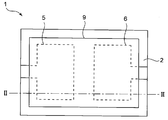
- FIG. 1 represents a plan view of an active device of the present invention.
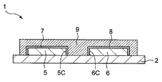
- FIG. 2 is a sectional view of the active element shown in FIG. 1 taken along the line II-II.
- FIG. 4 represents a cross-sectional view of another example of the active device of the present invention. The top view of the further another example of the active element of this invention is represented.
- FIG. 5 is a VV sectional view of the active element shown in FIG. 4.
- FIG. 6 represents a cross-sectional view of still another example of the active device of the present invention.
- the modification of sectional drawing of the active element of this invention is represented.
- the modification of sectional drawing of the active element of this invention is represented.
- the modification of sectional drawing of the active element of this invention is represented.
- the modification of sectional drawing of the active element of this invention is represented.
- an active element is an element that performs signal amplification and rectification, and is, for example, an element such as a transistor, a thyristor, or a diode. Examples of these applications include displays, touch panels, solar cells, semiconductor lasers, pressure sensors, and biosensors.
- the active element has a thickness direction and a surface direction.
- the thickness direction of the active element is a direction in which the base material, the first electrode, the second electrode, and the organic semiconductor layer are laminated, and the surface direction of the active element is a direction orthogonal to the thickness direction.
- FIG. 1 shows a plan view of the active element of the present invention
- FIG. 2 shows a II-II cross-sectional view of the active element shown in FIG.
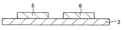
- the active element 1 of the present invention includes a substrate 2, a first electrode 5 and a second electrode 6, surface films 7 and 8, and an organic semiconductor layer 9.
- the base material 2 has one main surface and the other main surface, and is provided to support the first electrode 5, the second electrode 6, and the organic semiconductor layer 9.
- a flexible substrate made of a polymer film such as polyethylene naphthalate (PEN), polyethylene terephthalate (PET), polyimide (PI), or a rigid substrate such as a glass substrate is preferably used.
- PEN polyethylene naphthalate
- PET polyethylene terephthalate
- PI polyimide
- a rigid substrate such as a glass substrate
- the thickness of the base material 2 is preferably, for example, 5 ⁇ m or more, more preferably 10 ⁇ m or more, and further preferably 18 ⁇ m or more.
- the thickness of the substrate 2 is preferably 200 ⁇ m or less, more preferably 150 ⁇ m or less, and further preferably 125 ⁇ m or less.
- the thickness of the substrate 2 is preferably 10 ⁇ m or less, more preferably 7 ⁇ m or less, and further preferably 5 ⁇ m or less. Preferably, it is 0.1 ⁇ m or more, more preferably 0.5 ⁇ m or more, and further preferably 1 ⁇ m or more.
- the active element 1 of the present invention has a first electrode 5 and a second electrode 6 that are formed adjacent to each other on one main surface of a substrate 2.
- the first electrode 5, the second electrode 6, and a third electrode 11 described later are electrically connected to operate the active element 1, for example,
- the active element 1 is a transistor
- the first electrode 5 corresponds to a source electrode
- the second electrode 6 corresponds to a drain electrode
- the third electrode 11 corresponds to a gate electrode.
- the electrode material for example, conductive materials such as Cu, Al, Ag, C, Ni, Au, ITO, ZnO, IGO, IGZO, carbon nanotubes, graphene, and graphite can be used.
- conductive materials such as Cu, Al, Ag, C, Ni, Au, ITO, ZnO, IGO, IGZO, carbon nanotubes, graphene, and graphite can be used.
- Cu having high conductivity and being obtained at low cost is suitable for industrial production.
- the electrode can be formed by, for example, a photolithography method or a printing method. From the viewpoint of improving the accuracy of the relative positions of the first electrode 5 and the second electrode 6, the first electrode 5 and the second electrode 6 are preferably formed by a photolithography method.
- the thickness of the electrode is, for example, preferably 5 nm or more, more preferably 10 nm or more, and further preferably 20 nm or more in order to ensure the necessary electrical conductivity.
- the upper limit of the thickness of the electrode is not particularly limited, but is preferably 1 ⁇ m or less, for example, from the viewpoint of suppressing an increase in the entire thickness of the active element 1 and shortening the etching time when using a photolithography method, It is more preferably 700 nm or less, and further preferably 500 nm or less.
- the first electrode and the second electrode need only be formed adjacent to each other, and one side of the first electrode and one side of the second electrode may be arranged to face each other.
- the one side 5C of the first electrode 5 and the one side 6C of the second electrode are arranged to face each other.
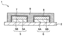
- FIG. 3 shows a sectional view of another example of the active element of the present invention.
- the 1st electrode 5 or the 2nd electrode 6 may be laminated
- the first electrode 5 includes a lower first electrode 5A formed on one main surface of the substrate 2 and an upper first electrode 5B formed on the lower first electrode 5A. You may have.
- the second electrode 6 includes a lower second electrode 6A formed on one main surface of the substrate 2 and an upper second electrode formed on the lower second electrode 6A. You may have the electrode 6B.
- the performance of the active element 1 can be enhanced by appropriately selecting the electrode material disposed on the lower side and the electrode material disposed on the upper side.
- the distance between the first electrode 5 and the second electrode 6 is not particularly limited.
- the first electrode 5 and the second electrode 6 is a drain electrode
- the channel length, which is a length between 6, is preferably 20 ⁇ m or less, more preferably 15 ⁇ m or less, and even more preferably 10 ⁇ m or less. The shorter the channel length, the higher the transistor processing speed and integration.
- the surface films 7 and 8 are formed on the first electrode 5 and the second electrode 6. Since it has the effect of making the wet spread of the organic semiconductor ink uniform, variation in the performance of the active element 1 can be suppressed. Further, the surface films 7 and 8 also have an effect of lowering an energy barrier between the electrode and the organic semiconductor.
- the first electrode 5 and the second electrode 6 are the upper side of the first electrode 5 and the upper side of the second electrode 6 in the thickness direction.
- the peak of the FT-IR spectrum after contacting 45 seconds in the developer pH 10 ⁇ 12 is, (A) 1000 cm -1 and more 1300 cm -1 or less, (B) 1715 cm -1 or 1750cm -1 or less exists in each range.
- the details of the mechanism are not necessarily clear, but if the surface films 7 and 8 have a peak of the FT-IR spectrum in the above wave number range, the organic semiconductor ink tends to spread uniformly on the surface films 7 and 8. Therefore, variation in the performance of the active element 1 can be suppressed. Moreover, the energy barrier between an organic semiconductor and an electrode can be reduced.
- the fact that the peak of the FT-IR spectrum exists in the above wave number range means that the material of the surface films 7 and 8 is a resin having an ester group.
- a process of providing a monomolecular film or a bank is required separately from the process of forming the electrode.
- a photosensitive resin composition such as a dry film resist or a liquid resist used for forming the partition wall (including a curing agent, a solvent, etc. in addition to the photosensitive resin.
- photosensitive resin simply referred to as “photosensitive resin”.
- the surface films 7 and 8 can be used. For this reason, it becomes possible to form the surface films 7 and 8 in the step of forming the partition walls, and the step of separately providing a monomolecular film or a bank can be omitted.
- Examples of the material for the surface films 7 and 8 include aliphatic esters, formate esters, aromatic esters, and lactones. Specific examples include acrylic resins, methacrylic resins, urethane resins, vinyl ester resins, alkyd resins, epoxy ester resins, polyester resins, allyl resins, or combinations thereof.
- the surface membrane 7 and 8 pH 10 FT-IR spectrum peak of after developing solution is contacted 45 seconds to 12, (A) and 1000 cm -1 or 1300 cm -1 or less, (B1) 1735cm -1 or 1750cm It is preferable that at least one each exists in the range of ⁇ 1 or less. If the surface films 7 and 8 have a peak of the FT-IR spectrum in the wave number range, the energy barrier between the organic semiconductor and the electrode can be further reduced. In general, since the aliphatic ester has a peak in the above wavenumber range, the surface film preferably contains the aliphatic ester.
- the surface films 7 and 8 preferably have an anticorrosive effect for the electrodes.
- a rust preventive agent may be added to the surface films 7 and 8.
- a material that is already used as a rust preventive agent is used.
- imidazole, triazole, benzotriazole, benzimidazole, benzthiazole, pyrazole and the like may be used.
- monocyclic or polycyclic azoles such as halogen, alkyl, and phenyl-substituted products, aromatic amines such as aniline, aliphatic amines such as alkylamine, salts thereof, and the like. There is no need to be limited to the materials described herein.
- the surface films 7 and 8 may contain a curing agent such as an epoxy-based, urethane-based, acrylic-based thermosetting resin, urethane acrylate-based, cyanoacrylate-based ultraviolet curable resin, or the like.
- a curing agent such as an epoxy-based, urethane-based, acrylic-based thermosetting resin, urethane acrylate-based, cyanoacrylate-based ultraviolet curable resin, or the like.
- the surface films 7 and 8 can be formed by using a general-purpose printing method such as gravure, screen and offset, as well as various coater methods, coating and dipping methods, and various methods such as a dry film resist method, followed by exposure. ⁇ Develop and pattern.
- the surface films 7 and 8 are preferably formed by a dry film resist method.
- the thickness of the surface films 7 and 8 is preferably 1 nm or more, more preferably 3 nm or more, and further preferably 5 nm or more. If the thickness of the surface films 7 and 8 is less than 1 nm, the organic semiconductor ink may be spread unevenly.
- the thickness of the surface films 7 and 8 is preferably 40 nm or less, more preferably 30 nm or less, and further preferably 20 nm or less. If the thickness of the surface films 7 and 8 exceeds 40 nm, the energy barrier between the organic semiconductor and the electrode may increase.
- the surface films 7 and 8 are also formed on the opposing surfaces of the first electrode 5 and the second electrode 6, respectively.
- the active element 1 is a transistor in which the first electrode 5 and the second electrode 6 function as a source electrode and a drain electrode, respectively, improvement of the wettability between the organic semiconductor and the electrode in the vicinity of the channel region, Contributes to decline.
- the surface films 7 and 8 may be formed on the entire surfaces of the first electrode 5 and the second electrode 6, respectively. This is preferable because the area where the energy barrier between the organic semiconductor and the electrode is lowered can be widened.
- the thickness of the surface film 7 formed on the first electrode 5 and the thickness of the surface film 8 formed on the second electrode 6 may be the same or different. Further, the surface films 7 and 8 may partially differ in thickness or may be constant throughout.
- the surface films 7 and 8 may be a single layer, or a plurality of layers may be laminated.
- the wettability of the surface films 7 and 8 is greater than the wettability of the first electrode 5 and the second electrode 6.
- the wettability of the surface film means the wettability of the organic semiconductor ink for forming the organic semiconductor layer with respect to the surface film. The higher the wettability of the surface film, the easier the organic semiconductor ink on the surface film spreads in the surface direction.
- the wettability of the electrode means the wettability of the organic semiconductor ink forming the organic semiconductor layer with respect to the electrode.
- the wettability can be evaluated by the following index.
- the contact angle is an angle formed by a liquid surface and a solid surface, and is measured based on a wettability test method for the surface of a JIS R 3257: 1999 substrate glass. Although it is desirable that the contact angle of the liquid organic semiconductor ink is directly measured, in order to more easily evaluate the wettability, it is assumed that the contact angle of the organic semiconductor ink is proportional to the contact angle of water. The contact angle may be measured.
- the contact angle between the surface film and the organic semiconductor ink is preferably 30 degrees or less, more preferably 20 degrees or less, and even more preferably 10 degrees or less. .
- the surface free energy can be obtained from the following extended Fowkes equation (1) and Young equation (2) using the values of the contact angle and the surface tension of the measurement liquid.
- the contact angle measurement solution can be selected from pure water, liquid paraffin, glycerin, methylene iodide, n-hexadecane, ⁇ -bromonaphthalene, and the like.
- the surface free energy of the surface film is large, the adhesion force of the organic semiconductor ink to the surface film is increased, so that the organic semiconductor ink is likely to wet and spread in the surface direction on the surface film. Therefore, the surface free energy of the surface film is preferably larger than that of the electrode.
- FIG. 4 shows a plan view of still another example of the active element of the present invention
- FIG. 5 shows a VV cross-sectional view of the active element shown in FIG.
- a partition wall 13 formed on one main surface of the substrate 2 and on the outer side in the plane direction than the organic semiconductor layer 9 may be provided.
- the partition wall 13 is formed on one main surface of the substrate 2, on the outer side in the surface direction than the organic semiconductor layer 9, and in a region different from the region where the first electrode 5 and the second electrode 6 are formed. Also good.
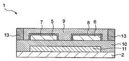
- FIG. 6 shows a cross-sectional view of yet another example of the active device of the present invention.
- the partition wall 13 is formed on the first electrode 5 or the second electrode 6 as long as it is on one main surface of the substrate 2 and outside the organic semiconductor layer 9 in the surface direction. It may be.
- An insulating material is used for the partition wall 13 formed on the electrode. For example, after forming a resist on one main surface of the substrate 2, the first electrode, and the second electrode, the portion where the partition wall is to be formed is exposed, and the portion where the surface film is formed on the electrode is unexposed. . When the developing solution is brought into contact with the resist, the exposed portion of the resist becomes the partition wall 13, and a part of the resist remains on the first electrode 5 and the second electrode 6 as the surface films 7 and 8 in the unexposed portion.
- the position where the partition wall 13 is formed is not particularly limited, but when the partition wall 13 is formed of a conductive material, it is necessary to insulate from the first electrode 5 and the second electrode 6. Therefore, when the partition wall 13 is made of a conductive material, the partition wall 13 is preferably not in contact with the first electrode 5 and the second electrode 6 as shown in FIGS. That is, the partition wall 13 is preferably arranged outside the first electrode 5 and the second electrode 6 in the surface direction of the substrate 2.
- the partition wall 13 is preferably arranged so as to surround the organic semiconductor layer 9 as much as possible. Thereby, wetting of the organic semiconductor ink can be reliably stopped.
- a square-shaped partition wall 13 surrounding the entire circumference of the organic semiconductor layer 9 is shown.
- the two strip-shaped partition walls 13 are provided in parallel above and below the channel region formed by the first electrode 5 and the second electrode 6 in a plan view. May be.
- At least one partition wall 13 is provided, and a plurality of partition walls 13 may be provided.
- a plurality of partition walls 13 may be formed.
- the arrangement relationship between one partition wall and another partition wall is not limited.
- the one partition wall and the other partition wall can be disposed to face each other.
- the partition wall 13 may be formed of a conductive material such as Cu, Al, Ag, C, Ni, Au, ITO, ZnO, IGO, IGZO, carbon nanotube, graphene, and graphite, like the electrode. , 8 may be used. From the viewpoint of reducing the number of processes, the partition wall 13 is preferably formed of the same material as that of the surface films 7 and 8 as described later in “2. Active device manufacturing method”.
- the partition wall 13 is formed to be higher than the height of the surface films 7 and 8 on the first electrode 5 and the second electrode 6. It is preferable that the film is formed higher than the surface films 7 and 8 on the first electrode 5 and the second electrode 6.
- the organic semiconductor ink spreads on the surface films 7 and 8 but is blocked by the partition wall 13. Therefore, the wettability of the surface films 7 and 8 is preferably larger than the wettability of the partition wall 13.
- the active element 1 of the present invention includes an insulating layer 10 formed on the organic semiconductor layer 9 and a third electrode 11 formed on the insulating layer 10. Also good.
- the first electrode 5 is a source electrode
- the second electrode 6 is a drain electrode
- the third electrode 11 is a gate electrode
- a top-gate transistor in which the gate electrode is disposed on the upper side with respect to the source electrode and the drain electrode is configured. be able to.
- the active element 1 of the present invention includes a third electrode 11 formed on one main surface of the base 2 and an insulating layer 10 formed on the third electrode 11. You may have.
- the first electrode 5 and the second electrode 6 are formed on the insulating layer 10.
- the gate electrode is disposed on the lower side (side closer to the substrate 2) with respect to the source electrode and the drain electrode.
- a bottom-gate transistor can be formed.
- the insulating layer 10 functions as a gate insulating film.
- the insulating layer 10 is preferably formed from an insulating material such as SiO 2 or SiON.
- the thickness of the insulating layer 10 is preferably 200 nm or more, more preferably 250 nm or more, and further preferably 300 nm or more.
- the thickness of the insulating layer 10 is preferably 600 nm or less, more preferably 550 nm or less, and further preferably 500 nm or less.
- the active element 1 of the present invention may have a third electrode 11 formed on the other main surface of the substrate 2.
- the first electrode 5 is a source electrode
- the second electrode 6 is a drain electrode
- the third electrode 11 is a gate electrode
- a transistor in which the base material 2 also serves as a gate insulating film can be configured.
- the organic semiconductor layer 9 is formed on one main surface of the substrate 2 so as to cover at least a region between the first electrode 5 and the second electrode 6.
- the organic semiconductor layer 9 functions as a channel region when the active element 1 is a transistor.
- a material of the organic semiconductor layer 9 for example, pentacene, anthracene, tetracene, rubrene, polyacetylene, polythiophene, fullerene, carbon nanotube, or the like can be used.
- the upper limit of the thickness of the organic semiconductor layer 9 is not particularly limited, but in order to obtain a thin active element 1, the thickness of the organic semiconductor layer 9 is preferably 200 nm or less, and more preferably 150 nm or less, for example. Preferably, it is 100 nm or less.
- the organic semiconductor layer 9 is preferably formed by a printing method. More specifically, it is formed by applying a liquid mixture (hereinafter referred to as “organic semiconductor ink”) in which organic semiconductor molecules are dispersed in an organic solvent for application to the substrate 2 and then drying.
- organic semiconductor ink a liquid mixture
- organic semiconductor ink in which organic semiconductor molecules are dispersed in an organic solvent for application to the substrate 2 and then drying.
- the organic semiconductor layer 9 is formed by a printing method, for example, mesitylene, toluene, chloroform, p-diisopropylbenzene, benzyl alcohol, or a mixed solvent thereof can be used as the organic solvent.
- FIGS. 10 to 20 are process sectional views showing a method for manufacturing an active device of the present invention.
- the active element manufacturing method of the present invention includes (1) a step of forming a first electrode and a second electrode adjacent to each other on one main surface of a substrate, and (2) a first electrode on one main surface of the substrate. And a step of forming a resist layer on one main surface of the second electrode, and (3) a region between the first electrode and the second electrode on the one main surface of the substrate by bringing the resist layer into contact with a developer.
- the base material 2 is prepared.
- an adhesion layer, a planarization layer, an optical adjustment layer, and the like may be formed on the main surface of the substrate 2.
- puncturing with a needle-like object, punching, laser processing or the like can be used.
- the first conductive layer 3 is formed on one main surface of the substrate 2.
- the first conductive layer 3 is for forming various electrodes such as a source electrode, a drain electrode, a gate electrode, a terminal electrode, and a via electrode.
- the method for forming the first conductive layer 3 is not particularly limited, and for example, a vacuum deposition method or a sputtering method can be used. Moreover, when the through-hole which penetrates in the thickness direction is not formed in the base material 2, the 1st conductive layer 3 can also be formed into a film by sticking the conductive material formed in foil shape. Although not shown, a second conductive layer may be further formed on the first conductive layer 3. Thereby, since an electrode can be made into a laminated structure, since an electrode material and a shape can be designed independently on the upper side and the lower side, it is possible to achieve both good operating characteristics and the possibility of selecting an inexpensive material.
- Examples of the material of the first conductive layer 3 and the second conductive layer include conductive materials such as Cu, Al, Ag, C, Ni, Au, ITO, ZnO, IGO, IGZO, carbon nanotubes, graphene, and graphite. Can be used
- a mask layer is formed on the first conductive layer.
- a specific method for forming the mask layer is as follows. As shown in FIG. 12, a photosensitive resin composition such as a dry film resist or a liquid resist (including a curing agent, a solvent, etc. in addition to the photosensitive resin. (Resist) ") 20 is applied.
- the photosensitive resin includes a negative type in which the exposed portion is insoluble in the developer and a positive type in which the exposed portion is soluble in the developer.
- a negative photosensitive resin is taken as an example. explain.
- a resist is applied on the first conductive layer, and an electron beam or light (ultraviolet rays) is irradiated on the resist to draw a predetermined circuit shape on the resist.
- the shape of the first electrode and the second electrode (for example, a source electrode and a drain electrode in the case of a transistor) is drawn on the resist.
- the circuit shape is transferred and baked on the resist.
- the unexposed portion of each resist is dissolved in the developer.
- the resist exposed portions remain on the first conductive layer 3 as mask layers 20a and 20b.
- the mask layer can be formed of a dry film resist or a liquid resist, but is preferably formed of a dry film resist. Compared with the case where the mask layer is formed of a liquid resist, the solvent drying after applying the resist is unnecessary, so that productivity is improved.
- the first conductive layer 3 is brought into contact with the etching solution. By this operation, as shown in FIG. 14, the region of the first conductive layer 3 that is not covered with the mask layer is removed.
- the mask layers 20a and 20b covering the first electrode 5 and the second electrode 6 are peeled off by bringing the mask layers 20a and 20b formed on the first electrode 5 and the second electrode 6 into contact with a stripping solution and dissolving them. .
- the first electrode 5 and the second electrode 6 that are adjacent to each other on one main surface of the substrate 2 are formed.
- a resist layer 12 is formed on one main surface of the substrate 2 and on one main surface of the first electrode 5 and the second electrode 6.
- the resist layer 12 can be formed by applying a photosensitive resin such as a dry film resist or a liquid resist in the same manner as the mask layers 20a and 20b.
- the circuit shape is transferred and baked on the resist layer 12.
- the surface films 7 and 8 also have the effect that the energy barrier between an organic semiconductor and an electrode can be reduced.
- the present invention is suitable for industrial production because such surface films 7 and 8 can be formed by a simple method of removing a part of the resist layer 12 formed on the electrodes.
- the organic semiconductor layer 9 is formed on one main surface of the substrate 2 so as to cover at least a region between the first electrode 5 and the second electrode 6. Thereby, the active element 1 in which the organic semiconductor layer 9 is formed on one main surface of the substrate 2 from which the first conductive layer 3 is removed can be manufactured.
- a partition wall 13 may be formed to prevent the organic semiconductor layer 9 from becoming too wet and spread on the substrate 2 as shown below. That is, after (2) the resist layer forming step, (3) before the step of contacting the resist layer with the developer (surface film forming step), (5) between the first electrode 5 and the second electrode 6. The resist layer 12 outside the region is exposed. Then, (3) the partition wall 13 may be formed outside the region between the first electrode 5 and the second electrode 6 on the one main surface of the substrate 2 by contacting the resist layer 12 with the developer. . Thereby, the exposed part of the resist layer 12 becomes the partition wall 13, and the unexposed part becomes the surface films 7 and 8 formed on the electrodes. By performing the step (5), the partition wall 13 and the surface films 7 and 8 can be formed together in the step (3), and the step of providing the partition wall 13 can be omitted.
- next step (6) can be performed after the step (4).
- Step of forming an insulating layer on the organic semiconductor layer and forming a third electrode on the insulating layer As shown in FIG. 19, the insulating layer 10 is formed on the organic semiconductor layer 9. Next, as shown in FIG. 20, the third electrode 11 is formed on the insulating layer 10.
- a top gate type transistor in which the first electrode 5, the second electrode 6, and the third electrode 11 correspond to the source electrode, the drain electrode, and the gate electrode, respectively, is manufactured. Can do.
- step (7) can be performed before the step (1).
- Step of forming a third electrode on one main surface of the base material and forming an insulating layer on the third electrode Preparation of the base material 2, and provision of the third electrode 11 on the one main surface of the base material 2 Form.
- the third electrode 11 can be formed by a printing method or a photolithography method. When the photolithography method is used, a mask layer having a desired shape is formed on the third conductive layer after forming a third conductive layer (not shown) in the same manner as the formation of the first electrode 5 and the second electrode 6. Then, the third electrode 11 is formed by bringing the third conductive layer into contact with the etching solution. Next, the insulating layer 10 is formed on the third electrode 11.
- a bottom-gate transistor in which the first electrode 5, the second electrode 6, and the third electrode 11 correspond to the source electrode, the drain electrode, and the gate electrode, respectively. can be manufactured.
- sample A7 was immersed in a SAM treatment solution (10 mM, pentafluorobenzenethiol, solvent: isopropyl alcohol) for 5 minutes for SAM treatment to form a self-assembled monolayer on the electrode.
- TFT characteristics (3-1) Preparation of sample Example 5: A conductive layer made of Cu is formed on one main surface of a PEN substrate, a pattern resist is laminated, and exposure, development, etching, peeling, A source electrode, a drain electrode, and other wirings are formed. Lamination, exposure, and development of the same rust-preventing resist used for work function and FT-IR spectrum measurement, surface films are formed on the source and drain electrodes, and barrier ribs are formed to surround the channel portion did. Subsequently, organic semiconductor ink was apply
- Comparative Example 8 A conductive layer made of Cu was formed on one main surface of a PEN substrate, a pattern resist was laminated, exposed, developed, etched, and peeled to form a source electrode, a drain electrode, and other wirings. A partition made of a fluororesin was formed so as to surround the channel portion using a dispenser. Subsequently, organic semiconductor ink was apply
- Comparative Example 9 A conductive layer made of Cu is formed on one main surface of a PEN substrate, a pattern resist is laminated, exposed, developed, etched, and peeled to form a source electrode, a drain electrode, and other wirings.
- a partition made of a fluororesin was formed so as to surround the channel portion using a dispenser.
- the source electrode and the drain electrode were immersed in a SAM treatment solution (10 mM, pentafluorobenzenethiol, solvent: isopropyl alcohol) for 5 minutes to form self-assembled monolayers on the source electrode and the drain electrode. Subsequently, organic semiconductor ink was apply
- the gate voltage-drain current characteristic was measured with a 4200-SCS type semiconductor parameter analyzer manufactured by KEITHLEY.
- the measurement conditions of the transfer characteristics were a drain voltage of ⁇ 20V and a gate voltage scanning range of 10V to ⁇ 20V.
- the mobility was calculated from the obtained transfer characteristics.
- Table 3 shows the results of measuring the maximum drain current (A), mobility (cm 2 / V ⁇ sec), and On / Off ratio.
- the maximum drain current of the sample C1 according to Example 5 was almost the same as that of the sample C3 according to Comparative Example 9. Further, since the mobility of Example 5 exceeded the results of Comparative Examples 8 to 9, it can be expected that the sample C1 according to Example 5 operates as an element having a high switching speed. On the other hand, it was found that there was room for improvement in the On / Off ratio of Sample C1.
- a resist containing a rust inhibitor is used as a surface film, a work function comparable to that obtained when the SAM treatment is performed can be obtained. Further, it was found that such a surface film is considered to contain an ester from the position of the peak of the FT-IR spectrum. Furthermore, an active element having an electrode on which such a surface film is formed has a high maximum drain current and mobility.
- active element 2 substrate 3: first conductive layer 5: first electrode 6: second electrode 7, 8: surface film 9: organic semiconductor layer 10: insulating layer 11: third electrode 12: resist layer 13: Partition 20: Resist 20a, 20b: Mask layer
Landscapes
- Thin Film Transistor (AREA)
- Electroluminescent Light Sources (AREA)
- Electrodes Of Semiconductors (AREA)
Abstract
【課題】 本発明は、有機半導体と電極の間のエネルギー障壁が低い能動素子とその製造方法を提供することを目的とする。 【解決手段】 本発明の能動素子1は、基材2と、基材2の一方主面上に隣り合って形成されている第1電極5および第2電極6と、第1電極5上および第2電極6上に形成されている表面膜7、8と、基材2の一方主面上であって、少なくとも第1電極5と第2電極6の間の領域を覆うように形成されている有機半導体層9と、を有し、表面膜7、8は、pH10~12の現像液に45秒接触させた後のFT-IRスペクトルのピークが、(A)1000cm-1以上1300cm-1以下と、(B)1715cm-1以上1750cm-1以下の範囲にそれぞれ少なくとも一つ存在している。
Description
本発明は、半導体層に有機半導体を用いた能動素子に関するものである。
近年、能動素子の薄型化、フレキシブル化、軽量化、大面積化等の要望が高まるにつれて、基材材料としてはポリエチレンナフタレート(PEN)やポリイミド(PI)等の高分子フィルムが使用されている。これに伴い、半導体層として、当該フィルムの耐熱温度以下で成膜が可能な有機半導体を用いた能動素子が種々開発されている。有機半導体との間のエネルギー障壁を小さくすることにより、高いキャリア注入効率が得られる。 電極と有機半導体との間のエネルギー障壁を低くするために、例えば、自己組織化単分子膜処理を施し、電極と有機半導体の間に単分子膜を設けたり(非特許文献1)、有機半導体を含有するインキのぬれ広がりを抑制するためのバンク(隔壁)が形成される(特許文献1)。
岩佐義宏、竹延大志、"有機トランジスタ"、[online]、2008年、応用物理学会、[2016年6月15日検索]、インターネット<URL:http://www.jsap.or.jp/editorial/KISO-sample/QOBU0414.pdf>
しかし、従来の方法では自己組織化単分子膜やバンクを形成するための工程数が増加することになる。特にバンクを設ける場合にはマージンを考慮して設計する必要がある。より簡便な方法で、電極上に有機半導体インキを均一に広げて素子としての性能のバラツキを抑えるとともに、有機半導体-電極間のエネルギー障壁を低くすることができる能動素子やその製造方法が求められている。
そこで、本発明は、有機半導体と電極の間のエネルギー障壁が低い能動素子とその製造方法を提供することを目的とする。
そこで、本発明は、有機半導体と電極の間のエネルギー障壁が低い能動素子とその製造方法を提供することを目的とする。
上記目的を達成し得た本発明の能動素子は、基材と、該基材の一方主面上に隣り合って形成されている第1電極および第2電極と、第1電極上および第2電極上に形成されている表面膜と、基材の一方主面上であって、少なくとも第1電極と第2電極の間の領域を覆うように形成されている有機半導体層と、を有し、表面膜は、pH10~12の現像液に45秒接触させた後のFT-IRスペクトルのピークが、(A)1000cm-1以上1300cm-1以下と、(B)1715cm-1以上1750cm-1以下の範囲にそれぞれ少なくとも一つ存在している点に要旨を有する。メカニズムの詳細については必ずしも明らかではないが、表面膜が上記波数範囲にFT-IRスペクトルのピークを有していれば、表面膜上で有機半導体インキが均一にぬれ広がりやすくなるため、能動素子の性能のバラツキを抑制できる。また、有機半導体と電極との間のエネルギー障壁を低下することができる。なお、FT-IRスペクトルのピークが上記の波数範囲に存在しているとは、表面膜の材料がエステル基を有する樹脂であることを意味している。
表面膜は、pH10~12の現像液に45秒接触させた後のFT-IRスペクトルのピークが、(A)1000cm-1以上1300cm-1以下と、(B1)1735cm-1以上1750cm-1以下の範囲にそれぞれ少なくとも一つ存在していることが好ましい。表面膜が上記波数範囲にFT-IRスペクトルのピークを有していれば、有機半導体と電極との間のエネルギー障壁の低下をより一層高められる。
表面膜の厚みが1nm以上40nm以下であることが好ましい。表面膜の厚みが1nm未満であると、有機半導体インキが不均一にぬれ広がるおそれがある。表面膜の厚みが40nmを超えると、有機半導体と電極との間のエネルギー障壁が増大するおそれがある。
表面膜は、第1電極および第2電極の向かい合う面上にもそれぞれ形成されていることが好ましい。能動素子が、第1電極と第2電極がそれぞれソース電極およびドレイン電極として機能するトランジスタである場合に、チャネル領域付近での有機半導体と電極とのぬれ性の改善や、エネルギー障壁の低下に寄与する。
第1電極および第2電極の材料がCuであることが好ましい。導電率が高く安価に得られるCuが工業生産上適している。
基材の一方主面上であって、有機半導体層よりも面方向外側に形成されている隔壁を有することが好ましい。基材上で有機半導体インキがぬれ広がり過ぎることを制御できる。
また、上記目的を達成し得た本発明の能動素子の製造方法は;基材の一方主面上に隣り合う第1電極および第2電極を形成する工程と;基材の一方主面上、第1電極および第2電極の一方主面上にレジスト層を形成する工程と;レジスト層を現像液に接触させて、基材の一方主面上の第1電極と第2電極の間の領域のレジスト層と、第1電極および第2電極上のレジスト層の一部を除去することにより、第1電極上および第2電極上に表面膜を形成する工程と;基材の一方主面上であって、少なくとも第1電極と第2電極の間の領域を覆うように有機半導体層を形成する工程と;を含む点に要旨を有する。本発明の能動素子の製造方法は、性能のバラツキを抑制し、有機半導体と電極との間のエネルギー障壁を低下する効果を有する電極上の表面膜を、電極上に形成されたレジスト層の一部を除去するという簡便な方法で形成できるため、工業生産上適している。
本発明の能動素子の製造方法は、レジスト層を形成する工程の後、レジスト層を現像液に接触させる工程の前に、第1電極および第2電極の間の領域の外側のレジスト層を露光する工程を含み、レジスト層を現像液に接触させる工程により、基材の一方主面上の第1電極および第2電極の間の領域の外側に隔壁を形成することが好ましい。これにより、レジスト層のうち露光された部分が隔壁となり、未露光の部分は電極上に形成される表面膜となる。第1電極および第2電極の間の領域の外側のレジスト層を露光する工程を行うことにより、レジスト層を現像液に接触させる工程において隔壁と表面膜を一緒に形成することが可能となり、別途隔壁を設ける工程を省略することができる。
本発明の能動素子は、表面膜上で有機半導体インキが均一にぬれ広がりやすくなるため、能動素子の性能のバラツキを抑制できる。また、有機半導体と電極との間のエネルギー障壁を低下することができる。
また、本発明の能動素子の製造方法は、性能のバラツキを抑制し、有機半導体と電極との間のエネルギー障壁を低下する効果を有する電極上の表面膜を、電極上に形成されたレジスト層の一部を除去するという簡便な方法で形成できるため、工業生産上適している。
また、本発明の能動素子の製造方法は、性能のバラツキを抑制し、有機半導体と電極との間のエネルギー障壁を低下する効果を有する電極上の表面膜を、電極上に形成されたレジスト層の一部を除去するという簡便な方法で形成できるため、工業生産上適している。
以下、本発明に関して、図面を参照しつつ具体的に説明するが、本発明はもとより図示例に限定される訳ではなく、前、後記の趣旨に適合し得る範囲で適当に変更を加えて実施することも可能であり、それらはいずれも本発明の技術的範囲に包含される。
1.能動素子
本発明において能動素子は、信号増幅や整流を行う素子であり、例えばトランジスタ、サイリスタ、ダイオード等の素子である。これらの応用例としては、例えば、ディスプレイ、タッチパネル、太陽電池、半導体レーザ、圧力センサー、生体センサー等がある。
本発明において能動素子は、信号増幅や整流を行う素子であり、例えばトランジスタ、サイリスタ、ダイオード等の素子である。これらの応用例としては、例えば、ディスプレイ、タッチパネル、太陽電池、半導体レーザ、圧力センサー、生体センサー等がある。
本発明において能動素子は、厚み方向と面方向を有する。能動素子の厚み方向は、基材、第1電極、第2電極、有機半導体層が積層される方向であり、能動素子の面方向は、厚み方向と直交する方向である。
図1は、本発明の能動素子の平面図を表し、図2は、図1に示した能動素子のII-II断面図を表す。図1~図2に示すように、本発明の能動素子1は、基材2と、第1電極5および第2電極6と、表面膜7、8と、有機半導体層9と、を有する。
基材2は、一方主面と他方主面を有しており、第1電極5、第2電極6、有機半導体層9を支持するために設けられる。
基材2は、例えば、ポリエチレンナフタレート(PEN)、ポリエチレンテレフタレート(PET)、ポリイミド(PI)等の高分子フィルムからなるフレキシブル基板や、ガラス基板等のリジッド基板が好ましく用いられる。
基材2の折れや破れを防止するために、基材2の厚みは、例えば5μm以上であることが好ましく、10μm以上であることがより好ましく、18μm以上であることがさらに好ましい。他方、能動素子1の薄型化の観点からは、基材2の厚みは、200μm以下であることが好ましく、150μm以下であることがより好ましく、125μm以下であることがさらに好ましい。
後述するように、基材2が絶縁層を兼ねるフィルムの場合には、基材2の厚みは、10μm以下であることが好ましく、7μm以下であることがより好ましく、5μm以下であることがさらに好ましく、0.1μm以上であることが好ましく、0.5μm以上であることがより好ましく、1μm以上であることがさらに好ましい。
図1に示すように、本発明の能動素子1は、基材2の一方主面上に隣り合って形成されている第1電極5および第2電極6とを有する。
第1電極5、第2電極6、後述する第3電極11(以下、まとめて「電極」と称することがある)は能動素子1を動作させるために電気的に接続されるものであり、例えば、能動素子1がトランジスタの場合には、第1電極5はソース電極に相当し、第2電極6はドレイン電極に相当し、第3電極11はゲート電極に相当する。
電極の材料は、例えば、Cu、Al、Ag、C、Ni、Au、ITO、ZnO、IGO、IGZO、カーボンナノチューブ、グラフェン、グラファイト等の導電性材料を用いることができる。特に、導電率が高く安価に得られるCuが工業生産上適している。
電極は、例えば、フォトリソグラフィ法や印刷法によって形成することができる。第1電極5と第2電極6の相対位置の精度を向上させる観点からは、第1電極5および第2電極6は、フォトリソグラフィ法によって形成されることが好ましい。
電極の厚みは、必要な導電率を確保するために、例えば、5nm以上であることが好ましく、10nm以上であることがより好ましく、20nm以上であることがさらに好ましい。電極の厚みの上限は特に制限されないが、能動素子1全体の厚みが増大するのを抑制し、フォトリソグラフィ法を用いる場合にエッチング時間を短縮する観点から、例えば、1μm以下であることが好ましく、700nm以下であることがより好ましく、500nm以下であることがさらに好ましい。
第1電極と第2電極は隣り合って形成されていればよく、第1電極の一つの辺と第2電極の一つの辺が対向して配置されていてもよい。例えば、図2では、第1電極5の一辺5Cと、第2電極の一辺6Cが対向するように配置されている。
図3は、本発明の能動素子の他の例の断面図を表す。図3に示すように、第1電極5または第2電極6は積層されていてもよい。詳細には、第1電極5は、基材2の一方主面上に形成されている下側第1電極5Aと、下側第1電極5A上に形成されている上側第1電極5Bとを有していてもよい。第1電極5と同様に、第2電極6は、基材2の一方主面上に形成されている下側第2電極6Aと、下側第2電極6A上に形成されている上側第2電極6Bとを有してもよい。下側に配置される電極材料と、上側に配置される電極材料を適切に選択することにより能動素子1の性能を高められる。
第1電極5と第2電極6の間隔は特に制限されないが、例えば第1電極5がソース電極で、第2電極6がドレイン電極であるトランジスタの場合には、第1電極5と第2電極6の間の長さであるチャネル長は20μm以下であることが好ましく、15μm以下であることがより好ましく、10μm以下であることがさらに好ましい。チャネル長が短いほど、トランジスタの処理速度と集積度を高めることができる。
表面膜7、8は、第1電極5上および第2電極6上に形成されるものである。有機半導体インキのぬれ広がりを均一にする効果を有するため、能動素子1の性能のバラツキを抑制できる。また、表面膜7、8は電極と有機半導体の間のエネルギー障壁を低下させる効果も有する。ここで、第1電極5上および第2電極6上とは、厚み方向における第1電極5の上側および第2電極6の上側である。
表面膜7、8は、pH10~12の現像液に45秒接触させた後のFT-IRスペクトルのピークが、(A)1000cm-1以上1300cm-1以下と、(B)1715cm-1以上1750cm-1以下の範囲にそれぞれ少なくとも一つ存在している。メカニズムの詳細については必ずしも明らかではないが、表面膜7、8が上記波数範囲にFT-IRスペクトルのピークを有していれば、表面膜7、8上で有機半導体インキが均一にぬれ広がりやすくなるため、能動素子1の性能のバラツキを抑制できる。また、有機半導体と電極との間のエネルギー障壁を低下することができる。なお、FT-IRスペクトルのピークが上記の波数範囲に存在しているとはつまり、表面膜7、8の材料がエステル基を有する樹脂であることを意味している。
従来、電極表面に自己組織化単分子膜を設けたり、基材上にバンクを設けるには、電極を形成する工程とは別に単分子膜やバンクを設ける工程が必要であった。これに対して、本発明では、隔壁の形成に用いられるドライフィルムレジストや液体レジスト等の感光性樹脂組成物(感光性樹脂以外に硬化剤、溶剤等を含む。以下、単に「感光性樹脂」ということがある)を表面膜7、8とすることができる。このため、隔壁の形成工程で表面膜7、8の形成が可能となり、別途単分子膜やバンクを設ける工程を省略することができる。
表面膜7、8の材料としては、脂肪族エステル、ギ酸エステル、芳香族エステル、ラクトン等が挙げられる。具体的には、例えば、アクリル樹脂、メタクリル樹脂、ウレタン樹脂、ビニルエステル樹脂、アルキド樹脂、エポキシエステル樹脂、ポリエステル樹脂、アリル樹脂またはこれらの組み合わせ等が挙げられる。
表面膜7、8は、pH10~12の現像液に45秒接触させた後のFT-IRスペクトルのピークが、(A)1000cm-1以上1300cm-1以下と、(B1)1735cm-1以上1750cm-1以下の範囲にそれぞれ少なくとも一つ存在していることが好ましい。表面膜7、8が上記波数範囲にFT-IRスペクトルのピークを有していれば、有機半導体と電極との間のエネルギー障壁の低下をより一層高められる。一般に、脂肪族エステルが上記波数範囲にピークを有するため、表面膜は脂肪族エステルを含むことが好ましい。
表面膜7、8は電極の防錆効果も有していることが好ましい。防錆機能を付与するために、表面膜7、8には防錆剤が添加されていてもよい。当該防錆剤としては、すでに防錆剤として公知に用いられる材料が使用され、具体例としては、例えばイミダゾール、トリアゾール、ベンゾトリアゾール、ベンズイミダゾール、ベンズチアゾール、ピラゾールなどを用いるとよい。また、これらのハロゲン、アルキル、フェニル置換体などの単環または多環式のアゾール類、アニリンなどの芳香族アミン類、アルキルアミンなどの脂肪族アミン、これらの塩などが挙げられ、また、特に本記載の材料に制限する必要はない。
表面膜7、8には、エポキシ系、ウレタン系、アクリル系などの熱硬化性樹脂や、ウレタンアクリレート系、シアノアクリレート系などの紫外線硬化型樹脂等の硬化剤が含まれていてもよい。
表面膜7、8の形成方法は、グラビア、スクリーン、オフセットなどの汎用の印刷法のほか、各種コーターによる方法、塗装、ディッピングなどの方法、ドライフィルムレジスト法などの各種方法により全面形成した後に露光・現像してパターニングするとよい。中でも、表面膜7、8はドライフィルムレジスト法により形成されることが好ましい。
表面膜7、8の厚みは、1nm以上であることが好ましく、3nm以上がより好ましく、5nm以上がさらに好ましい。表面膜7、8の厚みが1nm未満であると、有機半導体インキが不均一にぬれ広がるおそれがある。また、表面膜7、8の厚みは、40nm以下であることが好ましく、30nm以下がより好ましく、20nm以下がさらに好ましい。表面膜7、8の厚みが40nmを超えると、有機半導体と電極との間のエネルギー障壁が増大するおそれがある。
表面膜7、8は、第1電極5および第2電極6の向かい合う面上にもそれぞれ形成されていることが好ましい。能動素子1が、第1電極5と第2電極6がそれぞれソース電極およびドレイン電極として機能するトランジスタである場合に、チャネル領域付近での有機半導体と電極とのぬれ性の改善や、エネルギー障壁の低下に寄与する。
図2に示すように、表面膜7、8は、それぞれ第1電極5、第2電極6の表面全体に形成されていてもよい。これにより、有機半導体と電極とのエネルギー障壁が低下する面積を広くすることができるため好ましい。
第1電極5に形成されている表面膜7と、第2電極6に形成されている表面膜8の厚みは同じであってもよく、異なっていてもよい。また、表面膜7、8は、部分的に厚みが異なっていてもよく、全体にわたって一定であってもよい。なお、表面膜7、8は一層であってもよく、複数の層が積層されていてもよい。
表面膜7、8のぬれ性が、第1電極5および第2電極6のぬれ性よりも大きいことが好ましい。本発明において、表面膜のぬれ性とは、有機半導体層を形成する有機半導体インキの表面膜に対するぬれ性を意味する。表面膜のぬれ性が高いほど、表面膜上にある有機半導体インキは面方向にぬれ広がりやすくなる。同様に、電極のぬれ性とは、有機半導体層を形成する有機半導体インキの電極に対するぬれ性を意味する。
ぬれ性は、具体的には以下の指標によって評価することができる。
(1)接触角
接触角は、液体面と固体面のなす角度であり、JIS R 3257:1999 基板ガラス表面のぬれ性試験方法に基づき測定される。液体の有機半導体インキの接触角が直接的に測定されることが望ましいが、より簡便にぬれ性を評価するために、有機半導体インキの接触角が水の接触角に比例するとみなして、水の接触角を測定してもよい。
(1)接触角
接触角は、液体面と固体面のなす角度であり、JIS R 3257:1999 基板ガラス表面のぬれ性試験方法に基づき測定される。液体の有機半導体インキの接触角が直接的に測定されることが望ましいが、より簡便にぬれ性を評価するために、有機半導体インキの接触角が水の接触角に比例するとみなして、水の接触角を測定してもよい。
表面膜上で有機半導体インキが面方向にぬれ広がりやすくするために、表面膜と有機半導体インキの接触角度は30度以下であることが好ましく、20度以下がより好ましく、10度以下がさらに好ましい。
(2)表面自由エネルギー
ぬれ性の指標として固体表面の分子間力を数値化した表面自由エネルギーγS(単位:N/m)を用いることもできる。表面自由エネルギーは接触角と測定液の表面張力の値を用いて、以下の拡張Fowkes式(1)とYoung式(2)から求めることができる。なお、接触角の測定液は純水、流動パラフィン、グリセリン、ヨウ化メチレン、n-ヘキサデカン、α-ブロモナフタレンなどから選択することができる。
γL(1+cosθ)/2=(γSd×γLd)1/2+(γSp×γLp)1/2+(γSh×γLh)1/2・・・(1)
γS=γSd+γSp+γSh・・・(2)
γL:測定液の表面張力
γLd:測定液の表面張力分散成分
γLp:測定液の表面張力極性成分
γLh:測定液の表面張力水素結合成分
γS:表面自由エネルギー
γSd:表面自由エネルギー分散成分
γSp:表面自由エネルギー極性成分
γSh:表面自由エネルギー水素結合成分
ぬれ性の指標として固体表面の分子間力を数値化した表面自由エネルギーγS(単位:N/m)を用いることもできる。表面自由エネルギーは接触角と測定液の表面張力の値を用いて、以下の拡張Fowkes式(1)とYoung式(2)から求めることができる。なお、接触角の測定液は純水、流動パラフィン、グリセリン、ヨウ化メチレン、n-ヘキサデカン、α-ブロモナフタレンなどから選択することができる。
γL(1+cosθ)/2=(γSd×γLd)1/2+(γSp×γLp)1/2+(γSh×γLh)1/2・・・(1)
γS=γSd+γSp+γSh・・・(2)
γL:測定液の表面張力
γLd:測定液の表面張力分散成分
γLp:測定液の表面張力極性成分
γLh:測定液の表面張力水素結合成分
γS:表面自由エネルギー
γSd:表面自由エネルギー分散成分
γSp:表面自由エネルギー極性成分
γSh:表面自由エネルギー水素結合成分
表面膜の表面自由エネルギーが大きければ、有機半導体インキの表面膜に対する接着力は大きくなるため、有機半導体インキは表面膜上で面方向にぬれ広がりやすくなる。したがって、表面膜の表面自由エネルギーは、電極よりも大きいことが好ましい。
基材2上で有機半導体インキがぬれ広がり過ぎることを制御するために隔壁13が設けられてもよい。図4は本発明の能動素子のさらに他の例の平面図を表し、図5は、図4に示した能動素子のV-V断面図を表す。例えば、図4~図5に示すように、基材2の一方主面上であって、有機半導体層9よりも面方向外側に形成されている隔壁13を有していてもよい。隔壁13は基材2の一方主面上であって、有機半導体層9よりも面方向外側で、かつ第1電極5および第2電極6が形成されている領域とは異なる領域に形成されてもよい。図6は、本発明の能動素子のさらに他の例の断面図を表す。図6に示すように、隔壁13は、基材2の一方主面上であって、有機半導体層9よりも面方向外側であれば、第1電極5上または第2電極6上に形成されていてもよい。電極上に形成される隔壁13には絶縁性材料を用いる。例えば、基材2の一方主面上、第1電極上および第2電極上にレジストを形成した後、隔壁を形成したい部分を露光し、電極上の表面膜を形成したい部分を未露光とする。レジストに現像液を接触させると、レジストの露光部分が隔壁13となり、未露光の部分はレジストの一部が表面膜7、8として第1電極5上および第2電極6上に残る。
隔壁13が形成される位置は特に制限されないが、隔壁13が導電材料から形成される場合には、第1電極5および第2電極6と絶縁する必要がある。したがって、隔壁13が導電材料の場合、図4~図5に示すように、隔壁13は第1電極5および第2電極6と接していないことが好ましい。すなわち、隔壁13は、基材2の面方向において、第1電極5および第2電極6よりも外側に配置されることが好ましい。
図4に示すように、隔壁13は、有機半導体層9を可能な限り取り囲むように配置されることが好ましい。これにより、有機半導体インキのぬれ広がりを確実に堰き止めることができる。
図4の平面図では、有機半導体層9の全周を取り囲むロの字形状の隔壁13が示されている。しかし、隔壁13の形状を単純にする観点からは、平面視において、2つの帯状の隔壁13が第1電極5および第2電極6から形成されるチャネル領域の上側および下側に平行に設けられてもよい。
隔壁13は、少なくとも1つ設けられていればよく、複数設けられていてもよい。多様な電極形状を考慮しつつ有機半導体インキのぬれ広がりを堰き止めるためには、隔壁13が複数形成されていてもよい。隔壁13が複数形成されている場合、一の隔壁と他の隔壁の配置関係は制限されず、例えば、一の隔壁と他の隔壁を対向して配置することもできる。
隔壁13は、電極と同様に、Cu、Al、Ag、C、Ni、Au、ITO、ZnO、IGO、IGZO、カーボンナノチューブ、グラフェン、グラファイト等の導電材料から形成されていてもよく、表面膜7、8と同様の材料から形成されていてもよい。プロセス数の削減の観点からは、「2.能動素子の製造方法」の項で後述するように、隔壁13は、表面膜7、8と同じ材料から形成されることが好ましい。
隔壁13を越えて面方向外側に有機半導体インキが広がることを防止するために、隔壁13は、第1電極5上および第2電極6上の表面膜7、8の高さ以上に形成されていることが好ましく、第1電極5上および第2電極6上の表面膜7、8よりも高く形成されていることがより好ましい。
また、有機半導体インキが表面膜7、8上ではぬれ広がるが、隔壁13では堰き止められることが好ましい。したがって、表面膜7、8のぬれ性が、隔壁13のぬれ性よりも大きいことが好ましい。
図7~図9は、図5に示した能動素子の断面図の変形例を表す。図7に示すように、本発明の能動素子1は、有機半導体層9上に形成されている絶縁層10と、絶縁層10上に形成されている第3電極11と、を有していてもよい。第1電極5をソース電極、第2電極6をドレイン電極、第3電極11をゲート電極とすると、ソース電極およびドレイン電極に対してゲート電極が上側に配置されるトップゲート型のトランジスタを構成することができる。
図8に示すように、本発明の能動素子1は、基材2の一方主面上に形成されている第3電極11と、第3電極11上に形成されている絶縁層10と、を有していてもよい。この場合、第1電極5および第2電極6は絶縁層10上に形成される。第1電極5をソース電極、第2電極6をドレイン電極、第3電極11をゲート電極とすると、ソース電極およびドレイン電極に対してゲート電極は下側(基材2に近い側)に配置されるボトムゲート型のトランジスタを構成することができる。
能動素子1がトランジスタの場合、絶縁層10はゲート絶縁膜として機能する。絶縁層10は、SiO2、SiON等の絶縁性材料から好ましく形成される。
漏れ電流の抑制の観点から、絶縁層10の厚みは、200nm以上であることが好ましく、250nm以上であることがより好ましく、300nm以上であることがさらに好ましい。他方、能動素子1の微細化の観点からは、絶縁層10の厚みは600nm以下であることが好ましく、550nm以下であることがより好ましく、500nm以下であることがさらに好ましい。
図9に示すように、本発明の能動素子1は、基材2の他方主面上に形成されている第3電極11を有していてもよい。第1電極5をソース電極、第2電極6をドレイン電極、第3電極11をゲート電極とすると、基材2がゲート絶縁膜を兼ねているトランジスタを構成することができる。
図2に示すように、有機半導体層9は、基材2の一方主面上であって、少なくとも第1電極5と第2電極6の間の領域を覆うように形成されている。有機半導体層9は、能動素子1がトランジスタの場合にはチャネル領域として機能する。有機半導体層9の材料としては、例えば、ペンタセン、アントラセン、テトラセン、ルブレン、ポリアセチレン、ポリチオフェン、フラーレン、カーボンナノチューブ等を用いることができる。
有機半導体層9の厚みの上限は特に制限されないが、薄型の能動素子1を得るためには、有機半導体層9の厚みは、例えば、200nm以下であることが好ましく、150nm以下であることがより好ましく、100nm以下であることがさらに好ましい。
有機半導体層9は、印刷法によって好ましく形成される。詳細には、有機半導体の分子を塗布用の有機溶媒に分散させた混合液体(以下、「有機半導体インキ」と称する)を、基材2に塗布した後、乾燥させることにより形成される。
印刷法によって有機半導体層9が形成される場合、有機溶媒としては、例えばメシチレン、トルエン、クロロホルム、p-ジイソプロピルベンゼン、ベンジルアルコールやこれらの混合溶媒を用いることができる。
2.能動素子の製造方法
図10~図20は、本発明の能動素子の製造方法を示す工程断面図を表す。本発明の能動素子の製造方法は、(1)基材の一方主面上に隣り合う第1電極および第2電極を形成する工程と、(2)基材の一方主面上、第1電極および第2電極の一方主面上にレジスト層を形成する工程と、(3)レジスト層を現像液に接触させて、基材の一方主面上の第1電極と第2電極の間の領域のレジスト層と、第1電極および第2電極上のレジスト層の一部を除去することにより、第1電極上および第2電極上に表面膜を形成する工程と、(4)基材の一方主面上であって、少なくとも第1電極と第2電極の間の領域を覆うように有機半導体層を形成する工程と、を含むものである。各工程の詳細について説明する。
図10~図20は、本発明の能動素子の製造方法を示す工程断面図を表す。本発明の能動素子の製造方法は、(1)基材の一方主面上に隣り合う第1電極および第2電極を形成する工程と、(2)基材の一方主面上、第1電極および第2電極の一方主面上にレジスト層を形成する工程と、(3)レジスト層を現像液に接触させて、基材の一方主面上の第1電極と第2電極の間の領域のレジスト層と、第1電極および第2電極上のレジスト層の一部を除去することにより、第1電極上および第2電極上に表面膜を形成する工程と、(4)基材の一方主面上であって、少なくとも第1電極と第2電極の間の領域を覆うように有機半導体層を形成する工程と、を含むものである。各工程の詳細について説明する。
(1)第1電極および第2電極の形成工程
図10に示すように、基材2を準備する。図示していないが、基材2の主面上には、密着層、平坦化層、光学調整層等が形成されてもよい。また、基材2には、端子電極やビア電極を形成するために、基材2を厚み方向に貫通する貫通孔(図示せず)を形成してもよい。貫通孔の形成には、針状物による穿刺、パンチング、レーザー加工等を用いることができる。
図10に示すように、基材2を準備する。図示していないが、基材2の主面上には、密着層、平坦化層、光学調整層等が形成されてもよい。また、基材2には、端子電極やビア電極を形成するために、基材2を厚み方向に貫通する貫通孔(図示せず)を形成してもよい。貫通孔の形成には、針状物による穿刺、パンチング、レーザー加工等を用いることができる。
図11に示すように、基材2の一方主面上に第1導電層3を形成する。第1導電層3は、ソース電極、ドレイン電極、ゲート電極、端子電極、ビア電極等の各種電極を形成するためのものである。
第1導電層3を形成する方法は特に限定されず、例えば、真空蒸着法やスパッタリング法を用いることができる。また、基材2に厚み方向に貫通する貫通孔が形成されない場合には、箔状に形成された導電性材料を貼り付けることにより第1導電層3を成膜することもできる。図示していないが、第1導電層3上にさらに第2導電層を形成してもよい。これにより、電極を積層構造にすることができるため、上側と下側で電極材料および形状を独立して設計できるため、良好な動作特性と安価な材料の選択可能性を両立できるものである。
第1導電層3や図示しない第2導電層の材料は、例えば、Cu、Al、Ag、C、Ni、Au、ITO、ZnO、IGO、IGZO、カーボンナノチューブ、グラフェン、グラファイト等の導電性材料を用いることができる
第1導電層上にマスク層を形成する。マスク層の具体的な形成方法は以下のとおりである。図12に示すように、第1導電層3の上に、ドライフィルムレジストや液体レジスト等の感光性樹脂組成物(感光性樹脂以外に硬化剤、溶剤等を含む。以下、単に「感光性樹脂(レジスト)」という)20を塗布する。感光性樹脂には、露光部分が現像液に対して不溶性となるネガ型と、露光部分が現像液に対して可溶性となるポジ型があるが、以下ではネガ型の感光性樹脂を例にして説明する。第1導電層上にレジストが塗布され、当該レジストの上から電子ビームや光(紫外線)を照射して、レジストに所定の回路形状を描画する。レジストには、第1電極と第2電極(例えば、トランジスタの場合には、ソース電極とドレイン電極)の形状が描画される。
露光装置(図示していない)を用いて、基材2の一方主面側からレジストを露光することによって、レジストに対して回路形状の転写、焼き付けを行う。
レジストに現像液を接触させることによって、各レジストの未露光部分は現像液に対して溶解する。その結果、図13に示すように、レジスト露光部分がマスク層20a、20bとして第1導電層3上に残る。
マスク層は、ドライフィルムレジストや液体レジストで形成することができるが、ドライフィルムレジストで形成されていることが好ましい。マスク層が液体レジストで形成されている場合と比較して、レジストを塗布した後の溶剤乾燥が不要なため、生産性が高められる。
第1導電層3をエッチング液に接触させる。この操作によって、図14に示すように、第1導電層3のマスク層で覆われていない領域が除去される。
第1電極5、第2電極6上に形成されたマスク層20a、20bを剥離液に接触させて溶解することにより、第1電極5および第2電極6を覆うマスク層20a、20bを剥離する。その結果、図15に示すように、基材2の一方主面上に隣り合う第1電極5と、第2電極6が形成される。
(2)レジスト層の形成工程
図16に示すように、基材2の一方主面上、第1電極5および第2電極6の一方主面上にレジスト層12を形成する。レジスト層12は、上記マスク層20a、20bと同様にドライフィルムレジストや液体レジスト等の感光性樹脂を塗布することにより形成できる。
図16に示すように、基材2の一方主面上、第1電極5および第2電極6の一方主面上にレジスト層12を形成する。レジスト層12は、上記マスク層20a、20bと同様にドライフィルムレジストや液体レジスト等の感光性樹脂を塗布することにより形成できる。
露光装置(図示していない)を用いて、基材2の一方主面側からレジスト層12を露光することによって、レジスト層12に対して回路形状の転写、焼き付けを行う。
(3)表面膜の形成工程
レジスト層12に現像液を接触させることによって、基材2の一方主面上の第1電極5と第2電極6の間の領域にあるレジスト層12と、第1電極5および第2電極6上のレジスト層12の一部とを除去する。これにより、第1電極5と第2電極6の間の領域に、後述する工程で有機半導体層9を形成できる。図17に示すように、レジスト層12は現像液に対して溶解するが、レジスト層12の一部が表面膜7、8として第1電極5上および第2電極6上に残る。このように表面膜7、8を形成することで、表面膜7、8上では有機半導体インキが均一に広がりやすくなり、能動素子1の性能のバラツキを抑制できる。また、表面膜7、8は、有機半導体と電極との間のエネルギー障壁を低下することができるという効果も有する。本発明はこのような表面膜7、8を電極上に形成されたレジスト層12の一部を除去するという簡便な方法で形成できるため、工業生産上適している。
レジスト層12に現像液を接触させることによって、基材2の一方主面上の第1電極5と第2電極6の間の領域にあるレジスト層12と、第1電極5および第2電極6上のレジスト層12の一部とを除去する。これにより、第1電極5と第2電極6の間の領域に、後述する工程で有機半導体層9を形成できる。図17に示すように、レジスト層12は現像液に対して溶解するが、レジスト層12の一部が表面膜7、8として第1電極5上および第2電極6上に残る。このように表面膜7、8を形成することで、表面膜7、8上では有機半導体インキが均一に広がりやすくなり、能動素子1の性能のバラツキを抑制できる。また、表面膜7、8は、有機半導体と電極との間のエネルギー障壁を低下することができるという効果も有する。本発明はこのような表面膜7、8を電極上に形成されたレジスト層12の一部を除去するという簡便な方法で形成できるため、工業生産上適している。
(4)有機半導体層の形成工程
基材2の一方主面上であって、少なくとも第1電極5と第2電極6の間の領域を覆うように有機半導体層9を形成する。これにより、第1導電層3が除去された基材2の一方の主面上に有機半導体層9が形成された能動素子1を製造することができる。
基材2の一方主面上であって、少なくとも第1電極5と第2電極6の間の領域を覆うように有機半導体層9を形成する。これにより、第1導電層3が除去された基材2の一方の主面上に有機半導体層9が形成された能動素子1を製造することができる。
必須ではないが、次に示すように基材2上で有機半導体層9がぬれ広がり過ぎることを防止するための隔壁13を形成してもよい。すなわち、(2)レジスト層の形成工程の後、(3)レジスト層を現像液に接触させる工程(表面膜の形成工程)の前に、(5)第1電極5および第2電極6の間の領域の外側のレジスト層12を露光する。そして、(3)レジスト層12を現像液に接触させる工程により、基材2の一方主面上の第1電極5および第2電極6の間の領域の外側に隔壁13を形成してもよい。これにより、レジスト層12のうち露光された部分が隔壁13となり、未露光の部分は電極上に形成される表面膜7、8となる。工程(5)を行うことにより、工程(3)において隔壁13と表面膜7、8を一緒に形成することが可能となり、別途隔壁13を設ける工程を省略することができる。
トップゲート型のトランジスタを得るために、工程(4)の後、次の工程(6)を実施することができる。
(6)有機半導体層上に絶縁層を形成し、絶縁層上に第3電極を形成する工程
図19に示すように有機半導体層9上に絶縁層10を形成する。次いで、図20に示すように、絶縁層10上に第3電極11を形成する。
図19に示すように有機半導体層9上に絶縁層10を形成する。次いで、図20に示すように、絶縁層10上に第3電極11を形成する。
このように、工程(6)を実施することにより、第1電極5、第2電極6、第3電極11がそれぞれソース電極、ドレイン電極、ゲート電極に相当するトップゲート型のトランジスタを製造することができる。
図示していないが、ボトムゲート型のトランジスタを得るために、工程(1)の前に以下の工程(7)を実施することができる。
(7)基材の一方主面上に第3電極を形成し、第3電極上に絶縁層を形成する工程 基材2を準備し、基材2の一方主面上に第3電極11を形成する。第3電極11の形成は、印刷法やフォトリソグラフィ法を用いることができる。フォトリソグラフィ法を用いる場合には、第1電極5、第2電極6の形成と同様に、第3導電層(図示せず)を形成した後、第3導電層上に所望の形状のマスク層を形成し、第3導電層をエッチング液に接触させることにより、第3電極11を形成する。次いで、第3電極11上に絶縁層10を形成する。
工程(7)を実施することによって、図8に示すように、第1電極5、第2電極6、第3電極11がそれぞれソース電極、ドレイン電極、ゲート電極に相当するボトムゲート型のトランジスタを製造することができる。
(検証)
本発明の能動素子と、表面膜が形成されない従来の能動素子の特性を比較するために、仕事関数、FT-IRスペクトル、TFT特性を計測した。
本発明の能動素子と、表面膜が形成されない従来の能動素子の特性を比較するために、仕事関数、FT-IRスペクトル、TFT特性を計測した。
(1)仕事関数
(1-1)試料の作製
30×30mmの大きさのポリエチレンナフタレート(PEN)基材の一方主面上に、Cuからなる導電層を形成し、パターンレジストをラミネートし、露光、現像後、エッチング、剥離することで電極を形成した試料A1~A7を作製した。
実施例1~2では、試料A1~A2には防錆剤入りレジストをラミネートし、露光、現像し、電極上に表面膜を形成した。比較例1~3では試料A3~A5に従来のパターンレジストをラミネートし、露光、現像後に、エッチング、剥離した。比較例4として未加工の試料を用いた。比較例5では、試料A7をSAM処理液(10mM、ペンタフルオロベンゼンチオール、溶媒:イソプロピルアルコール)に5分間浸漬してSAM処理を行い、電極に自己組織化単分子膜を形成した。
(1-1)試料の作製
30×30mmの大きさのポリエチレンナフタレート(PEN)基材の一方主面上に、Cuからなる導電層を形成し、パターンレジストをラミネートし、露光、現像後、エッチング、剥離することで電極を形成した試料A1~A7を作製した。
実施例1~2では、試料A1~A2には防錆剤入りレジストをラミネートし、露光、現像し、電極上に表面膜を形成した。比較例1~3では試料A3~A5に従来のパターンレジストをラミネートし、露光、現像後に、エッチング、剥離した。比較例4として未加工の試料を用いた。比較例5では、試料A7をSAM処理液(10mM、ペンタフルオロベンゼンチオール、溶媒:イソプロピルアルコール)に5分間浸漬してSAM処理を行い、電極に自己組織化単分子膜を形成した。
(1-2)測定方法
表1のとおり、現像時間を変化させたときの仕事関数を測定した。仕事関数の測定には、理研計器株式会社 大気中光電子分光装置AC3を用いた。
表1のとおり、現像時間を変化させたときの仕事関数を測定した。仕事関数の測定には、理研計器株式会社 大気中光電子分光装置AC3を用いた。
(1-3)測定結果
測定結果を表1に示す。実施例1~2は、比較例1~3と比べて仕事関数が大きかった。この結果から、の防錆剤入りのレジストを用いると、比較例5の自己組織化単分子膜が設けられた場合と同程度の仕事関数が得られることが分かった。したがって、防錆剤入りレジストの残渣を表面膜として電極上に形成することによって、仕事関数が有利な方向に変化することがわかった。
測定結果を表1に示す。実施例1~2は、比較例1~3と比べて仕事関数が大きかった。この結果から、の防錆剤入りのレジストを用いると、比較例5の自己組織化単分子膜が設けられた場合と同程度の仕事関数が得られることが分かった。したがって、防錆剤入りレジストの残渣を表面膜として電極上に形成することによって、仕事関数が有利な方向に変化することがわかった。

(2)FT-IRスペクトル
(2-1)試料の作製
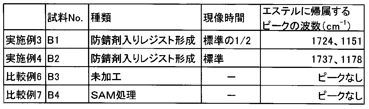
30×30mmの大きさのポリエチレンナフタレート(PEN)基材の一方主面上に、Cuからなる導電層を形成し、パターンレジストをラミネートし、露光、現像後、エッチング、剥離することで電極を形成した試料B1~B4を作製した。実施例3~4では、試料B1~B2に防錆剤入りレジストをラミネートし、露光、現像し、電極上に表面膜を形成した。比較例6として未加工の試料B3を用いた。比較例7は比較例5と同様の方法で、試料B4の電極に自己組織化単分子膜を形成した。
(2-1)試料の作製
30×30mmの大きさのポリエチレンナフタレート(PEN)基材の一方主面上に、Cuからなる導電層を形成し、パターンレジストをラミネートし、露光、現像後、エッチング、剥離することで電極を形成した試料B1~B4を作製した。実施例3~4では、試料B1~B2に防錆剤入りレジストをラミネートし、露光、現像し、電極上に表面膜を形成した。比較例6として未加工の試料B3を用いた。比較例7は比較例5と同様の方法で、試料B4の電極に自己組織化単分子膜を形成した。
(2-2)測定方法
試料B1~B4について、FT-IRスペクトルの測定を行った。測定には、Thermo Fisher Scientific社のNicolet(登録商標) iS(登録商標)10 FT-IR 分光装置を用いた。
試料B1~B4について、FT-IRスペクトルの測定を行った。測定には、Thermo Fisher Scientific社のNicolet(登録商標) iS(登録商標)10 FT-IR 分光装置を用いた。
(2-3)測定結果
測定結果を表2に示す。実施例3~4にはエステルに帰属するピークが確認されたが、比較例6~7では確認されなかった。したがって、実施例3~4に係る防錆剤入りレジストはエステルを含んでいることが分かった。
測定結果を表2に示す。実施例3~4にはエステルに帰属するピークが確認されたが、比較例6~7では確認されなかった。したがって、実施例3~4に係る防錆剤入りレジストはエステルを含んでいることが分かった。
(3)TFT特性
(3-1)試料の作製
実施例5;PEN基材の一方主面上にCuからなる導電層を形成し、パターンレジストをラミネートし、露光、現像、エッチング、剥離し、ソース電極およびドレイン電極、その他の配線を形成する。仕事関数及びFT-IRスペクトルの測定で用いたものと同じ防錆剤入りレジストをラミネート、露光、現像し、ソース電極およびドレイン電極上に表面膜を形成し、チャネル部を取り囲むように隔壁を形成した。次いで、ディスペンサーを使用して有機半導体インキを隔壁内に塗布した。さらに、ゲート絶縁膜を形成して、Cuを材料とするゲート電極を蒸着により形成し、試料C1とした。なお、使用した有機半導体インキはdif-TES-ADT 0.1wt% 溶媒;メシチレンであった。
(3-1)試料の作製
実施例5;PEN基材の一方主面上にCuからなる導電層を形成し、パターンレジストをラミネートし、露光、現像、エッチング、剥離し、ソース電極およびドレイン電極、その他の配線を形成する。仕事関数及びFT-IRスペクトルの測定で用いたものと同じ防錆剤入りレジストをラミネート、露光、現像し、ソース電極およびドレイン電極上に表面膜を形成し、チャネル部を取り囲むように隔壁を形成した。次いで、ディスペンサーを使用して有機半導体インキを隔壁内に塗布した。さらに、ゲート絶縁膜を形成して、Cuを材料とするゲート電極を蒸着により形成し、試料C1とした。なお、使用した有機半導体インキはdif-TES-ADT 0.1wt% 溶媒;メシチレンであった。
比較例8;PEN基材の一方主面上にCuからなる導電層を形成し、パターンレジストをラミネートし、露光、現像、エッチング、剥離し、ソース電極およびドレイン電極、その他の配線を形成した。ディスペンサーを使用して、チャネル部を取り囲むようにフッ素樹脂からなる隔壁を形成した。次いで、ディスペンサーを使用して有機半導体インキを隔壁内に塗布した。さらに、ゲート絶縁膜を形成して、Cuを材料とするゲート電極を蒸着により形成し、試料C2とした。
比較例9;PEN基材の一方主面上にCuからなる導電層を形成し、パターンレジストをラミネートし、露光、現像、エッチング、剥離し、ソース電極およびドレイン電極、その他の配線を形成する。ディスペンサーを使用して、チャネル部を取り囲むようにフッ素樹脂からなる隔壁を形成した。ソース電極およびドレイン電極をSAM処理液(10mM、ペンタフルオロベンゼンチオール、溶媒:イソプロピルアルコール)に5分間浸漬し、ソース電極およびドレイン電極に自己組織化単分子膜を形成した。次いで、ディスペンサーを使用して有機半導体インキを隔壁内に塗布した。さらに、ゲート絶縁膜を形成して、Cuを材料とするゲート電極を蒸着により形成し、試料C3とした。
(3-2)測定方法
ゲート電圧-ドレイン電流特性(伝達特性)はKEITHLEY社製、4200-SCS型 半導体パラメータ・アナライザによって測定した。伝達特性の測定条件は、ドレイン電圧が-20V、ゲート電圧の走査範囲が10V~-20Vであった。移動度は求められた伝達特性から算出した。
ゲート電圧-ドレイン電流特性(伝達特性)はKEITHLEY社製、4200-SCS型 半導体パラメータ・アナライザによって測定した。伝達特性の測定条件は、ドレイン電圧が-20V、ゲート電圧の走査範囲が10V~-20Vであった。移動度は求められた伝達特性から算出した。
(3-3)測定結果
表3に最大ドレイン電流(A)、移動度(cm2/V・sec)、On/Off比を測定した結果を示す。実施例5に係る試料C1の最大ドレイン電流は、比較例9に係る試料C3と同程度であった。また、移動度は、実施例5が比較例8~9の結果を上回ったことから、実施例5に係る試料C1はスイッチ速度の高い素子として作動することが期待できる。他方、試料C1のOn/Off比については改善の余地があることがわかった。
表3に最大ドレイン電流(A)、移動度(cm2/V・sec)、On/Off比を測定した結果を示す。実施例5に係る試料C1の最大ドレイン電流は、比較例9に係る試料C3と同程度であった。また、移動度は、実施例5が比較例8~9の結果を上回ったことから、実施例5に係る試料C1はスイッチ速度の高い素子として作動することが期待できる。他方、試料C1のOn/Off比については改善の余地があることがわかった。
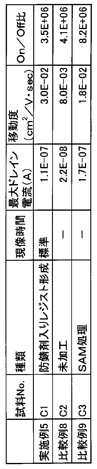
検証の結果から、防錆剤入りレジストを表面膜として用いた場合、SAM処理を行った場合と同程度の仕事関数が得られることがわかった。また、そのような表面膜は、FT-IRスペクトルのピークの位置からエステルを含むと考えられることがわかった。さらに、このような表面膜が形成された電極を有する能動素子は、最大ドレイン電流や移動度が高いものであった。
1:能動素子
2:基材
3:第1導電層
5:第1電極
6:第2電極
7、8:表面膜
9:有機半導体層
10:絶縁層
11:第3電極
12:レジスト層
13:隔壁
20:レジスト
20a、20b:マスク層
2:基材
3:第1導電層
5:第1電極
6:第2電極
7、8:表面膜
9:有機半導体層
10:絶縁層
11:第3電極
12:レジスト層
13:隔壁
20:レジスト
20a、20b:マスク層
Claims (8)
- 基材と、
該基材の一方主面上に隣り合って形成されている第1電極および第2電極と、
前記第1電極上および前記第2電極上に形成されている表面膜と、
前記基材の一方主面上であって、少なくとも前記第1電極と前記第2電極の間の領域を覆うように形成されている有機半導体層と、を有し、
前記表面膜は、pH10~12の現像液に45秒接触させた後のFT-IRスペクトルのピークが、(A)1000cm-1以上1300cm-1以下と、(B)1715cm-1以上1750cm-1以下の範囲にそれぞれ少なくとも一つ存在していることを特徴とする能動素子。 - 前記表面膜は、pH10~12の現像液に45秒接触させた後のFT-IRスペクトルのピークが、(A)1000cm-1以上1300cm-1以下と、(B1)1735cm-1以上1750cm-1以下の範囲にそれぞれ少なくとも一つ存在している請求項1に記載の能動素子。
- 前記表面膜の厚みが1nm以上40nm以下である請求項1または2に記載の能動素子。
- 前記表面膜は、前記第1電極および前記第2電極の向かい合う面上にもそれぞれ形成されている請求項1~3のいずれか一項に記載の能動素子。
- 前記第1電極および前記第2電極の材料がCuである請求項1~4のいずれか一項に記載の能動素子。
- 前記基材の一方主面上であって、前記有機半導体層よりも面方向外側に形成されている隔壁を有する請求項1~5のいずれか一項に記載の能動素子。
- 基材の一方主面上に隣り合う第1電極および第2電極を形成する工程と、
前記基材の一方主面上、前記第1電極および前記第2電極の一方主面上にレジスト層を形成する工程と、
前記レジスト層を現像液に接触させて、前記基材の一方主面上の前記第1電極と前記第2電極の間の領域のレジスト層と、前記第1電極および前記第2電極上のレジスト層の一部を除去することにより、第1電極上および第2電極上に表面膜を形成する工程と、
前記基材の一方主面上であって、少なくとも前記第1電極と前記第2電極の間の領域を覆うように有機半導体層を形成する工程と、を含むことを特徴とする能動素子の製造方法。 - レジスト層を形成する工程の後、前記レジスト層を前記現像液に接触させる工程の前に、前記第1電極および前記第2電極の間の領域の外側のレジスト層を露光する工程を含み、
前記レジスト層を前記現像液に接触させる工程により、前記基材の一方主面上の前記第1電極および前記第2電極の間の領域の外側に隔壁を形成する請求項7に記載の能動素子の製造方法。
Applications Claiming Priority (2)
| Application Number | Priority Date | Filing Date | Title |
|---|---|---|---|
| JP2016-119382 | 2016-06-15 | ||
| JP2016119382A JP2017224739A (ja) | 2016-06-15 | 2016-06-15 | 能動素子、および能動素子の製造方法 |
Publications (1)
| Publication Number | Publication Date |
|---|---|
| WO2017217080A1 true WO2017217080A1 (ja) | 2017-12-21 |
Family
ID=60663111
Family Applications (1)
| Application Number | Title | Priority Date | Filing Date |
|---|---|---|---|
| PCT/JP2017/013993 Ceased WO2017217080A1 (ja) | 2016-06-15 | 2017-04-03 | 能動素子、および能動素子の製造方法 |
Country Status (3)
| Country | Link |
|---|---|
| JP (1) | JP2017224739A (ja) |
| TW (1) | TW201813145A (ja) |
| WO (1) | WO2017217080A1 (ja) |
Families Citing this family (1)
| Publication number | Priority date | Publication date | Assignee | Title |
|---|---|---|---|---|
| TWI727752B (zh) * | 2020-04-21 | 2021-05-11 | 友達光電股份有限公司 | 主動元件 |
Citations (3)
| Publication number | Priority date | Publication date | Assignee | Title |
|---|---|---|---|---|
| JP2012234923A (ja) * | 2011-04-28 | 2012-11-29 | Dainippon Printing Co Ltd | 薄膜トランジスタ基板の製造方法およびトップゲート構造薄膜トランジスタ基板 |
| WO2013046547A1 (ja) * | 2011-09-26 | 2013-04-04 | パナソニック株式会社 | 有機薄膜トランジスタ |
| WO2013061528A1 (ja) * | 2011-10-24 | 2013-05-02 | パナソニック株式会社 | 薄膜トランジスタ、有機el発光素子及び薄膜トランジスタの製造方法 |
-
2016
- 2016-06-15 JP JP2016119382A patent/JP2017224739A/ja active Pending
-
2017
- 2017-04-03 WO PCT/JP2017/013993 patent/WO2017217080A1/ja not_active Ceased
- 2017-06-14 TW TW106119727A patent/TW201813145A/zh unknown
Patent Citations (3)
| Publication number | Priority date | Publication date | Assignee | Title |
|---|---|---|---|---|
| JP2012234923A (ja) * | 2011-04-28 | 2012-11-29 | Dainippon Printing Co Ltd | 薄膜トランジスタ基板の製造方法およびトップゲート構造薄膜トランジスタ基板 |
| WO2013046547A1 (ja) * | 2011-09-26 | 2013-04-04 | パナソニック株式会社 | 有機薄膜トランジスタ |
| WO2013061528A1 (ja) * | 2011-10-24 | 2013-05-02 | パナソニック株式会社 | 薄膜トランジスタ、有機el発光素子及び薄膜トランジスタの製造方法 |
Also Published As
| Publication number | Publication date |
|---|---|
| TW201813145A (zh) | 2018-04-01 |
| JP2017224739A (ja) | 2017-12-21 |
Similar Documents
| Publication | Publication Date | Title |
|---|---|---|
| CN102224580B (zh) | 薄膜晶体管制造方法、薄膜晶体管以及电子装置 | |
| US9685558B2 (en) | Flexible electronic device having adhesive function and method of manufacturing the same | |
| CN107408510B (zh) | 薄膜晶体管、薄膜晶体管的制造方法及使用了薄膜晶体管的图像显示装置 | |
| CN101075658A (zh) | 电极的形成方法和有机薄膜晶体管及显示装置 | |
| CN102867914A (zh) | 电子器件和半导体器件的制造方法 | |
| CN107078164A (zh) | 薄膜晶体管及其制造方法 | |
| WO2017217080A1 (ja) | 能動素子、および能動素子の製造方法 | |
| JP5332145B2 (ja) | 積層構造体、電子素子、電子素子アレイ及び表示装置 | |
| JP4443944B2 (ja) | トランジスタとその製造方法 | |
| CN108376740A (zh) | 复合沟道晶体管及其制备方法 | |
| WO2017056720A1 (ja) | 能動素子、および能動素子の製造方法 | |
| JP4652866B2 (ja) | 有機トランジスタ | |
| US20210225884A1 (en) | Array substrate, manufacturing method thereof, and display panel | |
| JP6241573B2 (ja) | 電子デバイスの製造方法 | |
| JP6088012B1 (ja) | 能動素子、および能動素子の製造方法 | |
| JP2020161523A (ja) | 有機半導体薄膜トランジスタ素子 | |
| JP6303358B2 (ja) | 薄膜トランジスタ | |
| JP6492523B2 (ja) | 有機半導体薄膜トランジスタ素子 | |
| JP6446850B2 (ja) | 薄膜トランジスタ | |
| JP2019096727A (ja) | 薄膜トランジスタ、薄膜トランジスタの製造方法および画像表示装置 | |
| JP6620556B2 (ja) | 機能材料の積層方法及び機能材料積層体 | |
| JP2020096006A (ja) | 薄膜トランジスタ | |
| KR100839301B1 (ko) | 유기박막 트랜지스터 및 그 제조방법 | |
| JP2015198165A (ja) | 薄膜トランジスタ及びその製造方法 | |
| JP2017195315A (ja) | 薄膜トランジスタ |
Legal Events
| Date | Code | Title | Description |
|---|---|---|---|
| 121 | Ep: the epo has been informed by wipo that ep was designated in this application |
Ref document number: 17812986 Country of ref document: EP Kind code of ref document: A1 |
|
| NENP | Non-entry into the national phase |
Ref country code: DE |
|
| 122 | Ep: pct application non-entry in european phase |
Ref document number: 17812986 Country of ref document: EP Kind code of ref document: A1 |