WO2017212926A1 - 熱電変換材料及び熱電変換モジュール - Google Patents
熱電変換材料及び熱電変換モジュール Download PDFInfo
- Publication number
- WO2017212926A1 WO2017212926A1 PCT/JP2017/019482 JP2017019482W WO2017212926A1 WO 2017212926 A1 WO2017212926 A1 WO 2017212926A1 JP 2017019482 W JP2017019482 W JP 2017019482W WO 2017212926 A1 WO2017212926 A1 WO 2017212926A1
- Authority
- WO
- WIPO (PCT)
- Prior art keywords
- thermoelectric conversion
- thermoelectric
- conversion material
- merit
- chemical formula
- Prior art date
- Legal status (The legal status is an assumption and is not a legal conclusion. Google has not performed a legal analysis and makes no representation as to the accuracy of the status listed.)
- Ceased
Links
Images

Classifications
-
- H—ELECTRICITY
- H10—SEMICONDUCTOR DEVICES; ELECTRIC SOLID-STATE DEVICES NOT OTHERWISE PROVIDED FOR
- H10N—ELECTRIC SOLID-STATE DEVICES NOT OTHERWISE PROVIDED FOR
- H10N10/00—Thermoelectric devices comprising a junction of dissimilar materials, i.e. devices exhibiting Seebeck or Peltier effects
- H10N10/80—Constructional details
- H10N10/85—Thermoelectric active materials
- H10N10/851—Thermoelectric active materials comprising inorganic compositions
- H10N10/852—Thermoelectric active materials comprising inorganic compositions comprising tellurium, selenium or sulfur
-
- C—CHEMISTRY; METALLURGY
- C01—INORGANIC CHEMISTRY
- C01G—COMPOUNDS CONTAINING METALS NOT COVERED BY SUBCLASSES C01D OR C01F
- C01G33/00—Compounds of niobium
- C01G33/006—Compounds containing niobium, with or without oxygen or hydrogen, and containing two or more other elements
-
- C—CHEMISTRY; METALLURGY
- C01—INORGANIC CHEMISTRY
- C01G—COMPOUNDS CONTAINING METALS NOT COVERED BY SUBCLASSES C01D OR C01F
- C01G35/00—Compounds of tantalum
- C01G35/006—Compounds containing tantalum, with or without oxygen or hydrogen, and containing two or more other elements
-
- H—ELECTRICITY
- H10—SEMICONDUCTOR DEVICES; ELECTRIC SOLID-STATE DEVICES NOT OTHERWISE PROVIDED FOR
- H10N—ELECTRIC SOLID-STATE DEVICES NOT OTHERWISE PROVIDED FOR
- H10N10/00—Thermoelectric devices comprising a junction of dissimilar materials, i.e. devices exhibiting Seebeck or Peltier effects
- H10N10/10—Thermoelectric devices comprising a junction of dissimilar materials, i.e. devices exhibiting Seebeck or Peltier effects operating with only the Peltier or Seebeck effects
- H10N10/17—Thermoelectric devices comprising a junction of dissimilar materials, i.e. devices exhibiting Seebeck or Peltier effects operating with only the Peltier or Seebeck effects characterised by the structure or configuration of the cell or thermocouple forming the device
-
- C—CHEMISTRY; METALLURGY
- C01—INORGANIC CHEMISTRY
- C01P—INDEXING SCHEME RELATING TO STRUCTURAL AND PHYSICAL ASPECTS OF SOLID INORGANIC COMPOUNDS
- C01P2006/00—Physical properties of inorganic compounds
- C01P2006/32—Thermal properties
-
- C—CHEMISTRY; METALLURGY
- C01—INORGANIC CHEMISTRY
- C01P—INDEXING SCHEME RELATING TO STRUCTURAL AND PHYSICAL ASPECTS OF SOLID INORGANIC COMPOUNDS
- C01P2006/00—Physical properties of inorganic compounds
- C01P2006/40—Electric properties
Definitions
- the present invention relates to a thermoelectric conversion material having an excellent thermoelectric figure of merit ZT and a thermoelectric conversion module formed using the thermoelectric conversion material.
- thermoelectric conversion is a technique for converting heat energy and electrical energy to each other using a solid thermoelectric conversion element.
- a technique for converting thermal energy into electrical energy is called thermoelectric generation, and is based on the Seebeck effect, which is one of the thermoelectric effects.
- thermoelectric power generation the temperature difference between both ends of the thermoelectric conversion material is directly converted into electric energy.
- the conversion from electrical energy to thermal energy originates from the Peltier effect, which is another thermoelectric effect, and is applied to cooling and precision temperature control.
- the conversion from electrical energy derived from the Peltier effect to thermal energy is referred to as Peltier cooling.
- Peltier cooling uses a phenomenon in which one end of the thermoelectric conversion material is cooled when a current is passed through the thermoelectric conversion material. The advantage of this Peltier cooling is that it does not require a refrigerant such as Freon gas for cooling and that the cooling temperature can be precisely controlled based on current control.
- thermoelectric conversion material carriers that carry charge is holes
- N-type thermoelectric conversion materials carriers that carry charges are electrons
- ZT thermoelectric figure of merit
- S the Seebeck coefficient of the thermoelectric conversion material
- T the absolute temperature
- ⁇ the electrical resistivity of the thermoelectric conversion material
- ⁇ the thermal conductivity of the thermoelectric conversion material.
- thermoelectric figure of merit ZT the higher the conversion efficiency between heat energy and electric energy, and the better the performance of the thermoelectric conversion material. That is, by increasing the conversion efficiency, it is possible to extract more electric power from unused thermal energy using the thermoelectric conversion and to suppress power consumption during cooling.
- thermoelectric conversion material a chemical composition is Cu 26-x M x A 2 E 6 S 32 (where M is a metal material containing at least one of Mn, Fe, Co, Ni, and Zn).
- A represents a metal material containing at least one of V, Nb and Ta
- E represents a metal material containing at least one of Si, Ge and Sn
- x represents a numerical value of 0 to 5
- the corusite has a large thermoelectric figure of merit ZT of up to 0.73 at 390 ° C., and is composed mainly of copper (Cu) and sulfur (S) with low toxicity and a large amount of crustal reserves. Suitable as thermoelectric conversion material. Therefore, if the thermoelectric figure of merit ZT of the corusite is improved and the conversion efficiency is increased, a more useful thermoelectric conversion material and thermoelectric conversion module can be provided.
- thermoelectric figure of merit ZT As a method of improving the thermoelectric figure of merit ZT in the corusite, a method of eliminating Sn from corusite having a basic composition of Cu 26 V 2 Sn 6 S 32 has been proposed (see Non-Patent Document 3). According to this proposal, the thermoelectric figure of merit ZT of Cu 26 V 2 Sn 5.5 S 32 introduced with Sn vacancies is 0.62 at 387 ° C., and the thermoelectric of Cu 26 V 2 Sn 6 S 32 without introducing Sn vacancies. The figure of merit ZT is set to 0.56.
- thermoelectric figure of merit ZT 0.73
- K. Suekuni, F. S. Kim, and T. Takabatake, ⁇ Tunable electronic properties and low thermal conductivity in synthetic colusites Cu26-xZnxV2M6S32 (M Ge, Sn) '', Journal of3Apps 5 pages, August 2014.
- the present invention solves the above problems in the prior art, and provides a thermoelectric conversion material having a low environmental load and an excellent thermoelectric performance index ZT, and a thermoelectric conversion module formed using the thermoelectric conversion material. Is an issue.
- thermoelectric figure of merit ZT it is assumed that the electrical resistivity ⁇ is reduced and the thermoelectric figure of merit ZT is improved.
- the method of introducing Sn deficiency (see Non-Patent Document 3) aims to improve the thermoelectric figure of merit ZT under such assumption, but even if Sn deficiency is introduced, the effect of improving the thermoelectric figure of merit ZT is slight. In other words, sufficient effects are not obtained.
- Nb or Ta of the same group element is selected instead of V in Cu 26 V 2 Sn 6 S 32 , the valence of corusite No significant change in the thermoelectric figure of merit ZT is expected.
- thermoelectric figure of merit, ZT far exceeded expectations, for example, reaching 0.78 in a temperature environment of 389 ° C.
- the highest value is 0.73
- the thermoelectric figure of merit ZT of 0.78 is composed of Cu 26 Nb 2 Sn 5.5 S 32 . It is shown that the thermoelectric conversion material to be used has the best performance in the world at this stage.
- thermoelectric figure of merit ZT of Cu 26 Nb 2 Sn 6 S 32 that does not introduce Sn deficiency is about 0.52 at most. Unlike V, Cu 26 Nb 2 of the basic composition is used in the case of Nb. It was confirmed that the introduction of Sn deficiency into Sn 6 S 32 improved the thermoelectric figure of merit ZT by 0.26. Also, the thermoelectric figure of merit ZT of Cu 26 Ta 2 Sn 5.5 S 32 in which Ta is selected from the group element instead of V and Sn deficiency is introduced is also compared with that of Cu 26 Ta 2 Sn 6 S 32 of the basic composition. Thus, a significant improvement in the thermoelectric figure of merit ZT was confirmed.
- V, Nb, and Ta are the same group elements, and therefore have the same ionic state.
- the number of electrons of Nb of atomic number 41 is about twice as large as that of V of atomic number 23, and the number of electrons of Ta of atomic number 73 is about three times as large.
- the corrosite containing Nb and Ta and the corusite containing V have different physical and chemical properties.
- the thermoelectric figure of merit ZT is greatly improved by Sn defects when the homologous elements Nb and Ta are selected instead of V.
- thermoelectric conversion material which is a compound represented by the following chemical formula (1).
- M represents a metal material containing at least one of Mn, Fe, Co, Ni and Zn
- A represents a metal material containing at least one of Nb and Ta
- E represents a metal material containing at least one of Si, Ge and Sn
- x represents a numerical value of 0 or more and 4 or less
- y represents a numerical value greater than 0 and 1 or less.
- thermoelectric conversion material according to any one of ⁇ 1> to ⁇ 2>, wherein a numerical value represented by y in the chemical formula (1) is greater than 0 and 0.5 or less.
- ⁇ 4> The thermoelectric conversion material according to any one of ⁇ 1> to ⁇ 3>, wherein the metal material represented by E in the chemical formula (1) includes at least one of Sn and Ge.
- ⁇ 5> The thermoelectric conversion material according to any one of ⁇ 1> to ⁇ 4>, wherein the thermoelectric figure of merit ZT exhibits a value greater than 0.73 in a temperature environment of 365 ° C. to 400 ° C.
- thermoelectric conversion module comprising a thermoelectric conversion material layer formed of the thermoelectric conversion material according to any one of ⁇ 1> to ⁇ 5>.
- thermoelectric conversion material having an excellent thermoelectric figure of merit ZT and the thermoelectric conversion formed using the thermoelectric conversion material Modules can be provided.
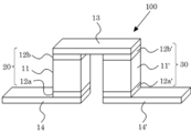
- thermoelectric conversion element It is explanatory drawing for demonstrating the structure of a thermoelectric conversion element. It is a figure for demonstrating the structure of a thermoelectric conversion module.
- thermoelectric conversion material The thermoelectric conversion material of the present invention is a compound represented by the following chemical formula (1).
- M represents a metal material containing at least one of Mn, Fe, Co, Ni and Zn
- A represents a metal material containing at least one of Nb and Ta
- E represents a metal material containing at least one of Si, Ge and Sn
- x represents a numerical value of 0 or more and 4 or less
- y represents a numerical value greater than 0 and 1 or less.
- the metal material indicated by M in the chemical formula (1) is a transition element (M 2+ ) that takes a divalent cation state, and Cu in the compound depends on the numerical value indicated by x in the chemical formula (1). Replaced with (Cu + ). By this substitution, it is possible to adjust the degree of valence reduction of the compound as well as the selection of the numerical value represented by y in the chemical formula (1).
- the valence adjustment of the compound can be easily performed by adjusting the value of x and the value of y.
- the type of the compound according to the purpose can be easily obtained.
- the numerical value indicated by x in the chemical formula (1) is preferably 0.
- the metal material represented by A in the chemical formula (1) is a transition element (A 5+ ) belonging to Group 5 of the periodic table, which takes a pentavalent cation state, and has more electrons than V of the group element. It is a transition element.
- the thermoelectric figure of merit ZT is greatly improved when defects are introduced into the composition of the metal material indicated by E in the chemical formula (1) with respect to the corrusite having the basic composition. Can be made.
- the metal material represented by E in the chemical formula (1) is not limited to Sn, and the thermoelectric conversion material includes the compound containing at least one of Nb and Ta in the metal material represented by A in the chemical formula (1).
- the periodic table Ge and Si are included, which belongs to the same group 14 as Sn and takes the same ion state as Sn.
- the numerical value represented by y in the chemical formula (1) is set to be larger than 0 and equal to or smaller than 1 from the viewpoint of lowering the electrical resistivity ⁇ and thus obtaining a high thermoelectric figure of merit ZT.
- a numerical value shown by y in the said Chemical formula (1) it is preferable that it is more than 0 and 0.5 or less. That is, when the numerical value represented by y is a relatively large numerical value exceeding 0.5 and the valence of the compound is decreased, the electrical resistivity ⁇ is decreased and the Seebeck coefficient S is also relatively decreased. A decrease in the Seebeck coefficient S causes a decrease in the thermoelectric figure of merit ZT. Therefore, from the viewpoint of achieving both a low electrical resistivity ⁇ and a high Seebeck coefficient S and obtaining a higher thermoelectric figure of merit ZT, it is more preferably greater than 0 and 0.5 or less.
- thermoelectric conversion material there is no restriction
- each elemental element constituting the compound is weighed, and then vacuum sealed in a quartz tube and heated and melted.
- the compound in which Cu is partially substituted with the metal material represented by M in the chemical formula (1) is obtained, and when any y is designated, the metal represented by E in the chemical formula (1) is obtained.
- the compound in which a defect is introduced into the material is synthesized.
- the high density polycrystal of the said compound is obtained by performing hot press sintering after grind
- thermoelectric conversion module The thermoelectric conversion module of the present invention has a thermoelectric conversion material layer formed of the thermoelectric conversion material of the present invention.
- a method for forming the thermoelectric conversion material layer is not particularly limited, and the thermoelectric conversion material layer can be formed according to a known formation method, for example, a formation method described in Patent Document 1, Non-Patent Documents 1 to 3, and the like.
- thermoelectric conversion module is not particularly limited as long as it has the thermoelectric conversion material layer, and can be appropriately selected from the configurations of known thermoelectric conversion modules.
- a known thermoelectric conversion module a P-type thermoelectric conversion element (a carrier carrying charge is a hole) formed of a P-type thermoelectric conversion material and an N-type thermoelectric conversion material (a carrier carrying charge is an electron) N
- the thermoelectric conversion element has a pair, and the pair of thermoelectric conversion elements is arranged in a bowl shape.
- the thermoelectric conversion module also functions as a pair of the thermoelectric conversion elements, but may be configured to include a plurality of pairs of thermoelectric conversion elements from the viewpoint of high performance.
- thermoelectric conversion module when the thermoelectric conversion module is composed of a P-type thermoelectric conversion element and an N-type thermoelectric conversion element, the thermoelectric conversion module of the present invention is dominated by carriers having positive charges as electrical carriers.
- the thermoelectric conversion element in which the thermoelectric conversion material layer is formed with the thermoelectric conversion material of the present invention is a P-type thermoelectric conversion element.
- N-type thermoelectric conversion element it can select from a well-known thing suitably and can be used.
- thermoelectric conversion element in which the thermoelectric conversion material layer is formed of the thermoelectric conversion material of the present invention is not particularly limited, and a thermoelectric conversion material layer formed of the thermoelectric conversion material and And an electrode layer disposed in a state of being joined to the thermoelectric conversion material layer.
- the electrode layer is not particularly limited, but from the viewpoint of chemical stability with the thermoelectric conversion material layer (corusite), It is preferably formed of an electrode material containing at least one of Ti, Pt and Au. Among them, Au is particularly preferable from the viewpoint of obtaining a lower electric resistance. Further, the electrode material is not particularly limited, and those manufactured by a known manufacturing method or commercially available products can be used. When the electrode layer is formed, the electrode material is in a state of powder, foil, plate, or the like. What was processed can be used.
- thermoelectric conversion element the said P-type thermoelectric conversion element
- thermoelectric conversion material layer was formed with the said thermoelectric conversion material of this invention
- a well-known formation method for example, a patent It can be formed according to the formation methods described in Document 1, Non-Patent Documents 1 to 3, and the like.
- FIG. 1 is an explanatory diagram for explaining a configuration of a thermoelectric conversion element.
- the thermoelectric conversion element 10 shown in FIG. 1 has the same element configuration as a general thermoelectric conversion element.
- the thermoelectric conversion element 10 is configured such that the thermoelectric conversion material layer 1 is sandwiched between two electrode layers 2a and 2b.
- the electrode layers 2a and 2b electrically and thermally connect the thermoelectric conversion material layer 1 and a bonding electrode to be described later to transfer current and heat well, while the thermoelectric conversion material layer 1 and the bonding electrode It has a role of suppressing reaction and a role of relaxing stress between the thermoelectric conversion material layer 1 and the bonding electrode.
- thermoelectric conversion module 100 shown in FIG. 2 is the same as the module structure of a general thermoelectric conversion module.
- the thermoelectric conversion module 100 includes two thermoelectric conversion elements, that is, a P-type thermoelectric conversion element 20 and an N-type thermoelectric conversion element 30 that are made of the thermoelectric conversion material of the present invention, and an upper portion between the two thermoelectric conversion elements. It is composed of one upper junction electrode 13 disposed so as to pass and lower junction electrodes 14 and 14 'respectively disposed below the P-type thermoelectric conversion element 20 and the N-type thermoelectric conversion element 30, as shown in FIG. Thus, the whole has a bowl shape.
- the P-type thermoelectric conversion element 20 has a configuration in which a thermoelectric conversion material layer 11 is sandwiched between two electrode layers 12a and 12b, similarly to the thermoelectric conversion element 10.
- the N-type thermoelectric conversion element 30 a known N-type conversion element can be appropriately selected. For example, the thermoelectric conversion material layer 11 ′ is sandwiched between two electrode layers 12 a ′ and 12 b ′.
- the thermoelectric conversion module 100 can be used as a thermoelectric power generation module that generates a potential difference between the lower bonding electrodes 14-14 ′ when the upper bonding electrode 13 side is heated and the lower bonding electrodes 14, 14 ′ are cooled. it can. Further, in the thermoelectric conversion module 100, a positive voltage is applied to the lower bonding electrode 14 ′ and a negative voltage is applied to the lower bonding electrode 14 to introduce a current into the module from the lower bonding electrode 14 ′. When a voltage is applied so as to be transmitted, a heat absorption phenomenon occurs on the upper bonding electrode 13 side, a heat dissipation phenomenon occurs on the lower bonding electrodes 14 and 14 'side, and the temperature of the target in contact with the upper bonding electrode 13 is increased.
- thermoelectric conversion module of this invention can be used as a Peltier cooling module to lower.
- FIG. 2 the module structure shown in FIG. 2 shows an example of the structure of the said thermoelectric conversion module of this invention, and others are well-known. The configuration of the thermoelectric conversion module is not excluded.
- thermoelectric conversion material of the present invention examples of the thermoelectric conversion material of the present invention will be described. However, the idea of the present invention is not limited to these examples.
- Example 1 First, Cu (1.409 g), Nb (0.159 g), Sn (0.557 g), and S (0.875 g) as raw materials are vacuum sealed in a quartz tube and melted at 1,050 ° C. About 3 g of a polycrystalline sample having a composition of Cu 26 Nb 2 Sn 5.5 S 32 was obtained. The production phase of the obtained polycrystalline sample was confirmed by powder X-ray diffraction. Next, the obtained polycrystalline sample of Cu 26 Nb 2 Sn 5.5 S 32 was crushed into a powder and subjected to hot press sintering to obtain a thermoelectric conversion material according to Example 1 as a high-density polycrystalline sintered body. Manufactured.
- thermoelectric conversion material according to Comparative Example 1 From raw materials, Cu (1.409 g), Nb (0.159 g), Sn (0.557 g), S (0.875 g) to Cu (1.386 g), Nb (0.156 g), Sn (0.599 g) ), S (0.861 g), and the thermoelectric conversion material according to Comparative Example 1 was obtained in the same manner as in Example 1 except that a polycrystalline sample having a composition of Cu 26 Nb 2 Sn 6 S 32 was obtained. Manufactured. The production phase of the obtained polycrystalline sample was confirmed by powder X-ray diffraction.
- thermoelectric figure of merit ZT calculated from is shown in Table 1 below.
- Table 2 the measurement results of Seebeck coefficient S, electrical resistivity ⁇ , and thermal conductivity ⁇ measured in the same manner as the thermoelectric conversion material according to Example 1, and this measurement
- the thermoelectric figure of merit ZT calculated from the results is shown in Table 2 below.
- the metal material represented by A in the chemical formula (1) is Nb
- the metal material represented by E is Sn
- y a numerical value represented by defects
- thermoelectric conversion material according to Example 1 in which Sn deficiency was introduced with 0.5 as the electrical resistivity ⁇ , compared with the thermoelectric conversion material according to Comparative Example 1 manufactured in the same manner except that Sn deficiency was not introduced. It can be seen that the thermoelectric figure of merit ZT is increased. Moreover, the improvement effect of the thermoelectric figure of merit ZT due to the introduction of Sn deficiency when compared under the same temperature condition is 0.26 at maximum, and the thermoelectric conversion material according to Example 1 is related to Comparative Example 1. Compared with the thermoelectric conversion material, a dramatic improvement in the thermoelectric performance index ZT is confirmed.
- thermoelectric figure of merit ZT of the thermoelectric conversion material according to Example 1 in which Sn deficiency was introduced was the same as that of Cu 26 V 2 Sn 5.5 S 32 in Non-Patent Document 3 in which Sn deficiency was also introduced. Compared to the value 0.62 of the figure of merit ZT, it is about 30% higher.
- thermoelectric performance index ZT of the thermoelectric conversion material according to Example 1 due to the introduction of Sn deficiency
- thermoelectric performance index ZT is improved by 0.26
- thermoelectric figure of merit ZT is improved by 0.06
- Example 2 The raw materials are Cu (1.409 g), Nb (0.159 g), Sn (0.557 g), S (0.875 g) to Cu (1.4414 g), Ta (0.3163 g), Ge (0.3485 g). ), S (0.8932 g), and the thermoelectric conversion according to Example 2 was performed in the same manner as in Example 1 except that a polycrystalline sample having a composition of Cu 26 Ta 2 Ge 5.5 S 32 was obtained. The material was manufactured. The production phase of the obtained polycrystalline sample was confirmed by powder X-ray diffraction.
- thermoelectric conversion material From Cu (1.4414 g), Ta (0.3163 g), Ge (0.3485 g), S (0.8932 g) to Cu (1.426 g), Ta (0.313 g), Ge (0.375 g) ), S (0.886 g), and a thermoelectric conversion material according to Comparative Example 2 was obtained in the same manner as in Example 2 except that a polycrystalline sample having a composition of Cu 26 Ta 2 Ge 6 S 32 was obtained. Manufactured. The production phase of the obtained polycrystalline sample was confirmed by powder X-ray diffraction.
- thermoelectric figure of merit ZT is shown in Table 3 below.
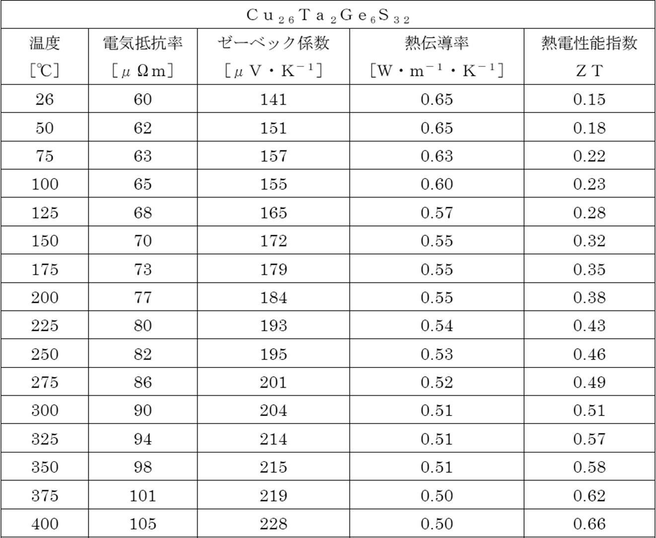
- each measurement result of Seebeck coefficient S, electrical resistivity ⁇ , and thermal conductivity ⁇ measured in the same manner as the thermoelectric conversion material according to Example 1 for the thermoelectric conversion material according to Comparative Example 2 and this measurement The thermoelectric figure of merit ZT calculated from the results is shown in Table 4 below.
- a maximum of 0.79 was shown below.
- a thermoelectric figure of merit ZT of 0.79 indicates that the thermoelectric conversion material according to Example 3 has the world's highest level of performance at this stage.
- the metal material represented by A in the chemical formula (1) is Ta
- the metal material represented by E is Ge
- thermoelectric conversion material according to Example 2 in which Sn deficiency was introduced with 0.5 as the electrical resistivity ⁇ , compared with the thermoelectric conversion material according to Comparative Example 2 manufactured in the same manner except that Sn deficiency was not introduced. It can be seen that the thermoelectric figure of merit ZT is increased. Moreover, the improvement effect of the thermoelectric figure of merit ZT due to the introduction of Sn deficiency when compared under the same temperature condition is 0.13 at the maximum, and the thermoelectric conversion material according to Example 2 is related to Comparative Example 2. Compared with the thermoelectric conversion material, a dramatic improvement in the thermoelectric performance index ZT is confirmed.
- thermoelectric performance index ZT value 0.79 of the thermoelectric conversion material according to Example 2 in which Ge deficiency is introduced is the thermoelectric performance of Cu 26 V 2 Sn 5.5 S 32 in Non-Patent Document 3 in which Sn deficiency is introduced. It is about 30% higher than the index ZT value of 0.62, and by changing the metal material represented by A in the chemical formula (1) from V to Nb, a significant improvement in the thermoelectric performance index ZT is confirmed. .
- the improvement effect of the thermoelectric performance index ZT of the thermoelectric conversion material according to Example 2 accompanying the introduction of Ge deficiency is a non-patent document accompanying the introduction of Sn deficiency.
- the thermoelectric performance index ZT is improved 0.06
- Example 3 The raw materials were Cu (1.409 g), Nb (0.159 g), Sn (0.557 g), S (0.875 g) to Cu (1.3209 g), Ta (0.2898 g), Sn (0.5700 g). ), S (0.8213 g), and the thermoelectric conversion according to Example 3 was performed in the same manner as in Example 1 except that a polycrystalline sample having a composition of Cu 26 Ta 2 Sn 5.5 S 32 was obtained. The material was manufactured. The production phase of the obtained polycrystalline sample was confirmed by powder X-ray diffraction.
- thermoelectric conversion material From Cu (1.3209 g), Ta (0.2898 g), Sn (0.5700 g), S (0.8213 g) to Cu (1.5638 g), Ta (0.343 g), Sn (0.6198 g) ), S (0.9725 g), and a thermoelectric conversion material according to Comparative Example 3 was obtained in the same manner as in Example 3 except that a polycrystalline sample having a composition of Cu 26 Ta 2 Sn 6 S 32 was obtained. Manufactured. The production phase of the obtained polycrystalline sample was confirmed by powder X-ray diffraction.
- thermoelectric figure of merit ZT is shown in Table 5 below. Further, the measurement results of Seebeck coefficient S, electrical resistivity ⁇ , and thermal conductivity ⁇ measured for the thermoelectric conversion material according to Comparative Example 3 in the same manner as the thermoelectric conversion material according to Example 1, and this measurement The thermoelectric figure of merit ZT calculated from the results is shown in Table 6 below.
- a maximum of 0.97 was shown below.
- a thermoelectric figure of merit ZT of 0.97 indicates that the thermoelectric conversion material according to Example 3 has the world's highest level of performance at this stage.
- a metal material represented by A is Ta
- a metal material represented by E is Sn
- y a numerical value represented by defects
- thermoelectric conversion material according to Example 3 in which Sn deficiency was introduced with 0.5 as the electrical resistivity ⁇ as compared with the thermoelectric conversion material according to Comparative Example 3 manufactured in the same manner except that Sn deficiency was not introduced. It can be seen that the thermoelectric figure of merit ZT is increased. Moreover, the improvement effect of the thermoelectric figure of merit ZT by introduction of Sn deficiency when compared under the same temperature condition was recorded as 0.19 at the maximum, and the thermoelectric conversion material according to Example 3 was related to Comparative Example 3. Compared with the thermoelectric conversion material, a dramatic improvement in the thermoelectric performance index ZT is confirmed.
- thermoelectric performance index ZT of the thermoelectric conversion material according to Example 3 in which Sn deficiency was introduced was the thermoelectric performance of Cu 26 V 2 Sn 5.5 S 32 in Non-Patent Document 3 in which Sn deficiency was introduced. It is about 50% higher than the index ZT value of 0.62, and by changing the metal material represented by A in the chemical formula (1) from V to Ta, a significant improvement in the thermoelectric performance index ZT is confirmed. .
- the effect of improving the thermoelectric figure of merit ZT of the thermoelectric conversion material according to Example 3 accompanying the introduction of Sn deficiency is a non-patent document accompanying the introduction of Sn deficiency.
- thermoelectric performance index ZT is improved by 0.06
- Example 4 From raw materials, Cu (1.409 g), Nb (0.159 g), Sn (0.557 g), S (0.875 g) to Cu (1.5198 g), Nb (0.1718 g), Ge (0.3678 g) ), S (0.9438 g), and the thermoelectric conversion according to Example 4 was performed in the same manner as in Example 1 except that a polycrystalline sample having a composition of Cu 26 Nb 2 Ge 5.5 S 32 was obtained. The material was manufactured. The production phase of the obtained polycrystalline sample was confirmed by powder X-ray diffraction.
- thermoelectric figure of merit ZT is shown in Table 7 below.
- the thermoelectric conversion material according to Example 4 is the same compound as the thermoelectric conversion material according to Example 1 except that the metal material represented by E in the chemical formula (1) is changed from Sn to Ge. It is confirmed that even if the metal material indicated by E in (1) is changed to Ge, a high thermoelectric figure of merit ZT can be obtained.
- thermoelectric figure of merit ZT of the thermoelectric conversion material according to Example 4 in which Ge deficiency is introduced is the thermoelectric performance of Cu 26 V 2 Sn 5.5 S 32 in Non-Patent Document 3 in which Sn deficiency is introduced. It is about 20% higher than the value 0.62 of the index ZT, and a significant improvement in the thermoelectric performance index ZT is confirmed by changing the metal material represented by A in the chemical formula (1) from V to Nb. .
- thermoelectric figure of merit of sintered body of Cu 26 V 2 Sn 5.5 S 32 and Cu 26 V 2 Sn 6 S 32 are each Cu 26 V 2 Sn 5.5 S at 32 387 ° C. 0.62 for Cu 26 V 2 Sn 6 S 32 and 0.56 at 391 ° C., and the effect of improving the thermoelectric figure of merit ZT by introducing Sn deficiency into Cu 26 V 2 Sn 6 S 32 Is about 0.06. That is, no significant improvement in the thermoelectric figure of merit ZT due to Sn deficiency is observed in corusite where the metal material represented by A in the chemical formula (1) is V.
- thermoelectric figure of merit ZT is expected to be equal.
- each of the thermoelectric conversion materials according to Examples 1 to 4 in which one of Nb and Ta is selected exhibits a thermoelectric figure of merit ZT that is several orders of magnitude higher than that of corusite described in Non-Patent Document 3 in which V is selected.
- each of the thermoelectric conversion materials according to Examples 1 to 3 is larger than the thermoelectric conversion material described in Patent Document 1 according to the report example of the highest thermoelectric figure of merit ZT among those reported in the past.
- a conversion performance index ZT is obtained, and the thermoelectric conversion material according to the present invention has an excellent thermoelectric performance index ZT, contrary to the previous expectation.
Landscapes
- Chemical & Material Sciences (AREA)
- Organic Chemistry (AREA)
- Inorganic Chemistry (AREA)
- Powder Metallurgy (AREA)
- Inorganic Compounds Of Heavy Metals (AREA)
Abstract
【課題】環境負荷が低く、かつ、優れた熱電性能指数ZTを有する熱電変換材料及び前記熱電変換材料を用いて形成される熱電変換モジュールを提供することを課題とする。 【解決手段】本発明の熱電変換材料は、下記化学式(1)で表される化合物であることを特徴とする。 ただし、前記化学式(1)中、Mは、Mn、Fe、Co、Ni及びZnの少なくともいずれかを含む金属材料を示し、Aは、Nb及びTaの少なくともいずれかを含む金属材料を示し、Eは、Si、Ge及びSnの少なくともいずれかを含む金属材料を示し、xは、0以上4以下の数値を示し、yは、0より大きく1以下の数値を示す。
Description
本発明は、優れた熱電性能指数ZTを有する熱電変換材料及び前記熱電変換材料を用いて形成される熱電変換モジュールに関する。
熱電変換とは、固体の熱電変換素子を用いて熱エネルギーと電気エネルギーとを相互に変換する技術である。
熱エネルギーを電気エネルギーに変換する技術は、熱電発電と呼ばれ、熱電効果の1つであるゼーベック効果に基づく。前記熱電発電では、熱電変換材料の両端間の温度差が電気エネルギーに直接変換される。この熱電発電を利用して、工場や自動車から排出されている膨大な未利用熱エネルギーを回収し、そこから電力を生み出すことで、化石燃料の消費量低減、即ち、CO2削減及び省エネルギーに大いに貢献できる。
熱エネルギーを電気エネルギーに変換する技術は、熱電発電と呼ばれ、熱電効果の1つであるゼーベック効果に基づく。前記熱電発電では、熱電変換材料の両端間の温度差が電気エネルギーに直接変換される。この熱電発電を利用して、工場や自動車から排出されている膨大な未利用熱エネルギーを回収し、そこから電力を生み出すことで、化石燃料の消費量低減、即ち、CO2削減及び省エネルギーに大いに貢献できる。
一方、電気エネルギーから熱エネルギーへの変換は、もう一つの熱電効果であるペルチェ効果に由来し、冷却や精密温調に応用されている。ここでは、ペルチェ効果に由来する電気エネルギーから熱エネルギーへの変換をペルチェ冷却と称する。ペルチェ冷却では、熱電変換材料に電流を通電した際に前記熱電変換材料の片端が冷却される現象を用いている。このペルチェ冷却は、冷却にフロンガスなどの冷媒を必要としない点、及び電流制御に基づき冷却温度を精密に制御できる点を長所としている。
前記熱電発電及び前記ペルチェ冷却には、一般に、P型熱電変換材料(電荷を運ぶキャリアが正孔)とN型熱電変換材料(電荷を運ぶキャリアが電子)とを、接合電極で熱的には並列に、電気的には直列に接続し、Π型の形状をした熱電変換モジュールが用いられる。
前記熱電変換材料の性能は、熱電性能指数ZTで記述でき、ZT=S2T/ρκで表される。ここで、Sは、前記熱電変換材料のゼーベック係数を示し、Tは、絶対温度を示し、ρは、前記熱電変換材料の電気抵抗率を示し、κは、熱電変換材料の熱伝導率を示す。
この熱電性能指数ZTが高いほど、熱エネルギーと電気エネルギーとの変換効率が高くなり、前記熱電変換材料の性能が良いといえる。即ち、変換効率を高めることで、前記熱電変換を利用して未利用の熱エネルギーからより多くの電力を取り出すことや、冷却時の消費電力を抑えることが可能となる。
前記熱電変換材料の性能は、熱電性能指数ZTで記述でき、ZT=S2T/ρκで表される。ここで、Sは、前記熱電変換材料のゼーベック係数を示し、Tは、絶対温度を示し、ρは、前記熱電変換材料の電気抵抗率を示し、κは、熱電変換材料の熱伝導率を示す。
この熱電性能指数ZTが高いほど、熱エネルギーと電気エネルギーとの変換効率が高くなり、前記熱電変換材料の性能が良いといえる。即ち、変換効率を高めることで、前記熱電変換を利用して未利用の熱エネルギーからより多くの電力を取り出すことや、冷却時の消費電力を抑えることが可能となる。
ここで、前記P型熱電変換材料として、化学組成がCu26-xMxA2E6S32(ただし、Mは、Mn、Fe、Co、Ni及びZnの少なくともいずれかを含む金属材料を示し、Aは、V、Nb及びTaの少なくともいずれかを含む金属材料を示し、Eは、Si、Ge及びSnの少なくともいずれかを含む金属材料を示し、xは、0~5の数値を示す)で表される「コルーサイト」が提案されている(特許文献1、非特許文献1、非特許文献2参照)。
前記コルーサイトは、390℃において最大0.73の大きな熱電性能指数ZTを示し、低毒性かつ地殻埋蔵量が多い銅(Cu)と硫黄(S)から主に構成されることから、環境調和型の熱電変換材料として適している。
したがって、前記コルーサイトの熱電性能指数ZTが向上して変換効率が高まれば、更に有用な熱電変換材料と熱電変換モジュールとを提供することができる。
前記コルーサイトは、390℃において最大0.73の大きな熱電性能指数ZTを示し、低毒性かつ地殻埋蔵量が多い銅(Cu)と硫黄(S)から主に構成されることから、環境調和型の熱電変換材料として適している。
したがって、前記コルーサイトの熱電性能指数ZTが向上して変換効率が高まれば、更に有用な熱電変換材料と熱電変換モジュールとを提供することができる。
前記コルーサイトにおける熱電性能指数ZTを向上させる方法として、Cu26V2Sn6S32を基本組成とするコルーサイトに対し、Snを欠損させる方法が提案されている(非特許文献3参照)。この提案によると、Sn欠損を導入したCu26V2Sn5.5S32の熱電性能指数ZTが387℃において0.62とされ、Sn欠損を導入しないCu26V2Sn6S32の熱電性能指数ZTが0.56とされる。
しかしながら、Cu26V2Sn6S32においてSn欠損を導入したことによる熱電性能指数ZT向上の効果は、わずか0.06であり、前記提案では、前記コルーサイトにおける熱電性能指数ZTを有意に向上させることができていない。また、前記提案では、これまでに知られている前記コルーサイトの熱電性能指数ZT(ZT=0.73、特許文献1参照)に匹敵する値を有するコルーサイトが得られていない。
K. Suekuni, F. S. Kim, H. Nishiate, M. Ohta, H. I. Tanaka, and T. Takabatake, 「High-performance thermoelectric minerals: Colusites Cu26V2M6S32 (M = Ge, Sn)」, Applied Physics Letters, 105号, 132107:1~4ページ, 2014年10月.
K. Suekuni, F. S. Kim, and T. Takabatake, 「Tunable electronic properties and low thermal conductivity in synthetic colusites Cu26-xZnxV2M6S32 (M = Ge, Sn)」, Journal of Applied Physics, 116号, 063706:1~5ページ, 2014年8月.
F. S. Kim, K. Suekuni1, H. Nishiate, M. Ohta, H. I. Tanaka, T. Takabatake, 「Tuning the charge carrier density in the thermoelectric colusite」, Journal of Applied Physics, 119号, 175105:1~5ページ, 2016年5月.
本発明は、従来技術における前記諸問題を解決し、環境負荷が低く、かつ、優れた熱電性能指数ZTを有する熱電変換材料及び前記熱電変換材料を用いて形成される熱電変換モジュールを提供することを課題とする。
前記課題を解決するため、本発明者らが鋭意検討を行ったところ、次の知見が得られた。
Cu26V2Sn6S32を構成する各元素のイオン状態における価数は、Cu+、V5+、Sn4+及びS2-である。
したがって、前記コルーサイトの基本組成における価数(コルーサイトを構成する元素の価数の総和)が-4となり、前記コルーサイトでは、正の電荷をもつ正孔が電気伝導を担うキャリアとして支配的となる。
この基本組成のコルーサイトに対してSn欠損を導入すると、コルーサイトの価数がより小さくなり、より金属的な電気特性を示す。即ち、電気抵抗率ρが小さくなり、熱電性能指数ZTが向上することが想定される。
Sn欠損を導入する方法(非特許文献3参照)は、こうした想定で熱電性能指数ZTの向上を目指したものであるが、Sn欠損を導入しても熱電性能指数ZTの向上の効果は、わずかに確認される程度であり、十分な効果が得られていない。
一般に、周期表で同じ族に属する元素は、等しいイオン状態をとるため、Cu26V2Sn6S32において、Vに代えて同族元素のNbやTaを選択しても、コルーサイトの価数に変化がなく、熱電性能指数ZTの大幅な向上が期待できないものと予想される。
Cu26V2Sn6S32を構成する各元素のイオン状態における価数は、Cu+、V5+、Sn4+及びS2-である。
したがって、前記コルーサイトの基本組成における価数(コルーサイトを構成する元素の価数の総和)が-4となり、前記コルーサイトでは、正の電荷をもつ正孔が電気伝導を担うキャリアとして支配的となる。
この基本組成のコルーサイトに対してSn欠損を導入すると、コルーサイトの価数がより小さくなり、より金属的な電気特性を示す。即ち、電気抵抗率ρが小さくなり、熱電性能指数ZTが向上することが想定される。
Sn欠損を導入する方法(非特許文献3参照)は、こうした想定で熱電性能指数ZTの向上を目指したものであるが、Sn欠損を導入しても熱電性能指数ZTの向上の効果は、わずかに確認される程度であり、十分な効果が得られていない。
一般に、周期表で同じ族に属する元素は、等しいイオン状態をとるため、Cu26V2Sn6S32において、Vに代えて同族元素のNbやTaを選択しても、コルーサイトの価数に変化がなく、熱電性能指数ZTの大幅な向上が期待できないものと予想される。
しかし、本発明者らが検討を行ったところ、Cu26V2Sn6S32において、Vに代えて同族元素のNbを選択し、Sn欠損を導入したCu26Nb2Sn5.5S32の熱電性能指数ZTは、予想をはるかに上回り、例えば、389℃の温度環境下にて0.78に達した。
これまでに報告されたコルーサイトの熱電性能指数ZTのうち、最も高い値は、0.73であり、0.78との熱電性能指数ZTは、Cu26Nb2Sn5.5S32で構成される熱電変換材料が現段階で世界最高の性能を有することを示している。また、Sn欠損を導入しないCu26Nb2Sn6S32の熱電性能指数ZTは、高くても0.52程度であり、Vの場合と異なり、Nbの場合には基本組成のCu26Nb2Sn6S32に対しSn欠損を導入すると熱電性能指数ZTが0.26も向上することが確認された。
また、Vに代えて同族元素のTaを選択し、Sn欠損を導入したCu26Ta2Sn5.5S32の熱電性能指数ZTについても、基本組成のCu26Ta2Sn6S32と比べて熱電性能指数ZTの大幅な向上が確認された。
これまでに報告されたコルーサイトの熱電性能指数ZTのうち、最も高い値は、0.73であり、0.78との熱電性能指数ZTは、Cu26Nb2Sn5.5S32で構成される熱電変換材料が現段階で世界最高の性能を有することを示している。また、Sn欠損を導入しないCu26Nb2Sn6S32の熱電性能指数ZTは、高くても0.52程度であり、Vの場合と異なり、Nbの場合には基本組成のCu26Nb2Sn6S32に対しSn欠損を導入すると熱電性能指数ZTが0.26も向上することが確認された。
また、Vに代えて同族元素のTaを選択し、Sn欠損を導入したCu26Ta2Sn5.5S32の熱電性能指数ZTについても、基本組成のCu26Ta2Sn6S32と比べて熱電性能指数ZTの大幅な向上が確認された。
前述の通り、VとNb及びTaとは同族元素であるため、等しいイオン状態をとる。しかし、原子番号23番のVに比べて、原子番号41番のNbの電子数は2倍程度多く、更に原子番号73番のTaの電子数は3倍程度多い。このため、Nb及びTaを含むコルーサイトと、Vを含むコルーサイトとでは、物理的・化学的性質が異なることが考えられる。現時点で、理由は定かでないものの、Vに代えて同族元素のNb及びTaを選択すると、Sn欠陥により熱電性能指数ZTが大幅に向上する。
本発明は、前記知見に基づくものであり、前記課題を解決するための手段としては、以下の通りである。即ち、
<1> 下記化学式(1)で表される化合物であることを特徴とする熱電変換材料。

ただし、前記化学式(1)中、Mは、Mn、Fe、Co、Ni及びZnの少なくともいずれかを含む金属材料を示し、Aは、Nb及びTaの少なくともいずれかを含む金属材料を示し、Eは、Si、Ge及びSnの少なくともいずれかを含む金属材料を示し、xは、0以上4以下の数値を示し、yは、0より大きく1以下の数値を示す。
<2> 化学式(1)中のxで示す数値が、0である前記<1>に記載の熱電変換材料。
<3> 化学式(1)中のyで示す数値が、0より大きく0.5以下である前記<1>から<2>のいずれかに記載の熱電変換材料。
<4> 化学式(1)中のEで示す金属材料が、Sn及びGeの少なくともいずれかを含む前記<1>から<3>のいずれかに記載の熱電変換材料。
<5> 熱電性能指数ZTが、365℃~400℃の温度環境下において、0.73より大きい値を示す前記<1>から<4>のいずれかに記載の熱電変換材料。
<6> 前記<1>から<5>のいずれかに記載の熱電変換材料で形成される熱電変換材料層を有することを特徴とする熱電変換モジュール。
<1> 下記化学式(1)で表される化合物であることを特徴とする熱電変換材料。
<2> 化学式(1)中のxで示す数値が、0である前記<1>に記載の熱電変換材料。
<3> 化学式(1)中のyで示す数値が、0より大きく0.5以下である前記<1>から<2>のいずれかに記載の熱電変換材料。
<4> 化学式(1)中のEで示す金属材料が、Sn及びGeの少なくともいずれかを含む前記<1>から<3>のいずれかに記載の熱電変換材料。
<5> 熱電性能指数ZTが、365℃~400℃の温度環境下において、0.73より大きい値を示す前記<1>から<4>のいずれかに記載の熱電変換材料。
<6> 前記<1>から<5>のいずれかに記載の熱電変換材料で形成される熱電変換材料層を有することを特徴とする熱電変換モジュール。
本発明によれば、従来技術における前記諸問題を解決することができ、環境負荷が低く、かつ、優れた熱電性能指数ZTを有する熱電変換材料及び前記熱電変換材料を用いて形成される熱電変換モジュールを提供することができる。
(熱電変換材料)
本発明の熱電変換材料は、下記化学式(1)で表される化合物である。
本発明の熱電変換材料は、下記化学式(1)で表される化合物である。

前記化学式(1)中のMで示す金属材料は、2価の陽イオン状態をとる遷移元素(M2+)であり、前記化学式(1)中のxで示す数値に応じて前記化合物中のCu(Cu+)と置換される。
この置換により、前記化学式(1)中のyで示す数値の選択とともに前記化合物の価数減少の程度を調整することができる。例えば、x=0とし、仮にy=0としたときの前記化合物(ただし、前記化合物は、y=0、即ち、欠損のない基本組成である場合を含まない)の価数は、-4であり、x=0とし、y=1としたときの前記化合物の価数は-8であり、x=1とし、y=1としたときの前記化合物の価数は、-7となる。このように、xの値及びyの値の調節により、前記化合物の価数調整を容易に行うことができる。その結果、目的に応じたタイプの前記化合物を容易に得ることができる。
この置換により、前記化学式(1)中のyで示す数値の選択とともに前記化合物の価数減少の程度を調整することができる。例えば、x=0とし、仮にy=0としたときの前記化合物(ただし、前記化合物は、y=0、即ち、欠損のない基本組成である場合を含まない)の価数は、-4であり、x=0とし、y=1としたときの前記化合物の価数は-8であり、x=1とし、y=1としたときの前記化合物の価数は、-7となる。このように、xの値及びyの値の調節により、前記化合物の価数調整を容易に行うことができる。その結果、目的に応じたタイプの前記化合物を容易に得ることができる。
高い熱電性能指数ZTを得る観点からは、前記化学式(1)中のxで示す数値が0であることが好ましい。なお、xの上限は、電荷バランスの観点から、y=1のときに前記化合物の価数が基本組成(x=y=0)である場合の価数である-4と絶対値が等しくなる、4である。
前記化学式(1)中のAで示す金属材料は、5価の陽イオン状態をとる、周期表の第5族に属する遷移元素(A5+)であり、同族元素のVよりも電子数が多い遷移元素である。
このような遷移元素から選択されることで、前記基本組成のコルーサイトに対して前記化学式(1)中のEで示す金属材料の組成に欠陥を導入した際、熱電性能指数ZTを大幅に向上させることができる。
このような遷移元素から選択されることで、前記基本組成のコルーサイトに対して前記化学式(1)中のEで示す金属材料の組成に欠陥を導入した際、熱電性能指数ZTを大幅に向上させることができる。
前記化学式(1)中のEで示す金属材料としては、Snに限定されず、前記熱電変換材料が前記化学式(1)中のAで示す金属材料にNb及びTaの少なくともいずれかを含む前記化合物である限り、周期表においてSnと同じ14族に属し、Snと同じイオン状態をとる、Ge及びSiを含む。
前記化学式(1)中のyで示される数値としては、電気抵抗率ρを低くし、延いては、高い熱電性能指数ZTを得る観点から、0より大きく1以下とされる。
また、前記化学式(1)中のyで示される数値としては、0より大きく0.5以下であることが好ましい。即ち、yで示される数値を0.5を超える比較的大きな数値とし、前記化合物の価数を減少させると、電気抵抗率ρが減少すると同時にゼーベック係数Sも比較的大きく減少してしまう。ゼーベック係数Sの減少は、熱電性能指数ZTの減少を招く。そこで、低い電気抵抗率ρと高いゼーベック係数Sとを両立して、より一層高い熱電性能指数ZTを得る観点から、0より大きく0.5以下がより好ましい。
また、前記化学式(1)中のyで示される数値としては、0より大きく0.5以下であることが好ましい。即ち、yで示される数値を0.5を超える比較的大きな数値とし、前記化合物の価数を減少させると、電気抵抗率ρが減少すると同時にゼーベック係数Sも比較的大きく減少してしまう。ゼーベック係数Sの減少は、熱電性能指数ZTの減少を招く。そこで、低い電気抵抗率ρと高いゼーベック係数Sとを両立して、より一層高い熱電性能指数ZTを得る観点から、0より大きく0.5以下がより好ましい。
前記熱電変換材料の製造方法としては、特に制限はなく、目的に応じて適宜選択することができる。
一例として述べると、前記化学式(1)に記載の組成に従って、前記化合物を構成する各単体元素を秤量したのち、これらを石英管に真空封入して加熱し溶融させることにより合成される。任意のxを指定するとCuを前記化学式(1)中のMで示した金属材料で部分置換された前記化合物が得られ、任意のyを指定すると前記化学式(1)中のEで示した金属材料に欠損が導入された前記化合物が合成される。また、合成後の多結晶試料を粉砕の後、ホットプレス焼結を行うことによって前記化合物の高密度多結晶体が得られる。
一例として述べると、前記化学式(1)に記載の組成に従って、前記化合物を構成する各単体元素を秤量したのち、これらを石英管に真空封入して加熱し溶融させることにより合成される。任意のxを指定するとCuを前記化学式(1)中のMで示した金属材料で部分置換された前記化合物が得られ、任意のyを指定すると前記化学式(1)中のEで示した金属材料に欠損が導入された前記化合物が合成される。また、合成後の多結晶試料を粉砕の後、ホットプレス焼結を行うことによって前記化合物の高密度多結晶体が得られる。
(熱電変換モジュール)
本発明の熱電変換モジュールは、本発明の前記熱電変換材料で形成される熱電変換材料層を有する。
前記熱電変換材料層の形成方法としては、特に制限はなく、公知の形成方法、例えば、特許文献1、非特許文献1~3等に記載の形成方法に準じて形成することができる。
本発明の熱電変換モジュールは、本発明の前記熱電変換材料で形成される熱電変換材料層を有する。
前記熱電変換材料層の形成方法としては、特に制限はなく、公知の形成方法、例えば、特許文献1、非特許文献1~3等に記載の形成方法に準じて形成することができる。
前記熱電変換モジュールとしては、前記熱電変換材料層を有する限り、特に制限はなく、公知の熱電変換モジュールの構成から適宜選択して構成することができる。
公知の熱電変換モジュールとしては、P型熱電変換材料(電荷を運ぶキャリアが正孔)で形成されたP型熱電変換素子とN型熱電変換材料(電荷を運ぶキャリアが電子)で形成されたN型熱電変換素子とで1対とし、これら1対の前記熱電変換素子をΠ型の形状に配した構成を有する。なお、前記熱電変換モジュールとしては、1対の前記熱電変換素子でも機能するが、高性能化の観点から、複数対の前記熱電変換素子を有して構成されてもよい。
このように、前記熱電変換モジュールをP型熱電変換素子とN型熱電変換素子とで構成する場合、本発明の前記熱電変換モジュールは、正の電荷をもつ正孔が電気伝導を担うキャリアとして支配的である本発明の前記熱電変換材料で前記熱電変換材料層が形成された前記熱電変換素子を前記P型熱電変換素子として有して構成される。なお、前記N型熱電変換素子としては、公知のものから適宜選択して用いることができる。
公知の熱電変換モジュールとしては、P型熱電変換材料(電荷を運ぶキャリアが正孔)で形成されたP型熱電変換素子とN型熱電変換材料(電荷を運ぶキャリアが電子)で形成されたN型熱電変換素子とで1対とし、これら1対の前記熱電変換素子をΠ型の形状に配した構成を有する。なお、前記熱電変換モジュールとしては、1対の前記熱電変換素子でも機能するが、高性能化の観点から、複数対の前記熱電変換素子を有して構成されてもよい。
このように、前記熱電変換モジュールをP型熱電変換素子とN型熱電変換素子とで構成する場合、本発明の前記熱電変換モジュールは、正の電荷をもつ正孔が電気伝導を担うキャリアとして支配的である本発明の前記熱電変換材料で前記熱電変換材料層が形成された前記熱電変換素子を前記P型熱電変換素子として有して構成される。なお、前記N型熱電変換素子としては、公知のものから適宜選択して用いることができる。
本発明の前記熱電変換材料で前記熱電変換材料層が形成された前記熱電変換素子(前記P型熱電変換素子)としては、特に制限はなく、前記熱電変換材料で形成される熱電変換材料層と、前記熱電変換材料層と接合された状態で配される電極層とで構成される。
本発明の前記熱電変換材料で前記熱電変換材料層が形成される場合の前記電極層としては、特に制限はないが、前記熱電変換材料層(コルーサイト)との化学的安定性の観点から、Ti、Pt及びAuの少なくともいずれかを含む電極材料で形成されることが好ましく、中でも、より低い電気抵抗を得る観点からAuが特に好ましい。
また、前記電極材料としては、特に制限はなく、公知の製造方法で製造されたものや市販品を用いることができ、前記電極層の形成に際し、粉末状、箔状、板状等の状態に加工されたものを用いることができる。
また、本発明の前記熱電変換材料で前記熱電変換材料層が形成された前記熱電変換素子(前記P型熱電変換素子)の製造方法としては、特に制限はなく、公知の形成方法、例えば、特許文献1、非特許文献1~3等に記載の形成方法に準じて形成することができる。
また、前記電極材料としては、特に制限はなく、公知の製造方法で製造されたものや市販品を用いることができ、前記電極層の形成に際し、粉末状、箔状、板状等の状態に加工されたものを用いることができる。
また、本発明の前記熱電変換材料で前記熱電変換材料層が形成された前記熱電変換素子(前記P型熱電変換素子)の製造方法としては、特に制限はなく、公知の形成方法、例えば、特許文献1、非特許文献1~3等に記載の形成方法に準じて形成することができる。
本発明の前記熱電変換材料で前記熱電変換材料層が形成された前記熱電変換素子の態様を図1に示す。図1は、熱電変換素子の構成を説明するための説明図である。なお、図1に示す熱電変換素子10は、一般的な熱電変換素子の素子構成と同様のものである。
熱電変換素子10は、熱電変換材料層1が2つの電極層2a,2bで挟持された構成とされる。
電極層2a,2bは、熱電変換材料層1と、後述する接合電極とを電気的、熱的に接続して、電流や熱を良く伝える一方で、熱電変換材料層1と前記接合電極との反応を抑制する役割、及び熱電変換材料層1と前記接合電極と間の応力を緩和する役割を有する。
熱電変換素子10は、熱電変換材料層1が2つの電極層2a,2bで挟持された構成とされる。
電極層2a,2bは、熱電変換材料層1と、後述する接合電極とを電気的、熱的に接続して、電流や熱を良く伝える一方で、熱電変換材料層1と前記接合電極との反応を抑制する役割、及び熱電変換材料層1と前記接合電極と間の応力を緩和する役割を有する。
次に、前記熱電変換モジュールの一実施形態を図2に示す。なお、図2は、熱電変換モジュールの構成を説明するための説明図である。また、図2に示す熱電変換モジュール100は、一般的な熱電変換モジュールのモジュール構成と同様のものである。
熱電変換モジュール100は、本発明の前記熱電変換材料で構成されるP型熱電変換素子20とN型熱電変換素子30との2つの熱電変換素子と、上部にこれら2つの熱電変換素子間を架け渡すように配される1つの上部接合電極13と、P型熱電変換素子20及びN型熱電変換素子30の下部にそれぞれ配される下部接合電極14,14’とで構成され、図2に示すように全体がΠ型の形状とされる。
また、P型熱電変換素子20は、熱電変換素子10と同様、熱電変換材料層11が2つの電極層12a,12bで挟持された構成とされる。N型熱電変換素子30としては、公知のN型変換素子を適宜選択することができ、例えば、熱電変換材料層11’が2つの電極層12a’,12b’で挟持された構成とされる。
また、P型熱電変換素子20は、熱電変換素子10と同様、熱電変換材料層11が2つの電極層12a,12bで挟持された構成とされる。N型熱電変換素子30としては、公知のN型変換素子を適宜選択することができ、例えば、熱電変換材料層11’が2つの電極層12a’,12b’で挟持された構成とされる。
熱電変換モジュール100においては、上部接合電極13側を高温にし、下部接合電極14,14’側を低温にすると、下部接合電極14-14’間に電位差を生じさせる熱電発電モジュールとして利用することができる。
また、熱電変換モジュール100においては、下部接合電極14’にプラス、下部接合電極14にマイナスの電圧を印加して、下部接合電極14’からモジュール中に電流を導入し、下部接合電極14から電流を送出させるように電圧を印加すると、上部接合電極13側では熱の吸収現象が発生し、下部接合電極14、14’側で放熱現象が発生して、上部接合電極13に接する対象の温度を低下させるペルチェ冷却モジュールとして利用することができる 。
なお、本発明の熱電変換モジュールの構成を図2を参照しつつ説明をしたが、図2に示すモジュール構成は、本発明の前記熱電変換モジュールの構成の一例を示すものであり、その他公知の熱電変換モジュールの構成を排除するものではない。
また、熱電変換モジュール100においては、下部接合電極14’にプラス、下部接合電極14にマイナスの電圧を印加して、下部接合電極14’からモジュール中に電流を導入し、下部接合電極14から電流を送出させるように電圧を印加すると、上部接合電極13側では熱の吸収現象が発生し、下部接合電極14、14’側で放熱現象が発生して、上部接合電極13に接する対象の温度を低下させるペルチェ冷却モジュールとして利用することができる 。
なお、本発明の熱電変換モジュールの構成を図2を参照しつつ説明をしたが、図2に示すモジュール構成は、本発明の前記熱電変換モジュールの構成の一例を示すものであり、その他公知の熱電変換モジュールの構成を排除するものではない。
以下、本発明の前記熱電変換材料について、実施例を挙げて説明をする。ただし、本発明の思想は、これら実施例に限定されるものではない。
(実施例1)
先ず、原料であるCu(1.409g)、Nb(0.159g)、Sn(0.557g)、S(0.875g)を石英管の中に真空封入し、1,050℃で溶融させて、組成がCu26Nb2Sn5.5S32の多結晶試料を約3g得た。なお、得られた多結晶試料の生成相は、粉末X線回折により確認した。
次に、得られたCu26Nb2Sn5.5S32の多結晶試料を砕いて粉末にして、ホットプレス焼結し、高密度多結晶焼結体として、実施例1に係る熱電変換材料を製造した。
先ず、原料であるCu(1.409g)、Nb(0.159g)、Sn(0.557g)、S(0.875g)を石英管の中に真空封入し、1,050℃で溶融させて、組成がCu26Nb2Sn5.5S32の多結晶試料を約3g得た。なお、得られた多結晶試料の生成相は、粉末X線回折により確認した。
次に、得られたCu26Nb2Sn5.5S32の多結晶試料を砕いて粉末にして、ホットプレス焼結し、高密度多結晶焼結体として、実施例1に係る熱電変換材料を製造した。
(比較例1)
原料を、Cu(1.409g)、Nb(0.159g)、Sn(0.557g)、S(0.875g)からCu(1.386g)、Nb(0.156g)、Sn(0.599g)、S(0.861g)に変更し、組成がCu26Nb2Sn6S32の多結晶試料を得たこと以外は、実施例1と同様にして、比較例1に係る熱電変換材料を製造した。なお、得られた多結晶試料の生成相は、粉末X線回折により確認した。
原料を、Cu(1.409g)、Nb(0.159g)、Sn(0.557g)、S(0.875g)からCu(1.386g)、Nb(0.156g)、Sn(0.599g)、S(0.861g)に変更し、組成がCu26Nb2Sn6S32の多結晶試料を得たこと以外は、実施例1と同様にして、比較例1に係る熱電変換材料を製造した。なお、得られた多結晶試料の生成相は、粉末X線回折により確認した。
実施例1に係る熱電変換材料に対し、所定の温度範囲(室温から約400℃)において測定を行ったゼーベック係数S、電気抵抗率ρ、及び熱伝導率κの各測定結果と、この測定結果から計算した熱電性能指数ZTとを下記表1に示す。
また、比較例1に係る熱電変換材料に対し、実施例1に係る熱電変換材料と同様に測定を行ったゼーベック係数S、電気抵抗率ρ、及び熱伝導率κの各測定結果と、この測定結果から計算した熱電性能指数ZTとを下記表2に示す。
また、比較例1に係る熱電変換材料に対し、実施例1に係る熱電変換材料と同様に測定を行ったゼーベック係数S、電気抵抗率ρ、及び熱伝導率κの各測定結果と、この測定結果から計算した熱電性能指数ZTとを下記表2に示す。
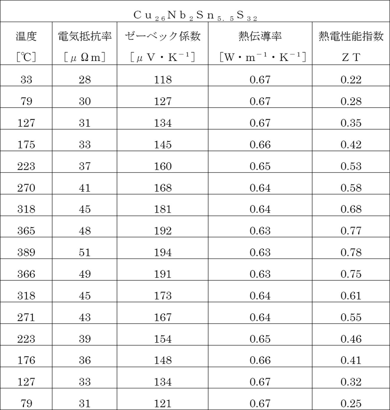

前掲表1に示すように、実施例1に係る熱電変換材料の熱電性能指数ZTは、365℃以上の温度環境下で特許文献1に記載のコルーサイトにおける最大の熱電性能指数ZT=0.73を超え、389℃の温度環境下において最大の0.78を示した。0.78との熱電性能指数ZTは、実施例1に係る熱電変換材料が現段階で世界最高レベルの性能を有することを示している。
また、前掲表1及び表2から確認されるように、前記化学式(1)中のAで示す金属材料をNbとし、かつ、Eで示す金属材料をSnとし、yで示す数値(欠損量)を0.5としてSn欠損を導入した実施例1に係る熱電変換材料では、Sn欠損を導入しないこと以外は、同様にして製造された比較例1に係る熱電変換材料と比べ、電気抵抗率ρが減少し、熱電性能指数ZTが増加していることが分かる。また、同等の温度条件下で比較したときのSn欠損の導入による熱電性能指数ZTの向上効果は、最大で0.26を記録し、実施例1に係る熱電変換材料では、比較例1に係る熱電変換材料と比べ、飛躍的な熱電性能指数ZTの向上が確認される。
また、Sn欠損を導入した実施例1に係る熱電変換材料の熱電性能指数ZTの値0.78は、同じくSn欠損を導入した非特許文献3におけるCu26V2Sn5.5S32の熱電性能指数ZTの値0.62と比べて30%程度高く、前記化学式(1)中のAで示される金属材料をVからNbに変更することで、熱電性能指数ZTの顕著な向上が確認される。
また、Sn欠損を導入したことに伴う実施例1に係る熱電変換材料の熱電性能指数ZTの向上効果(熱電性能指数ZTが0.26向上)は、Sn欠損を導入したことに伴う非特許文献3におけるCu26V2Sn5.5S32の熱電性能指数ZTの向上効果(熱電性能指数ZTが0.06向上)と比べて、4倍以上であり格段に大きい。
また、前掲表1及び表2から確認されるように、前記化学式(1)中のAで示す金属材料をNbとし、かつ、Eで示す金属材料をSnとし、yで示す数値(欠損量)を0.5としてSn欠損を導入した実施例1に係る熱電変換材料では、Sn欠損を導入しないこと以外は、同様にして製造された比較例1に係る熱電変換材料と比べ、電気抵抗率ρが減少し、熱電性能指数ZTが増加していることが分かる。また、同等の温度条件下で比較したときのSn欠損の導入による熱電性能指数ZTの向上効果は、最大で0.26を記録し、実施例1に係る熱電変換材料では、比較例1に係る熱電変換材料と比べ、飛躍的な熱電性能指数ZTの向上が確認される。
また、Sn欠損を導入した実施例1に係る熱電変換材料の熱電性能指数ZTの値0.78は、同じくSn欠損を導入した非特許文献3におけるCu26V2Sn5.5S32の熱電性能指数ZTの値0.62と比べて30%程度高く、前記化学式(1)中のAで示される金属材料をVからNbに変更することで、熱電性能指数ZTの顕著な向上が確認される。
また、Sn欠損を導入したことに伴う実施例1に係る熱電変換材料の熱電性能指数ZTの向上効果(熱電性能指数ZTが0.26向上)は、Sn欠損を導入したことに伴う非特許文献3におけるCu26V2Sn5.5S32の熱電性能指数ZTの向上効果(熱電性能指数ZTが0.06向上)と比べて、4倍以上であり格段に大きい。
(実施例2)
原料を、Cu(1.409g)、Nb(0.159g)、Sn(0.557g)、S(0.875g)からCu(1.4414g)、Ta(0.3163g)、Ge(0.3485g)、S(0.8932g)に変更し、組成がCu26Ta2Ge5.5S32の多結晶試料を得たこと以外は、実施例1と同様にして、実施例2に係る熱電変換材料を製造した。なお、得られた多結晶試料の生成相は、粉末X線回折により確認した。
原料を、Cu(1.409g)、Nb(0.159g)、Sn(0.557g)、S(0.875g)からCu(1.4414g)、Ta(0.3163g)、Ge(0.3485g)、S(0.8932g)に変更し、組成がCu26Ta2Ge5.5S32の多結晶試料を得たこと以外は、実施例1と同様にして、実施例2に係る熱電変換材料を製造した。なお、得られた多結晶試料の生成相は、粉末X線回折により確認した。
(比較例2)
原料を、Cu(1.4414g)、Ta(0.3163g)、Ge(0.3485g)、S(0.8932g)からCu(1.426g)、Ta(0.313g)、Ge(0.375g)、S(0.886g)に変更し、組成がCu26Ta2Ge6S32の多結晶試料を得たこと以外は、実施例2と同様にして、比較例2に係る熱電変換材料を製造した。なお、得られた多結晶試料の生成相は、粉末X線回折により確認した。
原料を、Cu(1.4414g)、Ta(0.3163g)、Ge(0.3485g)、S(0.8932g)からCu(1.426g)、Ta(0.313g)、Ge(0.375g)、S(0.886g)に変更し、組成がCu26Ta2Ge6S32の多結晶試料を得たこと以外は、実施例2と同様にして、比較例2に係る熱電変換材料を製造した。なお、得られた多結晶試料の生成相は、粉末X線回折により確認した。
実施例2に係る熱電変換材料に対し、実施例1に係る熱電変換材料と同様に測定を行ったゼーベック係数S、電気抵抗率ρ、及び熱伝導率κの各測定結果と、この測定結果から計算した熱電性能指数ZTとを下記表3に示す。
また、比較例2に係る熱電変換材料に対し、実施例1に係る熱電変換材料と同様に測定を行ったゼーベック係数S、電気抵抗率ρ、及び熱伝導率κの各測定結果と、この測定結果から計算した熱電性能指数ZTとを下記表4に示す。
また、比較例2に係る熱電変換材料に対し、実施例1に係る熱電変換材料と同様に測定を行ったゼーベック係数S、電気抵抗率ρ、及び熱伝導率κの各測定結果と、この測定結果から計算した熱電性能指数ZTとを下記表4に示す。
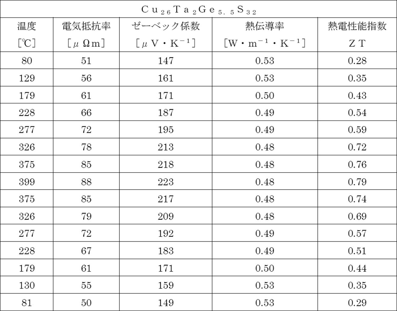
前掲表3に示すように、実施例2に係る熱電変換材料の熱電性能指数ZTは、特許文献1に記載のコルーサイトにおける最大の熱電性能指数ZT=0.73を超え、399℃の温度環境下において最大の0.79を示した。0.79との熱電性能指数ZTは、実施例3に係る熱電変換材料が現段階で世界最高レベルの性能を有することを示している。
また、前掲表3及び表4から確認されるように、前記化学式(1)中のAで示す金属材料をTaとし、かつ、Eで示す金属材料をGeとし、yで示す数値(欠損量)を0.5としてSn欠損を導入した実施例2に係る熱電変換材料では、Sn欠損を導入しないこと以外は、同様にして製造された比較例2に係る熱電変換材料と比べ、電気抵抗率ρが減少し、熱電性能指数ZTが増加していることが分かる。また、同等の温度条件下で比較したときのSn欠損の導入による熱電性能指数ZTの向上効果は、最大で0.13を記録し、実施例2に係る熱電変換材料では、比較例2に係る熱電変換材料と比べ、飛躍的な熱電性能指数ZTの向上が確認される。
また、Ge欠損を導入した実施例2に係る熱電変換材料の熱電性能指数ZTの値0.79は、Sn欠損を導入した非特許文献3におけるCu26V2Sn5.5S32の熱電性能指数ZTの値0.62と比べて30%程度高く、前記化学式(1)中のAで示される金属材料をVからNbに変更することで、熱電性能指数ZTの顕著な向上が確認される。
また、Ge欠損を導入したことに伴う実施例2に係る熱電変換材料の熱電性能指数ZTの向上効果(熱電性能指数ZTが0.13向上)は、Sn欠損を導入したことに伴う非特許文献3におけるCu26V2Sn5.5S32の熱電性能指数ZTの向上効果(熱電性能指数ZTが0.06向上)と比べて2倍以上であり、格段に大きい。
また、前掲表3及び表4から確認されるように、前記化学式(1)中のAで示す金属材料をTaとし、かつ、Eで示す金属材料をGeとし、yで示す数値(欠損量)を0.5としてSn欠損を導入した実施例2に係る熱電変換材料では、Sn欠損を導入しないこと以外は、同様にして製造された比較例2に係る熱電変換材料と比べ、電気抵抗率ρが減少し、熱電性能指数ZTが増加していることが分かる。また、同等の温度条件下で比較したときのSn欠損の導入による熱電性能指数ZTの向上効果は、最大で0.13を記録し、実施例2に係る熱電変換材料では、比較例2に係る熱電変換材料と比べ、飛躍的な熱電性能指数ZTの向上が確認される。
また、Ge欠損を導入した実施例2に係る熱電変換材料の熱電性能指数ZTの値0.79は、Sn欠損を導入した非特許文献3におけるCu26V2Sn5.5S32の熱電性能指数ZTの値0.62と比べて30%程度高く、前記化学式(1)中のAで示される金属材料をVからNbに変更することで、熱電性能指数ZTの顕著な向上が確認される。
また、Ge欠損を導入したことに伴う実施例2に係る熱電変換材料の熱電性能指数ZTの向上効果(熱電性能指数ZTが0.13向上)は、Sn欠損を導入したことに伴う非特許文献3におけるCu26V2Sn5.5S32の熱電性能指数ZTの向上効果(熱電性能指数ZTが0.06向上)と比べて2倍以上であり、格段に大きい。
(実施例3)
原料を、Cu(1.409g)、Nb(0.159g)、Sn(0.557g)、S(0.875g)からCu(1.3209g)、Ta(0.2898g)、Sn(0.5700g)、S(0.8213g)に変更し、組成がCu26Ta2Sn5.5S32の多結晶試料を得たこと以外は、実施例1と同様にして、実施例3に係る熱電変換材料を製造した。なお、得られた多結晶試料の生成相は、粉末X線回折により確認した。
原料を、Cu(1.409g)、Nb(0.159g)、Sn(0.557g)、S(0.875g)からCu(1.3209g)、Ta(0.2898g)、Sn(0.5700g)、S(0.8213g)に変更し、組成がCu26Ta2Sn5.5S32の多結晶試料を得たこと以外は、実施例1と同様にして、実施例3に係る熱電変換材料を製造した。なお、得られた多結晶試料の生成相は、粉末X線回折により確認した。
(比較例3)
原料を、Cu(1.3209g)、Ta(0.2898g)、Sn(0.5700g)、S(0.8213g)からCu(1.5638g)、Ta(0.343g)、Sn(0.6198g)、S(0.9725g)に変更し、組成がCu26Ta2Sn6S32の多結晶試料を得たこと以外は、実施例3と同様にして、比較例3に係る熱電変換材料を製造した。なお、得られた多結晶試料の生成相は、粉末X線回折により確認した。
原料を、Cu(1.3209g)、Ta(0.2898g)、Sn(0.5700g)、S(0.8213g)からCu(1.5638g)、Ta(0.343g)、Sn(0.6198g)、S(0.9725g)に変更し、組成がCu26Ta2Sn6S32の多結晶試料を得たこと以外は、実施例3と同様にして、比較例3に係る熱電変換材料を製造した。なお、得られた多結晶試料の生成相は、粉末X線回折により確認した。
実施例3に係る熱電変換材料に対し、実施例1に係る熱電変換材料と同様に測定を行ったゼーベック係数S、電気抵抗率ρ、及び熱伝導率κの各測定結果と、この測定結果から計算した熱電性能指数ZTとを下記表5に示す。
また、比較例3に係る熱電変換材料に対し、実施例1に係る熱電変換材料と同様に測定を行ったゼーベック係数S、電気抵抗率ρ、及び熱伝導率κの各測定結果と、この測定結果から計算した熱電性能指数ZTとを下記表6に示す。
また、比較例3に係る熱電変換材料に対し、実施例1に係る熱電変換材料と同様に測定を行ったゼーベック係数S、電気抵抗率ρ、及び熱伝導率κの各測定結果と、この測定結果から計算した熱電性能指数ZTとを下記表6に示す。


前掲表5に示すように、実施例3に係る熱電変換材料の熱電性能指数ZTは、特許文献1に記載のコルーサイトにおける最大の熱電性能指数ZT=0.73を超え、400℃の温度環境下において最大の0.97を示した。0.97との熱電性能指数ZTは、実施例3に係る熱電変換材料が現段階で世界最高レベルの性能を有することを示している。
また、前掲表5及び表6から確認されるように、前記化学式(1)中のAで示す金属材料をTaとし、かつ、Eで示す金属材料をSnとし、yで示す数値(欠損量)を0.5としてSn欠損を導入した実施例3に係る熱電変換材料では、Sn欠損を導入しないこと以外は、同様にして製造された比較例3に係る熱電変換材料と比べ、電気抵抗率ρが減少し、熱電性能指数ZTが増加していることが分かる。また、同等の温度条件下で比較したときのSn欠損の導入による熱電性能指数ZTの向上効果は、最大で0.19を記録し、実施例3に係る熱電変換材料では、比較例3に係る熱電変換材料と比べ、飛躍的な熱電性能指数ZTの向上が確認される。
また、Sn欠損を導入した実施例3に係る熱電変換材料の熱電性能指数ZTの値0.97は、Sn欠損を導入した非特許文献3におけるCu26V2Sn5.5S32の熱電性能指数ZTの値0.62と比べて50%程度高く、前記化学式(1)中のAで示される金属材料をVからTaに変更することで、熱電性能指数ZTの顕著な向上が確認される。
また、Sn欠損を導入したことに伴う実施例3に係る熱電変換材料の熱電性能指数ZTの向上効果(熱電性能指数ZTが0.19向上)は、Sn欠損を導入したことに伴う非特許文献3におけるCu26V2Sn5.5S32の熱電性能指数ZTの向上効果(熱電性能指数ZTが0.06向上)と比べて3倍以上であり、格段に大きい。
また、前掲表5及び表6から確認されるように、前記化学式(1)中のAで示す金属材料をTaとし、かつ、Eで示す金属材料をSnとし、yで示す数値(欠損量)を0.5としてSn欠損を導入した実施例3に係る熱電変換材料では、Sn欠損を導入しないこと以外は、同様にして製造された比較例3に係る熱電変換材料と比べ、電気抵抗率ρが減少し、熱電性能指数ZTが増加していることが分かる。また、同等の温度条件下で比較したときのSn欠損の導入による熱電性能指数ZTの向上効果は、最大で0.19を記録し、実施例3に係る熱電変換材料では、比較例3に係る熱電変換材料と比べ、飛躍的な熱電性能指数ZTの向上が確認される。
また、Sn欠損を導入した実施例3に係る熱電変換材料の熱電性能指数ZTの値0.97は、Sn欠損を導入した非特許文献3におけるCu26V2Sn5.5S32の熱電性能指数ZTの値0.62と比べて50%程度高く、前記化学式(1)中のAで示される金属材料をVからTaに変更することで、熱電性能指数ZTの顕著な向上が確認される。
また、Sn欠損を導入したことに伴う実施例3に係る熱電変換材料の熱電性能指数ZTの向上効果(熱電性能指数ZTが0.19向上)は、Sn欠損を導入したことに伴う非特許文献3におけるCu26V2Sn5.5S32の熱電性能指数ZTの向上効果(熱電性能指数ZTが0.06向上)と比べて3倍以上であり、格段に大きい。
(実施例4)
原料を、Cu(1.409g)、Nb(0.159g)、Sn(0.557g)、S(0.875g)からCu(1.5198g)、Nb(0.1718g)、Ge(0.3678g)、S(0.9438g)に変更し、組成がCu26Nb2Ge5.5S32の多結晶試料を得たこと以外は、実施例1と同様にして、実施例4に係る熱電変換材料を製造した。なお、得られた多結晶試料の生成相は、粉末X線回折により確認した。
原料を、Cu(1.409g)、Nb(0.159g)、Sn(0.557g)、S(0.875g)からCu(1.5198g)、Nb(0.1718g)、Ge(0.3678g)、S(0.9438g)に変更し、組成がCu26Nb2Ge5.5S32の多結晶試料を得たこと以外は、実施例1と同様にして、実施例4に係る熱電変換材料を製造した。なお、得られた多結晶試料の生成相は、粉末X線回折により確認した。
実施例4に係る熱電変換材料に対し、実施例1に係る熱電変換材料と同様に測定を行ったゼーベック係数S、電気抵抗率ρ、及び熱伝導率κの各測定結果と、この測定結果から計算した熱電性能指数ZTとを下記表7に示す。

前掲表7に示すように、実施例4に係る熱電変換材料の熱電性能指数ZTは、400℃の温度環境下において最大の0.73を示した。この値は、特許文献1に記載のコルーサイトにおける最大の熱電性能指数ZT=0.73に並ぶ値である。実施例4に係る熱電変換材料は、前記化学式(1)中のEで示される金属材料をSnからGeに変更したこと以外は、実施例1に係る熱電変換材料と同じ化合物であり、前記化学式(1)中のEで示される金属材料をGeに変更しても、高い熱電性能指数ZTを得られることが確認される。
また、Ge欠損を導入した実施例4に係る熱電変換材料の熱電性能指数ZTの値0.73は、Sn欠損を導入した非特許文献3におけるCu26V2Sn5.5S32の熱電性能指数ZTの値0.62と比べて20%程度高く、前記化学式(1)中のAで示される金属材料をVからNbに変更することで、熱電性能指数ZTの顕著な向上が確認される。
また、Ge欠損を導入した実施例4に係る熱電変換材料の熱電性能指数ZTの値0.73は、Sn欠損を導入した非特許文献3におけるCu26V2Sn5.5S32の熱電性能指数ZTの値0.62と比べて20%程度高く、前記化学式(1)中のAで示される金属材料をVからNbに変更することで、熱電性能指数ZTの顕著な向上が確認される。
(参考例)
非特許文献3によると、Cu26V2Sn5.5S32とCu26V2Sn6S32の焼結体の熱電性能指数は、それぞれCu26V2Sn5.5S32では387℃で0.62であり、Cu26V2Sn6S32では391℃で0.56であり、Cu26V2Sn6S32に対してSn欠損を導入したことによる熱電性能指数ZT向上の効果は、0.06程度である。即ち、前記化学式(1)中のAで示される金属材料をVとするコルーサイトにおいては、Sn欠損による熱電性能指数ZTの顕著な向上が認められない。
非特許文献3によると、Cu26V2Sn5.5S32とCu26V2Sn6S32の焼結体の熱電性能指数は、それぞれCu26V2Sn5.5S32では387℃で0.62であり、Cu26V2Sn6S32では391℃で0.56であり、Cu26V2Sn6S32に対してSn欠損を導入したことによる熱電性能指数ZT向上の効果は、0.06程度である。即ち、前記化学式(1)中のAで示される金属材料をVとするコルーサイトにおいては、Sn欠損による熱電性能指数ZTの顕著な向上が認められない。
前述の通り、前記化学式(1)中のAで示される金属材料が、V、Nb及びTaのいずれであっても、コルーサイト全体の価数に変わりはないため、いずれの金属材料を選択しても熱電性能指数ZTが等しくなることが予想される。しかし、Vを選択した非特許文献3に記載のコルーサイトよりも、Nb及びTaのいずれかを選択した実施例1~4に係る各熱電変換材料の方が数段大きな熱電性能指数ZTを示し、更には、過去に報告されたもののうち最も高い熱電性能指数ZTの報告例に係る特許文献1に記載の熱電変換材料よりも、実施例1~3に係る各熱電変換材料の方が大きな熱電変換性能指数ZTを得られており、本発明に係る前記熱電変換材料は、先の予想に反して、優れた熱電性能指数ZTを有する。
1,11,11’ 熱電変換材料層
2a,2b,12a,12b,12a’,12b’ 電極層
10 熱電変換素子
20 P型熱電変換素子
30 N型熱電変換素子
13 上部接合電極
14,14’ 下部接合電極
100 熱電変換モジュール
2a,2b,12a,12b,12a’,12b’ 電極層
10 熱電変換素子
20 P型熱電変換素子
30 N型熱電変換素子
13 上部接合電極
14,14’ 下部接合電極
100 熱電変換モジュール
Claims (6)
- 下記化学式(1)で表される化合物であることを特徴とする熱電変換材料。

- 化学式(1)中のxで示す数値が、0である請求項1に記載の熱電変換材料。
- 化学式(1)中のyで示す数値が、0より大きく0.5以下である請求項1から請求項2のいずれかに記載の熱電変換材料。
- 化学式(1)中のEで示す金属材料が、Sn及びGeの少なくともいずれかを含む請求項1から請求項3のいずれかに記載の熱電変換材料。
- 熱電性能指数ZTが、365℃~400℃の温度環境下において、0.73より大きい値を示す請求項1から請求項4のいずれかに記載の熱電変換材料。
- 請求項1から請求項5のいずれかに記載の熱電変換材料で形成される熱電変換材料層を有することを特徴とする熱電変換モジュール。
Priority Applications (1)
| Application Number | Priority Date | Filing Date | Title |
|---|---|---|---|
| US16/308,748 US11527692B2 (en) | 2016-06-10 | 2017-05-25 | Thermoelectric conversion material and thermoelectric conversion module |
Applications Claiming Priority (2)
| Application Number | Priority Date | Filing Date | Title |
|---|---|---|---|
| JP2016115935A JP6847410B2 (ja) | 2016-06-10 | 2016-06-10 | 熱電変換材料及び熱電変換モジュール |
| JP2016-115935 | 2016-06-10 |
Publications (1)
| Publication Number | Publication Date |
|---|---|
| WO2017212926A1 true WO2017212926A1 (ja) | 2017-12-14 |
Family
ID=60577830
Family Applications (1)
| Application Number | Title | Priority Date | Filing Date |
|---|---|---|---|
| PCT/JP2017/019482 Ceased WO2017212926A1 (ja) | 2016-06-10 | 2017-05-25 | 熱電変換材料及び熱電変換モジュール |
Country Status (3)
| Country | Link |
|---|---|
| US (1) | US11527692B2 (ja) |
| JP (1) | JP6847410B2 (ja) |
| WO (1) | WO2017212926A1 (ja) |
Families Citing this family (1)
| Publication number | Priority date | Publication date | Assignee | Title |
|---|---|---|---|---|
| JP6718800B2 (ja) * | 2016-11-28 | 2020-07-08 | 株式会社日本触媒 | 硫化物、半導体材料、及び熱電変換材料 |
Citations (1)
| Publication number | Priority date | Publication date | Assignee | Title |
|---|---|---|---|---|
| JP2016039372A (ja) * | 2014-08-05 | 2016-03-22 | 国立大学法人広島大学 | 熱電変換材料、およびそれを用いた熱電発電素子、ペルチェ冷却用素子 |
Family Cites Families (1)
| Publication number | Priority date | Publication date | Assignee | Title |
|---|---|---|---|---|
| CN104703947B (zh) * | 2012-07-06 | 2019-05-07 | 密歇根州立大学董事会 | 基于黝铜矿结构的用于热电设备的热电材料 |
-
2016
- 2016-06-10 JP JP2016115935A patent/JP6847410B2/ja active Active
-
2017
- 2017-05-25 US US16/308,748 patent/US11527692B2/en active Active
- 2017-05-25 WO PCT/JP2017/019482 patent/WO2017212926A1/ja not_active Ceased
Patent Citations (1)
| Publication number | Priority date | Publication date | Assignee | Title |
|---|---|---|---|---|
| JP2016039372A (ja) * | 2014-08-05 | 2016-03-22 | 国立大学法人広島大学 | 熱電変換材料、およびそれを用いた熱電発電素子、ペルチェ冷却用素子 |
Non-Patent Citations (1)
| Title |
|---|
| KIM, F. S. ET AL.: "Tuning the charge carrier density in the thermoelectric colusite", JOURNAL OF APPLIED PHYSICS, vol. 119, 4 May 2016 (2016-05-04), pages 175105 - 1 - 175105-5, XP012207370 * |
Also Published As
| Publication number | Publication date |
|---|---|
| US11527692B2 (en) | 2022-12-13 |
| JP2017220625A (ja) | 2017-12-14 |
| JP6847410B2 (ja) | 2021-03-24 |
| US20190148613A1 (en) | 2019-05-16 |
Similar Documents
| Publication | Publication Date | Title |
|---|---|---|
| Tan et al. | Thermoelectric power generation: from new materials to devices | |
| Ren et al. | Advanced thermoelectrics: materials, contacts, devices, and systems | |
| JP6164627B2 (ja) | 新規な化合物半導体及びその活用 | |
| KR102067647B1 (ko) | 열전소자의 제조방법 및 이를 이용한 열전냉각모듈 | |
| JP2013016685A (ja) | 熱電変換材料、熱電変換素子およびその作製方法 | |
| Jood et al. | Temperature-dependent structural variation and Cu substitution in thermoelectric silver selenide | |
| CN107534078B (zh) | 热电转换材料 | |
| JP6460225B2 (ja) | 熱電変換材料およびその製造方法 | |
| Pavan Kumar et al. | A new wide band gap thermoelectric quaternary selenide Cu2MgSnSe4 | |
| CN110218888B (zh) | 一种新型Zintl相热电材料及其制备方法 | |
| Chetty et al. | Thermoelectric properties of indium doped Cu2CdSnSe4 | |
| JP6256895B2 (ja) | 新規な化合物半導体及びその活用 | |
| JP6593870B2 (ja) | 熱電変換材料、およびそれを用いた熱電発電素子、ペルチェ冷却用素子 | |
| Chen et al. | Strategy of extra zr doping on the enhancement of thermoelectric performance for TiZr x NiSn synthesized by a modified solid-state reaction | |
| JPWO2014155591A1 (ja) | 高効率熱電変換ユニット | |
| JP6847410B2 (ja) | 熱電変換材料及び熱電変換モジュール | |
| KR102049009B1 (ko) | 신규한 화합물 반도체 및 그 활용 | |
| WO2014167801A1 (ja) | 熱電変換材料の製造方法 | |
| JP6617840B2 (ja) | p型熱電変換材料、熱電変換モジュール及びp型熱電変換材料の製造方法 | |
| Chen et al. | Enhancing Thermoelectric Performance of n-Type Bi2Te2. 7Se0. 3 through Incorporation of Amorphous Si3N4 Nanoparticles | |
| JP2009040649A (ja) | クラスレート化合物及びそれを用いた熱電変換素子 | |
| JP2008227321A (ja) | 熱電変換材料及びこれを用いた熱電変換モジュール | |
| WO2015121932A1 (ja) | 熱電変換材料およびそれを用いた熱電変換モジュール | |
| WO2016030964A1 (ja) | n型熱電変換材料及び熱電変換素子 | |
| JP2021044424A (ja) | 熱電変換材料 |
Legal Events
| Date | Code | Title | Description |
|---|---|---|---|
| 121 | Ep: the epo has been informed by wipo that ep was designated in this application |
Ref document number: 17810106 Country of ref document: EP Kind code of ref document: A1 |
|
| NENP | Non-entry into the national phase |
Ref country code: DE |
|
| 122 | Ep: pct application non-entry in european phase |
Ref document number: 17810106 Country of ref document: EP Kind code of ref document: A1 |