WO2017203775A1 - 薄膜形成用原料及び薄膜の製造方法 - Google Patents
薄膜形成用原料及び薄膜の製造方法 Download PDFInfo
- Publication number
- WO2017203775A1 WO2017203775A1 PCT/JP2017/007483 JP2017007483W WO2017203775A1 WO 2017203775 A1 WO2017203775 A1 WO 2017203775A1 JP 2017007483 W JP2017007483 W JP 2017007483W WO 2017203775 A1 WO2017203775 A1 WO 2017203775A1
- Authority
- WO
- WIPO (PCT)
- Prior art keywords
- thin film
- raw material
- forming
- carbon atoms
- zirconium
- Prior art date
- Legal status (The legal status is an assumption and is not a legal conclusion. Google has not performed a legal analysis and makes no representation as to the accuracy of the status listed.)
- Ceased
Links
Images


Classifications
-
- C—CHEMISTRY; METALLURGY
- C23—COATING METALLIC MATERIAL; COATING MATERIAL WITH METALLIC MATERIAL; CHEMICAL SURFACE TREATMENT; DIFFUSION TREATMENT OF METALLIC MATERIAL; COATING BY VACUUM EVAPORATION, BY SPUTTERING, BY ION IMPLANTATION OR BY CHEMICAL VAPOUR DEPOSITION, IN GENERAL; INHIBITING CORROSION OF METALLIC MATERIAL OR INCRUSTATION IN GENERAL
- C23C—COATING METALLIC MATERIAL; COATING MATERIAL WITH METALLIC MATERIAL; SURFACE TREATMENT OF METALLIC MATERIAL BY DIFFUSION INTO THE SURFACE, BY CHEMICAL CONVERSION OR SUBSTITUTION; COATING BY VACUUM EVAPORATION, BY SPUTTERING, BY ION IMPLANTATION OR BY CHEMICAL VAPOUR DEPOSITION, IN GENERAL
- C23C16/00—Chemical coating by decomposition of gaseous compounds, without leaving reaction products of surface material in the coating, i.e. chemical vapour deposition [CVD] processes
- C23C16/04—Coating on selected surface areas, e.g. using masks
- C23C16/045—Coating cavities or hollow spaces, e.g. interior of tubes; Infiltration of porous substrates
-
- C—CHEMISTRY; METALLURGY
- C07—ORGANIC CHEMISTRY
- C07F—ACYCLIC, CARBOCYCLIC OR HETEROCYCLIC COMPOUNDS CONTAINING ELEMENTS OTHER THAN CARBON, HYDROGEN, HALOGEN, OXYGEN, NITROGEN, SULFUR, SELENIUM OR TELLURIUM
- C07F7/00—Compounds containing elements of Groups 4 or 14 of the Periodic Table
-
- C—CHEMISTRY; METALLURGY
- C07—ORGANIC CHEMISTRY
- C07F—ACYCLIC, CARBOCYCLIC OR HETEROCYCLIC COMPOUNDS CONTAINING ELEMENTS OTHER THAN CARBON, HYDROGEN, HALOGEN, OXYGEN, NITROGEN, SULFUR, SELENIUM OR TELLURIUM
- C07F7/00—Compounds containing elements of Groups 4 or 14 of the Periodic Table
- C07F7/28—Titanium compounds
-
- C—CHEMISTRY; METALLURGY
- C23—COATING METALLIC MATERIAL; COATING MATERIAL WITH METALLIC MATERIAL; CHEMICAL SURFACE TREATMENT; DIFFUSION TREATMENT OF METALLIC MATERIAL; COATING BY VACUUM EVAPORATION, BY SPUTTERING, BY ION IMPLANTATION OR BY CHEMICAL VAPOUR DEPOSITION, IN GENERAL; INHIBITING CORROSION OF METALLIC MATERIAL OR INCRUSTATION IN GENERAL
- C23C—COATING METALLIC MATERIAL; COATING MATERIAL WITH METALLIC MATERIAL; SURFACE TREATMENT OF METALLIC MATERIAL BY DIFFUSION INTO THE SURFACE, BY CHEMICAL CONVERSION OR SUBSTITUTION; COATING BY VACUUM EVAPORATION, BY SPUTTERING, BY ION IMPLANTATION OR BY CHEMICAL VAPOUR DEPOSITION, IN GENERAL
- C23C16/00—Chemical coating by decomposition of gaseous compounds, without leaving reaction products of surface material in the coating, i.e. chemical vapour deposition [CVD] processes
- C23C16/06—Chemical coating by decomposition of gaseous compounds, without leaving reaction products of surface material in the coating, i.e. chemical vapour deposition [CVD] processes characterised by the deposition of metallic material
- C23C16/18—Chemical coating by decomposition of gaseous compounds, without leaving reaction products of surface material in the coating, i.e. chemical vapour deposition [CVD] processes characterised by the deposition of metallic material from metallo-organic compounds
-
- C—CHEMISTRY; METALLURGY
- C23—COATING METALLIC MATERIAL; COATING MATERIAL WITH METALLIC MATERIAL; CHEMICAL SURFACE TREATMENT; DIFFUSION TREATMENT OF METALLIC MATERIAL; COATING BY VACUUM EVAPORATION, BY SPUTTERING, BY ION IMPLANTATION OR BY CHEMICAL VAPOUR DEPOSITION, IN GENERAL; INHIBITING CORROSION OF METALLIC MATERIAL OR INCRUSTATION IN GENERAL
- C23C—COATING METALLIC MATERIAL; COATING MATERIAL WITH METALLIC MATERIAL; SURFACE TREATMENT OF METALLIC MATERIAL BY DIFFUSION INTO THE SURFACE, BY CHEMICAL CONVERSION OR SUBSTITUTION; COATING BY VACUUM EVAPORATION, BY SPUTTERING, BY ION IMPLANTATION OR BY CHEMICAL VAPOUR DEPOSITION, IN GENERAL
- C23C16/00—Chemical coating by decomposition of gaseous compounds, without leaving reaction products of surface material in the coating, i.e. chemical vapour deposition [CVD] processes
- C23C16/22—Chemical coating by decomposition of gaseous compounds, without leaving reaction products of surface material in the coating, i.e. chemical vapour deposition [CVD] processes characterised by the deposition of inorganic material, other than metallic material
- C23C16/30—Deposition of compounds, mixtures or solid solutions, e.g. borides, carbides, nitrides
- C23C16/40—Oxides
-
- C—CHEMISTRY; METALLURGY
- C23—COATING METALLIC MATERIAL; COATING MATERIAL WITH METALLIC MATERIAL; CHEMICAL SURFACE TREATMENT; DIFFUSION TREATMENT OF METALLIC MATERIAL; COATING BY VACUUM EVAPORATION, BY SPUTTERING, BY ION IMPLANTATION OR BY CHEMICAL VAPOUR DEPOSITION, IN GENERAL; INHIBITING CORROSION OF METALLIC MATERIAL OR INCRUSTATION IN GENERAL
- C23C—COATING METALLIC MATERIAL; COATING MATERIAL WITH METALLIC MATERIAL; SURFACE TREATMENT OF METALLIC MATERIAL BY DIFFUSION INTO THE SURFACE, BY CHEMICAL CONVERSION OR SUBSTITUTION; COATING BY VACUUM EVAPORATION, BY SPUTTERING, BY ION IMPLANTATION OR BY CHEMICAL VAPOUR DEPOSITION, IN GENERAL
- C23C16/00—Chemical coating by decomposition of gaseous compounds, without leaving reaction products of surface material in the coating, i.e. chemical vapour deposition [CVD] processes
- C23C16/22—Chemical coating by decomposition of gaseous compounds, without leaving reaction products of surface material in the coating, i.e. chemical vapour deposition [CVD] processes characterised by the deposition of inorganic material, other than metallic material
- C23C16/30—Deposition of compounds, mixtures or solid solutions, e.g. borides, carbides, nitrides
- C23C16/40—Oxides
- C23C16/405—Oxides of refractory metals or yttrium
-
- C—CHEMISTRY; METALLURGY
- C23—COATING METALLIC MATERIAL; COATING MATERIAL WITH METALLIC MATERIAL; CHEMICAL SURFACE TREATMENT; DIFFUSION TREATMENT OF METALLIC MATERIAL; COATING BY VACUUM EVAPORATION, BY SPUTTERING, BY ION IMPLANTATION OR BY CHEMICAL VAPOUR DEPOSITION, IN GENERAL; INHIBITING CORROSION OF METALLIC MATERIAL OR INCRUSTATION IN GENERAL
- C23C—COATING METALLIC MATERIAL; COATING MATERIAL WITH METALLIC MATERIAL; SURFACE TREATMENT OF METALLIC MATERIAL BY DIFFUSION INTO THE SURFACE, BY CHEMICAL CONVERSION OR SUBSTITUTION; COATING BY VACUUM EVAPORATION, BY SPUTTERING, BY ION IMPLANTATION OR BY CHEMICAL VAPOUR DEPOSITION, IN GENERAL
- C23C16/00—Chemical coating by decomposition of gaseous compounds, without leaving reaction products of surface material in the coating, i.e. chemical vapour deposition [CVD] processes
- C23C16/44—Chemical coating by decomposition of gaseous compounds, without leaving reaction products of surface material in the coating, i.e. chemical vapour deposition [CVD] processes characterised by the method of coating
- C23C16/455—Chemical coating by decomposition of gaseous compounds, without leaving reaction products of surface material in the coating, i.e. chemical vapour deposition [CVD] processes characterised by the method of coating characterised by the method used for introducing gases into reaction chamber or for modifying gas flows in reaction chamber
- C23C16/45523—Pulsed gas flow or change of composition over time
- C23C16/45525—Atomic layer deposition [ALD]
- C23C16/45553—Atomic layer deposition [ALD] characterized by the use of precursors specially adapted for ALD
-
- H—ELECTRICITY
- H10—SEMICONDUCTOR DEVICES; ELECTRIC SOLID-STATE DEVICES NOT OTHERWISE PROVIDED FOR
- H10P—GENERIC PROCESSES OR APPARATUS FOR THE MANUFACTURE OR TREATMENT OF DEVICES COVERED BY CLASS H10
- H10P14/00—Formation of materials, e.g. in the shape of layers or pillars
- H10P14/40—Formation of materials, e.g. in the shape of layers or pillars of conductive or resistive materials
- H10P14/42—Formation of materials, e.g. in the shape of layers or pillars of conductive or resistive materials using a gas or vapour
- H10P14/43—Chemical deposition, e.g. chemical vapour deposition [CVD]
-
- H—ELECTRICITY
- H10—SEMICONDUCTOR DEVICES; ELECTRIC SOLID-STATE DEVICES NOT OTHERWISE PROVIDED FOR
- H10P—GENERIC PROCESSES OR APPARATUS FOR THE MANUFACTURE OR TREATMENT OF DEVICES COVERED BY CLASS H10
- H10P14/00—Formation of materials, e.g. in the shape of layers or pillars
- H10P14/60—Formation of materials, e.g. in the shape of layers or pillars of insulating materials
- H10P14/69—Inorganic materials
- H10P14/692—Inorganic materials composed of oxides, glassy oxides or oxide-based glasses
- H10P14/6938—Inorganic materials composed of oxides, glassy oxides or oxide-based glasses the material containing at least one metal element, e.g. metal oxides, metal oxynitrides or metal oxycarbides
- H10P14/6939—Inorganic materials composed of oxides, glassy oxides or oxide-based glasses the material containing at least one metal element, e.g. metal oxides, metal oxynitrides or metal oxycarbides characterised by the metal
- H10P14/69392—Inorganic materials composed of oxides, glassy oxides or oxide-based glasses the material containing at least one metal element, e.g. metal oxides, metal oxynitrides or metal oxycarbides characterised by the metal the material containing hafnium, e.g. HfO2
-
- H—ELECTRICITY
- H10—SEMICONDUCTOR DEVICES; ELECTRIC SOLID-STATE DEVICES NOT OTHERWISE PROVIDED FOR
- H10P—GENERIC PROCESSES OR APPARATUS FOR THE MANUFACTURE OR TREATMENT OF DEVICES COVERED BY CLASS H10
- H10P14/00—Formation of materials, e.g. in the shape of layers or pillars
- H10P14/60—Formation of materials, e.g. in the shape of layers or pillars of insulating materials
- H10P14/69—Inorganic materials
- H10P14/692—Inorganic materials composed of oxides, glassy oxides or oxide-based glasses
- H10P14/6938—Inorganic materials composed of oxides, glassy oxides or oxide-based glasses the material containing at least one metal element, e.g. metal oxides, metal oxynitrides or metal oxycarbides
- H10P14/6939—Inorganic materials composed of oxides, glassy oxides or oxide-based glasses the material containing at least one metal element, e.g. metal oxides, metal oxynitrides or metal oxycarbides characterised by the metal
- H10P14/69394—Inorganic materials composed of oxides, glassy oxides or oxide-based glasses the material containing at least one metal element, e.g. metal oxides, metal oxynitrides or metal oxycarbides characterised by the metal the material containing titanium, e.g. TiO2
-
- H—ELECTRICITY
- H10—SEMICONDUCTOR DEVICES; ELECTRIC SOLID-STATE DEVICES NOT OTHERWISE PROVIDED FOR
- H10P—GENERIC PROCESSES OR APPARATUS FOR THE MANUFACTURE OR TREATMENT OF DEVICES COVERED BY CLASS H10
- H10P14/00—Formation of materials, e.g. in the shape of layers or pillars
- H10P14/60—Formation of materials, e.g. in the shape of layers or pillars of insulating materials
- H10P14/69—Inorganic materials
- H10P14/692—Inorganic materials composed of oxides, glassy oxides or oxide-based glasses
- H10P14/6938—Inorganic materials composed of oxides, glassy oxides or oxide-based glasses the material containing at least one metal element, e.g. metal oxides, metal oxynitrides or metal oxycarbides
- H10P14/6939—Inorganic materials composed of oxides, glassy oxides or oxide-based glasses the material containing at least one metal element, e.g. metal oxides, metal oxynitrides or metal oxycarbides characterised by the metal
- H10P14/69395—Inorganic materials composed of oxides, glassy oxides or oxide-based glasses the material containing at least one metal element, e.g. metal oxides, metal oxynitrides or metal oxycarbides characterised by the metal the material containing zirconium, e.g. ZrO2
Definitions
- the present invention relates to a raw material for forming a thin film containing a specific compound and a method for producing a thin film using the raw material for forming a thin film.
- Thin film materials containing titanium, zirconium or hafnium are applied to applications such as semiconductors, photovoltaic cells and TFTs, and are mainly used as high dielectric materials for semiconductor materials.
- Examples of the method for producing the thin film include a sputtering method, an ion plating method, a MOD method such as a coating pyrolysis method and a sol-gel method, a chemical vapor deposition method, etc., but has excellent composition controllability and step coverage. Since it has many advantages such as being suitable for mass production and being capable of hybrid integration, chemical vapor deposition (hereinafter sometimes simply referred to as CVD) method including ALD (Atomic Layer Deposition) method Is the optimal manufacturing process.
- CVD chemical vapor deposition
- ALD Atomic Layer Deposition
- Patent Document 1 discloses that a specific zirconium complex is used as a material that can be used in a CVD method or an ALD method.
- Patent Document 2 discloses that a specific metal complex is used as a material that can be used in a CVD method or an ALD method.
- Patent Document 1 and Patent Document 2 do not specifically describe the thin film forming raw material of the present invention.
- a thin film forming raw material capable of forming a thin film uniformly in a groove having an aspect ratio of about 10 to 200 is required.
- the present invention provides a raw material for forming a thin film comprising a compound represented by the following general formula (1).
- R 1 represents a linear or branched alkyl group having 2 to 4 carbon atoms
- R 2 to R 5 each independently represents a linear or branched alkyl group having 1 to 4 carbon atoms.
- A represents an alkanediyl group having 1 to 4 carbon atoms
- M represents titanium, zirconium or hafnium, provided that when M is zirconium, A is an alkanediyl group having 3 or 4 carbon atoms. .
- the present invention introduces a vapor containing a compound represented by the general formula (1) obtained by vaporizing the raw material for forming a thin film into a film forming chamber provided with a substrate, and decomposes the compound. And / or a method for producing a thin film, which is chemically reacted to form a thin film containing at least one atom selected from titanium, zirconium and hafnium on the surface of the substrate.
- the present invention it is possible to obtain a thin film forming raw material that can form a high quality thin film uniformly in a groove having high thermal stability and an aspect ratio of about 10 to 200.
- the raw material for forming a thin film of the present invention is suitable as a raw material for forming a metal thin film by a CVD method. Since the thin film forming raw material of the present invention is applicable to the ALD method, it is particularly suitable as a thin film forming raw material for the ALD method that exhibits the above effects.
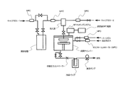
- FIG. 1 is a schematic view showing an example of an apparatus for chemical vapor deposition used in the method for producing a thin film according to the present invention.
- FIG. 2 is a schematic diagram showing another example of a chemical vapor deposition apparatus used in the thin film manufacturing method according to the present invention.
- FIG. 3 is a schematic view showing another example of the chemical vapor deposition apparatus used in the method for producing a thin film according to the present invention.
- FIG. 4 is a schematic diagram showing another example of a chemical vapor deposition apparatus used in the thin film manufacturing method according to the present invention.
- the raw material for forming a thin film of the present invention contains the compound represented by the general formula (1) and is suitable as a precursor for a thin film production method having a vaporization step such as a CVD method. It can also be used to form a thin film.
- R 1 represents a linear or branched alkyl group having 2 to 4 carbon atoms
- R 2 to R 5 are each independently a linear or branched group having 1 to 4 carbon atoms.
- A represents an alkanediyl group having 1 to 4 carbon atoms
- M represents titanium, zirconium or hafnium. However, when M is zirconium, A is an alkanediyl group having 3 or 4 carbon atoms.
- Examples of the linear or branched alkyl group having 2 to 4 carbon atoms represented by R 1 include ethyl, propyl, isopropyl, butyl, isobutyl, sec-butyl and tert-butyl.
- Examples of the linear or branched alkyl group having 1 to 4 carbon atoms represented by R 2 to R 5 include methyl, ethyl, propyl, isopropyl, butyl, isobutyl, sec-butyl, tert-butyl, etc. Is mentioned.
- alkanediyl group having 1 to 4 carbon atoms represented by A examples include methylene, ethylene, propane-1,3-diyl, propane-1,2-diyl, butane-1,4-diyl, butane-1 , 3-diyl and the like.
- alkanediyl group having 3 or 4 carbon atoms represented by A examples include propane-1,3-diyl, propane-1,2-diyl, butane-1,4-diyl, butane-1,3-diyl. Etc.
- R 1 is any one of ethyl, isopropyl, sec-butyl and tert-butyl
- R 2 to R 5 are preferably a methyl group because the vapor pressure is high.
- R 1 to R 5 and A can be appropriately selected depending on the solubility in the solvent used, the thin film formation reaction, and the like.
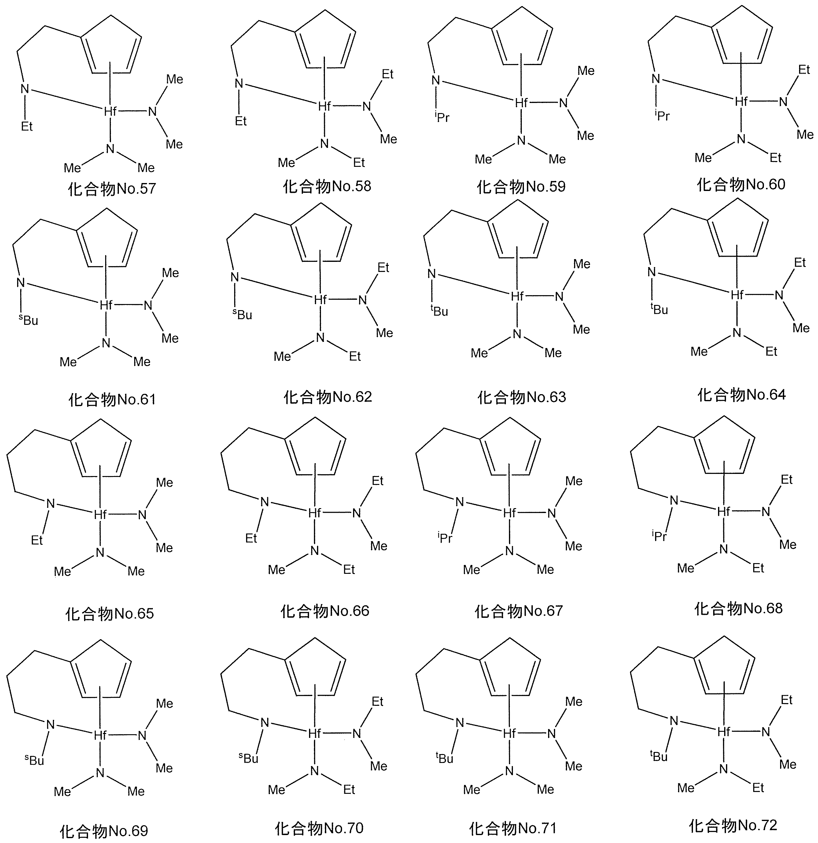
- the compound represented by the general formula (1) include, for example, the following chemical formula No. 1-No.
- the compound represented by 88 is mentioned.
- the following chemical formula No. 1-No. 88 “Me” represents a methyl group, “Et” represents an ethyl group, “ i Pr” represents an isopropyl group, “ s Bu” represents a secondary butyl group, and “ t Bu” represents tert-butyl. Represents a group.
- the compound represented by the general formula (1) contained in the thin film forming raw material of the present invention is not particularly limited by the production method, and is produced by applying a known reaction.
- M is titanium
- an alkylaminoalkylcyclopentadiene compound having a corresponding structure may be reacted with tetrakis (dialkylamino) titanium under a temperature condition of 10 to 50 ° C. in a solvent such as toluene.
- M is zirconium
- tetrakis (dialkylamino) zirconium in a solvent such as toluene may be reacted with an alkylaminoalkylcyclopentadiene compound having a corresponding structure at a temperature of 10 to 50 ° C.
- tetrakis (dialkylamino) hafnium may be reacted with an alkylaminoalkylcyclopentadiene compound having a corresponding structure at a temperature of 10 to 50 ° C. in a solvent such as toluene.
- the form of the thin film forming raw material of the present invention varies depending on the manufacturing process to which the thin film forming raw material is applied.
- the raw material for forming a thin film of the present invention is a metal compound or a semi-metallic compound other than the compound represented by the general formula (1) Is not contained.
- the raw material contains a compound (hereinafter also referred to as other precursor) containing a metal other than the metal selected from the group consisting of titanium, zirconium and hafnium and / or a semimetal.
- the thin film forming raw material of the present invention may further contain an organic solvent and / or a nucleophilic reagent. Since the raw material for forming a thin film of the present invention is suitable for the CVD method and the ALD method as described above, it is particularly useful as a raw material for chemical vapor deposition (hereinafter sometimes referred to as a CVD raw material).
- the raw material for forming a thin film of the present invention is a raw material for chemical vapor deposition
- the form is appropriately selected depending on the method such as the transport and supply method of the CVD method used.
- the raw material for CVD is vaporized by heating and / or depressurizing in a container in which the raw material is stored (hereinafter sometimes simply referred to as a raw material container), and is necessary.
- a carrier gas such as argon, nitrogen, helium or the like
- the compound itself represented by the general formula (1) can be used as a raw material for CVD.
- the compound itself represented by the general formula (1) or a solution obtained by dissolving the compound in an organic solvent can be used as a CVD raw material.
- These CVD raw materials may further contain other precursors, nucleophilic reagents, and the like.
- the CVD raw material is vaporized and supplied independently for each component (hereinafter sometimes referred to as a single source method), and the multi-component raw material is mixed in advance with a desired composition.
- a method of vaporizing and supplying a mixed raw material hereinafter, sometimes referred to as a cocktail sauce method.
- the raw material for forming a thin film of the present invention uses a mixture of the compound represented by the general formula (1) and another precursor or a mixed solution obtained by dissolving the mixture in an organic solvent as a CVD raw material. be able to.
- This mixture or mixed solution may further contain a nucleophilic reagent and the like.
- the organic solvent is not particularly limited and a known general organic solvent can be used.
- the organic solvent include acetates such as ethyl acetate, butyl acetate and methoxyethyl acetate; ethers such as tetrahydrofuran, tetrahydropyran, ethylene glycol dimethyl ether, diethylene glycol dimethyl ether, triethylene glycol dimethyl ether, dibutyl ether and dioxane; Ketones such as butyl ketone, methyl isobutyl ketone, ethyl butyl ketone, dipropyl ketone, diisobutyl ketone, methyl amyl ketone, cyclohexanone, methylcyclohexanone; hexane, cyclohexane, methylcyclohexane, dimethylcyclohexane, ethylcyclohexane, heptane, octan
- organic solvents may be used alone or in combination of two or more depending on the solubility of the solute, the relationship between the use temperature and boiling point, the flash point, and the like.
- the total amount of the precursor in the CVD raw material which is a solution obtained by dissolving the precursor in the organic solvent, is 0.01 to 2.0 mol / liter, particularly 0.05 to 1.0 mol / liter. It is preferable to make it liter.
- the amount of the entire precursor is represented by the general formula (1) when the raw material for forming a thin film of the present invention does not contain a metal compound and a metalloid compound other than the compound represented by the general formula (1).
- the amount of the compound, and the thin film forming raw material of the present invention contains a compound containing another metal and / or a compound containing a metalloid (another precursor) in addition to the compound represented by the general formula (1). In this case, the total amount of the compound represented by the general formula (1) and other precursors.
- the other precursor used together with the thin film forming raw material of the present invention is not particularly limited, and a well-known general precursor used for the CVD raw material may be used. it can.
- hydrides hydroxides, halides, azides, alkyls, alkenyls, cycloalkyls, aryls, alkynyls, aminos, dialkylaminoalkyls, monoalkylaminos, dialkylaminos, diamines, di (silyls) -Alkyl) amino, di (alkyl-silyl) amino, disilylamino, alkoxy, alkoxyalkyl, hydrazide, phosphide, nitrile, dialkylaminoalkoxy, alkoxyalkyldialkylamino, siloxy, diketonate, cyclopentadienyl, silyl, pyrazolate, guanidinate, A group consisting of compounds having phosphoguanidinate, amidinate, phosphoamidinate, ketoiminate, diketiminate, carbonyl and phosphoamidinate as ligands Compounds of one kind or two kinds
- the precursor metal species include magnesium, calcium, strontium, barium, radium, scandium, yttrium, vanadium, niobium, tantalum, chromium, molybdenum, tungsten, manganese, iron, osmium, cobalt, rhodium, iridium, nickel, palladium, platinum , Copper, silver, gold, zinc, cadmium, aluminum, gallium, indium, germanium, tin, lead, antimony, bismuth, lanthanum, cerium, praseodymium, neodymium, samarium, europium, gadolinium, terbium, dysprosium, holmium, erbium, thulium Ytterbium.
- precursors described above are known in the art, and their manufacturing methods are also known.
- the inorganic salt of metal or its hydrate described above is reacted with the alkali metal alkoxide of the alcohol compound.
- a precursor can be manufactured.
- the metal inorganic salt or hydrate include metal halides and nitrates
- examples of the alkali metal alkoxide include sodium alkoxide, lithium alkoxide, and potassium alkoxide.
- the other precursor is preferably a compound that is similar to the compound represented by the general formula (1) in the behavior of heat and / or oxidative decomposition, and in the case of the cocktail source method, In addition to the similar behavior of heat and / or oxidative decomposition, those that do not undergo alteration due to chemical reaction or the like during mixing are preferred.
- Examples of other precursors described above include precursors containing rare earth elements.
- Examples of the precursor containing a rare earth element include compounds represented by the following formulas (III-1) to (III-3).
- R a and R b each independently represents an alkyl group having 1 to 20 carbon atoms which may be substituted with a halogen atom and may contain an oxygen atom in the chain
- R c represents an alkyl group having 1 to 8 carbon atoms
- R e and R f each independently represents a hydrogen atom or an alkyl group having 1 to 3 carbon atoms
- R g and R j each represents Independently, it represents an alkyl group having 1 to 4 carbon atoms
- p ′ represents an integer of 0 to 3
- r ′ represents an integer of 0 to 2.
- the rare earth atom represented by M 2 includes scandium, yttrium, lanthanum, cerium, praseodymium, neodymium, samarium, europium, gadolinium, terbium, dysprosium, holmium, erbium, thulium, ytterbium, Examples include lutetium.
- alkyl group having 1 to 20 carbon atoms which may be substituted with a halogen atom and may include an oxygen atom in the chain represented by R a and R b include methyl, ethyl, propyl, isopropyl, butyl, Sec-butyl, tert-butyl, isobutyl, pentyl, isopentyl, neopentyl, tert-pentyl, hexyl, cyclohexyl, 1-methylcyclohexyl, heptyl, 3-heptyl, isoheptyl, tertiary heptyl, n-octyl, isooctyl, tertiary octyl 2-ethylhexyl, trifluoromethyl, perfluorohexyl, 2-methoxyethyl, 2-ethoxyethyl, 2-butoxyethyl, 2- (2-me
- Examples of the alkyl group having 1 to 8 carbon atoms represented by R c include methyl, ethyl, propyl, isopropyl, butyl, sec-butyl, tert-butyl, isobutyl, pentyl, isopentyl, neopentyl, tert-pentyl, Examples include hexyl, 1-ethylpentyl, cyclohexyl, 1-methylcyclohexyl, heptyl, isoheptyl, tertiary heptyl, n-octyl, isooctyl, tertiary octyl, 2-ethylhexyl and the like.
- examples of the alkyl group having 1 to 3 carbon atoms represented by R e and R f include methyl, ethyl, propyl, 2-propyl, etc., and carbon atoms represented by R g and R j.
- examples of the alkyl group having 1 to 4 include methyl, ethyl, propyl, isopropyl, butyl, sec-butyl, tert-butyl and isobutyl.
- the raw material for forming a thin film of the present invention may contain a nucleophilic reagent as needed to impart stability of the compound represented by the general formula (1) and other precursors.
- the nucleophilic reagent include ethylene glycol ethers such as glyme, diglyme, triglyme and tetraglyme, 18-crown-6, dicyclohexyl-18-crown-6, 24-crown-8, dicyclohexyl-24-crown-8.
- Crown ethers such as dibenzo-24-crown-8, ethylenediamine, N, N′-tetramethylethylenediamine, diethylenetriamine, triethylenetetramine, tetraethylenepentamine, pentaethylenehexamine, 1,1,4,7,7- Polyamines such as pentamethyldiethylenetriamine, 1,1,4,7,10,10-hexamethyltriethylenetetramine and triethoxytriethyleneamine, cyclic polyamines such as cyclam and cyclen, pyridine, pyrrolidine and pipette Heterocyclic compounds such as gin, morpholine, N-methylpyrrolidine, N-methylpiperidine, N-methylmorpholine, tetrahydrofuran, tetrahydropyran, 1,4-dioxane, oxazole, thiazole, oxathiolane, methyl acetoacetate, ethyl acetoacetate, ⁇ -ketoest
- the raw material for forming a thin film according to the present invention should contain as little impurities metal elements as possible, impurities halogen such as impurity chlorine, and impurities organic components as much as possible.
- the impurity metal element content is preferably 100 ppb or less for each element, more preferably 10 ppb or less, and the total amount is preferably 1 ppm or less, more preferably 100 ppb or less.
- the impurity halogen content is preferably 100 ppm or less, more preferably 10 ppm or less, and most preferably 1 ppm or less.
- the impurity organic content is preferably 500 ppm or less in total, more preferably 50 ppm or less, and most preferably 10 ppm or less.
- metal compounds, organic solvents, and nucleophilic reagents are used to reduce their respective moisture content. In addition, it is better to remove moisture as much as possible before use.
- the water content of each of the metal compound, organic solvent and nucleophilic reagent is preferably 10 ppm or less, more preferably 1 ppm or less.
- the raw material for forming a thin film of the present invention contains as few particles as possible in order to reduce or prevent particle contamination of the formed thin film.
- the number of particles larger than 0.3 ⁇ m is preferably 100 or less in 1 ml of the liquid phase, and larger than 0.2 ⁇ m.
- the number of particles is more preferably 1000 or less in 1 ml of the liquid phase, and the number of particles larger than 0.2 ⁇ m is most preferably 100 or less in 1 ml of the liquid phase.
- a vapor obtained by vaporizing the thin film forming raw material of the present invention and a reactive gas used as necessary are used as a substrate.
- the film is introduced into a film forming chamber in which is deposited, and then a precursor is decomposed and / or chemically reacted on the substrate to grow and deposit a metal-containing thin film on the surface of the substrate.
- a precursor is decomposed and / or chemically reacted on the substrate to grow and deposit a metal-containing thin film on the surface of the substrate.
- Examples of the reactive gas used as necessary include oxygen, ozone, nitrogen dioxide, nitric oxide, water vapor, hydrogen peroxide, formic acid, acetic acid, acetic anhydride, etc.
- Examples of reducing substances include hydrogen, and examples of nitrides that can be used include organic amine compounds such as monoalkylamines, dialkylamines, trialkylamines, and alkylenediamines, hydrazine, and ammonia. Can be used alone or in combination of two or more.
- examples of the transport and supply method include the gas transport method, the liquid transport method, the single source method, and the cocktail sauce method described above.
- the above deposition methods include thermal CVD in which a raw material gas or a raw material gas and a reactive gas are reacted only by heat to deposit a thin film, plasma CVD using heat and plasma, photo CVD using heat and light, In addition, optical plasma CVD using light and plasma, and ALD in which the deposition reaction of CVD is divided into elementary processes and deposition is performed stepwise at the molecular level.
- Examples of the material of the substrate include silicon; ceramics such as silicon nitride, titanium nitride, tantalum nitride, titanium oxide, titanium nitride, ruthenium oxide, zirconium oxide, hafnium oxide, and lanthanum oxide; glass; metals such as metal ruthenium.
- Examples of the shape of the substrate include a plate shape, a spherical shape, a fiber shape, and a scale shape.
- the surface of the substrate may be a flat surface, and a tertiary structure such as a trench structure having a trench having an aspect ratio of about 10 to 200. The original structure may be used.
- reaction temperature base
- reaction pressure a deposition rate, etc.
- the reaction temperature is preferably 100 ° C. or more, more preferably 150 ° C. to 400 ° C., which is the temperature at which the compound represented by the general formula (1) sufficiently reacts. Since the compound represented by the general formula (1) can be thermally decomposed at less than 300 ° C., 150 ° C. to 250 ° C. is particularly preferable.
- the reaction pressure is preferably atmospheric pressure to 10 Pa in the case of thermal CVD or photo CVD, and preferably 2000 Pa to 10 Pa in the case of using plasma.
- the deposition rate can be controlled by the raw material supply conditions (vaporization temperature, vaporization pressure), reaction temperature, and reaction pressure.
- the deposition rate When the deposition rate is large, the properties of the obtained thin film may be deteriorated. When the deposition rate is small, productivity may be problematic. Therefore, 0.01 to 100 nm / min is preferable, and 1 to 50 nm / min is more preferable. In the case of the ALD method, the number of cycles is controlled so as to obtain a desired film thickness.
- the above production conditions include temperature and pressure at which the thin film forming raw material is vaporized into steam.
- the step of vaporizing the raw material for forming a thin film to form a vapor may be performed in a raw material container or in a vaporization chamber.
- the thin film forming raw material of the present invention is preferably evaporated at 0 to 150 ° C.
- the pressure in the raw material container and the pressure in the vaporizing chamber are both preferably 1 to 10,000 Pa.
- the thin film production method of the present invention employs the ALD method, and in addition to the raw material introduction step of vaporizing the thin film forming raw material into vapor by the above transport and supply method, and introducing the vapor into the film forming chamber, A precursor thin film forming step of forming a precursor thin film on the surface of the substrate by the compound represented by the general formula (1) in the vapor, an exhausting step of exhausting an unreacted thin film forming raw material gas; and You may have the metal containing thin film formation process which makes a precursor thin film chemically react with reactive gas, and forms the thin film containing a metal on the surface of this base
- the metal oxide thin film is formed by the ALD method
- the raw material introduction step described above is performed. Preferred temperatures and pressures when the thin film forming raw material is steam are the same as those described above.
- a precursor thin film is formed on the substrate surface with the compound represented by the general formula (1) introduced into the deposition reaction part (precursor thin film forming step). At this time, heat may be applied by heating the substrate or heating the deposition reaction part.
- the precursor thin film formed in this step is a metal oxide thin film or a thin film formed by decomposition and / or reaction of a part of the compound represented by the general formula (1).
- the substrate temperature when this step is performed is preferably from room temperature to 500 ° C, more preferably from 150 to 350 ° C.
- the pressure of the system (in the film forming chamber) when this step is performed is preferably 1 to 10,000 Pa, and more preferably 10 to 1000 Pa.
- unreacted raw material gas for forming a thin film and by-produced gas are exhausted from the deposition reaction part (exhaust process).
- exhaust process it is ideal that the unreacted raw material gas for forming a thin film and the by-produced gas are completely exhausted from the deposition reaction part, they are not necessarily exhausted completely.
- the exhaust method include a method of purging the system with an inert gas such as nitrogen, helium, and argon, a method of exhausting by reducing the pressure in the system, and a method combining these.
- the degree of pressure reduction is preferably 0.01 to 300 Pa, more preferably 0.01 to 100 Pa.
- an oxidizing gas is introduced into the deposition reaction part, and a metal oxide thin film is formed from the precursor thin film obtained in the precursor thin film forming step by the action of the oxidizing gas or the action of the oxidizing gas and heat.
- Form (metal oxide-containing thin film forming step) The temperature when heat is applied in this step is preferably room temperature to 500 ° C., more preferably 150 to 350 ° C.
- the pressure of the system (in the film forming chamber) when this step is performed is preferably 1 to 10,000 Pa, and more preferably 10 to 1000 Pa.
- the raw material for forming a thin film of the present invention has good reactivity with an oxidizing gas, and a metal oxide thin film can be obtained.
- the method for producing a thin film of the present invention when the ALD method is employed as described above, a series of operations including the above-described raw material introduction step, precursor thin film formation step, exhaust step, and metal oxide-containing thin film formation step
- the thin film deposition according to 1 may be set as one cycle, and this cycle may be repeated a plurality of times until a thin film having a required film thickness is obtained.
- an unreacted raw material gas for forming a thin film and a reactive gas an oxidizing gas when a metal oxide thin film is formed
- the timing for applying the energy and the timing for using the catalyst are not particularly limited.
- the raw material gas for forming a thin film of the present invention is introduced in the raw material introduction step, the precursor thin film formation step or the metal oxide-containing thin film formation step.
- the heating may be performed at the time of heating, the exhausting of the system in the exhausting process, the introduction of the oxidizing gas in the metal oxide-containing thin film forming process, or between the above-described processes.
- annealing may be performed in an inert atmosphere, an oxidizing atmosphere, or a reducing atmosphere in order to obtain better electrical characteristics.
- a reflow process may be provided.
- the temperature in this case is 200 to 1000 ° C., preferably 250 to 500 ° C.
- a known chemical vapor deposition apparatus can be used as the apparatus for producing a thin film using the thin film forming raw material of the present invention.
- the apparatus include an apparatus that can perform a precursor as shown in FIG. 1 by bubbling supply, and an apparatus that has a vaporization chamber as shown in FIG.
- an apparatus capable of performing plasma treatment on a reactive gas can be used.
- the present invention is not limited to the single-wafer type apparatus as shown in FIGS. 1 to 4, and an apparatus capable of simultaneously processing a large number of sheets using a batch furnace may be used.
- a thin film manufactured using the raw material for forming a thin film of the present invention can be selected from other precursors, reactive gases, and manufacturing conditions as appropriate, so that a desired type of metal, oxide ceramics, nitride ceramics, glass, etc. It can be a thin film.
- the thin film is known to exhibit various electrical characteristics and optical characteristics, and is applied to various applications. For example, it is applied to applications such as semiconductors, photovoltaic cells, TFTs, and is mainly used as a high dielectric material for semiconductor materials.
- Example 1 Production of zirconium oxide thin film by ALD method 34 is a raw material for chemical vapor deposition, and is oxidized on a silicon substrate in which a groove having a diameter of 220 nm and a depth of 8600 nm (aspect ratio of 39.1) is formed by an ALD method using the ALD apparatus shown in FIG. Zirconium thin film was produced. About the obtained thin film, the film thickness measurement by X-ray reflectivity method, cross-sectional observation by FE-SEM, thin film structure and thin film composition were confirmed by X-ray diffraction method and X-ray photoelectron spectroscopy.
- the film thickness of the thin film in the portion where the groove was not formed was 3 to 6 nm, and the thin film was also formed in the groove portion with a uniform thickness.
- the composition of the thin film was zirconium oxide (confirmed by the peaks of Zr3d and O1s by XPS analysis), and the carbon content in the thin film was less than the detection limit of 0.1 atom%.
- the film thickness obtained per cycle was 0.02 to 0.04 nm.
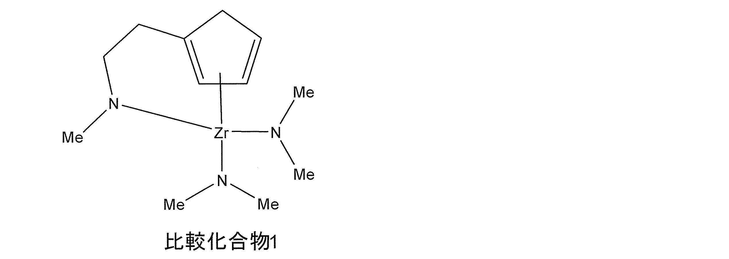
- Comparative Example 1 Production of Zirconium Oxide Thin Film by ALD Method Trial production of a zirconium oxide thin film on a silicon substrate was performed under the same conditions as in Example 1 except that the following comparative compound 1 was used as a raw material for chemical vapor deposition. .
- the film thickness measurement by the X-ray reflectivity method, the thin film structure and the thin film composition were confirmed by the X-ray diffraction method and the X-ray photoelectron spectroscopy.
- the thickness of the thin film in the portion where the groove was not formed was 3 to 4 nm, but the thin portion was formed with a non-uniform thickness in the groove portion (in the state where the thin film was not substantially formed at the bottom of the groove).
- the composition of the thin film was zirconium oxide (confirmed by the Zr3d and O1s peaks by XPS analysis), and the carbon content in the thin film was 8 atom%.
- the film thickness obtained per cycle was 0.02 to 0.04 nm.
- Comparative Example 2 Production of Zirconium Oxide Thin Film by ALD Method Trial production of a zirconium oxide thin film on a silicon substrate was performed under the same conditions as in Example 1 except that the following comparative compound 2 was used as a raw material for chemical vapor deposition. .
- the film thickness measurement by the X-ray reflectivity method, the thin film structure and the thin film composition were confirmed by the X-ray diffraction method and the X-ray photoelectron spectroscopy.
- the thickness of the thin film in the portion where the groove was not formed was 3 to 4 nm, but the thin portion was formed with a non-uniform thickness in the groove portion (in the state where the thin film was not substantially formed at the bottom of the groove).
- the composition of the thin film was zirconium oxide (confirmed by the Zr3d and O1s peaks by XPS analysis), and the carbon content in the thin film was 8 atom%.
- the film thickness obtained per cycle was 0.02 to 0.04 nm.
- Example 1 a high-quality zirconium oxide thin film could be obtained.
- Compound No. No. 34 has a high thermal stability, and it has been found that a high-quality thin film can be uniformly formed even in a groove portion having a high aspect ratio on the silicon substrate.
- Comparative Example 1 and Comparative Example 2 it is impossible to form a thin film with a uniform thickness in the groove portion having a high aspect ratio on the silicon substrate, and there are many carbon components remaining in the thin film. Thus, it was found that a high-quality zirconium oxide thin film could not be obtained.
- Example 2 Production of hafnium oxide thin film by ALD method A hafnium oxide thin film was produced on a silicon substrate having a groove having a diameter of 220 nm and a depth of 8600 nm by the ALD method under the following conditions using the ALD apparatus shown in FIG. About the obtained thin film, the film thickness measurement by X-ray reflectivity method, cross-sectional observation by FE-SEM, thin film structure and thin film composition were confirmed by X-ray diffraction method and X-ray photoelectron spectroscopy. The film thickness of the thin film in the portion where the groove was not formed was 3 to 6 nm, and the thin film was also formed in the groove portion with a uniform thickness.
- the composition of the thin film was hafnium oxide (confirmed by Hf4f and O1s peaks by XPS analysis), and the carbon content in the thin film was less than 0.1 atom% which is the lower limit of detection.
- the film thickness obtained per cycle was 0.02 to 0.04 nm.
- Example 3 Production of hafnium oxide thin film by ALD method A hafnium oxide thin film was produced on a silicon substrate under the same conditions as in Example 2 except that 66 was used as a raw material for chemical vapor deposition. About the obtained thin film, the film thickness measurement by X-ray reflectivity method, cross-sectional observation by FE-SEM, thin film structure and thin film composition were confirmed by X-ray diffraction method and X-ray photoelectron spectroscopy. The film thickness of the thin film in the portion where the groove was not formed was 3 to 6 nm, and the thin film was also formed in the groove portion with a uniform thickness.
- the composition of the thin film was hafnium oxide (confirmed by Hf4f and O1s peaks by XPS analysis), and the carbon content in the thin film was less than 0.1 atom% which is the lower limit of detection.
- the film thickness obtained per cycle was 0.02 to 0.04 nm.
Landscapes
- Chemical & Material Sciences (AREA)
- Organic Chemistry (AREA)
- General Chemical & Material Sciences (AREA)
- Chemical Kinetics & Catalysis (AREA)
- Engineering & Computer Science (AREA)
- Materials Engineering (AREA)
- Mechanical Engineering (AREA)
- Metallurgy (AREA)
- Inorganic Chemistry (AREA)
- Chemical Vapour Deposition (AREA)
- Formation Of Insulating Films (AREA)
Abstract
下記一般式(1)で表される化合物を含有してなる薄膜形成用原料。式中、R1は炭素原子数2~4の直鎖又は分岐状のアルキル基を表し、R2~R5は各々独立に炭素原子数1~4の直鎖又は分岐状のアルキル基を表し、Aは炭素原子数1~4のアルカンジイル基を表し、Mはチタン、ジルコニウム又はハフニウムを表す。ただし、Mがジルコニウムの場合は、Aは炭素原子数3又は4のアルカンジイル基である。Mがチタン及びハフニウムである場合、Aは炭素原子数2又は3のアルカンジイル基であることが好ましい。Mがジルコニウムである場合、Aは炭素原子数3のアルカンジイル基であることが好ましい。
Description
本発明は、特定の化合物を含有してなる薄膜形成用原料及び該薄膜形成用原料を用いた薄膜の製造方法に関する。
チタン、ジルコニウム又はハフニウムを含有する薄膜材料は、半導体、光電池、TFTなどの用途に応用されており、なかでも半導体材料用の高誘電材料として主に用いられている。
上記の薄膜の製造法としては、スパッタリング法、イオンプレーティング法、塗布熱分解法やゾルゲル法等のMOD法、化学気相成長法等が挙げられるが、組成制御性、段差被覆性に優れること、量産化に適すること、ハイブリッド集積が可能である等多くの長所を有しているので、ALD(Atomic Layer Deposition)法を含む化学気相成長(以下、単にCVDと記載することもある)法が最適な製造プロセスである。
化学気相成長法に用いられる金属供給源として、様々な原料が多数報告されている。
例えば、特許文献1には、CVD法やALD法に用いることができる材料として、特定のジルコニウム錯体を用いることが開示されている。また、特許文献2には、CVD法やALD法に用いることができる材料として、特定の金属錯体を用いることが開示されている。特許文献1及び特許文献2には、本発明の薄膜形成用原料について具体的な記載がない。
例えば、特許文献1には、CVD法やALD法に用いることができる材料として、特定のジルコニウム錯体を用いることが開示されている。また、特許文献2には、CVD法やALD法に用いることができる材料として、特定の金属錯体を用いることが開示されている。特許文献1及び特許文献2には、本発明の薄膜形成用原料について具体的な記載がない。
化学気相成長用原料等を気化させて基材表面に金属を含有する薄膜を形成する場合、高品質な薄膜を得るために高温下で成膜する必要があることから、熱安定性の高い薄膜形成用原料が求められている。また、アスペクト比が10~200程度の溝に均一に薄膜を形成することができる薄膜形成用原料が求められている。
本発明者等は、検討を重ねた結果、特定の化合物を含有する薄膜形成用原料が上記課題を解決し得ることを知見し、本発明に到達した。
本発明は、下記一般式(1)で表される化合物を含有してなる薄膜形成用原料を提供するものである。
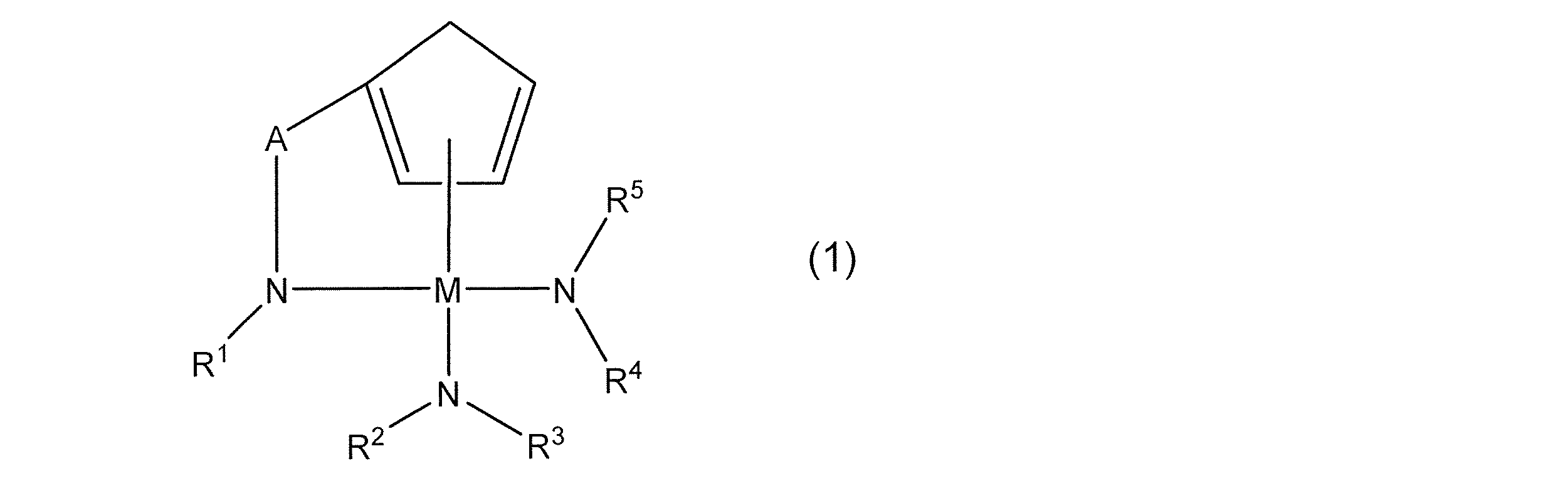
(式中、R1は炭素原子数2~4の直鎖又は分岐状のアルキル基を表し、R2~R5は各々独立に炭素原子数1~4の直鎖又は分岐状のアルキル基を表し、Aは炭素原子数1~4のアルカンジイル基を表し、Mはチタン、ジルコニウム又はハフニウムを表す。ただし、Mがジルコニウムの場合は、Aは炭素原子数3又は4のアルカンジイル基である。)
また、本発明は、上記薄膜形成用原料を気化させて得られる一般式(1)で表される化合物を含有する蒸気を、基体が設置された成膜チャンバー内に導入し、該化合物を分解及び/又は化学反応させて該基体の表面にチタン、ジルコニウム及びハフニウムから選ばれる少なくとも1種の原子を含有する薄膜を形成する薄膜の製造方法を提供するものである。
本発明によれば、熱安定性が高く、アスペクト比が10~200程度の溝に均一に高品質な薄膜を形成することができる薄膜形成用原料を得ることができる。本発明の薄膜形成用原料は、CVD法による金属薄膜形成用の原料として適している。本発明の薄膜形成用原料は、ALD法に適用可能であることから、上記効果を奏するALD法用薄膜形成用原料として特に適している。
本発明の薄膜形成用原料は、上記一般式(1)で表される化合物を含有するものであり、CVD法等の気化工程を有する薄膜製造方法のプレカーサとして好適なものであり、ALD法を用いて薄膜を形成することもできる。
上記一般式(1)において、R1は炭素原子数2~4の直鎖又は分岐状のアルキル基を表し、R2~R5は各々独立に炭素原子数1~4の直鎖又は分岐状のアルキル基を表し、Aは炭素原子数1~4のアルカンジイル基を表し、Mはチタン、ジルコニウム又はハフニウムを表す。ただし、Mがジルコニウムの場合は、Aは炭素原子数3又は4のアルカンジイル基である。
上記R1で表される炭素原子数2~4の直鎖又は分岐状のアルキル基としては、エチル、プロピル、イソプロピル、ブチル、イソブチル、第二ブチル、第三ブチル等が挙げられる。また、上記R2~R5で表される炭素原子数1~4の直鎖又は分岐状のアルキル基としては、メチル、エチル、プロピル、イソプロピル、ブチル、イソブチル、第二ブチル、第三ブチル等が挙げられる。
上記Aで表される炭素原子数1~4のアルカンジイル基としては、メチレン、エチレン、プロパン-1,3-ジイル、プロパン-1,2-ジイル、ブタン-1,4-ジイル、ブタン-1,3-ジイル等が挙げられる。上記Aで表される炭素原子数3又は4のアルカンジイル基としては、プロパン-1,3-ジイル、プロパン-1,2-ジイル、ブタン-1,4-ジイル、ブタン-1,3-ジイル等が挙げられる。
上記一般式(1)において、Mがチタン及びハフニウムである場合は、Aが炭素原子数2又は3のアルカンジイル基である場合は熱安定性が高く、ALD法を用いて成膜した場合に基体上のアスペクト比が高い溝の部分へ均一に薄膜を形成することができることから好ましく、なかでも、炭素原子数3のアルカンジイル基である場合は、ALD法を用いて成膜した場合に基体上のアスペクト比が高い溝の部分へ均一に薄膜を形成する効果が高いことから好ましい。Mがジルコニウムである場合は、Aが炭素原子数3のアルカンジイル基である場合は、ALD法を用いて成膜した場合に基体上のアスペクト比が高い溝の部分へ均一に薄膜を形成する効果が高いことから好ましい。上記一般式(1)において、R1がエチル、イソプロピル、第二ブチル及び第三ブチルのいずれかである場合は、ALD法を用いて成膜した場合に基体上のアスペクト比が高い溝の部分へ均一に薄膜を形成することができることから好ましい。R2~R5のうち1つ以上がメチル基である場合は蒸気圧が高いことから好ましい。なかでも、R2及びR4がメチルであり且つR3及びR5がエチルである場合は融点が低く、輸送性が良好なことから好ましい。気化工程を伴わないMOD法による薄膜の製造方法の場合は、R1~R5及びAは、使用される溶媒に対する溶解性、薄膜形成反応等によって適宜選択することができる。
一般式(1)で表される化合物の好ましい具体例としては、例えば、下記化学式No.1~No.88で表される化合物が挙げられる。なお、下記化学式No.1~No.88において「Me」はメチル基を表し、「Et」はエチル基を表し、「iPr」はイソプロピル基を表し、「sBu」は第二ブチル基を表し、「tBu」は第三ブチル基を表す。



本発明の薄膜形成用原料が含有する一般式(1)で表される化合物は、その製造方法により特に制限されることはなく、周知の反応を応用して製造される。例えば、Mがチタンの場合は、トルエン等の溶媒中でテトラキス(ジアルキルアミノ)チタンに、対応する構造のアルキルアミノアルキルシクロペンダジエン化合物を10~50℃の温度条件で反応させればよい。Mがジルコニウムの場合は、トルエン等の溶媒中でテトラキス(ジアルキルアミノ)ジルコニウムに、対応する構造のアルキルアミノアルキルシクロペンダジエン化合物を10~50℃の温度条件で反応させればよい。Mがハフニウムの場合は、トルエン等の溶媒中でテトラキス(ジアルキルアミノ)ハフニウムに、対応する構造のアルキルアミノアルキルシクロペンダジエン化合物を10~50℃の温度条件で反応させればよい。
本発明の薄膜形成用原料の形態は、該薄膜形成用原料が適用される製造プロセスによって異なる。例えば、チタン、ジルコニウム及びハフニウムからなる群から選ばれる金属のみを含む薄膜を製造する場合、本発明の薄膜形成用原料は、一般式(1)で表される化合物以外の金属化合物及び半金属化合物を非含有である。一方、チタン、ジルコニウム及びハフニウムからなる群から選ばれる金属とチタン、ジルコニウム及びハフニウムからなる群から選ばれる金属以外の金属及び/又は半金属とを含む薄膜を製造する場合、本発明の薄膜形成用原料は、チタン、ジルコニウム及びハフニウムからなる群から選ばれる金属以外の金属及び/又は半金属を含む化合物(以下、他のプレカーサともいう)を含有する。本発明の薄膜形成用原料は、後述するように、更に、有機溶剤及び/又は求核性試薬を含有してもよい。本発明の薄膜形成用原料は、上記説明のとおり、CVD法、ALD法に好適であるので、特に化学気相成長用原料(以下、CVD用原料ということもある)として有用である。
本発明の薄膜形成用原料が化学気相成長用原料である場合、その形態は使用されるCVD法の輸送供給方法等の手法により適宜選択されるものである。
上記の輸送供給方法としては、CVD用原料を該原料が貯蔵される容器(以下、単に原料容器と記載することもある)中で加熱及び/又は減圧することにより気化させて蒸気とし、必要に応じて用いられるアルゴン、窒素、ヘリウム等のキャリアガスと共に、該蒸気を基体が設置された成膜チャンバー内(以下、堆積反応部と記載することもある)へと導入する気体輸送法、CVD用原料を液体又は溶液の状態で気化室まで輸送し、気化室で加熱及び/又は減圧することにより気化させて蒸気とし、該蒸気を成膜チャンバー内へと導入する液体輸送法がある。気体輸送法の場合は、上記一般式(1)で表される化合物そのものをCVD用原料とすることができる。液体輸送法の場合は、上記一般式(1)で表される化合物そのもの又は該化合物を有機溶剤に溶かした溶液をCVD用原料とすることができる。これらのCVD用原料は更に他のプレカーサや求核性試薬等を含んでいてもよい。
また、多成分系のCVD法においては、CVD用原料を各成分独立で気化、供給する方法(以下、シングルソース法と記載することもある)と、多成分原料を予め所望の組成で混合した混合原料を気化、供給する方法(以下、カクテルソース法と記載することもある)がある。カクテルソース法の場合、本発明の薄膜形成用原料は、上記一般式(1)で表される化合物と他のプレカーサとの混合物若しくは該混合物を有機溶剤に溶かした混合溶液をCVD用原料とすることができる。この混合物や混合溶液は更に求核性試薬等を含んでいてもよい。
上記の有機溶剤としては、特に制限を受けることはなく周知一般の有機溶剤を用いることができる。該有機溶剤としては、例えば、酢酸エチル、酢酸ブチル、酢酸メトキシエチル等の酢酸エステル類;テトラヒドロフラン、テトラヒドロピラン、エチレングリコールジメチルエーテル、ジエチレングリコールジメチルエーテル、トリエチレングリコールジメチルエーテル、ジブチルエーテル、ジオキサン等のエーテル類;メチルブチルケトン、メチルイソブチルケトン、エチルブチルケトン、ジプロピルケトン、ジイソブチルケトン、メチルアミルケトン、シクロヘキサノン、メチルシクロヘキサノン等のケトン類;ヘキサン、シクロヘキサン、メチルシクロヘキサン、ジメチルシクロヘキサン、エチルシクロヘキサン、ヘプタン、オクタン、トルエン、キシレン等の炭化水素類;1-シアノプロパン、1-シアノブタン、1-シアノヘキサン、シアノシクロヘキサン、シアノベンゼン、1,3-ジシアノプロパン、1,4-ジシアノブタン、1,6-ジシアノヘキサン、1,4-ジシアノシクロヘキサン、1,4-ジシアノベンゼン等のシアノ基を有する炭化水素類;ピリジン、ルチジン等が挙げられる。これらの有機溶剤は、溶質の溶解性、使用温度と沸点、引火点の関係等に応じ、単独で用いてもよいし、又は二種類以上を混合して用いてもよい。これらの有機溶剤を使用する場合、プレカーサを有機溶剤に溶かした溶液であるCVD用原料中におけるプレカーサ全体の量が0.01~2.0モル/リットル、特に0.05~1.0モル/リットルとなるようにするのが好ましい。プレカーサ全体の量とは、本発明の薄膜形成用原料が、一般式(1)で表される化合物以外の金属化合物及び半金属化合物を非含有である場合、一般式(1)で表される化合物の量であり、本発明の薄膜形成用原料が、一般式(1)で表される化合物に加えて他の金属を含む化合物及び/又は半金属を含む化合物(他のプレカーサ)を含有する場合、一般式(1)で表される化合物及び他のプレカーサの合計量である。
また、多成分系のCVD法の場合において、本発明の薄膜形成用原料と共に用いられる他のプレカーサとしては、特に制限を受けず、CVD用原料に用いられている周知一般のプレカーサを用いることができる。
上記の他のプレカーサとしては、水素化物、水酸化物、ハロゲン化物、アジ化物、アルキル、アルケニル、シクロアルキル、アリール、アルキニル、アミノ、ジアルキルアミノアルキル、モノアルキルアミノ、ジアルキルアミノ、ジアミン、ジ(シリル-アルキル)アミノ、ジ(アルキル-シリル)アミノ、ジシリルアミノ、アルコキシ、アルコキシアルキル、ヒドラジド、ホスフィド、ニトリル、ジアルキルアミノアルコキシ、アルコキシアルキルジアルキルアミノ、シロキシ、ジケトナート、シクロペンタジエニル、シリル、ピラゾレート、グアニジネート、ホスホグアニジネート、アミジナート、ホスホアミジナート、ケトイミナート、ジケチミナート、カルボニル及びホスホアミジナートを配位子として有する化合物からなる群から選択される一種類又は二種類以上のケイ素や金属の化合物が挙げられる。
プレカーサの金属種としては、マグネシウム、カルシウム、ストロンチウム、バリウム、ラジウム、スカンジウム、イットリウム、バナジウム、ニオブ、タンタル、クロム、モリブデン、タングステン、マンガン、鉄、オスミウム、コバルト、ロジウム、イリジウム、ニッケル、パラジウム、白金、銅、銀、金、亜鉛、カドミウム、アルミニウム、ガリウム、インジウム、ゲルマニウム、スズ、鉛、アンチモン、ビスマス、ランタン、セリウム、プラセオジム、ネオジム、サマリウム、ユウロピウム、ガドリニウム、テルビウム、ジスプロシウム、ホルミウム、エルビウム、ツリウム、イッテルビウムが挙げられる。
上記の他のプレカーサは、当該技術分野において公知のものであり、その製造方法も公知である。製造方法の一例を挙げれば、例えば、有機配位子としてアルコール化合物を用いた場合には、先に述べた金属の無機塩又はその水和物と、該アルコール化合物のアルカリ金属アルコキシドとを反応させることによって、プレカーサを製造することができる。ここで、金属の無機塩又はその水和物としては、金属のハロゲン化物、硝酸塩等を挙げることができ、アルカリ金属アルコキシドとしては、ナトリウムアルコキシド、リチウムアルコキシド、カリウムアルコキシド等を挙げることができる。
上記の他のプレカーサは、シングルソース法の場合は、一般式(1)で表される化合物と、熱及び/又は酸化分解の挙動が類似している化合物が好ましく、カクテルソース法の場合は、熱及び/又は酸化分解の挙動が類似していることに加え、混合時に化学反応等による変質を起こさないものが好ましい。
上記の他のプレカーサとしては例えば、希土類元素を含むプレカーサを挙げることができる。希土類元素を含むプレカーサとしては、下記式(III-1)~(III~3)で表される化合物が挙げられる。

(式中、M2は、希土類原子を表し、Ra及びRbは各々独立に、ハロゲン原子で置換されてもよく、鎖中に酸素原子を含んでもよい炭素原子数1~20のアルキル基を表し、Rcは炭素原子数1~8のアルキル基を表し、Re及びRfは各々独立に、水素原子又は炭素原子数1~3のアルキル基を表し、Rg及びRjは各々独立に、炭素原子数1~4のアルキル基を表し、p’は0~3の整数を表し、r’は0~2の整数を表す。)
上記の希土類元素を含むプレカーサにおいて、M2で表される希土類原子としては、スカンジウム、イットリウム、ランタン、セリウム、プラセオジム、ネオジム、サマリウム、ユウロピウム、ガドリニウム、テルビウム、ジスプロシウム、ホルミウム、エルビウム、ツリウム、イッテルビウム、ルテチウム等が挙げられる。Ra及びRbで表される、ハロゲン原子で置換されてもよく、鎖中に酸素原子を含んでもよい炭素原子数1~20のアルキル基としては、メチル、エチル、プロピル、イソプロピル、ブチル、第二ブチル、第三ブチル、イソブチル、ペンチル、イソペンチル、ネオペンチル、第三ペンチル、ヘキシル、シクロヘキシル、1-メチルシクロヘキシル、ヘプチル、3-ヘプチル、イソヘプチル、第三ヘプチル、n-オクチル、イソオクチル、第三オクチル、2-エチルヘキシル、トリフルオロメチル、パーフルオロヘキシル、2-メトキシエチル、2-エトキシエチル、2-ブトキシエチル、2-(2-メトキシエトキシ)エチル、1-メトキシ-1,1-ジメチルメチル、2-メトキシ-1,1-ジメチルエチル、2-エトキシ-1,1-ジメチルエチル、2-イソプロポキシ-1,1-ジメチルエチル、2-ブトキシ-1,1-ジメチルエチル、2-(2-メトキシエトキシ)-1,1-ジメチルエチル等が挙げられる。また、Rcで表される炭素原子数1~8のアルキル基としては、メチル、エチル、プロピル、イソプロピル、ブチル、第二ブチル、第三ブチル、イソブチル、ペンチル、イソペンチル、ネオペンチル、第三ペンチル、ヘキシル、1-エチルペンチル、シクロヘキシル、1-メチルシクロヘキシル、ヘプチル、イソヘプチル、第三ヘプチル、n-オクチル、イソオクチル、第三オクチル、2-エチルヘキシル等が挙げられる。また、また、Re及びRfで表される炭素原子数1~3のアルキル基としては、メチル、エチル、プロピル、2-プロピル等が挙げられ、Rg及びRjで表される炭素原子数1~4のアルキル基としては、メチル、エチル、プロピル、イソプロピル、ブチル、第二ブチル、第三ブチル、イソブチル等が挙げられる。
また、本発明の薄膜形成用原料には、必要に応じて、上記一般式(1)で表される化合物及び他のプレカーサの安定性を付与するため、求核性試薬を含有してもよい。該求核性試薬としては、グライム、ジグライム、トリグライム、テトラグライム等のエチレングリコールエーテル類、18-クラウン-6、ジシクロヘキシル-18-クラウン-6、24-クラウン-8、ジシクロヘキシル-24-クラウン-8、ジベンゾ-24-クラウン-8等のクラウンエーテル類、エチレンジアミン、N,N’-テトラメチルエチレンジアミン、ジエチレントリアミン、トリエチレンテトラミン、テトラエチレンペンタミン、ペンタエチレンヘキサミン、1,1,4,7,7-ペンタメチルジエチレントリアミン、1,1,4,7,10,10-ヘキサメチルトリエチレンテトラミン、トリエトキシトリエチレンアミン等のポリアミン類、サイクラム、サイクレン等の環状ポリアミン類、ピリジン、ピロリジン、ピペリジン、モルホリン、N-メチルピロリジン、N-メチルピペリジン、N-メチルモルホリン、テトラヒドロフラン、テトラヒドロピラン、1,4-ジオキサン、オキサゾール、チアゾール、オキサチオラン等の複素環化合物類、アセト酢酸メチル、アセト酢酸エチル、アセト酢酸-2-メトキシエチル等のβ-ケトエステル類又はアセチルアセトン、2,4-ヘキサンジオン、2,4-ヘプタンジオン、3,5-ヘプタンジオン、ジピバロイルメタン等のβ-ジケトン類が挙げられる。これら求核性試薬の使用量は、プレカーサ全体の量1モルに対して0.1モル~10モルの範囲が好ましく、より好ましくは1~4モルである。
本発明の薄膜形成用原料には、これを構成する成分以外の不純物金属元素分、不純物塩素などの不純物ハロゲン分、及び不純物有機分が極力含まれないようにする。不純物金属元素分は、元素毎では100ppb以下が好ましく、10ppb以下がより好ましく、総量では、1ppm以下が好ましく、100ppb以下がより好ましい。特に、LSIのゲート絶縁膜、ゲート膜、バリア層として用いる場合は、得られる薄膜の電気的特性に影響のあるアルカリ金属元素及びアルカリ土類金属元素の含有量を少なくすることが必要である。不純物ハロゲン分は、100ppm以下が好ましく、10ppm以下がより好ましく、1ppm以下が最も好ましい。不純物有機分は、総量で500ppm以下が好ましく、50ppm以下がより好ましく、10ppm以下が最も好ましい。また、水分は、化学気相成長用原料中でのパーティクル発生や、薄膜形成中におけるパーティクル発生の原因となるので、金属化合物、有機溶剤及び求核性試薬については、それぞれの水分の低減のために、使用の際にあらかじめできる限り水分を取り除いた方がよい。金属化合物、有機溶剤及び求核性試薬それぞれの水分量は、10ppm以下が好ましく、1ppm以下がより好ましい。
また、本発明の薄膜形成用原料は、形成される薄膜のパーティクル汚染を低減又は防止するために、パーティクルが極力含まれないようにするのが好ましい。具体的には、液相での光散乱式液中粒子検出器によるパーティクル測定において、0.3μmより大きい粒子の数が液相1ml中に100個以下であることが好ましく、0.2μmより大きい粒子の数が液相1ml中に1000個以下であることがより好ましく、0.2μmより大きい粒子の数が液相1ml中に100個以下であることが最も好ましい。
本発明の薄膜形成用原料を用いて薄膜を製造する本発明の薄膜の製造方法としては、本発明の薄膜形成用原料を気化させた蒸気、及び必要に応じて用いられる反応性ガスを、基体が設置された成膜チャンバー内に導入し、次いで、プレカーサを基体上で分解及び/又は化学反応させて金属を含有する薄膜を基体表面に成長、堆積させるCVD法によるものである。原料の輸送供給方法、堆積方法、製造条件、製造装置等については、特に制限を受けるものではなく、周知一般の条件及び方法を用いることができる。
上記の必要に応じて用いられる反応性ガスとしては、例えば、酸化性のものとしては酸素、オゾン、二酸化窒素、一酸化窒素、水蒸気、過酸化水素、ギ酸、酢酸、無水酢酸等が挙げられ、還元性のものとしては水素が挙げられ、また、窒化物を製造するものとしては、モノアルキルアミン、ジアルキルアミン、トリアルキルアミン、アルキレンジアミン等の有機アミン化合物、ヒドラジン、アンモニア等が挙げられ、これらは1種類又は2種類以上使用することができる。
また、上記の輸送供給方法としては、前述した気体輸送法、液体輸送法、シングルソース法、カクテルソース法等が挙げられる。
また、上記の堆積方法としては、原料ガス又は原料ガスと反応性ガスを熱のみにより反応させ薄膜を堆積させる熱CVD、熱とプラズマを使用するプラズマCVD、熱と光を使用する光CVD、熱、光及びプラズマを使用する光プラズマCVD、CVDの堆積反応を素過程に分け、分子レベルで段階的に堆積を行うALDが挙げられる。
上記基体の材質としては、例えばシリコン;窒化ケイ素、窒化チタン、窒化タンタル、酸化チタン、窒化チタン、酸化ルテニウム、酸化ジルコニウム、酸化ハフニウム、酸化ランタン等のセラミックス;ガラス;金属ルテニウム等の金属が挙げられる。基体の形状としては、板状、球状、繊維状、鱗片状が挙げられ、基体表面は、平面であってもよく、アスペクト比が10~200程度のトレンチ(溝)を有するトレンチ構造等の三次元構造となっていてもよい。
また、上記の製造条件としては、反応温度(基体温度)、反応圧力、堆積速度等が挙げられる。反応温度については、一般式(1)で表される化合物が充分に反応する温度である100℃以上が好ましく、150℃~400℃がより好ましい。一般式(1)で表される化合物は300℃未満で熱分解させることができるので、150℃~250℃が特に好ましい。また、反応圧力は、熱CVD又は光CVDの場合、大気圧~10Paが好ましく、プラズマを使用する場合、2000Pa~10Paが好ましい。
また、堆積速度は、原料の供給条件(気化温度、気化圧力)、反応温度、反応圧力によりコントロールすることができる。堆積速度は、大きいと得られる薄膜の特性が悪化する場合があり、小さいと生産性に問題を生じる場合があるので、0.01~100nm/分が好ましく、1~50nm/分がより好ましい。また、ALD法の場合は、所望の膜厚が得られるようにサイクルの回数でコントロールされる。
また、堆積速度は、原料の供給条件(気化温度、気化圧力)、反応温度、反応圧力によりコントロールすることができる。堆積速度は、大きいと得られる薄膜の特性が悪化する場合があり、小さいと生産性に問題を生じる場合があるので、0.01~100nm/分が好ましく、1~50nm/分がより好ましい。また、ALD法の場合は、所望の膜厚が得られるようにサイクルの回数でコントロールされる。
上記の製造条件として更に、薄膜形成用原料を気化させて蒸気とする際の温度や圧力が挙げられる。薄膜形成用原料を気化させて蒸気とする工程は、原料容器内で行ってもよく、気化室内で行ってもよい。いずれの場合においても、本発明の薄膜形成用原料は0~150℃で蒸発させることが好ましい。また、原料容器内又は気化室内で薄膜形成用原料を気化させて蒸気とする場合に原料容器内の圧力及び気化室内の圧力はいずれも1~10000Paであることが好ましい。
本発明の薄膜の製造方法は、ALD法を採用して、上記の輸送供給方法により、薄膜形成用原料を気化させて蒸気とし、該蒸気を成膜チャンバー内へ導入する原料導入工程のほか、該蒸気中の上記一般式(1)で表される化合物により基体の表面に前駆体薄膜を形成する前駆体薄膜成膜工程、未反応の薄膜形成用原料ガスを排気する排気工程、及び、該前駆体薄膜を反応性ガスと化学反応させて、該基体の表面に金属を含有する薄膜を形成する金属含有薄膜形成工程を有していてもよい。
以下では、上記の各工程について、金属酸化物薄膜を形成する場合を例に詳しく説明する。金属酸化物薄膜をALD法により形成する場合は、まず、前記で説明した原料導入工程を行う。薄膜形成用原料を蒸気とする際の好ましい温度や圧力は上記で説明したものと同様である。次に、堆積反応部に導入した一般式(1)で表される化合物により、基体表面に前駆体薄膜を成膜させる(前駆体薄膜成膜工程)。このときに、基体を加熱するか、堆積反応部を加熱して、熱を加えてもよい。この工程で成膜される前駆体薄膜は、金属酸化物薄膜、又は、一般式(1)で表される化合物の一部が分解及び/又は反応して生成した薄膜であり、目的の金属酸化物薄膜とは異なる組成を有する。本工程が行われる際の基体温度は、室温~500℃が好ましく、150~350℃がより好ましい。本工程が行われる際の系(成膜チャンバー内)の圧力は1~10000Paが好ましく、10~1000Paがより好ましい。
次に、堆積反応部から、未反応の薄膜形成用原料ガスや副生したガスを排気する(排気工程)。未反応の薄膜形成用原料ガスや副生したガスは、堆積反応部から完全に排気されるのが理想的であるが、必ずしも完全に排気される必要はない。排気方法としては、窒素、ヘリウム、アルゴンなどの不活性ガスにより系内をパージする方法、系内を減圧することで排気する方法、これらを組み合わせた方法などが挙げられる。減圧する場合の減圧度は、0.01~300Paが好ましく、0.01~100Paがより好ましい。
次に、堆積反応部に酸化性ガスを導入し、該酸化性ガスの作用又は酸化性ガス及び熱の作用により、先の前駆体薄膜成膜工程で得た前駆体薄膜から金属酸化物薄膜を形成する(金属酸化物含有薄膜形成工程)。本工程において熱を作用させる場合の温度は、室温~500℃が好ましく、150~350℃がより好ましい。本工程が行われる際の系(成膜チャンバー内)の圧力は1~10000Paが好ましく、10~1000Paがより好ましい。本発明の薄膜形成用原料は、酸化性ガスとの反応性が良好であり、金属酸化物薄膜を得ることができる。
本発明の薄膜の製造方法において、上記のようにALD法を採用した場合、上記の原料導入工程、前駆体薄膜成膜工程、排気工程、及び、金属酸化物含有薄膜形成工程からなる一連の操作による薄膜堆積を1サイクルとし、このサイクルを必要な膜厚の薄膜が得られるまで複数回繰り返してもよい。この場合、1サイクル行った後、上記排気工程と同様にして、堆積反応部から未反応の薄膜形成用原料ガス及び反応性ガス(金属酸化物薄膜を形成する場合は酸化性ガス)、更に副生したガスを排気した後、次の1サイクルを行うことが好ましい。
また、金属酸化物薄膜のALD法による形成においては、プラズマ、光、電圧などのエネルギーを印加してもよく、触媒を用いてもよい。該エネルギーを印加する時期及び触媒を用いる時期は、特には限定されず、例えば、原料導入工程における本発明の薄膜形成用原料ガス導入時、前駆体薄膜成膜工程又は金属酸化物含有薄膜形成工程における加温時、排気工程における系内の排気時、金属酸化物含有薄膜形成工程における酸化性ガス導入時でもよく、上記の各工程の間でもよい。
また、本発明の薄膜の製造方法においては、薄膜堆積の後に、より良好な電気特性を得るために不活性雰囲気下、酸化性雰囲気下又は還元性雰囲気下でアニール処理を行ってもよく、段差埋め込みが必要な場合には、リフロー工程を設けてもよい。この場合の温度は、200~1000℃であり、250~500℃が好ましい。
本発明の薄膜形成用原料を用いて薄膜を製造する装置は、周知な化学気相成長法用装置を用いることができる。具体的な装置の例としては図1のようなプレカーサをバブリング供給で行うことのできる装置や、図2のように気化室を有する装置が挙げられる。また、図3及び図4のように反応性ガスに対してプラズマ処理を行うことのできる装置が挙げられる。図1~図4のような枚葉式装置に限らず、バッチ炉を用いた多数枚同時処理可能な装置を用いることもできる。
本発明の薄膜形成用原料を用いて製造される薄膜は、他のプレカーサ、反応性ガス及び製造条件を適宜選択することにより、メタル、酸化物セラミックス、窒化物セラミックス、ガラス等の所望の種類の薄膜とすることができる。該薄膜は種々の電気特性及び光学特性等を示すことが知られており、種々の用途に応用されている。例えば、半導体、光電池、TFTなどの用途に応用されており、なかでも半導体材料用の高誘電材料として主に用いられている。
以下、実施例及び評価例をもって本発明を更に詳細に説明する。しかしながら、本発明は以下の実施例等によって何ら制限を受けるものではない。
[実施例1]ALD法による酸化ジルコニウム薄膜の製造
化合物No.34を化学気相成長用原料とし、図1に示すALD装置を用いて以下の条件のALD法により、直径220nm、深さ8600nm(アスペクト比39.1)の溝を形成したシリコン基板上に酸化ジルコニウム薄膜を製造した。得られた薄膜について、X線反射率法による膜厚測定、FE-SEMによる断面観察、X線回折法及びX線光電子分光法による薄膜構造及び薄膜組成の確認を行った。溝が形成されていない部分における薄膜の膜厚は3~6nmであり、また、溝部分にも均一な厚みで薄膜が形成されていた。薄膜の組成は酸化ジルコニウム(XPS分析によるZr3d及びO1sのピークで確認)であり、また、薄膜中の炭素含有量は検出下限である0.1atom%よりも少なかった。1サイクル当たりに得られる膜厚は、0.02~0.04nmであった。
化合物No.34を化学気相成長用原料とし、図1に示すALD装置を用いて以下の条件のALD法により、直径220nm、深さ8600nm(アスペクト比39.1)の溝を形成したシリコン基板上に酸化ジルコニウム薄膜を製造した。得られた薄膜について、X線反射率法による膜厚測定、FE-SEMによる断面観察、X線回折法及びX線光電子分光法による薄膜構造及び薄膜組成の確認を行った。溝が形成されていない部分における薄膜の膜厚は3~6nmであり、また、溝部分にも均一な厚みで薄膜が形成されていた。薄膜の組成は酸化ジルコニウム(XPS分析によるZr3d及びO1sのピークで確認)であり、また、薄膜中の炭素含有量は検出下限である0.1atom%よりも少なかった。1サイクル当たりに得られる膜厚は、0.02~0.04nmであった。
(条件)
反応温度(基板温度):210℃、反応性ガス:オゾン
(工程)
下記(1)~(4)からなる一連の工程を1サイクルとして、150サイクル繰り返した。
(1)原料容器加熱温度140℃、原料容器内圧力10Paの条件で気化させた化学気相成長用原料の蒸気を導入し、系圧20Paで20秒間堆積させる。
(2)30秒間のアルゴンパージにより、未反応原料を除去する。
(3)反応性ガスを導入し、系圧力20Paで20秒間反応させる。
(4)30秒間のアルゴンパージにより、未反応原料を除去する。
反応温度(基板温度):210℃、反応性ガス:オゾン
(工程)
下記(1)~(4)からなる一連の工程を1サイクルとして、150サイクル繰り返した。
(1)原料容器加熱温度140℃、原料容器内圧力10Paの条件で気化させた化学気相成長用原料の蒸気を導入し、系圧20Paで20秒間堆積させる。
(2)30秒間のアルゴンパージにより、未反応原料を除去する。
(3)反応性ガスを導入し、系圧力20Paで20秒間反応させる。
(4)30秒間のアルゴンパージにより、未反応原料を除去する。
[比較例1]ALD法による酸化ジルコニウム薄膜の製造
下記の比較化合物1を化学気相成長法用原料とした以外は、実施例1と同じ条件でシリコン基板上に酸化ジルコニウム薄膜の製造を試みた。得られた薄膜について、X線反射率法による膜厚測定、X線回折法及びX線光電子分光法による薄膜構造及び薄膜組成の確認を行った。溝が形成されていない部分における薄膜の膜厚は3~4nmであったが、溝部分では不均一な厚みで薄膜が形成されていた(溝の底部には薄膜が略形成されていない状態であり、溝の底部以外には膜厚3~6nmの薄膜が形成されていた)。薄膜の組成は酸化ジルコニウム(XPS分析によるZr3d及びO1sのピークで確認)であり、また、薄膜中の炭素含有量は8atom%であった。1サイクル当たりに得られる膜厚は、0.02~0.04nmであった。
下記の比較化合物1を化学気相成長法用原料とした以外は、実施例1と同じ条件でシリコン基板上に酸化ジルコニウム薄膜の製造を試みた。得られた薄膜について、X線反射率法による膜厚測定、X線回折法及びX線光電子分光法による薄膜構造及び薄膜組成の確認を行った。溝が形成されていない部分における薄膜の膜厚は3~4nmであったが、溝部分では不均一な厚みで薄膜が形成されていた(溝の底部には薄膜が略形成されていない状態であり、溝の底部以外には膜厚3~6nmの薄膜が形成されていた)。薄膜の組成は酸化ジルコニウム(XPS分析によるZr3d及びO1sのピークで確認)であり、また、薄膜中の炭素含有量は8atom%であった。1サイクル当たりに得られる膜厚は、0.02~0.04nmであった。
[比較例2]ALD法による酸化ジルコニウム薄膜の製造
下記の比較化合物2を化学気相成長法用原料とした以外は、実施例1と同じ条件でシリコン基板上に酸化ジルコニウム薄膜の製造を試みた。得られた薄膜について、X線反射率法による膜厚測定、X線回折法及びX線光電子分光法による薄膜構造及び薄膜組成の確認を行った。溝が形成されていない部分における薄膜の膜厚は3~4nmであったが、溝部分では不均一な厚みで薄膜が形成されていた(溝の底部には薄膜が略形成されていない状態であり、溝の底部以外には膜厚3~6nmの薄膜が形成されていた)。薄膜の組成は酸化ジルコニウム(XPS分析によるZr3d及びO1sのピークで確認)であり、また、薄膜中の炭素含有量は8atom%であった。1サイクル当たりに得られる膜厚は、0.02~0.04nmであった。
下記の比較化合物2を化学気相成長法用原料とした以外は、実施例1と同じ条件でシリコン基板上に酸化ジルコニウム薄膜の製造を試みた。得られた薄膜について、X線反射率法による膜厚測定、X線回折法及びX線光電子分光法による薄膜構造及び薄膜組成の確認を行った。溝が形成されていない部分における薄膜の膜厚は3~4nmであったが、溝部分では不均一な厚みで薄膜が形成されていた(溝の底部には薄膜が略形成されていない状態であり、溝の底部以外には膜厚3~6nmの薄膜が形成されていた)。薄膜の組成は酸化ジルコニウム(XPS分析によるZr3d及びO1sのピークで確認)であり、また、薄膜中の炭素含有量は8atom%であった。1サイクル当たりに得られる膜厚は、0.02~0.04nmであった。

実施例1では、高品質な酸化ジルコニウム薄膜を得ることができた。また、化合物No.34は熱安定性が高いために、シリコン基板上のアスペクト比が高い溝の部分にも均一に高品質な薄膜を形成することができることがわかった。一方、比較例1及び比較例2では、シリコン基板上のアスペクト比が高い溝の部分に均一な厚みで薄膜を形成することができず、また、薄膜中に残留してしまう炭素成分が多いことから、高品質な酸化ジルコニウム薄膜を得ることができないということがわかった。
[実施例2]ALD法による酸化ハフニウム薄膜の製造
化合物No.58を化学気相成長用原料とし、図1に示すALD装置を用いて以下の条件のALD法により、直径220nm、深さ8600nmの溝を形成したシリコン基板上に酸化ハフニウム薄膜を製造した。得られた薄膜について、X線反射率法による膜厚測定、FE-SEMによる断面観察、X線回折法及びX線光電子分光法による薄膜構造及び薄膜組成の確認を行った。溝が形成されていない部分における薄膜の膜厚は3~6nmであり、また、溝部分にも均一な厚みで薄膜が形成されていた。薄膜の組成は酸化ハフニウム(XPS分析によるHf4f及びO1sピークで確認)であり、また、薄膜中の炭素含有量は検出下限である0.1atom%よりも少なかった。1サイクル当たりに得られる膜厚は、0.02~0.04nmであった。
化合物No.58を化学気相成長用原料とし、図1に示すALD装置を用いて以下の条件のALD法により、直径220nm、深さ8600nmの溝を形成したシリコン基板上に酸化ハフニウム薄膜を製造した。得られた薄膜について、X線反射率法による膜厚測定、FE-SEMによる断面観察、X線回折法及びX線光電子分光法による薄膜構造及び薄膜組成の確認を行った。溝が形成されていない部分における薄膜の膜厚は3~6nmであり、また、溝部分にも均一な厚みで薄膜が形成されていた。薄膜の組成は酸化ハフニウム(XPS分析によるHf4f及びO1sピークで確認)であり、また、薄膜中の炭素含有量は検出下限である0.1atom%よりも少なかった。1サイクル当たりに得られる膜厚は、0.02~0.04nmであった。
(条件)
反応温度(基板温度):280℃、反応性ガス:オゾン
(工程)
下記(1)~(4)からなる一連の工程を1サイクルとして、150サイクル繰り返した。
(1)原料容器加熱温度140℃、原料容器内圧力10Paの条件で気化させた化学気相成長用原料の蒸気を導入し、系圧20Paで20秒間堆積させる。
(2)30秒間のアルゴンパージにより、未反応原料を除去する。
(3)反応性ガスを導入し、系圧力20Paで20秒間反応させる。
(4)30秒間のアルゴンパージにより、未反応原料を除去する。
反応温度(基板温度):280℃、反応性ガス:オゾン
(工程)
下記(1)~(4)からなる一連の工程を1サイクルとして、150サイクル繰り返した。
(1)原料容器加熱温度140℃、原料容器内圧力10Paの条件で気化させた化学気相成長用原料の蒸気を導入し、系圧20Paで20秒間堆積させる。
(2)30秒間のアルゴンパージにより、未反応原料を除去する。
(3)反応性ガスを導入し、系圧力20Paで20秒間反応させる。
(4)30秒間のアルゴンパージにより、未反応原料を除去する。
[実施例3]ALD法による酸化ハフニウム薄膜の製造
化合物No.66を化学気相成長法用原料とした以外は、実施例2と同じ条件でシリコン基板上に酸化ハフニウム薄膜を製造した。得られた薄膜について、X線反射率法による膜厚測定、FE-SEMによる断面観察、X線回折法及びX線光電子分光法による薄膜構造及び薄膜組成の確認を行った。溝が形成されていない部分における薄膜の膜厚は3~6nmであり、また、溝部分にも均一な厚みで薄膜が形成されていた。薄膜の組成は酸化ハフニウム(XPS分析によるHf4f及びO1sピークで確認)であり、また、薄膜中の炭素含有量は検出下限である0.1atom%よりも少なかった。1サイクル当たりに得られる膜厚は、0.02~0.04nmであった。
化合物No.66を化学気相成長法用原料とした以外は、実施例2と同じ条件でシリコン基板上に酸化ハフニウム薄膜を製造した。得られた薄膜について、X線反射率法による膜厚測定、FE-SEMによる断面観察、X線回折法及びX線光電子分光法による薄膜構造及び薄膜組成の確認を行った。溝が形成されていない部分における薄膜の膜厚は3~6nmであり、また、溝部分にも均一な厚みで薄膜が形成されていた。薄膜の組成は酸化ハフニウム(XPS分析によるHf4f及びO1sピークで確認)であり、また、薄膜中の炭素含有量は検出下限である0.1atom%よりも少なかった。1サイクル当たりに得られる膜厚は、0.02~0.04nmであった。
実施例2及び3では、いずれも高品質な酸化ハフニウム薄膜を得ることができた。また、化合物No.58及び66は熱安定性が高いために、シリコン基板上のアスペクト比が高い溝の部分にも均一に高品質な薄膜を形成することができることがわかった。
なお、本国際出願は、2016年5月23日に出願した日本国特許出願第2016-102628号に基づく優先権を主張するものであり、この日本国特許出願の全内容を本国際出願に援用する。
Claims (3)
- 下記一般式(1)で表される化合物を含有してなる薄膜形成用原料。

- ALD法用薄膜形成用原料である請求項1に記載の薄膜形成用原料。
- 請求項1又は2に記載の薄膜形成用原料を気化させて得られる一般式(1)で表される化合物を含有する蒸気を、基体が設置された成膜チャンバー内に導入し、該化合物を分解及び/又は化学反応させて該基体の表面にチタン、ジルコニウム及びハフニウムから選ばれる少なくとも1種の原子を含有する薄膜を形成する薄膜の製造方法。
Priority Applications (3)
| Application Number | Priority Date | Filing Date | Title |
|---|---|---|---|
| CN201780031611.4A CN109154080B (zh) | 2016-05-23 | 2017-02-27 | 薄膜形成用原料及薄膜的制造方法 |
| KR1020187036266A KR102724144B1 (ko) | 2016-05-23 | 2017-02-27 | 박막 형성용 원료 및 박막의 제조 방법 |
| US16/302,895 US10927460B2 (en) | 2016-05-23 | 2017-02-27 | Raw material for forming thin film, and method for manufacturing thin film |
Applications Claiming Priority (2)
| Application Number | Priority Date | Filing Date | Title |
|---|---|---|---|
| JP2016102628A JP6796950B2 (ja) | 2016-05-23 | 2016-05-23 | 薄膜形成用原料及び薄膜の製造方法 |
| JP2016-102628 | 2016-05-23 |
Publications (1)
| Publication Number | Publication Date |
|---|---|
| WO2017203775A1 true WO2017203775A1 (ja) | 2017-11-30 |
Family
ID=60412261
Family Applications (1)
| Application Number | Title | Priority Date | Filing Date |
|---|---|---|---|
| PCT/JP2017/007483 Ceased WO2017203775A1 (ja) | 2016-05-23 | 2017-02-27 | 薄膜形成用原料及び薄膜の製造方法 |
Country Status (6)
| Country | Link |
|---|---|
| US (1) | US10927460B2 (ja) |
| JP (1) | JP6796950B2 (ja) |
| KR (1) | KR102724144B1 (ja) |
| CN (1) | CN109154080B (ja) |
| TW (1) | TWI761333B (ja) |
| WO (1) | WO2017203775A1 (ja) |
Families Citing this family (5)
| Publication number | Priority date | Publication date | Assignee | Title |
|---|---|---|---|---|
| US10465289B2 (en) * | 2016-12-30 | 2019-11-05 | L'Air Liquide, Société Anonyme pour l'Etude at l'Exploitation des Procédés Georges Claude | Zirconium, hafnium, titanium precursors and deposition of group 4 containing films using the same |
| JP7240903B2 (ja) * | 2019-03-05 | 2023-03-16 | レール・リキード-ソシエテ・アノニム・プール・レテュード・エ・レクスプロワタシオン・デ・プロセデ・ジョルジュ・クロード | インジウム化合物および該インジウム化合物を用いたインジウム含有膜の成膜方法 |
| KR102627457B1 (ko) * | 2019-08-06 | 2024-01-19 | 삼성전자주식회사 | 나이오븀 화합물과 이를 이용하는 박막 형성 방법 |
| JP7246284B2 (ja) * | 2019-08-15 | 2023-03-27 | 東京エレクトロン株式会社 | 成膜方法 |
| KR102815650B1 (ko) * | 2023-06-30 | 2025-05-30 | 에스케이트리켐 주식회사 | 4족 전이금속 함유 박막 형성용 전구체 및 이를 이용한 4족 전이금속 함유 박막 형성 방법. |
Citations (2)
| Publication number | Priority date | Publication date | Assignee | Title |
|---|---|---|---|---|
| JP2014510733A (ja) * | 2011-03-15 | 2014-05-01 | メカロニックス シーオー. エルティディ. | 新規な4b族有機金属化合物及びその製造方法 |
| KR20140078534A (ko) * | 2012-12-17 | 2014-06-25 | 솔브레인씨그마알드리치 유한회사 | 금속 전구체 및 이를 이용하여 제조된 금속 함유 박막 |
Family Cites Families (3)
| Publication number | Priority date | Publication date | Assignee | Title |
|---|---|---|---|---|
| KR101395644B1 (ko) * | 2012-02-08 | 2014-05-16 | 주식회사 메카로닉스 | 신규한 4-비이 족 금속 유기화합물 및 그 제조방법 |
| KR101263454B1 (ko) | 2011-03-15 | 2013-11-27 | 주식회사 메카로닉스 | 지르코늄 금속을 함유하는 신규한 유기금속화합물 및 그 제조방법 |
| KR102147190B1 (ko) * | 2015-03-20 | 2020-08-25 | 에스케이하이닉스 주식회사 | 막형성조성물 및 그를 이용한 박막 제조 방법 |
-
2016
- 2016-05-23 JP JP2016102628A patent/JP6796950B2/ja active Active
-
2017
- 2017-02-27 CN CN201780031611.4A patent/CN109154080B/zh active Active
- 2017-02-27 KR KR1020187036266A patent/KR102724144B1/ko active Active
- 2017-02-27 US US16/302,895 patent/US10927460B2/en active Active
- 2017-02-27 WO PCT/JP2017/007483 patent/WO2017203775A1/ja not_active Ceased
- 2017-03-06 TW TW106107233A patent/TWI761333B/zh active
Patent Citations (2)
| Publication number | Priority date | Publication date | Assignee | Title |
|---|---|---|---|---|
| JP2014510733A (ja) * | 2011-03-15 | 2014-05-01 | メカロニックス シーオー. エルティディ. | 新規な4b族有機金属化合物及びその製造方法 |
| KR20140078534A (ko) * | 2012-12-17 | 2014-06-25 | 솔브레인씨그마알드리치 유한회사 | 금속 전구체 및 이를 이용하여 제조된 금속 함유 박막 |
Non-Patent Citations (1)
| Title |
|---|
| CHIRINOS,J. ET AL.: "Ethene homo- and ethene/propene copolymerization using a MAO activated cyclopentadienyl-amido half-sandwich complex", MACROMOLECULAR CHEMISTRY AND PHYSICS, vol. 201, no. 7, November 2000 (2000-11-01), pages 2581 - 2585, XP055509605 * |
Also Published As
| Publication number | Publication date |
|---|---|
| US10927460B2 (en) | 2021-02-23 |
| JP2017210632A (ja) | 2017-11-30 |
| KR20190009328A (ko) | 2019-01-28 |
| US20190292663A1 (en) | 2019-09-26 |
| KR102724144B1 (ko) | 2024-10-30 |
| JP6796950B2 (ja) | 2020-12-09 |
| TWI761333B (zh) | 2022-04-21 |
| TW201808970A (zh) | 2018-03-16 |
| CN109154080A (zh) | 2019-01-04 |
| CN109154080B (zh) | 2021-05-11 |
Similar Documents
| Publication | Publication Date | Title |
|---|---|---|
| KR102441169B1 (ko) | 디아자디에닐 화합물, 박막 형성용 원료, 박막의 제조 방법 및 디아자디엔 화합물 | |
| KR102280110B1 (ko) | 바나듐 화합물, 박막 형성용 원료 및 박막의 제조 방법 | |
| WO2019203035A1 (ja) | 原子層堆積法用薄膜形成用原料及び薄膜の製造方法 | |
| KR102724144B1 (ko) | 박막 형성용 원료 및 박막의 제조 방법 | |
| WO2014103588A1 (ja) | アルミニウム化合物、薄膜形成用原料及び薄膜の製造方法 | |
| JP7717051B2 (ja) | 原子層堆積法用薄膜形成用原料及び薄膜の製造方法 | |
| CN110831950B (zh) | 钨化合物、薄膜形成用原料和薄膜的制造方法 | |
| JPWO2018235530A1 (ja) | 金属アルコキシド化合物、薄膜形成用原料及び薄膜の製造方法 | |
| JP5912911B2 (ja) | アルミニウム化合物を用いたald法による薄膜の製造方法 | |
| JP6760822B2 (ja) | 化合物、薄膜形成用原料、原子層堆積法用の薄膜形成用原料及び薄膜の製造方法 | |
| JP6272033B2 (ja) | 原子層堆積法による酸化ケイ素又は酸窒化ケイ素薄膜の製造方法 | |
| JP6116007B2 (ja) | 薄膜形成用原料及び薄膜の製造方法 | |
| KR102875898B1 (ko) | 아연 화합물, 박막 형성용 원료, 박막 및 그 제조 방법 | |
| JP4107923B2 (ja) | イットリウム含有複合酸化物薄膜の製造方法 | |
| JP2018203641A (ja) | 新規な化合物、薄膜形成用原料及び薄膜の製造方法 | |
| WO2018008351A1 (ja) | 金属炭化物含有薄膜形成用原料及び金属炭化物含有薄膜の製造方法 | |
| JP6704808B2 (ja) | 薄膜形成用原料及び薄膜の製造方法 | |
| JP7516092B2 (ja) | 薄膜形成原料、薄膜及びその製造方法 | |
| JP2018083771A (ja) | 化合物、薄膜形成用原料及び薄膜の製造方法 |
Legal Events
| Date | Code | Title | Description |
|---|---|---|---|
| NENP | Non-entry into the national phase |
Ref country code: DE |
|
| 121 | Ep: the epo has been informed by wipo that ep was designated in this application |
Ref document number: 17802377 Country of ref document: EP Kind code of ref document: A1 |
|
| ENP | Entry into the national phase |
Ref document number: 20187036266 Country of ref document: KR Kind code of ref document: A |
|
| 122 | Ep: pct application non-entry in european phase |
Ref document number: 17802377 Country of ref document: EP Kind code of ref document: A1 |