WO2017199768A1 - レジスト下層膜形成組成物 - Google Patents
レジスト下層膜形成組成物 Download PDFInfo
- Publication number
- WO2017199768A1 WO2017199768A1 PCT/JP2017/017272 JP2017017272W WO2017199768A1 WO 2017199768 A1 WO2017199768 A1 WO 2017199768A1 JP 2017017272 W JP2017017272 W JP 2017017272W WO 2017199768 A1 WO2017199768 A1 WO 2017199768A1
- Authority
- WO
- WIPO (PCT)
- Prior art keywords
- group
- resist underlayer
- underlayer film
- forming composition
- film forming
- Prior art date
- Legal status (The legal status is an assumption and is not a legal conclusion. Google has not performed a legal analysis and makes no representation as to the accuracy of the status listed.)
- Ceased
Links
Images


Classifications
-
- C—CHEMISTRY; METALLURGY
- C08—ORGANIC MACROMOLECULAR COMPOUNDS; THEIR PREPARATION OR CHEMICAL WORKING-UP; COMPOSITIONS BASED THEREON
- C08G—MACROMOLECULAR COMPOUNDS OBTAINED OTHERWISE THAN BY REACTIONS ONLY INVOLVING UNSATURATED CARBON-TO-CARBON BONDS
- C08G8/00—Condensation polymers of aldehydes or ketones with phenols only
- C08G8/04—Condensation polymers of aldehydes or ketones with phenols only of aldehydes
-
- G—PHYSICS
- G03—PHOTOGRAPHY; CINEMATOGRAPHY; ANALOGOUS TECHNIQUES USING WAVES OTHER THAN OPTICAL WAVES; ELECTROGRAPHY; HOLOGRAPHY
- G03F—PHOTOMECHANICAL PRODUCTION OF TEXTURED OR PATTERNED SURFACES, e.g. FOR PRINTING, FOR PROCESSING OF SEMICONDUCTOR DEVICES; MATERIALS THEREFOR; ORIGINALS THEREFOR; APPARATUS SPECIALLY ADAPTED THEREFOR
- G03F7/00—Photomechanical, e.g. photolithographic, production of textured or patterned surfaces, e.g. printing surfaces; Materials therefor, e.g. comprising photoresists; Apparatus specially adapted therefor
- G03F7/004—Photosensitive materials
- G03F7/09—Photosensitive materials characterised by structural details, e.g. supports, auxiliary layers
- G03F7/11—Photosensitive materials characterised by structural details, e.g. supports, auxiliary layers having cover layers or intermediate layers, e.g. subbing layers
-
- C—CHEMISTRY; METALLURGY
- C08—ORGANIC MACROMOLECULAR COMPOUNDS; THEIR PREPARATION OR CHEMICAL WORKING-UP; COMPOSITIONS BASED THEREON
- C08G—MACROMOLECULAR COMPOUNDS OBTAINED OTHERWISE THAN BY REACTIONS ONLY INVOLVING UNSATURATED CARBON-TO-CARBON BONDS
- C08G8/00—Condensation polymers of aldehydes or ketones with phenols only
-
- C—CHEMISTRY; METALLURGY
- C08—ORGANIC MACROMOLECULAR COMPOUNDS; THEIR PREPARATION OR CHEMICAL WORKING-UP; COMPOSITIONS BASED THEREON
- C08G—MACROMOLECULAR COMPOUNDS OBTAINED OTHERWISE THAN BY REACTIONS ONLY INVOLVING UNSATURATED CARBON-TO-CARBON BONDS
- C08G8/00—Condensation polymers of aldehydes or ketones with phenols only
- C08G8/04—Condensation polymers of aldehydes or ketones with phenols only of aldehydes
- C08G8/08—Condensation polymers of aldehydes or ketones with phenols only of aldehydes of formaldehyde, e.g. of formaldehyde formed in situ
- C08G8/10—Condensation polymers of aldehydes or ketones with phenols only of aldehydes of formaldehyde, e.g. of formaldehyde formed in situ with phenol
-
- C—CHEMISTRY; METALLURGY
- C09—DYES; PAINTS; POLISHES; NATURAL RESINS; ADHESIVES; COMPOSITIONS NOT OTHERWISE PROVIDED FOR; APPLICATIONS OF MATERIALS NOT OTHERWISE PROVIDED FOR
- C09D—COATING COMPOSITIONS, e.g. PAINTS, VARNISHES OR LACQUERS; FILLING PASTES; CHEMICAL PAINT OR INK REMOVERS; INKS; CORRECTING FLUIDS; WOODSTAINS; PASTES OR SOLIDS FOR COLOURING OR PRINTING; USE OF MATERIALS THEREFOR
- C09D161/00—Coating compositions based on condensation polymers of aldehydes or ketones; Coating compositions based on derivatives of such polymers
- C09D161/04—Condensation polymers of aldehydes or ketones with phenols only
-
- C—CHEMISTRY; METALLURGY
- C09—DYES; PAINTS; POLISHES; NATURAL RESINS; ADHESIVES; COMPOSITIONS NOT OTHERWISE PROVIDED FOR; APPLICATIONS OF MATERIALS NOT OTHERWISE PROVIDED FOR
- C09D—COATING COMPOSITIONS, e.g. PAINTS, VARNISHES OR LACQUERS; FILLING PASTES; CHEMICAL PAINT OR INK REMOVERS; INKS; CORRECTING FLUIDS; WOODSTAINS; PASTES OR SOLIDS FOR COLOURING OR PRINTING; USE OF MATERIALS THEREFOR
- C09D161/00—Coating compositions based on condensation polymers of aldehydes or ketones; Coating compositions based on derivatives of such polymers
- C09D161/04—Condensation polymers of aldehydes or ketones with phenols only
- C09D161/06—Condensation polymers of aldehydes or ketones with phenols only of aldehydes with phenols
-
- G—PHYSICS
- G03—PHOTOGRAPHY; CINEMATOGRAPHY; ANALOGOUS TECHNIQUES USING WAVES OTHER THAN OPTICAL WAVES; ELECTROGRAPHY; HOLOGRAPHY
- G03F—PHOTOMECHANICAL PRODUCTION OF TEXTURED OR PATTERNED SURFACES, e.g. FOR PRINTING, FOR PROCESSING OF SEMICONDUCTOR DEVICES; MATERIALS THEREFOR; ORIGINALS THEREFOR; APPARATUS SPECIALLY ADAPTED THEREFOR
- G03F7/00—Photomechanical, e.g. photolithographic, production of textured or patterned surfaces, e.g. printing surfaces; Materials therefor, e.g. comprising photoresists; Apparatus specially adapted therefor
- G03F7/004—Photosensitive materials
- G03F7/09—Photosensitive materials characterised by structural details, e.g. supports, auxiliary layers
- G03F7/094—Multilayer resist systems, e.g. planarising layers
-
- G—PHYSICS
- G03—PHOTOGRAPHY; CINEMATOGRAPHY; ANALOGOUS TECHNIQUES USING WAVES OTHER THAN OPTICAL WAVES; ELECTROGRAPHY; HOLOGRAPHY
- G03F—PHOTOMECHANICAL PRODUCTION OF TEXTURED OR PATTERNED SURFACES, e.g. FOR PRINTING, FOR PROCESSING OF SEMICONDUCTOR DEVICES; MATERIALS THEREFOR; ORIGINALS THEREFOR; APPARATUS SPECIALLY ADAPTED THEREFOR
- G03F7/00—Photomechanical, e.g. photolithographic, production of textured or patterned surfaces, e.g. printing surfaces; Materials therefor, e.g. comprising photoresists; Apparatus specially adapted therefor
- G03F7/16—Coating processes; Apparatus therefor
-
- H—ELECTRICITY
- H10—SEMICONDUCTOR DEVICES; ELECTRIC SOLID-STATE DEVICES NOT OTHERWISE PROVIDED FOR
- H10P—GENERIC PROCESSES OR APPARATUS FOR THE MANUFACTURE OR TREATMENT OF DEVICES COVERED BY CLASS H10
- H10P14/00—Formation of materials, e.g. in the shape of layers or pillars
- H10P14/60—Formation of materials, e.g. in the shape of layers or pillars of insulating materials
- H10P14/63—Formation of materials, e.g. in the shape of layers or pillars of insulating materials characterised by the formation processes
- H10P14/6326—Deposition processes
- H10P14/6342—Liquid deposition, e.g. spin-coating, sol-gel techniques or spray coating
-
- H—ELECTRICITY
- H10—SEMICONDUCTOR DEVICES; ELECTRIC SOLID-STATE DEVICES NOT OTHERWISE PROVIDED FOR
- H10P—GENERIC PROCESSES OR APPARATUS FOR THE MANUFACTURE OR TREATMENT OF DEVICES COVERED BY CLASS H10
- H10P14/00—Formation of materials, e.g. in the shape of layers or pillars
- H10P14/60—Formation of materials, e.g. in the shape of layers or pillars of insulating materials
- H10P14/68—Organic materials, e.g. photoresists
- H10P14/683—Organic materials, e.g. photoresists carbon-based polymeric organic materials, e.g. polyimides, poly cyclobutene or PVC
-
- H—ELECTRICITY
- H10—SEMICONDUCTOR DEVICES; ELECTRIC SOLID-STATE DEVICES NOT OTHERWISE PROVIDED FOR
- H10P—GENERIC PROCESSES OR APPARATUS FOR THE MANUFACTURE OR TREATMENT OF DEVICES COVERED BY CLASS H10
- H10P50/00—Etching of wafers, substrates or parts of devices
- H10P50/20—Dry etching; Plasma etching; Reactive-ion etching
- H10P50/28—Dry etching; Plasma etching; Reactive-ion etching of insulating materials
- H10P50/286—Dry etching; Plasma etching; Reactive-ion etching of insulating materials of organic materials
- H10P50/287—Dry etching; Plasma etching; Reactive-ion etching of insulating materials of organic materials by chemical means
-
- H—ELECTRICITY
- H10—SEMICONDUCTOR DEVICES; ELECTRIC SOLID-STATE DEVICES NOT OTHERWISE PROVIDED FOR
- H10P—GENERIC PROCESSES OR APPARATUS FOR THE MANUFACTURE OR TREATMENT OF DEVICES COVERED BY CLASS H10
- H10P50/00—Etching of wafers, substrates or parts of devices
- H10P50/73—Etching of wafers, substrates or parts of devices using masks for insulating materials
-
- H—ELECTRICITY
- H10—SEMICONDUCTOR DEVICES; ELECTRIC SOLID-STATE DEVICES NOT OTHERWISE PROVIDED FOR
- H10P—GENERIC PROCESSES OR APPARATUS FOR THE MANUFACTURE OR TREATMENT OF DEVICES COVERED BY CLASS H10
- H10P76/00—Manufacture or treatment of masks on semiconductor bodies, e.g. by lithography or photolithography
-
- H—ELECTRICITY
- H10—SEMICONDUCTOR DEVICES; ELECTRIC SOLID-STATE DEVICES NOT OTHERWISE PROVIDED FOR
- H10P—GENERIC PROCESSES OR APPARATUS FOR THE MANUFACTURE OR TREATMENT OF DEVICES COVERED BY CLASS H10
- H10P76/00—Manufacture or treatment of masks on semiconductor bodies, e.g. by lithography or photolithography
- H10P76/20—Manufacture or treatment of masks on semiconductor bodies, e.g. by lithography or photolithography of masks comprising organic materials
- H10P76/204—Manufacture or treatment of masks on semiconductor bodies, e.g. by lithography or photolithography of masks comprising organic materials of organic photoresist masks
- H10P76/2041—Photolithographic processes
- H10P76/2043—Photolithographic processes using an anti-reflective coating
-
- G—PHYSICS
- G03—PHOTOGRAPHY; CINEMATOGRAPHY; ANALOGOUS TECHNIQUES USING WAVES OTHER THAN OPTICAL WAVES; ELECTROGRAPHY; HOLOGRAPHY
- G03F—PHOTOMECHANICAL PRODUCTION OF TEXTURED OR PATTERNED SURFACES, e.g. FOR PRINTING, FOR PROCESSING OF SEMICONDUCTOR DEVICES; MATERIALS THEREFOR; ORIGINALS THEREFOR; APPARATUS SPECIALLY ADAPTED THEREFOR
- G03F7/00—Photomechanical, e.g. photolithographic, production of textured or patterned surfaces, e.g. printing surfaces; Materials therefor, e.g. comprising photoresists; Apparatus specially adapted therefor
- G03F7/16—Coating processes; Apparatus therefor
- G03F7/162—Coating on a rotating support, e.g. using a whirler or a spinner
Definitions
- the present invention relates to a resist underlayer film forming composition for a lithography process.
- the present invention relates to a composition for forming a resist underlayer film having etching resistance when used as a mask material and having a surface embedding property with a step, a concave portion and / or a convex portion.
- fine processing is performed by a lithography process.
- lithography process when the resist layer on the substrate is exposed with an ultraviolet laser such as a KrF excimer laser or an ArF excimer laser, it is desired to be affected by the standing wave generated by the reflection of the ultraviolet laser on the substrate surface.
- an ultraviolet laser such as a KrF excimer laser or an ArF excimer laser
- a resist pattern having the following shape is not formed.
- it is adopted to provide a resist underlayer film (antireflection film) between the substrate and the resist layer.
- a novolak resin as a composition for forming a resist underlayer film (patent document 1, patent document 2, patent document 3, and patent document 4).
- a lithography process is also known in which at least two resist underlayer films are formed and the resist underlayer films are used as a mask material in order to reduce the thickness of the resist layer required in accordance with the miniaturization of the resist pattern.
- the material forming the at least two layers include organic resins (for example, acrylic resin, novolac resin), silicon resins (for example, organopolysiloxane), and inorganic silicon compounds (for example, SiON, SiO 2 ).
- organic resins for example, acrylic resin, novolac resin
- silicon resins for example, organopolysiloxane
- inorganic silicon compounds for example, SiON, SiO 2
- Patent Document 1 Patent Document 2, and Patent Document 3 disclose organic resins that can form such patterns and have embedding properties.
- JP 2014-24831 A International Publication No. 2014/024836 International Publication No. 2013/146670 International Publication No. 2010/147155
- methyl 2-hydroxyisobutyrate may be used as a solvent.
- the coater used to apply the resist underlayer film forming composition onto the substrate is continued with 2-hydroxyisobutyric acid.
- the drain pipe connected to the coater is clogged and the waste liquid cannot be discharged. This problem is caused by deposits of the resist underlayer film forming composition formed by mixing the resist underlayer film forming composition and methyl 2-hydroxyisobutyrate in the pipe.
- the first aspect of the present invention is the following formula (1a) and / or formula (1b): [In the formulas (1a) and (1b), two R 1 s are each independently an alkyl group having 1 to 10 carbon atoms, an alkenyl group having 2 to 6 carbon atoms, an aromatic hydrocarbon group, a halogen atom, or a nitro group.
- R 2 each independently represent a hydrogen atom or an alkyl group having 1 to 10 carbon atoms, an alkenyl group, an acetal group of 2 to 6 carbon atoms, an acyl group or a glycidyl group
- R 3 Represents an optionally substituted aromatic hydrocarbon group or heterocyclic group
- R 4 represents a hydrogen atom, a phenyl group or a naphthyl group
- R 3 and R 4 bonded to the same carbon atom are each phenyl.
- the polymer necessarily has a repeating structural unit represented by the formula (1a), and may optionally have a repeating structural unit represented by the formula (1b).
- R 1 represents a halogen atom
- examples of the halogen atom include a chlorine atom and a bromine atom.
- the aromatic ring of the aromatic hydrocarbon group may be monocyclic, polycyclic (including bicyclic), or heterocyclic, such as phenyl, biphenyl, naphthyl, anthryl, pyrenyl, thienyl, pyridyl. Groups.
- the aromatic hydrocarbon group which may have a substituent represented by R 3 a phenyl group, a naphthyl group, an anthryl group and a pyrenyl group are preferable from the viewpoint of etching resistance and embedding property.
- a substituent of an aromatic hydrocarbon group a methoxy group and an aldehyde group are mentioned, for example.
- the resist underlayer film forming composition of the present invention may further contain at least one of a crosslinking agent, an acidic compound, a thermal acid generator and a surfactant as an optional component.
- the second aspect of the present invention is a step of forming the first resist underlayer film by applying and baking the resist underlayer film forming composition of the present invention on the surface of a substrate having steps, recesses and / or protrusions, Forming an organopolysiloxane film as a second resist underlayer film on the first resist underlayer film, forming a resist pattern on the second resist underlayer film, and using the resist pattern as a mask, the second Etching the resist underlayer film, etching the first resist underlayer film using the second resist underlayer pattern after etching as a mask, and patterning the first resist underlayer film after etching It is a manufacturing method of a semiconductor device including the process of etching the surface which has the level
- the substrate having the step, the recess and / or the protrusion using methyl 2-hydroxyisobutyrate Pre-wetting treatment, edge rinsing and back rinsing can be further performed.
- the resist underlayer film formed by using the resist underlayer film forming composition of the present invention has etching resistance against an etching gas such as fluorocarbon, and is excellent in embedding of a surface having a concave portion and / or a convex portion. Furthermore, since the resist underlayer film forming composition of the present invention dissolves in methyl 2-hydroxyisobutyrate, it prevents the deposits from adhering to the drain pipe connected to the coater and solves the problem of clogging the pipe. be able to.
- FIG. 1 is a cross-sectional SEM photograph showing the results of an embedding test using the resist underlayer film forming composition prepared in Example 1.
- FIG. 2 is a cross-sectional SEM photograph showing the results of a burying test using the resist underlayer film forming composition prepared in Example 2.
- FIG. 3 is a cross-sectional SEM photograph showing the results of a burying test using the resist underlayer film forming composition prepared in Comparative Example 2.
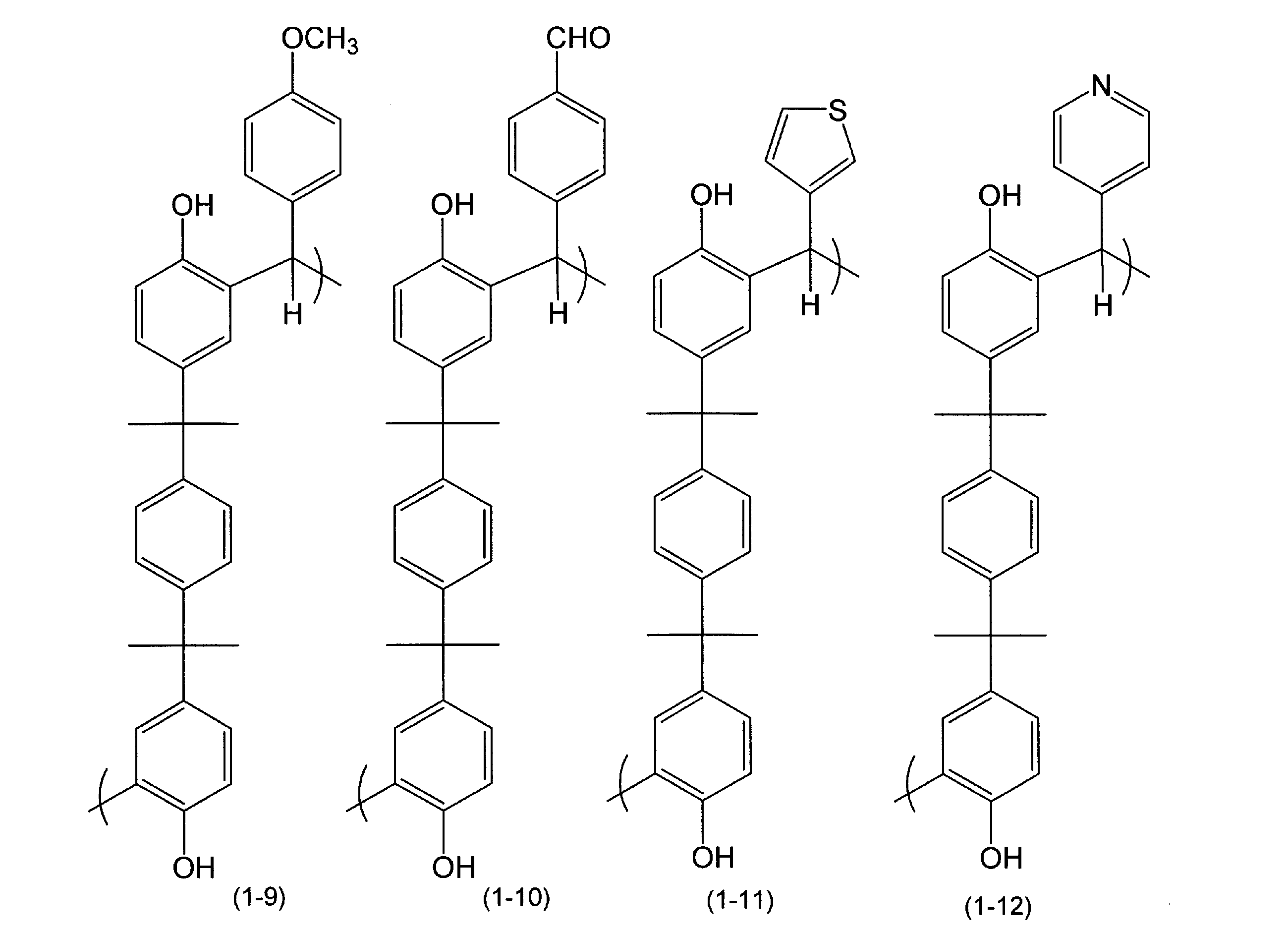
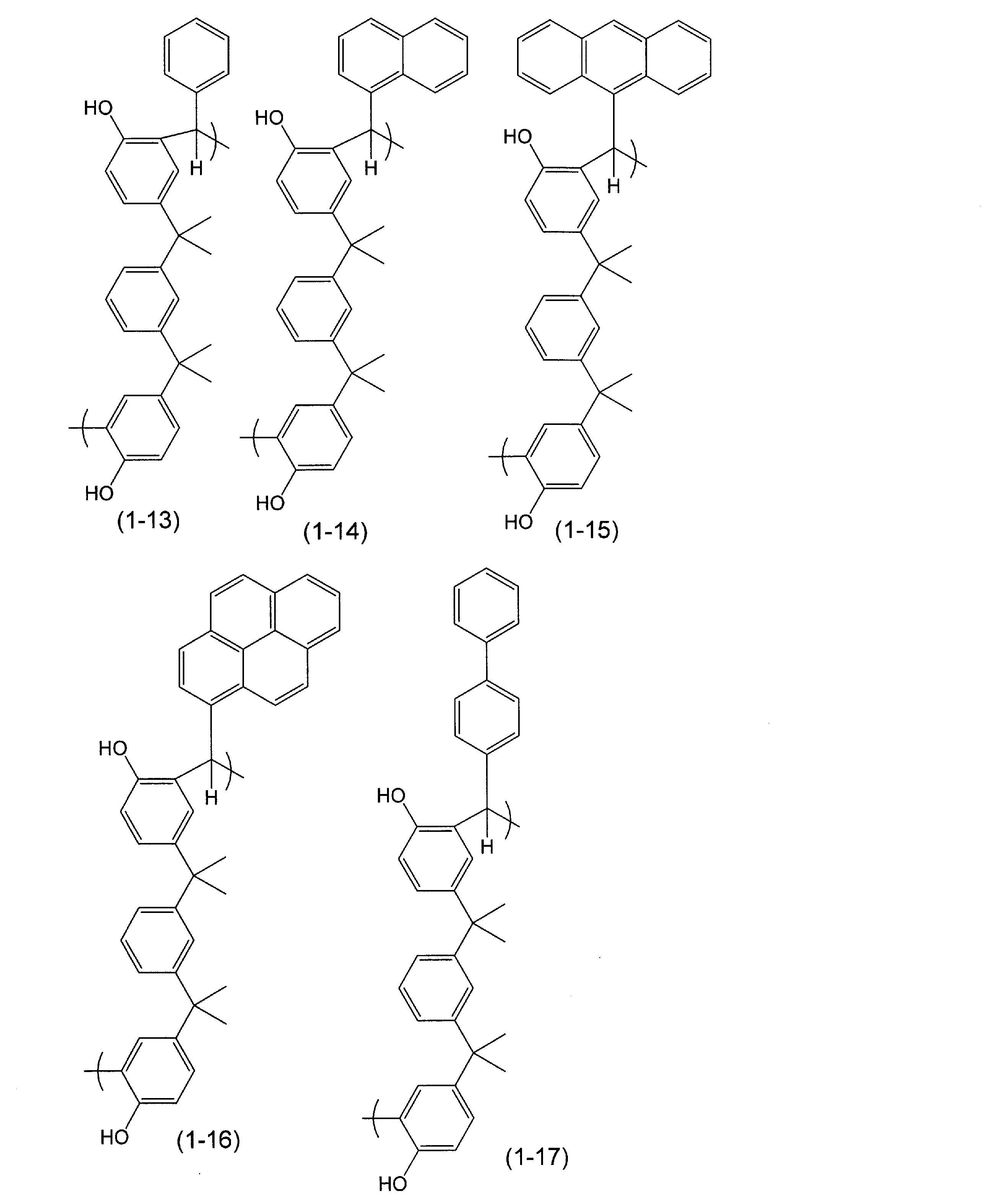
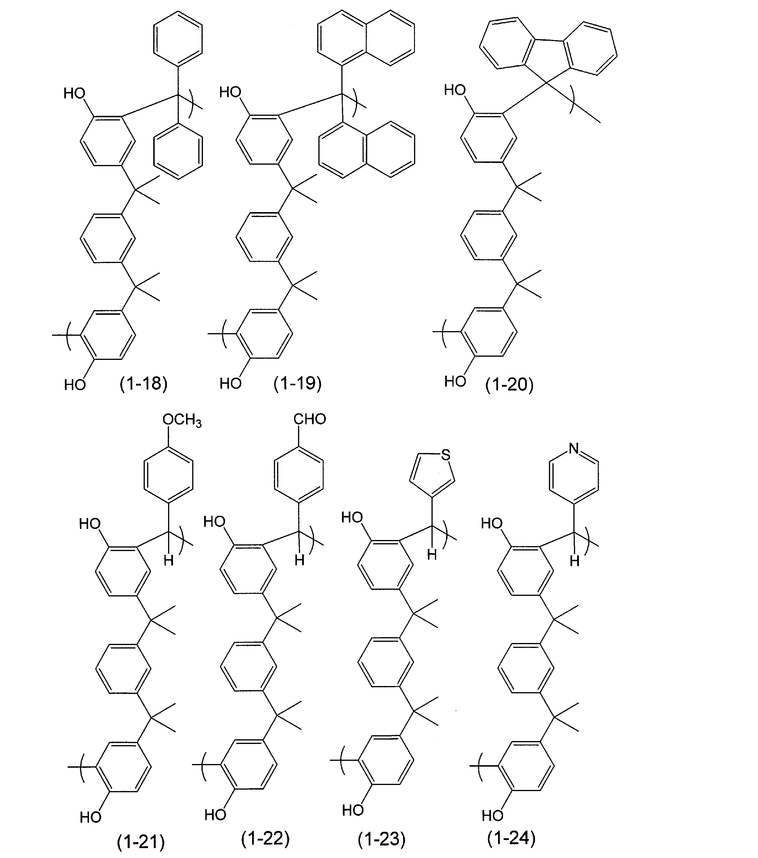
- Examples of the structural unit of the polymer having a repeating structural unit represented by the above formula (1a) contained in the resist underlayer film forming composition of the present invention are represented by the following formulas (1-1) to (1-24).
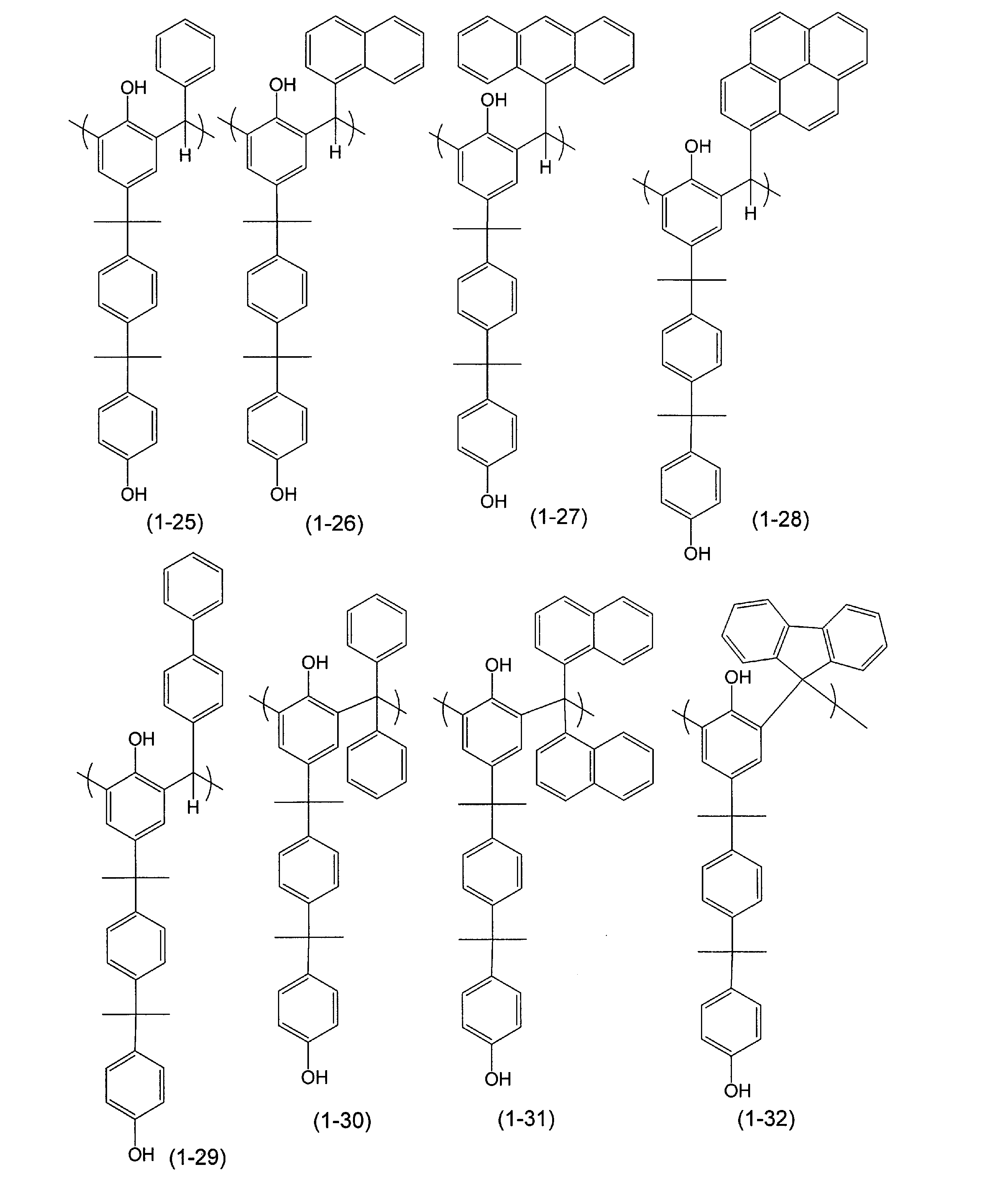
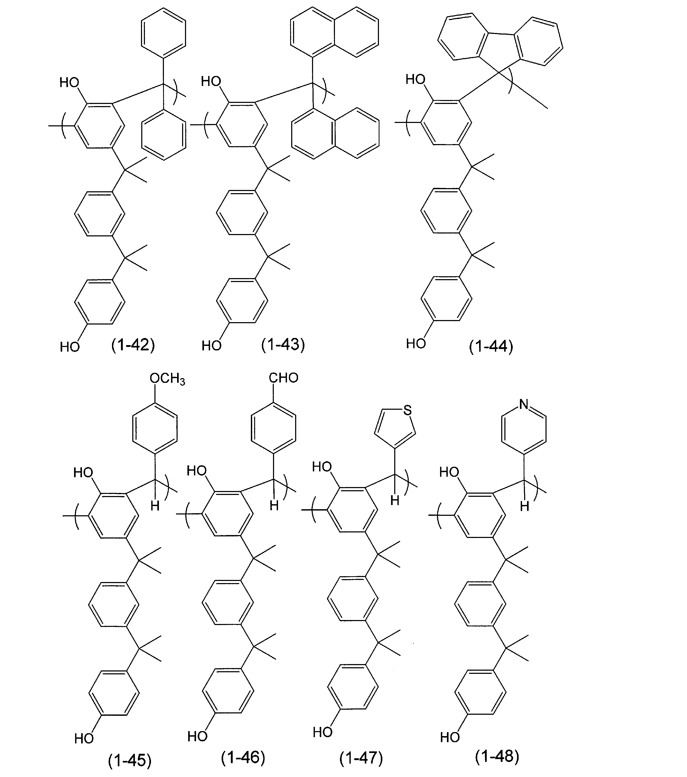
- Examples of the structural unit of the polymer having the repeating structural unit represented by the above formula (1b) include the structural units represented by the following formulas (1-25) to (1-48). It is done.
- the weight average molecular weight of the polymer contained in the resist underlayer film forming composition of the present invention is, for example, 1000 to 50000 in terms of standard polystyrene.
- the polymer is synthesized by polymerizing a bisphenol compound having two hydroxyphenyl groups and an aromatic aldehyde or aromatic ketone in the presence of an acid catalyst such as a sulfonic acid compound.
- an acid catalyst such as a sulfonic acid compound.
- the bisphenol compound include 1,3-bis [2- (4-hydroxyphenyl) -2-propyl] benzene and 1,4-bis [2- (4-hydroxyphenyl) -2-propyl] benzene. It is done.
- aromatic aldehyde examples include benzaldehyde, naphthylaldehyde, anthrylaldehyde, phenanthrylaldehyde, salicylaldehyde, phenylacetaldehyde, 3-phenylpropionaldehyde, tolylaldehyde, (N, N-dimethylamino) benzaldehyde, acetoxybenzaldehyde. , 1-pyrenecarboxaldehyde, and anisaldehyde.
- an aldehyde having a heterocyclic ring such as furfural, pyridinecarboxaldehyde, or thiophenecarboxaldehyde
- the aromatic ketone is a diaryl ketone, and examples thereof include diphenyl ketone, phenyl naphthyl ketone, dinaphthyl ketone, phenyl tolyl ketone, ditolyl ketone, and 9-fluorenone.
- the charging ratio of the bisphenol compound and the aromatic aldehyde or aromatic ketone is, for example, 1: 1 (molar ratio).
- the charge ratio may be selected from 1: 2 (molar ratio).
- the synthesized polymer is represented by the repeating structural unit represented by the formula (1a) and the formula (1b). It has a structural unit that does not correspond to any of the repeating structural units.
- the bisphenol compound is not limited to one type of compound, and two or more types may be used, and the aromatic aldehyde or aromatic ketone is not limited to one type of compound and may be used two or more types.
- 1,3-bis [2- (4-hydroxyphenyl) -2-propyl] benzene and 1,4-bis [2- (4-hydroxyphenyl) -2-propyl] benzene, aromatic aldehydes as bisphenol compounds Benzaldehyde and naphthylaldehyde can be used.
- the resist underlayer film forming composition of the present invention can further contain a crosslinking agent.
- a cross-linkable compound having at least two cross-linking substituents is preferably used.
- examples thereof include melamine compounds, substituted urea compounds and phenolic compounds having a crosslink forming substituent such as a methylol group or a methoxymethyl group.
- Specific examples include compounds such as methoxymethylated glycoluril and methoxymethylated melamine, and examples include tetramethoxymethylglycoluril, tetrabutoxymethylglycoluril, and hexamethoxymethylmelamine.
- examples of the substituted urea compound include tetramethoxymethylurea and tetrabutoxymethylurea.
- examples of phenolic compounds include tetrahydroxymethyl biphenol, tetrahydroxymethyl biphenol, tetramethoxymethyl biphenol (TMOM-BP), and tetramethoxymethyl bisphenol.
- TMOM-BP tetramethoxymethyl biphenol
- TMOM-BP tetramethoxymethyl biphenol
- Examples of such compounds include tris (2,3-epoxypropyl) isocyanurate, 1,4-butanediol diglycidyl ether, 1,2-epoxy-4- (epoxyethyl) cyclohexane, glycerol triglycidyl ether, diethylene glycol Diglycidyl ether, 2,6-diglycidylphenyl glycidyl ether, 1,1,3-tris [p- (2,3-epoxypropoxy) phenyl] propane, 1,2-cyclohexanedicarboxylic acid diglycidyl ester, 4,4 '-Methylenebis (N, N-diglycidylaniline), 3,4-epoxycyclohexylmethyl-3,4-epoxycyclohexanecarboxylate, trimethylolethane triglycidyl ether, bisphenol-A-diglycidyl ether, Epolide [registered trademark] GT-401
- epoxy resins examples include YH-434 and YH-434L (manufactured by Toto Kasei Co., Ltd.).
- crosslinking agent a compound having at least two blocked isocyanate groups can also be used. Examples of such compounds include Takenate (registered trademark) B-830 and B-870N manufactured by Mitsui Chemicals, Inc., and VESTANAT (registered trademark) B1358 / 100 manufactured by Evonik Degussa.
- a compound having at least two vinyl ether groups can also be used.
- Examples of such compounds include bis (4- (vinyloxymethyl) cyclohexylmethyl) glutarate, tri (ethylene glycol) divinyl ether, adipic acid divinyl ester, diethylene glycol divinyl ether, 1,2,4-tris (4-vinyl).
- One kind selected from these various crosslinking agents may be added, or two or more kinds may be added in combination.
- the content of the crosslinking agent is, for example, 2% by mass to 60% by mass with respect to the solid content excluding the solvent described later from the resist underlayer film forming composition of the present invention.
- the resist underlayer film forming composition of the present invention can further contain an acidic compound.
- the acidic compound serves as a catalyst for promoting the cross-linking reaction.
- p-toluenesulfonic acid, trifluoromethanesulfonic acid, pyridinium-p-toluenesulfonate, salicylic acid, camphorsulfonic acid, 5-sulfosalicylic acid, 4-chlorobenzenesulfonic acid examples include 4-hydroxybenzenesulfonic acid, benzenedisulfonic acid, 1-naphthalenesulfonic acid, citric acid, benzoic acid, sulfonic acid compounds such as hydroxybenzoic acid, and carboxylic acid compounds, and inorganic acids such as hydrochloric acid, sulfuric acid, nitric acid, and phosphoric acid.
- a thermal acid generator can be contained.
- the thermal acid generator also serves as a catalyst for promoting the crosslinking reaction, and examples thereof include quaternary ammonium salts of trifluoromethanesulfonic acid.
- One kind selected from these acidic compounds and thermal acid generators may be added, or two or more kinds may be added in combination.
- the content ratio of the acidic compound or thermal acid generator is, for example, 0.1% by mass to 20% by mass with respect to the solid content excluding the solvent described later from the resist underlayer film forming composition of the invention.
- the resist underlayer film forming composition of the present invention can further contain a surfactant.
- the surfactant include polyoxyethylene lauryl ether, polyoxyethylene stearyl ether, polyoxyethylene cetyl ether, polyoxyethylene alkyl ethers such as polyoxyethylene oleyl ether, polyoxyethylene octyl phenyl ether, polyoxyethylene Polyoxyethylene alkyl aryl ethers such as ethylene nonylphenyl ether, polyoxyethylene / polyoxypropylene block copolymers, sorbitan monolaurate, sorbitan monopalmitate, sorbitan monostearate, sorbitan monooleate, sorbitan trioleate, sorbitan Sorbitan fatty acid esters such as tristearate, polyoxyethylene sorbitan monolaurate, polyoxyethylene Nonionic surfactants such as polyoxyethylene sorbitan fatty acid esters such as rubitan monopalmitate, polyoxyethylene sorbitan monoste
- One kind selected from these surfactants may be added, or two or more kinds may be added in combination.
- the content rate of the said surfactant is 0.01 mass% thru
- the resist underlayer film forming composition of the present invention can be prepared by dissolving each of the above components in an appropriate solvent, and is used in a uniform solution state.
- solvents include ethylene glycol monomethyl ether, ethylene glycol monoethyl ether, diethylene glycol monomethyl ether, diethylene glycol monoethyl ether, propylene glycol, propylene glycol monomethyl ether, propylene glycol monopropyl ether, propylene glycol monomethyl ether acetate, propylene glycol.
- the step of applying and baking the resist underlayer film forming composition of the present invention on a surface having a step, a recess and / or a protrusion includes a substrate having a surface having a step, a recess and / or a protrusion (for example, wiring, other structure).
- a silicon wafer on which a body is formed, and the silicon wafer may be coated with a silicon oxide film, a silicon nitride film, a silicon oxynitride film, or a metal film such as aluminum or tungsten).
- the composition is applied by an appropriate application method such as, and then baked using a heating means such as a hot plate. Baking conditions are appropriately selected from the range of a baking temperature of 100 ° C. to 400 ° C. and a baking time of 0.3 minutes to 10 minutes.
- An organopolysiloxane film is formed as a second resist underlayer film on the first resist underlayer film formed by the above process, and a resist pattern is formed thereon.
- a mask reticle
- the exposure source for example, g-line, i-line, KrF excimer laser, ArF excimer laser, EUV, or electron beam can be used.
- post-exposure heating Post ExposureEBake is performed as necessary.
- a developer for example, an aqueous 2.38 mass% tetramethylammonium hydroxide solution
- a rinse solution or pure water to remove the used developer.
- the resist pattern is dried and post-baked in order to improve adhesion to the base.
- the etching process performed after forming the resist pattern is performed by dry etching.
- the etching gas used for dry etching include CHF 3 , CF 4 , and C 2 F 6 for the second resist underlayer film (organopolysiloxane film).
- the resist underlayer film forming composition of the present invention For the formed first resist underlayer film, for example, O 2 , N 2 O, NO 2 can be mentioned, and for the surface having a step or a concave and / or a convex, for example, CHF 3 , CF 4 , C 2 F 6 is mentioned. Further, argon, nitrogen or carbon dioxide can be mixed with these gases.
- the weight average molecular weight and polydispersity shown in the following Synthesis Example 1 and Synthesis Example 2 and Comparative Synthesis Example 1 and Comparative Synthesis Example 2 are measured by gel permeation chromatography (hereinafter abbreviated as GPC in this specification). based on.
- GPC gel permeation chromatography
- a GPC device manufactured by Tosoh Corporation is used, and the measurement conditions are as follows.
- Solvent tetrahydrofuran (THF)
- Flow rate 0.35 mL / min Standard sample: Polystyrene (Tosoh Corporation)
- BPP-Py had a weight average molecular weight Mw of 2,900 and a polydispersity Mw / Mn of 2.10.
- Example 1 20 g of the polymer obtained in Synthesis Example 1 was mixed with 0.06 g of Megafac R-30-N (manufactured by DIC Corporation) as a surfactant and dissolved in 24 g of propylene glycol monomethyl ether and 66 g of propylene glycol monomethyl ether acetate. It was set as the solution. Then, it filtered using the polyethylene micro filter with a hole diameter of 0.10 micrometer, and also filtered using the polyethylene micro filter with the hole diameter of 0.05 micrometer, and prepared the resist underlayer film forming composition used for a lithography process.
- Megafac R-30-N manufactured by DIC Corporation
- Example 2 20 g of the polymer obtained in Synthesis Example 2 is mixed with 0.06 g of Megafac R-30-N (manufactured by DIC Corporation) as a surfactant and dissolved in 24 g of propylene glycol monomethyl ether and 66 g of propylene glycol monomethyl ether acetate. It was set as the solution. Then, it filtered using the polyethylene micro filter with a hole diameter of 0.10 micrometer, and also filtered using the polyethylene micro filter with the hole diameter of 0.05 micrometer, and prepared the resist underlayer film forming composition used for a lithography process.
- Megafac R-30-N manufactured by DIC Corporation
- Comparative Example 1 20 g of the polymer obtained in Comparative Synthesis Example 1 was mixed with 0.06 g of Megafac R-30 (manufactured by DIC Corporation) as a surfactant and dissolved in 24 g of propylene glycol monomethyl ether and 66 g of propylene glycol monomethyl ether acetate. It was. Then, it filtered using the polyethylene micro filter with a hole diameter of 0.10 micrometer, and also filtered using the polyethylene micro filter with the hole diameter of 0.05 micrometer, and prepared the resist underlayer film forming composition used for a lithography process.
- Megafac R-30 manufactured by DIC Corporation
- Comparative Example 2 0.06 g of Megafac R-30 (manufactured by DIC Corporation) as a surfactant was mixed with 20 g of the polymer obtained in Comparative Synthesis Example 2, and dissolved in 80 g of propylene glycol monomethyl ether acetate to obtain a solution. Then, it filtered using the polyethylene micro filter with a hole diameter of 0.10 micrometer, and also filtered using the polyethylene micro filter with the hole diameter of 0.05 micrometer, and prepared the resist underlayer film forming composition used for a lithography process.
- Megafac R-30 manufactured by DIC Corporation
- the etcher and etching gas used for the measurement of the dry etching rate are as follows.
- Etching gas: CF 4 The resist underlayer film forming compositions prepared in Example 1 and Example 2 and Comparative Example 1 and Comparative Example 2 were each applied onto a silicon wafer using a spin coater. Baking was performed at 400 ° C. for 2 minutes on a hot plate to form a resist underlayer film (film thickness: 0.25 ⁇ m). Using CF 4 gas as an etching gas, the dry etching rate of these resist underlayer films was measured.
- the film thickness decreased per unit time (1 minute) of the resist underlayer film formed from the resist underlayer film forming composition prepared in Example 1 and Example 2 and Comparative Example 1 and Comparative Example 2 was defined as the dry etching rate.
- the calculated results are shown in Table 1. The smaller the dry etching rate, the higher the etching resistance against CF 4 gas.
- the resist underlayer film forming compositions prepared in Example 1, Example 2 and Comparative Example 2 were each applied onto a hole wafer using a spin coater. Baking was carried out on a hot plate at 400 ° C. for 2 minutes to form a resist underlayer film (thickness of the hole pattern non-formed portion 0.25 ⁇ m). As the hole wafer, a wafer on which a hole pattern with a diameter of 100 nm and a height of 400 nm was formed was used. The resist underlayer film forming composition prepared in Example 1 and Example 2 was applied as described above, and the cross section of each hole wafer after baking was observed with a scanning electron microscope (SEM). From the cross-sectional SEM photograph shown in FIG.
- SEM scanning electron microscope
Landscapes
- Chemical & Material Sciences (AREA)
- Engineering & Computer Science (AREA)
- Organic Chemistry (AREA)
- General Physics & Mathematics (AREA)
- Physics & Mathematics (AREA)
- Structural Engineering (AREA)
- Architecture (AREA)
- Polymers & Plastics (AREA)
- Health & Medical Sciences (AREA)
- Medicinal Chemistry (AREA)
- Chemical Kinetics & Catalysis (AREA)
- Life Sciences & Earth Sciences (AREA)
- Materials Engineering (AREA)
- Wood Science & Technology (AREA)
- Materials For Photolithography (AREA)
- Phenolic Resins Or Amino Resins (AREA)
- Photosensitive Polymer And Photoresist Processing (AREA)
Abstract
Description
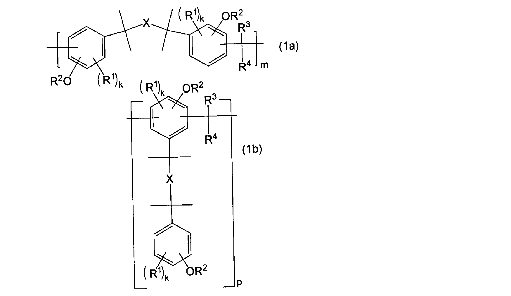
で表される繰り返し構造単位を有するポリマー及び溶剤を含むレジスト下層膜形成組成物である。



前記架橋剤としては、また、少なくとも二つのエポキシ基を有する化合物を用いることもできる。このような化合物として、例えば、トリス(2,3-エポキシプロピル)イソシアヌレート、1,4-ブタンジオールジグリシジルエーテル、1,2-エポキシ-4-(エポキシエチル)シクロヘキサン、グリセロールトリグリシジルエーテル、ジエチレングリコールジグリシジルエーテル、2,6-ジグリシジルフェニルグリシジルエーテル、1,1,3-トリス[p-(2,3-エポキシプロポキシ)フェニル]プロパン、1,2-シクロヘキサンジカルボン酸ジグリシジルエステル、4,4’-メチレンビス(N,N-ジグリシジルアニリン)、3,4-エポキシシクロヘキシルメチル-3,4-エポキシシクロヘキサンカルボキシレート、トリメチロールエタントリグリシジルエーテル、ビスフェノール-A-ジグリシジルエーテル、(株)ダイセル製のエポリード〔登録商標〕GT-401、同GT-403、同GT-301、同GT-302、セロキサイド〔登録商標〕2021、同3000、三菱化学(株)製の1001、1002、1003、1004、1007、1009、1010、828、807、152、154、180S75、871、872、日本化薬(株)製のEPPN201、同202、EOCN-102、同103S、同104S、同1020、同1025、同1027、ナガセケムテックス(株)製のデナコール〔登録商標〕EX-252、同EX-611、同EX-612、同EX-614、同EX-622、同EX-411、同EX-512、同EX-522、同EX-421、同EX-313、同EX-314、同EX-321、BASFジャパン(株)製のCY175、CY177、CY179、CY182、CY184、CY192、DIC(株)製のエピクロン200、同400、同7015、同835LV、同850CRPを挙げることができる。前記少なくとも二つのエポキシ基を有する化合物としては、また、アミノ基を有するエポキシ樹脂を使用することもできる。このようなエポキシ樹脂として、例えば、YH-434、YH-434L(東都化成(株)製)が挙げられる。
前記架橋剤としては、また、少なくとも2つのブロックイソシアネート基を有する化合物を使用することもできる。このような化合物として、例えば、三井化学(株)製のタケネート〔登録商標〕B-830、同B-870N、エボニック デグサ社製のVESTANAT〔登録商標〕B1358/100が挙げられる。
前記架橋剤としては、また、少なくとも2つのビニルエーテル基を有する化合物を使用することもできる。このような化合物として、例えば、ビス(4-(ビニルオキシメチル)シクロヘキシルメチル)グルタレート、トリ(エチレングリコール)ジビニルエーテル、アジピン酸ジビニルエステル、ジエチレングリコールジビニルエーテル、1,2,4-トリス(4-ビニルオキシブチル)トリメリテート、1,3,5-トリス(4-ビニルオキシブチル)トリメリテート、ビス(4-(ビニルオキシ)ブチル)テレフタレート、ビス(4-(ビニルオキシ)ブチル)イソフタレート、エチレングリコールジビニルエーテル、1,4-ブタンジオールジビニルエーテル、テトラメチレングリコールジビニルエーテル、テトラエチレングリコールジビニルエーテル、ネオペンチルグリコールジビニルエーテル、トリメチロールプロパントリビニルエーテル、トリメチロールエタントリビニルエーテル、ヘキサンジオールジビニルエーテル、1,4-シクロヘキサンジオールジビニルエーテル、テトラエチレングリコールジビニルエーテル、ペンタエリスリトールジビニルエーテル、ペンタエリスリトールトリビニルエーテル及びシクロヘキサンジメタノールジビニルエーテルを挙げることができる。これらの各種架橋剤から選択された1種類を添加してもよいし、2種以上を組合せて添加することもできる。
前記架橋剤の含有割合は、本発明のレジスト下層膜形成組成物から後述する溶剤を除いた固形分に対して、例えば2質量%乃至60質量%である。
GPCカラム:TSKgel SuperMultipore〔登録商標〕Hz-N(東ソー(株))
カラム温度:40℃
溶媒:テトラヒドロフラン(THF)
流量:0.35mL/分
標準試料:ポリスチレン(東ソー(株))
窒素下、300mL四口フラスコに、1,3-ビス[2-(4-ヒドロキシフェニル)-2-プロピル]ベンゼン(10.00g、0.0289mol、東京化成工業(株)製)、1-ピレンカルボキシアルデヒド(6.646g、0.0289mol、アルドリッチ社製)及びメタンスルホン酸(0.5548g、0.0058mol、東京化成工業(株)製)を加え、さらにプロピレングリコールモノメチルエーテル(7.74g、関東化学(株)製)及びプロピレングリコールモノメチルエーテルアセテート(18.06g、関東化学(株)製)を仕込んだ。前記四口フラスコ内の混合物を撹拌し、120℃まで昇温して溶解させ、重合を開始した。24時間後室温まで放冷し、メタノール(500g、関東化学(株)製)中へ再沈殿させた。得られた沈殿物をろ過し、減圧乾燥機で50℃、10時間乾燥し、目的とするポリマー(以下、本明細書ではBPM-Pyと略称する。)10.82gを得た。BPM-Pyの、GPCによるポリスチレン換算で測定される重量平均分子量Mwは6,300、多分散度Mw/Mn(Mnは数平均分子量)1.90であった。
窒素下、300mL四口フラスコに、1,4-ビス[2-(4-ヒドロキシフェニル)-2-プロピル]ベンゼン(10.00g、0.0289mol、東京化成工業(株)製)、1-ピレンカルボキシアルデヒド(6.646g、0.0289mol、アルドリッチ社製)及びメタンスルホン酸(0.5548g、0.0058mol、東京化成工業(株)製)を加え、さらにプロピレングリコールモノメチルエーテル(7.74g、関東化学(株)製)及びプロピレングリコールモノメチルエーテルアセテート(18.06g、関東化学(株)製)を仕込んだ。前記四口フラスコ内の混合物を撹拌し、120℃まで昇温して溶解させ、重合を開始した。24時間後室温まで放冷し、メタノール(500g、関東化学(株)製)中へ再沈殿させた。得られた沈殿物をろ過し、減圧乾燥機で50℃、10時間乾燥し、目的とするポリマー(以下、本明細書ではBPP-Pyと略称する。)9.16gを得た。BPP-Pyの、GPCによるポリスチレン換算で測定される重量平均分子量Mwは2,900、多分散度Mw/Mnは2.10であった。
窒素下、1000mL四口フラスコに2,2'-ビフェノール(70.00g、0.3759mol、東京化成工業(株)製)、1-ピレンカルボキシアルデヒド(86.559g、0.3759mol、アルドリッチ社製)及びメタンスルホン酸(10.8389g、0.1126mol、東京化成工業(株)製)を加え、さらにプロピレングリコールモノメチルエーテル(167.40g、関東化学(株)製)を仕込んだ。前記四口フラスコ内の混合物を撹拌し、120℃まで昇温して溶解させ、重合を開始した。24時間後室温まで放冷し、メタノール(3000g、関東化学(株)製)中へ再沈殿させた。得られた沈殿物をろ過し、減圧乾燥機で50℃、10時間乾燥し、下記式(3)で表される構造単位を有するポリマー(以下、本明細書では2,2'-BPOH-Pyと略称する。)84.1gを得た。2,2'-BPOH-Pyの、GPCによるポリスチレン換算で測定される重量平均分子量Mwは1400、多分散度Mw/Mnは1.49であった。

窒素下、100mL四口フラスコにカルバゾール(6.69g、0.040mol、東京化成工業(株)製)、9-フルオレノン(7.28g、0.040mol、東京化成工業(株)製)及びパラトルエンスルホン酸一水和物(0.76g、0.0040mol、東京化成工業(株)製)を加え、さらに1,4-ジオキサン(6.69g、関東化学(株)製)を仕込んだ。前記四口フラスコ内の混合物を撹拌し、100℃まで昇温して溶解させ、重合を開始した。24時間後60℃まで放冷し、クロロホルム(34g、関東化学(株)製)を加え希釈し、メタノール(168g、関東化学(株)製)中へ再沈殿させた。得られた沈殿物をろ過し、減圧乾燥機で80℃、24時間乾燥し、目的とする下記式(4)で表される構造単位を有するポリマー(以下、本明細書ではPCzFLと略称する。)9.37gを得た。PCzFLの、GPCによるポリスチレン換算で測定される重量平均分子量Mwは2800、多分散度Mw/Mnは1.77であった。

合成例1で得たポリマー20gに、界面活性剤としてメガファックR-30-N(DIC(株)製)0.06gを混合し、プロピレングリコールモノメチルエーテル24g及びプロピレングリコールモノメチルエーテルアセテート66gに溶解させ溶液とした。その後、孔径0.10μmのポリエチレン製ミクロフィルターを用いて濾過し、更に、孔径0.05μmのポリエチレン製ミクロフィルターを用いて濾過して、リソグラフィープロセスに用いるレジスト下層膜形成組成物を調製した。
合成例2で得たポリマー20gに、界面活性剤としてメガファックR-30-N(DIC(株)製)0.06gを混合し、プロピレングリコールモノメチルエーテル24g及びプロピレングリコールモノメチルエーテルアセテート66gに溶解させ溶液とした。その後、孔径0.10μmのポリエチレン製ミクロフィルターを用いて濾過し、更に、孔径0.05μmのポリエチレン製ミクロフィルターを用いて濾過して、リソグラフィープロセスに用いるレジスト下層膜形成組成物を調製した。
比較合成例1で得たポリマー20gに、界面活性剤としてメガファックR-30(DIC(株)製)0.06gを混合し、プロピレングリコールモノメチルエーテル24g及びプロピレングリコールモノメチルエーテルアセテート66gに溶解させ溶液とした。その後、孔径0.10μmのポリエチレン製ミクロフィルターを用いて濾過し、更に、孔径0.05μmのポリエチレン製ミクロフィルターを用いて濾過して、リソグラフィープロセスに用いるレジスト下層膜形成組成物を調製した。
比較合成例2で得たポリマー20gに、界面活性剤としてメガファックR-30(DIC(株)製)0.06gを混合し、プロピレングリコールモノメチルエーテルアセテート80gに溶解させ溶液とした。その後、孔径0.10μmのポリエチレン製ミクロフィルターを用いて濾過し、更に、孔径0.05μmのポリエチレン製ミクロフィルターを用いて濾過して、リソグラフィープロセスに用いるレジスト下層膜形成組成物を調製した。
実施例1及び実施例2並びに比較例1及び比較例2で調製したレジスト下層膜形成組成物を、それぞれスピンコーターを用いてシリコンウェハー上に塗布した。ホットプレート上で400℃,2分間ベークし、レジスト下層膜(膜厚0.25μm)を形成した。このレジスト下層膜を、レジストに使用する溶剤である乳酸エチル、プロピレングリコールモノメチルエーテル、プロピレングリコールモノメチルエーテルアセテート及びシクロヘキサノンに浸漬し、それらの溶剤に不溶であることを確認した。
ドライエッチング速度の測定に用いたエッチャー及びエッチングガスは以下のものである。
エッチャー:ES401(日本サイエンティフィック(株)製)
エッチングガス:CF4
実施例1及び実施例2並びに比較例1及び比較例2で調製したレジスト下層膜形成組成物を、それぞれスピンコーターを用いてシリコンウェハー上に塗布した。ホットプレート上で400℃,2分間ベークし、レジスト下層膜(膜厚0.25μm)を形成した。エッチングガスとしてCF4ガスを使用して、それらのレジスト下層膜のドライエッチング速度を測定した。実施例1及び実施例2並びに比較例1及び比較例2で調製したレジスト下層膜形成組成物から形成したレジスト下層膜の、単位時間(1分間)あたりに減少した膜厚を、ドライエッチング速度として算出した結果を表1に示す。ドライエッチング速度が小さいほど、CF4ガスに対する耐エッチング性が高いことを示す。

実施例1及び実施例2並びに比較例2で調製したレジスト下層膜形成組成物を、それぞれスピンコーターを用いてホールウェハー上に塗布した。ホットプレート上で400℃,2分間ベークし、レジスト下層膜(ホールパターン未形成部の膜厚0.25μm)を形成した。前記ホールウェハーとして、直径100nm、高さ400nmのホールパターンが形成されたウェハーを用いた。実施例1及び実施例2で調製したレジスト下層膜形成組成物を、それぞれ上述のように塗布し、ベークした後の各ホールウェハーの断面を走査型電子顕微鏡(SEM)で観察した図1及び図2に示す断面SEM写真から、ホール内部まで十分にレジスト下層膜で充填されていることが分かった。一方、比較例2で調製したレジスト下層膜形成組成物を、上述のように塗布し、ベークした後のホールウェハーの断面を走査型電子顕微鏡で観察した図3に示す断面SEM写真から、ホール内部に部分的に空洞が存在していることが分かった。
実施例1及び実施例2並びに比較例1及び比較例2で調製したレジスト下層膜形成組成物と、2-ヒドロキシイソ酪酸メチルを、質量比(9:1)で混合し、混合後の析出物の有無を確認した。表2にその結果を示す。実施例1及び実施例2で調製したレジスト下層膜形成組成物は、2-ヒドロキシイソ酪酸メチルに溶解することを確認した。一方、比較例1及び比較例2で調製したレジスト下層膜形成組成物は、2-ヒドロキシイソ酪酸メチルと混合させた結果、該レジスト下層膜形成組成物の析出物が生成した。

Claims (6)
- 下記式(1a)及び/又は式(1b):

で表される繰り返し構造単位を有するポリマー及び溶剤を含むレジスト下層膜形成組成物。 - 前記ポリマーは、少なくとも1種のビスフェノール化合物と少なくとも1種の芳香族アルデヒド又は芳香族ケトンとの重合反応物である請求項1に記載のレジスト下層膜形成組成物。
- 前記R3が表す芳香族炭化水素基はフェニル基、ナフチル基、アントリル基又はピレニル基である請求項1に記載のレジスト下層膜形成組成物。
- 架橋剤、酸性化合物、熱酸発生剤及び界面活性剤のうち少なくとも1つをさらに含有する請求項1乃至請求項3のいずれか一項に記載のレジスト下層膜形成組成物。
- 請求項1乃至請求項4のいずれか一項に記載のレジスト下層膜形成組成物を、段差、凹部及び/又は凸部を有する基板の表面に塗布しベークすることにより第1のレジスト下層膜を形成する工程、前記第1のレジスト下層膜上にオルガノポリシロキサン膜を第2のレジスト下層膜として形成する工程、前記第2のレジスト下層膜上にレジストパターンを形成する工程、前記レジストパターンをマスクとして前記第2のレジスト下層膜をエッチングする工程、エッチング後の前記第2のレジスト下層膜のパターンをマスクとして前記第1のレジスト下層膜をエッチングする工程、及びエッチング後の前記第1のレジスト下層膜のパターンをマスクとして前記段差、凹部及び/又は凸部を有する表面をエッチングする工程を含む半導体装置の製造方法。
- 前記第1のレジスト下層膜を形成する工程及び/又は前記第2のレジスト下層膜を形成する工程において、2-ヒドロキシイソ酪酸メチルを用いた、前記段差、凹部及び/又は凸部を有する基板に対するプリウェット処理、エッジリンス及びバックリンスをさらに行う、請求項5に記載の半導体装置の製造方法。
Priority Applications (4)
| Application Number | Priority Date | Filing Date | Title |
|---|---|---|---|
| US16/302,603 US10585353B2 (en) | 2016-05-20 | 2017-05-02 | Resist underlayer film forming composition |
| CN201780030002.7A CN109154778B (zh) | 2016-05-20 | 2017-05-02 | 抗蚀剂下层膜形成用组合物 |
| KR1020187031994A KR102391745B1 (ko) | 2016-05-20 | 2017-05-02 | 레지스트 하층막 형성 조성물 |
| JP2018518218A JP6901704B2 (ja) | 2016-05-20 | 2017-05-02 | レジスト下層膜形成組成物 |
Applications Claiming Priority (2)
| Application Number | Priority Date | Filing Date | Title |
|---|---|---|---|
| JP2016-101585 | 2016-05-20 | ||
| JP2016101585 | 2016-05-20 |
Publications (1)
| Publication Number | Publication Date |
|---|---|
| WO2017199768A1 true WO2017199768A1 (ja) | 2017-11-23 |
Family
ID=60325363
Family Applications (1)
| Application Number | Title | Priority Date | Filing Date |
|---|---|---|---|
| PCT/JP2017/017272 Ceased WO2017199768A1 (ja) | 2016-05-20 | 2017-05-02 | レジスト下層膜形成組成物 |
Country Status (6)
| Country | Link |
|---|---|
| US (1) | US10585353B2 (ja) |
| JP (1) | JP6901704B2 (ja) |
| KR (1) | KR102391745B1 (ja) |
| CN (1) | CN109154778B (ja) |
| TW (1) | TWI727044B (ja) |
| WO (1) | WO2017199768A1 (ja) |
Cited By (2)
| Publication number | Priority date | Publication date | Assignee | Title |
|---|---|---|---|---|
| WO2020017626A1 (ja) * | 2018-07-20 | 2020-01-23 | 日産化学株式会社 | レジスト下層膜形成組成物 |
| WO2025205630A1 (ja) * | 2024-03-27 | 2025-10-02 | 日産化学株式会社 | レジスト下層膜形成用組成物、レジスト下層膜、レジストパターンの形成方法、及び半導体装置の製造方法 |
Families Citing this family (3)
| Publication number | Priority date | Publication date | Assignee | Title |
|---|---|---|---|---|
| US11545354B2 (en) | 2020-07-22 | 2023-01-03 | Applied Materials, Inc. | Molecular layer deposition method and system |
| US11972940B2 (en) | 2022-04-18 | 2024-04-30 | Applied Materials, Inc. | Area selective carbon-based film deposition |
| US12577667B2 (en) | 2024-03-29 | 2026-03-17 | Applied Materials, Inc. | Cyclic alkyl amino carbene (CAAC) deposition by transmetallation |
Citations (2)
| Publication number | Priority date | Publication date | Assignee | Title |
|---|---|---|---|---|
| WO2014024836A1 (ja) * | 2012-08-10 | 2014-02-13 | 日産化学工業株式会社 | レジスト下層膜形成組成物 |
| JP2014528095A (ja) * | 2011-09-07 | 2014-10-23 | マイクロケム コーポレイション | 低表面エネルギー基板上にレリーフパターンを製作するためのエポキシ配合物及び方法 |
Family Cites Families (10)
| Publication number | Priority date | Publication date | Assignee | Title |
|---|---|---|---|---|
| JPS6210645A (ja) * | 1985-07-09 | 1987-01-19 | Kanto Kagaku Kk | ポジ型フオトレジスト組成物 |
| JP2001330960A (ja) * | 2000-05-24 | 2001-11-30 | Hitachi Chem Co Ltd | ポジ型化学増幅系感光性樹脂組成物及びレジスト像の製造法 |
| TW591341B (en) * | 2001-09-26 | 2004-06-11 | Shipley Co Llc | Coating compositions for use with an overcoated photoresist |
| SG176777A1 (en) | 2009-06-19 | 2012-01-30 | Nissan Chemical Ind Ltd | Carbazole novolak resin |
| WO2012050064A1 (ja) * | 2010-10-14 | 2012-04-19 | 日産化学工業株式会社 | ポリエーテル構造を含有する樹脂を含むリソグラフィー用レジスト下層膜形成組成物 |
| JP5598489B2 (ja) * | 2011-03-28 | 2014-10-01 | 信越化学工業株式会社 | ビフェニル誘導体、レジスト下層膜材料、レジスト下層膜形成方法及びパターン形成方法 |
| WO2013146670A1 (ja) | 2012-03-27 | 2013-10-03 | 日産化学工業株式会社 | フェニルインドール含有ノボラック樹脂を含むレジスト下層膜形成組成物 |
| JP5894106B2 (ja) | 2012-06-18 | 2016-03-23 | 信越化学工業株式会社 | レジスト下層膜形成用化合物、これを用いたレジスト下層膜材料、レジスト下層膜形成方法、パターン形成方法 |
| JP6196190B2 (ja) * | 2014-07-08 | 2017-09-13 | 信越化学工業株式会社 | 多層膜形成方法及びパターン形成方法 |
| JP6378146B2 (ja) * | 2014-10-16 | 2018-08-22 | 信越化学工業株式会社 | 多層膜形成方法及びパターン形成方法 |
-
2017
- 2017-05-02 CN CN201780030002.7A patent/CN109154778B/zh active Active
- 2017-05-02 JP JP2018518218A patent/JP6901704B2/ja active Active
- 2017-05-02 WO PCT/JP2017/017272 patent/WO2017199768A1/ja not_active Ceased
- 2017-05-02 KR KR1020187031994A patent/KR102391745B1/ko active Active
- 2017-05-02 US US16/302,603 patent/US10585353B2/en active Active
- 2017-05-16 TW TW106116130A patent/TWI727044B/zh active
Patent Citations (2)
| Publication number | Priority date | Publication date | Assignee | Title |
|---|---|---|---|---|
| JP2014528095A (ja) * | 2011-09-07 | 2014-10-23 | マイクロケム コーポレイション | 低表面エネルギー基板上にレリーフパターンを製作するためのエポキシ配合物及び方法 |
| WO2014024836A1 (ja) * | 2012-08-10 | 2014-02-13 | 日産化学工業株式会社 | レジスト下層膜形成組成物 |
Cited By (3)
| Publication number | Priority date | Publication date | Assignee | Title |
|---|---|---|---|---|
| WO2020017626A1 (ja) * | 2018-07-20 | 2020-01-23 | 日産化学株式会社 | レジスト下層膜形成組成物 |
| CN112470076A (zh) * | 2018-07-20 | 2021-03-09 | 日产化学株式会社 | 抗蚀剂下层膜形成用组合物 |
| WO2025205630A1 (ja) * | 2024-03-27 | 2025-10-02 | 日産化学株式会社 | レジスト下層膜形成用組成物、レジスト下層膜、レジストパターンの形成方法、及び半導体装置の製造方法 |
Also Published As
| Publication number | Publication date |
|---|---|
| JP6901704B2 (ja) | 2021-07-14 |
| TWI727044B (zh) | 2021-05-11 |
| CN109154778A (zh) | 2019-01-04 |
| CN109154778B (zh) | 2022-08-02 |
| US10585353B2 (en) | 2020-03-10 |
| TW201819443A (zh) | 2018-06-01 |
| KR20190013730A (ko) | 2019-02-11 |
| US20190294046A1 (en) | 2019-09-26 |
| JPWO2017199768A1 (ja) | 2019-03-22 |
| KR102391745B1 (ko) | 2022-04-28 |
Similar Documents
| Publication | Publication Date | Title |
|---|---|---|
| JP6191831B2 (ja) | レジスト下層膜形成組成物 | |
| JP6327481B2 (ja) | レジスト下層膜形成組成物 | |
| JP6471873B2 (ja) | レジスト下層膜形成組成物 | |
| US8962234B2 (en) | Resist underlayer film forming composition and method for forming resist pattern using the same | |
| CN110546569B (zh) | 抗蚀剂下层膜形成用组合物 | |
| TW201319755A (zh) | 具有縮合系聚合物之euv微影用光阻下層膜形成組成物 | |
| KR20170081166A (ko) | 아릴렌기를 갖는 폴리머를 포함하는 레지스트 하층막 형성 조성물 | |
| JP6901704B2 (ja) | レジスト下層膜形成組成物 | |
| CN108713164B (zh) | 抗蚀剂下层膜形成用组合物及使用了该组合物的抗蚀剂图案的形成方法 | |
| JP2015145944A (ja) | レジスト下層膜形成組成物及びそれを用いたレジストパターンの形成方法 |
Legal Events
| Date | Code | Title | Description |
|---|---|---|---|
| ENP | Entry into the national phase |
Ref document number: 2018518218 Country of ref document: JP Kind code of ref document: A |
|
| ENP | Entry into the national phase |
Ref document number: 20187031994 Country of ref document: KR Kind code of ref document: A |
|
| NENP | Non-entry into the national phase |
Ref country code: DE |
|
| 121 | Ep: the epo has been informed by wipo that ep was designated in this application |
Ref document number: 17799194 Country of ref document: EP Kind code of ref document: A1 |
|
| 122 | Ep: pct application non-entry in european phase |
Ref document number: 17799194 Country of ref document: EP Kind code of ref document: A1 |