WO2017199701A1 - モジュール及びセンサ装置 - Google Patents
モジュール及びセンサ装置 Download PDFInfo
- Publication number
- WO2017199701A1 WO2017199701A1 PCT/JP2017/016242 JP2017016242W WO2017199701A1 WO 2017199701 A1 WO2017199701 A1 WO 2017199701A1 JP 2017016242 W JP2017016242 W JP 2017016242W WO 2017199701 A1 WO2017199701 A1 WO 2017199701A1
- Authority
- WO
- WIPO (PCT)
- Prior art keywords
- electronic circuit
- pin header
- pad
- mold body
- module
- Prior art date
- Legal status (The legal status is an assumption and is not a legal conclusion. Google has not performed a legal analysis and makes no representation as to the accuracy of the status listed.)
- Ceased
Links
Images

Classifications
-
- G—PHYSICS
- G01—MEASURING; TESTING
- G01R—MEASURING ELECTRIC VARIABLES; MEASURING MAGNETIC VARIABLES
- G01R33/00—Arrangements or instruments for measuring magnetic variables
- G01R33/02—Measuring direction or magnitude of magnetic fields or magnetic flux
-
- H—ELECTRICITY
- H10—SEMICONDUCTOR DEVICES; ELECTRIC SOLID-STATE DEVICES NOT OTHERWISE PROVIDED FOR
- H10N—ELECTRIC SOLID-STATE DEVICES NOT OTHERWISE PROVIDED FOR
- H10N50/00—Galvanomagnetic devices
- H10N50/80—Constructional details
-
- H—ELECTRICITY
- H10—SEMICONDUCTOR DEVICES; ELECTRIC SOLID-STATE DEVICES NOT OTHERWISE PROVIDED FOR
- H10W—GENERIC PACKAGES, INTERCONNECTIONS, CONNECTORS OR OTHER CONSTRUCTIONAL DETAILS OF DEVICES COVERED BY CLASS H10
- H10W74/00—Encapsulations, e.g. protective coatings
Definitions
- the present invention relates to a module and a sensor device.
- a magnetic sensor element an IC (Integrated Circuit) that is wire-bonded to the magnetic sensor element, amplifies the output of the magnetic sensor element, performs a predetermined process, and outputs the magnetic sensor element; and a magnet that applies a magnetic bias to the magnetic sensor element
- IC Integrated Circuit
- a magnetic sensor element and an IC are arranged in a frame.
- the magnetic sensor module has leads that are wire-bonded to the IC, and the magnetic sensor element, IC, magnet, frame, and leads are sealed with a sealing resin.
- a structure for positioning with a mold Is required for the magnetic sensor module.
- this positioning structure is such that a part of the frame or the like protrudes from the magnetic sensor module, a gap may be formed between the secondary mold body and liquid such as water may enter the interior.
- An object of the present invention is to provide a module and a sensor device that do not require components used only for positioning and can suppress an increase in the number of components.
- a module includes an electronic circuit that performs a predetermined process, a base on which the electronic circuit is disposed, and a pad that is bent at one end and bonded to the pad.
- the pin header used for positioning in the secondary molding with the other end serving as a connector terminal, and the electronic circuit, the substrate and the pin header so that the connector terminal is exposed.
- a primary mold body obtained by resin-sealing the end portion.
- a module and a sensor device that do not require components used only for positioning and suppress an increase in the number of components.
- FIG. 1A and 1B are explanatory views showing a sensor module according to an embodiment, wherein FIG. 1A is a top view and FIG. 1B is a side view.
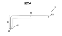
- FIG. 2A is a side view showing a pin header of the sensor module according to the embodiment.
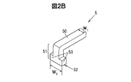
- FIG. 2B is a perspective view showing an anchor portion of the pin header.
- the module according to the embodiment is joined to an electronic circuit that performs a predetermined process, a base body on which the electronic circuit is disposed, and a pad that is bent at one end and provided on the base body, and is connected via the pad.
- FIGS. 1A and 1B are explanatory views showing a sensor module according to an embodiment, wherein FIG. 1A is a top view and FIG. 1B is a side view.
- FIG. 2A is a side view showing a pin header of the sensor module according to the embodiment, and
- FIG. 2B is a perspective view showing an anchor portion of the pin header.
- a short dotted line shown in FIGS. 1A and 1B shows an example of a schematic shape of the primary mold body 7.
- a long dotted line indicates an example of the outline of the secondary mold body 90.
- the ratio between figures may be different from the actual ratio.
- the module of this embodiment is the sensor module 1 provided with the sensor element 30 which measures a physical quantity as shown in (a) and (b) of FIG. 1 as an example.
- this sensor module 1 is mounted in a vehicle as an example, it is not limited to this.
- the sensor module 1 is bonded to an electronic circuit 3 that performs a predetermined process, a substrate 2 as a base on which the electronic circuit 3 is disposed, and a pad 4 that is bent at one end and provided on the substrate 2.
- the pin header 5 is electrically connected to the electronic circuit 3 through the pad 4 and the other end thereof becomes the connector terminal 93, and one end of the electronic circuit 3, the substrate 2, and the pin header 5 so that the connector terminal 93 is exposed.
- a primary mold body 7 obtained by resin-sealing the part.
- the sensor module 1 is further subjected to secondary molding and disposed as a sensor device 9 in the vehicle. As shown in FIGS. 1A and 1B, the sensor device 9 is formed by sealing the sensor module 1 with a resin so that a connector portion 92 from which the connector terminal 93 is exposed is formed. A next mold body 90 is provided.
- the substrate 2 has a plate shape.
- the substrate 2 is, for example, a printed wiring board.
- the substrate 2 has an electronic circuit 3 formed on the surface 20.
- the substrate 2 also has a plurality of pads 4 that are electrically connected to the electronic circuit 3.
- the pad 4 has, for example, a rectangular shape.
- the pad 4 is formed using a conductive material such as gold or copper.
- the pad 4 of this embodiment is formed by copper plating as an example.
- the electronic circuit 3 includes a sensor element 30 and a plurality of electronic components 31 as illustrated in FIG.
- the sensor element 30 is a sensor that converts a detected physical quantity into an electrical quantity.
- this sensor is a magnetic sensor that converts a change in magnetic field accompanying the approach of a detection target into an electrical quantity.
- the detection target is an operation unit such as a brake lever.
- the sensor element 30 has a detection surface 300 as shown in FIG.
- the sensor element 30 is positioned with reference to the center 301 of the detection surface 300, for example.
- the electronic component 31 is, for example, a resistor or a capacitor.
- the electronic circuit 3 is configured to amplify a signal output from the sensor element 30 and output it to an electronic device electrically connected via the pad 4 and the pin header 5 as a predetermined process.
- the predetermined process may include a correction process, an analog / digital conversion process, and the like as an example.
- pin header 5 (Configuration of pin header 5)
- a plurality of pin headers 5 are arranged at equal intervals.
- the pin header 5 is connected to a connector at a connection destination.
- Pin header 5 is, for example, as shown in FIGS. 2A and 2B, the anchor portion having a base 50 of the connector terminal 93, a bent portion 51, a width W 2 than the width W 1 in the transverse direction of the base portion 50 52.
- the pin header 5 is formed in a quadrangular prism shape using, for example, a copper alloy.
- the pin header 5 may be nickel-plated on the surface, and a metal such as gold or tin or an alloy containing these metals may be plated on the nickel plating.
- the pitch of the pin header 5 is in accordance with the standard of the connector at the connection destination.
- the base 50 is sealed by the primary mold body 7 and the secondary mold body 90 on the bent portion 51 side. Further, the base 50 has a connector terminal 93 at a portion exposed from the secondary mold body 90.
- the bent portion 51 is formed by bending one end portion of the base portion 50.
- An anchor portion 52 is formed at the tip of the bent portion 51.
- the anchor part 52 has the convex part 53 which protrudes from the both sides
- the bent portion 51 becomes a resistance and is primary compared to the case where only the anchor portion 52 is used. It is difficult for the connector terminal 93 to come off from the mold body 7 and the secondary mold body 90. Accordingly, in the sensor device 9, for example, peeling of the connector terminal 93 from the pad 4 and poor conduction between the pad 4 and the connector terminal 93 due to insertion / removal of the mating connector are suppressed.
- the bonding between the pad 4 and the anchor portion 52 is performed by an adhesive 6 as an example.
- the pad 4 and the anchor portion 52 may be joined by welding or soldering.
- the primary mold body 7 covers and integrally forms the substrate 2, the electronic circuit 3, and the pin header 5 by molding with a sealing resin.
- the primary mold body 7 is obtained by curing a thermosetting molding material in which, for example, a PPS (Poly Phenylene Sulfide) resin or an epoxy resin is a main component and a silica filler is added.
- a PPS Poly Phenylene Sulfide
- an epoxy resin is used as the thermosetting molding material.
- the primary mold body 7 mainly protects the sensor element 30 and the like from environments such as light, heat, and humidity.
- the sensor device 9 is formed by further performing secondary molding on the sensor module 1 formed by performing primary molding. By this secondary molding, a secondary mold body 90 is formed.
- the secondary mold body 90 includes a main body 91 that covers the primary mold body 7 and a connector portion 92 that has a cylindrical shape and exposes the connector terminals 93 inside the cylinder.
- the secondary mold body 90 is obtained by curing a thermosetting molding material containing, for example, a PPS resin or an epoxy resin.
- the secondary mold body 90 of this embodiment uses an epoxy resin as a thermosetting molding material.
- the secondary mold body 90 is formed by positioning the mold and the sensor module 1 and then pouring the sealing resin into the mold and curing the poured sealing resin.
- This positioning accuracy is mainly related to the detection accuracy and the connection with the mating connector.
- the primary mold body 7 covers the sensor element 30. Since the sensor element 30 is thus covered, in the secondary molding, for example, the sensor module 1 can be set at a predetermined position of the mold while confirming the position of the sensor element 30 by imaging with a camera. Can not. Further, when a lead frame or the like protruding from the primary mold body 7 is provided only for positioning, a gap is generated between the secondary mold body 90 and the lead frame, and liquid or the like can enter the inside of the primary mold body 7. There is sex.
- the distance L to the end surface 500 of the pin header 5 and the center 301 of the sensor element 30 can be measured directly, and the exact distance L can be obtained. Therefore, in the secondary molding, by positioning the mold with respect to the pin header 5 of the sensor module 1, the positional deviation between the sensor element 30 and the secondary mold body 90 can be reduced as compared with the case where this configuration is not adopted. Can be suppressed.
- the sensor module 1 Since the sensor module 1 according to the present embodiment does not require a component used only for positioning, an increase in the number of components can be suppressed.
- the sensor module 1 is used for positioning the pin header 5 with a mold during secondary molding. Therefore, since the sensor module 1 does not require a component for positioning, an increase in the number of parts can be suppressed as compared with the case where it is necessary.
- the sensor module 1 does not require a component only for positioning, it is not necessary to change the structure in order to employ this component.
- the sensor module 1 joins the pin header 5 to the pad 4 of the substrate 2, there is nickel plating or the like for improving the joining of the wire as compared with the case of using a lead frame that is electrically connected by the pad and the wire. There is no need and the manufacturing cost can be reduced.
- the pin header 5 is joined to the pad 4 of the substrate 2, so that disconnection of the pin header 5 due to insertion / removal of the mating connector and poor conduction with the pad 4 are suppressed.
- the bent portion 51 of the pin header 5 becomes a resistance, and the disconnection of the pin header 5 from the primary mold body 7 and the secondary mold body 90 and the poor conduction with the pad 4 are suppressed. .
- the sensor device 9 does not perform positioning with the mold by a member that is used only for positioning that protrudes from the sensor module 1, no gap is generated in places other than the connector terminal 93, and entry of liquid or the like can be suppressed. .
Landscapes
- Physics & Mathematics (AREA)
- Condensed Matter Physics & Semiconductors (AREA)
- General Physics & Mathematics (AREA)
- Measuring Magnetic Variables (AREA)
- Hall/Mr Elements (AREA)
Abstract
センサモジュール1は、予め定められた処理を行う電子回路3と、電子回路3が配置された基板2と、一方端部が折り曲げられて基板2に設けられたパッド4と接合されると共にパッド4を介して電子回路3と電気的に接続され、他方端部がコネクタ端子93となるピンヘッダ5と、コネクタ端子93が露出するように、電子回路3、基板2及びピンヘッダ5の一方端部を樹脂封止して得られた一次モールド体7と、を有している。
Description
本発明は、モジュール及びセンサ装置に関する。
磁気センサ素子と、磁気センサ素子とワイヤボンディングされ、磁気センサ素子の出力を増幅して所定の処理を施して出力するIC(Integrated Circuit)と、磁気センサ素子に磁気バイアスをかける磁石と、を備えた磁気センサモジュールが知られている(例えば、特許文献1参照。)。
特許文献1に開示された磁気センサモジュールは、磁気センサ素子とICがフレームに配置されている。また磁気センサモジュールは、ICとワイヤボンディングされるリードを有し、磁気センサ素子、IC、磁石、フレーム及びリードが封止樹脂によって封止されている。
特許文献1に開示された磁気センサモジュールのような一次モールド成形がなされた磁気センサモジュールに対して、さらに二次モールド成形を行って二次モールド体を形成した場合、金型との位置決めの構造が磁気センサモジュールに必要となる。この位置決めの構造が、一例として、磁気センサモジュールからフレームなどの一部を突出させるものである場合、二次モールド体との間に隙間が形成され、水などの液体が内部に侵入する可能性が有る。
本発明の目的は、位置決めのみに使用する構成部品が必要なく、部品点数の増加を抑制することができるモジュール及びセンサ装置を提供することにある。
本発明の一実施形態によるモジュールは、予め定められた処理を行う電子回路と、電子回路が配置された基体と、一方端部が折り曲げられて基体に設けられたパッドと接合されると共にパッドを介して電子回路と電気的に接続され、また他方端部がコネクタ端子となって二次モールドの際の位置決めに使用されるピンヘッダと、コネクタ端子が露出するように、電子回路、基体及びピンヘッダの一方端部を樹脂封止して得られた一次モールド体と、を有する。
本発明の一実施形態によれば、位置決めのみに使用する構成部品が必要なく、部品点数の増加を抑制するモジュール及びセンサ装置を提供することができる。
(実施形態の要約)
実施形態に係るモジュールは、予め定められた処理を行う電子回路と、電子回路が配置された基体と、一方端部が折り曲げられて基体に設けられたパッドと接合されると共にパッドを介して電子回路と電気的に接続され、他方端部がコネクタ端子となるピンヘッダと、コネクタ端子が露出するように、電子回路、基体及びピンヘッダの一方端部を樹脂封止して得られた一次モールド体と、を有している。
実施形態に係るモジュールは、予め定められた処理を行う電子回路と、電子回路が配置された基体と、一方端部が折り曲げられて基体に設けられたパッドと接合されると共にパッドを介して電子回路と電気的に接続され、他方端部がコネクタ端子となるピンヘッダと、コネクタ端子が露出するように、電子回路、基体及びピンヘッダの一方端部を樹脂封止して得られた一次モールド体と、を有している。
[実施形態]
(センサモジュール1の概要)
図1は、実施形態に係るセンサモジュールを示す説明図であり、(a)は上面図、(b)は側面図である。図2Aは、実施形態に係るセンサモジュールのピンヘッダを示す側面図であり、図2Bは、ピンヘッダのアンカー部を示す斜視図である。図1の(a)及び(b)に示す間隔の短い点線は、一次モールド体7の概形の一例を示している。また間隔の長い点線は、二次モールド体90の概形の一例を示している。なお、以下に記載する実施形態に係る各図において、図形間の比率は、実際の比率とは異なる場合がある。
(センサモジュール1の概要)
図1は、実施形態に係るセンサモジュールを示す説明図であり、(a)は上面図、(b)は側面図である。図2Aは、実施形態に係るセンサモジュールのピンヘッダを示す側面図であり、図2Bは、ピンヘッダのアンカー部を示す斜視図である。図1の(a)及び(b)に示す間隔の短い点線は、一次モールド体7の概形の一例を示している。また間隔の長い点線は、二次モールド体90の概形の一例を示している。なお、以下に記載する実施形態に係る各図において、図形間の比率は、実際の比率とは異なる場合がある。
本実施形態のモジュールは、一例として、図1の(a)及び(b)に示すように、物理量を測定するセンサ素子30を備えたセンサモジュール1である。このセンサモジュール1は、一例として、車両に搭載されるがこれに限定されない。
センサモジュール1は、予め定められた処理を行う電子回路3と、電子回路3が配置された基体としての基板2と、一方端部が折り曲げられて基板2に設けられたパッド4と接合されると共にパッド4を介して電子回路3と電気的に接続され、他方端部がコネクタ端子93となるピンヘッダ5と、コネクタ端子93が露出するように、電子回路3、基板2及びピンヘッダ5の一方端部を樹脂封止して得られた一次モールド体7と、を有している。
センサモジュール1は、さらに二次モールド成形がなされてセンサ装置9として車両に配置される。このセンサ装置9は、図1の(a)及び(b)に示すように、コネクタ端子93が露出するコネクタ部92が形成されるように、センサモジュール1を樹脂封止して形成された二次モールド体90を有している。
(基板2の構成)
基板2は、一例として、板形状を有している。この基板2は、例えば、プリント配線基板である。この基板2は、電子回路3が表面20に形成されている。また基板2は、電子回路3に電気的に接続される複数のパッド4を有している。
基板2は、一例として、板形状を有している。この基板2は、例えば、プリント配線基板である。この基板2は、電子回路3が表面20に形成されている。また基板2は、電子回路3に電気的に接続される複数のパッド4を有している。
このパッド4は、例えば、矩形状を有している。このパッド4は、例えば、金、銅などの導電性を有する材料を用いて形成されている。本実施形態のパッド4は、一例として、銅メッキによって形成されている。
(電子回路3の構成)
電子回路3は、一例として、図1の(a)に示すように、センサ素子30と、複数の電子部品31と、を有している。
電子回路3は、一例として、図1の(a)に示すように、センサ素子30と、複数の電子部品31と、を有している。
センサ素子30は、一例として、検出した物理量を電気的な量に変換するセンサである。このセンサは、一例として、検出対象の接近に伴う磁場の変化を電気的な量に変換する磁気センサである。この検出対象は、一例として、ブレーキレバーなどの操作部である。
センサ素子30は、例えば、図1の(a)に示すように、検出面300を有している。センサ素子30は、例えば、この検出面300の中心301を基準として位置決めがなされる。電子部品31は、一例として、抵抗やコンデンサなどである。
この電子回路3は、例えば、予め定められた処理として、センサ素子30から出力された信号を増幅してパッド4及びピンヘッダ5を介して電気的に接続された電子機器に出力するように構成されている。なお予め定められた処理は、一例として、補正処理やアナログ・デジタル変換処理などを含んでいても良い。
(ピンヘッダ5の構成)
センサモジュール1は、例えば、図1の(a)に示すように、複数のピンヘッダ5が等間隔に並んで配置されている。このピンヘッダ5は、接続先のコネクタに接続されるものである。
センサモジュール1は、例えば、図1の(a)に示すように、複数のピンヘッダ5が等間隔に並んで配置されている。このピンヘッダ5は、接続先のコネクタに接続されるものである。
ピンヘッダ5は、例えば、図2A及び2Bに示すように、コネクタ端子93となる基部50と、折曲部51と、基部50の短手方向の幅W1よりも広い幅W2を有するアンカー部52と、を有している。
ピンヘッダ5は、例えば、銅の合金などを用いて四角柱形状に形成されている。なおピンヘッダ5は、一例として、表面にニッケルメッキを施し、そのニッケルメッキの上に、金、錫などの金属やそれら金属を含む合金などのメッキが施されても良い。ピンヘッダ5のピッチは、接続先のコネクタの規格に応じている。
基部50は、折曲部51側が一次モールド体7及び二次モールド体90によって封止されている。また基部50は、二次モールド体90から露出する部分がコネクタ端子93となっている。
折曲部51は、基部50の一方端部を折り曲げて形成されている。この折曲部51の先端には、アンカー部52が形成されている。
アンカー部52は、図2A及び2Bに示すように、折曲部51の両側面から突出する凸部53を有している。この凸部53によってアンカー部52の幅W2は、基部50の幅W1よりも広くなっている。従ってアンカー部52は、凸部がない場合と比べて、パッド4との接触面積が広いので、基板2との接合力が大きくなっている。
またセンサモジュール1は、折曲部51が形成されているので、図2Bに示す矢印方向に力が働いても、この折曲部51が抵抗となり、アンカー部52のみの場合と比べて、一次モールド体7及び二次モールド体90からコネクタ端子93が抜け難い。従ってセンサ装置9は、例えば、相手側コネクタの抜き差しに伴う、パッド4からのコネクタ端子93の剥がれやパッド4とコネクタ端子93との導通不良が抑制される。
このパッド4とアンカー部52の接合は、一例として、接着剤6によって行われる。なお変形例としてパッド4とアンカー部52の接合は、溶接や半田による接合であっても良い。
(一次モールド体7の構成)
一次モールド体7は、封止樹脂によるモールド成形によって基板2、電子回路3及びピンヘッダ5の一部を覆って一体とするものである。この一次モールド体7は、例えば、PPS(Poly Phenylene Sulfide)樹脂やエポキシ樹脂を主成分に、シリカ充填材などを加えた熱硬化性成形材料が硬化したものである。本実施形態では、熱硬化性成形材料としてエポキシ樹脂が使用されている。一次モールド体7は、例えば、主にセンサ素子30などを光、熱及び湿度などの環境から保護している。
一次モールド体7は、封止樹脂によるモールド成形によって基板2、電子回路3及びピンヘッダ5の一部を覆って一体とするものである。この一次モールド体7は、例えば、PPS(Poly Phenylene Sulfide)樹脂やエポキシ樹脂を主成分に、シリカ充填材などを加えた熱硬化性成形材料が硬化したものである。本実施形態では、熱硬化性成形材料としてエポキシ樹脂が使用されている。一次モールド体7は、例えば、主にセンサ素子30などを光、熱及び湿度などの環境から保護している。
(センサ装置9の構成)
センサ装置9は、一次モールド成形を行って形成されたセンサモジュール1に対して、さらに二次モールド成形を行って形成されている。この二次モールド成形により、二次モールド体90が形成される。
センサ装置9は、一次モールド成形を行って形成されたセンサモジュール1に対して、さらに二次モールド成形を行って形成されている。この二次モールド成形により、二次モールド体90が形成される。
この二次モールド体90は、一次モールド体7を覆う本体91と、筒形状を有し、筒の内部にコネクタ端子93が露出するコネクタ部92と、を有している。
二次モールド体90は、例えば、PPS樹脂やエポキシ樹脂などを含む熱硬化性成形材料が硬化したものである。本実施形態の二次モールド体90は、熱硬化性成形材料としてエポキシ樹脂が使用されている。
ここで二次モールド体90の形成は、金型とセンサモジュール1の位置決めを行った後、封止樹脂を金型に流し込み、流し込んだ封止樹脂を硬化させて行われる。この位置決めの精度は、主に検出精度及び相手側コネクタとの接続に関係する。
センサモジュール1は、一次モールド体7がセンサ素子30を覆っている。このようにセンサ素子30が覆われているので、二次モールド成形では、例えば、カメラによる撮像によってセンサ素子30の位置を確認しながらセンサモジュール1を金型の決められた位置にセットすることができない。また位置決めのためだけに一次モールド体7から突出するリードフレームなどを設けた場合、二次モールド体90とリードフレームとの間に隙間が生じ、液体などが一次モールド体7の内部に侵入する可能性がある。
またセンサモジュール1と二次モールド成形に用いる金型との位置がずれている場合、センサ素子30と二次モールド体90の相対的な位置がずれるので、検出対象とセンサ素子30の相対的な位置がずれて検出精度が低下する可能性がある。
さらにコネクタ端子93とコネクタ部92との相対的な位置がずれた場合、相手側コネクタがコネクタ部92に接続できない可能性がある。
本実施形態では、ピンヘッダ5が基板2に接合されるので、ピンヘッダ5の端面500とセンサ素子30の中心301までの距離Lを直接測定することができ、正確な距離Lを得ることができる。従って二次モールド成形において、センサモジュール1のピンヘッダ5を基準として金型との位置決めを行うことで、この構成を採用しない場合と比べて、センサ素子30と二次モールド体90との位置ずれを抑制することができる。
(実施形態の効果)
本実施形態に係るセンサモジュール1は、位置決めのみに使用する構成部品が必要ないので、部品点数の増加を抑制することができる。センサモジュール1は、ピンヘッダ5が二次モールド成形時の金型との位置決めに利用される。従ってセンサモジュール1は、位置決めのための構成部品が必要ないので、必要である場合と比べて、部品点数の増加を抑制することができる。
本実施形態に係るセンサモジュール1は、位置決めのみに使用する構成部品が必要ないので、部品点数の増加を抑制することができる。センサモジュール1は、ピンヘッダ5が二次モールド成形時の金型との位置決めに利用される。従ってセンサモジュール1は、位置決めのための構成部品が必要ないので、必要である場合と比べて、部品点数の増加を抑制することができる。
センサモジュール1は、位置決めのみの構成部品を必要としないので、この構成部品を採用するために構造を変更する必要がない。
センサモジュール1は、ピンヘッダ5を基板2のパッド4に接合するので、パッドとワイヤによって電気的な接続がなされるリードフレームを用いる場合と比べて、ワイヤの接合を良くするためのニッケルメッキなどが必要なく、製造コストを抑制することができる。またセンサモジュール1は、ピンヘッダ5が基板2のパッド4に接合されるので、相手側コネクタの抜き差しによるピンヘッダ5の抜けやパッド4との導通不良が抑制される。
センサ装置9は、相手側コネクタの抜き差しにおいて、ピンヘッダ5の折曲部51が抵抗となり、一次モールド体7及び二次モールド体90からのピンヘッダ5の抜けやパッド4との導通不良が抑制される。
センサ装置9は、センサモジュール1から突出する位置決めのみに用いられる部材によって金型との位置決めを行わないので、コネクタ端子93以外の場所で隙間が生じず、液体などの侵入を抑制することができる。
以上、本発明の実施形態及び変形例を説明したが、この実施形態及び変形例は、一例に過ぎず、請求の範囲に係る発明を限定するものではない。この新規な実施形態及び変形例は、その他の様々な形態で実施されることが可能であり、本発明の要旨を逸脱しない範囲で、種々の省略、置き換え、変更などを行うことができる。また、この実施形態及び変形例の中で説明した特徴の組合せの全てが発明の課題を解決するための手段に必須であるとは限らない。さらに、この実施形態及び変形例は、発明の範囲及び要旨に含まれると共に、請求の範囲に記載された発明とその均等の範囲に含まれる。
1 センサモジュール
2 基板
3 電子回路
4 パッド
5 ピンヘッダ
6 接着剤
7 一次モールド体
9 センサ装置
20 表面
31 電子部品
50 基部
51 折曲部
52 アンカー部
90 二次モールド体
93 コネクタ端子
2 基板
3 電子回路
4 パッド
5 ピンヘッダ
6 接着剤
7 一次モールド体
9 センサ装置
20 表面
31 電子部品
50 基部
51 折曲部
52 アンカー部
90 二次モールド体
93 コネクタ端子
Claims (7)
- 予め定められた処理を行う電子回路と、
前記電子回路が配置された基体と、
一方端部が折り曲げられて前記基体に設けられたパッドと接合されると共に前記パッドを介して前記電子回路と電気的に接続され、また他方端部がコネクタ端子となって二次モールドの際の位置決めに使用されるピンヘッダと、
前記コネクタ端子が露出するように、前記電子回路、前記基体及び前記ピンヘッダの一方端部を樹脂封止して得られた一次モールド体と、を有するモジュール。 - 前記ピンヘッダは、前記コネクタ端子となる基部と、前記基部の短手方向の幅よりも広い幅を有するアンカー部と、を有し、
前記アンカー部は、前記パッドと接合される、請求項1に記載のモジュール。 - 前記電子回路は、物理量を測定するセンサ素子を有し、
前記コネクタ端子が露出するコネクタ部が形成されるように、請求項1又は2に記載のモジュールを樹脂封止して形成された二次モールド体を有するセンサ装置。 - 前記ピンヘッダは、前記電子回路が配置される前記基体の表面と同一表面上で前記パッドと接合される、請求項1に記載のモジュール。
- 前記ピンヘッダは、前記電子回路が配置される前記基体の表面と異なる表面上で前記パッドと接合される、請求項1に記載のモジュール。
- 前記ピンヘッダは、導電性接着剤によって前記パッドと接合される、請求項1に記載のモジュール。
- 前記ピンヘッダは、長手方向に直交する方向において矩形状の断面を有する、請求項1に記載のモジュール。
Applications Claiming Priority (2)
| Application Number | Priority Date | Filing Date | Title |
|---|---|---|---|
| JP2016098492A JP2017207318A (ja) | 2016-05-17 | 2016-05-17 | モジュール及びセンサ装置 |
| JP2016-098492 | 2016-05-17 |
Publications (1)
| Publication Number | Publication Date |
|---|---|
| WO2017199701A1 true WO2017199701A1 (ja) | 2017-11-23 |
Family
ID=60325879
Family Applications (1)
| Application Number | Title | Priority Date | Filing Date |
|---|---|---|---|
| PCT/JP2017/016242 Ceased WO2017199701A1 (ja) | 2016-05-17 | 2017-04-24 | モジュール及びセンサ装置 |
Country Status (2)
| Country | Link |
|---|---|
| JP (1) | JP2017207318A (ja) |
| WO (1) | WO2017199701A1 (ja) |
Citations (5)
| Publication number | Priority date | Publication date | Assignee | Title |
|---|---|---|---|---|
| JP2002064001A (ja) * | 2000-08-22 | 2002-02-28 | Matsushita Electric Ind Co Ltd | 抵抗素子およびそれを用いた可変抵抗器、ならびにその抵抗素子の製造方法 |
| JP2002181909A (ja) * | 2000-12-12 | 2002-06-26 | Teikoku Tsushin Kogyo Co Ltd | 磁気センサの製造方法 |
| JP2003142177A (ja) * | 2001-11-07 | 2003-05-16 | Alps Electric Co Ltd | 電気部品およびその製造方法 |
| JP2003174266A (ja) * | 2001-12-07 | 2003-06-20 | Teikoku Tsushin Kogyo Co Ltd | 外部端子部付き電子部品用ケース及びその製造方法 |
| JP2006071654A (ja) * | 2005-11-30 | 2006-03-16 | Aisin Seiki Co Ltd | 回転角度検出装置及び電子部品の保持方法 |
-
2016
- 2016-05-17 JP JP2016098492A patent/JP2017207318A/ja active Pending
-
2017
- 2017-04-24 WO PCT/JP2017/016242 patent/WO2017199701A1/ja not_active Ceased
Patent Citations (5)
| Publication number | Priority date | Publication date | Assignee | Title |
|---|---|---|---|---|
| JP2002064001A (ja) * | 2000-08-22 | 2002-02-28 | Matsushita Electric Ind Co Ltd | 抵抗素子およびそれを用いた可変抵抗器、ならびにその抵抗素子の製造方法 |
| JP2002181909A (ja) * | 2000-12-12 | 2002-06-26 | Teikoku Tsushin Kogyo Co Ltd | 磁気センサの製造方法 |
| JP2003142177A (ja) * | 2001-11-07 | 2003-05-16 | Alps Electric Co Ltd | 電気部品およびその製造方法 |
| JP2003174266A (ja) * | 2001-12-07 | 2003-06-20 | Teikoku Tsushin Kogyo Co Ltd | 外部端子部付き電子部品用ケース及びその製造方法 |
| JP2006071654A (ja) * | 2005-11-30 | 2006-03-16 | Aisin Seiki Co Ltd | 回転角度検出装置及び電子部品の保持方法 |
Also Published As
| Publication number | Publication date |
|---|---|
| JP2017207318A (ja) | 2017-11-24 |
Similar Documents
| Publication | Publication Date | Title |
|---|---|---|
| JP4475160B2 (ja) | 電子装置の製造方法 | |
| US8847590B2 (en) | Surface-mountable magnetic field sensor having a semiconductor chip and method for producing a circuit board having a magnetic field sensor | |
| CN111587486B (zh) | 半导体装置以及半导体装置的制造方法 | |
| CN111355036B (zh) | 线缆组件、线缆保持件以及线缆组件的制造方法 | |
| JP6461741B2 (ja) | センサパッケージ | |
| CN100536128C (zh) | 半导体模块及其制造方法 | |
| CN111033276A (zh) | 电流传感器 | |
| KR20070104194A (ko) | 센서 장치 | |
| US8242587B2 (en) | Electronic device and pressure sensor | |
| JP5458517B2 (ja) | 電子部品 | |
| US20050202729A1 (en) | Contact structure for connector array and electronic appliance having the same | |
| JP2015159224A (ja) | センサ構造 | |
| WO2017199701A1 (ja) | モジュール及びセンサ装置 | |
| CN108023014B (zh) | 电子元件 | |
| CN108257940B (zh) | 半导体装置及其制造方法 | |
| JP4411893B2 (ja) | 立体回路板及び撮像装置 | |
| KR100917026B1 (ko) | 글라스 캡 몰딩 패키지 및 그 제조방법, 그리고 카메라모듈 | |
| JP6654094B2 (ja) | センサモジュール及びセンサ装置の製造方法 | |
| JP5762856B2 (ja) | 電流センサ | |
| JP2006080350A (ja) | 半導体装置およびその実装構造 | |
| JP2017191863A (ja) | 半導体装置 | |
| JP2003007380A (ja) | 電子部品 | |
| JP3554640B2 (ja) | 半導体チップ装着用パッケージ、半導体装置およびその製造方法 | |
| JP2011047656A (ja) | 磁気センサとその製造方法 | |
| KR20170138433A (ko) | 변속기 제어 장치용 전자 모듈 |
Legal Events
| Date | Code | Title | Description |
|---|---|---|---|
| NENP | Non-entry into the national phase |
Ref country code: DE |
|
| 121 | Ep: the epo has been informed by wipo that ep was designated in this application |
Ref document number: 17799131 Country of ref document: EP Kind code of ref document: A1 |
|
| 122 | Ep: pct application non-entry in european phase |
Ref document number: 17799131 Country of ref document: EP Kind code of ref document: A1 |