WO2017188281A1 - ガラス積層体およびその製造方法 - Google Patents
ガラス積層体およびその製造方法 Download PDFInfo
- Publication number
- WO2017188281A1 WO2017188281A1 PCT/JP2017/016437 JP2017016437W WO2017188281A1 WO 2017188281 A1 WO2017188281 A1 WO 2017188281A1 JP 2017016437 W JP2017016437 W JP 2017016437W WO 2017188281 A1 WO2017188281 A1 WO 2017188281A1
- Authority
- WO
- WIPO (PCT)
- Prior art keywords
- resin layer
- silicone resin
- stress
- glass substrate
- glass
- Prior art date
- Legal status (The legal status is an assumption and is not a legal conclusion. Google has not performed a legal analysis and makes no representation as to the accuracy of the status listed.)
- Ceased
Links
Images

Classifications
-
- B—PERFORMING OPERATIONS; TRANSPORTING
- B32—LAYERED PRODUCTS
- B32B—LAYERED PRODUCTS, i.e. PRODUCTS BUILT-UP OF STRATA OF FLAT OR NON-FLAT, e.g. CELLULAR OR HONEYCOMB, FORM
- B32B17/00—Layered products essentially comprising sheet glass, or glass, slag, or like fibres
- B32B17/06—Layered products essentially comprising sheet glass, or glass, slag, or like fibres comprising glass as the main or only constituent of a layer, next to another layer of a specific material
- B32B17/10—Layered products essentially comprising sheet glass, or glass, slag, or like fibres comprising glass as the main or only constituent of a layer, next to another layer of a specific material of synthetic resin
-
- B—PERFORMING OPERATIONS; TRANSPORTING
- B32—LAYERED PRODUCTS
- B32B—LAYERED PRODUCTS, i.e. PRODUCTS BUILT-UP OF STRATA OF FLAT OR NON-FLAT, e.g. CELLULAR OR HONEYCOMB, FORM
- B32B17/00—Layered products essentially comprising sheet glass, or glass, slag, or like fibres
- B32B17/06—Layered products essentially comprising sheet glass, or glass, slag, or like fibres comprising glass as the main or only constituent of a layer, next to another layer of a specific material
- B32B17/10—Layered products essentially comprising sheet glass, or glass, slag, or like fibres comprising glass as the main or only constituent of a layer, next to another layer of a specific material of synthetic resin
- B32B17/10005—Layered products essentially comprising sheet glass, or glass, slag, or like fibres comprising glass as the main or only constituent of a layer, next to another layer of a specific material of synthetic resin laminated safety glass or glazing
- B32B17/10009—Layered products essentially comprising sheet glass, or glass, slag, or like fibres comprising glass as the main or only constituent of a layer, next to another layer of a specific material of synthetic resin laminated safety glass or glazing characterized by the number, the constitution or treatment of glass sheets
- B32B17/10036—Layered products essentially comprising sheet glass, or glass, slag, or like fibres comprising glass as the main or only constituent of a layer, next to another layer of a specific material of synthetic resin laminated safety glass or glazing characterized by the number, the constitution or treatment of glass sheets comprising two outer glass sheets
-
- B—PERFORMING OPERATIONS; TRANSPORTING
- B32—LAYERED PRODUCTS
- B32B—LAYERED PRODUCTS, i.e. PRODUCTS BUILT-UP OF STRATA OF FLAT OR NON-FLAT, e.g. CELLULAR OR HONEYCOMB, FORM
- B32B27/00—Layered products comprising a layer of synthetic resin
-
- B—PERFORMING OPERATIONS; TRANSPORTING
- B32—LAYERED PRODUCTS
- B32B—LAYERED PRODUCTS, i.e. PRODUCTS BUILT-UP OF STRATA OF FLAT OR NON-FLAT, e.g. CELLULAR OR HONEYCOMB, FORM
- B32B7/00—Layered products characterised by the relation between layers; Layered products characterised by the relative orientation of features between layers, or by the relative values of a measurable parameter between layers, i.e. products comprising layers having different physical, chemical or physicochemical properties; Layered products characterised by the interconnection of layers
- B32B7/02—Physical, chemical or physicochemical properties
- B32B7/027—Thermal properties
-
- B—PERFORMING OPERATIONS; TRANSPORTING
- B32—LAYERED PRODUCTS
- B32B—LAYERED PRODUCTS, i.e. PRODUCTS BUILT-UP OF STRATA OF FLAT OR NON-FLAT, e.g. CELLULAR OR HONEYCOMB, FORM
- B32B7/00—Layered products characterised by the relation between layers; Layered products characterised by the relative orientation of features between layers, or by the relative values of a measurable parameter between layers, i.e. products comprising layers having different physical, chemical or physicochemical properties; Layered products characterised by the interconnection of layers
- B32B7/04—Interconnection of layers
- B32B7/12—Interconnection of layers using interposed adhesives or interposed materials with bonding properties
-
- C—CHEMISTRY; METALLURGY
- C03—GLASS; MINERAL OR SLAG WOOL
- C03C—CHEMICAL COMPOSITION OF GLASSES, GLAZES OR VITREOUS ENAMELS; SURFACE TREATMENT OF GLASS; SURFACE TREATMENT OF FIBRES OR FILAMENTS MADE FROM GLASS, MINERALS OR SLAGS; JOINING GLASS TO GLASS OR OTHER MATERIALS
- C03C27/00—Joining pieces of glass to pieces of other inorganic material; Joining glass to glass other than by fusing
- C03C27/06—Joining glass to glass by processes other than fusing
- C03C27/10—Joining glass to glass by processes other than fusing with the aid of adhesive specially adapted for that purpose
-
- C—CHEMISTRY; METALLURGY
- C09—DYES; PAINTS; POLISHES; NATURAL RESINS; ADHESIVES; COMPOSITIONS NOT OTHERWISE PROVIDED FOR; APPLICATIONS OF MATERIALS NOT OTHERWISE PROVIDED FOR
- C09J—ADHESIVES; NON-MECHANICAL ASPECTS OF ADHESIVE PROCESSES IN GENERAL; ADHESIVE PROCESSES NOT PROVIDED FOR ELSEWHERE; USE OF MATERIALS AS ADHESIVES
- C09J11/00—Features of adhesives not provided for in group C09J9/00, e.g. additives
- C09J11/02—Non-macromolecular additives
- C09J11/04—Non-macromolecular additives inorganic
-
- C—CHEMISTRY; METALLURGY
- C09—DYES; PAINTS; POLISHES; NATURAL RESINS; ADHESIVES; COMPOSITIONS NOT OTHERWISE PROVIDED FOR; APPLICATIONS OF MATERIALS NOT OTHERWISE PROVIDED FOR
- C09J—ADHESIVES; NON-MECHANICAL ASPECTS OF ADHESIVE PROCESSES IN GENERAL; ADHESIVE PROCESSES NOT PROVIDED FOR ELSEWHERE; USE OF MATERIALS AS ADHESIVES
- C09J183/00—Adhesives based on macromolecular compounds obtained by reactions forming in the main chain of the macromolecule a linkage containing silicon, with or without sulfur, nitrogen, oxygen, or carbon only; Adhesives based on derivatives of such polymers
- C09J183/04—Polysiloxanes
-
- B—PERFORMING OPERATIONS; TRANSPORTING
- B32—LAYERED PRODUCTS
- B32B—LAYERED PRODUCTS, i.e. PRODUCTS BUILT-UP OF STRATA OF FLAT OR NON-FLAT, e.g. CELLULAR OR HONEYCOMB, FORM
- B32B2457/00—Electrical equipment
- B32B2457/20—Displays, e.g. liquid crystal displays, plasma displays
- B32B2457/202—LCD, i.e. liquid crystal displays
Definitions
- the present invention relates to a glass laminate and a method for producing the same.
- a glass laminate is prepared by laminating a glass substrate and a support substrate via a resin layer (for example, a silicone resin layer), and a display device or the like is provided on the glass substrate.
- a resin layer for example, a silicone resin layer
- a display device or the like is provided on the glass substrate.
- the glass laminate described in Patent Document 1 does not cause cohesive failure in the resin layer in the heat treatment at 450 ° C., so that the problem that the glass substrate peels off from the support substrate does not occur.
- the heat treatment 550 ° C.
- cohesive failure occurs in the resin layer and the glass substrate is peeled off from the support substrate.
- the present invention has been made in view of the above points, and an object of the present invention is to provide a glass laminate in which cohesive failure of a resin layer is suppressed in a high-temperature heat treatment, and a method for producing the same.
- an aspect of the present invention is a glass laminate including a support base, a silicone resin layer, and a glass substrate in this order,
- the silicone resin layer was evaluated as follows, and the stress difference ⁇ f1 between the stress ⁇ f (C) at the curing temperature of the silicone resin layer and the stress ⁇ f (500) at 500 ° C. obtained from the following formula (1) was 10:
- the present invention relates to a glass laminate characterized by being -105 MPa. Evaluation: A curvature radius R 0 of warpage at 25 ° C. of a silicon wafer (crystal orientation 100 plane) is obtained. Next, a silicone resin layer was formed on the silicon wafer and heated from 25 ° C. to 500 ° C.
- the stress ⁇ f (C) of the silicone resin layer at the curing temperature of the silicone resin layer and the stress ⁇ f (500) of the silicone resin layer at 500 ° C. are calculated based on the Stoney equation, and the difference ⁇ f1 between them is calculated.
- ⁇ f1
- (1) ⁇ f (T) ⁇ E s t s 2 / 6t f (1- ⁇ s) ⁇ ⁇ (1 / R 1 -1 / R 0): stress of the silicone resin layer at a temperature T ° C.
- T Stress was measured Temperature (°C)
- C Curing temperature of the silicone resin layer (° C.)
- t f thickness of the silicone resin layer ( ⁇ m)
- t s silicon wafer thickness (mm)
- R 0 radius of curvature (m) of silicon wafer (crystal orientation 100 plane) at 25 ° C.
- R 1 radius of curvature of silicon wafer and silicone resin layer (m)
- E S Elastic modulus of silicon wafer (Pa)
- ⁇ s Poisson's ratio of silicon wafer
- the present invention it is possible to provide a glass laminate in which cohesive failure of the resin layer is suppressed in a high-temperature heat treatment, and a method for producing the same.
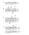
- FIG. 1 is a schematic cross-sectional view of a glass laminate according to the present invention.
- 2A to 2D are schematic cross-sectional views showing an embodiment of a method for producing a glass substrate with a member according to the present invention in the order of steps.
- FIG. 1 is a schematic cross-sectional view of a glass laminate according to the present invention.
- the glass laminate 10 is a laminate in which a support base 12, a glass substrate 16, and a silicone resin layer 14 exist between them.
- the silicone resin layer 14 has one surface in contact with the support base 12 and the other surface in contact with the first main surface 16 a of the glass substrate 16.
- the peel strength at the interface between the silicone resin layer 14 and the first main surface 16 a of the glass substrate 16 is lower than the peel strength at the interface between the silicone resin layer 14 and the support substrate 12, and the silicone resin layer 14.
- the glass substrate 16 are separated from each other and separated into a laminate of the silicone resin layer 14 and the support base 12 and the glass substrate 16.
- the silicone resin layer 14 is fixed on the support base 12, and the glass substrate 16 is detachably laminated on the silicone resin layer 14.
- the two-layer portion composed of the support base 12 and the silicone resin layer 14 reinforces the glass substrate 16 in a member forming process for manufacturing a member for an electronic device such as a liquid crystal panel.
- the two-layer part which consists of the support base material 12 manufactured in advance for manufacture of the glass laminated body 10 and the silicone resin layer 14 is called the support base material 18 with a resin layer.
- the glass laminate 10 is used until a member forming step described later. That is, the glass laminate 10 is used until a member for an electronic device such as a liquid crystal display device is formed on the surface of the second main surface 16b of the glass substrate 16. Then, the glass laminated body in which the member for electronic devices was formed is isolate
- the glass laminate is heated under high temperature conditions (eg, 550 ° C.). The cohesive failure of the silicone resin layer 14 can be suppressed.
- the silicone resin layer 14 is subjected to the following evaluation, and the stress difference ( ⁇ f ) between the stress ⁇ f (C) at the curing temperature of the silicone resin layer and the stress ⁇ f (500) at 500 ° C. obtained by the following formula (1). Is 10 to 105 MPa.
- the stress difference ( ⁇ f ) of the silicone resin layer 14 is obtained by obtaining the stress at two specific temperatures and taking the difference.
- a curvature radius R 0 of warpage at 25 ° C. of a silicon wafer (crystal orientation 100 plane) is obtained.
- a silicone resin layer was formed on the silicon wafer and heated from 25 ° C. to 500 ° C. at 10 ° C./min, and the curing temperature of the silicone resin layer and the curvature radius R 1 of each warp at 500 ° C. were determined.
- the stress ⁇ f (C) of the silicone resin layer at the curing temperature of the silicone resin layer and the stress ⁇ f (500) of the silicone resin layer at 500 ° C. are calculated based on the Stoney equation, and the difference ⁇ f1 between them is calculated. Get.
- ⁇ f1
- (1) ⁇ f (T) ⁇ E s t s 2 / 6t f (1- ⁇ s) ⁇ ⁇ (1 / R 1 -1 / R 0): stress of the silicone resin layer at a temperature T ° C.
- T Stress was measured Temperature (°C)
- C Curing temperature of the silicone resin layer (° C.)
- t f thickness of the silicone resin layer ( ⁇ m)
- t s silicon wafer thickness (mm)
- R 0 radius of curvature (m) of silicon wafer (crystal orientation 100 plane) at 25 ° C.
- R 1 radius of curvature of silicon wafer and silicone resin layer (m)
- E S Elastic modulus of silicon wafer (Pa)
- ⁇ s Poisson's ratio of silicon wafer
- the stress difference ( ⁇ f1 ) when heated from the curing temperature of the silicone resin layer to 500 ° C. when the thickness t f of the silicone resin layer 14 is 1 ⁇ m is preferably 10 to 105 MPa. .
- the stress difference ( ⁇ f2 ) when heated from 40 ° C. when the thickness t f of the silicone resin layer 14 is 1 ⁇ m to the curing temperature of the silicone resin layer 14 is 10 to 50 MPa. preferable.
- the stress difference ( ⁇ f1 ) when heated from the curing temperature of the silicone resin layer to 500 ° C. when the thickness t f of the silicone resin layer 14 is 1 ⁇ m is 10 to 105 MPa
- the difference in stress ( ⁇ f2 ) when heated from 1 to the curing temperature of the silicone resin layer is as small as 10 to 50 MPa
- the glass substrate 16 is heated when the glass laminate is heated under high temperature conditions (eg, 550 ° C.). Peeling from the silicone resin layer 14 can be suppressed.
- the silicone resin constituting the silicone resin layer 14 preferably includes at least an organosiloxy unit (T unit) represented by (R) SiO 3/2 (R represents a hydrogen atom or an organic group). Moreover, it is preferable to contain this unit as a main silicon-containing bond unit.
- T unit organosiloxy unit represented by (R) SiO 3/2
- R represents a hydrogen atom or an organic group
- the silicone resin layer 14 more preferably contains inorganic fine particles in addition to containing at least an organosiloxy unit (T unit) represented by (R) SiO 3/2 .
- the primary particle diameter of the inorganic fine particles is preferably 1 nm to 100 nm, more preferably 5 nm to 50 nm, and still more preferably 10 nm to 25 nm.
- the primary particle diameter of the inorganic fine particles is preferably 10 nm to 25 nm from the viewpoint of dispersibility in the silicone resin layer.
- examples of the inorganic fine particles include silica, alumina, titania, ceria, zirconia, and the like. Of these, silica is preferably used. These are preferably those in which inorganic fine particles are dispersed in water or an organic solvent, and more preferably those in which the inorganic fine particles are dispersed in an organic solvent.
- the ratio of silica contained in the silicone resin layer is preferably 1 to 40 vol%, more preferably 2 to 35 vol%, and most preferably 3 to 30 vol% of the silicone resin layer.
- the ratio of silica contained in the silicone resin layer is 1 to 40 vol%, sufficient heat resistance can be secured in the obtained silicone resin layer, and the glass substrate peels off from the support substrate after high-temperature heating (for example, 550 ° C.). There is no fear. Moreover, it can prevent that a glass substrate peels from a silicone resin layer and does not become a glass laminated body by the ratio of a silica being 40 vol% or less.
- the thickness of the silicone resin layer 14 is not particularly limited, but the upper limit is preferably 100 ⁇ m (that is, 100 ⁇ m or less), more preferably 50 ⁇ m, and even more preferably 10 ⁇ m. Although a lower limit will not be specifically limited if it is the thickness which can peel, It is preferable that it is 0.001 micrometer or more. When the thickness of the silicone resin layer 14 is in such a range, cracks are unlikely to occur in the silicone resin layer 14, and even if bubbles or foreign substances are present between the silicone resin layer 14 and the glass substrate 16, Generation
- the above-mentioned thickness is intended to be an average thickness, and the thickness of the silicone resin layer 14 at an arbitrary position of 5 or more is measured with a contact-type film thickness measuring device, and these are arithmetically averaged.
- the silicone resin layer 14 may be composed of two or more layers.
- “the thickness of the silicone resin layer 14” means the total thickness of all the silicone resin layers.
- the interface between the support substrate 12 and the silicone resin layer 14 has a peel strength (x), and a stress in the peeling direction exceeding the peel strength (x) is applied to the interface between the support substrate 12 and the silicone resin layer 14. And the interface of the support base material 12 and the silicone resin layer 14 peels.
- the interface between the silicone resin layer 14 and the glass substrate 16 has a peel strength (y), and when a stress in the peeling direction exceeding the peel strength (y) is applied to the interface between the silicone resin layer 14 and the glass substrate 16, The interface between the silicone resin layer 14 and the glass substrate 16 is peeled off.
- the peel strength (x) is higher than the peel strength (y). Therefore, when a stress is applied to the glass laminate 10 in the direction in which the support base 12 and the glass substrate 16 are peeled off, the glass laminate 10 is peeled off at the interface between the silicone resin layer 14 and the glass substrate 16 and glass It isolate
- the peel strength (x) is preferably sufficiently higher than the peel strength (y). Increasing the peel strength (x) means that the adhesion of the silicone resin layer 14 to the support base 12 can be increased, and a relatively higher adhesion to the glass substrate 16 can be maintained after the heat treatment. .
- silicone resin layer 14 In order to increase the adhesion of the silicone resin layer 14 to the support substrate 12, it is preferable to form a silicone resin layer by crosslinking and curing curable silicone described later on the support substrate 12.
- the silicone resin layer 14 bonded to the support substrate 12 with a high bonding force can be formed by the adhesive force at the time of crosslinking and curing.
- the bonding force of the silicone resin layer after crosslinking and curing to the glass substrate 16 is usually lower than the bonding force generated during the crosslinking and curing. Therefore, the glass laminate 10 can be manufactured by forming the silicone resin layer 14 on the support base 12 and then laminating the glass substrate 16 on the surface of the silicone resin layer 14.
- the method of using a predetermined silicone resin layer is mentioned,
- the method is not limited.
- each layer (support base material 12, glass substrate 16, silicone resin layer 14) constituting the glass laminate 10 will be described in detail, and then a method for manufacturing the glass laminate will be described in detail.
- the support base 12 supports the glass substrate 16 and prevents deformation, scratches, breakage, etc. of the glass substrate 16 during the manufacture of the electronic device member in a member forming step (step of manufacturing the electronic device member) described later. To prevent.
- the support substrate 12 for example, a metal plate such as a glass plate, a plastic plate, or a SUS plate is used.
- the support base 12 is preferably formed of a material having a small difference in linear expansion coefficient from the glass substrate 16 and more preferably formed of the same material as the glass substrate 16.
- the support base 12 is a glass plate.
- the support base 12 is preferably a glass plate made of the same glass material as the glass substrate 16.
- the support base 12 may be a laminate including two or more layers.
- glass when glass is adopted as the material of the support substrate 12, for example, glass having various compositions such as glass containing alkali metal oxide (soda lime glass) and non-alkali glass can be used. Of these, alkali-free glass is preferred because of its low thermal shrinkage.
- the thickness of the support base 12 may be thicker or thinner than the glass substrate 16.
- the thickness of the support base 12 is selected based on the thickness of the glass substrate 16, the thickness of the silicone resin layer 14, and the thickness of the glass laminate 10.
- the thickness of the support base 12 is set to 0.4 mm. In general, the thickness of the support base 12 is preferably 0.2 to 5.0 mm.
- the thickness of the glass plate is preferably 0.08 mm or more for reasons such as being easy to handle and difficult to break. Further, the thickness of the glass plate is preferably 1.0 mm or less because the rigidity is desired so that the glass plate is appropriately bent without being broken when it is peeled off after forming the electronic device member.
- the difference in linear expansion coefficient between the support base 12 and the glass substrate 16 is preferably 150 ⁇ 10 ⁇ 7 / ° C. or less, more preferably 100 ⁇ 10 ⁇ 7 / ° C. or less, and further preferably 50 ⁇ 10 10. -7 / ° C or less. If the difference is too large, the glass laminate 10 may be severely warped or the support substrate 12 and the glass substrate 16 may be peeled off during heating and cooling in the member forming process. When the material of the support base material 12 is the same as the material of the glass substrate 16, it can suppress that such a problem arises.
- the 1st main surface 16a touches the silicone resin layer 14, and the member for electronic devices is provided in the 2nd main surface 16b on the opposite side to the silicone resin layer 14 side.
- the type of the glass substrate 16 may be a general one, and examples thereof include a glass substrate for a display device such as an LCD or an OLED.
- the glass substrate 16 is excellent in chemical resistance and moisture permeability and has a low heat shrinkage rate.
- As an index of the heat shrinkage rate a linear expansion coefficient defined in JIS R 3102 (revised in 1995) is used.
- the glass substrate 16 is obtained by melting a glass raw material and molding the molten glass into a plate shape.
- a molding method may be a general one, and examples thereof include a float method, a fusion method, a slot down draw method, a full coal method, and a rubber method.
- the glass substrate 16 having a particularly small thickness can be obtained by heating a glass once formed into a plate shape to a moldable temperature and then stretching it by means of stretching or the like to make it thin (redraw method).
- the type of glass of the glass substrate 16 is not particularly limited, but non-alkali borosilicate glass, borosilicate glass, soda lime glass, high silica glass, and other oxide-based glasses mainly composed of silicon oxide are preferable.
- oxide-based glass a glass having a silicon oxide content of 40 to 90% by mass in terms of oxide is preferable.
- a glass substrate for a liquid crystal panel is a glass that does not substantially contain an alkali metal component (non-alkali glass) because the elution of the alkali metal component easily affects the liquid crystal. Included).
- the glass of the glass substrate 16 is appropriately selected based on the type of device to be applied and its manufacturing process.
- the thickness of the glass substrate 16 is preferably 0.3 mm or less, more preferably 0.15 mm or less, from the viewpoint of reducing the thickness and / or weight of the glass substrate 16. In the case of 0.3 mm or less, it is possible to give good flexibility to the glass substrate 16. In the case of 0.15 mm or less, the glass substrate 16 can be rolled up.
- the thickness of the glass substrate 16 is preferably 0.03 mm or more for reasons such as easy manufacture of the glass substrate 16 and easy handling of the glass substrate 16.
- the glass substrate 16 may be composed of two or more layers.
- the material forming each layer may be the same material or a different material.
- the thickness of the glass substrate 16 means the total thickness of all the layers.
- the silicone resin layer 14 prevents the glass substrate 16 from being displaced until the operation for separating the glass substrate 16 and the support base 12 is performed, and prevents the glass substrate 16 and the like from being damaged by the separation operation.
- a surface 14 a of the silicone resin layer 14 that contacts the glass substrate 16 is in close contact with the first main surface 16 a of the glass substrate 16.
- the silicone resin layer 14 is bonded to the first main surface 16a of the glass substrate 16 with a weak bonding force, and the peeling strength (y) at the interface is the peeling at the interface between the silicone resin layer 14 and the support base 12. Lower than strength (x).
- the silicone resin layer 14 and the glass substrate 16 are bonded with a bonding force caused by weak adhesive force or van der Waals force. Further, the silicone resin layer 14 is bonded to the surface of the support base 12 with a strong bonding force such as an adhesive force or an adhesive force, and a known method can be adopted as a method for improving the adhesion between the two.
- the silicone resin layer 14 is made of a silicone resin containing a predetermined organosiloxy unit.
- the silicone resin layer 14 is formed on the surface of the support substrate 12 (more specifically, silicone (organopolysiloxane) capable of forming a predetermined silicone resin is crosslinked on the support substrate 12).
- silicone resin in the silicone resin layer 14 can be adhered to the surface of the support base 12 and high bonding strength can be obtained.
- the process for example, process using a coupling agent which produces strong bond strength between the support base material 12 surface and the silicone resin layer 14 is given, and between the support base material 12 surface and the silicone resin layer 14 The binding power of can be increased.
- the silicone resin layer 14 is made of a silicone resin containing a predetermined organosiloxy unit such that the glass laminate exhibits predetermined properties as described above.
- the silicone resin is usually obtained by crosslinking and curing silicone that can be converted into the silicone resin by a curing treatment.
- the silicone in the present invention is a mixture of monomer hydrolyzable organosilane compounds (monomer mixture), or a partially hydrolyzed condensate (organopolysiloxane) obtained by subjecting the monomer mixture to a partial hydrolytic condensation reaction. ) Is preferable. Moreover, the mixture of a partial hydrolysis-condensation product and a monomer may be sufficient.
- the silicone in the present invention is preferably a partially hydrolyzed condensate of a monomer mixture.
- thermosetting a crosslinking reaction by heating
- silicone resin is obtained by thermosetting silicone.
- heating is not necessarily required for curing, and room temperature curing can also be performed.
- the organosiloxy unit includes a monofunctional organosiloxy unit called M unit, a bifunctional organosiloxy unit called D unit, a trifunctional organosiloxy unit called T unit, and a tetrafunctional organosiloxy unit called Q unit.
- the Q unit is a unit that does not have an organic group bonded to a silicon atom (an organic group having a carbon atom bonded to a silicon atom), but is regarded as an organosiloxy unit (silicon-containing bonded unit) in the present invention.
- the monomers forming the M unit, D unit, T unit, and Q unit are also referred to as M monomer, D monomer, T monomer, and Q monomer, respectively.
- organosiloxy units intend the sum total of M unit, D unit, T unit, and Q unit.
- the ratio of the number of M units, D units, T units, and Q units can be calculated from the value of the peak area ratio by 29 Si-NMR.
- the siloxane bond is a bond in which two silicon atoms are bonded via one oxygen atom, so that the number of oxygen atoms per silicon atom in the siloxane bond is considered to be 1/2. Expressed as medium O 1/2 . More specifically, for example, in one D unit, one silicon atom is bonded to two oxygen atoms, and each oxygen atom is bonded to a silicon atom of another unit.
- the formula is —O 1/2 — (R) 2 Si—O 1/2 — (R represents a hydrogen atom or an organic group). Since there are two O 1/2 s , the D unit is usually expressed as (R) 2 SiO 2/2 [in other words, (R) 2 SiO].
- an oxygen atom O * bonded to another silicon atom is an oxygen atom bonded between two silicon atoms, and is intended to be an oxygen atom in a bond represented by Si—O—Si. To do. Accordingly, one O * exists between the silicon atoms of two organosiloxy units.
- the M unit means an organosiloxy unit represented by (R) 3 SiO 1/2 .
- R represents a hydrogen atom or an organic group.
- the number (here 3) described after (R) means that three hydrogen atoms or organic groups are connected. That is, the M unit has one silicon atom, three hydrogen atoms or an organic group, and one oxygen atom O * . More specifically, the M unit has three hydrogen atoms or organic groups bonded to one silicon atom and an oxygen atom O * bonded to one silicon atom.
- the D unit means an organosiloxy unit represented by (R) 2 SiO 2/2 (R represents a hydrogen atom or an organic group). That is, the D unit is a unit having one silicon atom, two hydrogen atoms or organic groups bonded to the silicon atom, and two oxygen atoms O * bonded to other silicon atoms.
- the T unit means an organosiloxy unit represented by (R) SiO 3/2 (R represents a hydrogen atom or an organic group). That is, the T unit is a unit having one silicon atom, one hydrogen atom or organic group bonded to the silicon atom, and three oxygen atoms O * bonded to another silicon atom.
- Q unit means an organosiloxy unit represented by SiO 2 . That is, the Q unit is a unit having one silicon atom and four oxygen atoms O * bonded to other silicon atoms.
- Examples of the organic group include alkyl groups such as a methyl group, an ethyl group, a propyl group, a butyl group, a pentyl group, a hexyl group, a cyclohexyl group, and a heptyl group; a phenyl group, a tolyl group, a xylyl group, and a naphthyl group.
- the organic group is preferably an unsubstituted or halogen-substituted monovalent hydrocarbon group having preferably 1 to 12 carbon atoms (more preferably about 1 to 10 carbon atoms).
- the silicone resin can be manufactured using a known material.
- the silicone that can be converted into the silicone resin by curing treatment includes a mixture of monomer hydrolyzable organosilane compounds (monomer mixture) and / or partial hydrolysis condensation obtained by partial hydrolysis condensation reaction of the monomer mixture.
- the product organopolysiloxane is used.
- the type of monomer used is not particularly limited as long as the above-described silicone resin having a predetermined organosiloxy unit is obtained.
- the manufacturing method of the silicone resin layer 14 described above is not particularly limited, and a known method can be adopted.
- the composition may contain a solvent, and in this case, the thickness of the silicone resin layer 14 can be controlled by adjusting the concentration of the solvent.
- the silicone content in the composition is 1 to 100% by mass with respect to the total mass of the composition because it is easy to handle and the film thickness of the silicone resin layer 14 is more easily controlled. 1 to 50% by mass is more preferable.
- the solvent is not particularly limited as long as the composition can be easily dissolved in a working environment and can be easily volatilized and removed.
- the boiling point of the solvent is not particularly limited, but is preferably 270 ° C. or lower, more preferably 250 ° C. or lower, and 230 ° C. or lower because it is easy to remove and can prevent deterioration of the resin layer when the solvent is removed by heating.
- the following is more preferable.
- a minimum in particular is not restrict
- the Hildebrand parameter (hereinafter referred to as SP value) of the solvent is not particularly limited, but is preferably 10 to 25 and more preferably 15 to 20 from the viewpoint that it can be easily dissolved in the composition.
- the surface tension value of the solvent is not particularly limited, but is 10 to 40 mN / m, which is close to the surface tension value of the composition, from the viewpoint of easily maintaining the smoothness of the film surface when a concentration distribution occurs in the coated film surface during drying. Is preferable, and 15 to 30 mN / m is more preferable.
- the rheology of the coating solution is not particularly limited, but preferably has a thixotropic property because the viscosity is low during coating and the viscosity is high when the solvent is removed, and a smooth coated surface is easily formed.
- a curing catalyst may be included in the composition as necessary.
- the curing catalyst is a catalyst that accelerates the hydrolysis reaction and / or condensation reaction of silicone.
- Examples of the curing catalyst include acidic and basic catalysts and organometallic curing catalysts.
- the curing catalyst is preferably an organometallic curing catalyst, for example, organotin compounds such as diacetyltin diacetate, dibutyltin dilaurate, dibutyltin diacetate and tin octylate; aluminum trimethoxide, aluminum tris (acetylacetonate) Organic aluminum compounds such as aluminum tri-n-butoxide and aluminum tris (acetoacetate ethyl); organic titanium compounds such as titanium tetramethoxide, titanium tetraethoxide, titanium tetrabutoxide and titanium tetraisopropoxide; zirconium tetra (monomethyl) Ethoxide), zirconium tetra (monoethyl ethoxide) and zirconium tetra (monobutyl ethoxide) and other organic zirconium compounds. These may be used alone or in combination of two or more.
- organotin compounds such as diace
- the amount of the curing catalyst used is not particularly limited, but is preferably from 0.01 to 20 parts by weight, more preferably from 0.05 to 10 parts by weight based on 100 parts by weight of the silicone contained in the composition from the viewpoint that the effects of the present invention are more excellent. Part by mass is more preferable.
- the composition may contain various additives.
- a leveling agent may be included.
- the leveling agent include fluorine-based leveling agents such as Megafac F558, Megafac F560, and Megafac F561 (all manufactured by DIC).
- a leveling agent in which the surface tension (mN / m) of the 0.1% PGME solution is preferably 19 (mN / m) to 27 (mN / m) is preferable. 20 (mN / m) to 25 (mN / m) is more preferable, and 22 (mN / m) to 24 (mN / m) is more preferable.
- the glass laminate 10 of the present invention is a laminate in which the support base 12, the glass substrate 16, and the silicone resin layer 14 exist between them.
- the manufacturing method of the glass laminated body 10 of this invention is not restrict
- the silicone resin layer 14 is formed on the support base material 12 surface.
- a composition containing silicone is applied to the surface of the support substrate 12 and subjected to a curing treatment to form the silicone resin layer 14 on the surface of the support substrate 12, and then the silicone resin surface of the silicone resin layer 14.
- a method of manufacturing the glass laminate 10 by laminating the glass substrate 16 is preferable.
- the composition containing silicone When the composition containing silicone is cured on the surface of the support substrate 12, it adheres due to the interaction with the surface of the support substrate 12 during the curing reaction, and the peel strength between the silicone resin layer 14 and the surface of the support substrate 12 increases. Conceivable. Therefore, even if the glass substrate 16 and the support base 12 are made of the same material, a difference can be provided in the peel strength between the silicone resin layer 14 and the both.
- the step of forming the silicone resin layer 14 on the surface of the support substrate 12 is a resin layer forming step
- the step of laminating the glass substrate 16 on the silicone resin surface of the silicone resin layer 14 to form the glass laminate 10 is a lamination step. Good, the procedure of each step will be described in detail.
- the silicone resin layer 14 is formed on the surface of the support base 12. First, it is preferable that a composition in which silicone is dissolved in a solvent is applied on the support substrate 12 and then subjected to a curing treatment to form the silicone resin layer 14.
- the method for applying the composition on the surface of the support substrate 12 is not particularly limited, and a known method can be used. Examples thereof include spray coating, die coating, spin coating, dip coating, roll coating, bar coating, screen printing, and gravure coating.
- a silicone resin layer 14 is formed on the surface of at least one side of the support base 12.
- the curing method is not particularly limited, but is usually performed by a heat curing process.
- the temperature condition for thermosetting is preferably 150 to 550 ° C, more preferably 200 to 450 ° C.
- the heating time is usually preferably 10 to 300 minutes, more preferably 20 to 120 minutes. Note that the heating condition may be implemented stepwise by changing the temperature condition.
- the silicone resin layer 14 excellent in heat resistance can be obtained.
- Precuring is preferably performed following the removal of the solvent. In that case, there is no particular distinction between the step of removing the solvent from the layer to form a crosslinked layer and the step of performing precuring.
- the removal of the solvent is preferably performed by heating to 100 ° C. or higher, and more preferably by preheating to 150 ° C. or higher.
- the temperature at which the solvent is removed and precured and the heating time are preferably 100 to 420 ° C. and 5 to 60 minutes, more preferably 150 to 300 ° C. and 10 to 30 minutes. A silicone resin layer that is easily peeled when the temperature is 420 ° C. or lower is obtained.
- the glass substrate 16 is laminated on the silicone resin surface of the silicone resin layer 14 obtained in the resin layer forming step, and the layer of the supporting base 12, the silicone resin layer 14, and the glass substrate 16 are laminated.
- This is a step of obtaining the glass laminate 10 provided in this order. More specifically, as shown in FIG. 2 (B), a glass substrate having a surface 14a opposite to the support base 12 side of the silicone resin layer 14, and a first main surface 16a and a second main surface 16b.
- the silicone resin layer 14 and the glass substrate 16 are laminated by using the first principal surface 16a of 16 as a lamination surface, and the glass laminate 10 is obtained.
- the method for laminating the glass substrate 16 on the silicone resin layer 14 is not particularly limited, and a known method can be adopted. For example, a method of stacking the glass substrate 16 on the surface of the silicone resin layer 14 under a normal pressure environment can be mentioned.
- the glass substrate 16 may be laminated on the surface of the silicone resin layer 14, and then the glass substrate 16 may be pressure-bonded to the silicone resin layer 14 using a roll or a press. Air bubbles mixed between the silicone resin layer 14 and the glass substrate 16 can be removed relatively easily by pressure bonding using a roll or a press, which is preferable.
- the surface of the glass substrate 16 in contact with the silicone resin layer 14 is sufficiently washed and laminated in a clean environment.
- the conditions for the pre-annealing treatment are appropriately selected according to the type of the silicone resin layer 14 to be used, but the peel strength (y) between the glass substrate 16 and the silicone resin layer 14 is more appropriate. From this point, it is preferable to perform heat treatment at 300 ° C. or higher (more preferably 300 to 400 ° C.), preferably 5 minutes or longer (more preferably 5 to 30 minutes).
- the curable silicone is cured on some peelable surface to produce a silicone resin film.
- the film can be interposed between the glass substrate 16 and the support base 12 and laminated simultaneously.
- the adhesiveness by hardening of curable silicone is low enough with respect to the glass substrate 16, and the adhesiveness is high enough with respect to the support base material 12, a crosslinked material is formed between the glass substrate 16 and the support base material 12.
- the silicone resin layer 14 can be formed by curing.
- the support base 12 is made of the same glass material as that of the glass substrate 16, it is possible to increase the peel strength with respect to the silicone resin layer 14 by performing a treatment for improving the adhesion of the support base 12 surface.
- a chemical method that improves the fixing force chemically such as a silane coupling agent, a physical method that increases surface active groups such as a flame (flame) treatment, or a surface such as a sandblast treatment
- a mechanical treatment method for increasing the catch by increasing the roughness of the material for example, a chemical method (primer treatment) that improves the fixing force chemically such as a silane coupling agent, a physical method that increases surface active groups such as a flame (flame) treatment, or a surface such as a sandblast treatment
- a mechanical treatment method for increasing the catch by increasing the roughness of the material.
- the glass laminate 10 of the present invention can be used for various applications.
- an electronic device such as a display panel, a photovoltaic power generation panel, a thin film secondary battery, and a semiconductor wafer having a circuit formed on the surface, which will be described later.
- the use which manufactures components is mentioned.
- the glass laminate 10 is often exposed (for example, 1 hour or longer) under high temperature conditions (for example, 550 ° C. or higher).
- examples of the display device panel include an LCD, an OLED, an electronic paper, a plasma display panel, a field emission panel, a quantum dot LED panel, and a MEMS (Micro Electro Mechanical Systems) shutter panel.
- an electronic device can be manufactured using the glass laminated body mentioned above.
- the glass laminated body 10 mentioned above the glass substrate with a member (glass substrate with a member for electronic devices) containing a glass substrate and the member for electronic devices is manufactured.
- the manufacturing method of this glass substrate with a member is not specifically limited, From the point which is excellent in productivity of an electronic device, the member for electronic devices is formed on the glass substrate in the said glass laminated body, and the laminated body with an electronic device member is used.
- a method of separating the manufactured and obtained laminated body with a member for electronic devices into a glass substrate with a member and a supporting substrate with a resin layer by using the glass substrate side interface of the silicone resin layer or the inside of the silicone resin layer as a release surface is preferable.
- the step of forming a member for an electronic device by forming a member for an electronic device on the glass substrate in the glass laminate is a member forming step, and the glass substrate for the silicone resin layer from the laminate with the member for an electronic device.
- the step of separating the glass substrate with a member and the support base with a resin layer using the side interface as a separation surface is referred to as a separation step, and the step of cleaning the separation surface of the glass substrate with a member is referred to as a cleaning treatment step.
- the cleaning process process is an arbitrary process implemented as needed.
- a member formation process is a process of forming the member for electronic devices on the glass substrate 16 in the glass laminated body 10 obtained in the said lamination process. More specifically, as shown in FIG. 2C, the electronic device member 22 is formed on the second main surface 16b (exposed surface) of the glass substrate 16 to obtain a laminate 24 with the electronic device member. .
- the electronic device member 22 is a member that is formed on the glass substrate 16 in the glass laminate 10 and constitutes at least a part of the electronic device. More specifically, as the electronic device member 22, a member used for an electronic component such as a display device panel, a solar cell, a thin film secondary battery, or a semiconductor wafer having a circuit formed on the surface (for example, Display member, solar cell member, thin film secondary battery member, electronic component circuit).
- a transparent electrode such as tin oxide of a positive electrode, a silicon layer represented by p layer / i layer / n layer, a metal of a negative electrode, and the like can be given.
- Examples include various members corresponding to a mold, a dye-sensitized type, a quantum dot type, and the like.
- a transparent electrode such as a metal or metal oxide of a positive electrode and a negative electrode, a lithium compound of an electrolyte layer, a metal of a current collecting layer, and a resin as a sealing layer Etc.
- various members corresponding to a nickel hydrogen type, a polymer type, a ceramic electrolyte type, and the like can be given.
- a metal of a conductive part, silicon oxide or silicon nitride of an insulating part, etc. can be mentioned.
- various sensors such as a pressure sensor and an acceleration sensor, a rigid printed board, a flexible printed board, and various members corresponding to a rigid flexible printed board can be used.
- the manufacturing method of the laminated body 24 with the member for electronic devices mentioned above is not specifically limited, According to the conventionally well-known method according to the kind of structural member of the member for electronic devices, the 2nd main of the glass substrate 16 of the glass laminated body 10 is used. The electronic device member 22 is formed on the surface 16b surface.
- the electronic device member 22 is not all of the members finally formed on the second main surface 16b of the glass substrate 16 (hereinafter referred to as “all members”), but a part of all the members (hereinafter referred to as “parts”). May be referred to as a member.
- the glass substrate with a partial member peeled from the silicone resin layer 14 can be used as a glass substrate with an all member (corresponding to an electronic device described later) in the subsequent steps.
- the other electronic device member may be formed on the peeling surface (first main surface 16a) of the glass substrate with all members peeled from the silicone resin layer 14.
- an electronic device can also be manufactured by assembling a laminate with all members and then peeling the support substrate 12 from the laminate with all members. Furthermore, it is also possible to assemble using two laminates with all members, and then peel off the two support bases 12 from the laminate with all members to produce a glass substrate with a member having two glass substrates. it can.
- an organic EL is formed on the surface of the glass laminate 10 opposite to the silicone resin layer 14 side of the glass substrate 16 (corresponding to the second main surface 16b of the glass substrate 16).
- a transparent electrode is formed, and a hole injection layer, a hole transport layer, a light emitting layer, an electron transport layer, etc. are deposited on the surface on which the transparent electrode is formed, a back electrode is formed, and sealing is performed.
- Various layers are formed and processed, such as sealing with a plate. Specific examples of the layer formation and processing include film formation processing, vapor deposition processing, sealing plate adhesion processing, and the like.
- a resist film is used on the second main surface 16b of the glass substrate 16 of the glass laminate 10 by a general film forming method such as a CVD method or a sputtering method.
- a TFT forming step of forming a thin film transistor (TFT) by patterning the formed metal film, metal oxide film, etc., and patterning a resist solution on the second main surface 16b of the glass substrate 16 of another glass laminate 10 Various processes such as a CF forming step for forming a color filter (CF) to be used for forming, a laminating step for laminating a laminated body with TFT obtained in the TFT forming step and a laminated body with CF obtained in the CF forming step, etc. Process.
- TFTs and CFs are formed on the second main surface 16b of the glass substrate 16 using a well-known photolithography technique, etching technique, or the like. At this time, a resist solution is used as a coating solution for pattern formation.
- a cleaning method known dry cleaning or wet cleaning can be used.
- the thin film transistor forming surface of the laminated body with TFT and the color filter forming surface of the laminated body with CF are opposed to each other, and are bonded using a sealant (for example, an ultraviolet curable sealant for cell formation).
- a sealant for example, an ultraviolet curable sealant for cell formation.
- a liquid crystal material is injected into a cell formed by the laminate with TFT and the laminate with CF.
- the method for injecting the liquid crystal material include a reduced pressure injection method and a dropping injection method.
- the separation step is performed by using the electronic device member-attached laminate 24 obtained in the member formation step as an exfoliation surface at the interface between the silicone resin layer 14 and the glass substrate 16.
- the glass substrate 16 with a member including the electronic device member 22 and the glass substrate 16 is obtained by separating the glass substrate 16 (glass substrate with a member) on which the member 22 for use is laminated, the silicone resin layer 14, and the support base 12. It is a process.
- the remaining constituent members can be formed on the glass substrate 16 after separation.
- the method of peeling the glass substrate 26 with a member and the support base material 18 with a resin layer is not specifically limited. Specifically, for example, a sharp blade-like object is inserted into the interface between the glass substrate 16 and the silicone resin layer 14 to give a trigger for peeling, and then a mixed fluid of water and compressed air is sprayed. Can be peeled off.
- the electronic device member-attached laminate 24 is placed on the surface plate so that the support base material 12 is on the upper side and the electronic device member 22 side is on the lower side, and the electronic device member 22 side is vacuumed on the surface plate.
- Adsorbs (sequentially performed when supporting substrates are laminated on both sides).
- a blade is made to enter the interface between the glass substrate 16 and the silicone resin layer 14.
- the support substrate 12 side is sucked by a plurality of vacuum suction pads, and the vacuum suction pads are raised in order from the vicinity of the place where the blade is inserted.
- an air layer is formed at the interface between the silicone resin layer 14 and the glass substrate 16, and the air layer spreads over the entire interface, so that the support substrate 18 with a resin layer can be easily peeled off.
- the support base material 18 with a resin layer can be laminated
- the fragments of the silicone resin layer 14 are electrostatically adsorbed to the glass substrate 26 with a member by controlling the spraying and humidity with an ionizer. It can be suppressed more.
- the cleaning treatment step is a step of performing a cleaning treatment on the peeling surface (first main surface 16a) of the glass substrate 16 in the glass substrate with member 26 obtained in the separation step.
- This step it is possible to remove impurities such as silicone resin and silicone resin layer adhering to the release surface, metal pieces and dust generated in the member forming step adhering to the release surface, and cleaning the release surface. Sex can be maintained. As a result, the tackiness of a retardation film, a polarizing film or the like attached to the release surface of the glass substrate 16 is improved.
- the cleaning treatment method is not particularly limited as long as the resin or dust attached to the release surface can be removed.
- a method of thermally decomposing the deposit there are a method of thermally decomposing the deposit, a method of removing impurities on the peeled surface by plasma irradiation or light irradiation (for example, UV irradiation treatment), and a cleaning method using a solvent.
- the above-described method for manufacturing the glass substrate with member 26 is suitable for manufacturing a small display device used for a mobile terminal such as a mobile phone or a PDA.
- the display device is mainly an LCD or OLED.
- Examples of the LCD include TN type, STN type, FE type, TFT type, MIM type, IPS type, and VA type.
- the present invention can be applied to both passive drive type and active drive type display devices.
- the glass substrate 26 with a member manufactured by the above method for example, a panel for a display device having a glass substrate and a member for a display device, a solar cell having a glass substrate and a member for a solar cell, a glass substrate and a thin film secondary battery.
- a thin-film secondary battery having a member and an electronic component having a glass substrate and a member for an electronic device.
- the display device panel include a liquid crystal panel, an organic EL panel, a plasma display panel, and a field emission panel.
- an electronic device can also be manufactured using the glass laminated body 100 according to the procedure similar to the above.
- the support base material 12, the silicone resin layer 14, and the glass substrate 16 are set by making the interface of the support base material 12 and the silicone resin layer 14 into a peeling surface.
- an electronic device including the electronic device member 22.
- Examples 1-1, 1-2, 1-3 and 2 to 5 are examples, and Examples 6 to 10 are comparative examples.
- Example 1-1, 1-2, 1-3> A colloidal silica dispersion obtained by dispersing diisobutyl ketone (Kanto Chemical Co., Inc.) and silica particles having a particle diameter of 10 nm in ethylene glycol monopropyl ether at a concentration of 30% by mass into Resin 1 is adjusted so that the silica particle addition rate is 13 vol%. The amount was adjusted and mixed to obtain a solution having a solid content of 30% by mass. The amine-based dispersion aid was added at 3.4% by mass with respect to the silica particle solid content, and acetic acid was added as a solution stabilizer at 50 mol% with respect to the dispersion aid. A coating solution 1 was obtained by filtration through a 0.2 ⁇ m syringe filter.
- Example 2 A colloidal silica dispersion obtained by dispersing diisobutyl ketone (Kanto Chemical Co., Inc.) and silica particles having a particle size of 10 nm in ethylene glycol monopropyl ether at a concentration of 30% by mass into resin 1 is adjusted so that the silica particle addition rate is 19 vol%. The amount was adjusted and mixed to obtain a solution having a solid content of 30% by mass. The amine-based dispersion aid was added at 3.4% by mass with respect to the silica particle solid content, and acetic acid was added as a solution stabilizer at 50 mol% with respect to the dispersion aid. A coating solution 2 was obtained by filtration through a 0.2 ⁇ m syringe filter.
- Example 3 A colloidal silica dispersion obtained by dispersing diisobutyl ketone (Kanto Chemical), silica particles having a particle size of 10 nm in ethylene glycol monopropyl ether at a concentration of 30% by mass into resin 1 so that the silica particle addition rate is 26 vol%. The amount was adjusted and mixed to obtain a solution having a solid content of 30% by mass. The amine-based dispersion aid was added at 3.4% by mass with respect to the silica particle solid content, and acetic acid was added as a solution stabilizer at 50 mol% with respect to the dispersion aid. The solution was filtered with a 0.2 ⁇ m syringe filter to obtain a coating solution 3.
- diisobutyl ketone Korean Chemical
- the amount was adjusted and mixed
- Example 4 Cyclohexanone (Kanto Chemical) and silica fine particles with a particle diameter of 10 nm were mixed in a 50 mass% toluene solution of resin 2 while adjusting the amount of cyclohexanone so that the silica particle addition rate was 5 vol%, and the solid content was 30 mass%. A solution was obtained. Ti (OBu) 4 was added to the solution in an amount of 0.5 mass% of the solid content of the resin 2, and the solution was filtered through a 0.2 ⁇ m syringe filter to obtain a coating solution 4.
- Example 5 Cyclohexanone (Kanto Chemical) and silica fine particles with a particle diameter of 10 nm were mixed in a 50 mass% toluene solution of resin 2 while adjusting the amount of cyclohexanone so that the silica particle addition rate was 15 vol%, and the solid content was 30 mass%. A solution was obtained. Ti (OBu) 4 was added to the solution in an amount of 0.5 mass% of the solid content of the resin 2, and the solution was filtered through a 0.2 ⁇ m syringe filter to obtain a coating solution 5.
- Example 6 The amount of diisobutyl ketone was adjusted and mixed with the resin 1 to obtain a solution having a solid content of 30% by mass. A coating solution 6 was obtained by filtration through a 0.2 ⁇ m syringe filter.
- Example 7 A 1-liter flask was charged with 200 g of water-dispersed colloidal silica (pH 3.1, solid content 35 mass%) having an average particle diameter of about 15 nm and 0.2 g of acetic acid, and 138 g of methyltrimethoxysilane was added. After stirring for 1 hour, the pH of the composition stabilized at 4.5. This composition was aged at 25 ° C. for 4 days to ensure partial hydrolysis condensation in a silica-methanol-water dispersion.
- This composition has a non-volatile component of 40% by mass (150 ° C., 45 minutes), and the obtained organopolysiloxane has a bond structure mainly composed of T units (number of T units: M units, D units, and Q units, respectively).
- organopolysiloxane composition solution PSi-1 (PSi-1 concentration: 16) with a non-volatile component of 25% by mass (150 ° C., 45 minutes) and a viscosity of 4.4 mPa ⁇ s .8 mass%) was prepared and filtered with a 0.2 ⁇ m syringe filter to obtain a coating solution 7.
- Example 8> A 50 mass% toluene solution of the resin 3 was filtered with a 0.2 ⁇ m syringe filter to obtain a coating solution 8.
- a colloidal silica dispersion obtained by dispersing silica particles having a particle diameter of 10 nm in ethylene glycol monopropyl ether at a concentration of 30% by mass in a 50% by mass toluene solution of Resin 3 has a diisobutyl ketone amount of 19 vol%.
- the amine-based dispersion aid was added at 3.4% by mass with respect to the silica particle solid content, and acetic acid was added as a solution stabilizer at 50 mol% with respect to the dispersion aid.
- a coating solution 9 was obtained by filtration through a 0.2 ⁇ m syringe filter.
- Example 10 A colloidal silica dispersion obtained by dispersing silica particles having a particle diameter of 10 nm in a 50 mass% toluene solution of resin 4 in ethylene glycol monopropyl ether at a concentration of 30 mass% is adjusted so that the addition rate of silica particles is 19 vol%.
- the amine-based dispersion aid was added at 3.4% by mass with respect to the silica particle solid content, and acetic acid was added as a solution stabilizer at 50 mol% with respect to the dispersion aid.
- the solution was filtered with a 0.2 ⁇ m syringe filter to obtain a coating solution 10.
- Silicone resin composition analysis The silicone resin composition was determined by measuring 1 H NMR, 29 Si NMR and 13 C NMR. 1 H NMR, 29 Si NMR and 13 C NMR were measured using AVANCE-3-HD400 manufactured by Bruker Biospin. Heavy acetone was used as a solvent for measurement, and Cr (acac) 3 was prepared and added so as to be 0.1% by mass with respect to the sample as a relaxation reagent. Tetramethylsilane was used as a standard. The sample concentration was adjusted to about 20 wt% and measured.
- Example 1 [Laminated substrate production] The obtained coating solutions 1 to 10 were applied by spin coating to a glass substrate (“AN100” manufactured by Asahi Glass Co., Ltd.) having a size of 100 ⁇ 100 mm and a thickness of 0.5 mm, and heated at 100 ° C. for 10 minutes with a hot plate. Thereafter, Examples 1-1 and 2 to 10 were heated in an oven at 250 ° C. for 30 minutes in the atmosphere to obtain a silicone resin layer (curing temperature 250 ° C.). In Example 1-2, heating was performed in the atmosphere at 300 ° C. for 30 minutes to obtain a silicone resin layer (curing temperature 300 ° C.). In Example 1-3, heating was performed at 350 ° C.
- AN100 manufactured by Asahi Glass Co., Ltd.
- a silicone resin layer (curing temperature 350 ° C.). It cooled to 25 degreeC and obtained the silicone resin layer with a film thickness of 2 micrometers. Thereafter, a glass substrate having a size of 100 ⁇ 100 mm and a thickness of 0.2 mm (“AN100” manufactured by Asahi Glass Co., Ltd.) was placed on the silicone resin layer and bonded with a bonding apparatus to prepare a laminated substrate.
- AN100 manufactured by Asahi Glass Co., Ltd.
- the film thickness was measured with a surface roughness measuring device Surfcom 1400G-12 (manufactured by Tokyo Seimitsu Co., Ltd.), and it was confirmed that the film thickness was 1 ⁇ m.
- a curvature radius R 0 of warpage at 25 ° C. of a silicon wafer (crystal orientation 100 plane) is obtained.
- a silicone resin layer is formed on the silicon wafer and heated from 25 ° C. to 500 ° C. at a rate of 10 ° C./min., Respectively, at 40 ° C., the curing temperature of the silicone resin layer (Example 1-1 and Examples 2 to 10 are ⁇ f (40) , ⁇ f (C) and ⁇ f (500) , which are stresses of the silicone resin layer at 250 ° C., 300 ° C. for Example 1-2 and 350 ° C. for Example 1-3) and 500 ° C., were calculated. .
- ⁇ f1
- (1) ⁇ f2
- (2) ⁇ f (T) ⁇ E s t s 2 / 6t f (1- ⁇ s) ⁇ ⁇ (1 / R 1 -1 / R 0): stress of the silicone resin layer at a temperature T ° C.
- T Stress was measured Temperature (°C)
- C Curing temperature of the silicone resin layer (° C.)
- t f thickness of the silicone resin layer ( ⁇ m)
- t s silicon wafer thickness (mm)
- R 0 radius of curvature (m) of silicon wafer (crystal orientation 100 plane) at 25 ° C.
- R 1 radius of curvature of silicon wafer and silicone resin layer (m)
- E S Elastic modulus of silicon wafer (Pa)
- ⁇ s Poisson's ratio of silicon wafer
- Examples 1-1 to 1-3 and 2 to 5 which are examples have ⁇ f1 in the range of 10 to 105 MPa and ⁇ f2 in the range of 10 to 50 MPa.
- the heat-resistant foaming property and cracking property were both good.
- ⁇ f1 was outside the range of 10 to 105 MPa, and cracks occurred from the silicone resin layer toward the inside.
- ⁇ f1 could not be measured due to the occurrence of cracks
- ⁇ f2 was also outside the range of 10 to 50 MPa, and the heat resistant foaming property and cracking property were low.
Landscapes
- Chemical & Material Sciences (AREA)
- Organic Chemistry (AREA)
- Engineering & Computer Science (AREA)
- Chemical Kinetics & Catalysis (AREA)
- Ceramic Engineering (AREA)
- Life Sciences & Earth Sciences (AREA)
- General Chemical & Material Sciences (AREA)
- Geochemistry & Mineralogy (AREA)
- Materials Engineering (AREA)
- Inorganic Chemistry (AREA)
- Thermal Sciences (AREA)
- Physics & Mathematics (AREA)
- Laminated Bodies (AREA)
- Joining Of Glass To Other Materials (AREA)
Abstract
Description
前記シリコーン樹脂層は、下記評価を行い、下記式(1)より求めたシリコーン樹脂層の硬化温度における応力σf(C)と500℃における応力σf(500)との応力差Δσf1が10~105MPaであることを特徴とするガラス積層体に関する。
評価:シリコンウエハ(結晶方位100面)の25℃での反りの曲率半径R0を求める。次にそのシリコンウエハ上にシリコーン樹脂層を形成し、25℃から500℃まで10℃/分で加熱し、シリコーン樹脂層の硬化温度と、500℃におけるそれぞれの反りの曲率半径R1を求めた上で、Stoneyの式に基づいて、シリコーン樹脂層の硬化温度におけるシリコーン樹脂層の応力σf(C)と500℃におけるシリコーン樹脂層の応力σf(500)を算出し、これらの差Δσf1を得る。
Δσf1=|(シリコーン樹脂層の硬化温度におけるシリコーン樹脂層の応力σf(C))-(500℃におけるシリコーン樹脂層の応力σf(500))|・・・(1)
σf(T)={Ests 2/6tf(1-νs)}×(1/R1-1/R0):温度T℃におけるシリコーン樹脂層の応力
T: 応力を測定した温度(℃)
C: シリコーン樹脂層の硬化温度(℃)
tf:シリコーン樹脂層の厚み(μm)
ts:シリコンウエハの厚み(mm)
R0:25℃におけるシリコンウエハ(結晶方位100面)の曲率半径(m)
R1:シリコンウエハとシリコーン樹脂層の曲率半径(m)
ES:シリコンウエハの弾性率(Pa)
νs:シリコンウエハのポアソン比
Δσf1=|(シリコーン樹脂層の硬化温度におけるシリコーン樹脂層の応力σf(C))-(500℃におけるシリコーン樹脂層の応力σf(500))|・・・(1)
σf(T)={Ests 2/6tf(1-νs)}×(1/R1-1/R0):温度T℃におけるシリコーン樹脂層の応力
T: 応力を測定した温度(℃)
C: シリコーン樹脂層の硬化温度(℃)
tf:シリコーン樹脂層の厚み(μm)
ts:シリコンウエハの厚み(mm)
R0:25℃におけるシリコンウエハ(結晶方位100面)の曲率半径(m)
R1:シリコンウエハとシリコーン樹脂層の曲率半径(m)
ES:シリコンウエハの弾性率(Pa)
νs:シリコンウエハのポアソン比
Δσf2=|(40℃におけるシリコーン樹脂層の応力σf(40))-(シリコーン樹脂層の硬化温度におけるシリコーン樹脂層の応力σf(C))|・・・(2)
支持基材12は、ガラス基板16を支持し、後述する部材形成工程(電子デバイス用部材を製造する工程)において電子デバイス用部材の製造の際にガラス基板16の変形、傷付き、破損などを防止する。
ガラス基板16は、第1主面16aがシリコーン樹脂層14と接し、シリコーン樹脂層14側とは反対側の第2主面16bに電子デバイス用部材が設けられる。
シリコーン樹脂層14は、ガラス基板16と支持基材12とを分離する操作が行われるまでガラス基板16の位置ずれを防止すると共に、ガラス基板16などが分離操作によって破損するのを防止する。シリコーン樹脂層14のガラス基板16と接する表面14aは、ガラス基板16の第1主面16aに密着する。シリコーン樹脂層14はガラス基板16の第1主面16aに弱い結合力で結合しており、その界面の剥離強度(y)は、シリコーン樹脂層14と支持基材12との間の界面の剥離強度(x)よりも低い。
本発明のガラス積層体10は、上述したように、支持基材12とガラス基板16とそれらの間にシリコーン樹脂層14が存在する積層体である。
樹脂層形成工程では、支持基材12表面上にシリコーン樹脂層14を形成する。最初に、シリコーンを溶媒に溶解させた組成物を支持基材12上に塗布し、次いで硬化処理を施してシリコーン樹脂層14とすることが好ましい。
積層工程は、上記の樹脂層形成工程で得られたシリコーン樹脂層14のシリコーン樹脂面上にガラス基板16を積層し、支持基材12の層とシリコーン樹脂層14とガラス基板16の層とをこの順で備えるガラス積層体10を得る工程である。より具体的には、図2(B)に示すように、シリコーン樹脂層14の支持基材12側とは反対側の表面14aと、第1主面16aおよび第2主面16bを有するガラス基板16の第1主面16aとを積層面として、シリコーン樹脂層14とガラス基板16とを積層し、ガラス積層体10を得る。
本発明のガラス積層体10は、種々の用途に使用することができ、例えば、後述する表示装置用パネル、太陽光発電パネル、薄膜2次電池、表面に回路が形成された半導体ウエハ等の電子部品を製造する用途などが挙げられる。なお、該用途では、ガラス積層体10が高温条件(例えば、550℃以上)で曝される(例えば、1時間以上)場合が多い。
本発明においては、上述したガラス積層体を用いて、電子デバイスを製造することができる。以下では、上述したガラス積層体10を用いた態様について詳述する。ガラス積層体10を用いることにより、ガラス基板と電子デバイス用部材とを含む部材付きガラス基板(電子デバイス用部材付きガラス基板)が製造される。
部材形成工程は、上記積層工程において得られたガラス積層体10中のガラス基板16上に電子デバイス用部材を形成する工程である。より具体的には、図2(C)に示すように、ガラス基板16の第2主面16b(露出表面)上に電子デバイス用部材22を形成し、電子デバイス用部材付き積層体24を得る。
電子デバイス用部材22は、ガラス積層体10中のガラス基板16上に形成され電子デバイスの少なくとも一部を構成する部材である。より具体的には、電子デバイス用部材22としては、表示装置用パネル、太陽電池、薄膜2次電池、または、表面に回路が形成された半導体ウエハ等の電子部品などに用いられる部材(例えば、表示装置用部材、太陽電池用部材、薄膜2次電池用部材、電子部品用回路)が挙げられる。
上述した電子デバイス用部材付き積層体24の製造方法は特に限定されず、電子デバイス用部材の構成部材の種類に応じて従来公知の方法にて、ガラス積層体10のガラス基板16の第2主面16b表面上に、電子デバイス用部材22を形成する。
分離工程は、図2(D)に示すように、上記部材形成工程で得られた電子デバイス用部材付き積層体24から、シリコーン樹脂層14とガラス基板16との界面を剥離面として、電子デバイス用部材22が積層したガラス基板16(部材付きガラス基板)と、シリコーン樹脂層14および支持基材12とに分離して、電子デバイス用部材22およびガラス基板16を含む部材付きガラス基板26を得る工程である。
清浄化処理工程は、上記分離工程で得られた部材付きガラス基板26中のガラス基板16の剥離面(第1主面16a)に清浄化処理を施す工程である。該工程を実施することにより、剥離面に付着したシリコーン樹脂やシリコーン樹脂層、剥離面に付着した上記部材形成工程で発生する金属片やホコリなどの不純物を除去することができ、剥離面の清浄性を維持することができる。結果として、ガラス基板16の剥離面に貼り付けられる位相差フィルムや偏光フィルムなどの粘着性が向上する。
1リットルのフラスコに、トリエトキシメチルシラン179g、トルエン300g、酢酸を5g加えて25℃で20分間撹拌後60℃に加熱して12時間反応した。25℃に冷却後、水を300g加えて反応粗液を3回洗浄した。反応粗液からトルエンを減圧留去しスラリー状態にした後、真空乾燥機で終夜乾燥することで白色のオルガノポリシロキサン固体である樹脂1が得られた。
1リットルのフラスコに、トリエトキシメチルシラン150g、ジエトキシジメチルシラン21g、トルエン250g、酢酸を7g加えて25℃で20分間撹拌後、100℃に加熱して12時間反応した。25℃に冷却後、水を300g加えて反応粗液を3回洗浄した。反応粗液からトルエンを減圧留去しスラリー状態にした後、真空乾燥機で終夜乾燥することで白色のオルガノポリシロキサン固体樹脂2が得られた。
1リットルのフラスコに、トリエトキシメチルシラン41g、トリエトキシフェニルシラン69g、ジエトキシメチルフェニルシラン105g、トルエン300g、酢酸を5g加えて25℃で20分間撹拌後、70℃に加熱して12時間反応した。25℃に冷却後、水を300g加えて反応粗液を3回洗浄した。反応粗液からトルエンを減圧留去しスラリー状態にした後、真空乾燥機で終夜乾燥することで白色のオルガノポリシロキサン固体、樹脂3が得られた。
1リットルのフラスコに、トリエトキシメチルシラン64g、トリエトキシフェニルシラン94g、ジエトキシメチルフェニルシラン53g、トルエン300g、酢酸を5g加えて25℃で20分間撹拌後、70℃に加熱して12時間反応した。25℃に冷却後、水を300g加えて反応粗液を3回洗浄した。反応粗液からトルエンを減圧留去しスラリー状態にした後、真空乾燥機で終夜乾燥することで白色のオルガノポリシロキサン固体、樹脂4が得られた。
樹脂1へ、ジイソブチルケトン(関東化学)、粒径10nmのシリカ粒子を濃度30質量%でエチレングリコールモノプロピルエーテルに分散させたコロイダルシリカ分散溶液をシリカ粒子添加率が13vol%となるようにジイソブチルケトン量を調整して混合し、固形分30質量%の溶液を得た。アミン系分散助剤をシリカ粒子固形分量に対して3.4質量%、溶液安定化剤として酢酸を分散助剤に対して50mol%添加した。0.2μmのシリンジフィルターでろ過し塗布溶液1を得た。
樹脂1へ、ジイソブチルケトン(関東化学)、粒径10nmのシリカ粒子を濃度30質量%でエチレングリコールモノプロピルエーテルに分散させたコロイダルシリカ分散溶液をシリカ粒子添加率が19vol%となるようにジイソブチルケトン量を調整して混合し、固形分30質量%の溶液を得た。アミン系分散助剤をシリカ粒子固形分量に対して3.4質量%、溶液安定化剤として酢酸を分散助剤に対して50mol%添加した。0.2μmのシリンジフィルターでろ過し塗布溶液2を得た。
樹脂1へ、ジイソブチルケトン(関東化学)、粒径10nmのシリカ粒子を濃度30質量%でエチレングリコールモノプロピルエーテルに分散させたコロイダルシリカ分散溶液をシリカ粒子添加率が26vol%となるようにジイソブチルケトン量を調整して混合し、固形分30質量%の溶液を得た。アミン系分散助剤をシリカ粒子固形分量に対して3.4質量%、溶液安定化剤として酢酸を分散助剤に対して50mol%添加した。0.2μmのシリンジフィルターでろ過し塗布溶液3を得た。
樹脂2の50質量%のトルエン溶液にシクロヘキサノン(関東化学)、粒子径10nmのシリカ微粒子をシリカ粒子添加率が5vol%となるようにシクロヘキサノンの量を調整して混合し、固形分30質量%の溶液を得た。溶液にはTi(OBu)4を樹脂2の固形分量の0.5質量%添加、0.2μmのシリンジフィルターでろ過し塗布溶液4を得た。
樹脂2の50質量%のトルエン溶液にシクロヘキサノン(関東化学)、粒子径10nmのシリカ微粒子をシリカ粒子添加率が15vol%となるようにシクロヘキサノンの量を調整して混合し、固形分30質量%の溶液を得た。溶液にはTi(OBu)4を樹脂2の固形分量の0.5質量%添加、0.2μmのシリンジフィルターでろ過し塗布溶液5を得た。
樹脂1へ、ジイソブチルケトン量を調整して混合し、固形分30質量%の溶液を得た。0.2μmのシリンジフィルターでろ過し塗布溶液6を得た。
1リットルのフラスコに、約15nmの平均粒子径をもつ水分散コロイダルシリカ(pH3.1、固形分35質量%)200gと酢酸0.2gを仕込み、メチルトリメトキシシラン138gを添加した。1時間撹拌した後、組成物のpHは4.5で安定化した。この組成物を25℃で4日間熟成してシリカ・メタノール-水分散液中で部分加水分解縮合を確実に形成させた。この組成物は不揮発成分が40質量%(150℃、45分)で、得られたオルガノポリシロキサンはT単位を主とした結合構造(T単位の個数:M単位とD単位とQ単位のそれぞれの個数の総量=100:0)をもつオルガノシロキサン化合物が得られた。希釈溶媒として1-ブタノール、イソプロパノールを用いて、不揮発成分が25質量%(150℃、45分)、粘度が4.4mPa・sのオルガノポリシロキサン組成物溶液PSi-1(PSi-1濃度:16.8質量%)を調製し、0.2μmのシリンジフィルターでろ過して塗布溶液7を得た。
樹脂3の50質量%のトルエン溶液を0.2μmのシリンジフィルターでろ過し塗布溶液8を得た。
樹脂3の50質量%のトルエン溶液に粒径10nmのシリカ粒子を濃度30質量%でエチレングリコールモノプロピルエーテルに分散させたコロイダルシリカ分散溶液をシリカ粒子添加率が19vol%となるようにジイソブチルケトン量を調整して混合し、固形分30質量%の溶液を得た。アミン系分散助剤をシリカ粒子固形分量に対して3.4質量%、溶液安定化剤として酢酸を分散助剤に対して50mol%添加した。0.2μmのシリンジフィルターでろ過し塗布溶液9を得た。
樹脂4の50質量%のトルエン溶液に粒径10nmのシリカ粒子を濃度30質量%でエチレングリコールモノプロピルエーテルに分散させたコロイダルシリカ分散溶液をシリカ粒子添加率が19vol%となるようにジイソブチルケトン量を調整して混合し、固形分30質量%の溶液を得た。アミン系分散助剤をシリカ粒子固形分量に対して3.4質量%、溶液安定化剤として酢酸を分散助剤に対して50mol%添加した。0.2μmのシリンジフィルターでろ過し塗布溶液10を得た。
シリコーン樹脂組成は1H NMR、29Si NMRおよび13C NMR測定を行い決定した。1H NMR、29Si NMRおよび13C NMR測定はBruker Biospin 社製AVANCE-3-HD400を用いて測定した。測定用溶媒として重アセトンを用い、緩和試薬としてCr(acac)3を試料に対して0.1質量%になるように調製および添加した。基準には、テトラメチルシランを用いた。サンプル濃度は約20wt%に調整して測定した。
得られた塗布溶液1~10を100×100mm、厚み0.5mmのガラス基板(旭硝子株式会社製「AN100」)にスピンコート法で塗布し、ホットプレートで100℃で10分加熱した。その後、例1-1と例2から例10はオーブンで大気下250℃、30分間加熱し、シリコーン樹脂層を得た(硬化温度250℃)。例1-2では大気下300℃、30分間加熱し、シリコーン樹脂層を得た(硬化温度300℃)。例1-3では大気下350℃、30分間加熱し、シリコーン樹脂層を得た(硬化温度350℃)。25℃まで冷却し、膜厚2μmのシリコーン樹脂層を得た。その後100×100mm、厚み0.2mmのガラス基板(旭硝子株式会社製「AN100」)をシリコーン樹脂層上に置き貼合装置で貼り合わせ、積層基板を作製した。
得られた積層基板から25mm×25mmの気泡欠陥の無い部分を切り出し、窒素下550℃にて10分間加熱した。加熱後、25℃まで冷却し、シリコーン樹脂層からの厚み0.2mmのガラス基板の剥がれの存在有無(耐熱発泡性)を目視にて評価した。結果を表1および表2に示す。
「○」:ガラス基板の剥がれ無し
「△」:ガラスの基板一部分剥がれが発生
「×」:ガラス基板の剥がれ発生
得られた積層基板から25mm×25mmの気泡欠陥の無い部分を切り出し、窒素下550℃にて10分間加熱した。加熱後、25℃まで冷却し、積層基板の端部のシリコーン樹脂層のクラック有無(クラック性)を目視にて評価した。結果を表1および表2に示す。
「○」:シリコーン樹脂層にクラック発生無し
「△」:シリコーン樹脂層にクラック発生、内部伸展無し
「×」:シリコーン樹脂層から内部に向けてクラックが発生
例1-1~1-3にてそれぞれ塗布溶液1を、例2~10にてそれぞれ塗布溶液2~10を4インチのシリコンウエハ上にスピンコート法で塗布した。その後、ホットプレートにて100℃で10分間加熱硬化後、例1-1と例2から例10はオーブンで大気下250℃、30分加熱した(硬化温度250℃)。例1-2では大気下300℃、30分間加熱し、シリコーン樹脂層を得た(硬化温度300℃)。例1-3では大気下350℃、30分間加熱し、シリコーン樹脂層を得た(硬化温度350℃)。25℃まで冷却し、シリコーン樹脂層を得た。膜厚は表面粗さ測定機 サーフコム1400G-12(東京精密社製)で測定し膜厚1μmであることを確認した。
Δσf1=|(シリコーン樹脂層の硬化温度におけるシリコーン樹脂層の応力σf(c))-(500℃におけるシリコーン樹脂層の応力σf(500))|・・・(1)
Δσf2=|(40℃におけるシリコーン樹脂層の応力σf(40))-(シリコーン樹脂層の硬化温度におけるシリコーン樹脂層の応力σf(c))|・・・(2)
σf(T)={Ests 2/6tf(1-νs)}×(1/R1-1/R0):温度T℃におけるシリコーン樹脂層の応力
T: 応力を測定した温度(℃)
C: シリコーン樹脂層の硬化温度(℃)
tf:シリコーン樹脂層の厚み(μm)
ts:シリコンウエハの厚み(mm)
R0:25℃におけるシリコンウエハ(結晶方位100面)の曲率半径(m)
R1:シリコンウエハとシリコーン樹脂層の曲率半径(m)
ES:シリコンウエハの弾性率(Pa)
νs:シリコンウエハのポアソン比


12 支持基材
14 シリコーン樹脂層
16 ガラス基板
18 樹脂層付き支持基材
22 電子デバイス用部材
24 電子デバイス用部材付き積層体
26 部材付きガラス基板
Claims (12)
- 支持基材とシリコーン樹脂層とガラス基板とをこの順で備えたガラス積層体であって、
前記シリコーン樹脂層は、下記評価を行い、下記式(1)より求めたシリコーン樹脂層の硬化温度における応力σf(C)と500℃における応力σf(500)との応力差Δσf1が10~105MPaであることを特徴とするガラス積層体。
評価:シリコンウエハ(結晶方位100面)の25℃での反りの曲率半径R0を求める。次にそのシリコンウエハ上にシリコーン樹脂層を形成し、25℃から500℃まで10℃/分で加熱し、シリコーン樹脂層の硬化温度と、500℃におけるそれぞれの反りの曲率半径R1を求めた上で、Stoneyの式に基づいて、シリコーン樹脂層の硬化温度におけるシリコーン樹脂層の応力σf(C)と500℃におけるシリコーン樹脂層の応力σf(500)を算出し、これらの差Δσf1を得る。
Δσf1=|(シリコーン樹脂層の硬化温度におけるシリコーン樹脂層の応力σf(C))-(500℃におけるシリコーン樹脂層の応力σf(500))|・・・(1)
σf(T)={Ests 2/6tf(1-νs)}×(1/R1-1/R0):温度T℃におけるシリコーン樹脂層の応力
T: 応力を測定した温度(℃)
C: シリコーン樹脂層の硬化温度(℃)
tf: シリコーン樹脂層の厚み(μm)
ts: シリコンウエハの厚み(mm)
R0: 25℃におけるシリコンウエハ(結晶方位100面)の曲率半径(m)
R1: シリコンウエハとシリコーン樹脂層の曲率半径(m)
ES: シリコンウエハの弾性率(Pa)
νs: シリコンウエハのポアソン比 - 前記シリコーン樹脂層は、下記式(2)より求めた40℃における応力σf(40)とシリコーン樹脂層の硬化温度における応力σf(C)との応力差Δσf2が10~50MPaであることを特徴とする請求項1に記載のガラス積層体。
Δσf2=|(40℃におけるシリコーン樹脂層の応力σf(40))-(シリコーン樹脂層の硬化温度におけるシリコーン樹脂層の応力σf(C))|・・・(2) - 前記シリコーン樹脂層は、(R)SiO3/2で表されるオルガノシロキシ単位(T単位)と、無機微粒子とを含むことを特徴とする請求項1または2に記載のガラス積層体。なお、Rは水素原子または有機基を表す。
- 前記シリコーン樹脂層に含まれる前記無機微粒子の1次粒子径が1nm~100nmであることを特徴とする請求項3に記載のガラス積層体。
- 前記シリコーン樹脂層に含まれる前記無機微粒子がシリカであることを特徴とする請求項3または4に記載のガラス積層体。
- 前記シリコーン樹脂層に含まれる前記シリカの割合が、シリコーン樹脂層の1~40vol%である請求項5に記載のガラス積層体。
- 前記シリコーン樹脂層の厚さが0.001μm~100μmである請求項1~6のいずれか1項に記載のガラス積層体。
- 支持基材上に、(R)SiO3/2で表されるオルガノシロキシ単位(T単位)と、無機微粒子とからなるシリコーン樹脂層を形成する工程と、前記シリコーン樹脂層上にガラス基板を積層する工程とを有する、ガラス積層体の製造方法。なお、Rは水素原子または有機基を表す。
- 前記シリコーン樹脂層に含まれる前記無機微粒子の1次粒子径が1nm~100nmであることを特徴とする請求項8に記載のガラス積層体の製造方法。
- 前記シリコーン樹脂層に含まれる前記無機微粒子がシリカであることを特徴とする請求項8または9に記載のガラス積層体の製造方法。
- 前記シリコーン樹脂層に含まれる前記シリカの割合が、シリコーン樹脂層の1~40vol%である請求項10に記載のガラス積層体の製造方法。
- 前記シリコーン樹脂層の厚さが0.001μm~100μmである、請求項8から請求項11のいずれか1項に記載のガラス積層体の製造方法。
Priority Applications (3)
| Application Number | Priority Date | Filing Date | Title |
|---|---|---|---|
| CN201780026149.9A CN109070549B (zh) | 2016-04-28 | 2017-04-25 | 玻璃层叠体及其制造方法 |
| KR1020187024184A KR20190003461A (ko) | 2016-04-28 | 2017-04-25 | 유리 적층체 및 그 제조 방법 |
| JP2018514642A JP6927203B2 (ja) | 2016-04-28 | 2017-04-25 | ガラス積層体およびその製造方法 |
Applications Claiming Priority (2)
| Application Number | Priority Date | Filing Date | Title |
|---|---|---|---|
| JP2016090438 | 2016-04-28 | ||
| JP2016-090438 | 2016-04-28 |
Publications (1)
| Publication Number | Publication Date |
|---|---|
| WO2017188281A1 true WO2017188281A1 (ja) | 2017-11-02 |
Family
ID=60160861
Family Applications (1)
| Application Number | Title | Priority Date | Filing Date |
|---|---|---|---|
| PCT/JP2017/016437 Ceased WO2017188281A1 (ja) | 2016-04-28 | 2017-04-25 | ガラス積層体およびその製造方法 |
Country Status (5)
| Country | Link |
|---|---|
| JP (1) | JP6927203B2 (ja) |
| KR (1) | KR20190003461A (ja) |
| CN (1) | CN109070549B (ja) |
| TW (1) | TWI736614B (ja) |
| WO (1) | WO2017188281A1 (ja) |
Cited By (8)
| Publication number | Priority date | Publication date | Assignee | Title |
|---|---|---|---|---|
| KR20210071074A (ko) * | 2019-03-29 | 2021-06-15 | 에스케이씨 주식회사 | 반도체용 패키징 유리기판, 반도체용 패키징 기판 및 반도체 장치 |
| US11469167B2 (en) | 2019-08-23 | 2022-10-11 | Absolics Inc. | Packaging substrate having electric power transmitting elements on non-circular core via of core vias and semiconductor device comprising the same |
| US11652039B2 (en) | 2019-03-12 | 2023-05-16 | Absolics Inc. | Packaging substrate with core layer and cavity structure and semiconductor device comprising the same |
| US11967542B2 (en) | 2019-03-12 | 2024-04-23 | Absolics Inc. | Packaging substrate, and semiconductor device comprising same |
| US11981501B2 (en) | 2019-03-12 | 2024-05-14 | Absolics Inc. | Loading cassette for substrate including glass and substrate loading method to which same is applied |
| US12165979B2 (en) | 2019-03-07 | 2024-12-10 | Absolics Inc. | Packaging substrate and semiconductor apparatus comprising same |
| US12198994B2 (en) | 2019-03-12 | 2025-01-14 | Absolics Inc. | Packaging substrate and method for manufacturing same |
| US12288742B2 (en) | 2019-03-07 | 2025-04-29 | Absolics Inc. | Packaging substrate and semiconductor apparatus comprising same |
Families Citing this family (3)
| Publication number | Priority date | Publication date | Assignee | Title |
|---|---|---|---|---|
| US11851557B2 (en) * | 2019-02-15 | 2023-12-26 | AGC Inc. | Curable composition, cured product and laminate |
| CN110642538A (zh) * | 2019-08-27 | 2020-01-03 | 宿州市天艺钢化玻璃有限公司 | 一种玻璃生产用胶片熔化装置 |
| WO2021067180A1 (en) * | 2019-10-01 | 2021-04-08 | Corning Incorporated | Methods of forming glass-polymer stacks for holographic optical structure |
Citations (10)
| Publication number | Priority date | Publication date | Assignee | Title |
|---|---|---|---|---|
| JP2011168675A (ja) * | 2010-02-17 | 2011-09-01 | Nitto Denko Corp | 接着剤組成物および接着剤の製造方法 |
| JP2012509393A (ja) * | 2008-11-19 | 2012-04-19 | ダウ コーニング コーポレーション | シリコーン組成物およびその製造方法 |
| JP2014019790A (ja) * | 2012-07-18 | 2014-02-03 | Sekisui Chem Co Ltd | 粘着剤組成物、粘着テープ、及び、ウエハの処理方法 |
| WO2014093776A1 (en) * | 2012-12-13 | 2014-06-19 | Corning Incorporated | Glass articles and methods for controlled bonding of glass sheets with carriers |
| WO2015119210A1 (ja) * | 2014-02-07 | 2015-08-13 | 旭硝子株式会社 | ガラス積層体 |
| JP2015231668A (ja) * | 2012-09-27 | 2015-12-24 | 旭硝子株式会社 | ガラス積層体およびその製造方法、並びに、シリコーン樹脂層付き支持基材およびその製造方法 |
| WO2016031728A1 (ja) * | 2014-08-26 | 2016-03-03 | リンテック株式会社 | 硬化性組成物、硬化性組成物の製造方法、硬化物、硬化性組成物の使用方法、及び光デバイス |
| JP2016086158A (ja) * | 2014-10-22 | 2016-05-19 | セントラル硝子株式会社 | ウエハ加工用積層体、ウエハ加工用仮接着材および薄型ウエハの製造方法 |
| JP2016160368A (ja) * | 2015-03-03 | 2016-09-05 | 富士フイルム株式会社 | 白色樹脂組成物、転写材料、基材、タッチパネル、及び、情報表示装置 |
| JP2017030324A (ja) * | 2015-08-06 | 2017-02-09 | 旭硝子株式会社 | ガラス積層体およびその製造方法 |
Family Cites Families (1)
| Publication number | Priority date | Publication date | Assignee | Title |
|---|---|---|---|---|
| WO2014100656A1 (en) * | 2012-12-21 | 2014-06-26 | Dow Corning Corporation | Hot-melt type curable silicone composition for compression molding or laminating |
-
2017
- 2017-04-25 JP JP2018514642A patent/JP6927203B2/ja active Active
- 2017-04-25 CN CN201780026149.9A patent/CN109070549B/zh active Active
- 2017-04-25 KR KR1020187024184A patent/KR20190003461A/ko not_active Withdrawn
- 2017-04-25 WO PCT/JP2017/016437 patent/WO2017188281A1/ja not_active Ceased
- 2017-04-28 TW TW106114209A patent/TWI736614B/zh active
Patent Citations (10)
| Publication number | Priority date | Publication date | Assignee | Title |
|---|---|---|---|---|
| JP2012509393A (ja) * | 2008-11-19 | 2012-04-19 | ダウ コーニング コーポレーション | シリコーン組成物およびその製造方法 |
| JP2011168675A (ja) * | 2010-02-17 | 2011-09-01 | Nitto Denko Corp | 接着剤組成物および接着剤の製造方法 |
| JP2014019790A (ja) * | 2012-07-18 | 2014-02-03 | Sekisui Chem Co Ltd | 粘着剤組成物、粘着テープ、及び、ウエハの処理方法 |
| JP2015231668A (ja) * | 2012-09-27 | 2015-12-24 | 旭硝子株式会社 | ガラス積層体およびその製造方法、並びに、シリコーン樹脂層付き支持基材およびその製造方法 |
| WO2014093776A1 (en) * | 2012-12-13 | 2014-06-19 | Corning Incorporated | Glass articles and methods for controlled bonding of glass sheets with carriers |
| WO2015119210A1 (ja) * | 2014-02-07 | 2015-08-13 | 旭硝子株式会社 | ガラス積層体 |
| WO2016031728A1 (ja) * | 2014-08-26 | 2016-03-03 | リンテック株式会社 | 硬化性組成物、硬化性組成物の製造方法、硬化物、硬化性組成物の使用方法、及び光デバイス |
| JP2016086158A (ja) * | 2014-10-22 | 2016-05-19 | セントラル硝子株式会社 | ウエハ加工用積層体、ウエハ加工用仮接着材および薄型ウエハの製造方法 |
| JP2016160368A (ja) * | 2015-03-03 | 2016-09-05 | 富士フイルム株式会社 | 白色樹脂組成物、転写材料、基材、タッチパネル、及び、情報表示装置 |
| JP2017030324A (ja) * | 2015-08-06 | 2017-02-09 | 旭硝子株式会社 | ガラス積層体およびその製造方法 |
Cited By (13)
| Publication number | Priority date | Publication date | Assignee | Title |
|---|---|---|---|---|
| US12165979B2 (en) | 2019-03-07 | 2024-12-10 | Absolics Inc. | Packaging substrate and semiconductor apparatus comprising same |
| US12288742B2 (en) | 2019-03-07 | 2025-04-29 | Absolics Inc. | Packaging substrate and semiconductor apparatus comprising same |
| US11967542B2 (en) | 2019-03-12 | 2024-04-23 | Absolics Inc. | Packaging substrate, and semiconductor device comprising same |
| US11652039B2 (en) | 2019-03-12 | 2023-05-16 | Absolics Inc. | Packaging substrate with core layer and cavity structure and semiconductor device comprising the same |
| US11981501B2 (en) | 2019-03-12 | 2024-05-14 | Absolics Inc. | Loading cassette for substrate including glass and substrate loading method to which same is applied |
| US12198994B2 (en) | 2019-03-12 | 2025-01-14 | Absolics Inc. | Packaging substrate and method for manufacturing same |
| US12456672B2 (en) | 2019-03-12 | 2025-10-28 | Absolics Inc. | Packaging substrate having element group in cavity unit and semiconductor device comprising the same |
| KR20210071074A (ko) * | 2019-03-29 | 2021-06-15 | 에스케이씨 주식회사 | 반도체용 패키징 유리기판, 반도체용 패키징 기판 및 반도체 장치 |
| US11437308B2 (en) | 2019-03-29 | 2022-09-06 | Absolics Inc. | Packaging glass substrate for semiconductor, a packaging substrate for semiconductor, and a semiconductor apparatus |
| KR102314986B1 (ko) | 2019-03-29 | 2021-10-19 | 에스케이씨 주식회사 | 반도체용 패키징 유리기판, 반도체용 패키징 기판 및 반도체 장치 |
| US11469167B2 (en) | 2019-08-23 | 2022-10-11 | Absolics Inc. | Packaging substrate having electric power transmitting elements on non-circular core via of core vias and semiconductor device comprising the same |
| US11728259B2 (en) | 2019-08-23 | 2023-08-15 | Absolics Inc. | Packaging substrate having electric power transmitting elements on non-circular core via of core vias and semiconductor device comprising the same |
| US12027454B1 (en) | 2019-08-23 | 2024-07-02 | Absolics Inc. | Packaging substrate having electric power transmitting elements on non-circular core via of core vias and semiconductor device comprising the same |
Also Published As
| Publication number | Publication date |
|---|---|
| CN109070549A (zh) | 2018-12-21 |
| KR20190003461A (ko) | 2019-01-09 |
| TW201806761A (zh) | 2018-03-01 |
| TWI736614B (zh) | 2021-08-21 |
| JP6927203B2 (ja) | 2021-08-25 |
| JPWO2017188281A1 (ja) | 2019-03-14 |
| CN109070549B (zh) | 2021-07-06 |
Similar Documents
| Publication | Publication Date | Title |
|---|---|---|
| JP6927203B2 (ja) | ガラス積層体およびその製造方法 | |
| JP6443350B2 (ja) | ガラス積層体 | |
| KR102635001B1 (ko) | 적층체, 실리콘 수지층이 부착된 지지 기재, 실리콘 수지층이 부착된 수지 기판, 전자 디바이스의 제조 방법 | |
| JP5924344B2 (ja) | 積層体、積層体の製造方法、および、電子デバイス用部材付きガラス基板の製造方法 | |
| JP5887946B2 (ja) | 電子デバイスの製造方法、およびガラス積層体の製造方法 | |
| KR102629661B1 (ko) | 적층체, 실리콘 수지층이 부착된 지지 기재, 실리콘 수지층이 부착된 수지 기판, 및 전자 디바이스의 제조 방법 | |
| JP6252490B2 (ja) | ガラス積層体およびその製造方法、並びに、シリコーン樹脂層付き支持基材 | |
| CN111629899A (zh) | 层叠体、层叠体的制造方法和电子设备的制造方法 | |
| JP6471643B2 (ja) | ガラス積層体およびその製造方法 | |
| JPWO2018092688A1 (ja) | 積層基板および電子デバイスの製造方法 | |
| WO2014050834A1 (ja) | オルガノポリシロキサン、オルガノポリシロキサンの製造方法、架橋オルガノポリシロキサン、およびコーティング用組成物 | |
| JP6946900B2 (ja) | 積層体、シリコーン樹脂層付き支持基材、シリコーン樹脂層付き樹脂基板、および、電子デバイスの製造方法 | |
| WO2014050833A1 (ja) | ガラス積層体およびその製造方法、並びに、シリコーン樹脂層付き支持基材およびその製造方法 |
Legal Events
| Date | Code | Title | Description |
|---|---|---|---|
| ENP | Entry into the national phase |
Ref document number: 20187024184 Country of ref document: KR Kind code of ref document: A |
|
| ENP | Entry into the national phase |
Ref document number: 2018514642 Country of ref document: JP Kind code of ref document: A |
|
| NENP | Non-entry into the national phase |
Ref country code: DE |
|
| 121 | Ep: the epo has been informed by wipo that ep was designated in this application |
Ref document number: 17789563 Country of ref document: EP Kind code of ref document: A1 |
|
| 122 | Ep: pct application non-entry in european phase |
Ref document number: 17789563 Country of ref document: EP Kind code of ref document: A1 |