WO2017179380A1 - キャリアテープ及びその製造方法、並びにrfidタグの製造方法 - Google Patents
キャリアテープ及びその製造方法、並びにrfidタグの製造方法 Download PDFInfo
- Publication number
- WO2017179380A1 WO2017179380A1 PCT/JP2017/011427 JP2017011427W WO2017179380A1 WO 2017179380 A1 WO2017179380 A1 WO 2017179380A1 JP 2017011427 W JP2017011427 W JP 2017011427W WO 2017179380 A1 WO2017179380 A1 WO 2017179380A1
- Authority
- WO
- WIPO (PCT)
- Prior art keywords
- tape
- sealing material
- main body
- shaped
- terminal electrodes
- Prior art date
Links
Images


Classifications
-
- G—PHYSICS
- G06—COMPUTING; CALCULATING OR COUNTING
- G06K—GRAPHICAL DATA READING; PRESENTATION OF DATA; RECORD CARRIERS; HANDLING RECORD CARRIERS
- G06K19/00—Record carriers for use with machines and with at least a part designed to carry digital markings
- G06K19/06—Record carriers for use with machines and with at least a part designed to carry digital markings characterised by the kind of the digital marking, e.g. shape, nature, code
- G06K19/067—Record carriers with conductive marks, printed circuits or semiconductor circuit elements, e.g. credit or identity cards also with resonating or responding marks without active components
- G06K19/07—Record carriers with conductive marks, printed circuits or semiconductor circuit elements, e.g. credit or identity cards also with resonating or responding marks without active components with integrated circuit chips
- G06K19/077—Constructional details, e.g. mounting of circuits in the carrier
-
- B—PERFORMING OPERATIONS; TRANSPORTING
- B65—CONVEYING; PACKING; STORING; HANDLING THIN OR FILAMENTARY MATERIAL
- B65B—MACHINES, APPARATUS OR DEVICES FOR, OR METHODS OF, PACKAGING ARTICLES OR MATERIALS; UNPACKING
- B65B15/00—Attaching articles to cards, sheets, strings, webs, or other carriers
- B65B15/04—Attaching a series of articles, e.g. small electrical components, to a continuous web
-
- G—PHYSICS
- G06—COMPUTING; CALCULATING OR COUNTING
- G06K—GRAPHICAL DATA READING; PRESENTATION OF DATA; RECORD CARRIERS; HANDLING RECORD CARRIERS
- G06K19/00—Record carriers for use with machines and with at least a part designed to carry digital markings
- G06K19/06—Record carriers for use with machines and with at least a part designed to carry digital markings characterised by the kind of the digital marking, e.g. shape, nature, code
- G06K19/067—Record carriers with conductive marks, printed circuits or semiconductor circuit elements, e.g. credit or identity cards also with resonating or responding marks without active components
- G06K19/07—Record carriers with conductive marks, printed circuits or semiconductor circuit elements, e.g. credit or identity cards also with resonating or responding marks without active components with integrated circuit chips
- G06K19/077—Constructional details, e.g. mounting of circuits in the carrier
- G06K19/07718—Constructional details, e.g. mounting of circuits in the carrier the record carrier being manufactured in a continuous process, e.g. using endless rolls
-
- G—PHYSICS
- G06—COMPUTING; CALCULATING OR COUNTING
- G06K—GRAPHICAL DATA READING; PRESENTATION OF DATA; RECORD CARRIERS; HANDLING RECORD CARRIERS
- G06K19/00—Record carriers for use with machines and with at least a part designed to carry digital markings
- G06K19/06—Record carriers for use with machines and with at least a part designed to carry digital markings characterised by the kind of the digital marking, e.g. shape, nature, code
- G06K19/067—Record carriers with conductive marks, printed circuits or semiconductor circuit elements, e.g. credit or identity cards also with resonating or responding marks without active components
- G06K19/07—Record carriers with conductive marks, printed circuits or semiconductor circuit elements, e.g. credit or identity cards also with resonating or responding marks without active components with integrated circuit chips
- G06K19/077—Constructional details, e.g. mounting of circuits in the carrier
- G06K19/07749—Constructional details, e.g. mounting of circuits in the carrier the record carrier being capable of non-contact communication, e.g. constructional details of the antenna of a non-contact smart card
- G06K19/0775—Constructional details, e.g. mounting of circuits in the carrier the record carrier being capable of non-contact communication, e.g. constructional details of the antenna of a non-contact smart card arrangements for connecting the integrated circuit to the antenna
Definitions
- the present invention relates to a method for manufacturing an RFID (Radio Frequency IDentifier) tag, a carrier tape used for manufacturing the RFID tag, and a method for manufacturing the carrier tape.
- RFID Radio Frequency IDentifier
- the RFID tag is manufactured by attaching an RFIC element (RFIC (Radio Frequency Integrated Circuit) chip itself or a package on which an RFIC chip is mounted) to an antenna substrate on which the antenna element is formed.
- RFIC element Radio Frequency Integrated Circuit
- the RFIC element is connected to a pair of terminal electrodes (also referred to as connecting conductors) formed on a base material.
- the substrate is attached to the antenna substrate with a non-conductive adhesive so that the pair of terminal electrodes are connected to the antenna element on the antenna substrate.
- the RFIC element and the antenna element are connected via the pair of terminal electrodes, and the RFID tag is manufactured.
- a conductive foil such as a copper foil is formed on the entire surface of a sheet-like base material extending in a strip shape, and then a plurality of pairs are formed by patterning the conductive foil into a desired shape by etching or the like.
- a terminal electrode is formed.
- an RFIC element is connected to each pair of terminal electrodes.
- the sheet-like base material is cut to obtain one RFIC element with a base material connected to the pair of terminal electrodes.
- An RFID tag is manufactured by attaching the RFIC element with a base material to an antenna base material through an adhesive.
- This manufacturing method has a problem that it is difficult to accurately connect an RFIC element, which is a minute electronic component, to a pair of terminal electrodes. Further, when the RFIC element with a substrate is attached to the antenna substrate with an adhesive, the adhesive is interposed between the pair of terminal electrodes and the antenna element. In order to avoid this, it is conceivable to apply the adhesive while avoiding the pair of terminal electrodes when applying the adhesive on the substrate. However, in this case, it is difficult to apply the adhesive with high accuracy, the amount of the adhesive may be insufficient, and the reliability of the connection between the antenna element and the pair of terminal electrodes may be reduced.
- a method for producing a carrier tape includes: A method of manufacturing a carrier tape that accommodates a plurality of electronic components with a sealing material, A step of preparing a tape-shaped main body having a plurality of accommodation holes penetrating from one main surface to the other main surface along the longitudinal direction; A step of preparing a tape-shaped sealing material having an adhesive layer on one main surface and having a plurality of pairs of terminal electrodes on the adhesive layer; Attaching the adhesive layer of the tape-shaped sealing material to the other main surface of the tape-shaped main body so that a part of each of the pair of terminal electrodes is located in each accommodation hole in plan view; A step of forming a cut in the tape-shaped sealing material so as to separate a portion to be a sealing material including a portion overlapping with each accommodation hole in a plan view; A step of accommodating a chip-like electronic component in each accommodation hole of the tape-shaped main body, and connecting a part of each of the pair of terminal electrodes
- the carrier tape is A carrier tape that accommodates a plurality of electronic components with a sealing material, A tape-shaped main body having a plurality of receiving holes penetrating from one main surface to the other main surface along the longitudinal direction; A plurality of sealing materials having an adhesive layer on one main surface and a pair of terminal electrodes on the adhesive layer, wherein a part of the adhesive layer and a part of each of the pair of terminal electrodes in plan view A plurality of sealing materials affixed to the other main surface of the tape-shaped main body so as to be located in each accommodation hole; A plurality of chip-shaped electronic components that are housed in each housing hole and connected to a part of each of the pair of terminal electrodes located in each housing hole; Is provided.
- a method for manufacturing an RFID tag includes: A carrier tape that accommodates a plurality of RFIC elements with a sealing material, the tape-shaped main body having a plurality of accommodation holes penetrating from one main surface to the other main surface along the longitudinal direction, and an adhesive layer on one main surface And a plurality of sealing materials having a pair of terminal electrodes on the adhesive layer, such that a part of the adhesive layer and a part of each of the pair of terminal electrodes are positioned in each accommodation hole in a plan view.
- RFIC elements of Providing a carrier tape comprising: Separating the RFIC element with the sealing material from the tape-shaped body by bending the tape-shaped body; Attaching the separated RFIC element with a sealing material to an antenna substrate with an adhesive layer of the sealing material; including.
- the reliability of the connection between the antenna element and the pair of terminal electrodes can be improved.
- FIG. 2 is a cross-sectional view taken along line A1-A1 of FIG. It is a perspective view which shows schematic structure of the electronic component with a sealing material. It is sectional drawing which shows an example of the manufacturing method of the carrier tape of FIG.
- FIG. 5 is a perspective view illustrating a process following FIG. 4.
- FIG. 5 is a cross-sectional view showing a step that follows FIG. 4.
- FIG. 7 is a cross-sectional view showing a step that follows FIG. 6.
- FIG. 8 is a cross-sectional view showing a step that follows FIG. 7.
- FIG. 5 is a perspective view illustrating a process following FIG. 4.
- FIG. 5 is a cross-sectional view showing a step that follows FIG. 4.
- FIG. 8 is a cross-sectional view showing a step that follows FIG. 7.
- FIG. 7 is a cross-sectional view showing a step that follows FIG. 6.
- FIG. 8 is a plan view illustrating a process following the process in FIG. 7. It is a top view which shows the process following FIG. 8A and 8B.
- FIG. 9B is a sectional view taken along line A2-A2 of FIG. 9A.
- FIG. 9B is a sectional view taken along line A3-A3 of FIG. 9A.
- It is a perspective view which shows the manufacturing method of an RFID tag.
- It is a top view which shows an antenna element and an antenna base material.
- FIG. 11B is a cross-sectional view taken along line A4-A4 of FIG. 11A.
- It is A5-A5 sectional view taken on the line of FIG. 12A.
- a method for producing a carrier tape according to an aspect of the present invention is a method for producing a carrier tape that houses a plurality of electronic components with a sealing material, A step of preparing a tape-shaped main body having a plurality of accommodation holes penetrating from one main surface to the other main surface along the longitudinal direction; A step of preparing a tape-shaped sealing material having an adhesive layer on one main surface and having a plurality of pairs of terminal electrodes on the adhesive layer; Attaching the adhesive layer of the tape-shaped sealing material to the other main surface of the tape-shaped main body so that a part of each of the pair of terminal electrodes is located in each accommodation hole in plan view; A step of forming a cut in the tape-shaped sealing material so as to separate a portion to be a sealing material including a portion overlapping with each accommodation hole in a plan view; A step of accommodating a chip-like electronic component in each accommodation hole of the tape-shaped main body, and connecting a part of each of the pair of terminal electrodes located in each accommodation hole to the electronic component
- the electronic component can be accommodated in the accommodation hole using the accommodation hole as a guide. Thereby, it becomes possible to position and connect the electronic component to the pair of terminal electrodes with higher accuracy.
- an electronic component pre-coated with solder is accommodated in the accommodation hole and then heated.
- solder is printed on a part of each of the pair of terminal electrodes, the electronic component is accommodated in the accommodation hole, and then heated.
- the accommodation hole can serve as a guide to improve the self-alignment effect by the solder, and the electronic component can be more accurately connected to the pair of terminal electrodes.
- the plurality of electronic components with the sealing material are accommodated in the carrier tape, the handling property of the plurality of electronic components with the sealing material can be improved.
- the manufacturing method of the carrier tape which concerns on 1 aspect of this invention is a process which affixes a tape-shaped cover material on one main surface of the said tape-shaped main body so that the said some accommodation hole which accommodates the said electronic component may be covered May further be included.
- the method for manufacturing a carrier tape according to one aspect of the present invention further includes a step of separating a portion other than the portion to be the sealing material from the tape-shaped main body after forming the cut in the tape-shaped sealing material. But you can.
- the electronic component with the sealing material when separating the electronic component with the sealing material from the tape-shaped main body, the electronic component with the sealing material is easily separated because the separation is performed in a state where the portion other than the portion that becomes the sealing material is removed Can do.
- the carrier tape according to the present invention is a carrier tape that houses a plurality of electronic components with a sealing material, A tape-shaped main body having a plurality of receiving holes penetrating from one main surface to the other main surface along the longitudinal direction; A plurality of sealing materials having an adhesive layer on one main surface and a pair of terminal electrodes on the adhesive layer, wherein a part of the adhesive layer and a part of each of the pair of terminal electrodes in plan view A plurality of sealing materials affixed to the other main surface of the tape-shaped main body so as to be located in each accommodation hole; A plurality of housings accommodated in each housing hole and attached to a part of the adhesive layer of the sealing material located in each housing hole, and connected to a part of each of the pair of terminal electrodes located in each housing hole Chip-shaped electronic components, Is provided.
- the electronic component can be accommodated in the accommodation hole using the accommodation hole as a guide. Thereby, it becomes possible to position and connect the electronic component to the pair of terminal electrodes with higher accuracy.
- the handling property of the plurality of electronic components with the sealing material can be improved.
- the sealing material has higher rigidity than the tape-shaped main body. Therefore, when the tape-shaped main body is bent, the sealing material is easily separated from the tape-shaped main body.
- the electronic component may be an RFIC element.
- An RFID tag manufacturing method includes: A carrier tape that accommodates a plurality of RFIC elements with a sealing material, the tape-shaped main body having a plurality of accommodation holes penetrating from one main surface to the other main surface along the longitudinal direction, and an adhesive layer on one main surface And a plurality of sealing materials having a pair of terminal electrodes on the adhesive layer, such that a part of the adhesive layer and a part of each of the pair of terminal electrodes are positioned in each accommodation hole in a plan view.
- a plurality of sealing materials affixed to the other main surface of the tape-shaped main body, accommodated in each accommodation hole, and affixed to a part of the adhesive layer of the sealing material located in each accommodation hole,
- a plurality of RFIC elements connected to a part of each of the pair of terminal electrodes located in each accommodation hole;
- Providing a carrier tape comprising: Separating the RFIC element with the sealing material from the tape-shaped body by bending the tape-shaped body; Attaching the separated RFIC element with a sealing material to an antenna substrate with an adhesive layer of the sealing material; including.
- the RFIC element can be accommodated in the accommodation hole using the accommodation hole as a guide. Thereby, it becomes possible to position and connect the RFIC element to the pair of terminal electrodes with higher accuracy.
- the adhesive since the adhesive is not applied on the pair of terminal electrodes but has the pair of terminal electrodes on the adhesive layer, the adhesive layer is not formed on the pair of terminal electrodes, but other than the pair of terminal electrodes. An adhesive layer is formed on the portion. Therefore, it is not necessary to apply the adhesive layer with high accuracy and the amount of the adhesive is not insufficient, so that the reliability of connection between the antenna element and the pair of terminal electrodes can be improved.
- the RFIC element with the sealant can be separated from the tape-shaped main body simply by bending the tape-shaped main body, the manufacturing process can be shortened and the manufacturing cost can be reduced.
- the carrier tape is wound around a supply reel,
- the plurality of RFIC elements with a sealing material bend the tape-shaped main body of the pulled out carrier tape at a specific position away from the supply reel while continuously pulling out the carrier tape from the supply reel.
- the tape-shaped main body may be sequentially separated.
- a plurality of RFIC elements can be separated from the tape-shaped main body at high speed.
- a plurality of RFID tags can be manufactured in a shorter time.
- the sealing material has a shape (for example, a rectangular shape) having a longitudinal direction and a short direction in a plan view.
- the length of the sealing material is It is preferable to separate from the directional part. Thereby, the RFIC element with a sealing material can be more easily separated from the tape-shaped main body.
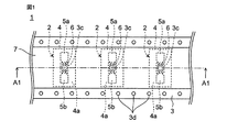
- FIG. 1 is a plan view showing a schematic configuration of a carrier tape according to an embodiment of the present invention.
- 2 is a cross-sectional view taken along line A1-A1 of FIG.
- FIG. 3 is a perspective view showing a schematic configuration of an electronic component with a sealing material.
- the carrier tape 1 is configured to accommodate a plurality of electronic components 2 with a sealing material. More specifically, the carrier tape 1 includes a tape-shaped main body 3, a plurality of sealing materials 4, a pair of terminal electrodes 5 a and 5 b, a plurality of chip-shaped electronic components 6, and a tape-shaped cover material 7. I have.
- the electronic component 2 with the sealing material includes a sealing material 4, a pair of terminal electrodes 5 a and 5 b, and an electronic component 6.
- the tape-shaped main body 3 has one main surface 3a and the other main surface 3b. One main surface 3a and the other main surface 3b are subjected to mold release treatment.
- the tape-shaped main body 3 is provided with a plurality of receiving holes 3c penetrating from one main surface 3a to the other main surface 3b.
- the plurality of accommodation holes 3 c are provided along the longitudinal direction of the tape-shaped main body 3.
- the arrangement intervals of the accommodation holes 3c are, for example, equal intervals.
- the accommodation hole 3c has a size slightly larger than that of the electronic component 6 so that the electronic component 6 is completely accommodated in a plan view and a gap of, for example, about 0.1 to 2 mm is formed around the electronic component 6.
- the tape-shaped main body 3 is composed of a member having heat resistance and flexibility, for example.
- the thickness of the tape-shaped main body 3 is, for example, 50 to 800 ⁇ m.
- the thickness of the tape-shaped main body 3, that is, the depth of the accommodation hole 3 c is substantially the same as the thickness of the electronic component 6 or thinner than the thickness of the electronic component 6.
- the sealing material 4 is, for example, affixed to an antenna base 11 to be described later, and holds the electrical connection between the antenna element 12 which is an example of a connection object and the electronic component 6.
- the sealing material 4 has an adhesive layer 4a on one main surface.
- the adhesive layer 4 a is formed on the entire one main surface of the sealing material 4.
- the sealing material 4 is affixed to the other main surface 3b of the tape-shaped main body 3 so that the adhesive layer 4a is exposed in each accommodation hole 3c.
- the sealing material 4 is formed larger in size than the accommodation hole 3c so that the accommodation hole 3c can be completely covered.
- the sealing material 4 is comprised by the member which has heat resistance, flexibility, and elasticity, such as a polyimide, for example.
- the thickness of the sealing material 4 is, for example, 20 to 200 ⁇ m.
- the pair of terminal electrodes 5 a and 5 b are for electrically connecting the electronic component 6 and an antenna element 12 to be described later, and are formed on the adhesive layer 4 a of the sealing material 4.
- the narrow portions of the pair of terminal electrodes 5a and 5b are formed of copper foil so that they can be joined to the pair of input / output terminals of the electronic component 6 by solder.
- the wide portions of the pair of terminal electrodes 5a and 5b are electrically connected to the antenna element 12 by contact or capacitive coupling. As shown in FIG. 3, one terminal electrode 5a and the other terminal electrode 5b are arranged to face each other with a gap therebetween.
- the area other than the area where the terminal electrodes 5a and 5b are provided in the sealing material 4 is an adhesion surface to the antenna element 12 and the antenna substrate 11, but the area where the terminal electrodes 5a and 5b are provided is a non-adhesion surface. .
- a part of each of a pair of terminal electrode 5a, 5b is provided so that it may be located in the accommodation hole 3c in planar view.
- the other part of each of the pair of terminal electrodes 5 a and 5 b is provided so as to be positioned between the sealing material 4 and the tape-shaped main body 3.
- the terminal electrodes 5 a and 5 b provided on the sealing material 4 function as a wiring pattern for connecting the electronic component 6 and the antenna element 12.
- the sealing material 4 may have a capacitor pattern or an inductor pattern for matching the impedance between the electronic component 6 and the antenna element 12.
- the electronic component 6 is accommodated in the accommodation hole 3c and connected to the pair of terminal electrodes 5a and 5b.
- the electronic component 6 and the pair of terminal electrodes 5a and 5b are electrically connected by, for example, solder.
- the electronic component 6 is, for example, an RFIC chip itself or an RFIC element (a package or strap in which the RFIC chip is sealed).
- the RFIC element is, for example, an ultrathin package.
- the height (thickness) of the electronic component 6 is, for example, 50 ⁇ m to 1 mm.
- the tape-shaped cover material 7 is affixed to one main surface 3a of the tape-shaped main body 3 so as to cover the plurality of housing holes 3c for housing the electronic component 6.
- One surface of the tape-like cover material 7 has a weak viscosity so that it can be easily separated even when the electronic component 6 accommodated in the accommodation hole 5c is stuck.
- the tape-shaped cover material 7 is affixed to the tape-shaped main body 3 so that the width is shorter than that of the tape-shaped main body 3 and both ends in the width direction of one main surface 3a of the tape-shaped main body 3 are exposed. At both ends in the width direction of the tape-shaped main body 3, a plurality of feed holes 3 d are provided along the longitudinal direction of the tape-shaped main body 3.
- the tape-shaped cover material 7 is made of a flexible member such as polystyrene.
- the thickness of the tape-like cover material 7 is, for example, 50 to 200 ⁇ m.
- the carrier tape since a part of each of the pair of terminal electrodes 5a and 5b is located in the accommodation hole 3c, the electronic component 6 is placed in the accommodation hole 3c using the accommodation hole 3c as a guide. Can be housed. As a result, the electronic component 6 can be positioned and connected to the pair of terminal electrodes 5a and 5b with higher accuracy. Moreover, since the several electronic component 2 with a sealing material is accommodated in the carrier tape 1, the handleability of the several electronic component 2 with a sealing material can be improved.
- the electronic component 6 is an RFIC element, but the present invention is not limited to this.
- the electronic component 6 may be a component other than the RFIC element.
- the electronic component 6 may be a sensor component such as a temperature sensor or an acceleration sensor.
- a plurality of sensor parts with a sealing material may be accommodated in a carrier tape, and the sensor parts with a sealing material may be attached to an article that is an example of a connection object such as a transport case using the carrier tape. . Thereby, a plurality of sensor components can be mounted on the article at high speed.
- 4 to 9C are diagrams showing an example of the method for manufacturing the carrier tape according to the present embodiment.
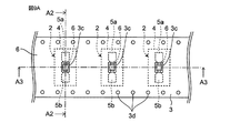
- a tape-shaped main body 3 having a plurality of receiving holes 3c penetrating from one main surface 3a to the other main surface 3b in the longitudinal direction is prepared.
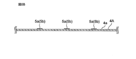
- a tape-shaped sealing material 4A having an adhesive layer 4a on one main surface and having a plurality of pairs of terminal electrodes 5a and 5b on the adhesive layer 4a is prepared.
- the tape-shaped sealing material 4 ⁇ / b> A is the same material as the sealing material 4.
- the order which prepares the tape-shaped main body 3 and the tape-shaped sealing material 4A is not limited.
- the adhesive layer 4 a of the tape-shaped sealing material 4 ⁇ / b> A is attached to the tape-shaped main body 3 so that a part of each of the pair of terminal electrodes 5 a, 5 b is located in each housing hole 3 c in plan view.
- the other main surface 3b is affixed.
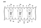
- a cut 4c is formed in the tape-shaped sealing material 4A so as to separate a portion to be the sealing material 4 including a portion overlapping with each accommodation hole 3c in plan view from the other portion 4b. . At this time, the cut extends to the other main surface 3 b of the tape-shaped main body 3.
- the other portion 4 b is separated from the tape-shaped main body 3. Since the other part 4b is connected in the longitudinal direction of the tape-shaped sealing material 4A, it can be continuously peeled off from the tape-shaped main body 3.
- the electronic component 6 is accommodated in each accommodation hole 3c of the tape-shaped main body 3, and one of each of the pair of terminal electrodes 5a, 5b located in each accommodation hole 3c. And the electronic component 6 are connected.
- connection between the pair of terminal electrodes 5a and 5b and the electronic component 6 is, for example, a heat treatment in a state where the solder 6a and 6b are disposed between the pair of terminal electrodes 5a and 5b and the electronic component 6 as shown in FIG. 9B.
- the housing hole 3c can serve as a guide to improve the self-alignment effect by the solders 6a and 6b, and the electronic component 6 can be more accurately connected to the pair of terminal electrodes 5a and 5b.
- the solder 6a and 6b may be precoated on the surface of the electronic component 6 before connection, or may be printed on a part of each of the pair of terminal electrodes 5a and 5b.
- a tape-shaped cover material 7 is attached to one main surface 3 a of the tape-shaped main body 3 so as to cover the plurality of accommodation holes 3 c that accommodate the electronic components 6.
- the sealing material 4 and the tape-shaped cover material 7 have flexibility, and the thickness of the electronic component 6 is approximately the same as or greater than the depth of the accommodation hole 3c. For this reason, the electronic component 6 is clamped between the tape-shaped cover material 7 and the pair of terminal electrodes 5a and 5b without rattling.
- the electronic component 6 since a part of each of the pair of terminal electrodes 5a and 5b is located in each accommodation hole 3c, the electronic component 6 is accommodated using the accommodation hole 3c as a guide. It can be accommodated in the hole 3c. As a result, the electronic component 6 can be positioned and connected to the pair of terminal electrodes 5a and 5b with higher accuracy.
- the handleability of the several electronic component 2 with a sealing material is improved. Can do.
- the tape-shaped cover material 7 is attached to one main surface 3a of the tape-shaped main body 3. Thereby, it can prevent that dust etc. penetrate
- the portion 4b other than the portion that becomes the sealing material 4 is separated from the tape-shaped main body 3. ing.
- the electronic component 2 with the sealing material is separated from the tape-shaped main body 3
- the electronic component 2 with the sealing material is easily separated because the portion 4 b other than the portion that becomes the sealing material 4 is removed. be able to.
- the tape-like cover material 7 is attached to one main surface 3a of the tape-like main body 3.
- the present invention is not limited to this.
- a tape-shaped main body 3 (the state shown in FIG. 9C) to which a plurality of electronic components 2 with a sealing material are attached is wound around a reel
- the other main surface 3b of the tape-shaped main body 3 adjacent inside is a tape-shaped cover material 7.
- the electronic component 6 When the tape-shaped main body 3 is wound on a reel, the electronic component 6 is pressed against the pair of terminal electrodes 5a and 5b by making the electronic component 6 thicker than the tape-shaped main body 3, and therefore the electronic component 6 and the pair of terminals The electrodes 5a and 5b can be more reliably connected.
- the portion 4b other than the portion to become the sealing material 4 is separated from the tape-shaped main body 3, but the present invention is limited to this. Not.
- the adhesiveness between the other portion 4b and the tape-shaped main body 3 so that the portion 4b other than the portion that becomes the sealing material 4 does not disturb the separation.
- the size of the cut 4c may be adjusted. Thereby, the necessity to isolate
- FIG. 10 is a perspective view showing a method for manufacturing the RFID tag 10.
- FIG. 11A is a plan view showing an antenna substrate 11 and an antenna element 12 which are parts constituting the RFID tag 10.
- 11B is a cross-sectional view taken along line A4-A4 of FIG. 11A.
- FIG. 12A is a plan view showing a state in which the electronic component 2 with the sealing material is attached on the antenna element 12.
- 12B is a cross-sectional view taken along line A5-A5 of FIG. 12A.
- the RFID tag 10 is manufactured by attaching the electronic component 2 with the sealing material to the antenna element 12 formed on one main surface of the antenna base 11.
- the RFID tag 10 is an RFID tag having a communication frequency in the 900 MHz band, for example.
- the antenna substrate 11 is composed of a flexible member such as polyethylene terephthalate (PET) or paper. On one main surface, an antenna element 12 made of copper foil, aluminum foil or silver paste is provided.
- PET polyethylene terephthalate
- an antenna element 12 made of copper foil, aluminum foil or silver paste is provided.
- the antenna element 12 includes, for example, antenna conductors 12a and 12b which are formed in a meander shape and function as a dipole antenna.
- the first end portion 12aa which is one end portion of the antenna conductor 12a and the second end portion 12ba which is one end portion of the antenna conductor 12b are arranged apart from each other.
- the interval between the first end portion 12aa and the second end portion 12ba matches or substantially matches the interval between the pair of terminal electrodes 5a and 5b.
- the sealing material 4 of the electronic component 2 with the sealing material is formed by the adhesive layer 4a so that the first end 12aa is in contact with one terminal electrode 5a and the second end 12ba is in contact with the other terminal electrode 5b. Affixed to the material 11.
- the RFID tag 10 is completed as shown in FIGS. 12A and 12B.
- the first end portion 12aa and one terminal electrode 5a, and the second end portion 12ba and the other terminal electrode 5b are in direct contact with each other without an adhesive such as the adhesive layer 4a.
- the first end portion 12aa and the one terminal electrode 5a, and the second end portion 12ba and the other terminal electrode 5b may not be directly fixed. In this case, even if the antenna substrate 11 is bent, the connecting portion between the first end portion 12aa and the one terminal electrode 5a and the connecting portion between the second end portion 12ba and the other terminal electrode 5b slide. , Stress is not concentrated here. Therefore, it can suppress that the reliability of the connection of the electronic component 2 with a sealing material and the antenna element 12 falls.
- the antenna conductors 12a and 12b are formed in a meander shape, and the tag is a UHF band RFID tag whose communication frequency band is the UHF band, but the present invention is not limited to this. .
- the antenna conductors 12a and 12b may be formed in, for example, a rectangular band shape or other shapes. Further, although the antenna conductors 12a and 12b function as dipole antennas, the present invention is not limited to this.
- the antenna conductors 12a and 12b may function as loop type antennas or may function as other types of antennas.
- the antenna element 12 may function as a spiral antenna as shown in FIG.
- the antenna element 12 is covered with a resist film except for the first end 12aa and the second end 12ba, the first end 12aa and one terminal electrode 5a, and the second end 12ba and the other end 12ba. What is necessary is just to comprise so that the terminal electrode 5b may be connected.
- an HF band RFID tag having the HF band as a communication frequency band can be configured.
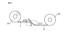
- FIG. 14 is a side view showing an example of a method for manufacturing a plurality of RFID tags 10 using the carrier tape 1.
- FIG. 15 is an enlarged cross-sectional view of a portion surrounded by a dotted line in FIG.
- a supply reel 21 around which the carrier tape 1 is wound is prepared. Also, a plurality of antenna base materials 11 on which antenna elements 12 shown in FIG. 11 are formed are connected in series to form a tape, and a supply reel 22 around which the tape is wound is prepared.
- the carrier tape 1 is continuously pulled out from the supply reel 21 and the antenna base 11 on which the antenna element 12 is formed is pulled out from the supply reel 22 to bring the carrier tape 1 and the antenna base 11 close to each other.
- the RFIC element 2 with the sealing material is separated from the tape-shaped main body 3 by bending (curving) the tape-shaped main body 3 of the carrier tape 1 in the vicinity of the antenna base 11.
- the RFIC element 2 with the sealing material is separated from the tape-shaped main body 3, and the RFIC element 2 with the sealing material is conveyed in a direction intersecting with the conveying direction of the carrier tape 1. Paste to.
- one end of the sealing material 4 is peeled off from the tape-shaped main body 3.
- One end of the sealing material 4 has an adhesive force of the adhesive layer 4a so that the other terminal electrode 5b contacts the antenna conductor 12b of the antenna element 12 conveyed in a direction crossing the conveying direction of the carrier tape 1.
- the other end of the sealing material 4 is peeled off from the tape-shaped main body 3.
- the other end of the sealing material 4 is adhered to the adhesive layer 4a so that the one terminal electrode 5a contacts the antenna conductor 12a of the antenna element 12 conveyed in a direction intersecting the conveying direction of the carrier tape 1. It sticks to the antenna substrate 11 by force.
- the RFID tag 10 shown in FIGS. 12A and 12B is manufactured. By continuously performing this operation, a plurality of RFID tags 10 can be manufactured.
- each of the pair of terminal electrodes 5a and 5b is located in each receiving hole 3c, so that the RFIC element 6 is received using the receiving hole 3c as a guide. It can be accommodated in the hole 3c. As a result, the RFIC element 6 can be positioned and connected to the pair of terminal electrodes 5a and 5b with higher accuracy. Further, since the adhesive is not applied on the pair of terminal electrodes 5a and 5b, but has the pair of terminal electrodes 5a and 5b on the adhesive layer 4a, the adhesive layer 4a is formed on the pair of terminal electrodes 5a and 5b. Not formed.
- the adhesive layer 4a is formed in a portion other than the pair of terminal electrodes 5a and 5b. Therefore, it is not necessary to apply the adhesive layer 4a with high accuracy and the amount of the adhesive is not insufficient, so that the connection reliability between the antenna element 12 and the pair of terminal electrodes 5a and 5b can be improved. .
- the RFIC element 6 with the sealing material can be separated from the tape-shaped main body 3 simply by bending the tape-shaped main body 3.
- the manufacturing cost can be reduced.
- the angle at which the tape-like main body 3 is bent and the degree of bending at the bent portion may be appropriately set in consideration of the adhesive force between the RFIC element 2 with the sealing material and the tape-like main body 3.
- the handling properties of the plurality of RFIC elements 2 with a sealing material are improved. Can do.
- the tape-like main body 3 of the drawn carrier tape 1 is separated from the supply reel 21 while the carrier tape 1 is continuously drawn from the supply reel 21. It bends at a specific position.
- the plurality of RFIC elements 2 with a sealing material are sequentially separated from the tape-shaped main body 3 and are sequentially attached to the antenna substrate 11 drawn from the supply reel 22.
- the carrier tape 1 can be pulled out at a speed of several tens of meters per minute, and the plurality of RFIC elements 6 can be separated from the tape-shaped main body 3 at a high speed.
- a plurality of RFID tags 10 can be manufactured in a shorter time.
- the sealing material 4 has a rectangular shape, and when separating the RFIC element 2 with the sealing material from the tape-shaped main body 3, it is preferable that the sealing material 4 is separated from the longitudinal portion of the sealing material 4. Thereby, the RFIC element 2 with the sealing material can be more easily separated from the tape-shaped main body 3.
- the sealing material 4 has higher rigidity than the tape-shaped main body 3. Thereby, when the tape-shaped main body 3 is bent, the sealing material 4 is easily separated from the tape-shaped main body 3. Therefore, as the sealing material 4, it is preferable to use a material or property having a larger elastic force (restoring force) such as a higher Young's modulus or a larger thickness than the tape-shaped main body 3.
- the carrier tape 1 from which the RFIC element 2 with the sealing material is separated may be wound around a take-up reel (not shown). That is, the carrier tape 1 may be conveyed by a roll-to-roll method. Similarly, the antenna substrate 11 on which the antenna element 12 is formed may be transported in a roll-to-roll manner.
- the RFIC element 2 with the sealing material separated from the tape-like main body 3 is directly attached to the antenna base material 11, but the present invention is not limited to this.
- the RFIC element 2 with the sealing material separated from the tape-shaped main body 3 may be configured to be affixed to the antenna substrate 11 using the transport device 23.
- the RFIC element 2 with the sealing material is separated from the tape-shaped main body 3 by bending the carrier tape 1 pulled out from the supply reel 21 at a specific position away from the supply reel 21.
- the separated RFIC element 2 with the sealing material is transported by the transport device 23 to the vicinity of the antenna substrate 11 pulled out from the supply reel 22.
- the one end part of the sealing material 4 adheres to the antenna base material 11 with the adhesive force of the adhesion layer 4a so that the other terminal electrode 5b may contact the antenna conductor 12b of the antenna element 12.
- the other end of the sealing material 4 is attached to the antenna base 11 by the adhesive force of the adhesive layer 4a so that the one terminal electrode 5a contacts the antenna conductor 12a of the antenna element 12.
- the adjustment of the machine is facilitated, and the RFIC element 2 with the sealing material is placed on the antenna base 11 so that the pair of terminal electrodes 5a and 5b are in contact with the first end 12aa and the second end 12ba. Can be more accurately pasted.
- the transport device 23 may be a device such as a suction head instead of a belt conveyor type device as shown in FIGS. 16 and 17. That is, the RFIC element 2 with the sealant separated from the tape-shaped main body 3 is sucked by the suction head, and the pair of terminal electrodes 5a and 5b are in contact with the first end portion 12aa and the second end portion 12ba. You may comprise so that it may affix on the base material 11.
- the present invention can connect an electronic component to a pair of terminal electrodes with higher accuracy, it is useful, for example, in manufacturing RFID tags, carrier tapes used in the manufacturing, and manufacturing methods thereof.
Landscapes
- Engineering & Computer Science (AREA)
- Microelectronics & Electronic Packaging (AREA)
- Computer Hardware Design (AREA)
- Physics & Mathematics (AREA)
- General Physics & Mathematics (AREA)
- Theoretical Computer Science (AREA)
- Mechanical Engineering (AREA)
- Packages (AREA)
- Details Of Aerials (AREA)
Abstract
一対の端子電極に対して電子部品をより精度良く接続することができるキャリアテープの製造方法を提供する。本発明に係る製造方法は、複数のシール材付き電子部品を収容するキャリアテープの製造方法であって、収容穴を長手方向に沿って複数有するテープ状本体を用意する工程と、一方の主面に形成された粘着層上に複数対の端子電極を有するテープ状シール材を用意する工程と、一対の端子電極の一部が各収容穴内に位置するように、テープ状シール材の粘着層をテープ状本体の他方の主面に貼り付ける工程と、各収容穴と重複する部分を含むシール材となる部分を他の部分から分離するようにテープ状シール材に切込みを形成する工程と、テープ状本体の各収容穴内に電子部品を収容し、各収容穴内に位置する一対の端子電極の一部と電子部品とを接続する工程とを含む。
Description
本発明は、RFID(Radio Frequency IDentifier)タグの製造方法、並びに、当該RFIDタグの製造に用いるキャリアテープ及びその製造方法に関する。
近年、物品の情報管理システムとして、リーダライタと、物品に付されたRFIDタグとを磁界や電磁界を利用した非接触方式で通信し、所定の情報を伝達するRFIDシステムが実用化されている。
RFIDタグは、アンテナ素子が形成されたアンテナ基材に、RFIC素子(RFIC(Radio Frequency Integrated Circuit)チップそのもの、またはRFICチップを搭載するパッケージ)を取り付けることによって製造される。従来、RFIC素子とアンテナ素子との接続方法として、例えば、特許文献1に記載されたものが知られている。
特許文献1において、RFIC素子は、基材上に形成された一対の端子電極(接続用導電体ともいう)に接続されている。基材は、一対の端子電極がアンテナ基材上のアンテナ素子に接続されるように、非導電性の接着剤によってアンテナ基材に貼り付けられる。これにより、RFIC素子とアンテナ素子とが一対の端子電極を介して接続され、RFIDタグが製造される。
特許文献1においては、1枚の帯状に延びるシート状の基材の全面に銅箔などの導電性箔を形成した後、エッチングなどによって導電性箔を所望の形状にパターニングすることにより複数対の端子電極を形成する。その後、各一対の端子電極にそれぞれRFIC素子を接続する。その後、シート状の基材を切断することで、一対の端子電極に接続された1個の基材付きRFIC素子を得る。この基材付きRFIC素子を接着剤を介してアンテナ基材に貼り付けることによって、RFIDタグが製造される。
この製造方法では、一対の端子電極に対して微小な電子部品であるRFIC素子を精度良く接続することが難しいという課題がある。また、基材付きRFIC素子を接着剤によってアンテナ基材に貼り付ける際、一対の端子電極とアンテナ素子との間に接着剤が介在することになる。これを避けるためには、基材上に接着剤を塗布する際に、一対の端子電極を避けて接着剤を塗布することが考えられる。しかしながら、この場合、接着剤を精度良く塗布することが難しく、接着剤の量が不足して、アンテナ素子と一対の端子電極との接続の信頼性が低下することが起こり得る。
本発明の目的は、一対の端子電極に対して電子部品をより精度良く接続することができるキャリアテープ及びその製造方法を提供することにある。また、本発明の目的は、当該キャリアテープを用いてアンテナ素子と一対の端子電極との接続の信頼性を向上させることができるRFIDタグの製造方法を提供することにある。
前記目的を達成するために、本発明の一態様に係るキャリアテープの製造方法は、
複数のシール材付き電子部品を収容するキャリアテープの製造方法であって、
一方の主面から他方の主面まで貫通する収容穴を長手方向に沿って複数有するテープ状本体を用意する工程と、
一方の主面に粘着層を有し、当該粘着層上に複数対の端子電極を有するテープ状シール材を用意する工程と、
平面視において一対の端子電極のそれぞれの一部が各収容穴内に位置するように、前記テープ状シール材の粘着層を前記テープ状本体の他方の主面に貼り付ける工程と、
平面視において各収容穴と重複する部分を含むシール材となる部分を、他の部分から分離するように前記テープ状シール材に切込みを形成する工程と、
前記テープ状本体の各収容穴内にチップ状の電子部品を収容し、各収容穴内に位置する前記一対の端子電極のそれぞれの一部と前記電子部品とを接続する工程と、
を含む。
また、本発明の一態様に係るキャリアテープは、
複数のシール材付き電子部品を収容するキャリアテープであって、
一方の主面から他方の主面まで貫通する収容穴を長手方向に沿って複数有するテープ状本体と、
一方の主面に粘着層を有するとともに当該粘着層上に一対の端子電極を有する複数のシール材であって、平面視において前記粘着層の一部及び前記一対の端子電極のそれぞれの一部が各収容穴内に位置するように、前記テープ状本体の他方の主面に貼り付けられた複数のシール材と、
各収容穴内に収容され、各収容穴内に位置する前記一対の端子電極のそれぞれの一部に接続される複数のチップ状の電子部品と、
を備える。
複数のシール材付き電子部品を収容するキャリアテープであって、
一方の主面から他方の主面まで貫通する収容穴を長手方向に沿って複数有するテープ状本体と、
一方の主面に粘着層を有するとともに当該粘着層上に一対の端子電極を有する複数のシール材であって、平面視において前記粘着層の一部及び前記一対の端子電極のそれぞれの一部が各収容穴内に位置するように、前記テープ状本体の他方の主面に貼り付けられた複数のシール材と、
各収容穴内に収容され、各収容穴内に位置する前記一対の端子電極のそれぞれの一部に接続される複数のチップ状の電子部品と、
を備える。
また、本発明の一態様に係るRFIDタグの製造方法は、
複数のシール材付きRFIC素子を収容するキャリアテープであって、一方の主面から他方の主面まで貫通する収容穴を長手方向に沿って複数有するテープ状本体と、一方の主面に粘着層を有するとともに当該粘着層上に一対の端子電極を有する複数のシール材であって、平面視において前記粘着層の一部及び前記一対の端子電極のそれぞれの一部が各収容穴内に位置するように、前記テープ状本体の他方の主面に貼り付けられた複数のシール材と、各収容穴内に収容され、各収容穴内に位置する前記一対の端子電極のそれぞれの一部に接続される複数のRFIC素子と、
を備える、キャリアテープを用意する工程と、
前記テープ状本体を折り曲げることによって、前記テープ状本体から前記シール材付きRFIC素子を分離させる工程と、
前記分離させたシール材付きRFIC素子を、前記シール材の粘着層によりアンテナ基材に貼り付ける工程と、
を含む。
本発明に係るキャリアテープ及びその製造方法によれば、一対の端子電極に対して電子部品をより精度良く接続することができる。
また、本発明に係るRFIDタグの製造方法によれば、アンテナ素子と一対の端子電極との接続の信頼性を向上させることができる。
本発明の一態様に係るキャリアテープの製造方法は、複数のシール材付き電子部品を収容するキャリアテープの製造方法であって、
一方の主面から他方の主面まで貫通する収容穴を長手方向に沿って複数有するテープ状本体を用意する工程と、
一方の主面に粘着層を有し、当該粘着層上に複数対の端子電極を有するテープ状シール材を用意する工程と、
平面視において一対の端子電極のそれぞれの一部が各収容穴内に位置するように、前記テープ状シール材の粘着層を前記テープ状本体の他方の主面に貼り付ける工程と、
平面視において各収容穴と重複する部分を含むシール材となる部分を、他の部分から分離するように前記テープ状シール材に切込みを形成する工程と、
前記テープ状本体の各収容穴内にチップ状の電子部品を収容し、各収容穴内に位置する前記一対の端子電極のそれぞれの一部と前記電子部品とを接続する工程と、
を含む。
この製造方法によれば、一対の端子電極のそれぞれの一部が各収容穴内に位置するので、当該収容穴をガイドとして電子部品が収容穴内に収容されることができる。これにより、一対の端子電極に対して電子部品をより精度良く位置決めして接続することが可能になる。例えば、はんだをプリコートした電子部品を収容穴に収容した後、加熱する。或いは、一対の端子電極のそれぞれの一部にはんだを印刷し、電子部品を収容穴に収容した後、加熱する。これらの場合、収容穴がガイドとなってはんだによるセルフアライメント効果を向上させることができ、一対の端子電極に対して電子部品をより精度良く接続することができる。また、複数のシール材付き電子部品がキャリアテープに収容されるので、複数のシール材付き電子部品の取扱い性を向上させることができる。
なお、本発明の一態様に係るキャリアテープの製造方法は、前記テープ状本体の一方の主面に、前記電子部品を収容する前記複数の収容穴を覆うようにテープ状カバー材を貼り付ける工程をさらに含んでもよい。
この製造方法によれば、電子部品を収容する収容穴に塵埃等が侵入することを防ぐことができ、一対の端子電極に対して電子部品をより精度良く接続することができる。
また、本発明の一態様に係るキャリアテープの製造方法は、前記テープ状シール材に前記切込みを形成した後、前記シール材となる部分以外の部分を前記テープ状本体から分離する工程をさらに含んでもよい。
この製造方法によれば、シール材付き電子部品をテープ状本体から分離するとき、シール材となる部分以外の部分が除去された状態で分離するので、シール材付き電子部品を容易に分離することができる。
本発明に係るキャリアテープは、複数のシール材付き電子部品を収容するキャリアテープであって、
一方の主面から他方の主面まで貫通する収容穴を長手方向に沿って複数有するテープ状本体と、
一方の主面に粘着層を有するとともに当該粘着層上に一対の端子電極を有する複数のシール材であって、平面視において前記粘着層の一部及び前記一対の端子電極のそれぞれの一部が各収容穴内に位置するように、前記テープ状本体の他方の主面に貼り付けられた複数のシール材と、
各収容穴内に収容され、各収容穴内に位置する前記シール材の粘着層の一部に貼り付けられるとともに、各収容穴内に位置する前記一対の端子電極のそれぞれの一部に接続される複数のチップ状の電子部品と、
を備える。
一方の主面から他方の主面まで貫通する収容穴を長手方向に沿って複数有するテープ状本体と、
一方の主面に粘着層を有するとともに当該粘着層上に一対の端子電極を有する複数のシール材であって、平面視において前記粘着層の一部及び前記一対の端子電極のそれぞれの一部が各収容穴内に位置するように、前記テープ状本体の他方の主面に貼り付けられた複数のシール材と、
各収容穴内に収容され、各収容穴内に位置する前記シール材の粘着層の一部に貼り付けられるとともに、各収容穴内に位置する前記一対の端子電極のそれぞれの一部に接続される複数のチップ状の電子部品と、
を備える。
このキャリアテープによれば、一対の端子電極のそれぞれの一部が収容穴内に位置するので、当該収容穴をガイドとして電子部品が収容穴内に収容されることができる。これにより、一対の端子電極に対して電子部品をより精度良く位置決めして接続することが可能になる。また、複数のシール材付き電子部品がキャリアテープに収容されるので、複数のシール材付き電子部品の取扱い性を向上させることができる。
なお、前記シール材は、前記テープ状本体よりも剛性が高いことが好ましい。これにより、テープ状本体を折り曲げたときに、シール材がテープ状本体から分離し易くなる。
なお、前記電子部品は、RFIC素子であってもよい。
本発明の一態様に係るRFIDタグの製造方法は、
複数のシール材付きRFIC素子を収容するキャリアテープであって、一方の主面から他方の主面まで貫通する収容穴を長手方向に沿って複数有するテープ状本体と、一方の主面に粘着層を有するとともに当該粘着層上に一対の端子電極を有する複数のシール材であって、平面視において前記粘着層の一部及び前記一対の端子電極のそれぞれの一部が各収容穴内に位置するように、前記テープ状本体の他方の主面に貼り付けられた複数のシール材と、各収容穴内に収容され、各収容穴内に位置する前記シール材の粘着層の一部に貼り付けられるとともに、各収容穴内に位置する前記一対の端子電極のそれぞれの一部に接続される複数のRFIC素子と、
を備える、キャリアテープを用意する工程と、
前記テープ状本体を折り曲げることによって、前記テープ状本体から前記シール材付きRFIC素子を分離させる工程と、
前記分離させたシール材付きRFIC素子を、前記シール材の粘着層によりアンテナ基材に貼り付ける工程と、
を含む。
この製造方法によれば、一対の端子電極のそれぞれの一部が各収容穴内に位置するので、当該収容穴をガイドとしてRFIC素子が収容穴内に収容されることができる。これにより、一対の端子電極に対してRFIC素子をより精度良く位置決めして接続することが可能になる。また、一対の端子電極上に接着剤を塗布するのではなく、粘着層上に一対の端子電極を有するので、一対の端子電極上には粘着層が形成されない一方で、一対の端子電極以外の部分には粘着層が形成されることになる。従って、粘着層を精度良く塗布する必要性がなく、接着剤の量が不足することもないので、アンテナ素子と一対の端子電極との接続の信頼性を向上させることができる。また、テープ状本体を折り曲げるだけで、テープ状本体からシール材付きRFIC素子を分離させることができるので、製造工程の短縮及び製造コストの削減を図ることができる。
なお、前記キャリアテープは、供給リールに巻き回され、
前記複数のシール材付きRFIC素子は、前記供給リールから前記キャリアテープを連続的に引き出しながら、当該引き出された前記キャリアテープの前記テープ状本体を、前記供給リールから離れた特定の位置で折り曲げることにより、前記テープ状本体から逐次分離されるようにしてもよい。
前記複数のシール材付きRFIC素子は、前記供給リールから前記キャリアテープを連続的に引き出しながら、当該引き出された前記キャリアテープの前記テープ状本体を、前記供給リールから離れた特定の位置で折り曲げることにより、前記テープ状本体から逐次分離されるようにしてもよい。
この製造方法によれば、複数のRFIC素子をテープ状本体から高速で分離させることができる。その結果、複数のRFIDタグをより短時間で製造することが可能になる。
なお、前記シール材は、平面視において長手方向と短手方向を有する形状(例えば、矩形状)を有し、前記シール材付きRFIC素子を前記テープ状本体から分離させるとき、前記シール材の長手方向の部分から分離させることが好ましい。これにより、シール材付きRFIC素子をテープ状本体から、より容易に分離させることができる。
以下、本発明の実施形態について、図面を参照しながら説明する。
(実施の形態)
図1は、本発明の実施の形態に係るキャリアテープの概略構成を示す平面図である。図2は、図1のA1-A1線断面図である。図3は、シール材付き電子部品の概略構成を示す斜視図である。
図1は、本発明の実施の形態に係るキャリアテープの概略構成を示す平面図である。図2は、図1のA1-A1線断面図である。図3は、シール材付き電子部品の概略構成を示す斜視図である。
図1又は図2に示すように、本実施の形態に係るキャリアテープ1は、複数のシール材付き電子部品2を収容するように構成されている。より具体的には、キャリアテープ1は、テープ状本体3と、複数のシール材4と、一対の端子電極5a,5bと、複数のチップ状の電子部品6と、テープ状カバー材7とを備えている。シール材付き電子部品2は、シール材4と、一対の端子電極5a,5bと、電子部品6とにより構成されている。
テープ状本体3は、一方の主面3aと、他方の主面3bとを有している。一方の主面3a及び他方の主面3bには、離型処理が施されている。テープ状本体3には、一方の主面3aから他方の主面3bまで貫通する複数の収容穴3cが設けられている。複数の収容穴3cは、テープ状本体3の長手方向に沿って設けられている。収容穴3cの配置間隔は、例えば、等間隔である。収容穴3cは、平面視において電子部品6を完全に収容するとともに、電子部品6の周囲に例えば0.1~2mm程度の隙間が空くように、電子部品6よりもやや大きなサイズを有する。ここで、「平面視」とは、図1に示す方向から見た状態をいう。テープ状本体3は、例えば、耐熱性及び可撓性を有する部材で構成されている。テープ状本体3の厚さは、例えば、50~800μmである。テープ状本体3の厚さ、つまり収容穴3cの深さは、電子部品6の厚みとほぼ同じか、電子部品6の厚みよりも薄い。
シール材4は、例えば、後述するアンテナ基材11に貼り付けられ、接続対象物の一例であるアンテナ素子12と電子部品6との電気的接続を保持するものである。シール材4は、一方の主面に粘着層4aを有している。粘着層4aは、例えば、シール材4の一方の主面の全体に形成されている。シール材4は、各収容穴3cに粘着層4aが露出するように、テープ状本体3の他方の主面3bに貼り付けられている。本実施の形態において、シール材4は、収容穴3cを完全に覆うことができるように、収容穴3cよりもサイズが大きく形成されている。シール材4は、例えば、ポリイミドなどの耐熱性、可撓性、及び弾性を有する部材により構成されている。シール材4の厚さは、例えば、20~200μmである。
一対の端子電極5a,5bは、電子部品6と後述するアンテナ素子12とを電気的に接続するものであり、シール材4の粘着層4a上に形成されている。一対の端子電極5a,5bのうち各幅狭部は、電子部品6の一対の入出力端子に対してはんだにより接合できるように、銅箔により形成されている。一対の端子電極5a,5bのうち各幅広部は、アンテナ素子12に対して接触または容量結合により電気的に接続される。一方の端子電極5aと他方の端子電極5bとは、図3に示すように、互いに隙間を空けて対向するように配置されている。つまり、シール材4のうち端子電極5a,5bが設けられた領域以外はアンテナ素子12およびアンテナ基材11に対する接着面であるが、端子電極5a,5bが設けられた領域は非接着面である。また、一対の端子電極5a,5bのそれぞれの一部は、図1に示すように、平面視において収容穴3c内に位置するように設けられている。一対の端子電極5a,5bのそれぞれの他部は、シール材4とテープ状本体3との間に位置するように設けられている。なお、本実施の形態において、シール材4に設けた端子電極5a,5bは、電子部品6とアンテナ素子12とを接続するための配線パターンとして機能する。シール材4は、当該配線パターンの他、電子部品6とアンテナ素子12とのインピーダンスを整合させるためのキャパシタパターンやインダクタパターンを有してもよい。
電子部品6は、収容穴3c内に収容され、一対の端子電極5a,5bに接続されている。電子部品6と一対の端子電極5a,5bとは、例えば、はんだにより電気的に接続されている。本実施の形態において、電子部品6は、例えば、RFICチップそのもの又はRFIC素子(RFICチップを封止したパッケージやストラップ)である。RFIC素子は、例えば、極薄パッケージ(ultrathin package)である。電子部品6の高さ(厚さ)は、例えば、50μm~1mmである。
テープ状カバー材7は、電子部品6を収容する複数の収容穴3cを覆うように、テープ状本体3の一方の主面3aに貼り付けられている。テープ状カバー材7の一方の面は、収容穴5cに収容された電子部品6が貼り付いた場合でも容易に分離できるように、弱粘性を有している。テープ状カバー材7は、テープ状本体3よりも幅が短く、テープ状本体3の一方の主面3aの幅方向の両端部が露出するように、テープ状本体3に貼り付けられている。テープ状本体3の幅方向の両端部には、テープ状本体3の長手方向に沿って複数の送り穴3dが設けられている。テープ状カバー材7は、例えば、ポリスチレンなどの可撓性を有する部材で構成されている。テープ状カバー材7の厚さは、例えば、50~200μmである。
本実施の形態に係るキャリアテープによれば、一対の端子電極5a,5bのそれぞれの一部が収容穴3c内に位置するので、当該収容穴3cをガイドとして電子部品6が収容穴3c内に収容されることができる。これにより、一対の端子電極5a,5bに対して電子部品6をより精度良く位置決めして接続することが可能になる。また、複数のシール材付き電子部品2がキャリアテープ1に収容されるので、複数のシール材付き電子部品2の取扱い性を向上させることができる。
なお、本実施の形態において、電子部品6はRFIC素子であるとしたが、本発明はこれに限定されない。シール材付き電子部品2を、RFIDタグの製造とは異なる用途に使用する場合、電子部品6はRFIC素子以外の部品であってもよい。例えば、電子部品6は、温度センサや加速度センサ等のセンサ部品であってもよい。この場合、複数のシール材付きセンサ部品をキャリアテープに収容し、当該キャリアテープを用いてシール材付きセンサ部品を搬送用ケース等の接続対象物の一例である物品に貼付けるようにすればよい。これにより、複数のセンサ部品を物品上に高速に搭載することができる。
次に、本実施の形態に係るキャリアテープの製造方法について説明する。図4~図9Cは、本実施の形態に係るキャリアテープの製造方法の一例を示す図である。
まず、図4に示すように、一方の主面3aから他方の主面3bまで貫通する収容穴3cを長手方向に沿って複数有するテープ状本体3を用意する。
また、図5A及び図5Bに示すように、一方の主面に粘着層4aを有し、当該粘着層4a上に複数対の端子電極5a,5bを有するテープ状シール材4Aを用意する。テープ状シール材4Aは、シール材4と同じ材質である。なお、テープ状本体3及びテープ状シール材4Aを用意する順序は限定されない。
次いで、図6に示すように、平面視において一対の端子電極5a,5bのそれぞれの一部が各収容穴3c内に位置するように、テープ状シール材4Aの粘着層4aをテープ状本体3の他方の主面3bに貼り付ける。
次いで、図7に示すように、平面視において各収容穴3cと重複する部分を含むシール材4となる部分を、他の部分4bから分離するようにテープ状シール材4Aに切込み4cを形成する。このとき、該切込みはテープ状本体3の他方の主面3bにも及ぶ。
次いで、図8A及び図8Bに示すように、他の部分4bをテープ状本体3から分離する。他の部分4bはテープ状シール材4Aの長手方向に繋がっているので、連続的にテープ状本体3から引き剥がすことができる。
次いで、図9A~図9Cに示すように、テープ状本体3の各収容穴3c内に電子部品6を収容するとともに、各収容穴3c内に位置する一対の端子電極5a,5bのそれぞれの一部と電子部品6とを接続する。
一対の端子電極5a,5bと電子部品6との接続は、例えば、図9Bに示すように、一対の端子電極5a,5bと電子部品6との間にはんだ6a,6bを配置した状態で熱処理することにより行うことができる。この場合、収容穴3cがガイドとなってはんだ6a,6bによるセルフアライメント効果を向上させることができ、一対の端子電極5a,5bに対して電子部品6をより精度良く接続することができる。なお、はんだ6a,6bは、接続前において、電子部品6の表面にプリコートされてもよいし、一対の端子電極5a,5bのそれぞれの一部に印刷されてもよい。
次いで、図2に示すように、テープ状本体3の一方の主面3aに、電子部品6を収容する複数の収容穴3cを覆うようにテープ状カバー材7を貼り付ける。シール材4及びテープ状カバー材7が可撓性を有しており、電子部品6の厚みは、収容穴3cの深さとほぼ同じ又はそれ以上である。このため、電子部品6は、テープ状カバー材7と一対の端子電極5a,5bとの間でガタつきなく挟持される。
本実施の形態に係るキャリアテープの製造方法によれば、一対の端子電極5a,5bのそれぞれの一部が各収容穴3c内に位置するので、当該収容穴3cをガイドとして電子部品6が収容穴3c内に収容されることができる。これにより、一対の端子電極5a,5bに対して電子部品6をより精度良く位置決めして接続することが可能になる。
また、本実施の形態に係るキャリアテープの製造方法によれば、複数のシール材付き電子部品2がキャリアテープ1に収容されるので、複数のシール材付き電子部品2の取扱い性を向上させることができる。
また、本実施の形態に係るキャリアテープの製造方法によれば、テープ状本体3の一方の主面3aにテープ状カバー材7を貼り付けるようにしている。これにより、電子部品6を収容する収容穴3cに塵埃等が侵入することを防ぐことができ、一対の端子電極5a,5bに対して電子部品6をより精度良く接続することができる。
また、本実施の形態に係るキャリアテープの製造方法によれば、テープ状シール材4Aに切込み4cを形成した後、シール材4となる部分以外の部分4bをテープ状本体3から分離するようにしている。これにより、シール材付き電子部品2をテープ状本体3から分離するとき、シール材4となる部分以外の部分4bが除去された状態で分離するので、シール材付き電子部品2を容易に分離することができる。
なお、本実施の形態では、テープ状本体3の一方の主面3aにテープ状カバー材7を貼り付けるようにしたが、本発明はこれに限定されない。例えば、複数のシール材付き電子部品2が取り付いたテープ状本体3(図9Cに示す状態)をリールに巻くと、内側で隣接するテープ状本体3の他方の主面3bがテープ状カバー材7の機能を果たすことができる。このような場合、テープ状カバー材7を不要とすることができる。このテープ状本体3をリールに巻く場合、電子部品6をテープ状本体3より厚い状態にすることで、電子部品6が一対の端子電極5a,5bに押し付けられるので、電子部品6と一対の端子電極5a,5bとをより確実に接続することができる。
また、本実施の形態では、テープ状シール材4Aに切込み4cを形成した後、シール材4となる部分以外の部分4bをテープ状本体3から分離するようにしたが、本発明はこれに限定されない。シール材付き電子部品2をテープ状本体3から分離するときに、シール材4となる部分以外の部分4bが当該分離を妨げないように、当該他の部分4bとテープ状本体3との粘着性や切込み4cのサイズ等を調整してもよい。これにより、他の部分4bをテープ状本体3から分離する必要性を無くすことができる。
次に、シール材付き電子部品であるシール材付きRFIC素子2を用いて、RFIDタグ10を製造する方法について説明する。図10は、RFIDタグ10の製造方法を示す斜視図である。図11Aは、RFIDタグ10を構成する部品であるアンテナ基材11及びアンテナ素子12を示す平面図である。図11Bは、図11AのA4-A4線断面図である。図12Aは、アンテナ素子12上にシール材付き電子部品2を取り付けた状態を示す平面図である。図12Bは、図12AのA5-A5線断面図である。
図10~図12Bに示すように、RFIDタグ10は、シール材付き電子部品2がアンテナ基材11の一方の主面に形成されたアンテナ素子12に取り付けられることにより製造される。RFIDタグ10は、例えば、900MHz帯を通信周波数とするRFIDタグである。
アンテナ基材11は、ポリエチレンテレフタレート(PET)や紙などの可撓性を有する部材で構成されている。一方の主面には銅箔やアルミ箔又は銀ペーストによるアンテナ素子12が設けられている。
アンテナ素子12は、例えば、ミアンダ状に形成され、ダイポール型のアンテナとして機能するアンテナ導体12a,12bを備えている。アンテナ導体12aの一端部である第1端部12aaと、アンテナ導体12bの一端部である第2端部12baとは、互いに離れて配置されている。第1端部12aaと第2端部12baの間隔は、一対の端子電極5a,5bとの間隔と一致又は略一致する。
シール材付き電子部品2のシール材4は、第1端部12aaが一方の端子電極5aに接触し、第2端部12baが他方の端子電極5bに接触するように、粘着層4aによりアンテナ基材11に貼り付けられる。これにより、図12A及び図12Bに示すように、RFIDタグ10が完成する。このとき、第1端部12aaと一方の端子電極5a、並びに、第2端部12baと他方の端子電極5bとは、粘着層4aなどの接着剤を介さず直接接触する。
なお、第1端部12aaと一方の端子電極5a、並びに、第2端部12baと他方の端子電極5bとは、直接固定されなくてもよい。この場合、アンテナ基材11が撓んでも、第1端部12aaと一方の端子電極5aとの接続部、並びに、第2端部12baと他方の端子電極5bとの接続部が摺動するため、ここに応力が集中することはない。従って、シール材付き電子部品2とアンテナ素子12との接続の信頼性が低下することを抑えることができる。
なお、本実施の形態では、アンテナ導体12a,12bは、ミアンダ状に形成されるものであり、タグはUHF帯を通信周波数帯とするUHF帯RFIDタグとしたが、本発明はこれに限定されない。アンテナ導体12a,12bは、例えば、矩形帯状に形成されても、他の形状に形成されてもよい。また、アンテナ導体12a,12bは、ダイポール型のアンテナとして機能するものとしたが、本発明はこれに限定されない。アンテナ導体12a,12bは、ループ型のアンテナとして機能するものであっても、その他の型のアンテナとして機能するものであってもよい。また、アンテナ素子12は、図13に示すように、螺旋状のアンテナとして機能するものであってもよい。この場合、例えば、第1端部12aa及び第2端部12baを除いてアンテナ素子12をレジスト膜で覆い、第1端部12aaと一方の端子電極5a、及び、第2端部12baと他方の端子電極5bとを接続するように構成すればよい。これにより、HF帯を通信周波数帯とするHF帯RFIDタグを構成できる。
次に、キャリアテープ1を用いて複数のRFIDタグ10を製造する方法について説明する。図14は、キャリアテープ1を用いて複数のRFIDタグ10を製造する方法の一例を示す側面図である。図15は、図14の点線で囲んだ部分の拡大断面図である。
まず、図14に示すように、キャリアテープ1を巻き回した供給リール21を用意する。また、図11に示すアンテナ素子12が形成されたアンテナ基材11を複数直列につないでテープ状に形成し、それを巻き回した供給リール22を用意する。
次いで、供給リール21からキャリアテープ1を連続的に引き出すとともに、供給リール22からアンテナ素子12が形成されたアンテナ基材11を引き出し、キャリアテープ1とアンテナ基材11とを接近させる。
次いで、図15に示すように、アンテナ基材11の近傍でキャリアテープ1のテープ状本体3を折り曲げる(湾曲させる)ことによって、テープ状本体3からシール材付きRFIC素子2を分離させる。この分離の際に、シール材付きRFIC素子2がテープ状本体3から分離しながら、シール材付きRFIC素子2を、キャリアテープ1の搬送方向に対して交差する方向に搬送されるアンテナ基材11に貼り付ける。
より具体的には、アンテナ基材11の近傍でキャリアテープ1のテープ状本体3を折り曲げることによって、まず、シール材4の一端部がテープ状本体3から剥離する。このシール材4の一端部は、キャリアテープ1の搬送方向に対して交差する方向に搬送されるアンテナ素子12のアンテナ導体12bに他方の端子電極5bが接触するように、粘着層4aの粘着力によりアンテナ基材11に貼り付く。その後、キャリアテープ1及びアンテナ素子12の移動が進むことで、シール材4の他端部がテープ状本体3から剥離する。このシール材4の他端部は、キャリアテープ1の搬送方向に対して交差する方向に搬送されるアンテナ素子12のアンテナ導体12aに一方の端子電極5aが接触するように、粘着層4aの粘着力によりアンテナ基材11に貼り付く。これにより、図12A及び図12Bに示すRFIDタグ10が製造される。この動作を連続的に行うことにより、複数のRFIDタグ10を製造することができる。
本実施の形態に係るRFIDタグの製造方法によれば、一対の端子電極5a,5bのそれぞれの一部が各収容穴3c内に位置するので、当該収容穴3cをガイドとしてRFIC素子6が収容穴3c内に収容されることができる。これにより、一対の端子電極5a,5bに対してRFIC素子6をより精度良く位置決めして接続することが可能になる。また、一対の端子電極5a,5b上に接着剤を塗布するのではなく、粘着層4a上に一対の端子電極5a,5bを有するので、一対の端子電極5a,5b上には粘着層4aが形成されない。一方、一対の端子電極5a,5b以外の部分には粘着層4aが形成されることになる。従って、粘着層4aを精度良く塗布する必要性がなく、接着剤の量が不足することもないので、アンテナ素子12と一対の端子電極5a,5bとの接続の信頼性を向上させることができる。
また、本実施の形態に係るRFIDタグの製造方法によれば、テープ状本体3を折り曲げるだけで、テープ状本体3からシール材付きRFIC素子6を分離させることができるので、製造工程の短縮及び製造コストの削減を図ることができる。なお、テープ状本体3を折り曲げる角度及び折り曲げ箇所における湾曲の度合は、シール材付きRFIC素子2とテープ状本体3との接着力等を考慮して適宜設定すればよい。
また、本実施の形態に係るRFIDタグの製造方法によれば、複数のシール材付きRFIC素子2がキャリアテープ1に収容されるので、複数のシール材付きRFIC素子2の取扱い性を向上させることができる。
また、本実施の形態に係るRFIDタグの製造方法によれば、供給リール21からキャリアテープ1を連続的に引き出しながら、当該引き出されたキャリアテープ1のテープ状本体3を、供給リール21から離れた特定の位置で折り曲げるようにしている。これにより、複数のシール材付きRFIC素子2をテープ状本体3から逐次分離し、供給リール22から引き出されるアンテナ基材11に逐次貼り付けるようにしている。これにより、例えば、キャリアテープ1を毎分数10mの速度で引き出し、複数のRFIC素子6をテープ状本体3から高速で分離させることができる。その結果、複数のRFIDタグ10をより短時間で製造することが可能になる。
なお、シール材4は、矩形状を有し、シール材付きRFIC素子2をテープ状本体3から分離させるとき、シール材4の長手方向の部分から分離させることが好ましい。これにより、シール材付きRFIC素子2をテープ状本体3から、より容易に分離させることができる。
また、シール材4は、テープ状本体3よりも剛性が高いことが好ましい。これにより、テープ状本体3を折り曲げたときに、シール材4がテープ状本体3から分離し易くなる。よって、シール材4としては、テープ状本体3よりも、ヤング率がより大きい、厚みがより厚いなど、弾性力(復元力)のより大きな材質や性状のものを用いることが好ましい。
また、シール材付きRFIC素子2が分離されたキャリアテープ1は、巻き取りリール(図示せず)に巻き取られるようにしてもよい。すなわち、キャリアテープ1は、ロールツーロール方式で搬送されるようにしてもよい。同様に、アンテナ素子12が形成されたアンテナ基材11も、ロールツーロール方式で搬送されるようにしてもよい。
なお、図14及び図15に示す製造例では、テープ状本体3から分離したシール材付きRFIC素子2を直接的にアンテナ基材11に貼り付けるようにしたが、本発明はこれに限定されない。例えば、図16及び図17に示すように、テープ状本体3から分離したシール材付きRFIC素子2を、搬送装置23を用いてアンテナ基材11に貼り付けるように構成してもよい。
より具体的には、供給リール21から引き出したキャリアテープ1を、供給リール21から離れた特定の位置で折り曲げることにより、テープ状本体3からシール材付きRFIC素子2を分離させる。当該分離させたシール材付きRFIC素子2を、搬送装置23により、供給リール22から引き出したアンテナ基材11の近傍に搬送する。これにより、アンテナ素子12のアンテナ導体12bに他方の端子電極5bが接触するように、シール材4の一端部が粘着層4aの粘着力によりアンテナ基材11に貼り付く。また、アンテナ素子12のアンテナ導体12aに一方の端子電極5aが接触するように、シール材4の他端部が粘着層4aの粘着力によりアンテナ基材11に貼り付く。この動作を連続的に行うことにより、複数のRFIDタグ10を製造することができる。
この構成によれば、機械の調整が容易になり、一対の端子電極5a,5bが第1端部12aa,第2端部12baに接触するように、シール材付きRFIC素子2をアンテナ基材11に、より正確に貼り付けることができる。
なお、搬送装置23は、図16及び図17に示すようなベルトコンベア形式の装置ではなく、吸着ヘッドのような装置であってもよい。すなわち、テープ状本体3から分離されたシール材付きRFIC素子2を吸着ヘッドにより吸着して、一対の端子電極5a,5bが第1端部12aa,第2端部12baに接触するように、アンテナ基材11に貼り付けるように構成してもよい。
本発明は、添付図面を参照しながら好ましい実施の形態に関連して充分に記載されているが、この技術に熟練した人々にとっては種々の変形や修正は明白である。そのような変形や修正は、添付した請求の範囲による本発明の範囲から外れない限りにおいて、その中に含まれると理解されるべきである。
本発明は、一対の端子電極に対して電子部品をより精度良く接続することができるので、例えば、RFIDタグの製造、並びに当該製造に使用されるキャリアテープ及びその製造方法に有用である。
1 キャリアテープ
2 シール材付き電子部品(シール材付きRFIC素子)
3 テープ状本体
3a 一方の主面
3b 他方の主面
3c 収容穴
3d 送り穴
4 シール材
4A テープ状シール材
4a 粘着層
4b 他の部分
4c 切込み
5a,5b 端子電極
6 電子部品(RFIC素子)
6a,6b はんだ
7 テープ状カバー材
10 RFIDタグ
11 アンテナ基材
12 アンテナ素子
12a,12b アンテナ導体
12aa 第1端部
12ba 第2端部
21,22 供給リール
23 搬送装置
2 シール材付き電子部品(シール材付きRFIC素子)
3 テープ状本体
3a 一方の主面
3b 他方の主面
3c 収容穴
3d 送り穴
4 シール材
4A テープ状シール材
4a 粘着層
4b 他の部分
4c 切込み
5a,5b 端子電極
6 電子部品(RFIC素子)
6a,6b はんだ
7 テープ状カバー材
10 RFIDタグ
11 アンテナ基材
12 アンテナ素子
12a,12b アンテナ導体
12aa 第1端部
12ba 第2端部
21,22 供給リール
23 搬送装置
Claims (9)
- 複数のシール材付き電子部品を収容するキャリアテープの製造方法であって、
一方の主面から他方の主面まで貫通する収容穴を長手方向に沿って複数有するテープ状本体を用意する工程と、
一方の主面に粘着層を有し、当該粘着層上に複数対の端子電極を有するテープ状シール材を用意する工程と、
平面視において一対の端子電極のそれぞれの一部が各収容穴内に位置するように、前記テープ状シール材の粘着層を前記テープ状本体の他方の主面に貼り付ける工程と、
平面視において各収容穴と重複する部分を含むシール材となる部分を、他の部分から分離するように前記テープ状シール材に切込みを形成する工程と、
前記テープ状本体の各収容穴内にチップ状の電子部品を収容し、各収容穴内に位置する前記一対の端子電極のそれぞれの一部と前記電子部品とを接続する工程と、
を含む、キャリアテープの製造方法。 - 前記テープ状本体の一方の主面に、前記電子部品を収容する前記複数の収容穴を覆うようにテープ状カバー材を貼り付ける工程をさらに含む、請求項1に記載のキャリアテープの製造方法。
- 前記テープ状シール材に前記切込みを形成した後、前記シール材となる部分以外の部分を前記テープ状本体から分離する工程をさらに含む、請求項1又は2に記載のキャリアテープの製造方法。
- 複数のシール材付き電子部品を収容するキャリアテープであって、
一方の主面から他方の主面まで貫通する収容穴を長手方向に沿って複数有するテープ状本体と、
一方の主面に粘着層を有するとともに当該粘着層上に一対の端子電極を有する複数のシール材であって、平面視において前記粘着層の一部及び前記一対の端子電極のそれぞれの一部が各収容穴内に位置するように、前記テープ状本体の他方の主面に貼り付けられた複数のシール材と、
各収容穴内に収容され、各収容穴内に位置する前記一対の端子電極のそれぞれの一部に接続される複数のチップ状の電子部品と、
を備える、キャリアテープ。 - 前記シール材は、前記テープ状本体よりも剛性が高い、請求項4に記載のキャリアテープ。
- 前記電子部品は、RFIC素子である、請求項4又は5に記載のキャリアテープ。
- 複数のシール材付きRFIC素子を収容するキャリアテープであって、一方の主面から他方の主面まで貫通する収容穴を長手方向に沿って複数有するテープ状本体と、一方の主面に粘着層を有するとともに当該粘着層上に一対の端子電極を有する複数のシール材であって、平面視において前記粘着層の一部及び前記一対の端子電極のそれぞれの一部が各収容穴内に位置するように、前記テープ状本体の他方の主面に貼り付けられた複数のシール材と、各収容穴内に収容され、各収容穴内に位置する前記一対の端子電極のそれぞれの一部に接続される複数のRFIC素子と、
を備える、キャリアテープを用意する工程と、
前記テープ状本体を折り曲げることによって、前記テープ状本体から前記シール材付きRFIC素子を分離させる工程と、
前記分離させたシール材付きRFIC素子を、前記シール材の粘着層によりアンテナ基材に貼り付ける工程と、
を含む、RFIDタグの製造方法。 - 前記キャリアテープは、供給リールに巻き回され、
前記複数のシール材付きRFIC素子は、前記供給リールから前記キャリアテープを連続的に引き出しながら、当該引き出された前記キャリアテープの前記テープ状本体を、前記供給リールから離れた特定の位置で折り曲げることにより、前記テープ状本体から逐次分離される、請求項7に記載のRFIDタグの製造方法。 - 前記シール材は、平面視において長手方向と短手方向を有し、
前記シール材付きRFIC素子を前記テープ状本体から分離させるとき、前記シール材の長手方向の部分から分離させる、請求項7又は8に記載のRFIDタグの製造方法。
Priority Applications (3)
| Application Number | Priority Date | Filing Date | Title |
|---|---|---|---|
| JP2017534619A JP6206626B1 (ja) | 2016-04-11 | 2017-03-22 | キャリアテープ及びその製造方法、並びにrfidタグの製造方法 |
| CN201780021495.8A CN109074507B (zh) | 2016-04-11 | 2017-03-22 | 载带及其制造方法、以及rfid标签的制造方法 |
| US16/124,393 US10360492B2 (en) | 2016-04-11 | 2018-09-07 | Carrier tape, method for manufacturing same, and method for manufacturing RFID tag |
Applications Claiming Priority (2)
| Application Number | Priority Date | Filing Date | Title |
|---|---|---|---|
| JP2016079046 | 2016-04-11 | ||
| JP2016-079046 | 2016-04-11 |
Related Child Applications (1)
| Application Number | Title | Priority Date | Filing Date |
|---|---|---|---|
| US16/124,393 Continuation US10360492B2 (en) | 2016-04-11 | 2018-09-07 | Carrier tape, method for manufacturing same, and method for manufacturing RFID tag |
Publications (1)
| Publication Number | Publication Date |
|---|---|
| WO2017179380A1 true WO2017179380A1 (ja) | 2017-10-19 |
Family
ID=60042478
Family Applications (1)
| Application Number | Title | Priority Date | Filing Date |
|---|---|---|---|
| PCT/JP2017/011427 WO2017179380A1 (ja) | 2016-04-11 | 2017-03-22 | キャリアテープ及びその製造方法、並びにrfidタグの製造方法 |
Country Status (4)
| Country | Link |
|---|---|
| US (1) | US10360492B2 (ja) |
| JP (1) | JP6418298B2 (ja) |
| CN (1) | CN109074507B (ja) |
| WO (1) | WO2017179380A1 (ja) |
Families Citing this family (2)
| Publication number | Priority date | Publication date | Assignee | Title |
|---|---|---|---|---|
| USD876963S1 (en) * | 2018-03-30 | 2020-03-03 | Advantek, Inc. | Carrier tape |
| CN114030668B (zh) * | 2021-11-24 | 2022-12-27 | 乐清市嘉得电子有限公司 | 一种端子编带机的自动穿签机构 |
Citations (5)
| Publication number | Priority date | Publication date | Assignee | Title |
|---|---|---|---|---|
| WO2006112447A1 (ja) * | 2005-04-18 | 2006-10-26 | Hallys Corporation | 電子部品及び、この電子部品の製造方法 |
| JP2010055467A (ja) * | 2008-08-29 | 2010-03-11 | Toppan Printing Co Ltd | 光学機能付きrfidラベル |
| WO2010140429A1 (ja) * | 2009-06-03 | 2010-12-09 | 株式会社村田製作所 | 無線icデバイス及びその製造方法 |
| JP5904316B1 (ja) * | 2014-11-07 | 2016-04-13 | 株式会社村田製作所 | キャリアテープ及びその製造方法、並びにrfidタグの製造方法 |
| JP6057042B1 (ja) * | 2015-06-18 | 2017-01-11 | 株式会社村田製作所 | キャリアテープ及びその製造方法、並びにrfidタグの製造方法 |
Family Cites Families (10)
| Publication number | Priority date | Publication date | Assignee | Title |
|---|---|---|---|---|
| JPS6482603A (en) * | 1987-09-25 | 1989-03-28 | Alps Electric Co Ltd | Method of sticking cover to electronic component |
| JPH1134557A (ja) * | 1997-07-24 | 1999-02-09 | Rohm Co Ltd | Icモジュールの製造方法、およびその製造方法に用いられるicモジュール集合体の製造装置 |
| JP4857646B2 (ja) * | 2005-08-05 | 2012-01-18 | 大日本印刷株式会社 | Icタグ粘着体、icタグ粘着体付剥離シート、icタグ粘着体付剥離シート用材料、icタグ粘着体用材料の巻体、icタグ粘着体付剥離シートの製造方法、icタグ粘着体付剥離シート用材料の製造方法、icタグ粘着体用材料の巻体の製造方法、インターポーザ粘着体、インターポーザ粘着体付剥離シート、インターポーザ粘着体付剥離シート用材料、インターポーザ粘着体用材料の巻体、インターポーザ粘着体付剥離シートの製造方法、インターポーザ粘着体付剥離シート用材料の製造方法、およびインターポーザ粘着体用材料の巻体の製造方法 |
| JP2008084149A (ja) | 2006-09-28 | 2008-04-10 | Dainippon Printing Co Ltd | 非接触通信部材の製造方法および非接触通信部材の製造装置、インターポーザの製造方法およびインターポーザの製造装置、並びに、icチップの保持装置 |
| JP2009129217A (ja) * | 2007-11-26 | 2009-06-11 | Renesas Technology Corp | 半導体装置の製造方法 |
| JP5672067B2 (ja) * | 2010-03-09 | 2015-02-18 | 株式会社リコー | 可逆性感熱記録媒体の製造方法及び製造装置、並びに可逆性感熱記録媒体 |
| CN102915994A (zh) * | 2012-09-28 | 2013-02-06 | 上海长丰智能卡有限公司 | 一种超薄非接触模块用载带、非接触模块以及封装方法 |
| CN103839914A (zh) * | 2012-11-22 | 2014-06-04 | 上海长丰智能卡有限公司 | 一种小型模塑封装卡用pcb载体以及载带 |
| WO2016072301A1 (ja) | 2014-11-07 | 2016-05-12 | 株式会社村田製作所 | キャリアテープ及びその製造方法、並びにrfidタグの製造方法 |
| CN105069499B (zh) * | 2015-07-20 | 2018-03-30 | 北京世纪光信科技有限公司 | 一种用于生产载有贴膜卡的卡基的加工系统 |
-
2017
- 2017-03-22 WO PCT/JP2017/011427 patent/WO2017179380A1/ja active Application Filing
- 2017-03-22 CN CN201780021495.8A patent/CN109074507B/zh active Active
- 2017-09-06 JP JP2017171436A patent/JP6418298B2/ja active Active
-
2018
- 2018-09-07 US US16/124,393 patent/US10360492B2/en active Active
Patent Citations (5)
| Publication number | Priority date | Publication date | Assignee | Title |
|---|---|---|---|---|
| WO2006112447A1 (ja) * | 2005-04-18 | 2006-10-26 | Hallys Corporation | 電子部品及び、この電子部品の製造方法 |
| JP2010055467A (ja) * | 2008-08-29 | 2010-03-11 | Toppan Printing Co Ltd | 光学機能付きrfidラベル |
| WO2010140429A1 (ja) * | 2009-06-03 | 2010-12-09 | 株式会社村田製作所 | 無線icデバイス及びその製造方法 |
| JP5904316B1 (ja) * | 2014-11-07 | 2016-04-13 | 株式会社村田製作所 | キャリアテープ及びその製造方法、並びにrfidタグの製造方法 |
| JP6057042B1 (ja) * | 2015-06-18 | 2017-01-11 | 株式会社村田製作所 | キャリアテープ及びその製造方法、並びにrfidタグの製造方法 |
Also Published As
| Publication number | Publication date |
|---|---|
| JP6418298B2 (ja) | 2018-11-07 |
| CN109074507B (zh) | 2021-07-13 |
| JP2018028916A (ja) | 2018-02-22 |
| US20190019071A1 (en) | 2019-01-17 |
| CN109074507A (zh) | 2018-12-21 |
| US10360492B2 (en) | 2019-07-23 |
Similar Documents
| Publication | Publication Date | Title |
|---|---|---|
| JP6057042B1 (ja) | キャリアテープ及びその製造方法、並びにrfidタグの製造方法 | |
| WO2016072301A1 (ja) | キャリアテープ及びその製造方法、並びにrfidタグの製造方法 | |
| JP5904316B1 (ja) | キャリアテープ及びその製造方法、並びにrfidタグの製造方法 | |
| US11937375B2 (en) | Wireless communication device manufacturing method and wireless communication device manufacturing apparatus | |
| JP2008042379A (ja) | 無線タグ及び無線タグ用フレキシブル回路板 | |
| JP2008092198A (ja) | Rfidラベルタグおよびその製造方法 | |
| JP2013242698A (ja) | 無線icモジュール付き基材シートの製造方法 | |
| KR20080064728A (ko) | Ic칩 실장용 접속체, 안테나 회로, ic인렛, ic태그및 정전용량 조정방법 | |
| JP6418298B2 (ja) | キャリアテープ及びその製造方法、並びにrfidタグの製造方法 | |
| CN109478246B (zh) | Rfid标签的制造装置以及rfid标签的制造方法 | |
| US10713552B2 (en) | RFID tag manufacturing method, RFID tag manufacturing device, and transfer sheet manufacturing method | |
| US8723744B2 (en) | Method for making contactless portable devices with dielectric bridge and portable devices | |
| US9424507B2 (en) | Dual interface IC card components and method for manufacturing the dual-interface IC card components | |
| JP6206626B1 (ja) | キャリアテープ及びその製造方法、並びにrfidタグの製造方法 | |
| US20220242081A1 (en) | Rfid tag manufacturing system | |
| US20210232888A1 (en) | Wireless communication device | |
| US11100378B2 (en) | Packaging paperboard and method for manufacturing same | |
| JP4637499B2 (ja) | インターポーザ付シートの巻体およびicタグ |
Legal Events
| Date | Code | Title | Description |
|---|---|---|---|
| ENP | Entry into the national phase |
Ref document number: 2017534619 Country of ref document: JP Kind code of ref document: A |
|
| NENP | Non-entry into the national phase |
Ref country code: DE |
|
| 121 | Ep: the epo has been informed by wipo that ep was designated in this application |
Ref document number: 17782198 Country of ref document: EP Kind code of ref document: A1 |
|
| 122 | Ep: pct application non-entry in european phase |
Ref document number: 17782198 Country of ref document: EP Kind code of ref document: A1 |