WO2017179305A1 - 共振負荷用電力変換装置、共振負荷用電力変換システムにおける電力バランス制御装置、共振負荷用電力変換装置の時分割運転方法および共振負荷用電力変換システムにおける電力バランス制御方法 - Google Patents
共振負荷用電力変換装置、共振負荷用電力変換システムにおける電力バランス制御装置、共振負荷用電力変換装置の時分割運転方法および共振負荷用電力変換システムにおける電力バランス制御方法 Download PDFInfo
- Publication number
- WO2017179305A1 WO2017179305A1 PCT/JP2017/006525 JP2017006525W WO2017179305A1 WO 2017179305 A1 WO2017179305 A1 WO 2017179305A1 JP 2017006525 W JP2017006525 W JP 2017006525W WO 2017179305 A1 WO2017179305 A1 WO 2017179305A1
- Authority
- WO
- WIPO (PCT)
- Prior art keywords
- period
- triangular wave
- command signal
- gate command
- switching elements
- Prior art date
- Legal status (The legal status is an assumption and is not a legal conclusion. Google has not performed a legal analysis and makes no representation as to the accuracy of the status listed.)
- Ceased
Links
Images






Classifications
-
- H—ELECTRICITY
- H02—GENERATION; CONVERSION OR DISTRIBUTION OF ELECTRIC POWER
- H02M—APPARATUS FOR CONVERSION BETWEEN AC AND AC, BETWEEN AC AND DC, OR BETWEEN DC AND DC, AND FOR USE WITH MAINS OR SIMILAR POWER SUPPLY SYSTEMS; CONVERSION OF DC OR AC INPUT POWER INTO SURGE OUTPUT POWER; CONTROL OR REGULATION THEREOF
- H02M7/00—Conversion of AC power input into DC power output; Conversion of DC power input into AC power output
- H02M7/42—Conversion of DC power input into AC power output without possibility of reversal
- H02M7/44—Conversion of DC power input into AC power output without possibility of reversal by static converters
- H02M7/48—Conversion of DC power input into AC power output without possibility of reversal by static converters using discharge tubes with control electrode or semiconductor devices with control electrode
- H02M7/53—Conversion of DC power input into AC power output without possibility of reversal by static converters using discharge tubes with control electrode or semiconductor devices with control electrode using devices of a triode or transistor type requiring continuous application of a control signal
- H02M7/537—Conversion of DC power input into AC power output without possibility of reversal by static converters using discharge tubes with control electrode or semiconductor devices with control electrode using devices of a triode or transistor type requiring continuous application of a control signal using semiconductor devices only, e.g. single switched pulse inverters
- H02M7/5387—Conversion of DC power input into AC power output without possibility of reversal by static converters using discharge tubes with control electrode or semiconductor devices with control electrode using devices of a triode or transistor type requiring continuous application of a control signal using semiconductor devices only, e.g. single switched pulse inverters in a bridge configuration
-
- H—ELECTRICITY
- H02—GENERATION; CONVERSION OR DISTRIBUTION OF ELECTRIC POWER
- H02M—APPARATUS FOR CONVERSION BETWEEN AC AND AC, BETWEEN AC AND DC, OR BETWEEN DC AND DC, AND FOR USE WITH MAINS OR SIMILAR POWER SUPPLY SYSTEMS; CONVERSION OF DC OR AC INPUT POWER INTO SURGE OUTPUT POWER; CONTROL OR REGULATION THEREOF
- H02M1/00—Details of apparatus for conversion
- H02M1/0043—Converters switched with a phase shift, i.e. interleaved
-
- H—ELECTRICITY
- H02—GENERATION; CONVERSION OR DISTRIBUTION OF ELECTRIC POWER
- H02M—APPARATUS FOR CONVERSION BETWEEN AC AND AC, BETWEEN AC AND DC, OR BETWEEN DC AND DC, AND FOR USE WITH MAINS OR SIMILAR POWER SUPPLY SYSTEMS; CONVERSION OF DC OR AC INPUT POWER INTO SURGE OUTPUT POWER; CONTROL OR REGULATION THEREOF
- H02M7/00—Conversion of AC power input into DC power output; Conversion of DC power input into AC power output
- H02M7/42—Conversion of DC power input into AC power output without possibility of reversal
- H02M7/44—Conversion of DC power input into AC power output without possibility of reversal by static converters
- H02M7/48—Conversion of DC power input into AC power output without possibility of reversal by static converters using discharge tubes with control electrode or semiconductor devices with control electrode
-
- H—ELECTRICITY
- H02—GENERATION; CONVERSION OR DISTRIBUTION OF ELECTRIC POWER
- H02M—APPARATUS FOR CONVERSION BETWEEN AC AND AC, BETWEEN AC AND DC, OR BETWEEN DC AND DC, AND FOR USE WITH MAINS OR SIMILAR POWER SUPPLY SYSTEMS; CONVERSION OF DC OR AC INPUT POWER INTO SURGE OUTPUT POWER; CONTROL OR REGULATION THEREOF
- H02M1/00—Details of apparatus for conversion
- H02M1/08—Circuits specially adapted for the generation of control voltages for semiconductor devices incorporated in static converters
- H02M1/088—Circuits specially adapted for the generation of control voltages for semiconductor devices incorporated in static converters for the simultaneous control of series or parallel connected semiconductor devices
-
- Y—GENERAL TAGGING OF NEW TECHNOLOGICAL DEVELOPMENTS; GENERAL TAGGING OF CROSS-SECTIONAL TECHNOLOGIES SPANNING OVER SEVERAL SECTIONS OF THE IPC; TECHNICAL SUBJECTS COVERED BY FORMER USPC CROSS-REFERENCE ART COLLECTIONS [XRACs] AND DIGESTS
- Y02—TECHNOLOGIES OR APPLICATIONS FOR MITIGATION OR ADAPTATION AGAINST CLIMATE CHANGE
- Y02B—CLIMATE CHANGE MITIGATION TECHNOLOGIES RELATED TO BUILDINGS, e.g. HOUSING, HOUSE APPLIANCES OR RELATED END-USER APPLICATIONS
- Y02B70/00—Technologies for an efficient end-user side electric power management and consumption
- Y02B70/10—Technologies improving the efficiency by using switched-mode power supplies [SMPS], i.e. efficient power electronics conversion e.g. power factor correction or reduction of losses in power supplies or efficient standby modes
Definitions
- the present invention relates to a resonant load power converter that supplies a rectangular wave voltage to a resonant load such as an induction heating circuit, a time-sharing operation method thereof, a power balance control device in a resonant load power conversion system, and a control method thereof.
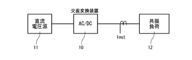
- FIG. 15 shows a circuit configuration of a resonant load power converter (AC / DC converter) connected to the resonant load.
- the AC / DC converter 10 includes a single-phase inverter whose input side is connected to a DC voltage source 11 and whose output side is connected to a resonant load 12 such as an induction heating circuit.
- a rectangular wave voltage is output to the resonant load 12 at the resonant frequency by ON / OFF control of each switching element of the single-phase inverter.
- This AC / DC converter 10 is configured as an induction heating load resonance AC / DC converter (induction heating resonance inverter) when the resonant load 12 is an induction heating circuit.
- alternating current generated by ON / OFF control of each switching element of a single-phase inverter is passed through an LC resonance circuit composed of a coil and a capacitor, and the alternating magnetic field generated thereby is heated.
- An eddy current is applied to a body (electric conductor) and heated from the inside by Joule heat generated thereby.
- an induction heating circuit as a resonant load connected to the output side of a resonant load power converter (for example, the AC / DC converter 10 in FIG. 15) is known to have a property that the current penetration depth decreases as the frequency increases. ing.
- the switching element of the resonance load power converter used for induction heating has an upper limit in the driving frequency, there is a problem that it cannot cope with a voltage frequency higher than the driving frequency of the switching element.
- Patent Document 1 describes that switching control of each switching element of the single-phase inverter of the AC / DC converter 10 of FIG. 15 is performed in a time division manner.
- Patent Documents 2 and 3 have been proposed.
- Patent Document 1 describes a time-sharing operation function of a single-phase inverter in a resonant load power converter, but does not disclose what circuit configuration generates a switching waveform of the single-phase inverter. .
- An object of the present invention is to generate a switching waveform capable of reducing a switching frequency per switching element of a single-phase inverter in a resonant load power conversion device and a resonant load power conversion system including a single-phase inverter. is there.
- the power converter for a resonant load according to claim 1 for solving the above-described problem is a single-phase inverter in which a DC input side is connected to a DC voltage source, an output side is connected to a resonant load, and a rectangular wave voltage is output at a resonant frequency.
- a resonant load power converter comprising: One phase of the single-phase inverter is connected to the upper arm, the lower arm, and the upper and lower arms of the other phase, respectively, and N series bodies of two switching elements (N is an integer of 2 or more) are connected in parallel.
- a switch group circuit configured as follows: A control unit that performs switching control of each switching element of the switch group circuit of the single-phase inverter in a time-sharing manner,
- the controller is A triangular wave generating unit that generates a triangular wave signal having a frequency obtained by dividing the frequency command into a predetermined fraction and having an amplitude value of 0 to 1 and formed by a linear waveform having the same positive and negative inclinations; 4N-1 delay devices for sequentially delaying the triangular wave signal generated by the triangular wave generating unit by 1 / 4N period;
- the reference value set to the value of (2N + 1) / 4N is compared with the triangular wave signal generated by the triangular wave generator and the triangular wave signal delayed by the 4N-1 delay units, and the triangular wave signal is the reference 4N comparators that output a gate ON signal when the value is smaller than the value and a gate OFF signal when the triangular wave signal is larger than the reference value, It is characterized by having.
- a time-sharing operation method for a resonant load power converter wherein a DC input side is connected to a DC voltage source and an output side is connected to a resonant load.
- a time-sharing operation method for a resonant load power conversion device comprising: One phase of the single-phase inverter is connected to the upper arm, the lower arm, and the upper and lower arms of the other phase, respectively, and N series bodies of two switching elements (N is an integer of 2 or more) are connected in parallel.
- a switch group circuit configured as follows: A control unit that performs switching control of each switching element of the switch group circuit of the single-phase inverter in a time-sharing manner,
- the triangular wave generation unit of the control unit has a frequency obtained by dividing a frequency command into a predetermined fraction, and a triangular wave signal formed by a linear waveform having a positive slope and a negative slope having the same slope between amplitude values 0 to 1
- a triangular wave generation step for generating 4N-1 delay units of the control unit sequentially delay the triangular wave signal generated by the triangular wave generation unit by 1 / 4N period;
- a reference value set to a value of (2N + 1) / 4N, a triangular wave signal generated by the triangular wave generation unit, and a triangular wave signal delayed by the 4N-1 delay units. And outputting a gate ON signal when the triangular wave signal is smaller than a reference value, and outputting a gate OFF signal when the triangular wave signal is larger than
- the switching frequency per switching element of a single-phase inverter having 2N switching elements per arm can be lowered.
- a switching pattern capable of time-division operation can be generated regardless of the value N of the parallel number N of the switching element in series.
- the power converter for a resonant load according to claim 2 is the power converter according to claim 1,
- the parallel number N of the serial bodies of the switching elements is 2,
- the switch group circuit of the upper arm of one phase of the single-phase inverter is configured by connecting a series body of switching elements U11 and U12 and a series body of switching elements U21 and U22 in parallel.
- the switch group circuit of the lower arm of one phase of the single-phase inverter is configured by connecting a series body of switching elements X11 and X12 and a series body of switching elements X21 and X22 in parallel.
- the switch group circuit of the upper arm of the other phase of the single-phase inverter is configured by connecting a series body of switching elements V11 and V12 and a series body of switching elements V21 and V22 in parallel.
- the switch group circuit of the lower arm of the other phase of the single-phase inverter is configured by connecting a series body of switching elements Y11 and Y12 and a series body of switching elements Y21 and Y22 in parallel.
- the 4N-1 delay units are configured by first to seventh delay units sequentially provided in series with the triangular wave generation unit, and the 4N comparators include first to eighth comparators.
- the first comparator compares the triangular wave signal generated by the triangular wave generation unit with the reference value, and becomes a gate ON signal for a period of (2N + 1) / 4N of one period of the triangular wave signal, and (2N ⁇ 1) Outputs a gate command signal for the switching elements U11 and Y11, which becomes a gate OFF signal for a period of / 4N
- the second comparator compares the triangular wave signal delayed by the first delay device with the reference value, and delays the gate command signal for U11, Y11 by 1 ⁇ 4 N period, and the gate command signal Output a gate command signal for the switching elements X11 and V11 having the same ON period and OFF period as the ON period and OFF period of
- the third comparator compares the triangular wave signal delayed by the second delay device with the reference value, and delays the gate command signal for X11, V11 by 1 ⁇ 4 N period, and the gate command signal Output a gate command signal for the switching elements U21 and Y21 having the same ON
- the time-sharing operation method of the resonance load power converter according to claim 4 is characterized in that in claim 3,
- the parallel number N of the serial bodies of the switching elements is 2,
- the switch group circuit of the upper arm of one phase of the single-phase inverter is configured by connecting a series body of switching elements U11 and U12 and a series body of switching elements U21 and U22 in parallel.
- the switch group circuit of the lower arm of one phase of the single-phase inverter is configured by connecting a series body of switching elements X11 and X12 and a series body of switching elements X21 and X22 in parallel.
- the switch group circuit of the upper arm of the other phase of the single-phase inverter is configured by connecting a series body of switching elements V11 and V12 and a series body of switching elements V21 and V22 in parallel.
- the switch group circuit of the lower arm of the other phase of the single-phase inverter is configured by connecting a series body of switching elements Y11 and Y12 and a series body of switching elements Y21 and Y22 in parallel.
- the 4N-1 delay units are configured by first to seventh delay units sequentially provided in series with the triangular wave generation unit, and the 4N comparators include first to eighth comparators.
- the first comparator compares the triangular wave signal generated by the triangular wave generator with the reference value, and becomes a gate ON signal for a period of (2N + 1) / 4N of one period of the triangular wave signal, and (2N ⁇ 1) A step of outputting a gate command signal for the switching elements U11 and Y11 that becomes a gate OFF signal for a period of / 4N;
- the second comparator compares the triangular wave signal delayed by the first delay device with the reference value, and delays the gate command signal for U11, Y11 by 1 ⁇ 4N period, and the gate command signal Outputting a gate command signal for switching elements X11 and V11 having the same ON period and OFF period as the ON period and OFF period of
- the third comparator compares the triangular wave signal delayed by the second delay device with the reference value, and delays the gate command signal for X11, V11 by 1 ⁇ 4N period, and the gate command signal Outputting a gate command signal for switching elements U21, Y21 having the same ON period
- the switching frequency per switching element of the single-phase inverter having four switching elements per arm can be lowered.
- the power balance control device in the resonance load power conversion system is: Resonant load power converters equipped with a single-phase inverter that outputs a rectangular wave voltage at the resonant frequency, with the DC input side connected to the DC voltage source and the output side connected to the resonant load side, respectively, in parallel or in series.
- a power balance control device in a power conversion system for a resonant load connected to a resonant load Each of the single-phase inverters of each of the resonance load power converters is connected to one of the upper, lower and upper and lower arms of the single phase inverter, and is connected in series with two switching elements (N is 2).
- switch group circuit configured in parallel, Provided in each of the plurality of resonant load power converters, and performs switching control of each switching element of the switch group circuit of the single-phase inverter in a time-sharing manner while performing power balance control of each resonant load power converter.
- a control unit Each of the control units is Taking a deviation between the average power of the plurality of resonant load power converters and the power of the resonance load power converter to be controlled, a correction amount to be balanced with respect to the average power is obtained and set to the correction amount.
- a balance control unit that adds a current-carrying width command value and outputs a voltage correction value of a single-phase inverter of the resonance load power converter to be controlled;
- a triangular wave generating unit that generates a triangular wave signal having a frequency obtained by dividing the frequency command into a predetermined fraction and having an amplitude value of 0 to 1 and formed by a linear waveform having the same positive and negative inclinations;
- 4N-1 delay devices for sequentially delaying the triangular wave signal generated by the triangular wave generating unit by 1 / 4N period;
- a reference value obtained by subtracting the voltage correction value output from the balance control unit from the value of (2N + 1) / 4N, the triangular wave signal generated by the triangular wave generation unit, and the triangular wave delayed by the 4N-1 delay units 4N comparators that respectively compare the signal and output a gate ON signal when the triangular wave signal is smaller than a reference value, and output a gate OFF signal when the triangular wave
- the power balance control apparatus in the power conversion system for resonant loads according to claim 6 is characterized in that in claim 5,
- the parallel number N of the serial bodies of the switching elements is 2,
- the switch group circuit of the upper arm of one phase of the single-phase inverter is configured by connecting a series body of switching elements U11 and U12 and a series body of switching elements U21 and U22 in parallel.
- the switch group circuit of the lower arm of one phase of the single-phase inverter is configured by connecting a series body of switching elements X11 and X12 and a series body of switching elements X21 and X22 in parallel.
- the switch group circuit of the upper arm of the other phase of the single-phase inverter is configured by connecting a series body of switching elements V11 and V12 and a series body of switching elements V21 and V22 in parallel.
- the switch group circuit of the lower arm of the other phase of the single-phase inverter is configured by connecting a series body of switching elements Y11 and Y12 and a series body of switching elements Y21 and Y22 in parallel.
- the 4N-1 delay units are configured by first to seventh delay units sequentially provided in series with the triangular wave generation unit, and the 4N comparators include first to eighth comparators.
- the first comparator compares the triangular wave signal generated by the triangular wave generation unit with the reference value, and becomes a gate ON signal for a period of (2N + 1) / 4N of one period of the triangular wave signal, and (2N ⁇ 1) Outputs a gate command signal for the switching elements U11 and Y11, which becomes a gate OFF signal for a period of / 4N
- the second comparator compares the triangular wave signal delayed by the first delay device with the reference value, and delays the gate command signal for U11, Y11 by 1 ⁇ 4 N period, and the gate command signal Output a gate command signal for the switching elements X11 and V11 having the same ON period and OFF period as the ON period and OFF period of
- the third comparator compares the triangular wave signal delayed by the second delay device with the reference value, and delays the gate command signal for X11, V11 by 1 ⁇ 4 N period, and the gate command signal Output a gate command signal for the switching elements U21 and Y21 having the same ON
- the power balance control method in the resonance load power conversion system is: Resonant load power converters equipped with a single-phase inverter that outputs a rectangular wave voltage at the resonant frequency, with the DC input side connected to the DC voltage source and the output side connected to the resonant load side, respectively, in parallel or in series.
- a power balance control method for a resonant load power conversion system connected to a resonant load comprising: Each of the single-phase inverters of each of the resonance load power converters is connected to one of the upper, lower and upper and lower arms of the single phase inverter, and is connected in series with two switching elements (N is 2).
- switch group circuit configured in parallel, Provided in each of the plurality of resonant load power converters, and performs switching control of each switching element of the switch group circuit of the single-phase inverter in a time-sharing manner while performing power balance control of each resonant load power converter.
- a control unit The amount of correction that the balance control unit of each control unit takes a deviation between the average power of the plurality of resonant load power converters and the power of the resonance load power converter to be controlled and balances the average power Adding a set energization width command value to the correction amount, and outputting a voltage correction value of the single-phase inverter of the resonance load power converter to be controlled;
- the triangular wave generating unit of each control unit has a frequency obtained by dividing the frequency command into a predetermined fraction, and is a triangular wave formed by a linear waveform having a positive slope and a negative slope having the same slope between amplitude values 0 to 1 Generating a signal; 4N-1 delay units of each control unit sequentially delay the triangular wave signal generated by the triangular wave generation unit by 1 / 4N period; 4N comparators of each control unit include a reference value obtained by subtracting the voltage correction value output from the balance control unit from a value of (2N + 1) / 4N, the tri
- the power balance control method in the power conversion system for a resonant load according to claim 8 is the method of claim 7,
- the parallel number N of the serial bodies of the switching elements is 2,
- the switch group circuit of the upper arm of one phase of the single-phase inverter is configured by connecting a series body of switching elements U11 and U12 and a series body of switching elements U21 and U22 in parallel.
- the switch group circuit of the lower arm of one phase of the single-phase inverter is configured by connecting a series body of switching elements X11 and X12 and a series body of switching elements X21 and X22 in parallel.
- the switch group circuit of the upper arm of the other phase of the single-phase inverter is configured by connecting a series body of switching elements V11 and V12 and a series body of switching elements V21 and V22 in parallel.
- the switch group circuit of the lower arm of the other phase of the single-phase inverter is configured by connecting a series body of switching elements Y11 and Y12 and a series body of switching elements Y21 and Y22 in parallel.
- the 4N-1 delay units are configured by first to seventh delay units sequentially provided in series with the triangular wave generation unit, and the 4N comparators include first to eighth comparators.
- the first comparator compares the triangular wave signal generated by the triangular wave generator with the reference value, and becomes a gate ON signal for a period of (2N + 1) / 4N of one period of the triangular wave signal, and (2N ⁇ 1) A step of outputting a gate command signal for the switching elements U11 and Y11 that becomes a gate OFF signal for a period of / 4N;
- the second comparator compares the triangular wave signal delayed by the first delay device with the reference value, and delays the gate command signal for U11, Y11 by 1 ⁇ 4N period, and the gate command signal Outputting a gate command signal for switching elements X11 and V11 having the same ON period and OFF period as the ON period and OFF period of
- the third comparator compares the triangular wave signal delayed by the second delay device with the reference value, and delays the gate command signal for X11, V11 by 1 ⁇ 4N period, and the gate command signal Outputting a gate command signal for switching elements U21, Y21 having the same ON period
- the switching frequency per switching element of the single-phase inverter having 2N switching elements per arm can be lowered. it can.
- control unit of each resonance load power converter can generate a switching pattern capable of time-division operation regardless of the value N of the parallel number N of the switching elements in series. .
- the switching frequency per switching element of the single-phase inverter having four switching elements per arm can be lowered. it can.
- the switching frequency per switching element of the single-phase inverter having 2N switching elements per arm can be lowered.
- switching that allows time-division operation is possible regardless of the value N of the parallel number N of the switching elements in series. A pattern can be generated.
- the switching frequency per switching element of the single-phase inverter having four switching elements per arm can be lowered.
- Explanatory drawing which shows the on-off period in 1 period of the triangular wave signal in Example 1 of this invention.
- the block diagram of the balance control block by Example 3 of this invention The circuit diagram of the gate signal control block by Example 3 of this invention.
- the circuit diagram of the gate signal control block by Example 4 of this invention The wave form diagram which shows the mode of the gate signal pattern at the time of balance control operation
- FIG. 1 shows a configuration of a single-phase inverter (inverter unit) having a time-sharing operation function applied to, for example, the AC / DC converter 10 of FIG.
- the circuits 100U, 100V, 100X, and 100Y are connected to each other, and a rectangular wave output voltage Vout is output between the common connection point of the switch group circuits 100U and 100X and the common connection point of the switch group circuits 100V and 100Y. It is configured.
- the switch group circuit 100U of the upper arm of one phase of the single-phase inverter has a series body of switching elements U11 and U12, a series body of switching elements U21 and U22, and a series body of switching elements UN1 and UN2 in parallel. It is connected.
- the switch group circuit 100X of the lower arm of one phase of the single-phase inverter includes a series body of switching elements X11 and X12, a series body of switching elements X21 and X22, and a series body of switching elements XN1 and XN2. It is connected.
- the switch group circuit 100V of the upper arm of the other phase of the single-phase inverter includes a series body of switching elements V11 and V12, a series body of switching elements V21 and V22, and a series body of switching elements VN1 and VN2. It is connected.
- the switch group circuit 100Y of the lower arm of the other phase of the single-phase inverter includes a series body of switching elements Y11 and Y12, a series body of switching elements Y21 and Y22, and a series body of switching elements YN1 and YN2. It is connected.
- FIG. 2 shows a control block of a control unit that controls the switching elements of the switch group circuits 100U, 100V, 100X, and 100Y of FIG. 1 in a time-sharing manner.
- reference numeral 111 denotes a frequency divider that divides the frequency of the frequency command signal by 1 / 2N.
- a triangular wave generator 112 generates a triangular wave signal having a frequency divided by the frequency divider 111 and having an amplitude value of 0 to 1 and formed by a linear waveform having the same positive and negative inclinations. It is.
- 114 is a reference value generation unit that generates (sets) a reference value (2N + 1) / 4N for determining an on / off boundary for the triangular wave signal.
- the comparators 115 sequentially shift the triangular wave signal of the triangular wave generation unit 112 that changes the value of (2N + 1) / 4N of the reference value generation unit 114 and the value between 0 and 1, and the 1 Since the comparison is made with a triangular wave signal delayed by / 4N cycles, a gate ON signal becomes a (2N + 1) / 4N period gate ON signal and a (2N-1) / 4N period gate OFF signal of one period of the triangular wave signal. Each command signal is output.
- Each gate command signal output from the 4N comparators 115... Has the same ON period and OFF period, and becomes a gate command signal that is delayed by 1 / 4N period of the triangular wave signal.
- a switching pattern capable of time-division operation can be generated regardless of the value N of the parallel number N of the switching element in series.
- the output voltage period of the single-phase inverter is 1 / 2N of the period T of the triangular wave signal.
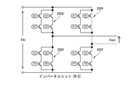
- N 2 of the serial bodies of the switching elements of the switch group circuit of each arm of the single-phase inverter of FIG.
- a series body of switching elements U11 and U12 and a series body of switching elements U21 and U22 are connected in parallel.
- a series body of switching elements X11 and X12 and a series body of switching elements X21 and X22 are connected in parallel.
- a series body of switching elements Y11 and Y12 and a series body of switching elements Y21 and Y22 are connected in parallel.
- the U group (link with the Y group) of the switching elements U11, U12, U21, and U22 generates a positive (upper) voltage as an output voltage
- the switching elements V11, V12, V21, and V22 The V group (link with the X group) generates a negative (lower) voltage as an output voltage.
- FIG. 4 shows a control block of a control unit that performs switching control of the switching elements of the switch group circuits 200U, 200V, 200X, and 200Y of FIG. 3 in a time-sharing manner, and the same parts as those in FIG. .
- 4 differs from FIG. 2 in that 4N ⁇ 1 delay units are configured by first to seventh delay units 113 ⁇ 1 to 113 ⁇ 7 sequentially provided in series with respect to the triangular wave generation unit 112.
- the 4N comparators are configured by first to eighth comparators 115 -1 to 115 -8 , and other parts are configured in the same manner as in FIG.
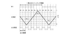
- FIG. 5 shows the relationship between the gate signal pattern and the output voltage by the control block of FIG.
- the middle part of FIG. 5 shows the gate command signals output from the comparators 115 -1 to 115 -8 , respectively, and the lower part of FIG. 5 shows the output voltage.
- the switching frequency per element is 1/4 of the output frequency compared to the frequency of the output voltage (Vout). It will be operated by the signal.
- the interval from time t0 to t8 in FIG. 5 is the operation cycle of one element.
- the switching elements U11 and Y11 are switched on / off simultaneously.
- switching elements U12 and Y12, switching elements U21 and Y21, switching elements U22 and Y22, switching elements V11 and X11, switching elements V12 and X12, switching elements V21 and X21, and switching elements V22 and X22 are simultaneously switched on / off. do.
- each switching element Since the switching frequency of each switching element is 1/4 of the output frequency, there are four times of on (upper side) and four times of off (lower side) in one cycle as shown in the lowermost stage of FIG. . For this reason, it is necessary to perform switching every 1/8 period obtained by dividing one period into eight.
- the gate signal pattern generation process will be described with reference to step 1 to step 7 in FIG.
- the time zone in the gray portion is on.
- Two series (U11 and U12) are turned on at the same time in 8 divisions (1 division is 1/8 period), because there are 2 elements, 2 times, and for equal operation, once in 4 divisions
- the central 3 divisions of the 5 ON divisions of one of the two series elements This is realized by putting an off period of the other element in two series (step 1).
- U on the U2 column is inserted at the center of the off period (3 divisions) of the U1 column (step 2).
- step 3 can be derived from step 1 as a base. That is, the off period of the other element in the two series is inserted into the central three divisions of the five on periods of one element in the two series (U21 and U22).
- step 4 minus is generated in the V1 column with respect to the plus side generated in the U1 column (step 4). It is step 5 that generates this. That is, the off period of the other element in the two series is inserted into the middle three divisions of the five on periods of one element in the two series (V11 and V12). Here, even if the operations of V11 and V12 in step 5 are reversed, the waveform of step 4 generated as a result is the same.
- step 6 a waveform corresponding to the V2 column is generated (step 6). This is generated in step 7 (the operations of step 6 and step 7 are the same as those in step 4 and step 5).
- the gate command signals generated in this way are converted into (1) U11 / Y11, (2) X11 / V11, (3) U21 / Y21, (4) X21 / V21, (7) U12 / Y12, (8) in FIG. ) X12 / V12, (9) U22 / Y22, (10) X22 / V22.
- the signal of the series element may be reversed (the signals of U11 and U12 are reversed). Further, the signals of the parallel elements may be reversed (the signals of the U1 column and the U2 column are reversed).
- the gate command signals (1) U11 / Y11, (2) X11 / V11, (3) U21 / Y21, (4) X21 / V21, (7) U12 / Y12, (8) X12 / V12, (9)
- U22 / Y22 and (10) X22 / V22, (1), (2), (3), (4), (7), (8), (9).
- the triangular wave of (10) is prepared. This is because it is necessary to perform switching every 1/8 cycle as described above.
- the triangular wave is compared with a predetermined reference value, and a value lower than the reference value is turned on, thereby comparing the triangular wave (amplitude value 0 to 1) with 5/8.
- an ON period of 5/8 cycles is obtained.
- That said gate command signal (2) X11 / V11 is the in the comparator 115 -2, were compared delayed triangular wave signal by the delaying unit 113 -1 and (5 upper (2)) the reference value 5/8
- That said gate command signal (3) U21 / Y21 is that in the comparator 115 -3, compared delayed triangular wave signal by the delaying unit 113 -2 and (5 upper (3)) the reference value 5/8
- the gate command signal (2) is delayed by 1/8 cycle with respect to X11 / V11, and the ON period and the OFF period are output as the same signal as the gate command signal (2).
- That said gate command signal (4) X21 / V21 is the in the comparator 115 -4, compared delayed triangular wave signal by the delaying unit 113 -3 and (5 upper (4)) the reference value 5/8
- the gate command signal (3) is delayed by 1/8 cycle with respect to U21 / Y21, and the ON period and the OFF period are output as the same signal as the gate command signal (3).
- the gate command signal (7) U12 / Y12 is in a comparator 115 -5, delay unit 113 delays the triangular wave signal at -4 (5 upper (7)) and the results of comparison of the reference value 5/8
- the gate command signal (4) is delayed by 1/8 cycle with respect to X21 / V21, and the ON period and the OFF period are output as the same signal as the gate command signal (4).
- That said gate command signal (8) X12 / V12 is the in the comparator 115 -6, and compared delayed triangular wave signal by the delaying unit 113 -5 ( Figure 5 upper (8)) and the reference value 5/8
- the gate command signal (7) is delayed by 1/8 cycle with respect to U12 / Y12, and the ON period and the OFF period are output as the same signal as the gate command signal (7).
- That said gate command signal (9) U22 / Y22 is that in the comparator 115 -7 and comparing the reference value 5/8 the delayed triangular wave signal by the delaying unit 113 -6 ( Figure 5 upper (9))
- the gate command signal (8) is delayed by 1/8 cycle with respect to X12 / V12, and the ON period and the OFF period are output as the same signal as the gate command signal (8).
- That said gate command signal (10) X22 / V22 is the in the comparator 115 -8, and compared delayed triangular wave signal by the delaying unit 113 -7 ( Figure 5 upper (10)) and the reference value 5/8
- the gate command signal (9) is delayed by 1/8 cycle with respect to U22 / Y22, and the ON period and the OFF period are output as the same signal as the gate command signal (9).
- the gate command signals (5) and (6) are the gate command signal (5) U31 / Y31 and the gate command signal (6) X31 / Since V31 is used, it is omitted here.
- the positive and negative transitions of the output voltage of the single-phase inverter in FIG. 3 are time t0-t1 plus side (finished when U1 row U12 is off) ⁇ time t1-t2 minus side (V1 row V12 off) End at time t2-t3 plus (end when U2 row U22 is off) ⁇ time t3-t4 minus side (end when V2 row V22 is off) ⁇ time t4-t5 plus side (end when U1 row U11 is off) ⁇ time t5-t6 minus side (end when V1 row V11 is off) ⁇ time t6-t7 plus side (end when U2 row U21 is off) ⁇ time t7-t8 minus side (end when V2 row V21 is off) is there.
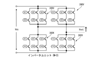
- the switch group circuit 300U of the upper arm of one phase of the single-phase inverter includes a series body of switching elements U11 and U12, a series body of switching elements U21 and U22, and a series body of switching elements U31 and U32. Are connected in parallel.
- the switch group circuit 300X of the lower arm of one phase of the single-phase inverter has a series body of switching elements X11 and X12, a series body of switching elements X21 and X22, and a series body of switching elements X31 and X32 connected in parallel. Has been.
- a series body of switching elements Y11 and Y12, a series body of switching elements Y21 and Y22, and a series body of switching elements Y31 and Y32 are connected in parallel. Has been.
- the control block of the single-phase inverter in FIG. 8 is the same circuit as in FIG. 2, but 4N ⁇ 1 delay elements 113...
- FIG. 2 comprises the first to eleventh delay elements 113...
- the 4N comparators 115 in FIG. 2 comprise the first to twelfth comparators 115. It is. Further, in the dividing period 111, the frequency command signal is divided by 1/6, and the reference value generation unit 114 generates a reference value of 7/12.
- the middle part of FIG. 9 shows gate command signals output from the first comparator (115 -1 ) to the twelfth comparator (115 -12 ), and the lower part of FIG. 9 shows the output voltage. Yes.
- the switching frequency per element is 1/6 of the output frequency compared to the frequency of the output voltage (Vout). It will be operated by the signal.
- the interval from time t0 to t12 in FIG. 9 is the operation cycle of one element.
- the gate signal pattern in the second embodiment has the U3 column in addition to the U column described in FIG. 6, it is basically based on generating ON twice at equal intervals when the U1 column is off. It can be generated by the same process as step 1 to step 7 in FIG.
- the gate command signal (1) U11 / Y11 is generated by the first comparator 115 using the triangular wave signal generated by the triangular wave generator 112 ((1) in the upper part of FIG. 9) and the reference value 7 of the reference value generator 114.
- the gate command signal (2) X11 / V11 is the triangular wave signal ((2) in the upper part of FIG. 9) delayed by the first delay unit 113 and the reference value 7/12.
- the gate command signal (3) U21 / Y21 is obtained by using the triangular wave signal ((3) in the upper stage of FIG. 9) delayed by the second delay device 113 and the reference 7/12.
- the gate command signal (2) X11 / V11 is delayed by 1/12 period, and the ON period and the OFF period are output as the same signal as the gate command signal (2).
- the gate command signal (4) X21 / V21 is the triangular wave signal ((4) in the upper part of FIG. 9) delayed by the third delay device 113 and the reference value 7/12.
- the gate command signal (3) is delayed by 1/12 period with respect to U21 / Y21, and the ON period and the OFF period are output as the same signal as the gate command signal (3).
- the gate command signal (5) U31 / Y31 is the triangular wave signal ((5) in the upper part of FIG. 9) delayed by the fourth delay unit 113 and the reference value 7/12.
- the gate command signal (4) is delayed by 1/12 period with respect to X21 / V21, and the ON period and the OFF period are output as the same signal as the gate command signal (4).
- the gate command signal (6) X31 / V31 is the triangular wave signal ((6) in the upper stage of FIG. 9) delayed by the fifth delay device 113 and the reference value 7/12.
- the gate command signal (5) is delayed by 1/12 period with respect to U31 / Y31, and the ON period and the OFF period are output as the same signal as the gate command signal (5).
- the gate command signal (7) U12 / Y12 is the triangular wave signal ((7) in the upper stage of FIG. 9) delayed by the sixth delay device 113 and the reference value 7/12.
- the gate command signal (6) is delayed by 1/12 period with respect to X31 / V31, and the ON period and the OFF period are output as the same signal as the gate command signal (6).
- the gate command signal (8) X12 / V12 is the triangular wave signal ((8) in the upper part of FIG. 9) delayed by the seventh delay device 113 and the reference value 7/12.
- the gate command signal (7) is delayed by 1/12 period with respect to U12 / Y12, and the ON period and the OFF period are output as the same signal as the gate command signal (7).
- the gate command signal (9) U22 / Y22 is the triangular wave signal ((9) in the upper part of FIG. 9) delayed by the eighth delay device 113 and the reference value 7/12.
- the gate command signal (8) is delayed by 1/12 period with respect to X12 / V12, and the ON period and the OFF period are output as the same signal as the gate command signal (8).
- the gate command signal (10) X22 / V22 is the triangular wave signal ((10) in the upper part of FIG. 9) delayed by the ninth delay device 113 and the reference value 7/12.
- the gate command signal (9) is delayed by 1/12 period with respect to U22 / Y22, and the ON period and the OFF period are output as the same signal as the gate command signal (9).
- the gate command signal (11) U32 / Y32 is the triangular wave signal ((11) in the upper part of FIG. 9) delayed by the tenth delay device 113 and the reference value 7/12.
- the gate command signal (10) X22 / V22 is delayed by 1/12 period, and the ON period and the OFF period are output as the same signal as the gate command signal (10).
- the gate command signal (12) X32 / V32 is the triangular wave signal ((12) in the upper part of FIG. 9) delayed by the eleventh delay device 113 and the reference value 7/12.
- the gate command signal (11) U32 / Y32 is delayed by 1/12 period, and the ON period and the OFF period are output as the same signal as the gate command signal (11).
- the resonant load 12 is connected to the resonant load 12 by connecting a plurality of the AC / DC converters 10 and the DC voltage source 11 on the input side thereof in parallel or in series to form a resonant load power conversion system.
- the output voltage varies depending on the impedance difference between the single-phase inverters, variation in switching timing, and the like.
- a difference occurs in the output voltage phase, and an imbalance occurs in the output power between the inverters.
- a balance control method for a plurality of inverters having a time-sharing operation function has not been proposed conventionally.
- the switching frequency per switching element of the single-phase inverter can be lowered as in the first and second embodiments, and connected in parallel or in series with the resonant load, so that time division operation is performed.
- the power balance control apparatus in the power conversion system for resonance loads which can balance the electric power between the single-phase inverters of the plurality of power conversion apparatuses for resonance load.
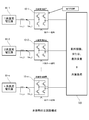
- FIG. 10 shows an overall configuration of a resonant load power conversion system in which a plurality of AC / DC converters (resonant load power converters) including a single-phase inverter are connected in parallel or in series to a resonant load. .
- AC / DC converters resonant load power converters
- the 1-system AC / DC converter 10 -1 includes a single-phase inverter whose input side is connected to the 1-system DC voltage source 11 -1 and whose output side is connected to a resonant load such as an induction heating circuit. .
- the input side is connected to the 2-system to n-system DC voltage sources 11 -2 to 11 -n and the output side is a resonant load.
- a single-phase inverter connected to the
- the AC / DC converters 10 -1 to 10 -n including these single-phase inverters are connected in parallel or series-multiplexed and connected to a resonant load, and are illustrated as a load-side device 120 in FIG.
- an impedance circuit (not shown) is connected between each single-phase inverter and the resonant load.
- the resonant load in the load side device 120 includes, for example, an LC series or parallel resonant circuit.
- Idc -1 to Idc -n indicate DC current detection values obtained by detecting the output currents of the 1-system to n-system DC voltage sources 11 -1 to 11 -n
- Vdc -1 to Vdc -n are The DC voltage detection values obtained by detecting the output voltages of the 1-system to n-system DC voltage sources 11 -1 to 11 -n are shown.
- Each of the AC / DC converters 10 -1 to 10 -n includes the circuit shown in FIG.
- Each single-phase inverter of the AC / DC converters 10 -1 to 10 -n is controlled by a 1-system to n-system gate signal generated based on a balance control command and an energization width command, which will be described later.
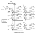
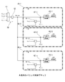
- FIG. 11 shows an example of a balance control block that performs power balance control of the 1-system to n-system AC / DC converters 10 ⁇ 1 to 10 ⁇ n .
- reference numeral 50 denotes an average power calculation circuit
- 60 ⁇ 1 to 60 ⁇ n denote 1-system to n-system power balance control units provided for the AC / DC converters 10 ⁇ 1 to 10 ⁇ n , respectively.
- This is a multiplier that multiplies Idc ⁇ 1 to Idc ⁇ n and outputs each of the 1st to nth system input powers Pdc ⁇ 1 to Pdc ⁇ n .
- Reference numeral 51 of the average power calculation circuit 50 is an adder for summing the 1-system to n-system input powers Pdc -1 to Pdc -n calculated by the multipliers 61 -1 to 61 -n .
- a divider 52 calculates the average input power Pdc -ave by dividing the total input power value of the adder 51 by the number n of AC / DC converters 10 -1 to 10 -n .
- 62 ⁇ 1 to 62 ⁇ n are outputs (averages) from the outputs of multipliers 61 ⁇ 1 to 61 ⁇ n (the 1st to n system input powers Pdc ⁇ 1 to Pdc ⁇ n (detected values)). It is a subtractor that outputs a deviation by subtracting each of input power Pdc -ave (command value)).
- 63 ⁇ 1 to 63 ⁇ n perform a PI operation on the deviation outputs of the subtractors 62 ⁇ 1 to 62 ⁇ n to set a correction amount for balancing the average power (Pdc ⁇ ave ) as a balance control command value.
- Pdc ⁇ ave average power
- the 1-system to n-system power balance control units 60 -1 to 60 -n are set to respective balance control command values obtained by the power balance controllers 63 -1 to 63 -n and are set to energization width command values (not shown). (Energization width ⁇ in FIG. 14 described later) is added, and the voltage correction values of the single-phase inverters of the AC / DC converters 10 -1 to 10 -n are output.
- the voltage correction values obtained by the 1-system to n-system power balance control units 60 -1 to 60 -n are used to generate a reference value to be compared with the triangular wave signal in the gate signal control circuit of FIG. It is done.
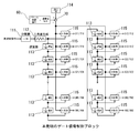
- FIG. 12 shows a gate signal control circuit that is provided corresponding to the 1-system AC / DC converter 10 -1 and controls the switching elements of the switch group circuits 100U, 100V, 100X, and 100Y of FIG. The configuration is shown.
- the circuit of FIG. 12 is also provided corresponding to each of the 2-system to n-system AC / DC converters 10 -2 to 10 -n .
- 111 is a frequency divider that divides the frequency of the frequency command signal by 1 / 2N.
- a triangular wave generator 112 generates a triangular wave signal having a frequency divided by the frequency divider 111 and having an amplitude value of 0 to 1 and formed by a linear waveform having the same positive and negative inclinations. It is.
- 114 is a reference value generation unit that generates (sets) the set value (2N + 1) / 4N.
- the filter 70 deducts the set value of the reference value generator 114 from (2N + 1) / 4N, the output signal of the power balance control unit 60 -1, that is, a voltage correction value (obtained by adding the conducting width command value to balance control command value) It is a subtractor, and the deviation output of the subtractor 70 becomes a reference value for comparison with the triangular wave signal.
- ... is the set value of the reference value generator 114 (2N + 1) / the reference value obtained by subtracting the voltage correction value of the power balance control unit 60 -1 4N, the triangular wave signal and 4N-1 generated by the triangular wave generator 112
- Each of the triangular wave signals sequentially delayed by the delay devices 113 is compared, and when the triangular wave signal is smaller than the reference value, the gate ON signal is obtained, and when the triangular wave signal is larger than the reference value, the gate OFF signal is obtained.
- 4N comparators each outputting a gate command signal of each switching element.
- the comparators 115 Change the reference value, which is the deviation output of the subtractor 70, and the triangular wave signal of the triangular wave generation unit 112 that changes between 0 and 1, and sequentially the 1 / 4N period. Since the triangular wave signal delayed by each is compared, a gate command signal that becomes a gate ON signal for a period of (2N + 1) / 4N of a period of the triangular wave signal and a gate OFF signal for a period of (2N ⁇ 1) / 4N is obtained. Output each.
- the 1-system power balance controller 63 -1 in FIG. controlled in a direction to reduce the voltage correction value outputted from the 1-system power balance control unit 60 -1 obtained by adding the balance control command value energization width command value is small. Therefore, the reference value which is a deviation output of the subtractor 70 in FIG. 12 becomes large in a direction to increase the output power of the AC-DC converter 10 -1 1 system increasing the period of the gate ON signal in one cycle Control.
- the 1-system power balance controller 63 -1 in FIG. 11 controls the direction to increase the balance control command, and the 1 voltage correction value outputted from the power balance control unit 60 -1 of the system increases. Therefore, the reference value which is a deviation output of the subtractor 70 in FIG. 12 becomes smaller in the direction to reduce the output power of the AC-DC converter 10 -1 1 system decreases the period of the gate ON signal in one cycle Control.
- Each gate command signal output from the 4N comparators 115 has the same ON period and OFF period, and becomes a gate command signal delayed by 1 / 4N period of the triangular wave signal.
- the eleven switch group circuits 100U, 100V, 100X, and 100Y are switching-controlled in a time-sharing manner.
- a switching pattern capable of time-division operation can be generated regardless of the value N of the parallel number N of the switching element in series.
- FIG. 13 shows a configuration of a gate signal control circuit that controls switching of the switching group circuits 200U, 200V, 200X, and 200Y of FIG. 3 in a time-sharing manner, and the same parts as those in FIG. Yes.
- the difference from FIG. 12 is that the frequency divider 111 divides the frequency command by 1/4, the reference value generator 114 generates the set value 5/8, and 4N ⁇ 1 delay devices are
- the first to seventh delay devices 113 -1 to 113 -7 are sequentially provided in series with the triangular wave generator 112, and 4N comparators are connected to the first to eighth comparators 115 -1 to 115 -1 .
- 115 located in that configured at -8, other parts are configured in the same manner as FIG.
- FIG. 14 shows the relationship between the gate signal pattern and the output voltage in the circuit of FIG.
- a reference value ie, (5/8) ⁇ (balance control command value + energization width command value)) that is a deviation output of 70 is shown.
- the middle part of FIG. 14 shows the gate command signals output from the comparators 115 -1 to 115 -8, and the lower part of FIG. 14 shows the output voltage.
- the switching frequency per element is 1/4 of the output frequency compared to the frequency of the output voltage (Vout). It will be operated by the signal.
- the interval from time t0 to t8 in FIG. 14 is the operation cycle of one element.
- the switching elements U11 and Y11 are switched on / off simultaneously.
- switching elements U12 and Y12, switching elements U21 and Y21, switching elements U22 and Y22, switching elements V11 and X11, switching elements V12 and X12, switching elements V21 and X21, and switching elements V22 and X22 are simultaneously switched on / off. do.
- each switching element Since the switching frequency of each switching element is 1/4 of the output frequency, there are four times of on (upper side) and four times of off (lower side) in one cycle as shown in the lowermost stage of FIG. . For this reason, it is necessary to perform switching every 1/8 period obtained by dividing one period into eight.
- the middle gate command signals in FIG. 14 (1) U11 / Y11, (2) X11 / V11, (3) U21 / Y21, (4) X21 / V21, (7) U12 / Y12, (8) X12 / V12, ( 9)
- U22 / Y22 and (10) X22 / V22, (1), (2), (3), (4), (7), (8), (9), ( 10)
- the triangular wave is prepared. This is because it is necessary to perform switching every 1/8 cycle as described above.
- a U (Y) group for generating a positive output voltage and a negative output voltage are generated.
- Each switching element of the V (X) group to be switched does not switch from on to off or from off to on at the same time.
- the switching timing has an interval of energization width ⁇ before and after time t1.
- the gate command signal (8) X12 / V12 that generates a negative output voltage is switched from on to off, and the gate command signal (3) U21 / Y21 that generates a positive output voltage is switched off.
- the turn-on timing is spaced by the energization width ⁇ .
- the gate command signal (1) U11 / Y11 is the comparator 115 -1 of Figure 13, compared triangular wave signal generated by the triangular wave generator 112 (FIG. 14 upper (1)) and the output of the subtractor 70 As a result, the signal is output as a signal that turns on the gate for 5/8 of one period of the triangular wave and turns off the gate for 3/8.
- the gate command signal (2) X11 / V11 is in a comparator 115 -2, the delay unit 113 delayed triangular wave signal by -1 (FIG. 14 upper (2)) and the results of comparing the output of the subtractor 70,
- the gate command signal (3) U21 / Y21 is in a comparator 115 -3, delay unit 113 delays the triangular wave signal by 2 (FIG. 14 upper (3)) the result of comparing the output of the subtractor 70,
- the gate command signal (2) is delayed by 1/8 cycle with respect to X11 / V11, and the ON period and the OFF period are output as the same signal as the gate command signal (2).
- the gate command signal (4) X21 / V21 is in a comparator 115 -4, delayer 113 -3 delayed triangular wave signal (FIG. 14 upper (4)) and the results of comparing the output of the subtractor 70,
- the gate command signal (3) is delayed by 1/8 cycle with respect to U21 / Y21, and the ON period and OFF period are output as the same signal as the gate command signal (3).
- the gate command signal (7) U12 / Y12 is in a comparator 115 -5, delayer 113 -4 delayed triangular wave signal (FIG. 14 upper (7)) and the results of comparing the output of the subtractor 70,
- the gate command signal (4) is delayed by 1/8 cycle with respect to X21 / V21, and the ON period and the OFF period are output as the same signal as the gate command signal (4).
- the gate command signals (8) X12 / V12 is in a comparator 115 -6, delayer 113 -5 delayed triangular wave signal (FIG. 14 upper (8)) and the results of comparing the output of the subtractor 70,
- the gate command signal (7) U12 / Y12 is delayed by 1/8 cycle, and the ON period and the OFF period are output as the same signal as the gate command signal (7).
- the gate command signals (9) U22 / Y22 is in a comparator 115 -7, delayer 113 -6 delayed triangular wave signal (FIG. 14 upper (9)) and the results of comparison of the output of the subtractor 70
- the gate command signal (8) is delayed by 1/8 cycle with respect to X12 / V12, and the ON period and the OFF period are output as the same signal as the gate command signal (8).
- the gate command signal (10) X22 / V22 is in a comparator 115 -8, delayed triangular wave signal by the delaying unit 113 -7 (FIG. 14 upper (10)) with the results of comparing the output of the subtractor 70,
- the gate command signal (9) U22 / Y22 is delayed by 1/8 cycle, and the ON period and OFF period are output as the same signal as the gate command signal (9).
- the gate command signals (5) and (6) are omitted here because the gate command signal (5) U31 / Y31 and the gate command signal (6) X31 / V31 in FIG. 9 are used. It is said.
- a plurality of AC / DC converters including a single-phase inverter having four switching elements per arm are connected in parallel or in series to a resonant load.
- the power conversion system for electric power it is possible to balance the power between the plurality of single-phase inverters.
- the switching frequency per switching element of the single-phase inverter having four switching elements per arm can be lowered.
- a switching pattern capable of time-sharing operation can be generated.
Landscapes
- Engineering & Computer Science (AREA)
- Power Engineering (AREA)
- Inverter Devices (AREA)
Abstract
単相インバータの各アームに、2個のスイッチング素子の直列体をN個(Nは2以上の整数)並列に接続して構成されたスイッチ群回路を備えた共振負荷用電力変換装置において、1素子あたりのスイッチング周波数を低減させる。周波数指令の1/2Nの周波数を有し、振幅値0~1の間に、プラスとマイナスが同一傾斜である直線波形により形成された三角波信号を生成する三角波生成部112と、その三角波信号を、1/4N周期ずつ順次遅延させる4N-1個の遅延器113…と、基準値生成部114により(2N+1)/4Nの値に設定した基準値と、前記三角波生成部112で生成された三角波信号および前記4N-1個の遅延器113により遅延された三角波信号とを各々比較し、前記三角波信号が基準値より小のときゲートON信号を、三角波信号が基準値より大のときゲートOFF信号を各々出力する4N個の比較器115…と、を備えた。
Description
本発明は、例えば誘導加熱回路などの共振負荷に矩形波電圧を供給する共振負荷用電力変換装置およびその時分割運転方法と、共振負荷用電力変換システムにおける電力バランス制御装置およびその制御方法に関する。
図15は、共振負荷に接続された共振負荷用電力変換装置(交直変換装置)の回路構成を示している。図15において、交直変換装置10は、入力側が直流電圧源11に接続され、出力側が誘導加熱回路などの共振負荷12に接続された単相インバータを備えている。この単相インバータの各スイッチング素子をON,OFF制御することにより、共振周波数で矩形波電圧を共振負荷12に出力する。
この交直変換装置10は、共振負荷12が誘導加熱回路である場合は、誘導加熱用負荷共振交直変換装置(誘導加熱用共振型インバータ)として構成される。
この誘導加熱用負荷共振交直変換装置は、単相インバータの各スイッチング素子をON、OFF制御して生成した交流を、コイルとキャパシタによるLC共振回路に流し、それによって生成される交番磁界を被加熱体(電気伝導体)に与えて渦電流を流し、これによって発生するジュール熱によって内部から加熱させる方式となっている。
共振負荷用電力変換装置(例えば図15の交直変換装置10)の出力側に接続される共振負荷としての誘導加熱回路は、周波数が高いほど、電流浸透深さが減少する性質が従来から知られている。
例えば電縫管接合(継目を電気抵抗溶接で接合し、管を形成する)においては、表面焼き入れによって行われるため、誘導加熱に用いる共振負荷用電力変換装置には、周波数が高い電圧を出力できることが要求される。
一方で、誘導加熱に用いる共振負荷用電力変換装置のスイッチング素子には、駆動周波数に上限があるため、スイッチング素子の駆動周波数よりも高い電圧周波数に対応ができないことが問題となる。
この問題を解決する先行技術として、例えば特許文献1には、図15の交直変換装置10の単相インバータの各スイッチング素子を時分割でスイッチング制御することが記載されている。また、誘導加熱に関する先行技術文献としては、例えば特許文献2、3に記載のものが提案されている。
特許文献1には、共振負荷用電力変換装置における単相インバータの時分割運転機能は記載されているが、どのような回路構成によって単相インバータのスイッチング波形を生成するかについては開示されていない。
本発明の目的は、単相インバータを備えた共振負荷用電力変換装置、共振負荷用電力変換システムにおいて、単相インバータの1スイッチング素子あたりのスイッチング周波数低減を可能としたスイッチング波形を生成することにある。
上記課題を解決するための請求項1に記載の共振負荷用電力変換装置は、直流入力側が直流電圧源に、出力側が共振負荷に各々接続され、共振周波数で矩形波電圧を出力する単相インバータを備えた共振負荷用電力変換装置であって、
前記単相インバータの一方の相の上、下アームおよび他方の相の上、下アームに各々接続され、2個のスイッチング素子の直列体をN個(Nは2以上の整数)並列に接続して構成されたスイッチ群回路と、
前記単相インバータの前記スイッチ群回路の各スイッチング素子を時分割でスイッチング制御する制御部とを備え、
前記制御部は、
周波数指令を所定分数に分周した周波数を有し、振幅値0~1の間に、プラス傾斜とマイナス傾斜が同一傾斜である直線波形により形成された三角波信号を生成する三角波生成部と、
前記三角波生成部で生成された三角波信号を、1/4N周期ずつ順次遅延させる4N-1個の遅延器と、
(2N+1)/4Nの値に設定した基準値と、前記三角波生成部で生成された三角波信号および前記4N-1個の遅延器により遅延された三角波信号とを各々比較し、前記三角波信号が基準値より小のときゲートON信号を、三角波信号が基準値より大のときゲートOFF信号を各々出力する4N個の比較器と、
を備えていることを特徴とする。
前記単相インバータの一方の相の上、下アームおよび他方の相の上、下アームに各々接続され、2個のスイッチング素子の直列体をN個(Nは2以上の整数)並列に接続して構成されたスイッチ群回路と、
前記単相インバータの前記スイッチ群回路の各スイッチング素子を時分割でスイッチング制御する制御部とを備え、
前記制御部は、
周波数指令を所定分数に分周した周波数を有し、振幅値0~1の間に、プラス傾斜とマイナス傾斜が同一傾斜である直線波形により形成された三角波信号を生成する三角波生成部と、
前記三角波生成部で生成された三角波信号を、1/4N周期ずつ順次遅延させる4N-1個の遅延器と、
(2N+1)/4Nの値に設定した基準値と、前記三角波生成部で生成された三角波信号および前記4N-1個の遅延器により遅延された三角波信号とを各々比較し、前記三角波信号が基準値より小のときゲートON信号を、三角波信号が基準値より大のときゲートOFF信号を各々出力する4N個の比較器と、
を備えていることを特徴とする。
また、請求項3に記載の共振負荷用電力変換装置の時分割運転方法は、直流入力側が直流電圧源に、出力側が共振負荷に各々接続され、共振周波数で矩形波電圧を出力する単相インバータを備えた共振負荷用電力変換装置の時分割運転方法であって、
前記単相インバータの一方の相の上、下アームおよび他方の相の上、下アームに各々接続され、2個のスイッチング素子の直列体をN個(Nは2以上の整数)並列に接続して構成されたスイッチ群回路と、
前記単相インバータの前記スイッチ群回路の各スイッチング素子を時分割でスイッチング制御する制御部とを備え、
前記制御部の三角波生成部が、周波数指令を所定分数に分周した周波数を有し、振幅値0~1の間に、プラス傾斜とマイナス傾斜が同一傾斜である直線波形により形成された三角波信号を生成する三角波生成ステップと、
前記制御部の4N-1個の遅延器が、前記三角波生成部で生成された三角波信号を、1/4N周期ずつ順次遅延させるステップと、
前記制御部の4N個の比較器が、(2N+1)/4Nの値に設定した基準値と、前記三角波生成部で生成された三角波信号および前記4N-1個の遅延器により遅延された三角波信号とを各々比較し、前記三角波信号が基準値より小のときゲートON信号を、三角波信号が基準値より大のときゲートOFF信号を各々出力するステップと、
を備えていることを特徴とする。
前記単相インバータの一方の相の上、下アームおよび他方の相の上、下アームに各々接続され、2個のスイッチング素子の直列体をN個(Nは2以上の整数)並列に接続して構成されたスイッチ群回路と、
前記単相インバータの前記スイッチ群回路の各スイッチング素子を時分割でスイッチング制御する制御部とを備え、
前記制御部の三角波生成部が、周波数指令を所定分数に分周した周波数を有し、振幅値0~1の間に、プラス傾斜とマイナス傾斜が同一傾斜である直線波形により形成された三角波信号を生成する三角波生成ステップと、
前記制御部の4N-1個の遅延器が、前記三角波生成部で生成された三角波信号を、1/4N周期ずつ順次遅延させるステップと、
前記制御部の4N個の比較器が、(2N+1)/4Nの値に設定した基準値と、前記三角波生成部で生成された三角波信号および前記4N-1個の遅延器により遅延された三角波信号とを各々比較し、前記三角波信号が基準値より小のときゲートON信号を、三角波信号が基準値より大のときゲートOFF信号を各々出力するステップと、
を備えていることを特徴とする。
上記構成によれば、1アーム毎に2N個のスイッチング素子を有した単相インバータの、1スイッチング素子あたりのスイッチング周波数を下げることができる。
また、スイッチング素子の直列体の並列数Nが、2以上のどのような値であっても、時分割運転が可能なスイッチングパターンを生成することができる。
また、請求項2に記載の共振負荷用電力変換装置は、請求項1において、
前記スイッチング素子の直列体の並列個数Nは2であり、
前記単相インバータの一方の相の上アームのスイッチ群回路は、スイッチング素子U11,U12の直列体とスイッチング素子U21,U22の直列体とを並列に接続して構成され、
前記単相インバータの一方の相の下アームのスイッチ群回路は、スイッチング素子X11,X12の直列体とスイッチング素子X21,X22の直列体とを並列に接続して構成され、
前記単相インバータの他方の相の上アームのスイッチ群回路は、スイッチング素子V11,V12の直列体とスイッチング素子V21,V22の直列体とを並列に接続して構成され、
前記単相インバータの他方の相の下アームのスイッチ群回路は、スイッチング素子Y11,Y12の直列体とスイッチング素子Y21,Y22の直列体とを並列に接続して構成され、
前記4N-1個の遅延器は、前記三角波生成部に対して順次直列に設けた第1~第7の遅延器で構成され、前記4N個の比較器は、第1~第8の比較器で構成され、
前記第1の比較器は、前記三角波生成部で生成された三角波信号と前記基準値を比較し、前記三角波信号の1周期の(2N+1)/4Nの期間ゲートON信号となり、(2N-1)/4Nの期間ゲートOFF信号となるスイッチング素子U11、Y11用ゲート指令信号を出力し、
前記第2の比較器は、前記第1の遅延器により遅延された三角波信号と前記基準値を比較し、前記U11、Y11用ゲート指令信号に対して1/4N周期遅延し、当該ゲート指令信号のON期間およびOFF期間と同一のON期間およびOFF期間を有するスイッチング素子X11、V11用ゲート指令信号を出力し、
前記第3の比較器は、前記第2の遅延器により遅延された三角波信号と前記基準値を比較し、前記X11、V11用ゲート指令信号に対して1/4N周期遅延し、当該ゲート指令信号のON期間およびOFF期間と同一のON期間およびOFF期間を有するスイッチング素子U21、Y21用ゲート指令信号を出力し、
前記第4の比較器は、前記第3の遅延器により遅延された三角波信号と前記基準値を比較し、前記U21、Y21用ゲート指令信号に対して1/4N周期遅延し、当該ゲート指令信号のON期間およびOFF期間と同一のON期間およびOFF期間を有するスイッチング素子X21、V21用ゲート指令信号を出力し、
前記第5の比較器は、前記第4の遅延器により遅延された三角波信号と前記基準値を比較し、前記X21、V21用ゲート指令信号に対して1/4N周期遅延し、当該ゲート指令信号のON期間およびOFF期間と同一のON期間およびOFF期間を有するスイッチング素子U12、Y12用ゲート指令信号を出力し、
前記第6の比較器は、前記第5の遅延器により遅延された三角波信号と前記基準値を比較し、前記U12、Y12用ゲート指令信号に対して1/4N周期遅延し、当該ゲート指令信号のON期間およびOFF期間と同一のON期間およびOFF期間を有するスイッチング素子X12、V12用ゲート指令信号を出力し、
前記第7の比較器は、前記第6の遅延器により遅延された三角波信号と前記基準値を比較し、前記X12、V12用ゲート指令信号に対して1/4N周期遅延し、当該ゲート指令信号のON期間およびOFF期間と同一のON期間およびOFF期間を有するスイッチング素子U22、Y22用ゲート指令信号を出力し、
前記第8の比較器は、前記第7の遅延器により遅延された三角波信号と前記基準値を比較し、前記U22、Y22用ゲート指令信号に対して1/4N周期遅延し、当該ゲート指令信号のON期間およびOFF期間と同一のON期間およびOFF期間を有するスイッチング素子X22、V22用ゲート指令信号を出力することを特徴とする。
前記スイッチング素子の直列体の並列個数Nは2であり、
前記単相インバータの一方の相の上アームのスイッチ群回路は、スイッチング素子U11,U12の直列体とスイッチング素子U21,U22の直列体とを並列に接続して構成され、
前記単相インバータの一方の相の下アームのスイッチ群回路は、スイッチング素子X11,X12の直列体とスイッチング素子X21,X22の直列体とを並列に接続して構成され、
前記単相インバータの他方の相の上アームのスイッチ群回路は、スイッチング素子V11,V12の直列体とスイッチング素子V21,V22の直列体とを並列に接続して構成され、
前記単相インバータの他方の相の下アームのスイッチ群回路は、スイッチング素子Y11,Y12の直列体とスイッチング素子Y21,Y22の直列体とを並列に接続して構成され、
前記4N-1個の遅延器は、前記三角波生成部に対して順次直列に設けた第1~第7の遅延器で構成され、前記4N個の比較器は、第1~第8の比較器で構成され、
前記第1の比較器は、前記三角波生成部で生成された三角波信号と前記基準値を比較し、前記三角波信号の1周期の(2N+1)/4Nの期間ゲートON信号となり、(2N-1)/4Nの期間ゲートOFF信号となるスイッチング素子U11、Y11用ゲート指令信号を出力し、
前記第2の比較器は、前記第1の遅延器により遅延された三角波信号と前記基準値を比較し、前記U11、Y11用ゲート指令信号に対して1/4N周期遅延し、当該ゲート指令信号のON期間およびOFF期間と同一のON期間およびOFF期間を有するスイッチング素子X11、V11用ゲート指令信号を出力し、
前記第3の比較器は、前記第2の遅延器により遅延された三角波信号と前記基準値を比較し、前記X11、V11用ゲート指令信号に対して1/4N周期遅延し、当該ゲート指令信号のON期間およびOFF期間と同一のON期間およびOFF期間を有するスイッチング素子U21、Y21用ゲート指令信号を出力し、
前記第4の比較器は、前記第3の遅延器により遅延された三角波信号と前記基準値を比較し、前記U21、Y21用ゲート指令信号に対して1/4N周期遅延し、当該ゲート指令信号のON期間およびOFF期間と同一のON期間およびOFF期間を有するスイッチング素子X21、V21用ゲート指令信号を出力し、
前記第5の比較器は、前記第4の遅延器により遅延された三角波信号と前記基準値を比較し、前記X21、V21用ゲート指令信号に対して1/4N周期遅延し、当該ゲート指令信号のON期間およびOFF期間と同一のON期間およびOFF期間を有するスイッチング素子U12、Y12用ゲート指令信号を出力し、
前記第6の比較器は、前記第5の遅延器により遅延された三角波信号と前記基準値を比較し、前記U12、Y12用ゲート指令信号に対して1/4N周期遅延し、当該ゲート指令信号のON期間およびOFF期間と同一のON期間およびOFF期間を有するスイッチング素子X12、V12用ゲート指令信号を出力し、
前記第7の比較器は、前記第6の遅延器により遅延された三角波信号と前記基準値を比較し、前記X12、V12用ゲート指令信号に対して1/4N周期遅延し、当該ゲート指令信号のON期間およびOFF期間と同一のON期間およびOFF期間を有するスイッチング素子U22、Y22用ゲート指令信号を出力し、
前記第8の比較器は、前記第7の遅延器により遅延された三角波信号と前記基準値を比較し、前記U22、Y22用ゲート指令信号に対して1/4N周期遅延し、当該ゲート指令信号のON期間およびOFF期間と同一のON期間およびOFF期間を有するスイッチング素子X22、V22用ゲート指令信号を出力することを特徴とする。
また、請求項4に記載の共振負荷用電力変換装置の時分割運転方法は、請求項3において、
前記スイッチング素子の直列体の並列個数Nは2であり、
前記単相インバータの一方の相の上アームのスイッチ群回路は、スイッチング素子U11,U12の直列体とスイッチング素子U21,U22の直列体とを並列に接続して構成され、
前記単相インバータの一方の相の下アームのスイッチ群回路は、スイッチング素子X11,X12の直列体とスイッチング素子X21,X22の直列体とを並列に接続して構成され、
前記単相インバータの他方の相の上アームのスイッチ群回路は、スイッチング素子V11,V12の直列体とスイッチング素子V21,V22の直列体とを並列に接続して構成され、
前記単相インバータの他方の相の下アームのスイッチ群回路は、スイッチング素子Y11,Y12の直列体とスイッチング素子Y21,Y22の直列体とを並列に接続して構成され、
前記4N-1個の遅延器は、前記三角波生成部に対して順次直列に設けた第1~第7の遅延器で構成され、前記4N個の比較器は、第1~第8の比較器で構成され、
前記第1の比較器が、前記三角波生成部で生成された三角波信号と前記基準値を比較し、前記三角波信号の1周期の(2N+1)/4Nの期間ゲートON信号となり、(2N-1)/4Nの期間ゲートOFF信号となるスイッチング素子U11、Y11用ゲート指令信号を出力するステップと、
前記第2の比較器が、前記第1の遅延器により遅延された三角波信号と前記基準値を比較し、前記U11、Y11用ゲート指令信号に対して1/4N周期遅延し、当該ゲート指令信号のON期間およびOFF期間と同一のON期間およびOFF期間を有するスイッチング素子X11、V11用ゲート指令信号を出力するステップと、
前記第3の比較器が、前記第2の遅延器により遅延された三角波信号と前記基準値を比較し、前記X11、V11用ゲート指令信号に対して1/4N周期遅延し、当該ゲート指令信号のON期間およびOFF期間と同一のON期間およびOFF期間を有するスイッチング素子U21、Y21用ゲート指令信号を出力するステップと、
前記第4の比較器が、前記第3の遅延器により遅延された三角波信号と前記基準値を比較し、前記U21、Y21用ゲート指令信号に対して1/4N周期遅延し、当該ゲート指令信号のON期間およびOFF期間と同一のON期間およびOFF期間を有するスイッチング素子X21、V21用ゲート指令信号を出力するステップと、
前記第5の比較器が、前記第4の遅延器により遅延された三角波信号と前記基準値を比較し、前記X21、V21用ゲート指令信号に対して1/4N周期遅延し、当該ゲート指令信号のON期間およびOFF期間と同一のON期間およびOFF期間を有するスイッチング素子U12、Y12用ゲート指令信号を出力するステップと、
前記第6の比較器が、前記第5の遅延器により遅延された三角波信号と前記基準値を比較し、前記U12、Y12用ゲート指令信号に対して1/4N周期遅延し、当該ゲート指令信号のON期間およびOFF期間と同一のON期間およびOFF期間を有するスイッチング素子X12、V12用ゲート指令信号を出力するステップと、
前記第7の比較器が、前記第6の遅延器により遅延された三角波信号と前記基準値を比較し、前記X12、V12用ゲート指令信号に対して1/4N周期遅延し、当該ゲート指令信号のON期間およびOFF期間と同一のON期間およびOFF期間を有するスイッチング素子U22、Y22用ゲート指令信号を出力するステップと、
前記第8の比較器が、前記第7の遅延器により遅延された三角波信号と前記基準値を比較し、前記U22、Y22用ゲート指令信号に対して1/4N周期遅延し、当該ゲート指令信号のON期間およびOFF期間と同一のON期間およびOFF期間を有するスイッチング素子X22、V22用ゲート指令信号を出力するステップと、
を備えたことを特徴とする。
前記スイッチング素子の直列体の並列個数Nは2であり、
前記単相インバータの一方の相の上アームのスイッチ群回路は、スイッチング素子U11,U12の直列体とスイッチング素子U21,U22の直列体とを並列に接続して構成され、
前記単相インバータの一方の相の下アームのスイッチ群回路は、スイッチング素子X11,X12の直列体とスイッチング素子X21,X22の直列体とを並列に接続して構成され、
前記単相インバータの他方の相の上アームのスイッチ群回路は、スイッチング素子V11,V12の直列体とスイッチング素子V21,V22の直列体とを並列に接続して構成され、
前記単相インバータの他方の相の下アームのスイッチ群回路は、スイッチング素子Y11,Y12の直列体とスイッチング素子Y21,Y22の直列体とを並列に接続して構成され、
前記4N-1個の遅延器は、前記三角波生成部に対して順次直列に設けた第1~第7の遅延器で構成され、前記4N個の比較器は、第1~第8の比較器で構成され、
前記第1の比較器が、前記三角波生成部で生成された三角波信号と前記基準値を比較し、前記三角波信号の1周期の(2N+1)/4Nの期間ゲートON信号となり、(2N-1)/4Nの期間ゲートOFF信号となるスイッチング素子U11、Y11用ゲート指令信号を出力するステップと、
前記第2の比較器が、前記第1の遅延器により遅延された三角波信号と前記基準値を比較し、前記U11、Y11用ゲート指令信号に対して1/4N周期遅延し、当該ゲート指令信号のON期間およびOFF期間と同一のON期間およびOFF期間を有するスイッチング素子X11、V11用ゲート指令信号を出力するステップと、
前記第3の比較器が、前記第2の遅延器により遅延された三角波信号と前記基準値を比較し、前記X11、V11用ゲート指令信号に対して1/4N周期遅延し、当該ゲート指令信号のON期間およびOFF期間と同一のON期間およびOFF期間を有するスイッチング素子U21、Y21用ゲート指令信号を出力するステップと、
前記第4の比較器が、前記第3の遅延器により遅延された三角波信号と前記基準値を比較し、前記U21、Y21用ゲート指令信号に対して1/4N周期遅延し、当該ゲート指令信号のON期間およびOFF期間と同一のON期間およびOFF期間を有するスイッチング素子X21、V21用ゲート指令信号を出力するステップと、
前記第5の比較器が、前記第4の遅延器により遅延された三角波信号と前記基準値を比較し、前記X21、V21用ゲート指令信号に対して1/4N周期遅延し、当該ゲート指令信号のON期間およびOFF期間と同一のON期間およびOFF期間を有するスイッチング素子U12、Y12用ゲート指令信号を出力するステップと、
前記第6の比較器が、前記第5の遅延器により遅延された三角波信号と前記基準値を比較し、前記U12、Y12用ゲート指令信号に対して1/4N周期遅延し、当該ゲート指令信号のON期間およびOFF期間と同一のON期間およびOFF期間を有するスイッチング素子X12、V12用ゲート指令信号を出力するステップと、
前記第7の比較器が、前記第6の遅延器により遅延された三角波信号と前記基準値を比較し、前記X12、V12用ゲート指令信号に対して1/4N周期遅延し、当該ゲート指令信号のON期間およびOFF期間と同一のON期間およびOFF期間を有するスイッチング素子U22、Y22用ゲート指令信号を出力するステップと、
前記第8の比較器が、前記第7の遅延器により遅延された三角波信号と前記基準値を比較し、前記U22、Y22用ゲート指令信号に対して1/4N周期遅延し、当該ゲート指令信号のON期間およびOFF期間と同一のON期間およびOFF期間を有するスイッチング素子X22、V22用ゲート指令信号を出力するステップと、
を備えたことを特徴とする。
上記構成によれば、1アーム毎に4個のスイッチング素子を有した単相インバータの、1スイッチング素子あたりのスイッチング周波数を下げることができる。
また、請求項5に記載の共振負荷用電力変換システムにおける電力バランス制御装置は、
直流入力側が直流電圧源に、出力側が共振負荷側に各々接続され、共振周波数で矩形波電圧を出力する単相インバータを備えた共振負荷用電力変換装置を、複数並列に、又は直列多重化して共振負荷に接続した共振負荷用電力変換システムにおける電力バランス制御装置であって、
前記各共振負荷用電力変換装置の単相インバータの一方の相の上、下アームおよび他方の相の上、下アームに各々接続され、2個のスイッチング素子の直列体をN個(Nは2以上の整数)並列に接続して構成されたスイッチ群回路と、
前記複数の共振負荷用電力変換装置各々に設けられ、各共振負荷用電力変換装置の電力のバランス制御を行いつつ、前記単相インバータの前記スイッチ群回路の各スイッチング素子を時分割でスイッチング制御する制御部とを備え、
前記各制御部は、
前記複数の共振負荷用電力変換装置の平均電力と制御対象の共振負荷用電力変換装置の電力との偏差をとって、平均電力に対してバランスさせる補正量を求め、該補正量に、設定した通電幅指令値を加算して、当該制御対象の共振負荷用電力変換装置の単相インバータの電圧補正値を出力するバランス制御部と、
周波数指令を所定分数に分周した周波数を有し、振幅値0~1の間に、プラス傾斜とマイナス傾斜が同一傾斜である直線波形により形成された三角波信号を生成する三角波生成部と、
前記三角波生成部で生成された三角波信号を、1/4N周期ずつ順次遅延させる4N-1個の遅延器と、
(2N+1)/4Nの値から前記バランス制御部で出力された電圧補正値を差し引いた基準値と、前記三角波生成部で生成された三角波信号および前記4N-1個の遅延器により遅延された三角波信号とを各々比較し、前記三角波信号が基準値より小のときゲートON信号を、三角波信号が基準値より大のときゲートOFF信号を各々出力する4N個の比較器と、
を各々備えていることを特徴とする。
直流入力側が直流電圧源に、出力側が共振負荷側に各々接続され、共振周波数で矩形波電圧を出力する単相インバータを備えた共振負荷用電力変換装置を、複数並列に、又は直列多重化して共振負荷に接続した共振負荷用電力変換システムにおける電力バランス制御装置であって、
前記各共振負荷用電力変換装置の単相インバータの一方の相の上、下アームおよび他方の相の上、下アームに各々接続され、2個のスイッチング素子の直列体をN個(Nは2以上の整数)並列に接続して構成されたスイッチ群回路と、
前記複数の共振負荷用電力変換装置各々に設けられ、各共振負荷用電力変換装置の電力のバランス制御を行いつつ、前記単相インバータの前記スイッチ群回路の各スイッチング素子を時分割でスイッチング制御する制御部とを備え、
前記各制御部は、
前記複数の共振負荷用電力変換装置の平均電力と制御対象の共振負荷用電力変換装置の電力との偏差をとって、平均電力に対してバランスさせる補正量を求め、該補正量に、設定した通電幅指令値を加算して、当該制御対象の共振負荷用電力変換装置の単相インバータの電圧補正値を出力するバランス制御部と、
周波数指令を所定分数に分周した周波数を有し、振幅値0~1の間に、プラス傾斜とマイナス傾斜が同一傾斜である直線波形により形成された三角波信号を生成する三角波生成部と、
前記三角波生成部で生成された三角波信号を、1/4N周期ずつ順次遅延させる4N-1個の遅延器と、
(2N+1)/4Nの値から前記バランス制御部で出力された電圧補正値を差し引いた基準値と、前記三角波生成部で生成された三角波信号および前記4N-1個の遅延器により遅延された三角波信号とを各々比較し、前記三角波信号が基準値より小のときゲートON信号を、三角波信号が基準値より大のときゲートOFF信号を各々出力する4N個の比較器と、
を各々備えていることを特徴とする。
また、請求項6に記載の共振負荷用電力変換システムにおける電力バランス制御装置は、請求項5において、
前記スイッチング素子の直列体の並列個数Nは2であり、
前記単相インバータの一方の相の上アームのスイッチ群回路は、スイッチング素子U11,U12の直列体とスイッチング素子U21,U22の直列体とを並列に接続して構成され、
前記単相インバータの一方の相の下アームのスイッチ群回路は、スイッチング素子X11,X12の直列体とスイッチング素子X21,X22の直列体とを並列に接続して構成され、
前記単相インバータの他方の相の上アームのスイッチ群回路は、スイッチング素子V11,V12の直列体とスイッチング素子V21,V22の直列体とを並列に接続して構成され、
前記単相インバータの他方の相の下アームのスイッチ群回路は、スイッチング素子Y11,Y12の直列体とスイッチング素子Y21,Y22の直列体とを並列に接続して構成され、
前記4N-1個の遅延器は、前記三角波生成部に対して順次直列に設けた第1~第7の遅延器で構成され、前記4N個の比較器は、第1~第8の比較器で構成され、
前記第1の比較器は、前記三角波生成部で生成された三角波信号と前記基準値を比較し、前記三角波信号の1周期の(2N+1)/4Nの期間ゲートON信号となり、(2N-1)/4Nの期間ゲートOFF信号となるスイッチング素子U11、Y11用ゲート指令信号を出力し、
前記第2の比較器は、前記第1の遅延器により遅延された三角波信号と前記基準値を比較し、前記U11、Y11用ゲート指令信号に対して1/4N周期遅延し、当該ゲート指令信号のON期間およびOFF期間と同一のON期間およびOFF期間を有するスイッチング素子X11、V11用ゲート指令信号を出力し、
前記第3の比較器は、前記第2の遅延器により遅延された三角波信号と前記基準値を比較し、前記X11、V11用ゲート指令信号に対して1/4N周期遅延し、当該ゲート指令信号のON期間およびOFF期間と同一のON期間およびOFF期間を有するスイッチング素子U21、Y21用ゲート指令信号を出力し、
前記第4の比較器は、前記第3の遅延器により遅延された三角波信号と前記基準値を比較し、前記U21、Y21用ゲート指令信号に対して1/4N周期遅延し、当該ゲート指令信号のON期間およびOFF期間と同一のON期間およびOFF期間を有するスイッチング素子X21、V21用ゲート指令信号を出力し、
前記第5の比較器は、前記第4の遅延器により遅延された三角波信号と前記基準値を比較し、前記X21、V21用ゲート指令信号に対して1/4N周期遅延し、当該ゲート指令信号のON期間およびOFF期間と同一のON期間およびOFF期間を有するスイッチング素子U12、Y12用ゲート指令信号を出力し、
前記第6の比較器は、前記第5の遅延器により遅延された三角波信号と前記基準値を比較し、前記U12、Y12用ゲート指令信号に対して1/4N周期遅延し、当該ゲート指令信号のON期間およびOFF期間と同一のON期間およびOFF期間を有するスイッチング素子X12、V12用ゲート指令信号を出力し、
前記第7の比較器は、前記第6の遅延器により遅延された三角波信号と前記基準値を比較し、前記X12、V12用ゲート指令信号に対して1/4N周期遅延し、当該ゲート指令信号のON期間およびOFF期間と同一のON期間およびOFF期間を有するスイッチング素子U22、Y22用ゲート指令信号を出力し、
前記第8の比較器は、前記第7の遅延器により遅延された三角波信号と前記基準値を比較し、前記U22、Y22用ゲート指令信号に対して1/4N周期遅延し、当該ゲート指令信号のON期間およびOFF期間と同一のON期間およびOFF期間を有するスイッチング素子X22、V22用ゲート指令信号を出力することを特徴としている。
前記スイッチング素子の直列体の並列個数Nは2であり、
前記単相インバータの一方の相の上アームのスイッチ群回路は、スイッチング素子U11,U12の直列体とスイッチング素子U21,U22の直列体とを並列に接続して構成され、
前記単相インバータの一方の相の下アームのスイッチ群回路は、スイッチング素子X11,X12の直列体とスイッチング素子X21,X22の直列体とを並列に接続して構成され、
前記単相インバータの他方の相の上アームのスイッチ群回路は、スイッチング素子V11,V12の直列体とスイッチング素子V21,V22の直列体とを並列に接続して構成され、
前記単相インバータの他方の相の下アームのスイッチ群回路は、スイッチング素子Y11,Y12の直列体とスイッチング素子Y21,Y22の直列体とを並列に接続して構成され、
前記4N-1個の遅延器は、前記三角波生成部に対して順次直列に設けた第1~第7の遅延器で構成され、前記4N個の比較器は、第1~第8の比較器で構成され、
前記第1の比較器は、前記三角波生成部で生成された三角波信号と前記基準値を比較し、前記三角波信号の1周期の(2N+1)/4Nの期間ゲートON信号となり、(2N-1)/4Nの期間ゲートOFF信号となるスイッチング素子U11、Y11用ゲート指令信号を出力し、
前記第2の比較器は、前記第1の遅延器により遅延された三角波信号と前記基準値を比較し、前記U11、Y11用ゲート指令信号に対して1/4N周期遅延し、当該ゲート指令信号のON期間およびOFF期間と同一のON期間およびOFF期間を有するスイッチング素子X11、V11用ゲート指令信号を出力し、
前記第3の比較器は、前記第2の遅延器により遅延された三角波信号と前記基準値を比較し、前記X11、V11用ゲート指令信号に対して1/4N周期遅延し、当該ゲート指令信号のON期間およびOFF期間と同一のON期間およびOFF期間を有するスイッチング素子U21、Y21用ゲート指令信号を出力し、
前記第4の比較器は、前記第3の遅延器により遅延された三角波信号と前記基準値を比較し、前記U21、Y21用ゲート指令信号に対して1/4N周期遅延し、当該ゲート指令信号のON期間およびOFF期間と同一のON期間およびOFF期間を有するスイッチング素子X21、V21用ゲート指令信号を出力し、
前記第5の比較器は、前記第4の遅延器により遅延された三角波信号と前記基準値を比較し、前記X21、V21用ゲート指令信号に対して1/4N周期遅延し、当該ゲート指令信号のON期間およびOFF期間と同一のON期間およびOFF期間を有するスイッチング素子U12、Y12用ゲート指令信号を出力し、
前記第6の比較器は、前記第5の遅延器により遅延された三角波信号と前記基準値を比較し、前記U12、Y12用ゲート指令信号に対して1/4N周期遅延し、当該ゲート指令信号のON期間およびOFF期間と同一のON期間およびOFF期間を有するスイッチング素子X12、V12用ゲート指令信号を出力し、
前記第7の比較器は、前記第6の遅延器により遅延された三角波信号と前記基準値を比較し、前記X12、V12用ゲート指令信号に対して1/4N周期遅延し、当該ゲート指令信号のON期間およびOFF期間と同一のON期間およびOFF期間を有するスイッチング素子U22、Y22用ゲート指令信号を出力し、
前記第8の比較器は、前記第7の遅延器により遅延された三角波信号と前記基準値を比較し、前記U22、Y22用ゲート指令信号に対して1/4N周期遅延し、当該ゲート指令信号のON期間およびOFF期間と同一のON期間およびOFF期間を有するスイッチング素子X22、V22用ゲート指令信号を出力することを特徴としている。
また、請求項7に記載の共振負荷用電力変換システムにおける電力バランス制御方法は、
直流入力側が直流電圧源に、出力側が共振負荷側に各々接続され、共振周波数で矩形波電圧を出力する単相インバータを備えた共振負荷用電力変換装置を、複数並列に、又は直列多重化して共振負荷に接続した共振負荷用電力変換システムにおける電力バランス制御方法であって、
前記各共振負荷用電力変換装置の単相インバータの一方の相の上、下アームおよび他方の相の上、下アームに各々接続され、2個のスイッチング素子の直列体をN個(Nは2以上の整数)並列に接続して構成されたスイッチ群回路と、
前記複数の共振負荷用電力変換装置各々に設けられ、各共振負荷用電力変換装置の電力のバランス制御を行いつつ、前記単相インバータの前記スイッチ群回路の各スイッチング素子を時分割でスイッチング制御する制御部とを備え、
前記各制御部のバランス制御部が、前記複数の共振負荷用電力変換装置の平均電力と制御対象の共振負荷用電力変換装置の電力との偏差をとって、平均電力に対してバランスさせる補正量を求め、該補正量に、設定した通電幅指令値を加算して、当該制御対象の共振負荷用電力変換装置の単相インバータの電圧補正値を出力するステップと、
前記各制御部の三角波生成部が、周波数指令を所定分数に分周した周波数を有し、振幅値0~1の間に、プラス傾斜とマイナス傾斜が同一傾斜である直線波形により形成された三角波信号を生成するステップと、
前記各制御部の4N-1個の遅延器が、前記三角波生成部で生成された三角波信号を、1/4N周期ずつ順次遅延させるステップと、
前記各制御部の4N個の比較器が、(2N+1)/4Nの値から前記バランス制御部で出力された電圧補正値を差し引いた基準値と、前記三角波生成部で生成された三角波信号および前記4N-1個の遅延器により遅延された三角波信号とを各々比較し、前記三角波信号が基準値より小のときゲートON信号を、三角波信号が基準値より大のときゲートOFF信号を各々出力するステップと、
を各々備えていることを特徴とする。
直流入力側が直流電圧源に、出力側が共振負荷側に各々接続され、共振周波数で矩形波電圧を出力する単相インバータを備えた共振負荷用電力変換装置を、複数並列に、又は直列多重化して共振負荷に接続した共振負荷用電力変換システムにおける電力バランス制御方法であって、
前記各共振負荷用電力変換装置の単相インバータの一方の相の上、下アームおよび他方の相の上、下アームに各々接続され、2個のスイッチング素子の直列体をN個(Nは2以上の整数)並列に接続して構成されたスイッチ群回路と、
前記複数の共振負荷用電力変換装置各々に設けられ、各共振負荷用電力変換装置の電力のバランス制御を行いつつ、前記単相インバータの前記スイッチ群回路の各スイッチング素子を時分割でスイッチング制御する制御部とを備え、
前記各制御部のバランス制御部が、前記複数の共振負荷用電力変換装置の平均電力と制御対象の共振負荷用電力変換装置の電力との偏差をとって、平均電力に対してバランスさせる補正量を求め、該補正量に、設定した通電幅指令値を加算して、当該制御対象の共振負荷用電力変換装置の単相インバータの電圧補正値を出力するステップと、
前記各制御部の三角波生成部が、周波数指令を所定分数に分周した周波数を有し、振幅値0~1の間に、プラス傾斜とマイナス傾斜が同一傾斜である直線波形により形成された三角波信号を生成するステップと、
前記各制御部の4N-1個の遅延器が、前記三角波生成部で生成された三角波信号を、1/4N周期ずつ順次遅延させるステップと、
前記各制御部の4N個の比較器が、(2N+1)/4Nの値から前記バランス制御部で出力された電圧補正値を差し引いた基準値と、前記三角波生成部で生成された三角波信号および前記4N-1個の遅延器により遅延された三角波信号とを各々比較し、前記三角波信号が基準値より小のときゲートON信号を、三角波信号が基準値より大のときゲートOFF信号を各々出力するステップと、
を各々備えていることを特徴とする。
また、請求項8に記載の共振負荷用電力変換システムにおける電力バランス制御方法は、請求項7において、
前記スイッチング素子の直列体の並列個数Nは2であり、
前記単相インバータの一方の相の上アームのスイッチ群回路は、スイッチング素子U11,U12の直列体とスイッチング素子U21,U22の直列体とを並列に接続して構成され、
前記単相インバータの一方の相の下アームのスイッチ群回路は、スイッチング素子X11,X12の直列体とスイッチング素子X21,X22の直列体とを並列に接続して構成され、
前記単相インバータの他方の相の上アームのスイッチ群回路は、スイッチング素子V11,V12の直列体とスイッチング素子V21,V22の直列体とを並列に接続して構成され、
前記単相インバータの他方の相の下アームのスイッチ群回路は、スイッチング素子Y11,Y12の直列体とスイッチング素子Y21,Y22の直列体とを並列に接続して構成され、
前記4N-1個の遅延器は、前記三角波生成部に対して順次直列に設けた第1~第7の遅延器で構成され、前記4N個の比較器は、第1~第8の比較器で構成され、
前記第1の比較器が、前記三角波生成部で生成された三角波信号と前記基準値を比較し、前記三角波信号の1周期の(2N+1)/4Nの期間ゲートON信号となり、(2N-1)/4Nの期間ゲートOFF信号となるスイッチング素子U11、Y11用ゲート指令信号を出力するステップと、
前記第2の比較器が、前記第1の遅延器により遅延された三角波信号と前記基準値を比較し、前記U11、Y11用ゲート指令信号に対して1/4N周期遅延し、当該ゲート指令信号のON期間およびOFF期間と同一のON期間およびOFF期間を有するスイッチング素子X11、V11用ゲート指令信号を出力するステップと、
前記第3の比較器が、前記第2の遅延器により遅延された三角波信号と前記基準値を比較し、前記X11、V11用ゲート指令信号に対して1/4N周期遅延し、当該ゲート指令信号のON期間およびOFF期間と同一のON期間およびOFF期間を有するスイッチング素子U21、Y21用ゲート指令信号を出力するステップと、
前記第4の比較器が、前記第3の遅延器により遅延された三角波信号と前記基準値を比較し、前記U21、Y21用ゲート指令信号に対して1/4N周期遅延し、当該ゲート指令信号のON期間およびOFF期間と同一のON期間およびOFF期間を有するスイッチング素子X21、V21用ゲート指令信号を出力するステップと、
前記第5の比較器が、前記第4の遅延器により遅延された三角波信号と前記基準値を比較し、前記X21、V21用ゲート指令信号に対して1/4N周期遅延し、当該ゲート指令信号のON期間およびOFF期間と同一のON期間およびOFF期間を有するスイッチング素子U12、Y12用ゲート指令信号を出力するステップと、
前記第6の比較器が、前記第5の遅延器により遅延された三角波信号と前記基準値を比較し、前記U12、Y12用ゲート指令信号に対して1/4N周期遅延し、当該ゲート指令信号のON期間およびOFF期間と同一のON期間およびOFF期間を有するスイッチング素子X12、V12用ゲート指令信号を出力するステップと、
前記第7の比較器が、前記第6の遅延器により遅延された三角波信号と前記基準値を比較し、前記X12、V12用ゲート指令信号に対して1/4N周期遅延し、当該ゲート指令信号のON期間およびOFF期間と同一のON期間およびOFF期間を有するスイッチング素子U22、Y22用ゲート指令信号を出力するステップと、
前記第8の比較器が、前記第7の遅延器により遅延された三角波信号と前記基準値を比較し、前記U22、Y22用ゲート指令信号に対して1/4N周期遅延し、当該ゲート指令信号のON期間およびOFF期間と同一のON期間およびOFF期間を有するスイッチング素子X22、V22用ゲート指令信号を出力するステップと、を備えたことを特徴としている。
前記スイッチング素子の直列体の並列個数Nは2であり、
前記単相インバータの一方の相の上アームのスイッチ群回路は、スイッチング素子U11,U12の直列体とスイッチング素子U21,U22の直列体とを並列に接続して構成され、
前記単相インバータの一方の相の下アームのスイッチ群回路は、スイッチング素子X11,X12の直列体とスイッチング素子X21,X22の直列体とを並列に接続して構成され、
前記単相インバータの他方の相の上アームのスイッチ群回路は、スイッチング素子V11,V12の直列体とスイッチング素子V21,V22の直列体とを並列に接続して構成され、
前記単相インバータの他方の相の下アームのスイッチ群回路は、スイッチング素子Y11,Y12の直列体とスイッチング素子Y21,Y22の直列体とを並列に接続して構成され、
前記4N-1個の遅延器は、前記三角波生成部に対して順次直列に設けた第1~第7の遅延器で構成され、前記4N個の比較器は、第1~第8の比較器で構成され、
前記第1の比較器が、前記三角波生成部で生成された三角波信号と前記基準値を比較し、前記三角波信号の1周期の(2N+1)/4Nの期間ゲートON信号となり、(2N-1)/4Nの期間ゲートOFF信号となるスイッチング素子U11、Y11用ゲート指令信号を出力するステップと、
前記第2の比較器が、前記第1の遅延器により遅延された三角波信号と前記基準値を比較し、前記U11、Y11用ゲート指令信号に対して1/4N周期遅延し、当該ゲート指令信号のON期間およびOFF期間と同一のON期間およびOFF期間を有するスイッチング素子X11、V11用ゲート指令信号を出力するステップと、
前記第3の比較器が、前記第2の遅延器により遅延された三角波信号と前記基準値を比較し、前記X11、V11用ゲート指令信号に対して1/4N周期遅延し、当該ゲート指令信号のON期間およびOFF期間と同一のON期間およびOFF期間を有するスイッチング素子U21、Y21用ゲート指令信号を出力するステップと、
前記第4の比較器が、前記第3の遅延器により遅延された三角波信号と前記基準値を比較し、前記U21、Y21用ゲート指令信号に対して1/4N周期遅延し、当該ゲート指令信号のON期間およびOFF期間と同一のON期間およびOFF期間を有するスイッチング素子X21、V21用ゲート指令信号を出力するステップと、
前記第5の比較器が、前記第4の遅延器により遅延された三角波信号と前記基準値を比較し、前記X21、V21用ゲート指令信号に対して1/4N周期遅延し、当該ゲート指令信号のON期間およびOFF期間と同一のON期間およびOFF期間を有するスイッチング素子U12、Y12用ゲート指令信号を出力するステップと、
前記第6の比較器が、前記第5の遅延器により遅延された三角波信号と前記基準値を比較し、前記U12、Y12用ゲート指令信号に対して1/4N周期遅延し、当該ゲート指令信号のON期間およびOFF期間と同一のON期間およびOFF期間を有するスイッチング素子X12、V12用ゲート指令信号を出力するステップと、
前記第7の比較器が、前記第6の遅延器により遅延された三角波信号と前記基準値を比較し、前記X12、V12用ゲート指令信号に対して1/4N周期遅延し、当該ゲート指令信号のON期間およびOFF期間と同一のON期間およびOFF期間を有するスイッチング素子U22、Y22用ゲート指令信号を出力するステップと、
前記第8の比較器が、前記第7の遅延器により遅延された三角波信号と前記基準値を比較し、前記U22、Y22用ゲート指令信号に対して1/4N周期遅延し、当該ゲート指令信号のON期間およびOFF期間と同一のON期間およびOFF期間を有するスイッチング素子X22、V22用ゲート指令信号を出力するステップと、を備えたことを特徴としている。
上記構成によれば、共振負荷に対して並列接続、又は直列多重化され、時分割運転がなされる複数の共振負荷用電力変換装置の単相インバータ間の電力をバランスさせることができる。
また、請求項5、7の構成によれば、各共振負荷用電力変換装置において、1アーム毎に2N個のスイッチング素子を有した単相インバータの、1スイッチング素子あたりのスイッチング周波数を下げることができる。
また、各共振負荷用電力変換装置の制御部によって、スイッチング素子の直列体の並列数Nが、2以上のどのような値であっても時分割運転が可能なスイッチングパターンを生成することができる。
また、請求項6、8の構成によれば、各共振負荷用電力変換装置において、1アーム毎に4個のスイッチング素子を有した単相インバータの、1スイッチング素子あたりのスイッチング周波数を下げることができる。
(1)請求項1~8に記載の発明によれば、1アーム毎に2N個のスイッチング素子を有した単相インバータの、1スイッチング素子あたりのスイッチング周波数を下げることができる。
(2)請求項1、3、5、7に記載の発明によれば、スイッチング素子の直列体の並列数Nが、2以上のどのような値であっても、時分割運転が可能なスイッチングパターンを生成することができる。
(3)請求項2、4、6、8に記載の発明によれば、1アーム毎に4個のスイッチング素子を有した単相インバータの、1スイッチング素子あたりのスイッチング周波数を下げることができる。
(4)請求項5~8に記載の発明によれば、共振負荷に対して並列接続、又は直列多重化され、時分割運転がなされる複数の共振負荷用電力変換装置の単相インバータ間の電力をバランスさせることができる。
(1)請求項1~8に記載の発明によれば、1アーム毎に2N個のスイッチング素子を有した単相インバータの、1スイッチング素子あたりのスイッチング周波数を下げることができる。
(2)請求項1、3、5、7に記載の発明によれば、スイッチング素子の直列体の並列数Nが、2以上のどのような値であっても、時分割運転が可能なスイッチングパターンを生成することができる。
(3)請求項2、4、6、8に記載の発明によれば、1アーム毎に4個のスイッチング素子を有した単相インバータの、1スイッチング素子あたりのスイッチング周波数を下げることができる。
(4)請求項5~8に記載の発明によれば、共振負荷に対して並列接続、又は直列多重化され、時分割運転がなされる複数の共振負荷用電力変換装置の単相インバータ間の電力をバランスさせることができる。
以下、図面を参照しながら本発明の実施の形態を説明するが、本発明は下記の実施形態例に限定されるものではない。
図1は、共振負荷用電力変換装置である、例えば図15の交直変換装置10に適用される、時分割運転機能を有した単相インバータ(インバータユニット)の構成を示している。
図1の単相インバータの直流入力部は直流リンク電圧入力部Vdcに接続され、各アームには、2直列N並列(N=2以上の整数)のスイッチング素子(例えばIGBT)を備えたスイッチ群回路100U,100V,100X,100Yが各々接続され、スイッチ群回路100Uおよび100Xの共通接続点とスイッチ群回路100Vおよび100Yの共通接続点の間には、矩形波の出力電圧Voutが出力されるように構成されている。
単相インバータの一方の相の上アームのスイッチ群回路100Uは、スイッチング素子U11,U12の直列体と、スイッチング素子U21,U22の直列体と、…スイッチング素子UN1,UN2の直列体とが並列に接続されている。
単相インバータの一方の相の下アームのスイッチ群回路100Xは、スイッチング素子X11,X12の直列体と、スイッチング素子X21,X22の直列体と、…スイッチング素子XN1,XN2の直列体とが並列に接続されている。
単相インバータの他方の相の上アームのスイッチ群回路100Vは、スイッチング素子V11,V12の直列体と、スイッチング素子V21,V22の直列体と、…スイッチング素子VN1,VN2の直列体とが並列に接続されている。
単相インバータの他方の相の下アームのスイッチ群回路100Yは、スイッチング素子Y11,Y12の直列体と、スイッチング素子Y21,Y22の直列体と、…スイッチング素子YN1,YN2の直列体とが並列に接続されている。
図2は、図1のスイッチ群回路100U,100V,100X,100Yの各スイッチング素子を時分割でスイッチング制御する制御部の制御ブロックを示している。
図2において、111は、周波数指令信号の周波数を1/2Nに分周する分周器である。112は、分周器111で分周された周波数を有し、振幅値0~1の間に、プラス傾斜とマイナス傾斜が同一傾斜である直線波形により形成された三角波信号を生成する三角波生成部である。
113…は、三角波生成部112で生成された三角波信号(1周期T)を、T/4Nずつ順次遅らせる(三角波1周期をTとしているため、1/4N周期ずつ遅らせる)4N-1個の遅延器である。
114は、前記三角波信号に対してオン・オフの境界を決定するための基準値(2N+1)/4Nを生成(設定)する基準値生成部である。
115…は、基準値生成部114の基準値(2N+1)/4Nと、三角波生成部112で生成された三角波信号および4N-1個の遅延器113…により順次遅延された三角波信号とを各々比較し、三角波信号が基準値より小のときゲートON信号となり、三角波信号が基準値より大のときゲートOFF信号となる、図1の各スイッチング素子のゲート指令信号を各々出力する4N個の比較器である。
上記構成によれば、比較器115…は、基準値生成部114の(2N+1)/4Nの値と、0~1の間の値を推移する、三角波生成部112の三角波信号およびそれを順次1/4N周期ずつ遅延させた三角波信号とを比較しているので、三角波信号の1周期の(2N+1)/4Nの期間ゲートON信号となり、(2N-1)/4Nの期間ゲートOFF信号となるゲート指令信号を各々出力する。
そして、4N個の比較器115…から出力される各ゲート指令信号は、各々同一のON期間、OFF期間を有し、且つ三角波信号の1/4N周期ずつ各々遅延したゲート指令信号となるため、図1のスイッチ群回路100U,100V,100X,100Yの各スイッチング素子が時分割でスイッチング制御される。
これによって、1アーム毎に2N個のスイッチング素子を有した単相インバータの、1スイッチング素子あたりのスイッチング周波数を下げることができる。
また、スイッチング素子の直列体の並列数Nが、2以上のどのような値であっても、時分割運転が可能なスイッチングパターンを生成することができる。
前記単相インバータの出力電圧周期は三角波信号の周期Tの1/2Nとなっている。
図3は、図1の単相インバータの各アームのスイッチ群回路のスイッチング素子の直列体の並列数N=2としたときのインバータユニットの構成を示している。図3において、単相インバータの一方の相の上アームのスイッチ群回路200Uは、スイッチング素子U11,U12の直列体と、スイッチング素子U21,U22の直列体とが並列に接続されている。
単相インバータの一方の相の下アームのスイッチ群回路200Xは、スイッチング素子X11,X12の直列体と、スイッチング素子X21,X22の直列体とが並列に接続されている。
単相インバータの他方の相の上アームのスイッチ群回路200Vは、スイッチング素子V11,V12の直列体と、スイッチング素子V21,V22の直列体とが並列に接続されている。
単相インバータの他方の相の下アームのスイッチ群回路200Yは、スイッチング素子Y11,Y12の直列体と、スイッチング素子Y21,Y22の直列体とが並列に接続されている。
図3の単相インバータでは、スイッチング素子U11,U12,U21,U22のU集団(Y集団とリンク)は出力電圧としてプラス(上側)の電圧を生成し、スイッチング素子V11,V12,V21,V22のV集団(X集団とリンク)は出力電圧としてマイナス(下側)の電圧を生成するものである。
図4は、図3のスイッチ群回路200U,200V,200X,200Yの各スイッチング素子を時分割でスイッチング制御する制御部の制御ブロックを示しており、図2と同一部分は同一符号をもって示している。
図4において図2と異なる点は、4N-1個の遅延器を、三角波生成部112に対して順次直列に設けた第1~第7の遅延器113-1~113-7で構成し、4N個の比較器を、第1~第8の比較器115-1~115-8で構成した点にあり、その他の部分は図2と同一に構成されている。
図4の制御ブロックによるゲート信号パターンと出力電圧の関係を図5に示す。図5の上段は、振幅値が0~1の間で推移する、三角波生成部112の三角波信号および各遅延器で1/4N(=1/8)周期ずつ遅延された三角波信号と、基準値生成部114の基準値(2N+1)/4N(=5/8)を示している。
図5の中段は、比較器115-1~115-8から各々出力されるゲート指令信号を示し、図5の下段は出力電圧を示している。
本実施例1では、単相インバータの各アームのスイッチング素子が、2直列2並列であるので、出力電圧(Vout)の周波数に比べ、1素子当たりのスイッチング周波数が出力周波数の1/4である信号で動作させることになる。図5の時刻t0~t8の区間が1素子の動作周期である。スイッチング素子U11とY11は同時にオン・オフのスイッチングをする。同様にスイッチング素子U12とY12、スイッチング素子U21とY21、スイッチング素子U22とY22、スイッチング素子V11とX11、スイッチング素子V12とX12、スイッチング素子V21とX21、スイッチング素子V22とX22は同時にオン・オフのスイッチングをする。
各スイッチング素子のスイッチング周波数は出力周波数の1/4であるので、図5の最下段に示すように1周期で4回のオン(上側)と4回のオフ(下側)があることになる。このため1周期を8分割した1/8周期毎にスイッチングをする必要がある。
ゲート信号パターン生成の過程を図6のstep1~step7とともに説明する。図6中、灰色部分の時間帯がオンである。2直列(U11とU12)を同時にオンさせるのは8分割(1分割は1/8周期分)の内、素子が2個あるので2回、均等な動作のためには4分割の内1回で、このオン期間2回の間隔は3分割分(=4分割-1分割)の時間であることをベースに考えると、2直列のうち一方の素子のオン期間5分割分の中央3分割分に、2直列のうち他方の素子のオフ期間を入れることで実現させた(step1)。
次に2並列の動作(U1列(U11とU12)とU2列(U21とU22))であるが、U1列のオフ期間(3分割分)の中央にU2列のオンを挿入した(step2)。
そしてstep1をベースにstep3を導くことができる。すなわち、2直列(U21とU22)のうち一方の素子のオン期間5分割分の中央3分割分に、2直列のうち他方の素子のオフ期間を入れる。
次に、U1列で生成したプラス側に対しマイナスをV1列で生成する(step4)。これを生成するのがstep5である。すなわち、2直列(V11とV12)のうち一方の素子のオン期間5分割分の中央3分割分に、2直列のうち他方の素子のオフ期間を入れる。ここでstep5におけるV11とV12の動作が逆でも結果生成されるstep4の波形は同じである。
同様にV2列に対応する波形を生成する(step6)。これを生成するのがstep7となる(step6,step7の動作はstep4,step5と同様である)。
このように生成したゲート指令信号を、図5の(1)U11/Y11,(2)X11/V11,(3)U21/Y21,(4)X21/V21,(7)U12/Y12,(8)X12/V12,(9)U22/Y22,(10)X22/V22に示す。
上述したように、直列素子の信号が逆(U11とU12の信号が逆)となってもよい。また並列素子の信号が逆(U1列とU2列の信号が逆)となってもよい。
上記図5中段のゲート指令信号(1)U11/Y11,(2)X11/V11,(3)U21/Y21,(4)X21/V21,(7)U12/Y12,(8)X12/V12,(9)U22/Y22,(10)X22/V22を生成するため、図5上段の(1),(2),(3),(4),(7),(8),(9),(10)の三角波を用意している。これは上述したように1/8周期毎にスイッチングをする必要があるためである。
そして三角波信号の1周期中のオン、オフ周期を示す図7のように、1周期の間で5/8周期が連続してオン、残り3/8周期がオフである信号を生成するために、図2の制御ブロックのように三角波と所定の基準値と比較し基準値より低い値をオンとするように構成しており、これによって三角波(振幅値0~1)と5/8の比較で5/8周期のオン期間が得られる。
ゲート指令信号(1)U11/Y11の波形の時間幅のみ考えれば、三角波の5/8と比較することで生成できるためには、三角波の下端の頂点が時刻t2-t3の中間にある必要がある。これは、他のゲート指令信号(2)X11/V11,(3)U21/Y21,(4)X21/V21,(7)U12/Y12,(8)X12/V12,(9)U22/Y22,(10)X22/V22も同様である。
前記ゲート指令信号(1)U11/Y11は、図4の比較器115-1において、三角波生成部112で生成された三角波信号(図5上段の(1))と基準値生成部114の基準値5/8(=(2N+1)/4N)を比較した結果、三角波の1周期の5/8の期間ゲートONとなり3/8(=(2N-1)/4N)の期間ゲートOFFとなる信号として出力される。
前記ゲート指令信号(2)X11/V11は、比較器115-2において、遅延器113-1で遅延された三角波信号(図5上段の(2))と前記基準値5/8を比較した結果、前記ゲート指令信号(1)U11/Y11に対して1/8(=1/4N)周期遅延し、ON期間、OFF期間がゲート指令信号(1)と同一の信号として出力される。
前記ゲート指令信号(3)U21/Y21は、比較器115-3において、遅延器113-2で遅延された三角波信号(図5上段の(3))と前記基準値5/8を比較した結果、前記ゲート指令信号(2)X11/V11に対して1/8周期遅延し、ON期間、OFF期間がゲート指令信号(2)と同一の信号として出力される。
前記ゲート指令信号(4)X21/V21は、比較器115-4において、遅延器113-3で遅延された三角波信号(図5上段の(4))と前記基準値5/8を比較した結果、前記ゲート指令信号(3)U21/Y21に対して1/8周期遅延し、ON期間、OFF期間がゲート指令信号(3)と同一の信号として出力される。
前記ゲート指令信号(7)U12/Y12は、比較器115-5において、遅延器113-4で遅延された三角波信号(図5上段の(7))と前記基準値5/8を比較した結果、前記ゲート指令信号(4)X21/V21に対して1/8周期遅延し、ON期間、OFF期間がゲート指令信号(4)と同一の信号として出力される。
前記ゲート指令信号(8)X12/V12は、比較器115-6において、遅延器113-5で遅延された三角波信号(図5上段の(8))と前記基準値5/8を比較した結果、前記ゲート指令信号(7)U12/Y12に対して1/8周期遅延し、ON期間、OFF期間がゲート指令信号(7)と同一の信号として出力される。
前記ゲート指令信号(9)U22/Y22は、比較器115-7において、遅延器113-6で遅延された三角波信号(図5上段の(9))と前記基準値5/8を比較した結果、前記ゲート指令信号(8)X12/V12に対して1/8周期遅延し、ON期間、OFF期間がゲート指令信号(8)と同一の信号として出力される。
前記ゲート指令信号(10)X22/V22は、比較器115-8において、遅延器113-7で遅延された三角波信号(図5上段の(10))と前記基準値5/8を比較した結果、前記ゲート指令信号(9)U22/Y22に対して1/8周期遅延し、ON期間、OFF期間がゲート指令信号(9)と同一の信号として出力される。
尚、図5において、ゲート指令信号(5)、(6)は、後述のN=3の実施例2の図9で、ゲート指令信号(5)U31/Y31、ゲート指令信号(6)X31/V31を用いているため、ここでは欠番としている。
図3の単相インバータの出力電圧のプラスとマイナスの推移は、図5に示すように、時刻t0-t1プラス側(U1列U12オフで終了)→時刻t1-t2マイナス側(V1列V12オフで終了)→時刻t2-t3プラス側(U2列U22オフで終了)→時刻t3-t4マイナス側(V2列V22オフで終了)→時刻t4-t5プラス側(U1列U11オフで終了)→時刻t5-t6マイナス側(V1列V11オフで終了)→時刻t6-t7プラス側(U2列U21オフで終了)→時刻t7-t8マイナス側(V2列V21オフで終了)、の8パターンの繰り返しである。
図8は、図1の単相インバータの各アームのスイッチ群回路のスイッチング素子の直列体の並列数N=3としたときのインバータユニットの構成を示している。図8において、単相インバータの一方の相の上アームのスイッチ群回路300Uは、スイッチング素子U11,U12の直列体と、スイッチング素子U21,U22の直列体と、スイッチング素子U31,U32の直列体とが並列に接続されている。
単相インバータの一方の相の下アームのスイッチ群回路300Xは、スイッチング素子X11,X12の直列体と、スイッチング素子X21,X22の直列体と、スイッチング素子X31,X32の直列体とが並列に接続されている。
単相インバータの他方の相の上アームのスイッチ群回路300Vは、スイッチング素子V11,V12の直列体と、スイッチング素子V21,V22の直列体と、スイッチング素子V31,V32の直列体とが並列に接続されている。
単相インバータの他方の相の下アームのスイッチ群回路300Yは、スイッチング素子Y11,Y12の直列体と、スイッチング素子Y21,Y22の直列体と、スイッチング素子Y31,Y32の直列体とが並列に接続されている。
図8の単相インバータの制御ブロックは図2と同様の回路となるが、図2における4N-1個の遅延器113…を、三角波生成部112に対して順次直列に設けられ、1/12周期ずつ三角波信号を遅延する第1番目~第11番目の遅延器113…で構成し、図2における4N個の比較器115…を第1番目~第12番目の比較器115…で構成するものである。また、分周期111は周波数指令信号を1/6に分周し、基準値生成部114は7/12の基準値を生成している。
実施例2におけるゲート信号パターンと出力電圧の関係を図9に示す。図9の上段は、振幅値が0~1の間で推移する、三角波生成部112の三角波信号および各遅延器で1/4N(=1/12)周期ずつ遅延された三角波信号と、基準値生成部114の基準値(2N+1)/4N(=7/12)を示している。
図9の中段は、第1番目の比較器(115-1)~第12番目の比較器(115-12)から各々出力されるゲート指令信号を示し、図9の下段は出力電圧を示している。
本実施例2では、単相インバータの各アームのスイッチング素子が、2直列3並列であるので、出力電圧(Vout)の周波数に比べ、1素子当たりのスイッチング周波数が出力周波数の1/6である信号で動作させることになる。図9の時刻t0~t12の区間が1素子の動作周期である。
このため、図9の最下段に示すように、1周期で6回のオン(上側)と6回のオフ(下側)があることになる。したがって1周期を12分割した1/12周期毎にスイッチングする必要がある。
本実施例2におけるゲート信号パターンは、図6で述べたU列に、さらにU3列があることから、U1列がオフの期間等間隔に2回オンを生成することを基本とし、実施例1の図6のstep1~step7と同様の過程により生成することができる。
図9中段のゲート指令信号(1)U11/Y11,(2)X11/V11,(3)U21/Y21,(4)X21/V21,(5)U31/Y31,(6)X31/V31,(7)U12/Y12,(8)X12/V12,(9)U22/Y22,(10)X22/V22,(11)U32/Y32,(11)X32/V32を生成するため、図9上段の(1)~(12)の三角波を用意している。これは上述したように1/12周期毎にスイッチングをする必要があるためである。
そして1周期の間で7/12(=(2N+1)/4N)周期が連続してオン、残り5/12(=(2N-1)/4N)周期がオフである信号を生成するために、制御ブロックにおいて三角波と所定基準値を比較し基準値より低い値をオンとするように構成することで、三角波(振幅値0~1)と7/12の比較で7/12周期のオン期間が得られる。
ゲート指令信号(1)U11/Y11の波形の時間幅のみ考えれば、三角波の7/12と比較することで生成できるためには、三角波の下端の頂点が時刻t3-t4の中間にある必要がある。これは、他のゲート指令信号(2)X11/V11,…(12)X32/V32も同様である。
前記ゲート指令信号(1)U11/Y11は、第1番目の比較器115において、三角波生成部112で生成された三角波信号(図9上段の(1))と基準値生成部114の基準値7/12(=(2N+1)/4N)を比較した結果、三角波の1周期の7/12の期間ゲートONとなり5/12(=(2N-1)/4N)の期間ゲートOFFとなる信号として出力される。
前記ゲート指令信号(2)X11/V11は、第2番目の比較器115において、第1番目の遅延器113で遅延された三角波信号(図9上段の(2))と前記基準値7/12を比較した結果、前記ゲート指令信号(1)U11/Y11に対して1/12(=1/4N)周期遅延し、ON期間、OFF期間がゲート指令信号(1)と同一の信号として出力される。
前記ゲート指令信号(3)U21/Y21は、第3番目の比較器115において、第2番目の遅延器113で遅延された三角波信号(図9上段の(3))と前記基準7/12を比較した結果、前記ゲート指令信号(2)X11/V11に対して1/12周期遅延し、ON期間、OFF期間がゲート指令信号(2)と同一の信号として出力される。
前記ゲート指令信号(4)X21/V21は、第4番目の比較器115において、第3番目の遅延器113で遅延された三角波信号(図9上段の(4))と前記基準値7/12を比較した結果、前記ゲート指令信号(3)U21/Y21に対して1/12周期遅延し、ON期間、OFF期間がゲート指令信号(3)と同一の信号として出力される。
前記ゲート指令信号(5)U31/Y31は、第5番目の比較器115において、第4番目の遅延器113で遅延された三角波信号(図9上段の(5))と前記基準値7/12を比較した結果、前記ゲート指令信号(4)X21/V21に対して1/12周期遅延し、ON期間、OFF期間がゲート指令信号(4)と同一の信号として出力される。
前記ゲート指令信号(6)X31/V31は、第6番目の比較器115において、第5番目の遅延器113で遅延された三角波信号(図9上段の(6))と前記基準値7/12を比較した結果、前記ゲート指令信号(5)U31/Y31に対して1/12周期遅延し、ON期間、OFF期間がゲート指令信号(5)と同一の信号として出力される。
前記ゲート指令信号(7)U12/Y12は、第7番目の比較器115において、第6番目の遅延器113で遅延された三角波信号(図9上段の(7))と前記基準値7/12を比較した結果、前記ゲート指令信号(6)X31/V31に対して1/12周期遅延し、ON期間、OFF期間がゲート指令信号(6)と同一の信号として出力される。
前記ゲート指令信号(8)X12/V12は、第8番目の比較器115において、第7番目の遅延器113で遅延された三角波信号(図9上段の(8))と前記基準値7/12を比較した結果、前記ゲート指令信号(7)U12/Y12に対して1/12周期遅延し、ON期間、OFF期間がゲート指令信号(7)と同一の信号として出力される。
前記ゲート指令信号(9)U22/Y22は、第9番目の比較器115において、第8番目の遅延器113で遅延された三角波信号(図9上段の(9))と前記基準値7/12を比較した結果、前記ゲート指令信号(8)X12/V12に対して1/12周期遅延し、ON期間、OFF期間がゲート指令信号(8)と同一の信号として出力される。
前記ゲート指令信号(10)X22/V22は、第10番目の比較器115において、第9番目の遅延器113で遅延された三角波信号(図9上段の(10))と前記基準値7/12を比較した結果、前記ゲート指令信号(9)U22/Y22に対して1/12周期遅延し、ON期間、OFF期間がゲート指令信号(9)と同一の信号として出力される。
前記ゲート指令信号(11)U32/Y32は、第11番目の比較器115において、第10番目の遅延器113で遅延された三角波信号(図9上段の(11))と前記基準値7/12を比較した結果、前記ゲート指令信号(10)X22/V22に対して1/12周期遅延し、ON期間、OFF期間がゲート指令信号(10)と同一の信号として出力される。
前記ゲート指令信号(12)X32/V32は、第12番目の比較器115において、第11番目の遅延器113で遅延された三角波信号(図9上段の(12))と前記基準値7/12を比較した結果、前記ゲート指令信号(11)U32/Y32に対して1/12周期遅延し、ON期間、OFF期間がゲート指令信号(11)と同一の信号として出力される。
また、他の実施例として、単相インバータの各アームにおける2直列のスイッチング素子の並列数NをN=4以上とした場合も前記同様に時分割運転が可能なスイッチングパターンを生成することができる。
前記図15の交直変換装置10およびその入力側の直流電圧源11を、複数並列に、又は直列多重化して共振負荷12に接続することにより、共振負荷用電力変換システムが構成される。
前記図15の交直変換装置10を複数並列に、又は直列多重化して共振負荷に接続した共振負荷用電力変換システムでは、各単相インバータ間のインピーダンスの差、スイッチングタイミングのバラツキなどによって、出力電圧、出力電圧位相に差異が生じ、各インバータ間の出力電力にアンバランスが生じ、インバータ毎の責務のバラツキが問題となる。また、時分割運転機能を有した複数のインバータのバランス制御方法は従来、提案されていない。
そこで本実施例3では、実施例1、2と同様に単相インバータの1スイッチング素子あたりのスイッチング周波数を下げることができ、且つ共振負荷に対して並列接続、又は直列多重化され、時分割運転がなされる複数の共振負荷用電力変換装置の単相インバータ間の電力をバランスさせることができる、共振負荷用電力変換システムにおける電力バランス制御装置を構成した。
図10は、単相インバータを備えた交直変換装置(共振負荷用電力変換装置)を、複数並列に、又は直列多重化して共振負荷に接続した共振負荷用電力変換システムの全体構成を示している。
図10において、1系の交直変換装置10-1は、入力側が1系の直流電圧源11-1に接続され、出力側が誘導加熱回路などの共振負荷に接続される単相インバータを備えている。
2系の交直変換装置10-2~n系の交直変換装置10-nも、前記同様に入力側が2系~n系の直流電圧源11-2~11-nに接続され、出力側が共振負荷に接続される単相インバータを備えている。
これら単相インバータを備えた交直変換装置10-1~10-nは、並列接続又は直列多重化されて共振負荷に接続されており、図10では負荷側装置120として図示している。
尚、前記並列接続の場合は、各単相インバータと共振負荷の間には図示省略のインピーダンス回路が接続されるものとする。
また、負荷側装置120内の共振負荷は、例えばLCの直列又は並列の共振回路を含んでいる。
図中のIdc-1~Idc-nは、1系~n系の直流電圧源11-1~11-nの各出力電流を検出した直流電流検出値を示し、Vdc-1~Vdc-nは、1系~n系の直流電圧源11-1~11-nの各出力電圧を検出した直流電圧検出値を示している。尚、交直変換装置10-1~10-nは、各々図1の回路で構成されている。
交直変換装置10-1~10-nの各単相インバータは、後述するバランス制御指令および通電幅指令に基づいて生成された1系~n系のゲート信号により各々制御される。
次に、1系~n系の交直変換装置10-1~10-nの電力バランス制御を行うバランス制御ブロックの一例を図11に示す。
図11において、50は平均電力演算回路、60-1~60-nは交直変換装置10-1~10-n用に各々設けられた1系~n系の電力バランス制御部である。前記電力バランス制御部60-1~60-n内の61-1~61-nは、図10で述べた1系~n系の直流電圧検出値Vdc-1~Vdc-nと直流電流検出値Idc-1~Idc-nを各々乗算して1系~n系の各入力電力Pdc-1~Pdc-nを出力する乗算器である。
平均電力演算回路50の51は、前記乗算器61-1~61-nで算出された1系~n系の各入力電力Pdc-1~Pdc-nを合計する加算器である。
52は、加算器51の入力電力合計値を交直変換装置10-1~10-nの台数nで除して平均入力電力Pdc-aveを算出する除算器である。
62-1~62-nは、乗算器61-1~61-nの出力(1系~n系の各入力電力Pdc-1~Pdc-n(検出値))から除算器52の出力(平均入力電力Pdc-ave(指令値))を各々差し引いて偏差を出力する減算器である。
63-1~63-nは、減算器62-1~62-nの偏差出力に対してPI動作を行って、平均電力(Pdc-ave)に対してバランスさせる補正量を、バランス制御指令値として求める1系~n系の電力バランス制御器である。
1系~n系の電力バランス制御部60-1~60-nは、電力バランス制御器63-1~63-nで求められた各バランス制御指令値に、設定した図示省略の通電幅指令値(後述の図14の通電幅α)を各々加算して、当該交直変換装置10-1~10-nの単相インバータの電圧補正値を各々出力する。1系~n系の電力バランス制御部60-1~60-nで求められた電圧補正値は、後述の図12のゲート信号制御回路において、三角波信号と比較する基準値を生成するために用いられる。
図12は、1系の交直変換装置10-1に対応して設けられた、図1のスイッチ群回路100U,100V,100X,100Yの各スイッチング素子を時分割でスイッチング制御するゲート信号制御回路の構成を示している。図12の回路は、2系~n系の交直変換装置10-2~10-nについても同様に各々対応して設けられる。
図12において、111は、周波数指令信号の周波数を1/2Nに分周する分周器である。112は、分周器111で分周された周波数を有し、振幅値0~1の間に、プラス傾斜とマイナス傾斜が同一傾斜である直線波形により形成された三角波信号を生成する三角波生成部である。
113…は、三角波生成部112で生成された三角波信号を、T/4Nずつ順次遅らせる(三角波1周期をTとしているため、1/4N周期ずつ遅らせる)4N-1個の遅延器である。
114は、設定値(2N+1)/4Nを生成(設定)する基準値生成部である。
70は、基準値生成部114の設定値(2N+1)/4Nから、電力バランス制御部60-1の出力信号、すなわち電圧補正値(バランス制御指令値に通電幅指令値を加算したもの)を差し引く減算器であり、この減算器70の偏差出力が三角波信号と比較するための基準値となる。
115…は、基準値生成部114の設定値(2N+1)/4Nから電力バランス制御部60-1の電圧補正値を差し引いた基準値と、三角波生成部112で生成された三角波信号および4N-1個の遅延器113…により順次遅延された三角波信号とを各々比較し、三角波信号が前記基準値より小のときゲートON信号となり、三角波信号が基準値より大のときゲートOFF信号となる、図1の各スイッチング素子のゲート指令信号を各々出力する4N個の比較器である。
上記構成によれば、比較器115…は、減算器70の偏差出力である基準値と、0~1の間の値を推移する、三角波生成部112の三角波信号およびそれを順次1/4N周期ずつ遅延させた三角波信号とを比較しているので、三角波信号の1周期の(2N+1)/4Nの期間ゲートON信号となり、(2N-1)/4Nの期間ゲートOFF信号となるゲート指令信号を各々出力する。
ここで、例えば1系の交直変換装置10-1の入力電力Pdc-1が平均入力電力Pdc-aveよりも小さい場合は、図11の1系の電力バランス制御器63-1はバランス制御指令を小さくする方向に制御し、バランス制御指令値と通電幅指令値を加算した1系の電力バランス制御部60-1から出力される電圧補正値は小さくなる。このため、図12の減算器70の偏差出力である基準値が大となって、1周期のうちゲートON信号の期間が増えて1系の交直変換装置10-1の出力電力を増やす方向に制御する。
また逆に、前記入力電力Pdc-1が平均入力電力Pdc-aveよりも大きい場合は、図11の1系の電力バランス制御器63-1はバランス制御指令を大きくする方向に制御し、前記1系の電力バランス制御部60-1から出力される電圧補正値は大きくなる。このため、図12の減算器70の偏差出力である基準値が小となって、1周期のうちゲートON信号の期間が減って1系の交直変換装置10-1の出力電力を減らす方向に制御する。
上記動作は、2系~n系の交直変換装置10-2~10-nについても同様である。
これによって、共振負荷に対して並列接続、又は直列多重化され、時分割運転がなされる複数の交直変換装置10-1~10-nの単相インバータ間の電力をバランスさせることができる。
前記4N個の比較器115…から出力される各ゲート指令信号は、各々同一のON期間、OFF期間を有し、且つ三角波信号の1/4N周期ずつ各々遅延したゲート指令信号となるため、図11のスイッチ群回路100U,100V,100X,100Yの各スイッチング素子が時分割でスイッチング制御される。
これによって、1アーム毎に2N個のスイッチング素子を有した単相インバータの、1スイッチング素子あたりのスイッチング周波数を下げることができる。
また、スイッチング素子の直列体の並列数Nが、2以上のどのような値であっても、時分割運転が可能なスイッチングパターンを生成することができる。
図10、図11の共振負荷用電力変換システムにおいて、単相インバータの各アームのスイッチ群回路のスイッチング素子の直列体の並列数を図3に示すようにN=2としたときの実施例を説明する。
図13は、図3のスイッチ群回路200U,200V,200X,200Yの各スイッチング素子を時分割でスイッチング制御するゲート信号制御回路の構成を示しており、図12と同一部分は同一符号をもって示している。
図13において図12と異なる点は、分周器111は周波数指令を1/4に分周し、基準値生成部114は設定値5/8を生成し、4N-1個の遅延器を、三角波生成部112に対して順次直列に設けた第1~第7の遅延器113-1~113-7で構成し、4N個の比較器を、第1~第8の比較器115-1~115-8で構成した点にあり、その他の部分は図4と同一に構成されている。
図13の回路によるゲート信号パターンと出力電圧の関係を図14に示す。図14の上段は、振幅値が0~1の間で推移する、三角波生成部112の三角波信号および各遅延器で1/4N(=1/8)周期ずつ遅延された三角波信号と、減算器70の偏差出力である基準値(すなわち(5/8)-(バランス制御指令値+通電幅指令値))を示している。
図14の中段は、比較器115-1~115-8から各々出力されるゲート指令信号を示し、図14の下段は出力電圧を示している。
本実施例4では、単相インバータの各アームのスイッチング素子が、2直列2並列であるので、出力電圧(Vout)の周波数に比べ、1素子当たりのスイッチング周波数が出力周波数の1/4である信号で動作させることになる。図14の時刻t0~t8の区間が1素子の動作周期である。スイッチング素子U11とY11は同時にオン・オフのスイッチングをする。同様にスイッチング素子U12とY12、スイッチング素子U21とY21、スイッチング素子U22とY22、スイッチング素子V11とX11、スイッチング素子V12とX12、スイッチング素子V21とX21、スイッチング素子V22とX22は同時にオン・オフのスイッチングをする。
各スイッチング素子のスイッチング周波数は出力周波数の1/4であるので、図14の最下段に示すように1周期で4回のオン(上側)と4回のオフ(下側)があることになる。このため1周期を8分割した1/8周期毎にスイッチングをする必要がある。
図14中段のゲート指令信号(1)U11/Y11,(2)X11/V11,(3)U21/Y21,(4)X21/V21,(7)U12/Y12,(8)X12/V12,(9)U22/Y22,(10)X22/V22を生成するため、図14上段の(1),(2),(3),(4),(7),(8),(9),(10)の三角波を用意している。これは上述したように1/8周期毎にスイッチングをする必要があるためである。
そして、1周期の間で5/8(=(2N+1)/4N)周期が連続してオン、残り3/8(=(2N-1)/4N)周期がオフである信号を生成するために、図13の回路のように、三角波と、5/8をベースとした基準値(5/8-(バランス制御指令値+通電幅指令値))とを比較し、基準値より低い値をオンとするように構成しており、これによって5/8周期のオン期間が得られる。
ゲート指令信号(1)U11/Y11の波形の時間幅のみ考えれば、5/8のオン期間が得られるためには、三角波の下端の頂点が時刻t2-t3の中間にある必要がある。これは、他のゲート指令信号(2)X11/V11,(3)U21/Y21,(4)X21/V21,(7)U12/Y12,(8)X12/V12,(9)U22/Y22,(10)X22/V22も同様である。
尚、本発明では、三角波信号と比較するための基準値を生成する際、通電幅指令値を考慮しているため、プラスの出力電圧を生成するU(Y)集団とマイナスの出力電圧を生成するV(X)集団の各スイッチング素子が同時刻にオンからオフ、又はオフからオンに切り換わることがない。
すなわち、例えばプラスの出力電圧を生成するゲート指令信号(7)U12/Y12がオンからオフに切り換わるタイミングと、マイナスの出力電圧を生成するゲート指令信号(2)X11/V11がオフからオンに切り換わるタイミングは、時刻t1の前後にわたって通電幅αの間隔があいている。
また時刻t2では、マイナスの出力電圧を生成するゲート指令信号(8)X12/V12がオンからオフに切り換わるタイミングと、プラスの出力電圧を生成するゲート指令信号(3)U21/Y21がオフからオンに切り換わるタイミングは、通電幅αの間隔があいている。
これは、時刻t3~t8においても同様である。
前記ゲート指令信号(1)U11/Y11は、図13の比較器115-1において、三角波生成部112で生成された三角波信号(図14上段の(1))と減算器70の出力を比較した結果、三角波の1周期の5/8の期間ゲートONとなり3/8の期間ゲートOFFとなる信号として出力される。
前記ゲート指令信号(2)X11/V11は、比較器115-2において、遅延器113-1で遅延された三角波信号(図14上段の(2))と減算器70の出力を比較した結果、前記ゲート指令信号(1)U11/Y11に対して1/8(=1/4N)周期遅延し、ON期間、OFF期間がゲート指令信号(1)と同一の信号として出力される。
前記ゲート指令信号(3)U21/Y21は、比較器115-3において、遅延器113-2で遅延された三角波信号(図14上段の(3))と減算器70の出力を比較した結果、前記ゲート指令信号(2)X11/V11に対して1/8周期遅延し、ON期間、OFF期間がゲート指令信号(2)と同一の信号として出力される。
前記ゲート指令信号(4)X21/V21は、比較器115-4において、遅延器113-3で遅延された三角波信号(図14上段の(4))と減算器70の出力を比較した結果、前記ゲート指令信号(3)U21/Y21に対して1/8周期遅延し、ON期間、OFF期間がゲート指令信号(3)と同一の信号として出力される。
前記ゲート指令信号(7)U12/Y12は、比較器115-5において、遅延器113-4で遅延された三角波信号(図14上段の(7))と減算器70の出力を比較した結果、前記ゲート指令信号(4)X21/V21に対して1/8周期遅延し、ON期間、OFF期間がゲート指令信号(4)と同一の信号として出力される。
前記ゲート指令信号(8)X12/V12は、比較器115-6において、遅延器113-5で遅延された三角波信号(図14上段の(8))と減算器70の出力を比較した結果、前記ゲート指令信号(7)U12/Y12に対して1/8周期遅延し、ON期間、OFF期間がゲート指令信号(7)と同一の信号として出力される。
前記ゲート指令信号(9)U22/Y22は、比較器115-7において、遅延器113-6で遅延された三角波信号(図14上段の(9))と前記減算器70の出力を比較した結果、前記ゲート指令信号(8)X12/V12に対して1/8周期遅延し、ON期間、OFF期間がゲート指令信号(8)と同一の信号として出力される。
前記ゲート指令信号(10)X22/V22は、比較器115-8において、遅延器113-7で遅延された三角波信号(図14上段の(10))と減算器70の出力を比較した結果、前記ゲート指令信号(9)U22/Y22に対して1/8周期遅延し、ON期間、OFF期間がゲート指令信号(9)と同一の信号として出力される。
尚、図14において、ゲート指令信号(5)、(6)は、前記図9でゲート指令信号(5)U31/Y31、ゲート指令信号(6)X31/V31を用いているため、ここでは欠番としている。
以上のように本実施例によれば、1アーム毎に4個のスイッチング素子を有した単相インバータを備えた交直変換装置を、複数並列に、又は直列多重化して共振負荷に接続した共振負荷用電力変換システムにおいて、複数の単相インバータ間の電力をバランスさせることができる。
また、1アーム毎に4個のスイッチング素子を有した単相インバータの、1スイッチング素子あたりのスイッチング周波数を下げることができる。
また、他の実施例として、単相インバータの各アームにおける2直列のスイッチング素子の並列数NをN=4以上とした場合も前記同様に複数の単相インバータ間の電力をバランスさせることができ、また時分割運転が可能なスイッチングパターンを生成することができる。
Claims (8)
- 直流入力側が直流電圧源に、出力側が共振負荷に各々接続され、共振周波数で矩形波電圧を出力する単相インバータを備えた共振負荷用電力変換装置であって、
前記単相インバータの一方の相の上、下アームおよび他方の相の上、下アームに各々接続され、2個のスイッチング素子の直列体をN個(Nは2以上の整数)並列に接続して構成されたスイッチ群回路と、
前記単相インバータの前記スイッチ群回路の各スイッチング素子を時分割でスイッチング制御する制御部とを備え、
前記制御部は、
周波数指令を所定分数に分周した周波数を有し、振幅値0~1の間に、プラス傾斜とマイナス傾斜が同一傾斜である直線波形により形成された三角波信号を生成する三角波生成部と、
前記三角波生成部で生成された三角波信号を、1/4N周期ずつ順次遅延させる4N-1個の遅延器と、
(2N+1)/4Nの値に設定した基準値と、前記三角波生成部で生成された三角波信号および前記4N-1個の遅延器により遅延された三角波信号とを各々比較し、前記三角波信号が基準値より小のときゲートON信号を、三角波信号が基準値より大のときゲートOFF信号を各々出力する4N個の比較器と、
を備えている共振負荷用電力変換装置。 - 前記スイッチング素子の直列体の並列個数Nは2であり、
前記単相インバータの一方の相の上アームのスイッチ群回路は、スイッチング素子U11,U12の直列体とスイッチング素子U21,U22の直列体とを並列に接続して構成され、
前記単相インバータの一方の相の下アームのスイッチ群回路は、スイッチング素子X11,X12の直列体とスイッチング素子X21,X22の直列体とを並列に接続して構成され、
前記単相インバータの他方の相の上アームのスイッチ群回路は、スイッチング素子V11,V12の直列体とスイッチング素子V21,V22の直列体とを並列に接続して構成され、
前記単相インバータの他方の相の下アームのスイッチ群回路は、スイッチング素子Y11,Y12の直列体とスイッチング素子Y21,Y22の直列体とを並列に接続して構成され、
前記4N-1個の遅延器は、前記三角波生成部に対して順次直列に設けた第1~第7の遅延器で構成され、前記4N個の比較器は、第1~第8の比較器で構成され、
前記第1の比較器は、前記三角波生成部で生成された三角波信号と前記基準値を比較し、前記三角波信号の1周期の(2N+1)/4Nの期間ゲートON信号となり、(2N-1)/4Nの期間ゲートOFF信号となるスイッチング素子U11、Y11用ゲート指令信号を出力し、
前記第2の比較器は、前記第1の遅延器により遅延された三角波信号と前記基準値を比較し、前記U11、Y11用ゲート指令信号に対して1/4N周期遅延し、当該ゲート指令信号のON期間およびOFF期間と同一のON期間およびOFF期間を有するスイッチング素子X11、V11用ゲート指令信号を出力し、
前記第3の比較器は、前記第2の遅延器により遅延された三角波信号と前記基準値を比較し、前記X11、V11用ゲート指令信号に対して1/4N周期遅延し、当該ゲート指令信号のON期間およびOFF期間と同一のON期間およびOFF期間を有するスイッチング素子U21、Y21用ゲート指令信号を出力し、
前記第4の比較器は、前記第3の遅延器により遅延された三角波信号と前記基準値を比較し、前記U21、Y21用ゲート指令信号に対して1/4N周期遅延し、当該ゲート指令信号のON期間およびOFF期間と同一のON期間およびOFF期間を有するスイッチング素子X21、V21用ゲート指令信号を出力し、
前記第5の比較器は、前記第4の遅延器により遅延された三角波信号と前記基準値を比較し、前記X21、V21用ゲート指令信号に対して1/4N周期遅延し、当該ゲート指令信号のON期間およびOFF期間と同一のON期間およびOFF期間を有するスイッチング素子U12、Y12用ゲート指令信号を出力し、
前記第6の比較器は、前記第5の遅延器により遅延された三角波信号と前記基準値を比較し、前記U12、Y12用ゲート指令信号に対して1/4N周期遅延し、当該ゲート指令信号のON期間およびOFF期間と同一のON期間およびOFF期間を有するスイッチング素子X12、V12用ゲート指令信号を出力し、
前記第7の比較器は、前記第6の遅延器により遅延された三角波信号と前記基準値を比較し、前記X12、V12用ゲート指令信号に対して1/4N周期遅延し、当該ゲート指令信号のON期間およびOFF期間と同一のON期間およびOFF期間を有するスイッチング素子U22、Y22用ゲート指令信号を出力し、
前記第8の比較器は、前記第7の遅延器により遅延された三角波信号と前記基準値を比較し、前記U22、Y22用ゲート指令信号に対して1/4N周期遅延し、当該ゲート指令信号のON期間およびOFF期間と同一のON期間およびOFF期間を有するスイッチング素子X22、V22用ゲート指令信号を出力する請求項1に記載の共振負荷用電力変換装置。 - 直流入力側が直流電圧源に、出力側が共振負荷に各々接続され、共振周波数で矩形波電圧を出力する単相インバータを備えた共振負荷用電力変換装置の時分割運転方法であって、
前記単相インバータの一方の相の上、下アームおよび他方の相の上、下アームに各々接続され、2個のスイッチング素子の直列体をN個(Nは2以上の整数)並列に接続して構成されたスイッチ群回路と、
前記単相インバータの前記スイッチ群回路の各スイッチング素子を時分割でスイッチング制御する制御部とを備え、
前記制御部の三角波生成部が、周波数指令を所定分数に分周した周波数を有し、振幅値0~1の間に、プラス傾斜とマイナス傾斜が同一傾斜である直線波形により形成された三角波信号を生成する三角波生成ステップと、
前記制御部の4N-1個の遅延器が、前記三角波生成部で生成された三角波信号を、1/4N周期ずつ順次遅延させるステップと、
前記制御部の4N個の比較器が、(2N+1)/4Nの値に設定した基準値と、前記三角波生成部で生成された三角波信号および前記4N-1個の遅延器により遅延された三角波信号とを各々比較し、前記三角波信号が基準値より小のときゲートON信号を、三角波信号が基準値より大のときゲートOFF信号を各々出力するステップと、
を備えている共振負荷用電力変換装置の時分割運転方法。 - 前記スイッチング素子の直列体の並列個数Nは2であり、
前記単相インバータの一方の相の上アームのスイッチ群回路は、スイッチング素子U11,U12の直列体とスイッチング素子U21,U22の直列体とを並列に接続して構成され、
前記単相インバータの一方の相の下アームのスイッチ群回路は、スイッチング素子X11,X12の直列体とスイッチング素子X21,X22の直列体とを並列に接続して構成され、
前記単相インバータの他方の相の上アームのスイッチ群回路は、スイッチング素子V11,V12の直列体とスイッチング素子V21,V22の直列体とを並列に接続して構成され、
前記単相インバータの他方の相の下アームのスイッチ群回路は、スイッチング素子Y11,Y12の直列体とスイッチング素子Y21,Y22の直列体とを並列に接続して構成され、
前記4N-1個の遅延器は、前記三角波生成部に対して順次直列に設けた第1~第7の遅延器で構成され、前記4N個の比較器は、第1~第8の比較器で構成され、
前記第1の比較器が、前記三角波生成部で生成された三角波信号と前記基準値を比較し、前記三角波信号の1周期の(2N+1)/4Nの期間ゲートON信号となり、(2N-1)/4Nの期間ゲートOFF信号となるスイッチング素子U11、Y11用ゲート指令信号を出力するステップと、
前記第2の比較器が、前記第1の遅延器により遅延された三角波信号と前記基準値を比較し、前記U11、Y11用ゲート指令信号に対して1/4N周期遅延し、当該ゲート指令信号のON期間およびOFF期間と同一のON期間およびOFF期間を有するスイッチング素子X11、V11用ゲート指令信号を出力するステップと、
前記第3の比較器が、前記第2の遅延器により遅延された三角波信号と前記基準値を比較し、前記X11、V11用ゲート指令信号に対して1/4N周期遅延し、当該ゲート指令信号のON期間およびOFF期間と同一のON期間およびOFF期間を有するスイッチング素子U21、Y21用ゲート指令信号を出力するステップと、
前記第4の比較器が、前記第3の遅延器により遅延された三角波信号と前記基準値を比較し、前記U21、Y21用ゲート指令信号に対して1/4N周期遅延し、当該ゲート指令信号のON期間およびOFF期間と同一のON期間およびOFF期間を有するスイッチング素子X21、V21用ゲート指令信号を出力するステップと、
前記第5の比較器が、前記第4の遅延器により遅延された三角波信号と前記基準値を比較し、前記X21、V21用ゲート指令信号に対して1/4N周期遅延し、当該ゲート指令信号のON期間およびOFF期間と同一のON期間およびOFF期間を有するスイッチング素子U12、Y12用ゲート指令信号を出力するステップと、
前記第6の比較器が、前記第5の遅延器により遅延された三角波信号と前記基準値を比較し、前記U12、Y12用ゲート指令信号に対して1/4N周期遅延し、当該ゲート指令信号のON期間およびOFF期間と同一のON期間およびOFF期間を有するスイッチング素子X12、V12用ゲート指令信号を出力するステップと、
前記第7の比較器が、前記第6の遅延器により遅延された三角波信号と前記基準値を比較し、前記X12、V12用ゲート指令信号に対して1/4N周期遅延し、当該ゲート指令信号のON期間およびOFF期間と同一のON期間およびOFF期間を有するスイッチング素子U22、Y22用ゲート指令信号を出力するステップと、
前記第8の比較器が、前記第7の遅延器により遅延された三角波信号と前記基準値を比較し、前記U22、Y22用ゲート指令信号に対して1/4N周期遅延し、当該ゲート指令信号のON期間およびOFF期間と同一のON期間およびOFF期間を有するスイッチング素子X22、V22用ゲート指令信号を出力するステップと、
を備えた請求項3に記載の共振負荷用電力変換装置の時分割運転方法。 - 直流入力側が直流電圧源に、出力側が共振負荷側に各々接続され、共振周波数で矩形波電圧を出力する単相インバータを備えた共振負荷用電力変換装置を、複数並列に、又は直列多重化して共振負荷に接続した共振負荷用電力変換システムにおける電力バランス制御装置であって、
前記各共振負荷用電力変換装置の単相インバータの一方の相の上、下アームおよび他方の相の上、下アームに各々接続され、2個のスイッチング素子の直列体をN個(Nは2以上の整数)並列に接続して構成されたスイッチ群回路と、
前記複数の共振負荷用電力変換装置各々に設けられ、各共振負荷用電力変換装置の電力のバランス制御を行いつつ、前記単相インバータの前記スイッチ群回路の各スイッチング素子を時分割でスイッチング制御する制御部とを備え、
前記各制御部は、
前記複数の共振負荷用電力変換装置の平均電力と制御対象の共振負荷用電力変換装置の電力との偏差をとって、平均電力に対してバランスさせる補正量を求め、該補正量に、設定した通電幅指令値を加算して、当該制御対象の共振負荷用電力変換装置の単相インバータの電圧補正値を出力するバランス制御部と、
周波数指令を所定分数に分周した周波数を有し、振幅値0~1の間に、プラス傾斜とマイナス傾斜が同一傾斜である直線波形により形成された三角波信号を生成する三角波生成部と、
前記三角波生成部で生成された三角波信号を、1/4N周期ずつ順次遅延させる4N-1個の遅延器と、
(2N+1)/4Nの値から前記バランス制御部で出力された電圧補正値を差し引いた基準値と、前記三角波生成部で生成された三角波信号および前記4N-1個の遅延器により遅延された三角波信号とを各々比較し、前記三角波信号が基準値より小のときゲートON信号を、三角波信号が基準値より大のときゲートOFF信号を各々出力する4N個の比較器と、
を各々備えている共振負荷用電力変換システムにおける電力バランス制御装置。 - 前記スイッチング素子の直列体の並列個数Nは2であり、
前記単相インバータの一方の相の上アームのスイッチ群回路は、スイッチング素子U11,U12の直列体とスイッチング素子U21,U22の直列体とを並列に接続して構成され、
前記単相インバータの一方の相の下アームのスイッチ群回路は、スイッチング素子X11,X12の直列体とスイッチング素子X21,X22の直列体とを並列に接続して構成され、
前記単相インバータの他方の相の上アームのスイッチ群回路は、スイッチング素子V11,V12の直列体とスイッチング素子V21,V22の直列体とを並列に接続して構成され、
前記単相インバータの他方の相の下アームのスイッチ群回路は、スイッチング素子Y11,Y12の直列体とスイッチング素子Y21,Y22の直列体とを並列に接続して構成され、
前記4N-1個の遅延器は、前記三角波生成部に対して順次直列に設けた第1~第7の遅延器で構成され、前記4N個の比較器は、第1~第8の比較器で構成され、
前記第1の比較器は、前記三角波生成部で生成された三角波信号と前記基準値を比較し、前記三角波信号の1周期の(2N+1)/4Nの期間ゲートON信号となり、(2N-1)/4Nの期間ゲートOFF信号となるスイッチング素子U11、Y11用ゲート指令信号を出力し、
前記第2の比較器は、前記第1の遅延器により遅延された三角波信号と前記基準値を比較し、前記U11、Y11用ゲート指令信号に対して1/4N周期遅延し、当該ゲート指令信号のON期間およびOFF期間と同一のON期間およびOFF期間を有するスイッチング素子X11、V11用ゲート指令信号を出力し、
前記第3の比較器は、前記第2の遅延器により遅延された三角波信号と前記基準値を比較し、前記X11、V11用ゲート指令信号に対して1/4N周期遅延し、当該ゲート指令信号のON期間およびOFF期間と同一のON期間およびOFF期間を有するスイッチング素子U21、Y21用ゲート指令信号を出力し、
前記第4の比較器は、前記第3の遅延器により遅延された三角波信号と前記基準値を比較し、前記U21、Y21用ゲート指令信号に対して1/4N周期遅延し、当該ゲート指令信号のON期間およびOFF期間と同一のON期間およびOFF期間を有するスイッチング素子X21、V21用ゲート指令信号を出力し、
前記第5の比較器は、前記第4の遅延器により遅延された三角波信号と前記基準値を比較し、前記X21、V21用ゲート指令信号に対して1/4N周期遅延し、当該ゲート指令信号のON期間およびOFF期間と同一のON期間およびOFF期間を有するスイッチング素子U12、Y12用ゲート指令信号を出力し、
前記第6の比較器は、前記第5の遅延器により遅延された三角波信号と前記基準値を比較し、前記U12、Y12用ゲート指令信号に対して1/4N周期遅延し、当該ゲート指令信号のON期間およびOFF期間と同一のON期間およびOFF期間を有するスイッチング素子X12、V12用ゲート指令信号を出力し、
前記第7の比較器は、前記第6の遅延器により遅延された三角波信号と前記基準値を比較し、前記X12、V12用ゲート指令信号に対して1/4N周期遅延し、当該ゲート指令信号のON期間およびOFF期間と同一のON期間およびOFF期間を有するスイッチング素子U22、Y22用ゲート指令信号を出力し、
前記第8の比較器は、前記第7の遅延器により遅延された三角波信号と前記基準値を比較し、前記U22、Y22用ゲート指令信号に対して1/4N周期遅延し、当該ゲート指令信号のON期間およびOFF期間と同一のON期間およびOFF期間を有するスイッチング素子X22、V22用ゲート指令信号を出力する請求項5に記載の共振負荷用電力変換システムにおける電力バランス制御装置。 - 直流入力側が直流電圧源に、出力側が共振負荷側に各々接続され、共振周波数で矩形波電圧を出力する単相インバータを備えた共振負荷用電力変換装置を、複数並列に、又は直列多重化して共振負荷に接続した共振負荷用電力変換システムにおける電力バランス制御方法であって、
前記各共振負荷用電力変換装置の単相インバータの一方の相の上、下アームおよび他方の相の上、下アームに各々接続され、2個のスイッチング素子の直列体をN個(Nは2以上の整数)並列に接続して構成されたスイッチ群回路と、
前記複数の共振負荷用電力変換装置各々に設けられ、各共振負荷用電力変換装置の電力のバランス制御を行いつつ、前記単相インバータの前記スイッチ群回路の各スイッチング素子を時分割でスイッチング制御する制御部とを備え、
前記各制御部のバランス制御部が、前記複数の共振負荷用電力変換装置の平均電力と制御対象の共振負荷用電力変換装置の電力との偏差をとって、平均電力に対してバランスさせる補正量を求め、該補正量に、設定した通電幅指令値を加算して、当該制御対象の共振負荷用電力変換装置の単相インバータの電圧補正値を出力するステップと、
前記各制御部の三角波生成部が、周波数指令を所定分数に分周した周波数を有し、振幅値0~1の間に、プラス傾斜とマイナス傾斜が同一傾斜である直線波形により形成された三角波信号を生成するステップと、
前記各制御部の4N-1個の遅延器が、前記三角波生成部で生成された三角波信号を、1/4N周期ずつ順次遅延させるステップと、
前記各制御部の4N個の比較器が、(2N+1)/4Nの値から前記バランス制御部で出力された電圧補正値を差し引いた基準値と、前記三角波生成部で生成された三角波信号および前記4N-1個の遅延器により遅延された三角波信号とを各々比較し、前記三角波信号が基準値より小のときゲートON信号を、三角波信号が基準値より大のときゲートOFF信号を各々出力するステップと、
を各々備えている共振負荷用電力変換システムにおける電力バランス制御方法。 - 前記スイッチング素子の直列体の並列個数Nは2であり、
前記単相インバータの一方の相の上アームのスイッチ群回路は、スイッチング素子U11,U12の直列体とスイッチング素子U21,U22の直列体とを並列に接続して構成され、
前記単相インバータの一方の相の下アームのスイッチ群回路は、スイッチング素子X11,X12の直列体とスイッチング素子X21,X22の直列体とを並列に接続して構成され、
前記単相インバータの他方の相の上アームのスイッチ群回路は、スイッチング素子V11,V12の直列体とスイッチング素子V21,V22の直列体とを並列に接続して構成され、
前記単相インバータの他方の相の下アームのスイッチ群回路は、スイッチング素子Y11,Y12の直列体とスイッチング素子Y21,Y22の直列体とを並列に接続して構成され、
前記4N-1個の遅延器は、前記三角波生成部に対して順次直列に設けた第1~第7の遅延器で構成され、前記4N個の比較器は、第1~第8の比較器で構成され、
前記第1の比較器が、前記三角波生成部で生成された三角波信号と前記基準値を比較し、前記三角波信号の1周期の(2N+1)/4Nの期間ゲートON信号となり、(2N-1)/4Nの期間ゲートOFF信号となるスイッチング素子U11、Y11用ゲート指令信号を出力するステップと、
前記第2の比較器が、前記第1の遅延器により遅延された三角波信号と前記基準値を比較し、前記U11、Y11用ゲート指令信号に対して1/4N周期遅延し、当該ゲート指令信号のON期間およびOFF期間と同一のON期間およびOFF期間を有するスイッチング素子X11、V11用ゲート指令信号を出力するステップと、
前記第3の比較器が、前記第2の遅延器により遅延された三角波信号と前記基準値を比較し、前記X11、V11用ゲート指令信号に対して1/4N周期遅延し、当該ゲート指令信号のON期間およびOFF期間と同一のON期間およびOFF期間を有するスイッチング素子U21、Y21用ゲート指令信号を出力するステップと、
前記第4の比較器が、前記第3の遅延器により遅延された三角波信号と前記基準値を比較し、前記U21、Y21用ゲート指令信号に対して1/4N周期遅延し、当該ゲート指令信号のON期間およびOFF期間と同一のON期間およびOFF期間を有するスイッチング素子X21、V21用ゲート指令信号を出力するステップと、
前記第5の比較器が、前記第4の遅延器により遅延された三角波信号と前記基準値を比較し、前記X21、V21用ゲート指令信号に対して1/4N周期遅延し、当該ゲート指令信号のON期間およびOFF期間と同一のON期間およびOFF期間を有するスイッチング素子U12、Y12用ゲート指令信号を出力するステップと、
前記第6の比較器が、前記第5の遅延器により遅延された三角波信号と前記基準値を比較し、前記U12、Y12用ゲート指令信号に対して1/4N周期遅延し、当該ゲート指令信号のON期間およびOFF期間と同一のON期間およびOFF期間を有するスイッチング素子X12、V12用ゲート指令信号を出力するステップと、
前記第7の比較器が、前記第6の遅延器により遅延された三角波信号と前記基準値を比較し、前記X12、V12用ゲート指令信号に対して1/4N周期遅延し、当該ゲート指令信号のON期間およびOFF期間と同一のON期間およびOFF期間を有するスイッチング素子U22、Y22用ゲート指令信号を出力するステップと、
前記第8の比較器が、前記第7の遅延器により遅延された三角波信号と前記基準値を比較し、前記U22、Y22用ゲート指令信号に対して1/4N周期遅延し、当該ゲート指令信号のON期間およびOFF期間と同一のON期間およびOFF期間を有するスイッチング素子X22、V22用ゲート指令信号を出力するステップと、
を備えた請求項7に記載の共振負荷用電力変換システムにおける電力バランス制御方法。
Applications Claiming Priority (4)
| Application Number | Priority Date | Filing Date | Title |
|---|---|---|---|
| JP2016081604A JP6132048B1 (ja) | 2016-04-15 | 2016-04-15 | 共振負荷用電力変換装置および共振負荷用電力変換装置の時分割運転方法 |
| JP2016-081604 | 2016-04-15 | ||
| JP2016094207A JP6132050B1 (ja) | 2016-05-10 | 2016-05-10 | 共振負荷用電力変換システムにおける電力バランス制御装置および電力バランス制御方法 |
| JP2016-094207 | 2016-05-10 |
Publications (1)
| Publication Number | Publication Date |
|---|---|
| WO2017179305A1 true WO2017179305A1 (ja) | 2017-10-19 |
Family
ID=60042629
Family Applications (1)
| Application Number | Title | Priority Date | Filing Date |
|---|---|---|---|
| PCT/JP2017/006525 Ceased WO2017179305A1 (ja) | 2016-04-15 | 2017-02-22 | 共振負荷用電力変換装置、共振負荷用電力変換システムにおける電力バランス制御装置、共振負荷用電力変換装置の時分割運転方法および共振負荷用電力変換システムにおける電力バランス制御方法 |
Country Status (1)
| Country | Link |
|---|---|
| WO (1) | WO2017179305A1 (ja) |
Cited By (2)
| Publication number | Priority date | Publication date | Assignee | Title |
|---|---|---|---|---|
| JP6611154B1 (ja) * | 2018-10-16 | 2019-11-27 | 三菱電機株式会社 | 電力変換装置および磁気共鳴イメージング装置用電源装置 |
| WO2021198208A1 (de) * | 2020-03-30 | 2021-10-07 | Sma Solar Technology Ag | Schaltanordnung zum schalten elektrischer ströme mit parallelen armen bestehend aus serienschaltungen von schaltern |
Citations (3)
| Publication number | Priority date | Publication date | Assignee | Title |
|---|---|---|---|---|
| JP2004510400A (ja) * | 2000-09-29 | 2004-04-02 | エフド インダクション エイ.エス. | 高出力高周波数共振負荷インバータ |
| JP2015043660A (ja) * | 2013-08-26 | 2015-03-05 | 三菱電機株式会社 | 電力変換装置 |
| WO2015194585A1 (ja) * | 2014-06-17 | 2015-12-23 | 株式会社明電舎 | 共振負荷用電力変換装置および共振負荷用電力変換装置の時分割運転方法 |
-
2017
- 2017-02-22 WO PCT/JP2017/006525 patent/WO2017179305A1/ja not_active Ceased
Patent Citations (3)
| Publication number | Priority date | Publication date | Assignee | Title |
|---|---|---|---|---|
| JP2004510400A (ja) * | 2000-09-29 | 2004-04-02 | エフド インダクション エイ.エス. | 高出力高周波数共振負荷インバータ |
| JP2015043660A (ja) * | 2013-08-26 | 2015-03-05 | 三菱電機株式会社 | 電力変換装置 |
| WO2015194585A1 (ja) * | 2014-06-17 | 2015-12-23 | 株式会社明電舎 | 共振負荷用電力変換装置および共振負荷用電力変換装置の時分割運転方法 |
Cited By (3)
| Publication number | Priority date | Publication date | Assignee | Title |
|---|---|---|---|---|
| JP6611154B1 (ja) * | 2018-10-16 | 2019-11-27 | 三菱電機株式会社 | 電力変換装置および磁気共鳴イメージング装置用電源装置 |
| WO2020079745A1 (ja) * | 2018-10-16 | 2020-04-23 | 三菱電機株式会社 | 電力変換装置および磁気共鳴イメージング装置用電源装置 |
| WO2021198208A1 (de) * | 2020-03-30 | 2021-10-07 | Sma Solar Technology Ag | Schaltanordnung zum schalten elektrischer ströme mit parallelen armen bestehend aus serienschaltungen von schaltern |
Similar Documents
| Publication | Publication Date | Title |
|---|---|---|
| EP2816714B1 (en) | Electromagnetic interference (EMI) reduction in multi-level power converter | |
| US8929111B2 (en) | System and method for common-mode elimination in a multi-level converter | |
| CN102257719B (zh) | 用于检测串联多重化逆变器的输出电流的方法 | |
| CN109478854A (zh) | 功率转换装置 | |
| JP2013223308A (ja) | 同期機制御装置 | |
| WO2017168522A1 (ja) | 電力変換装置 | |
| CN106464159B (zh) | 谐振负载电力转换设备和用于谐振负载电力转换设备的时分操作方法 | |
| JP2008061494A (ja) | 電気駆動での電流サンプリング誤差を最小にする、電圧源インバータのpwm制御の方法及びシステム | |
| CN108521845B (zh) | 谐振负载电力转换装置和用于谐振负载电力转换装置的时间分割操作方法 | |
| WO2017179305A1 (ja) | 共振負荷用電力変換装置、共振負荷用電力変換システムにおける電力バランス制御装置、共振負荷用電力変換装置の時分割運転方法および共振負荷用電力変換システムにおける電力バランス制御方法 | |
| JP6132048B1 (ja) | 共振負荷用電力変換装置および共振負荷用電力変換装置の時分割運転方法 | |
| JP6132050B1 (ja) | 共振負荷用電力変換システムにおける電力バランス制御装置および電力バランス制御方法 | |
| KR102082457B1 (ko) | 3상 출력 전류 최대치 추종 기반의 더블 캐리어 펄스폭 변조 장치 | |
| JP6270696B2 (ja) | 電力変換装置 | |
| JP2017093077A (ja) | オープン巻線システムの制御装置および制御方法 | |
| JP7151845B2 (ja) | 共振負荷用電力変換装置の時分割運転方法 | |
| JP6221815B2 (ja) | インバータの制御方法およびインバータ | |
| KR101574468B1 (ko) | 3-레벨 npc 인버터의 제어 신호 형성 방법 및 이를 이용한 3-레벨 npc 인버터의 제어 신호 형성 장치 | |
| KR101648002B1 (ko) | 3상 3레벨 정류기를 위한 스위칭 신호 발생기 및 스위칭 신호 발생 방법 | |
| EP3285386B1 (en) | Matrix direct ac/ac converter | |
| Matsuura et al. | Fine Three-Phase Current Reconstruction based on Calculating the Phase-Shifted Voltage Reference Using Only the DC Current Sensor of an Inverter and Its Application to a PM Motor Drive | |
| JP4448294B2 (ja) | 電力変換装置 | |
| Mohamadian et al. | Conduction and dead-time voltage drops estimation of asymmetric cascaded H-bridge converters utilizing level-shifted PWM scheme | |
| KR20210098495A (ko) | 전력 변환 장치 | |
| Naik et al. | FPGA Based Implementation of Symmetrical Switching in SVPWM for Three Level NPC Converter |
Legal Events
| Date | Code | Title | Description |
|---|---|---|---|
| NENP | Non-entry into the national phase |
Ref country code: DE |
|
| 121 | Ep: the epo has been informed by wipo that ep was designated in this application |
Ref document number: 17782123 Country of ref document: EP Kind code of ref document: A1 |
|
| 122 | Ep: pct application non-entry in european phase |
Ref document number: 17782123 Country of ref document: EP Kind code of ref document: A1 |