WO2017169932A1 - 半導体量子ドットの製造方法及び半導体量子ドット - Google Patents
半導体量子ドットの製造方法及び半導体量子ドット Download PDFInfo
- Publication number
- WO2017169932A1 WO2017169932A1 PCT/JP2017/011037 JP2017011037W WO2017169932A1 WO 2017169932 A1 WO2017169932 A1 WO 2017169932A1 JP 2017011037 W JP2017011037 W JP 2017011037W WO 2017169932 A1 WO2017169932 A1 WO 2017169932A1
- Authority
- WO
- WIPO (PCT)
- Prior art keywords
- metal
- reaction
- quantum dot
- semiconductor quantum
- quantum dots
- Prior art date
- Legal status (The legal status is an assumption and is not a legal conclusion. Google has not performed a legal analysis and makes no representation as to the accuracy of the status listed.)
- Ceased
Links
Classifications
-
- C—CHEMISTRY; METALLURGY
- C09—DYES; PAINTS; POLISHES; NATURAL RESINS; ADHESIVES; COMPOSITIONS NOT OTHERWISE PROVIDED FOR; APPLICATIONS OF MATERIALS NOT OTHERWISE PROVIDED FOR
- C09K—MATERIALS FOR MISCELLANEOUS APPLICATIONS, NOT PROVIDED FOR ELSEWHERE
- C09K11/00—Luminescent materials, e.g. electroluminescent or chemiluminescent
- C09K11/08—Luminescent materials, e.g. electroluminescent or chemiluminescent containing inorganic luminescent materials
- C09K11/70—Luminescent materials, e.g. electroluminescent or chemiluminescent containing inorganic luminescent materials containing phosphorus
-
- B—PERFORMING OPERATIONS; TRANSPORTING
- B82—NANOTECHNOLOGY
- B82Y—SPECIFIC USES OR APPLICATIONS OF NANOSTRUCTURES; MEASUREMENT OR ANALYSIS OF NANOSTRUCTURES; MANUFACTURE OR TREATMENT OF NANOSTRUCTURES
- B82Y30/00—Nanotechnology for materials or surface science, e.g. nanocomposites
-
- B—PERFORMING OPERATIONS; TRANSPORTING
- B82—NANOTECHNOLOGY
- B82Y—SPECIFIC USES OR APPLICATIONS OF NANOSTRUCTURES; MEASUREMENT OR ANALYSIS OF NANOSTRUCTURES; MANUFACTURE OR TREATMENT OF NANOSTRUCTURES
- B82Y20/00—Nanooptics, e.g. quantum optics or photonic crystals
-
- B—PERFORMING OPERATIONS; TRANSPORTING
- B82—NANOTECHNOLOGY
- B82Y—SPECIFIC USES OR APPLICATIONS OF NANOSTRUCTURES; MEASUREMENT OR ANALYSIS OF NANOSTRUCTURES; MANUFACTURE OR TREATMENT OF NANOSTRUCTURES
- B82Y40/00—Manufacture or treatment of nanostructures
-
- C—CHEMISTRY; METALLURGY
- C09—DYES; PAINTS; POLISHES; NATURAL RESINS; ADHESIVES; COMPOSITIONS NOT OTHERWISE PROVIDED FOR; APPLICATIONS OF MATERIALS NOT OTHERWISE PROVIDED FOR
- C09K—MATERIALS FOR MISCELLANEOUS APPLICATIONS, NOT PROVIDED FOR ELSEWHERE
- C09K11/00—Luminescent materials, e.g. electroluminescent or chemiluminescent
- C09K11/08—Luminescent materials, e.g. electroluminescent or chemiluminescent containing inorganic luminescent materials
-
- C—CHEMISTRY; METALLURGY
- C09—DYES; PAINTS; POLISHES; NATURAL RESINS; ADHESIVES; COMPOSITIONS NOT OTHERWISE PROVIDED FOR; APPLICATIONS OF MATERIALS NOT OTHERWISE PROVIDED FOR
- C09K—MATERIALS FOR MISCELLANEOUS APPLICATIONS, NOT PROVIDED FOR ELSEWHERE
- C09K11/00—Luminescent materials, e.g. electroluminescent or chemiluminescent
- C09K11/08—Luminescent materials, e.g. electroluminescent or chemiluminescent containing inorganic luminescent materials
- C09K11/62—Luminescent materials, e.g. electroluminescent or chemiluminescent containing inorganic luminescent materials containing gallium, indium or thallium
-
- C—CHEMISTRY; METALLURGY
- C09—DYES; PAINTS; POLISHES; NATURAL RESINS; ADHESIVES; COMPOSITIONS NOT OTHERWISE PROVIDED FOR; APPLICATIONS OF MATERIALS NOT OTHERWISE PROVIDED FOR
- C09K—MATERIALS FOR MISCELLANEOUS APPLICATIONS, NOT PROVIDED FOR ELSEWHERE
- C09K11/00—Luminescent materials, e.g. electroluminescent or chemiluminescent
- C09K11/08—Luminescent materials, e.g. electroluminescent or chemiluminescent containing inorganic luminescent materials
- C09K11/66—Luminescent materials, e.g. electroluminescent or chemiluminescent containing inorganic luminescent materials containing germanium, tin or lead
-
- C—CHEMISTRY; METALLURGY
- C09—DYES; PAINTS; POLISHES; NATURAL RESINS; ADHESIVES; COMPOSITIONS NOT OTHERWISE PROVIDED FOR; APPLICATIONS OF MATERIALS NOT OTHERWISE PROVIDED FOR
- C09K—MATERIALS FOR MISCELLANEOUS APPLICATIONS, NOT PROVIDED FOR ELSEWHERE
- C09K11/00—Luminescent materials, e.g. electroluminescent or chemiluminescent
- C09K11/08—Luminescent materials, e.g. electroluminescent or chemiluminescent containing inorganic luminescent materials
- C09K11/70—Luminescent materials, e.g. electroluminescent or chemiluminescent containing inorganic luminescent materials containing phosphorus
- C09K11/701—Chalcogenides
- C09K11/703—Chalcogenides with zinc or cadmium
-
- C—CHEMISTRY; METALLURGY
- C09—DYES; PAINTS; POLISHES; NATURAL RESINS; ADHESIVES; COMPOSITIONS NOT OTHERWISE PROVIDED FOR; APPLICATIONS OF MATERIALS NOT OTHERWISE PROVIDED FOR
- C09K—MATERIALS FOR MISCELLANEOUS APPLICATIONS, NOT PROVIDED FOR ELSEWHERE
- C09K11/00—Luminescent materials, e.g. electroluminescent or chemiluminescent
- C09K11/08—Luminescent materials, e.g. electroluminescent or chemiluminescent containing inorganic luminescent materials
- C09K11/74—Luminescent materials, e.g. electroluminescent or chemiluminescent containing inorganic luminescent materials containing arsenic, antimony or bismuth
-
- C—CHEMISTRY; METALLURGY
- C09—DYES; PAINTS; POLISHES; NATURAL RESINS; ADHESIVES; COMPOSITIONS NOT OTHERWISE PROVIDED FOR; APPLICATIONS OF MATERIALS NOT OTHERWISE PROVIDED FOR
- C09K—MATERIALS FOR MISCELLANEOUS APPLICATIONS, NOT PROVIDED FOR ELSEWHERE
- C09K11/00—Luminescent materials, e.g. electroluminescent or chemiluminescent
- C09K11/08—Luminescent materials, e.g. electroluminescent or chemiluminescent containing inorganic luminescent materials
- C09K11/88—Luminescent materials, e.g. electroluminescent or chemiluminescent containing inorganic luminescent materials containing selenium, tellurium or unspecified chalcogen elements
-
- B—PERFORMING OPERATIONS; TRANSPORTING
- B82—NANOTECHNOLOGY
- B82Y—SPECIFIC USES OR APPLICATIONS OF NANOSTRUCTURES; MEASUREMENT OR ANALYSIS OF NANOSTRUCTURES; MANUFACTURE OR TREATMENT OF NANOSTRUCTURES
- B82Y15/00—Nanotechnology for interacting, sensing or actuating, e.g. quantum dots as markers in protein assays or molecular motors
-
- C—CHEMISTRY; METALLURGY
- C09—DYES; PAINTS; POLISHES; NATURAL RESINS; ADHESIVES; COMPOSITIONS NOT OTHERWISE PROVIDED FOR; APPLICATIONS OF MATERIALS NOT OTHERWISE PROVIDED FOR
- C09K—MATERIALS FOR MISCELLANEOUS APPLICATIONS, NOT PROVIDED FOR ELSEWHERE
- C09K11/00—Luminescent materials, e.g. electroluminescent or chemiluminescent
- C09K11/08—Luminescent materials, e.g. electroluminescent or chemiluminescent containing inorganic luminescent materials
- C09K11/0883—Arsenides; Nitrides; Phosphides
Definitions
- the present invention relates to a semiconductor quantum dot manufacturing method and a semiconductor quantum dot.
- Quantum dots Semiconductor quantum dots (hereinafter, also simply referred to as “quantum dots”) are nanoscale (several nanometers to several tens of nanometers) semiconductor crystals that exhibit characteristic light absorption and emission characteristics based on quantum size effects. .
- the application range expected for quantum dots is wide. For example, application research to displays, illumination, biological imaging, solar cells, and the like is being promoted based on strong emission characteristics corresponding to the particle size.
- applied research as a quantum dot laser, a single electron transistor, and the like that achieve high brightness and low power consumption by utilizing the unique electronic characteristics of quantum dots is also underway.
- the mainstream of quantum dots is cadmium-based quantum dots using nanocrystals (CdSe, CdS, etc.) having cadmium as a cation.
- CdSe, CdS, etc. nanocrystals
- cadmium is concerned about its toxicity, and the need for non-cadmium quantum dots is increasing.
- quantum dots using nanocrystals nanocrystals such as PbS, PbSe, InN, InAs, InSb, and InP
- non-cadmium quantum dots still have many problems in terms of performance, and the number of quantum dots on the market and in practical use is limited to cadmium quantum dots.
- Non-Patent Document 1 describes that a nanocrystal having a structure in which a GaP / ZnS multiple shell layer is provided around an In (Zn) P quantum dot core is synthesized to achieve a high quantum yield.
- indium acetate, zinc acetate, palmitic acid, and 1-octadecene are mixed and heated in a flask, evacuated and degassed, and then tris (trimethylsilyl) phosphine is heated to 300 ° C.
- the In (Zn) P quantum dot core is synthesized by adding it to the flask and reacting at 230 ° C.
- An object of the present invention is to provide a method for producing a quantum dot that is capable of obtaining a non-cadmium-based quantum dot that is excellent in quantum yield and has a narrow emission peak half-value width and exhibits sharp emission characteristics. It is another object of the present invention to provide a non-cadmium quantum dot that exhibits excellent quantum yield and has a narrow emission peak half-width and sharp emission characteristics.
- the inventors of the present invention formed core nanoparticles (nanocrystals) in the absence of a metal salt for doping in the manufacture of quantum dots, and then metal cations constituting the core nanoparticles. It was found that by introducing a specific metal cation different from that in the surface layer of the core nanoparticle, a quantum dot having excellent quantum yield and a narrow emission peak half-value width and showing sharp emission characteristics can be obtained.
- the present invention has been further studied based on these findings and has been completed.
- a method for producing a semiconductor quantum dot comprising the following steps (A1) and (B1): (A1) Nanoparticles composed of at least one compound semiconductor selected from the group consisting of PbS, PbSe, InN, InAs, InSb and InP, and at least one salt of metal a1 selected from the following metal group [a] And a step of introducing metal a1 into the surface layer of the nanoparticle; and (B1) the nanoparticle with metal a1 introduced into the surface layer, and at least one metal b1 selected from the following metal group [b] A step of reacting a salt to introduce metal b1 into the surface of the nanoparticle.
- [1] The average particle size of the nanoparticles composed of at least one compound semiconductor selected from the group consisting of PbS, PbSe, InN, InAs, InSb and InP used in the step (A1) is 1 to 10 nm. Manufacturing method of semiconductor quantum dots. [3] The method for producing a semiconductor quantum dot according to [1] or [2], wherein the reaction temperature in the step (A1) is 100 ° C. or higher.
- [4] The method for producing a semiconductor quantum dot according to any one of [1] to [3], wherein the reaction temperature in the step (B1) is 100 ° C. or higher.
- [5] The method for producing a semiconductor quantum dot according to any one of [1] to [4], wherein the reaction in the steps (A1) and (B1) is performed in a non-coordinating solvent.
- [6] The method for producing a semiconductor quantum dot according to [5], wherein the water content of the solvent is 10 ppm or less.
- [7] The method for producing a semiconductor quantum dot according to any one of [1] to [6], wherein each reaction in the steps (A1) and (B1) is performed in the presence of a coordination compound.
- [8] The method for producing a semiconductor quantum dot according to any one of [1] to [7], wherein the metal a1 is Zn and the metal b1 is Ga.
- [11] [10] The method for producing a semiconductor quantum dot according to [10], wherein the shell layer is ZnS, ZnO, ZnSe, ZnSe X S 1-X , ZnTe, or CuO. However, 0 ⁇ X ⁇ 1.
- a numerical range expressed using “to” means a range including numerical values described before and after “to” as a lower limit value and an upper limit value.
- the “nanoparticle” means a particle having an average particle size of less than 100 nm, preferably 50 nm or less, more preferably 30 nm or less, still more preferably 20 nm or less, and particularly preferably 10 nm or less.
- the average particle diameter of the “nanoparticles” is usually 1 nm or more, and preferably 2 nm or more.
- a non-cadmium quantum dot having excellent quantum yield and a narrow emission peak half-value width and showing sharp emission characteristics can be obtained.
- the quantum dot of the present invention does not contain cadmium, has an excellent quantum yield, and exhibits a sharp emission characteristic with a narrow half-value width of the emission peak.
- the quantum dot production method of the present invention includes the following steps (A1) and (A2).
- a step of introducing metal a1 into the surface layer of the nanoparticle and
- Metal group [a] Ca, Sc, Ti, V, Cr, Mn, Fe, Co, Ni, Cu and Zn.
- Metal group [b] Ga and Ge.
- nanoparticles composed of at least one compound semiconductor selected from the group consisting of PbS, PbSe, InN, InAs, InSb, and InP.
- the metal a1 is introduced into the surface of the nanoparticle A by reacting with at least one salt of the metal a1 selected from the metal group [a].
- the nanoparticles A are preferably nanoparticles formed of PbS, PbSe, InN, InAs, InSb, or InP (that is, nanoparticles made of one kind of compound semiconductor). Nanoparticle A can be prepared by a conventional method.
- a metal salt corresponding to each compound semiconductor (a source of metal cations in the nanocrystal, a salt of Pb and / or In) and an anion precursor corresponding to each compound semiconductor (anion in the nanocrystal It is a component supply source and is usually obtained by reacting both using a sulfur-containing compound, a selenium-containing compound, a nitrogen-containing compound, an arsenic-containing compound, an antimony-containing compound and / or a phosphorus-containing compound) as raw materials. (This reaction is hereinafter also referred to as “reaction (I)”).
- organic acid salt of each metal for example, monocarboxylate such as acetate and propionic acid, hydroxycarboxylate such as glycolate and lactate, dicarboxylic acid such as succinate and oxalate) Salt, polycarboxylic acid salts such as citric acid, aliphatic or aromatic sulfonates such as methanesulfonate, toluenesulfonate, carbonate, hydrogencarbonate, sulfamate, metal alkoxide, metal acetylacetonate) , And inorganic acid salts of each metal (for example, nitrates, sulfates, hydroiodides, hydrochlorides, hydrobromides, hydrofluorates, perchlorates, phosphates, hydrocyanates) ).
- monocarboxylate such as acetate and propionic acid, hydroxycarboxylate such as glycolate and lactate, dicarboxylic acid such as succinate and oxalate
- examples of the metal salt used include lead nitrate, lead sulfate, lead carbonate, lead phosphate, lead perchlorate, lead cyanide, lead fluoride, lead chloride, Pb inorganic acid salts such as lead bromide and lead iodide; lead acetate, lead oxalate, lead tartrate, lead alkoxide (eg lead isopropoxide, lead butoxide, lead ethoxide, lead methoxyethoxide), lead sulfamate, Pb organic acid salts such as lead acetylacetone can be mentioned. These metal salts may be used alone or in combination.
- examples of metal salts used include indium nitrate, indium sulfate, indium carbonate, indium phosphate, indium perchlorate, and cyanide.
- inorganic acid salts such as indium fluoride, indium fluoride, indium chloride, indium bromide, indium iodide; indium acetate, indium oxalate, indium tartrate, indium alkoxide (eg indium isopropoxide, indium butoxide, indium ethoxide) Inorganic methoxyethoxide), indium sulfamate, indium acetylacetone, and other organic acid salts of In.
- metal salts may be used alone or in combination.
- sulfur-containing compound that can be used as the anion precursor examples include sulfur compounds having an alkylsilyl group such as bis (trimethylsilyl) sulfide, bis (triethylsilyl) sulfide, and bis (tripropylsilyl) sulfide.
- a single sulfur atom can also be used as the anion precursor.
- selenium-containing compound that can be used as the anion precursor examples include bis (trimethylsilyl) selenide, (tri-n-octylphosphine) selenide, tri-n-butylphosphine) selenide, and the like.
- Examples of the nitrogen-containing compound that can be used as the anion precursor include ammonia, ammonium nitrosophenylhydroxylamine, ammonium fluoride, ammonium chloride, ammonium bromide, and ammonium iodide.
- Examples of the arsenic compound that can be used as the anion precursor include trimethylarsine, triphenylarsine, triphenoxyarsine, tris (trimethylsilyl) arsine, dimethylarsine chloride, dimethylarsine and the like.
- Examples of the antimony-containing compound that can be used as the anion precursor include tris (trimethylsilyl) antimony and triphenylantimony.
- Examples of the phosphorus-containing compound that can be used as the anion precursor include tris (trimethylsilyl) phosphine, tris (triethylsilyl) phosphine, tris (tri-n-propylsilyl) phosphine, tris (triisopropylsilyl) phosphine, and tris (dimethyl). Phenylsilyl) phosphine, tris (dimethylbenzylsilyl) phosphine, bis (trimethylsilyl) phosphine, tris (diethylamino) phosphine and tris (dimethylamino) phosphine.
- the reaction (I) can be appropriately applied by modifying known reaction conditions as necessary according to the purpose. For example, in an inert atmosphere, raw materials, a solvent, and if necessary, a coordinating compound (dispersing agent) are placed in a reaction vessel, sealed, heated using a heater or the like, and reacted at high temperature and high pressure. A method (solvothermal method) can be employed. In addition, a method of heating a reaction vessel containing a solvent and a coordinating compound as necessary using an oil bath or the like while passing an inert gas, and injecting a raw material using a syringe to cause a reaction ( Hot soap method) is known.
- Hot soap method Hot soap method
- the content of the metal salt in the reaction solution is preferably 0.05 to 5% by mass, and more preferably 0.1 to 2% by mass.
- the content of the anion precursor in the reaction solution is preferably 0.05 to 5% by mass, more preferably 0.1 to 2% by mass. preferable.
- each compound semiconductor of PbS, PbSe, InN, InAs, InSb, and InP does not have an element other than the elements shown in each composition formula.
- the InP nanoparticles are preferably not doped with impurities such as Zn in the particle forming step. By doing so, it is possible to improve the performance of the quantum dots obtained by the production method of the present invention.
- each compound semiconductor of PbS, PbSe, InN, InAs, InSb, and InP does not have an element other than the element shown in each composition formula
- each compound semiconductor crystal includes
- the total number of atoms of the elements shown in the composition formula is 100 (for example, in the case of InP nanoparticles, the sum of the number of In and P in the InP nanoparticles is 100)
- Means that the total number of atoms of elements other than the indicated elements (for example, in the case of InP nanoparticles, the total number of atoms other than In and other than P contained in the InP nanoparticles) is 0-5 It is preferably 0 to 3, more preferably 0 to 1, and particularly preferably 0.
- the solvent used for the said reaction (I) there is no restriction
- the nonpolar solvent that may be contained in the dispersion may be only one type or two or more types. It is preferable to use a solvent selected from alkane, alkene, benzene and toluene as the nonpolar solvent.
- the nonpolar solvent preferably has a boiling point of 170 ° C. or higher.
- nonpolar solvents include aliphatic saturated hydrocarbons such as n-decane, n-dodecane, n-hexadecane, and n-octadecane, 1-undecene, 1-dodecene, 1-hexadecene, and 1-octadecene.
- Aliphatic unsaturated hydrocarbons and trioctylphosphine are exemplified.
- the nonpolar solvent is preferably an aliphatic unsaturated hydrocarbon having 12 or more carbon atoms, and more preferably 1-octadecene.
- the proportion of the nonpolar solvent in the solvent is preferably 80% by volume or more, more preferably 90% by volume or more, more preferably 95% by volume or more, further preferably 99% by volume or more, and all of the solvents are nonpolar solvents. It is particularly preferred.
- one or more of the following solvents may be used in addition to the solvent or in place of the solvent.
- Amide compounds such as N-methyl-2-pyrrolidone (NMP), N, N-dimethylacetamide (DMAC), N, N-dimethylformamide, N, N-dimethylethyleneurea, N, N-dimethylpropyleneurea, tetramethyl Urea compounds such as urea, lactone compounds such as ⁇ -butyrolactone and ⁇ -caprolactone, carbonate compounds such as propylene carbonate, ketone compounds such as methyl ethyl ketone, methyl isobutyl ketone and cyclohexanone, ethyl acetate, n-butyl acetate, butyl cellosolve acetate, butyl carb Ester compounds such as tall acetate, ethyl cellosolve acetate, ethyl carbitol acetate, diglyme, trig
- the solvent used in the reaction (I) is preferably a non-coordinating solvent.
- the “non-coordinating solvent” is a solvent capable of coordinating with a metal atom. More specifically, it means a solvent that does not have a hetero atom selected from an oxygen atom, a sulfur atom, a nitrogen atom, and a phosphorus atom in the molecule.
- the particle formation reaction can be further accelerated, and nanoparticles having a more uniform composition and size distribution can be synthesized.
- the water content of the solvent used in the reaction (I) is preferably 10 ppm or less on a mass basis from the viewpoint of preventing hydrolysis of the anion precursor, and is usually 0 to 8 ppm. In particular, when a compound having an alkylsilyl group is used as the anion precursor, the water content is preferably as low as possible.
- the content of the solvent in the reaction solution is preferably 90 to 99.8% by mass, and more preferably 95 to 99.5% by mass.
- coordinating compound a compound capable of coordinating with the nanoparticles
- the coordination compound preferably has a hydrocarbon chain having 6 or more carbon atoms and more preferably has a hydrocarbon chain having 10 or more carbon atoms from the viewpoint of improving the dispersibility of the particles.
- coordination compounds include, for example, decanoic acid, lauric acid, myristic acid, palmitic acid, stearic acid, behenic acid, oleic acid, erucic acid, oleylamine, dodecylamine, dodecanethiol, 1,2-hexadecanethiol. , Trioctylphosphine oxide, and cetrimonium bromide.
- the content of the coordinating compound in the reaction solution is preferably 0.1 to 5% by mass at the start of the reaction, It is more preferably from 5 to 5% by mass, further preferably from 0.5 to 5% by mass, particularly preferably from 1 to 3% by mass.
- the reaction temperature of the above reaction (I) is usually 100 ° C. or higher, preferably 150 ° C. or higher, more preferably 200 ° C. or higher, and further preferably 250 ° C. or higher from the viewpoint of the reaction rate. Moreover, from the viewpoint of the solvent boiling point and operational safety, the reaction temperature of the above reaction (I) is usually 400 ° C. or less, preferably 350 ° C. or less.
- the reaction time of the above reaction (I) is appropriately adjusted according to the target particle size, and is usually 0.1 to 180 minutes, preferably 0.1 to 60 minutes.
- the nanoparticles A used as a raw material in the step (A1) preferably have an average particle size of 1 to 10 nm, and more preferably 2 to 10 nm.
- the average particle diameter of the nanoparticles is a value measured by a transmission electron microscope. More specifically, for 100 particles randomly selected with a transmission electron microscope, the occupied area of the particles is obtained from the projected area by an image processing apparatus, and the total occupied area of 100 particles is determined by the number of selected particles. Dividing by (100), it can be calculated as the average value of the diameter of the circle corresponding to the obtained value (average circle equivalent diameter).
- the average particle size does not include the particle size of secondary particles formed by aggregation of primary particles.
- the nanoparticles A are reacted with at least one salt of metal a1 selected from the metal group [a] (this reaction is hereinafter also referred to as “reaction (II)”).
- the metal a1 is one or more metals selected from the metal group [a], and is preferably one metal.
- Metal a1 can be introduced into the nanoparticle surface layer by reaction (II). Reaction (II) may be performed in the presence of the anion precursor described above, or may be performed in the absence of the anion precursor. Moreover, the metal salt used in reaction (I) may coexist. Although it is not sufficiently clear how the metal a1 is introduced by the reaction (II), it is presumed that at least one of the following reactions proceeds.
- reaction (II) when the reaction (II) is performed in the presence of an anion precursor, a crystal structure composed of a cation and an anion of the metal a1 grows in the nanoparticle surface layer, and the metal a1 is introduced into the nanoparticle surface layer, or this reaction
- the metal a1 when the metal a1 is introduced into the nanoparticle surface layer by cation exchange between Pb or In and the metal a1 existing in the nanoparticle surface layer or by doping the metal a1 into the crystal lattice of the nanoparticle surface layer Conceivable.
- reaction (II) When reaction (II) is performed in the absence of an anion precursor, cation exchange between Pb or In and metal a1 present on the surface of the nanoparticle, or metal a1 is doped in the crystal lattice of the surface of the nanoparticle. By doing so, it is considered that the metal a1 is introduced into the nanoparticle surface layer.
- the reaction (II) may be carried out by mixing the reaction solution of reaction (I) and the salt of metal a1 after the reaction (I). Moreover, after completion
- reaction (II) the solvent species that can be used in the reaction and the content of the solvent in the reaction solution are the same as the solvent species that can be used in the reaction (I) and the content of the solvent in the reaction solution, respectively.
- the form is the same.
- the content of the coordinating compound in the reaction solution in the reaction (II) is preferably 0.1 to 5% by mass, more preferably 0.3 to 5% by mass, More preferably, it is set to ⁇ 5% by mass, and particularly preferably 1 to 3% by mass.
- the salt of metal a1 is an organic acid salt of metal a1 (for example, monocarboxylate such as acetate and propionic acid, hydroxycarboxylate such as glycolate and lactate, succinate, Dicarboxylates such as oxalate, polycarboxylates such as citric acid, aliphatic or aromatic sulfonates such as methanesulfonate, toluenesulfonate, carbonate, bicarbonate, sulfamate, metal Alkoxides, metal acetylacetonates), and inorganic acid salts of metals a1 (eg, nitrates, sulfates, hydroiodides, hydrochlorides, hydrobromides, hydrofluorates, perchlorates, Phosphate, hydrocyanate).
- monocarboxylate such as acetate and propionic acid
- hydroxycarboxylate such as glycolate and lactate
- succinate Dicarboxylates such as
- the organic acid salt of Ca is, for example, aliphatic such as calcium acetate, calcium propionate, calcium stearate, calcium glycolate, calcium oxalate, calcium methanesulfonate, calcium toluenesulfonate, or the like.
- Examples of Ca inorganic acid salts include calcium sulfate, calcium chloride, calcium bromide, and calcium phosphate.
- examples of the organic acid salt of Sc include scandium acetate, scandium stearate, scandium methanesulfonate, scandium carbonate, scandium sulfamate, scandium ethoxide, and acetylacetone scandium.
- examples of the inorganic acid salt of Sc include scandium nitrate, scandium chloride, scandium bromide, and scandium phosphate.
- examples of the organic acid salt of Ti include aliphatic or aromatic sulfones such as titanium acetate, titanium stearate, titanium glycolate, titanium oxalate, titanium methanesulfonate, titanium toluenesulfonate, and the like. Acid salts, titanium carbonate, titanium isopropoxide, titanium t-butoxide, and titanium acetylacetone.
- An example of the Ti inorganic acid salt is titanium chloride.
- examples of the organic acid salt of V include vanadium acetate, vanadium stearate, vanadium carbonate, triisopropoxy vanadium oxide, and acetylacetonato vanadium.
- examples of the inorganic acid salt of V include vanadium oxide sulfate, vanadium chloride, vanadium bromide, and vanadium fluoride.
- examples of the organic acid salt of Cr include chromium acetate, chromium pstearate, and acetylacetone chromium.
- examples of the inorganic acid salt of Cr include chromium nitrate, chromium chloride, and chromium phosphate.
- examples of the organic acid salt of Mn include manganese acetate, manganese stearate, manganese 2-ethylhexanoate, manganese oxalate, manganese carbonate, manganese formate, acetylacetone manganese, tris (2, 2,6,6-tetramethyl-3,5-heptanedionato) manganese, bis (trifluoromethanesulfonyl) imidomanganese, N, N′-ethylenebis (salicylideneiminato) manganese.
- examples of the inorganic acid salt of Mn include manganese nitrate, manganese sulfate, manganese chloride, and manganese phosphate.
- examples of the organic acid salt of Fe include iron acetate, iron stearate, iron 2-ethylhexanoate, iron oxalate, iron citrate, iron methanesulfonate, iron diethyldithiocarbamate, Examples thereof include iron methoxide, acetylacetone iron, ferrocene, N, N′-ethylenebis (salicylideneiminato) iron and the like.
- examples of the inorganic acid salt of Fe include iron nitrate, iron sulfate, iron chloride, iron bromide, iron iodide, and iron phosphate.
- examples of the organic acid salt of Co include cobalt acetate, cobalt stearate, cobalt oxalate, cobalt citrate, cobalt carbonate, cobalt sulfamate, and tris (2,2,6,6- Tetramethyl-3,5-heptanedionato) cobalt, acetylacetonecobalt, N, N′-ethylenebis (salicylideneiminato) cobalt and the like.
- examples of the inorganic acid salt of Co include cobalt nitrate, cobalt sulfate, cobalt chloride, cobalt bromide, cobalt iodide, and cobalt phosphate.
- the organic acid salt of Ni is, for example, aliphatic such as nickel acetate, nickel stearate, nickel 2-ethylhexanoate, nickel lactate, nickel trifluoromethanesulfonate, nickel toluenesulfonate, or the like.
- the inorganic acid salt of Ni include nickel nitrate, nickel sulfate, nickel chloride, nickel bromide, nickel iodide and the like.
- examples of the organic acid salt of Cu include copper acetate, copper stearate, copper 2-ethylhexanoate, copper citrate, copper oxalate, copper trifluoromethanesulfonate, copper toluenesulfonate Aliphatic or aromatic sulfonates such as copper carbonate, copper formate, copper ethoxide, copper diethyldithiocarbamate, acetylacetone copper, trifluoroacetylacetonatocopper, bis (1,3-propanediamine) copper dichloride, bis (Trifluoromethanesulfonyl) imide copper, N, N′-ethylenebis (salicylideneiminato) copper and the like.
- Examples of Cu inorganic acid salts include copper nitrate, copper sulfate, copper chloride, copper bromide, and copper iodide.
- examples of the organic acid salt of Zn include zinc acetate, zinc propionate, zinc stearate, zinc laurate, zinc 2-ethylhexanoate, copper citrate, copper oxalate, and trifluoro Aliphatic or aromatic sulfonates such as zinc acetate, zinc pt-butylbenzoate, zinc trifluoromethanesulfonate, zinc toluenesulfonate, zinc carbonate, zinc formate, zinc tert-butoxide, zinc diethyldithiocarbamate, Zinc acetylacetone, bis (2,2,6,6-tetramethyl-3,5-heptanedionato) zinc, trifluoroacetylacetonatozinc, dichloro (N, N, N ′, N′-tetramethylethane-1,2) -Diamine) zinc, bis (trifluoromethanesulfonyl) imid
- the content of the metal a1 salt in the reaction solution is preferably 0.1 to 5% by mass, more preferably 0.2 to 4% by mass, and 0.5 to 2% by mass. % Is more preferable.
- the content of nanoparticles selected from PbS particles, PbSe particles, InN particles, InAs particles, InSb particles and InP particles in the reaction solution is 0.05 to 5 mass. % Is preferable, 0.05 to 2% by mass is more preferable, and 0.1 to 2% by mass is further preferable.
- the reaction temperature of the above reaction (II) is usually 100 ° C. or higher, preferably 150 ° C. or higher, more preferably 200 ° C. or higher, and further preferably 250 ° C. or higher from the viewpoint of the reaction rate.
- the reaction temperature of the above reaction (II) is usually 400 ° C. or less, preferably 350 ° C. or less.
- the reaction time of the above reaction (II) is appropriately adjusted according to the purpose, and is usually 1 to 240 minutes, preferably 10 to 180 minutes.
- the nanoparticles used are preferably InN or InP nanoparticles, and more preferably InP nanoparticles.
- the metal a1 is preferably Cu or Zn, and more preferably Zn.
- Step (B1) the nanoparticles obtained in the step (A1) and having the metal a1 introduced into the surface layer are reacted with at least one metal b1 salt selected from the metal group [b].
- This reaction is hereinafter also referred to as “reaction (III)”.
- the metal b1 is 1 type or 2 types of metals chosen from the said metal group [b], and it is preferable that it is 1 type of metal.
- Reaction (III) may be performed in the presence of the anion precursor described above or in the absence of the anion precursor.
- the metal b1 is introduced by the reaction (III)
- the reaction (III) is carried out in the presence of an anion precursor, a crystal layer or an amorphous layer composed of a cation and an anion of the metal b1 grows on the surface of the nanoparticle in which the metal a1 is introduced into the surface layer, and the nanoparticle
- the metal b1 is introduced into the nanoparticle surface layer by introducing the metal b1 into the surface layer or by cation exchange between the metal a1 and the metal b1 existing in the nanoparticle surface layer separately from this reaction.
- reaction (III) when the reaction (III) is performed in the absence of an anion precursor, it is considered that the metal b1 is introduced into the nanoparticle surface layer by cation exchange between the metal a1 and the metal b1 present on the nanoparticle surface layer. It is done.
- reaction (III) may be performed by mixing a salt of metal b1 into the reaction solution of the reaction (II) after the reaction (II). Moreover, after completion
- reaction (III) the solvent species that can be used in the reaction and the solvent content in the reaction solution are the same as the solvent species that can be used in the reaction (I) and the solvent content in the reaction solution, respectively.
- the form is the same.
- the content of the coordinating compound in the reaction solution in the reaction (III) is preferably 0.1 to 5% by mass, more preferably 0.3 to 5% by mass, More preferably, it is set to ⁇ 5% by mass, and particularly preferably 1 to 3% by mass.
- the salt of metal b1 used is an organic acid salt of metal b1 (for example, monocarboxylates such as acetate and propionic acid, hydroxycarboxylates such as glycolate and lactate, and succinate. , Dicarboxylates such as oxalate, polycarboxylates such as citric acid, aliphatic or aromatic sulfonates such as methanesulfonate, toluenesulfonate, carbonate, bicarbonate, sulfamate, Metal alkoxides, metal acetylacetonates), and metal a1 inorganic acid salts (eg nitrates, sulfates, hydroiodides, hydrochlorides, hydrobromides, hydrofluorates, perchlorates) , Phosphates, and hydrocyanates).
- monocarboxylates such as acetate and propionic acid
- hydroxycarboxylates such as glycolate and lactate
- succinate Di
- the metal b1 is Ga
- an organic acid salt of Ga for example, gallium acetate, Aliphatic or aromatic sulfonates such as gallium stearate, gallium 2-ethylhexanoate, gallium trifluoromethanesulfonate, gallium toluenesulfonate, gallium gallium ethoxide, gallium isopropoxide, acetylacetone gallium, trifluoroacetylacetonate Examples include gallium.
- Ga inorganic acid salts include gallium nitrate, gallium sulfate, gallium chloride, gallium bromide, gallium iodide, and gallium phosphate.
- examples of the organic acid salt of Ge include germanium acetate, germanium stearate, germanium ethoxide, and the like.
- examples of the inorganic acid salt of Ge include germanium nitrate and germanium chloride.
- the content of the metal b1 salt in the reaction solution is preferably 0.1 to 5% by mass, more preferably 0.2 to 4% by mass, and 0.5 to 2% by mass. % Is more preferable.
- the content of the nanoparticles in which the metal a1 is introduced into the surface layer in the reaction solution is preferably 0.05 to 5% by mass, and 0.05 to 2% by mass. More preferred is 0.1 to 2% by mass.
- the reaction temperature of the above reaction (III) is usually 100 ° C. or higher, preferably 150 ° C. or higher, more preferably 200 ° C. or higher.
- the reaction temperature for the reaction (III) is usually 400 ° C. or lower, preferably 350 ° C. or lower.
- the reaction time of the above reaction (III) is appropriately adjusted according to the purpose, and is usually 1 to 240 minutes, preferably 10 to 180 minutes.
- the metal b1 is preferably Ga or Ge, and more preferably Ga.
- the production method of the present invention may include a step of forming a shell layer on the nanoparticle surface layer obtained by the step (B1) and having the metal b1 introduced into the surface layer.
- a shell layer one that can be usually employed as a shell layer of quantum dots can be adopted.
- Preferred examples include ZnS, ZnO, ZnSe, ZnSe X S 1-X (0 ⁇ X ⁇ 1), Examples thereof include a shell layer formed of ZnTe, In 2 O 3 or CuO.
- the shell layer can be formed by a conventional method.
- a shell layer made of ZnS after completion of the reaction (III), Zn acetate, 1-dodecanethiol and, if necessary, a coordinating compound are added to the reaction solution, and the reaction is performed at a temperature of, for example, 200 ° C. Can be formed.
- Other shell layers can also be formed in accordance with this method by changing the raw materials used according to the purpose. It can also be formed by a reaction under a high temperature condition using an organic metal such as dimethyldiethylzinc as a Zn supply source, a thermal decomposition reaction of zinc dialkyldithiocarbamate, or the like.
- the shell layer is preferably ZnS, ZnO, ZnSe or ZnSe X S 1-X , more preferably ZnS.
- Quantum dots obtained by the production method of the present invention preferably have an average particle size of 1 to 10 nm, more preferably 1 to 6 nm, in a form in which no shell layer is provided.
- the average particle diameter of the quantum dots including the shell layer is preferably 2 to 10 nm, and more preferably 2 to 8 nm. preferable.
- Example 1 InP / ZnP / GaP quantum dots were prepared according to the following reaction scheme.
- octadecene 22 mL
- indium acetate 140 mg
- palmitic acid 369 mg
- the 1-octadecene used in this experiment was distilled from calcium hydride under reduced pressure and the water content calculated by Karl Fischer method was 6 ppm.
- the reaction vessel was heated to 300 ° C., and 4 ml of a solution (P (TMS) 3 concentration: 45 mM) in which tris (trimethylsilyl) phosphine [P (TMS) 3 ] was dissolved in octadecene [ODE] was quickly added. After the addition, the mixture was allowed to cool to 230 ° C. over 50 minutes and reacted at 230 ° C. for 2 hours to obtain a dispersion of InP particles. This dispersion was sampled and the particle size was measured using HR-TEM (high resolution transmission electron microscope). As a result, the average particle size of InP particles was 3 nm.
- octadecene (20 mL), indium acetate (88 mg), zinc acetate (28 mg), and palmitic acid (308 mg) are added to a 200 ml three-necked flask and vacuum degassed at 130 ° C. for 30 minutes. It was.
- the 1-octadecene used in this experiment was distilled under reduced pressure from calcium hydride and used to confirm that the water content calculated by the Karl Fischer method was 6 ppm.
- the reaction vessel is heated to 300 ° C., and 4 ml of a solution (P (TMS) 3 concentration: 45 mM) in which tris (trimethylsilyl) phosphine [P (TMS) 3 ] is dissolved in octadecene [ODE, non-coordinating solvent] is quickly added. did.
- P (TMS) 3 concentration: 45 mM tris (trimethylsilyl) phosphine
- ODE octadecene
- non-coordinating solvent octadecene
- This quantum dot dispersion was diluted 5-fold with toluene, and the fluorescence spectrum (F-7000, manufactured by Hitachi High-Tech Science Co., Ltd., excitation wavelength: 450 nm) was measured. The emission maximum, the half-value width of the emission peak, and the quantum yield were measured. . The results are shown in Table 1 below.
- Example 2 In Example 1, quantum dots were obtained in the same manner as in Example 1 except that 1-octadecene having a water content of 23 ppm was used instead of 1-octadecene having a water content of 6 ppm. The maximum, the half width of the emission peak, and the quantum yield were measured. The results are shown in Table 1 below. In Example 2, the average particle diameter of the obtained quantum dots was 4 nm.
- Example 3 In Example 1, quantum dots were obtained in the same manner as in Example 1 except that 1-octadecene having a water content of 14 ppm was used instead of 1-octadecene having a water content of 6 ppm. The maximum, the half width of the emission peak, and the quantum yield were measured. The results are shown in Table 1 below. In Example 3, the average particle diameter of the obtained quantum dots was 4 nm.
- Example 4 In Example 1, except that the zinc acetate used in the zinc solution was replaced with copper (II) acetate, quantum dots were obtained in the same manner as in Example 1, and the emission maximum and emission peak were the same as in Example 1. The half width and the quantum yield were measured. The results are shown in Table 1 below. In Example 4, the average particle diameter of the obtained quantum dots was 6 nm.
- Example 5 In Example 1, the reaction conditions after adding the zinc solution: quantum dots were obtained in the same manner as in Example 1 except that 15 minutes at 200 ° C. was replaced with 15 minutes at 90 ° C. Similarly, the emission maximum, the half width of the emission peak, and the quantum yield were measured. The results are shown in Table 1 below. In Example 5, the average particle diameter of the obtained quantum dots was 4 nm.
- Example 6 In Example 1, the reaction conditions after adding the zinc solution: quantum dots were obtained in the same manner as in Example 1 except that 15 minutes at 200 ° C. was changed to 15 minutes at 150 ° C. Similarly, the emission maximum, the half width of the emission peak, and the quantum yield were measured. The results are shown in Table 1 below. In Example 6, the average particle diameter of the obtained quantum dots was 4 nm.
- Example 7 In Example 1, quantum dots were obtained in the same manner as in Example 1 except that diphenyl ether (coordinating solvent) was used instead of 1-octadecene (coordinating solvent). The emission maximum, the half-value width of the emission peak, and the quantum yield were measured. The results are shown in Table 1 below. In Example 7, the average particle diameter of the obtained quantum dots was 5 nm.
- Example 8 In Example 1, quantum dots were obtained in the same manner as in Example 1 except that the average particle size of InP particles was adjusted to 11 nm by adjusting the reaction time for InP particle formation, and the emission maximum was the same as in Example 1. The half-width of the emission peak and the quantum yield were measured. The results are shown in Table 1 below. In Example 8, the average particle size of the obtained quantum dots was 12 nm.
- Comparative Example 2 In Comparative Example 1, except that copper acetate (II) was used instead of zinc acetate, quantum dots were obtained in the same manner as in Comparative Example 1, and in the same manner as in Comparative Example 1, the emission maximum, the half-value width of the emission peak, and The quantum yield was measured. The results are shown in Table 1 below. In Comparative Example 2, the average particle size of the obtained quantum dots was 6 nm.
- Comparative Example 3 In Comparative Example 1, quantum dots were obtained in the same manner as in Comparative Example 1, except that diphenyl ether (coordinating solvent) was used instead of 1-octadecene (coordinating solvent). The emission maximum, the half-value width of the emission peak, and the quantum yield were measured. The results are shown in Table 1 below. In Comparative Example 3, the average particle size of the obtained quantum dots was 4 nm.
- Example 9 A ZnS shell layer was further formed on the quantum dots obtained in Example 1. More specifically, after adding a gallium solution in Example 1 and reacting at 200 ° C. for 1 hour, the mixture was heated to 240 ° C. and dissolved in zinc solution (zinc acetate (66 mg), palmitic acid (185 mg), octadecene (15 ml). 10 mL of a mixture of 182 mg of 1-dodecanethiol and a solution obtained by vacuum degassing of the mixture at 130 ° C. for 30 minutes was reacted at 240 ° C. for 6 hours and allowed to cool to room temperature.
- Example 9 This quantum dot dispersion was diluted 5-fold with toluene, and the emission maximum, the half-value width of the emission peak, and the quantum yield were measured in the same manner as in Example 1. The results are shown in Table 1 below. In Example 9, the average particle diameter including the shell layer of the obtained quantum dots was 5 nm.
- Example 2 and 3 when the water content of the solvent is increased, the half-value width of the emission peak is widened and the quantum yield tends to be reduced (Examples 2 and 3).
- the emission peak wavelength varies depending on the type of metal a1 (Example 4).
- the reaction temperature in the step (A1) is lowered, the half width is slightly widened, and the quantum yield tends to decrease (Example). 5, 6), it can also be seen that when a coordinating solvent is used as the solvent, the half width and the quantum yield tend to be slightly inferior (Example 7).
Landscapes
- Chemical & Material Sciences (AREA)
- Engineering & Computer Science (AREA)
- Materials Engineering (AREA)
- Inorganic Chemistry (AREA)
- Organic Chemistry (AREA)
- Nanotechnology (AREA)
- Physics & Mathematics (AREA)
- Crystallography & Structural Chemistry (AREA)
- Condensed Matter Physics & Semiconductors (AREA)
- General Physics & Mathematics (AREA)
- Composite Materials (AREA)
- Manufacturing & Machinery (AREA)
- Life Sciences & Earth Sciences (AREA)
- Biophysics (AREA)
- Optics & Photonics (AREA)
- Luminescent Compositions (AREA)
Abstract
下記工程(A1)及び(B1)を含む半導体量子ドットの製造方法: (A1)特定の化合物半導体からなるナノ粒子と、特定の金属a1の塩とを反応させて、上記ナノ粒子表層に金属a1を導入する工程;及び (B1)表層に金属a1が導入された上記ナノ粒子と、特定の金属b1の塩とを反応させて、上記ナノ粒子表層に金属b1を導入する工程。 特定の化合物半導体からなるナノ粒子の表層に、特定の金属a1及び/又は特定の金属b1が導入された構造を有する半導体量子ドット。
Description
本発明は、半導体量子ドットの製造方法及び半導体量子ドットに関する。
半導体量子ドット(以下、単に「量子ドット」ともいう。)はナノスケール(数ナノメートル~数十ナノメートル)の半導体結晶であり、量子サイズ効果に基づく特徴的な光の吸収、発光特性を示す。量子ドットに期待される応用範囲は広く、例えば、その粒径に対応した強い発光特性に基づきディスプレイ、照明、生体イメージング、太陽電池等への応用研究が進められている。また、量子ドットの特異な電子特性を利用して高輝度、低消費電力を実現する量子ドットレーザー、単一電子トランジスタ等としての応用研究も進められている。
現在、量子ドットの主流はカドミウムをカチオンとして有するナノ結晶(CdSe、CdS等のナノ結晶)を用いたカドミウム系量子ドットである。しかし、カドミウムはその毒性が懸念され、非カドミウム系量子ドットのニーズが高まっている。かかる非カドミウム系量子ドットとして、鉛、インジウム等をカチオンとして有するナノ結晶(PbS、PbSe、InN、InAs、InSb、InP等のナノ結晶)を用いた量子ドットが知られている。しかし、非カドミウム系量子ドットにはまだ性能面で課題が多く、上市され、実用化されている量子ドットはカドミウム系量子ドットに限られているのが現状である。
かかる状況下、非カドミウム系量子ドットの性能を高めるべく技術開発が進められている。例えば非特許文献1には、In(Zn)P量子ドットコアの周りにGaP/ZnS多重シェル層を設けた構造のナノ結晶を合成し、高い量子収率を達成したことが記載されている。この合成方法では、インジウムの酢酸塩、亜鉛の酢酸塩、パルミチン酸、1-オクタデセンをフラスコ内で混合して加熱し、真空引きして脱気し、次いでトリス(トリメチルシリル)ホスフィンを300℃に熱した上記フラスコ内に添加し、230℃で2時間反応させることによりIn(Zn)P量子ドットコアを合成している。このIn(Zn)P量子ドットコアの調製においては上記のように亜鉛の酢酸塩を配合しており、この亜鉛が結晶格子にドープされ、In(Zn)Pアロイを形成することにより光学特性が向上するとされる。非特許文献1記載の技術では、上記In(Zn)P量子ドットコア表層にGaPシェル層、ZnSシェル層を順次形成することにより、In(Zn)P/GaP/ZnSナノ結晶からなる量子ドットを得ている。
J.Am.Chem.Soc.2012年,vol.134,p.3804~3809
本発明は、量子収率に優れ、また発光ピークの半値幅が狭くシャープな発光特性を示す非カドミウム系量子ドットを得ることができる量子ドットの製造方法を提供することを課題とする。また本発明は、量子収率に優れ、また発光ピークの半値幅が狭くシャープな発光特性を示す非カドミウム系量子ドットを提供することを課題とする。
本発明者らは上記課題に鑑み鋭意検討を重ねた結果、量子ドットの製造において、ドープ用金属塩の非存在下でコアナノ粒子(ナノ結晶)を形成し、その後、コアナノ粒子を構成する金属カチオンとは異なる特定の金属カチオンをコアナノ粒子の表層に導入することにより、量子収率に優れ、また、発光ピークの半値幅が狭くシャープな発光特性を示す量子ドットが得られることを見い出した。本発明はこれらの知見に基づきさらに検討を重ね、完成されるに至ったものである。
すなわち、本発明の課題は下記の手段により解決された。
〔1〕
下記工程(A1)及び(B1)を含む、半導体量子ドットの製造方法:
(A1)PbS、PbSe、InN、InAs、InSb及びInPからなる群から選ばれる少なくとも1種の化合物半導体からなるナノ粒子と、下記金属群[a]から選ばれる少なくとも1種の金属a1の塩とを反応させて、上記ナノ粒子表層に金属a1を導入する工程;及び
(B1)表層に金属a1が導入された上記ナノ粒子と、下記金属群[b]から選ばれる少なくとも1種の金属b1の塩とを反応させて、上記ナノ粒子表層に金属b1を導入する工程。
金属群[a]:
Ca、Sc、Ti、V、Cr、Mn、Fe、Co、Ni、Cu及びZn。
金属群[b]:
Ga及びGe。
〔2〕
上記工程(A1)で用いるPbS、PbSe、InN、InAs、InSb及びInPからなる群から選ばれる少なくとも1種の化合物半導体からなるナノ粒子の平均粒径が1~10nmである、〔1〕に記載の半導体量子ドットの製造方法。
〔3〕
上記工程(A1)における反応温度を100℃以上とする、〔1〕又は〔2〕に記載の半導体量子ドットの製造方法。
〔4〕
上記工程(B1)における反応温度を100℃以上とする、〔1〕~〔3〕のいずれか1つに記載の半導体量子ドットの製造方法。
〔5〕
上記工程(A1)及び(B1)における反応を非配位性溶媒中で行う、〔1〕~〔4〕のいずれか1つに記載の半導体量子ドットの製造方法。
〔6〕
上記溶媒の含水率が10ppm以下である、〔5〕に記載の半導体量子ドットの製造方法。
〔7〕
上記工程(A1)及び(B1)における各反応を配位性化合物の存在下で行う、〔1〕~〔6〕のいずれか1つに記載の半導体量子ドットの製造方法。
〔8〕
上記金属a1がZnであり、上記金属b1がGaである、〔1〕~〔7〕のいずれか1つに記載の半導体量子ドットの製造方法。
〔9〕
上記工程(A1)で用いるナノ粒子がInPである、〔1〕~〔8〕のいずれか1つに記載の半導体量子ドットの製造方法。
〔10〕
上記工程(B1)で得られた、表層に金属b1が導入されたナノ粒子表層に、シェル層を形成する工程を含む、〔1〕~〔9〕のいずれか1つに記載の半導体量子ドットの製造方法。
〔11〕
上記シェル層がZnS、ZnO、ZnSe、ZnSeXS1-X、ZnTe又はCuOである、〔10〕に記載の半導体量子ドットの製造方法。但し、0<X<1である。
〔12〕
PbS、PbSe、InN、InAs、InSb及びInPからなる群から選ばれる少なくとも1種の化合物半導体からなるナノ粒子の表層に、下記金属群[a]から選ばれる少なくとも1種の金属a1、及び/又は、下記金属群[b]から選ばれる少なくとも1種の金属b1が導入された構造を有する半導体量子ドット。
金属群[a]:
Ca、Sc、Ti、V、Cr、Mn、Fe、Co、Ni、Cu及びZn。
金属群[b]:
Ga及びGe。
〔13〕
上記の金属a1及び/又は金属b1が導入された表層にシェル層を有してなる、〔12〕に記載の半導体量子ドット。
〔14〕
上記シェル層がZnS、ZnO、ZnSe、ZnSeXS1-X、ZnTe、又はCuOである、〔13〕に記載の半導体量子ドット。但し、0<X<1である。
〔1〕
下記工程(A1)及び(B1)を含む、半導体量子ドットの製造方法:
(A1)PbS、PbSe、InN、InAs、InSb及びInPからなる群から選ばれる少なくとも1種の化合物半導体からなるナノ粒子と、下記金属群[a]から選ばれる少なくとも1種の金属a1の塩とを反応させて、上記ナノ粒子表層に金属a1を導入する工程;及び
(B1)表層に金属a1が導入された上記ナノ粒子と、下記金属群[b]から選ばれる少なくとも1種の金属b1の塩とを反応させて、上記ナノ粒子表層に金属b1を導入する工程。
金属群[a]:
Ca、Sc、Ti、V、Cr、Mn、Fe、Co、Ni、Cu及びZn。
金属群[b]:
Ga及びGe。
〔2〕
上記工程(A1)で用いるPbS、PbSe、InN、InAs、InSb及びInPからなる群から選ばれる少なくとも1種の化合物半導体からなるナノ粒子の平均粒径が1~10nmである、〔1〕に記載の半導体量子ドットの製造方法。
〔3〕
上記工程(A1)における反応温度を100℃以上とする、〔1〕又は〔2〕に記載の半導体量子ドットの製造方法。
〔4〕
上記工程(B1)における反応温度を100℃以上とする、〔1〕~〔3〕のいずれか1つに記載の半導体量子ドットの製造方法。
〔5〕
上記工程(A1)及び(B1)における反応を非配位性溶媒中で行う、〔1〕~〔4〕のいずれか1つに記載の半導体量子ドットの製造方法。
〔6〕
上記溶媒の含水率が10ppm以下である、〔5〕に記載の半導体量子ドットの製造方法。
〔7〕
上記工程(A1)及び(B1)における各反応を配位性化合物の存在下で行う、〔1〕~〔6〕のいずれか1つに記載の半導体量子ドットの製造方法。
〔8〕
上記金属a1がZnであり、上記金属b1がGaである、〔1〕~〔7〕のいずれか1つに記載の半導体量子ドットの製造方法。
〔9〕
上記工程(A1)で用いるナノ粒子がInPである、〔1〕~〔8〕のいずれか1つに記載の半導体量子ドットの製造方法。
〔10〕
上記工程(B1)で得られた、表層に金属b1が導入されたナノ粒子表層に、シェル層を形成する工程を含む、〔1〕~〔9〕のいずれか1つに記載の半導体量子ドットの製造方法。
〔11〕
上記シェル層がZnS、ZnO、ZnSe、ZnSeXS1-X、ZnTe又はCuOである、〔10〕に記載の半導体量子ドットの製造方法。但し、0<X<1である。
〔12〕
PbS、PbSe、InN、InAs、InSb及びInPからなる群から選ばれる少なくとも1種の化合物半導体からなるナノ粒子の表層に、下記金属群[a]から選ばれる少なくとも1種の金属a1、及び/又は、下記金属群[b]から選ばれる少なくとも1種の金属b1が導入された構造を有する半導体量子ドット。
金属群[a]:
Ca、Sc、Ti、V、Cr、Mn、Fe、Co、Ni、Cu及びZn。
金属群[b]:
Ga及びGe。
〔13〕
上記の金属a1及び/又は金属b1が導入された表層にシェル層を有してなる、〔12〕に記載の半導体量子ドット。
〔14〕
上記シェル層がZnS、ZnO、ZnSe、ZnSeXS1-X、ZnTe、又はCuOである、〔13〕に記載の半導体量子ドット。但し、0<X<1である。
本明細書において「~」を用いて表される数値範囲は、「~」の前後に記載される数値を下限値及び上限値として含む範囲を意味する。
本明細書において「ナノ粒子」とは、平均粒径が100nm未満の粒子を意味し、好ましくは50nm以下、さらに好ましくは30nm以下、さらに好ましくは20nm以下であり、特に好ましくは10nm以下である。また上記「ナノ粒子」の平均粒子径は、通常は1nm以上であり、2nm以上が好ましい。
本明細書において「ナノ粒子」とは、平均粒径が100nm未満の粒子を意味し、好ましくは50nm以下、さらに好ましくは30nm以下、さらに好ましくは20nm以下であり、特に好ましくは10nm以下である。また上記「ナノ粒子」の平均粒子径は、通常は1nm以上であり、2nm以上が好ましい。
本発明の量子ドットの製造方法によれば、量子収率に優れ、また発光ピークの半値幅が狭くシャープな発光特性を示す非カドミウム系量子ドットを得ることができる。また本発明の量子ドットは、カドミウムを含有せず、量子収率に優れ、また発光ピークの半値幅が狭くシャープな発光特性を示す。
本発明の上記及び他の特徴及び利点は、下記の記載からより明らかになるであろう。
本発明の上記及び他の特徴及び利点は、下記の記載からより明らかになるであろう。
本発明の好ましい実施形態について以下に説明するが、本発明はこれらの実施形態に限定されるものではない。
[量子ドットの製造方法]
本発明の量子ドットの製造方法(以下、単に「本発明の製造方法」という。)は、下記工程(A1)及び(A2)を含む。
(A1)PbS、PbSe、InN、InAs、InSb及びInPからなる群から選ばれる少なくとも1種の化合物半導体からなるナノ粒子と、下記金属群[a]から選ばれる少なくとも1種の金属a1の塩とを反応させて、上記ナノ粒子表層に金属a1を導入する工程;及び
(B1)表層に金属a1が導入された上記ナノ粒子と、下記金属群[b]から選ばれる少なくとも1種の金属b1の塩とを反応させて、上記ナノ粒子表層に金属b1を導入する工程。
本発明の量子ドットの製造方法(以下、単に「本発明の製造方法」という。)は、下記工程(A1)及び(A2)を含む。
(A1)PbS、PbSe、InN、InAs、InSb及びInPからなる群から選ばれる少なくとも1種の化合物半導体からなるナノ粒子と、下記金属群[a]から選ばれる少なくとも1種の金属a1の塩とを反応させて、上記ナノ粒子表層に金属a1を導入する工程;及び
(B1)表層に金属a1が導入された上記ナノ粒子と、下記金属群[b]から選ばれる少なくとも1種の金属b1の塩とを反応させて、上記ナノ粒子表層に金属b1を導入する工程。
金属群[a]:
Ca、Sc、Ti、V、Cr、Mn、Fe、Co、Ni、Cu及びZn。
金属群[b]:
Ga及びGe。
本発明の製造方法における各工程について順に説明する。
Ca、Sc、Ti、V、Cr、Mn、Fe、Co、Ni、Cu及びZn。
金属群[b]:
Ga及びGe。
本発明の製造方法における各工程について順に説明する。
<工程(A1)>
上記工程(A1)では、PbS、PbSe、InN、InAs、InSb及びInPからなる群から選ばれる少なくとも1種の化合物半導体からなるナノ粒子(ナノ結晶、以下、「ナノ粒子A」ともいう。)と、上記金属群[a]から選ばれる少なくとも1種の金属a1の塩とを反応させて、ナノ粒子A表層に金属a1を導入する。ナノ粒子Aは、PbS、PbSe、InN、InAs、InSb又はInPで形成されたナノ粒子(すなわち1種の化合物半導体からなるナノ粒子)であることが好ましい。
ナノ粒子Aは、常法により調製することができる。すなわち、各化合物半導体に対応する金属塩(ナノ結晶中の金属カチオンの供給源であり、Pbの塩及び/又はInの塩)と、各化合物半導体に対応するアニオン前駆体(ナノ結晶中のアニオン成分の供給源であり、通常、含硫黄化合物、含セレン化合物、含窒素化合物、含ヒ素化合物、含アンチモン化合物及び/又は含リン化合物を用いる)とを原料として、両者を反応させることにより得ることができる(この反応を、以下「反応(I)」とも称す)。
上記工程(A1)では、PbS、PbSe、InN、InAs、InSb及びInPからなる群から選ばれる少なくとも1種の化合物半導体からなるナノ粒子(ナノ結晶、以下、「ナノ粒子A」ともいう。)と、上記金属群[a]から選ばれる少なくとも1種の金属a1の塩とを反応させて、ナノ粒子A表層に金属a1を導入する。ナノ粒子Aは、PbS、PbSe、InN、InAs、InSb又はInPで形成されたナノ粒子(すなわち1種の化合物半導体からなるナノ粒子)であることが好ましい。
ナノ粒子Aは、常法により調製することができる。すなわち、各化合物半導体に対応する金属塩(ナノ結晶中の金属カチオンの供給源であり、Pbの塩及び/又はInの塩)と、各化合物半導体に対応するアニオン前駆体(ナノ結晶中のアニオン成分の供給源であり、通常、含硫黄化合物、含セレン化合物、含窒素化合物、含ヒ素化合物、含アンチモン化合物及び/又は含リン化合物を用いる)とを原料として、両者を反応させることにより得ることができる(この反応を、以下「反応(I)」とも称す)。
上記金属塩として、各金属の有機酸塩(例えば、酢酸塩、プロピオン酸等のモノカルボン酸塩、グリコール酸塩、乳酸塩等のヒドロキシカルボン酸塩、コハク酸塩、シュウ酸塩等のジカルボン酸塩、クエン酸等のポリカルボン酸塩、メタンスルホン酸塩、トルエンスルホン酸塩等の脂肪族又は芳香族スルホン酸塩、炭酸塩、炭酸水素塩、スルファミン酸塩、金属アルコキシド、金属アセチルアセトナート)、並びに、各金属の無機酸塩(例えば、硝酸塩、硫酸塩、ヨウ化水素酸塩、塩酸塩、臭化水素酸塩、フッ化水素酸塩、過塩素酸塩、リン酸塩、シアン化水素酸塩)が挙げられる。
PbSのナノ粒子及びPbSeのナノ粒子の調製においては、用いる金属塩として、例えば、硝酸鉛、硫酸鉛、炭酸鉛、リン酸鉛、過塩素酸鉛、シアン化鉛、フッ化鉛、塩化鉛、臭化鉛、ヨウ化鉛等のPbの無機酸塩; 酢酸鉛、シュウ酸鉛、酒石酸鉛、鉛アルコキシド(例えば鉛イソプロポキシド、鉛ブトキシド、鉛エトキシド、鉛メトキシエトキシド)、スルファミン酸鉛、アセチルアセトン鉛等のPbの有機酸塩を挙げることができる。これらの金属塩は、単独で使用しても良く、混合して使用しても良い。
InNのナノ粒子、InAsのナノ粒子、InSbのナノ粒子及びInPのナノ粒子の調製においては、用いる金属塩として、例えば、硝酸インジウム、硫酸インジウム、炭酸インジウム、リン酸インジウム、過塩素酸インジウム、シアン化インジウム、フッ化インジウム、塩化インジウム、臭化インジウム、ヨウ化インジウム等のInの無機酸塩; 酢酸インジウム、シュウ酸インジウム、酒石酸インジウム、インジウムアルコキシド(例えばインジウムイソプロポキシド、インジウムブトキシド、インジウムエトキシド、インジウムメトキシエトキシド)、スルファミン酸インジウム、アセチルアセトンインジウム等のInの有機酸塩を挙げることができる。これらの金属塩は、単独で使用しても良く、混合して使用しても良い。
上記アニオン前駆体として用いうる含硫黄化合物としては、例えば、ビス(トリメチルシリル)スルフィド、ビス(トリエチルシリル)スルフィド、ビス(トリプロピルシリル)スルフィド等のアルキルシリル基を有する硫黄化合物が挙げられる。また、アニオン前駆体として単体の硫黄原子を用いることもできる。
上記アニオン前駆体として用いうる含セレン化合物としては、例えば、ビス(トリメチルシリル)セレニド、(トリ-n-オクチルホスフィン)セレニド、トリ-n-ブチルホスフィン)セレニド等が挙げられる。
上記アニオン前駆体として用いうる含窒素化合物としては、例えば、アンモニア、アンモニウムニトロソフェニルヒドロキシルアミン、フッ化アンモニウム、塩化アンモニウム、臭化アンモニウム、ヨウ化アンモニウムなどが挙げられる。
上記アニオン前駆体として用いうる含ヒ素化合物としては、例えば、トリメチルアルシン、トリフェニルアルシン、トリフェノキシアルシン、トリス(トリメチルシリル)アルシン、塩化ジメチルアルシン、ジメチルアルシン等が挙げられる。
上記アニオン前駆体として用いうる含アンチモン化合物としては、例えば、トリス(トリメチルシリル)アンチモン、トリフェニルアンチモン等が挙げられる。
上記アニオン前駆体として用いうる含リン化合物としては、例えば、トリス(トリメチルシリル)ホスフィン、トリス(トリエチルシリル)ホスフィン、トリス(トリ-n-プロピルシリル)ホスフィン、トリス(トリイソプロピルシリル)ホスフィン、トリス(ジメチルフェニルシリル)ホスフィン、トリス(ジメチルベンジルシリル)ホスフィン、ビス(トリメチルシリル)ホスフィン、トリス(ジエチルアミノ)ホスフィン及びトリス(ジメチルアミノ)ホスフィンが挙げられる。
上記アニオン前駆体として用いうる含セレン化合物としては、例えば、ビス(トリメチルシリル)セレニド、(トリ-n-オクチルホスフィン)セレニド、トリ-n-ブチルホスフィン)セレニド等が挙げられる。
上記アニオン前駆体として用いうる含窒素化合物としては、例えば、アンモニア、アンモニウムニトロソフェニルヒドロキシルアミン、フッ化アンモニウム、塩化アンモニウム、臭化アンモニウム、ヨウ化アンモニウムなどが挙げられる。
上記アニオン前駆体として用いうる含ヒ素化合物としては、例えば、トリメチルアルシン、トリフェニルアルシン、トリフェノキシアルシン、トリス(トリメチルシリル)アルシン、塩化ジメチルアルシン、ジメチルアルシン等が挙げられる。
上記アニオン前駆体として用いうる含アンチモン化合物としては、例えば、トリス(トリメチルシリル)アンチモン、トリフェニルアンチモン等が挙げられる。
上記アニオン前駆体として用いうる含リン化合物としては、例えば、トリス(トリメチルシリル)ホスフィン、トリス(トリエチルシリル)ホスフィン、トリス(トリ-n-プロピルシリル)ホスフィン、トリス(トリイソプロピルシリル)ホスフィン、トリス(ジメチルフェニルシリル)ホスフィン、トリス(ジメチルベンジルシリル)ホスフィン、ビス(トリメチルシリル)ホスフィン、トリス(ジエチルアミノ)ホスフィン及びトリス(ジメチルアミノ)ホスフィンが挙げられる。
上記反応(I)は、公知の反応条件を、目的に応じて必要により変形して適宜に適用することができる。例えば、不活性雰囲気中で、原料と、溶媒と、必要により配位性化合物(分散剤)とを、反応容器中に入れて密閉し、ヒーター等を用いて加熱し、高温高圧下で反応させる方法(ソルボサーマル法)を採用することができる。また、溶媒と必要に応じて配位性化合物を入れた反応容器を、不活性ガスを通気しながらオイルバス等を用いて加熱し、ここにシリンジを用いて原料を注入して反応させる方法(ホットソープ法)が知られている。これらの方法は、例えば、特開2006-265022号公報、特開2008-44827号公報、国際公開第2007/138851号、特開2009-19067号公報、特開2009-40633号公報、特開2008-279591号公報、特開2010-106119号公報、及び特開2010-138367号公報に記載され、本発明に用いるナノ粒子の調製において参照することができる。
上記反応(I)の反応開始時点において、反応液中の上記金属塩の含有量は0.05~5質量%とすることが好ましく、0.1~2質量%とすることがより好ましい。また、上記反応(I)の反応開始時点において、反応液中の上記アニオン前駆体の含有量は0.05~5質量%とすることが好ましく、0.1~2質量%とすることがより好ましい。
上記反応(I)の反応開始時点において、反応液中の上記金属塩の含有量は0.05~5質量%とすることが好ましく、0.1~2質量%とすることがより好ましい。また、上記反応(I)の反応開始時点において、反応液中の上記アニオン前駆体の含有量は0.05~5質量%とすることが好ましく、0.1~2質量%とすることがより好ましい。
本発明において、PbS、PbSe、InN、InAs、InSb及びInPの各化合物半導体は、各組成式中に示された元素以外の元素を有しない。例えばInPナノ粒子の合成においては、InP結晶格子中にZnをドープさせてIn(Zn)Pアロイを形成することにより光学特性が向上することが知られている。しかし、本発明においてInPナノ粒子は、その粒子形成工程においてZn等の不純物をドープさせないことが好ましい。こうすることで、本発明の製造方法で得られる量子ドットをより高性能化することが可能となる。
本明細書において、「PbS、PbSe、InN、InAs、InSb及びInPの各化合物半導体が、各組成式中に示された元素以外の元素を有しない」とは、各化合物半導体結晶中において、各組成式中に示された元素の総原子数を100としたとき(例えばInPナノ粒子においては、InPナノ粒子中のIn数とPの数の合計を100としたとき)、各組成式中に示された元素以外の元素の総原子数(例えばInPナノ粒子の場合においては、このInPナノ粒子中に含まれる、In以外で且つP以外の原子の総数)が0~5であることを意味し、0~3であることが好ましく、0~1であることがより好ましく、0であることが特に好ましい。
本明細書において、「PbS、PbSe、InN、InAs、InSb及びInPの各化合物半導体が、各組成式中に示された元素以外の元素を有しない」とは、各化合物半導体結晶中において、各組成式中に示された元素の総原子数を100としたとき(例えばInPナノ粒子においては、InPナノ粒子中のIn数とPの数の合計を100としたとき)、各組成式中に示された元素以外の元素の総原子数(例えばInPナノ粒子の場合においては、このInPナノ粒子中に含まれる、In以外で且つP以外の原子の総数)が0~5であることを意味し、0~3であることが好ましく、0~1であることがより好ましく、0であることが特に好ましい。
上記反応(I)に用いる溶媒に特に制限はなく、通常は有機溶媒である。形成される粒子の分散性等の観点からは非極性溶媒を含有することが好ましい。分散液中に含まれ得る非極性溶媒は、1種のみであっても2種以上であってもよい。上記非極性溶媒としてアルカン、アルケン、ベンゼン及びトルエンから選ばれる溶媒を用いることが好ましい。
上記非極性溶媒は、170℃以上の沸点を有することが好ましい。かかる非極性溶媒の好ましい具体例として、n-デカン、n-ドデカン、n-ヘキサデカン、n-オクタデカンなどの脂肪族飽和炭化水素、1-ウンデセン、1-ドデセン、1-ヘキサデセン、1-オクタデセンなどの脂肪族不飽和炭化水素、トリオクチルホスフィンが挙げられる。なかでも上記非極性溶媒は炭素数が12以上の脂肪族不飽和炭化水素が好ましく、1-オクタデセンがさらに好ましい。沸点が170℃以上の有機溶媒を用いることにより、粒子形成中に粒子がより凝集しにくくなり、ナノ粒子の溶液分散性がより良好なものとなる。
溶媒中に占める非極性溶媒の割合は80体積%以上が好ましく、90体積%以上がより好ましく、95体積%以上がさらに好ましく、99体積%以上がさらに好ましく、溶媒のすべてが非極性溶媒であることが特に好ましい。
上記非極性溶媒は、170℃以上の沸点を有することが好ましい。かかる非極性溶媒の好ましい具体例として、n-デカン、n-ドデカン、n-ヘキサデカン、n-オクタデカンなどの脂肪族飽和炭化水素、1-ウンデセン、1-ドデセン、1-ヘキサデセン、1-オクタデセンなどの脂肪族不飽和炭化水素、トリオクチルホスフィンが挙げられる。なかでも上記非極性溶媒は炭素数が12以上の脂肪族不飽和炭化水素が好ましく、1-オクタデセンがさらに好ましい。沸点が170℃以上の有機溶媒を用いることにより、粒子形成中に粒子がより凝集しにくくなり、ナノ粒子の溶液分散性がより良好なものとなる。
溶媒中に占める非極性溶媒の割合は80体積%以上が好ましく、90体積%以上がより好ましく、95体積%以上がさらに好ましく、99体積%以上がさらに好ましく、溶媒のすべてが非極性溶媒であることが特に好ましい。
本発明においては、上記溶媒に加え、又は上記溶媒に代えて、下記溶媒の1種又は2種以上を用いることもできる。
N-メチル-2-ピロリドン(NMP)、N,N-ジメチルアセトアミド(DMAC)、N,N-ジメチルホルムアミド等のアミド化合物、N,N-ジメチルエチレンウレア、N,N-ジメチルプロピレンウレア、テトラメチル尿素等の尿素化合物、γ-ブチロラクトン、γ-カプロラクトン等のラクトン化合物、プロピレンカーボネート等のカーボネート化合物、メチルエチルケトン、メチルイソブチルケトン、シクロヘキサノン等のケトン化合物、酢酸エチル、酢酸n-ブチル、ブチルセロソルブアセテート、ブチルカルビトールアセテート、エチルセロソルブアセテート、エチルカルビトールアセテート等のエステル化合物、ジグライム、トリグライム、テトラグライム、ジエチレングリコール、ジエチレングリコールエチルメチルエーテル、ジエチレングリコールジエチルエーテル、ジエチレングリコールモノメチルエーテル、トリエチレングリコールブチルメチルエーテル、トリエチレングリコールモノエチルエーテル、トリエチレングリコールモノメチルエーテル、ジフェニルエーテル等のエーテル化合物、スルホラン等のスルホン化合物などが挙げられる。
反応(I)に用いる溶媒は、非配位性溶媒であることが好ましい。本明細書において「非配位性溶媒」とは、金属原子に配位可能な溶媒である。より詳細には、分子中に酸素原子、硫黄原子、窒素原子、リン原子、から選ばれるヘテロ原子を有しない溶媒を意味する。非配位性溶媒を用いることにより粒子形成反応をより高速化することができ、組成、サイズ分布がより均一なナノ粒子を合成することができる。
また、反応(I)に用いる溶媒の含水率は、アニオン前駆体の加水分解等を防ぐ観点から、質量基準で10ppm以下とすることが好ましく、通常は0~8ppmとする。特にアニオン前駆体としてアルキルシリル基を有する化合物を用いる場合、含水率は極力低くすることが好ましい。
N-メチル-2-ピロリドン(NMP)、N,N-ジメチルアセトアミド(DMAC)、N,N-ジメチルホルムアミド等のアミド化合物、N,N-ジメチルエチレンウレア、N,N-ジメチルプロピレンウレア、テトラメチル尿素等の尿素化合物、γ-ブチロラクトン、γ-カプロラクトン等のラクトン化合物、プロピレンカーボネート等のカーボネート化合物、メチルエチルケトン、メチルイソブチルケトン、シクロヘキサノン等のケトン化合物、酢酸エチル、酢酸n-ブチル、ブチルセロソルブアセテート、ブチルカルビトールアセテート、エチルセロソルブアセテート、エチルカルビトールアセテート等のエステル化合物、ジグライム、トリグライム、テトラグライム、ジエチレングリコール、ジエチレングリコールエチルメチルエーテル、ジエチレングリコールジエチルエーテル、ジエチレングリコールモノメチルエーテル、トリエチレングリコールブチルメチルエーテル、トリエチレングリコールモノエチルエーテル、トリエチレングリコールモノメチルエーテル、ジフェニルエーテル等のエーテル化合物、スルホラン等のスルホン化合物などが挙げられる。
反応(I)に用いる溶媒は、非配位性溶媒であることが好ましい。本明細書において「非配位性溶媒」とは、金属原子に配位可能な溶媒である。より詳細には、分子中に酸素原子、硫黄原子、窒素原子、リン原子、から選ばれるヘテロ原子を有しない溶媒を意味する。非配位性溶媒を用いることにより粒子形成反応をより高速化することができ、組成、サイズ分布がより均一なナノ粒子を合成することができる。
また、反応(I)に用いる溶媒の含水率は、アニオン前駆体の加水分解等を防ぐ観点から、質量基準で10ppm以下とすることが好ましく、通常は0~8ppmとする。特にアニオン前駆体としてアルキルシリル基を有する化合物を用いる場合、含水率は極力低くすることが好ましい。
上記反応(I)において、反応液中の溶媒の含有量は90~99.8質量%とすることが好ましく、95~99.5質量とすることがより好ましい。
上記反応(I)においては、ナノ粒子に対して配位可能な化合物(以下、「配位性化合物」という。)を添加することが好ましい。配位性化合物の存在下で粒子形成反応を行うことにより、形成された粒子表層にこの配位性化合物が配位して粒子の凝集を効果的に抑え、ナノ粒子の分散状態を安定的に作り出すことができる。
配位性化合物は、粒子の分散性向上の観点から炭素数が6以上の炭化水素鎖を有することが好ましく、炭素数10以上の炭化水素鎖を有することがより好ましい。かかる配位性化合物の具体例として、例えば、デカン酸、ラウリン酸、ミリスチン酸、パルミチン酸、ステアリン酸、ベヘン酸、オレイン酸、エルカ酸、オレイルアミン、ドデシルアミン、ドデカンチオール、1,2-ヘキサデカンチオール、トリオクチルホスフィンオキシド、臭化セトリモニウムを挙げることができる。
上記反応(I)を配位性化合物の共存下で行う場合、反応開始時点において、反応液中の配位性化合物の含有量は0.1~5質量%とすることが好ましく、0.3~5質量%とすることがより好ましく、0.5~5質量%とすることがさらに好ましく、1~3質量%とすることが特に好ましい。
配位性化合物は、粒子の分散性向上の観点から炭素数が6以上の炭化水素鎖を有することが好ましく、炭素数10以上の炭化水素鎖を有することがより好ましい。かかる配位性化合物の具体例として、例えば、デカン酸、ラウリン酸、ミリスチン酸、パルミチン酸、ステアリン酸、ベヘン酸、オレイン酸、エルカ酸、オレイルアミン、ドデシルアミン、ドデカンチオール、1,2-ヘキサデカンチオール、トリオクチルホスフィンオキシド、臭化セトリモニウムを挙げることができる。
上記反応(I)を配位性化合物の共存下で行う場合、反応開始時点において、反応液中の配位性化合物の含有量は0.1~5質量%とすることが好ましく、0.3~5質量%とすることがより好ましく、0.5~5質量%とすることがさらに好ましく、1~3質量%とすることが特に好ましい。
上記反応(I)の反応温度は、反応速度の観点から通常は100℃以上であり、150℃以上が好ましく、200℃以上がより好ましく、250℃以上がさらに好ましい。また、溶媒沸点、操作安全性の観点から、上記反応(I)の反応温度は通常は400℃以下であり、350℃以下が好ましい。
上記反応(I)の反応時間は、目的の粒径に応じて適宜に調節されるものであり、通常は0.1~180分間、好ましくは0.1~60分間である。
上記工程(A1)で原料として用いるナノ粒子Aは、平均粒径が1~10nmであることが好ましく、2~10nmであることがより好ましい。
本発明においてナノ粒子の平均粒径は、透過電子顕微鏡による測定された値である。より詳細には、透過電子顕微鏡で無作為に選択した100個の粒子について、投影面積から粒子の占有面積を画像処理装置によって求め、100個の粒子の占有面積の合計を、選択した粒子の個数(100個)で除し、得られた値に相当する円の直径の平均値(平均円相当直径)として算出することができる。上記平均粒径は、一次粒子が凝集してなる二次粒子の粒径は含まない。
本発明においてナノ粒子の平均粒径は、透過電子顕微鏡による測定された値である。より詳細には、透過電子顕微鏡で無作為に選択した100個の粒子について、投影面積から粒子の占有面積を画像処理装置によって求め、100個の粒子の占有面積の合計を、選択した粒子の個数(100個)で除し、得られた値に相当する円の直径の平均値(平均円相当直径)として算出することができる。上記平均粒径は、一次粒子が凝集してなる二次粒子の粒径は含まない。
上記工程(A1)では、ナノ粒子Aと、上記金属群[a]から選ばれる少なくとも1種の金属a1の塩とを反応させる(この反応を、以下「反応(II)」とも称す)。金属a1は、上記金属群[a]から選ばれる1種又は2種以上の金属であり、1種の金属であることが好ましい。反応(II)によりナノ粒子表層に金属a1を導入することができる。反応(II)は、上述したアニオン前駆体の存在下で行ってもよいし、アニオン前駆体の非存在下で行ってもよい。また、反応(I)において用いた金属塩が共存していてもよい。反応(II)によってどのように金属a1が導入されるのかについて十分に明らかではないが、少なくとも下記の反応の少なくとも1つが進行しているものと推定される。
すなわち、反応(II)をアニオン前駆体の存在下で行う場合には、ナノ粒子表層において金属a1のカチオンとアニオンからなる結晶構造が成長してナノ粒子表層に金属a1が導入され、あるいはこの反応とは別に、ナノ粒子表層に存在するPb又はInと金属a1とのカチオン交換、あるいはナノ粒子表層の結晶格子中に金属a1がドープされることにより、金属a1がナノ粒子表層に導入されると考えられる。
また、反応(II)をアニオン前駆体の非存在下で行う場合には、ナノ粒子表層に存在するPb又はInと金属a1とのカチオン交換、あるいはナノ粒子表層の結晶格子中に金属a1がドープされることにより、金属a1がナノ粒子表層に導入されるものと考えられる。
すなわち、反応(II)をアニオン前駆体の存在下で行う場合には、ナノ粒子表層において金属a1のカチオンとアニオンからなる結晶構造が成長してナノ粒子表層に金属a1が導入され、あるいはこの反応とは別に、ナノ粒子表層に存在するPb又はInと金属a1とのカチオン交換、あるいはナノ粒子表層の結晶格子中に金属a1がドープされることにより、金属a1がナノ粒子表層に導入されると考えられる。
また、反応(II)をアニオン前駆体の非存在下で行う場合には、ナノ粒子表層に存在するPb又はInと金属a1とのカチオン交換、あるいはナノ粒子表層の結晶格子中に金属a1がドープされることにより、金属a1がナノ粒子表層に導入されるものと考えられる。
上記反応(II)は、上記反応(I)の後、反応(I)の反応液と金属a1の塩とを混合することにより行ってもよい。また、反応(I)の終了後、得られたナノ粒子を別の溶媒中に再分散させ、この再分散液と金属a1の塩とを混合し、反応(II)を行ってもよい。
反応(II)において、反応に用いうる溶媒種及び反応液中の溶媒の含有量は、それぞれ、上記反応(I)に用いうる溶媒種及び反応液中の溶媒の含有量と同じであり、好ましい形態も同じである。
また、反応(II)を行う際に、反応液中に、反応(I)において添加しうる配位性化合物(分散剤)を含有させてもよい。この場合、反応(II)における反応液中の配位性化合物の含有量は0.1~5質量%とすることが好ましく、0.3~5質量%とすることがより好ましく、0.5~5質量%とすることがさらに好ましく、1~3質量%とすることが特に好ましい。
また、反応(II)を行う際に、反応液中に、反応(I)において添加しうる配位性化合物(分散剤)を含有させてもよい。この場合、反応(II)における反応液中の配位性化合物の含有量は0.1~5質量%とすることが好ましく、0.3~5質量%とすることがより好ましく、0.5~5質量%とすることがさらに好ましく、1~3質量%とすることが特に好ましい。
反応(II)において、金属a1の塩は、金属a1の有機酸塩(例えば、酢酸塩、プロピオン酸等のモノカルボン酸塩、グリコール酸塩、乳酸塩等のヒドロキシカルボン酸塩、コハク酸塩、シュウ酸塩等のジカルボン酸塩、クエン酸等のポリカルボン酸塩、メタンスルホン酸塩、トルエンスルホン酸塩等の脂肪族又は芳香族スルホン酸塩、炭酸塩、炭酸水素塩、スルファミン酸塩、金属アルコキシド、金属アセチルアセトナート)、並びに、金属a1の無機酸塩(例えば、硝酸塩、硫酸塩、ヨウ化水素酸塩、塩酸塩、臭化水素酸塩、フッ化水素酸塩、過塩素酸塩、リン酸塩、シアン化水素酸塩)が挙げられる。
金属a1がCaの場合において、Caの有機酸塩としては、例えば、酢酸カルシウム、プロピオン酸カルシウム、ステアリン酸カルシウム、グリコール酸カルシウム、シュウ酸カルシウム、メタンスルホン酸カルシウム、トルエンスルホン酸カルシウム等の脂肪族又は芳香族スルホン酸塩、炭酸カルシウム、炭酸水素カルシウム、スルファミン酸カルシウム、カルシウムエトキシド、アセチルアセトンカルシウムが挙げられる。また、Caの無機酸塩としては、例えば、硫酸カルシウム、塩化カルシウム、臭化カルシウム、リン酸カルシウムが挙げられる。
金属a1がScの場合において、Scの有機酸塩としては、例えば、酢酸スカンジウム、ステアリン酸スカンジウム、メタンスルホン酸スカンジウム、炭酸カスカンジウム、スルファミン酸スカンジウム、スカンジウムエトキシド、アセチルアセトンスカンジウム が挙げられる。また、Scの無機酸塩としては、例えば、硝酸スカンジウム、塩化スカンジウム、臭化スカンジウム、リン酸スカンジウムが挙げられる。
金属a1がTiの場合において、Tiの有機酸塩としては、例えば、酢酸チタン、ステアリン酸チタン、グリコール酸チタン、シュウ酸チタン、メタンスルホン酸チタン、トルエンスルホン酸チタン等の脂肪族又は芳香族スルホン酸塩、炭酸チタン、チタンイソプロポキシド、チタンt-ブトキシド、アセチルアセトンチタンが挙げられる。また、Tiの無機酸塩としては、例えば、塩化チタンが挙げられる。
金属a1がVの場合において、Vの有機酸塩としては、例えば、酢酸バナジウム、ステアリン酸バナジウム、炭酸バナジウム、トリイソプロポキシバナジウムオキシド、アセチルアセトナトバナジウム等が挙げられる。また、Vの無機酸塩としては、例えば、酸化硫酸バナジウム、塩化バナジウム、臭化バナジウム、フッ化バナジウムが挙げられる。
金属a1がCrの場合において、Crの有機酸塩としては、例えば、酢酸クロム、プステアリン酸クロム、アセチルアセトンクロムが挙げられる。また、Crの無機酸塩としては、例えば、硝酸クロム、塩化クロム、リン酸クロムが挙げられる。
金属a1がMnの場合において、Mnの有機酸塩としては、例えば、酢酸マンガン、ステアリン酸マンガン、2-エチルヘキサン酸マンガン、シュウ酸マンガン、炭酸マンガン、ぎ酸マンガン、アセチルアセトンマンガン、トリス(2,2,6,6-テトラメチル-3,5-ヘプタンジオナト)マンガン、ビス(トリフルオロメタンスルホニル)イミドマンガン、N,N’-エチレンビス(サリチリデンイミナト)マンガンが挙げられる。また、Mnの無機酸塩としては、例えば、硝酸マンガン、硫酸マンガン、塩化マンガン、リン酸マンガン等が挙げられる。
金属a1がFeの場合において、Feの有機酸塩としては、例えば、酢酸鉄、ステアリン酸鉄、2-エチルヘキサン酸鉄、シュウ酸鉄、くえん酸鉄、メタンスルホン酸鉄、ジエチルジチオカルバミン酸鉄、鉄メトキシド、アセチルアセトン鉄、フェロセン、N,N’-エチレンビス(サリチリデンイミナト)鉄等が挙げられる。また、Feの無機酸塩としては、例えば、硝酸鉄、硫酸鉄、塩化鉄、臭化鉄、ヨウ化鉄、リン酸鉄等が挙げられる。
金属a1がCoの場合において、Coの有機酸塩としては、例えば、酢酸コバルト、ステアリン酸コバルト、シュウ酸コバルト、くえん酸コバルト、炭酸コバルト、スルファミン酸コバルト、トリス(2,2,6,6-テトラメチル-3,5-ヘプタンジオナト)コバルト、アセチルアセトンコバルト、N,N’-エチレンビス(サリチリデンイミナト)コバルト等が挙げられる。また、Coの無機酸塩としては、例えば、硝酸コバルト、硫酸コバルト、塩化コバルト、臭化コバルト、ヨウ化コバルト、リン酸コバルト等が挙げられる。
金属a1がNiの場合において、Niの有機酸塩としては、例えば、酢酸ニッケル、ステアリン酸ニッケル、2-エチルヘキサン酸ニッケル、乳酸ニッケル、トリフルオロメタンスルホン酸ニッケル、トルエンスルホン酸ニッケル等の脂肪族又は芳香族スルホン酸塩、炭酸ニッケル、ニッケル2-メトキシエトキシド、ジエチルジチオカルバミン酸ニッケル、アセチルアセトンニッケル、トリフルオロアセチルアセトナトニッケル、[1,2-ビス(ジフェニルホスフィノ)エタン]ニッケルジクロリド、N,N’-エチレンビス(サリチリデンイミナト) ニッケル等が挙げられる。また、Niの無機酸塩としては、例えば、硝酸ニッケル、硫酸ニッケル、塩化ニッケル、臭化ニッケル、ヨウ化ニッケル等が挙げられる。
金属a1がCuの場合において、Cuの有機酸塩としては、例えば、酢酸銅、ステアリン酸銅、2-エチルヘキサン酸銅、くえん酸銅、シュウ酸銅、トリフルオロメタンスルホン酸銅、トルエンスルホン酸銅等の脂肪族又は芳香族スルホン酸塩、炭酸銅、ぎ酸銅、銅エトキシド、ジエチルジチオカルバミン酸銅、アセチルアセトン銅、トリフルオロアセチルアセトナト銅、ビス(1,3-プロパンジアミン)銅ジクロリド、ビス(トリフルオロメタンスルホニル)イミド銅、N,N’-エチレンビス(サリチリデンイミナト) 銅等が挙げられる。また、Cuの無機酸塩としては、例えば、硝酸銅、硫酸銅、塩化銅、臭化銅、ヨウ化銅等が挙げられる。
金属a1がZnの場合において、Znの有機酸塩としては、例えば、酢酸亜鉛、プロピオン酸亜鉛、ステアリン酸亜鉛、ラウリン酸亜鉛、2-エチルヘキサン酸亜鉛、くえん酸銅、シュウ酸銅、トリフルオロ酢酸亜鉛、p-t-ブチル安息香酸亜鉛、トリフルオロメタンスルホン酸亜鉛、トルエンスルホン酸亜鉛等の脂肪族又は芳香族スルホン酸塩、炭酸亜鉛、ぎ酸亜鉛、亜鉛tert-ブトキシド、ジエチルジチオカルバミン酸亜鉛、アセチルアセトン亜鉛、ビス(2,2,6,6-テトラメチル-3,5-ヘプタンジオナト)亜鉛、トリフルオロアセチルアセトナト亜鉛、ジクロロ(N,N,N’,N’-テトラメチルエタン-1,2-ジアミン)亜鉛、ビス(トリフルオロメタンスルホニル)イミド亜鉛、N,N’-エチレンビス(サリチリデンイミナト) 亜鉛が挙げられる。また、Znの無機酸塩としては、例えば、硝酸亜鉛、硫酸亜鉛、塩化亜鉛、臭化亜鉛、ヨウ化亜鉛、リン酸亜鉛等が挙げられる。
上記反応(II)の開始時点において、反応液中の、金属a1の塩の含有量は0.1~5質量%が好ましく、0.2~4質量%がさらに好ましく、0.5~2質量%がさらに好ましい。
また、上記反応(II)の開始時点において、反応液中の、PbS粒子、PbSe粒子、InN粒子、InAs粒子、InSb粒子及びInP粒子から選ばれるナノ粒子の含有量は、0.05~5質量%が好ましく、0.05~2質量%がより好ましく、0.1~2質量%がさらに好ましい。
また、上記反応(II)の開始時点において、反応液中の、PbS粒子、PbSe粒子、InN粒子、InAs粒子、InSb粒子及びInP粒子から選ばれるナノ粒子の含有量は、0.05~5質量%が好ましく、0.05~2質量%がより好ましく、0.1~2質量%がさらに好ましい。
上記反応(II)の反応温度は、反応速度の観点から、通常は100℃以上であり、150℃以上が好ましく、200℃以上がより好ましく、250℃以上がさらに好ましい。また、溶媒沸点、操作安全性の観点から、上記反応(II)の反応温度は通常は400℃以下であり、350℃以下が好ましい。
上記反応(II)の反応時間は、目的に応じて適宜に調節されるものであり、通常は1~240分間、好ましくは10~180分間である。
上記反応(II)において、用いるナノ粒子はInN又はInPのナノ粒子が好ましく、InPのナノ粒子がより好ましい。また金属a1はCu又はZnが好ましく、Znがより好ましい。
<工程(B1)>
上記工程(B1)では、上記工程(A1)で得られた、表層に金属a1が導入されたナノ粒子と、上記金属群[b]から選ばれる少なくとも1種の金属b1の塩とを反応させる(この反応を、以下「反応(III)」とも称す)。金属b1は、上記金属群[b]から選ばれる1種又は2種の金属であり、1種の金属であることが好ましい。この反応により、工程(A1)で得られた、表層に金属a1が導入されたナノ粒子表層に金属b1を導入することができる。反応(III)は、上述したアニオン前駆体の存在下で行ってもよいし、アニオン前駆体の非存在下で行ってもよい。反応(III)によってどのように金属b1が導入されるのかについて十分に明らかではないが、少なくとも下記の反応の少なくとも1つが進行しているものと推定される。
すなわち、反応(III)をアニオン前駆体の存在下で行う場合には、表層に金属a1が導入されたナノ粒子表層において金属b1のカチオンとアニオンからなる結晶層またはアモルファス層が成長してナノ粒子表層に金属b1が導入され、あるいはこの反応とは別に、ナノ粒子表層に存在する金属a1と金属b1とのカチオン交換によっても、金属b1がナノ粒子表層に導入されると考えられる。
また、反応(III)をアニオン前駆体の非存在下で行う場合には、ナノ粒子表層に存在する金属a1と金属b1とのカチオン交換により、金属b1がナノ粒子表層に導入されるものと考えられる。
上記工程(B1)では、上記工程(A1)で得られた、表層に金属a1が導入されたナノ粒子と、上記金属群[b]から選ばれる少なくとも1種の金属b1の塩とを反応させる(この反応を、以下「反応(III)」とも称す)。金属b1は、上記金属群[b]から選ばれる1種又は2種の金属であり、1種の金属であることが好ましい。この反応により、工程(A1)で得られた、表層に金属a1が導入されたナノ粒子表層に金属b1を導入することができる。反応(III)は、上述したアニオン前駆体の存在下で行ってもよいし、アニオン前駆体の非存在下で行ってもよい。反応(III)によってどのように金属b1が導入されるのかについて十分に明らかではないが、少なくとも下記の反応の少なくとも1つが進行しているものと推定される。
すなわち、反応(III)をアニオン前駆体の存在下で行う場合には、表層に金属a1が導入されたナノ粒子表層において金属b1のカチオンとアニオンからなる結晶層またはアモルファス層が成長してナノ粒子表層に金属b1が導入され、あるいはこの反応とは別に、ナノ粒子表層に存在する金属a1と金属b1とのカチオン交換によっても、金属b1がナノ粒子表層に導入されると考えられる。
また、反応(III)をアニオン前駆体の非存在下で行う場合には、ナノ粒子表層に存在する金属a1と金属b1とのカチオン交換により、金属b1がナノ粒子表層に導入されるものと考えられる。
上記反応(III)は、上記反応(II)の後、反応(II)の反応液に金属b1の塩を混合することにより行ってもよい。また、反応(II)の終了後、得られた、金属a1が表層に導入されたナノ粒子を別の溶媒中に再分散させ、この再分散液と金属b1の塩とを混合し、反応(III)を行ってもよい。
反応(III)において、反応に用いうる溶媒種及び反応液中の溶媒の含有量は、それぞれ、上記反応(I)に用いうる溶媒種及び反応液中の溶媒の含有量と同じであり、好ましい形態も同じである。
また、反応(III)を行う際に、反応液中に、反応(I)において添加しうる配位性化合物を含有させてもよい。この場合、反応(III)における反応液中の配位性化合物の含有量は0.1~5質量%とすることが好ましく、0.3~5質量%とすることがより好ましく、0.5~5質量%とすることがさらに好ましく、1~3質量%とすることが特に好ましい。
また、反応(III)を行う際に、反応液中に、反応(I)において添加しうる配位性化合物を含有させてもよい。この場合、反応(III)における反応液中の配位性化合物の含有量は0.1~5質量%とすることが好ましく、0.3~5質量%とすることがより好ましく、0.5~5質量%とすることがさらに好ましく、1~3質量%とすることが特に好ましい。
反応(III)において、用いる金属b1の塩は、金属b1の有機酸塩(例えば、酢酸塩、プロピオン酸等のモノカルボン酸塩、グリコール酸塩、乳酸塩等のヒドロキシカルボン酸塩、コハク酸塩、シュウ酸塩等のジカルボン酸塩、クエン酸等のポリカルボン酸塩、メタンスルホン酸塩、トルエンスルホン酸塩等の脂肪族又は芳香族スルホン酸塩、炭酸塩、炭酸水素塩、スルファミン酸塩、金属アルコキシド、金属アセチルアセトナート)、並びに、金属a1の無機酸塩(例えば、硝酸塩、硫酸塩、ヨウ化水素酸塩、塩酸塩、臭化水素酸塩、フッ化水素酸塩、過塩素酸塩、リン酸塩、シアン化水素酸塩)が挙げられる。
金属b1がGaの場合において、Gaの有機酸塩としては、例えば、酢酸ガリウム、
ステアリン酸ガリウム、2-エチルヘキサン酸ガリウム、トリフルオロメタンスルホン酸ガリウム、トルエンスルホン酸ガリウム等の脂肪族又は芳香族スルホン酸塩、ガリウムガリウムエトキシド、ガリウムイソプロポキシド、アセチルアセトンガリウム、トリフルオロアセチルアセトナトガリウムが挙げられる。また、Gaの無機酸塩としては、例えば、硝酸ガリウム、硫酸ガリウム、塩化ガリウム、臭化ガリウム、ヨウ化ガリウム、リン酸ガリウム等が挙げられる。
ステアリン酸ガリウム、2-エチルヘキサン酸ガリウム、トリフルオロメタンスルホン酸ガリウム、トルエンスルホン酸ガリウム等の脂肪族又は芳香族スルホン酸塩、ガリウムガリウムエトキシド、ガリウムイソプロポキシド、アセチルアセトンガリウム、トリフルオロアセチルアセトナトガリウムが挙げられる。また、Gaの無機酸塩としては、例えば、硝酸ガリウム、硫酸ガリウム、塩化ガリウム、臭化ガリウム、ヨウ化ガリウム、リン酸ガリウム等が挙げられる。
金属a1がGeの場合において、Geの有機酸塩としては、例えば、酢酸ゲルマニウム、ステアリン酸ゲルマニウム、ゲルマニウムエトキシド等が挙げられる。また、Geの無機酸塩としては、例えば、硝酸ゲルマニウム、塩化ゲルマニウム等が挙げられる。
上記反応(III)の開始時点において、反応液中の、金属b1の塩の含有量は0.1~5質量%が好ましく、0.2~4質量%がさらに好ましく、0.5~2質量%がさらに好ましい。
また、上記反応(III)の開始時点において、反応液中の、表層に金属a1が導入されたナノ粒子の含有量は、0.05~5質量%が好ましく、0.05~2質量%がより好ましく、0.1~2質量%がさらに好ましい。
また、上記反応(III)の開始時点において、反応液中の、表層に金属a1が導入されたナノ粒子の含有量は、0.05~5質量%が好ましく、0.05~2質量%がより好ましく、0.1~2質量%がさらに好ましい。
上記反応(III)の反応温度は、通常は100℃以上であり、150℃以上が好ましく、200℃以上がより好ましい。また、上記反応(III)の反応温度は通常は400℃以下であり、350℃以下が好ましい。
上記反応(III)の反応時間は、目的に応じて適宜に調節されるものであり、通常は1~240分間、好ましくは10~180分間である。
上記反応(III)において、金属b1はGa又はGeが好ましく、Gaがより好ましい。
<その他の工程>
本発明の製造方法は、上記工程(B1)で得られた、表層に金属b1が導入されたナノ粒子表層に、シェル層を形成する工程を含んでもよい。かかるシェル層は、量子ドットのシェル層として通常採用されうる形態のものを採用することができ、好ましい例としては、ZnS、ZnO、ZnSe、ZnSeXS1-X(0<X<1)、ZnTe、In2O3又はCuOで形成されたシェル層が挙げられる。
シェル層の形成は常法により行うことができ、例えば、特表2012-525467号公報、特表2015-529698号公報、特表2014-523634号公報、特開2015-127362号公報、特許第4565152号公報、特許第4344613号公報、米国特許第7105051号明細書、米国特許第848111号明細書、APPLIED PHYSICS LETTERS 97,193104,[1]2010 、ACS Appl. Mater. Interfaces 2014,6,p.18233-18242の記載を参照することができる。
本発明の製造方法は、上記工程(B1)で得られた、表層に金属b1が導入されたナノ粒子表層に、シェル層を形成する工程を含んでもよい。かかるシェル層は、量子ドットのシェル層として通常採用されうる形態のものを採用することができ、好ましい例としては、ZnS、ZnO、ZnSe、ZnSeXS1-X(0<X<1)、ZnTe、In2O3又はCuOで形成されたシェル層が挙げられる。
シェル層の形成は常法により行うことができ、例えば、特表2012-525467号公報、特表2015-529698号公報、特表2014-523634号公報、特開2015-127362号公報、特許第4565152号公報、特許第4344613号公報、米国特許第7105051号明細書、米国特許第848111号明細書、APPLIED PHYSICS LETTERS 97,193104,[1]2010 、ACS Appl. Mater. Interfaces 2014,6,p.18233-18242の記載を参照することができる。
例えばZnSによるシェル層は、反応(III)の反応終了後、反応液にZnの酢酸塩と1-ドデカンチオールと必要により配位性化合物を添加し、例えば200℃以上の温度数時間反応させることにより形成することができる。他のシェル層もこの方法に準じ、使用する原料を目的に応じて変更し、形成することができる。またZnの供給源としてジメチジエチル亜鉛等の有機金属を用いた高温条件下での反応、ジアルキルジチオカルバミン酸亜鉛の熱分解反応等によっても形成することができる。
シェル層はZnS、ZnO、ZnSe又はZnSeXS1-Xが好ましく、ZnSであることがより好ましい。
シェル層はZnS、ZnO、ZnSe又はZnSeXS1-Xが好ましく、ZnSであることがより好ましい。
本発明の製造方法で得られる量子ドットは、シェル層を設けない形態においては、平均粒径が1~10nmであることが好ましく、1~6nmであることがより好ましい。また、本発明の製造方法で得られる量子ドットがシェル層有する形態である場合、シェル層を含めた量子ドットの平均粒径は2~10nmであることが好ましく、2~8nmであることがより好ましい。
以下に実施例に基づき本発明を更に詳細に説明するが、本発明はこれらの実施例により限定されるものではない。
[実施例1]
下記反応スキームに従い、InP/ZnP/GaP量子ドットを調製した。
下記反応スキームに従い、InP/ZnP/GaP量子ドットを調製した。

乾燥窒素で充填されたグローブボックス中で、200ml三口フラスコに、オクタデセン(22mL)、酢酸インジウム(140mg)、パルミチン酸(369mg)を加え、130℃で30分間真空脱気を行った。本実験で使用する1-オクタデセンとして、水素化カルシウムから減圧蒸留し、カールフィッシャー法で算出した水分量が6ppmであるものを用いた。反応容器を300℃に加熱し、トリス(トリメチルシリル)ホスフィン[P(TMS)3]をオクタデセン[ODE]に溶解した溶液(P(TMS)3濃度:45mM)4mlを素早く添加した。添加後50分間かけ230℃まで放冷し、230℃で2時間反応させ、InP粒子の分散液を得た。この分散液をサンプリングし、HR-TEM(高分解能透過電子顕微鏡)を用いて粒径を測定した結果、InP粒子の平均粒径は3nmであった。続いて200℃に放冷後、亜鉛溶液(酢酸亜鉛(66mg)、パルミチン酸(185mg)、オクタデセン(15ml)の混合物を130℃で30分間真空脱気した溶液[スキーム中、Zn(C15H31CO2)2で示した])7.5mLを加え、200℃で15分間反応させてInP粒子表層にZnを導入した。続いてガリウム溶液(塩化ガリウム(19mg)、オレイン酸(119μl)、オクタデセン(5ml)の混合物を90℃で1時間加熱した溶液[スキーム中、Ga(C17H33CO2)3で示した])4.3mLを加え、200℃で1時間反応させてInP粒子表層にGaを導入し、室温まで放冷した。得られた量子ドットの平均粒径は4nmであった。この量子ドット分散液をトルエンで5倍に希釈し、蛍光スペクトル(日立ハイテクサイエンス社製F-7000、励起波長450nm)を測定し、発光極大、発光ピークの半値幅、及び量子収率を測定した。結果を下記表1に示す。
[比較例1]
下記反応スキームに従い、In(Zn)P/GaP量子ドットを調製した。
下記反応スキームに従い、In(Zn)P/GaP量子ドットを調製した。
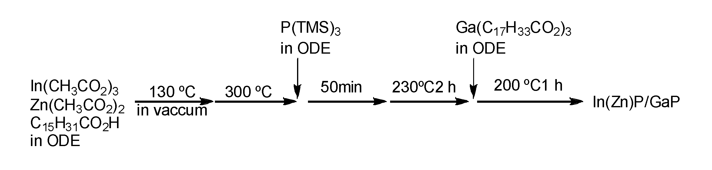
乾燥窒素で充填されたグローブボックス中、200ml三口フラスコに、オクタデセン(20mL)、酢酸インジウム(88mg)、酢酸亜鉛(28mg)、パルミチン酸(308mg)を加え、130℃で30分間真空脱気を行った。本実験で使用する1-オクタデセンは水素化カルシウムから減圧蒸留し、カールフィッシャー法で算出した水分量が6ppmであることを確認したものを用いた。反応容器を300℃に加熱し、トリス(トリメチルシリル)ホスフィン[P(TMS)3]をオクタデセン[ODE、非配位性溶媒]に溶解した溶液(P(TMS)3濃度:45mM)4mlを素早く添加した。添加後50分間かけ230℃まで放冷し、230℃で2時間反応させ、In(Zn)P粒子の分散液を得た。この分散液をサンプリングし、HR-TEM(高分解能透過電子顕微鏡)を用いて粒径を測定した結果、In(Zn)P粒子の平均粒径は3nmであった。続いて200℃に放冷後、ガリウム溶液(塩化ガリウム(19mg)、オレイン酸(119μl)、オクタデセン(5ml)の混合物を90℃で1時間加熱した溶液[スキーム中、Ga(C17H33CO2)3で示した])4.3mLを加え、200℃で1時間反応させてIn(Zn)P粒子表層にGaを導入し、室温まで放冷した。得られた量子ドットの平均粒径は4nmであった。この量子ドット分散液をトルエンで5倍に希釈し、蛍光スペクトル(日立ハイテクサイエンス社製F-7000、励起波長450nm)を測定し、発光極大、発光ピークの半値幅、及び量子収率を測定した。結果を下記表1に示す。
[実施例2]
実施例1において、含水率6ppmの1-オクタデセンに代えて、含水率23ppmの1-オクタデセンを用いたこと以外は、実施例1と同様にして量子ドットを得、実施例1と同様にして発光極大、発光ピークの半値幅及び量子収率を測定した。結果を下記表1に示す。実施例2において、得られた量子ドットの平均粒径は4nmであった。
実施例1において、含水率6ppmの1-オクタデセンに代えて、含水率23ppmの1-オクタデセンを用いたこと以外は、実施例1と同様にして量子ドットを得、実施例1と同様にして発光極大、発光ピークの半値幅及び量子収率を測定した。結果を下記表1に示す。実施例2において、得られた量子ドットの平均粒径は4nmであった。
[実施例3]
実施例1において、含水率6ppmの1-オクタデセンに代えて、含水率14ppmの1-オクタデセンを用いたこと以外は、実施例1と同様にして量子ドットを得、実施例1と同様にして発光極大、発光ピークの半値幅及び量子収率を測定した。結果を下記表1に示す。実施例3において、得られた量子ドットの平均粒径は4nmであった。
実施例1において、含水率6ppmの1-オクタデセンに代えて、含水率14ppmの1-オクタデセンを用いたこと以外は、実施例1と同様にして量子ドットを得、実施例1と同様にして発光極大、発光ピークの半値幅及び量子収率を測定した。結果を下記表1に示す。実施例3において、得られた量子ドットの平均粒径は4nmであった。
[実施例4]
実施例1において、亜鉛溶液に用いた酢酸亜鉛を酢酸銅(II)に代えたこと以外は、実施例1と同様にして量子ドットを得、実施例1と同様にして発光極大、発光ピークの半値幅及び量子収率を測定した。結果を下記表1に示す。実施例4において、得られた量子ドットの平均粒径は6nmであった。
実施例1において、亜鉛溶液に用いた酢酸亜鉛を酢酸銅(II)に代えたこと以外は、実施例1と同様にして量子ドットを得、実施例1と同様にして発光極大、発光ピークの半値幅及び量子収率を測定した。結果を下記表1に示す。実施例4において、得られた量子ドットの平均粒径は6nmであった。
[実施例5]
実施例1において、亜鉛溶液を加えた後の反応条件:200℃で15分間を、90℃で15分間に代えたこと以外は、実施例1と同様にして量子ドットを得、実施例1と同様にして発光極大、発光ピークの半値幅及び量子収率を測定した。結果を下記表1に示す。実施例5において、得られた量子ドットの平均粒径は4nmであった。
実施例1において、亜鉛溶液を加えた後の反応条件:200℃で15分間を、90℃で15分間に代えたこと以外は、実施例1と同様にして量子ドットを得、実施例1と同様にして発光極大、発光ピークの半値幅及び量子収率を測定した。結果を下記表1に示す。実施例5において、得られた量子ドットの平均粒径は4nmであった。
[実施例6]
実施例1において、亜鉛溶液を加えた後の反応条件:200℃で15分間を、150℃で15分間に代えたこと以外は、実施例1と同様にして量子ドットを得、実施例1と同様にして発光極大、発光ピークの半値幅及び量子収率を測定した。結果を下記表1に示す。実施例6において、得られた量子ドットの平均粒径は4nmであった。
実施例1において、亜鉛溶液を加えた後の反応条件:200℃で15分間を、150℃で15分間に代えたこと以外は、実施例1と同様にして量子ドットを得、実施例1と同様にして発光極大、発光ピークの半値幅及び量子収率を測定した。結果を下記表1に示す。実施例6において、得られた量子ドットの平均粒径は4nmであった。
[実施例7]
実施例1において、1-オクタデセン(配位性溶媒)に代えて、ジフェニルエーテル(配位性溶媒)を用いたこと以外は、実施例1と同様にして量子ドットを得、実施例1と同様にして発光極大、発光ピークの半値幅及び量子収率を測定した。結果を下記表1に示す。実施例7において、得られた量子ドットの平均粒径は5nmであった。
実施例1において、1-オクタデセン(配位性溶媒)に代えて、ジフェニルエーテル(配位性溶媒)を用いたこと以外は、実施例1と同様にして量子ドットを得、実施例1と同様にして発光極大、発光ピークの半値幅及び量子収率を測定した。結果を下記表1に示す。実施例7において、得られた量子ドットの平均粒径は5nmであった。
[実施例8]
実施例1において、InP粒子形成の反応時間を調整してInP粒子の平均粒径を11nmとしたこと以外は、実施例1と同様にして量子ドットを得、実施例1と同様にして発光極大、発光ピークの半値幅及び量子収率を測定した。結果を下記表1に示す。実施例8において、得られた量子ドットの平均粒径は12nmであった。
実施例1において、InP粒子形成の反応時間を調整してInP粒子の平均粒径を11nmとしたこと以外は、実施例1と同様にして量子ドットを得、実施例1と同様にして発光極大、発光ピークの半値幅及び量子収率を測定した。結果を下記表1に示す。実施例8において、得られた量子ドットの平均粒径は12nmであった。
[比較例2]
比較例1において、酢酸亜鉛に代えて酢酸銅(II)を用いたこと以外は、比較例1と同様にして量子ドットを得、比較例1と同様にして発光極大、発光ピークの半値幅及び量子収率を測定した。結果を下記表1に示す。比較例2において、得られた量子ドットの平均粒径は6nmであった。
比較例1において、酢酸亜鉛に代えて酢酸銅(II)を用いたこと以外は、比較例1と同様にして量子ドットを得、比較例1と同様にして発光極大、発光ピークの半値幅及び量子収率を測定した。結果を下記表1に示す。比較例2において、得られた量子ドットの平均粒径は6nmであった。
[比較例3]
比較例1において、1-オクタデセン(配位性溶媒)に代えて、ジフェニルエーテル(配位性溶媒)を用いたこと以外は、比較例1と同様にして量子ドットを得、比較例1と同様にして発光極大、発光ピークの半値幅及び量子収率を測定した。結果を下記表1に示す。比較例3において、得られた量子ドットの平均粒径は4nmであった。
比較例1において、1-オクタデセン(配位性溶媒)に代えて、ジフェニルエーテル(配位性溶媒)を用いたこと以外は、比較例1と同様にして量子ドットを得、比較例1と同様にして発光極大、発光ピークの半値幅及び量子収率を測定した。結果を下記表1に示す。比較例3において、得られた量子ドットの平均粒径は4nmであった。
[実施例9]
実施例1で得られた量子ドットにさらにZnSシェル層を形成させた。より詳細には、実施例1においてガリウム溶液を加えて200℃で1時間反応させた後、240℃に加熱し、亜鉛溶液(酢酸亜鉛(66mg)、パルミチン酸(185mg)、オクタデセン(15ml)の混合物を130℃で30分間真空脱気した溶液)と1-ドデカンチオール182mgとの混合物10mLを加え、240℃で6時間反応させ、室温まで放冷した。この量子ドット分散液をトルエンで5倍に希釈し、実施例1と同様にして発光極大、発光ピークの半値幅及び量子収率を測定した。結果を下記表1に示す。実施例9において、得られた量子ドットのシェル層を含めた平均粒径は、5nmであった。
実施例1で得られた量子ドットにさらにZnSシェル層を形成させた。より詳細には、実施例1においてガリウム溶液を加えて200℃で1時間反応させた後、240℃に加熱し、亜鉛溶液(酢酸亜鉛(66mg)、パルミチン酸(185mg)、オクタデセン(15ml)の混合物を130℃で30分間真空脱気した溶液)と1-ドデカンチオール182mgとの混合物10mLを加え、240℃で6時間反応させ、室温まで放冷した。この量子ドット分散液をトルエンで5倍に希釈し、実施例1と同様にして発光極大、発光ピークの半値幅及び量子収率を測定した。結果を下記表1に示す。実施例9において、得られた量子ドットのシェル層を含めた平均粒径は、5nmであった。
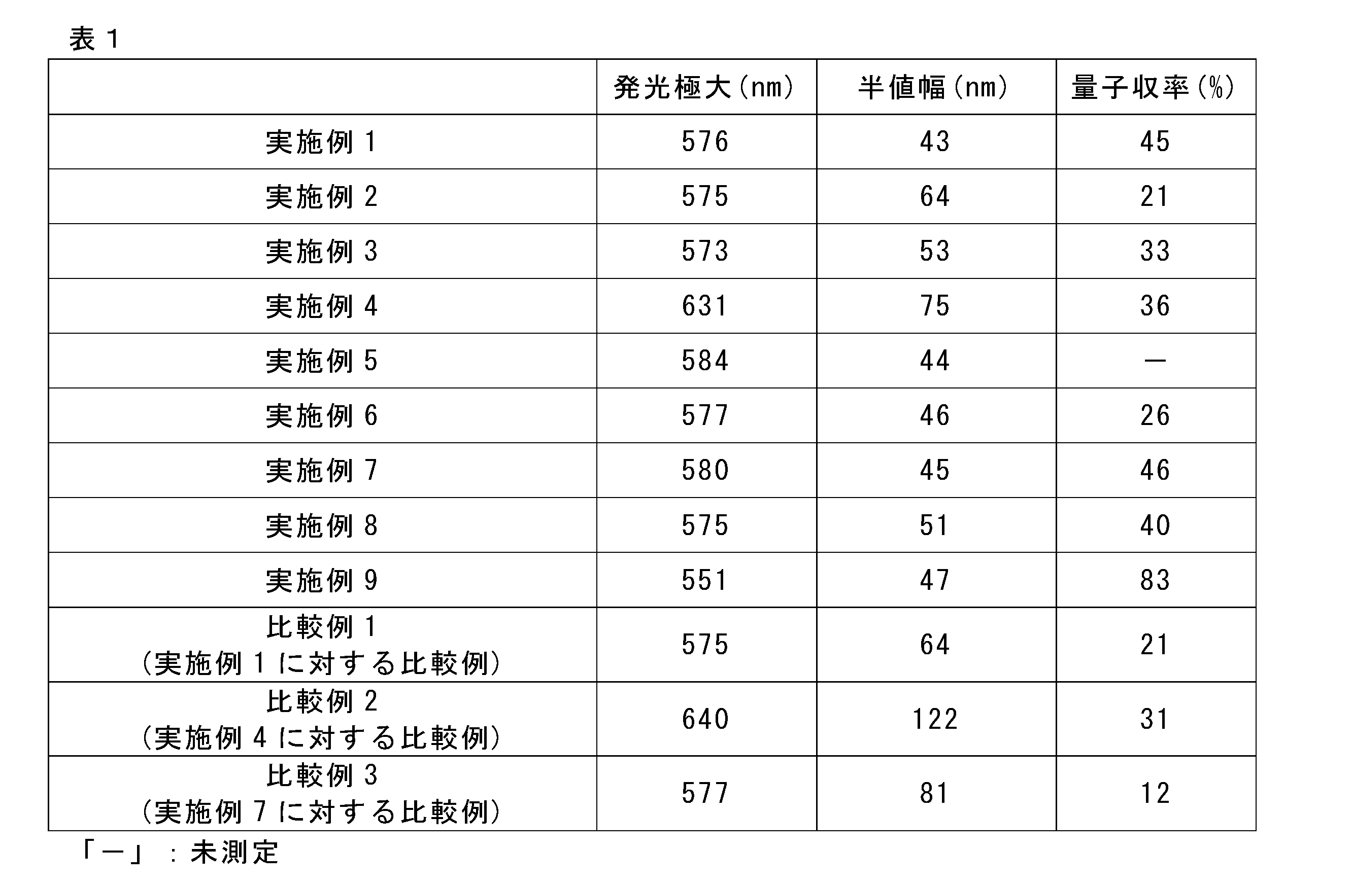
上記表1に示されるように、InP粒子の調製においてZnをドープさせた場合(比較例1、ナノ粒子としてIn(Zn)Pを用いた場合)、InP粒子の調製においてZnをドープさせず、InP粒子形成後に表層にZnを導入した場合(実施例1)に比べて、発光ピークの半値幅が大きく広がり、ブロードな発光特性を示した。また、この比較例1の量子収率は、実施例1に比べて半分以下にまで低下する結果となった。
この傾向は、溶媒の種類によらずに認められた(比較例3と実施例7との比較)。
この傾向は、溶媒の種類によらずに認められた(比較例3と実施例7との比較)。
また、InP粒子の調製においてCuをドープさせた場合(比較例2、ナノ粒子としてIn(Cu)Pを用いた場合)も、InP粒子の調製においてCuをドープさせず、InP粒子形成後に表層にCuを導入した場合(実施例4)に比べて、発光ピークの半値幅が大きく広がり、ブロードな発光特性を示す結果となった。また、この比較例2の量子収率は、実施例4に比べて低くなることもわかった。
また表1の実施例1と実施例2~7との比較から、溶媒の含水率が高まると発光ピークの半値幅が広がり、量子収率も低下する傾向があること(実施例2、3)、金属a1の種類によって発光ピーク波長が変化すること(実施例4)、工程(A1)の反応温度を下げると半値幅がわずかに広がり、また量子収率が低下する傾向にあること(実施例5、6)、溶媒として配位性溶媒を用いると半値幅と量子収率においてわずかながら劣る傾向にあること(実施例7)もわかる。ただし、これらの各実施例において、工程(A1)に用いるナノ粒子として不純物原子をドープさせたもの(In(Zn)P又はIn(Cu)P)を用いた場合との比較においては、上記各実施例はいずれもよりシャープな発光ピークを示し、量子収率にも優れるものとなる。
本発明をその実施態様とともに説明したが、我々は特に指定しない限り我々の発明を説明のどの細部においても限定しようとするものではなく、添付の請求の範囲に示した発明の精神と範囲に反することなく幅広く解釈されるべきであると考える。
本願は、2016年3月28日に日本国で特許出願された特願2016-063417に基づく優先権を主張するものであり、これはここに参照してその内容を本明細書の記載の一部として取り込む。
Claims (14)
- 下記工程(A1)及び(B1)を含む、半導体量子ドットの製造方法:
(A1)PbS、PbSe、InN、InAs、InSb及びInPからなる群から選ばれる少なくとも1種の化合物半導体からなるナノ粒子と、下記金属群[a]から選ばれる少なくとも1種の金属a1の塩とを反応させて、前記ナノ粒子表層に金属a1を導入する工程;及び
(B1)表層に金属a1が導入された前記ナノ粒子と、下記金属群[b]から選ばれる少なくとも1種の金属b1の塩とを反応させて、前記ナノ粒子表層に金属b1を導入する工程。
金属群[a]:
Ca、Sc、Ti、V、Cr、Mn、Fe、Co、Ni、Cu及びZn。
金属群[b]:
Ga及びGe。 - 前記工程(A1)で用いるPbS、PbSe、InN、InAs、InSb及びInPからなる群から選ばれる少なくとも1種の化合物半導体からなるナノ粒子の平均粒径が1~10nmである、請求項1に記載の半導体量子ドットの製造方法。
- 前記工程(A1)における反応温度を100℃以上とする、請求項1又は2に記載の半導体量子ドットの製造方法。
- 前記工程(B1)における反応温度を100℃以上とする、請求項1~3のいずれか1項に記載の半導体量子ドットの製造方法。
- 前記工程(A1)及び(B1)における反応を非配位性溶媒中で行う、請求項1~4のいずれか1項に記載の半導体量子ドットの製造方法。
- 前記溶媒の含水率が10ppm以下である、請求項5に記載の半導体量子ドットの製造方法。
- 前記工程(A1)及び(B1)における各反応を配位性化合物の存在下で行う、請求項1~6のいずれか1項に記載の半導体量子ドットの製造方法。
- 前記金属a1がZnであり、前記金属b1がGaである、請求項1~7のいずれか1項に記載の半導体量子ドットの製造方法。
- 前記工程(A1)で用いるナノ粒子がInPである、請求項1~8のいずれか1項に記載の半導体量子ドットの製造方法。
- 前記工程(B1)で得られた、表層に金属b1が導入されたナノ粒子表層に、シェル層を形成する工程を含む、請求項1~9のいずれか1項に記載の半導体量子ドットの製造方法。
- 前記シェル層がZnS、ZnO、ZnSe、ZnSeXS1-X、ZnTe又はCuOである、請求項10に記載の半導体量子ドットの製造方法。但し、0<X<1である。
- PbS、PbSe、InN、InAs、InSb及びInPからなる群から選ばれる少なくとも1種の化合物半導体からなるナノ粒子の表層に、下記金属群[a]から選ばれる少なくとも1種の金属a1、及び/又は、下記金属群[b]から選ばれる少なくとも1種の金属b1が導入された構造を有する半導体量子ドット。
金属群[a]:
Ca、Sc、Ti、V、Cr、Mn、Fe、Co、Ni、Cu及びZn。
金属群[b]:
Ga及びGe。 - 前記の金属a1及び/又は金属b1が導入された表層にシェル層を有してなる、請求項12に記載の半導体量子ドット。
- 前記シェル層がZnS、ZnO、ZnSe、ZnSeXS1-X、ZnTe、又はCuOである、請求項13に記載の半導体量子ドット。
Priority Applications (2)
| Application Number | Priority Date | Filing Date | Title |
|---|---|---|---|
| JP2018509066A JP6651002B2 (ja) | 2016-03-28 | 2017-03-17 | 半導体量子ドットの製造方法及び半導体量子ドット |
| US16/137,504 US10947112B2 (en) | 2016-03-28 | 2018-09-20 | Method of manufacturing semiconductor quantum dot and semiconductor quantum dot |
Applications Claiming Priority (2)
| Application Number | Priority Date | Filing Date | Title |
|---|---|---|---|
| JP2016063417 | 2016-03-28 | ||
| JP2016-063417 | 2016-03-28 |
Related Child Applications (1)
| Application Number | Title | Priority Date | Filing Date |
|---|---|---|---|
| US16/137,504 Continuation US10947112B2 (en) | 2016-03-28 | 2018-09-20 | Method of manufacturing semiconductor quantum dot and semiconductor quantum dot |
Publications (1)
| Publication Number | Publication Date |
|---|---|
| WO2017169932A1 true WO2017169932A1 (ja) | 2017-10-05 |
Family
ID=59965214
Family Applications (1)
| Application Number | Title | Priority Date | Filing Date |
|---|---|---|---|
| PCT/JP2017/011037 Ceased WO2017169932A1 (ja) | 2016-03-28 | 2017-03-17 | 半導体量子ドットの製造方法及び半導体量子ドット |
Country Status (3)
| Country | Link |
|---|---|
| US (1) | US10947112B2 (ja) |
| JP (1) | JP6651002B2 (ja) |
| WO (1) | WO2017169932A1 (ja) |
Cited By (2)
| Publication number | Priority date | Publication date | Assignee | Title |
|---|---|---|---|---|
| KR20220139349A (ko) * | 2020-02-21 | 2022-10-14 | 쇼에이 가가쿠 가부시키가이샤 | 코어/셸형 반도체 나노 입자의 제조 방법 |
| US11802239B2 (en) | 2020-03-21 | 2023-10-31 | Samsung Display Co., Ltd. | Quantum dot, method of preparing quantum dot, optical member including quantum dot, and electronic device including quantum dot |
Families Citing this family (1)
| Publication number | Priority date | Publication date | Assignee | Title |
|---|---|---|---|---|
| CN115232622B (zh) * | 2022-08-24 | 2023-06-06 | 合肥福纳科技有限公司 | 非Cd系量子点的制备方法及制备得到的非Cd系量子点 |
Citations (4)
| Publication number | Priority date | Publication date | Assignee | Title |
|---|---|---|---|---|
| JP2007173755A (ja) * | 2005-11-28 | 2007-07-05 | Kyocera Corp | 蛍光体粒子および波長変換器ならびに発光装置 |
| JP2010106119A (ja) * | 2008-10-29 | 2010-05-13 | Sharp Corp | 半導体ナノ粒子蛍光体 |
| JP2010155872A (ja) * | 2008-12-26 | 2010-07-15 | Sharp Corp | 半導体ナノ粒子蛍光体 |
| JP2012087220A (ja) * | 2010-10-20 | 2012-05-10 | Sharp Corp | 半導体ナノ粒子蛍光体 |
Family Cites Families (1)
| Publication number | Priority date | Publication date | Assignee | Title |
|---|---|---|---|---|
| US11142692B2 (en) * | 2015-07-28 | 2021-10-12 | The Regents Of The University Of California | Capped co-doped core/shell nanocrystals for visible light emission |
-
2017
- 2017-03-17 JP JP2018509066A patent/JP6651002B2/ja active Active
- 2017-03-17 WO PCT/JP2017/011037 patent/WO2017169932A1/ja not_active Ceased
-
2018
- 2018-09-20 US US16/137,504 patent/US10947112B2/en active Active
Patent Citations (4)
| Publication number | Priority date | Publication date | Assignee | Title |
|---|---|---|---|---|
| JP2007173755A (ja) * | 2005-11-28 | 2007-07-05 | Kyocera Corp | 蛍光体粒子および波長変換器ならびに発光装置 |
| JP2010106119A (ja) * | 2008-10-29 | 2010-05-13 | Sharp Corp | 半導体ナノ粒子蛍光体 |
| JP2010155872A (ja) * | 2008-12-26 | 2010-07-15 | Sharp Corp | 半導体ナノ粒子蛍光体 |
| JP2012087220A (ja) * | 2010-10-20 | 2012-05-10 | Sharp Corp | 半導体ナノ粒子蛍光体 |
Cited By (3)
| Publication number | Priority date | Publication date | Assignee | Title |
|---|---|---|---|---|
| KR20220139349A (ko) * | 2020-02-21 | 2022-10-14 | 쇼에이 가가쿠 가부시키가이샤 | 코어/셸형 반도체 나노 입자의 제조 방법 |
| KR102786180B1 (ko) | 2020-02-21 | 2025-03-26 | 쇼에이 가가쿠 가부시키가이샤 | 코어/셸형 반도체 나노 입자의 제조 방법 |
| US11802239B2 (en) | 2020-03-21 | 2023-10-31 | Samsung Display Co., Ltd. | Quantum dot, method of preparing quantum dot, optical member including quantum dot, and electronic device including quantum dot |
Also Published As
| Publication number | Publication date |
|---|---|
| JPWO2017169932A1 (ja) | 2019-02-14 |
| US10947112B2 (en) | 2021-03-16 |
| JP6651002B2 (ja) | 2020-02-19 |
| US20190027562A1 (en) | 2019-01-24 |
Similar Documents
| Publication | Publication Date | Title |
|---|---|---|
| Pu et al. | Highly reactive, flexible yet green Se precursor for metal selenide nanocrystals: Se-octadecene suspension (Se-SUS) | |
| CN108239535B (zh) | 具有核-壳结构的Ga掺杂的InP量子点及其制备方法 | |
| TW201313877A (zh) | 以週期分類第ib、iib、iiia、via族元素為基礎之強螢光半導體核-殼奈米粒子的合成 | |
| TWI901604B (zh) | 量子點及其製造方法 | |
| US12528986B2 (en) | Core-shell type quantum dot and method for manufacturing core-shell type quantum dot | |
| US10947112B2 (en) | Method of manufacturing semiconductor quantum dot and semiconductor quantum dot | |
| JPWO2017204193A1 (ja) | コアシェル粒子、コアシェル粒子の製造方法およびフィルム | |
| JP6651024B2 (ja) | 半導体量子ドットの製造方法 | |
| US11459243B2 (en) | Core shell particle, method of producing core shell particle, and film | |
| Liu et al. | A general and rapid room-temperature synthesis approach for metal sulphide nanocrystals with tunable properties | |
| JP2020176044A (ja) | InP量子ドット前駆体の製造方法及びInP系量子ドットの製造方法 | |
| WO2016185932A1 (ja) | コアシェル粒子、コアシェル粒子の製造方法およびフィルム | |
| JP7475839B2 (ja) | 亜鉛含有ナノ粒子の合成方法 | |
| JP6630446B2 (ja) | コアシェル粒子、コアシェル粒子の製造方法およびフィルム | |
| US11492252B2 (en) | Method for producing group III-V semiconductor nanoparticle, method for producing group III-V semiconductor quantum dot, and flow reaction system | |
| WO2020213365A1 (ja) | InP量子ドット前駆体の製造方法及びInP系量子ドットの製造方法 | |
| JP6595854B2 (ja) | テルル化合物ナノ粒子の製造方法 | |
| JP7508217B2 (ja) | InP量子ドット前駆体の製造方法及びInP系量子ドットの製造方法 | |
| JP2019151832A (ja) | コアシェル型量子ドット分散液の製造方法及び量子ドット分散液の製造方法 | |
| JP7475840B2 (ja) | ウルツ鉱型硫化物ナノ粒子の合成方法 | |
| KR102696629B1 (ko) | 청색발광 나노입자의 제조방법 | |
| CN108929690A (zh) | 一种合金纳米晶的制备方法 | |
| US20240023357A1 (en) | Quantum dot and method for preparing the same | |
| Hu et al. | Epitaxial Growth of Spherical Monodisperse ZnSe Quantum Dots: Roles of Additives and Precursors | |
| TW202432920A (zh) | Iii-v奈米晶體之可擴展合成 |
Legal Events
| Date | Code | Title | Description |
|---|---|---|---|
| WWE | Wipo information: entry into national phase |
Ref document number: 2018509066 Country of ref document: JP |
|
| NENP | Non-entry into the national phase |
Ref country code: DE |
|
| 121 | Ep: the epo has been informed by wipo that ep was designated in this application |
Ref document number: 17774473 Country of ref document: EP Kind code of ref document: A1 |
|
| 122 | Ep: pct application non-entry in european phase |
Ref document number: 17774473 Country of ref document: EP Kind code of ref document: A1 |