WO2017169686A1 - 電圧変換装置及び電圧変換方法 - Google Patents
電圧変換装置及び電圧変換方法 Download PDFInfo
- Publication number
- WO2017169686A1 WO2017169686A1 PCT/JP2017/009928 JP2017009928W WO2017169686A1 WO 2017169686 A1 WO2017169686 A1 WO 2017169686A1 JP 2017009928 W JP2017009928 W JP 2017009928W WO 2017169686 A1 WO2017169686 A1 WO 2017169686A1
- Authority
- WO
- WIPO (PCT)
- Prior art keywords
- switching
- pwm signal
- time
- frequency
- switching frequency
- Prior art date
- Legal status (The legal status is an assumption and is not a legal conclusion. Google has not performed a legal analysis and makes no representation as to the accuracy of the status listed.)
- Ceased
Links
Images



Classifications
-
- H—ELECTRICITY
- H03—ELECTRONIC CIRCUITRY
- H03K—PULSE TECHNIQUE
- H03K3/00—Circuits for generating electric pulses; Monostable, bistable or multistable circuits
- H03K3/01—Details
- H03K3/017—Adjustment of width or dutycycle of pulses
-
- H—ELECTRICITY
- H03—ELECTRONIC CIRCUITRY
- H03K—PULSE TECHNIQUE
- H03K7/00—Modulating pulses with a continuously-variable modulating signal
- H03K7/08—Duration or width modulation ; Duty cycle modulation
-
- H—ELECTRICITY
- H02—GENERATION; CONVERSION OR DISTRIBUTION OF ELECTRIC POWER
- H02M—APPARATUS FOR CONVERSION BETWEEN AC AND AC, BETWEEN AC AND DC, OR BETWEEN DC AND DC, AND FOR USE WITH MAINS OR SIMILAR POWER SUPPLY SYSTEMS; CONVERSION OF DC OR AC INPUT POWER INTO SURGE OUTPUT POWER; CONTROL OR REGULATION THEREOF
- H02M3/00—Conversion of DC power input into DC power output
- H02M3/02—Conversion of DC power input into DC power output without intermediate conversion into AC
- H02M3/04—Conversion of DC power input into DC power output without intermediate conversion into AC by static converters
- H02M3/10—Conversion of DC power input into DC power output without intermediate conversion into AC by static converters using discharge tubes with control electrode or semiconductor devices with control electrode
- H02M3/145—Conversion of DC power input into DC power output without intermediate conversion into AC by static converters using discharge tubes with control electrode or semiconductor devices with control electrode using devices of a triode or transistor type requiring continuous application of a control signal
- H02M3/155—Conversion of DC power input into DC power output without intermediate conversion into AC by static converters using discharge tubes with control electrode or semiconductor devices with control electrode using devices of a triode or transistor type requiring continuous application of a control signal using semiconductor devices only
-
- H—ELECTRICITY
- H03—ELECTRONIC CIRCUITRY
- H03K—PULSE TECHNIQUE
- H03K17/00—Electronic switching or gating, i.e. not by contact-making and –breaking
- H03K17/51—Electronic switching or gating, i.e. not by contact-making and –breaking characterised by the components used
- H03K17/56—Electronic switching or gating, i.e. not by contact-making and –breaking characterised by the components used by the use, as active elements, of semiconductor devices
- H03K17/60—Electronic switching or gating, i.e. not by contact-making and –breaking characterised by the components used by the use, as active elements, of semiconductor devices the devices being bipolar transistors
- H03K17/64—Electronic switching or gating, i.e. not by contact-making and –breaking characterised by the components used by the use, as active elements, of semiconductor devices the devices being bipolar transistors having inductive loads
Definitions
- the present invention relates to a voltage conversion device and a voltage conversion method.
- This application claims priority based on Japanese Patent Application No. 2016-66759 filed on Mar. 29, 2016, and incorporates all the description items described in the above Japanese application.
- a DC / DC converter as a power circuit for supplying power to a load.
- This DC / DC converter includes a switching element and an inductor, and switches the switching element on / off based on a PWM signal, thereby transforming (boosting or stepping down) the voltage from the battery and outputting the voltage to a load.
- the voltage from the battery can be transformed (step-up or step-down) and a constant voltage can be applied to the load.
- a voltage mode control method that feeds back the output voltage As a control method for stabilizing the output voltage of the DC / DC converter, a voltage mode control method that feeds back the output voltage, a current mode control method that feeds back the output current in addition to the output voltage, and the like are known.
- Patent Document 1 discloses a technique for switching a switching frequency for a switching element according to an output current in order to realize a DC / DC converter that can suppress ripple current and maintain high transformation efficiency.
- a voltage conversion device includes a switching element, an inductor, and a drive circuit, and drives the on / off state of the switching element with a PWM signal by the drive circuit, thereby converting an input voltage.
- switching means for switching the switching frequency by the drive circuit according to the magnitude of the output current to the load, and the switching by the switching means
- changing means for changing the waveform of the PWM signal is provided, and the changing means changes the ON time of the PWM signal and drives ON / OFF of the switching element.
- a voltage conversion method includes a switching element, an inductor, and a drive circuit, and the drive circuit drives the on / off state of the switching element with a PWM signal so that an input voltage is obtained.
- the voltage conversion method by the voltage conversion device that generates the inductor current, transforms it, and outputs it to the load, when switching the switching frequency by the drive circuit according to the magnitude of the output current to the load, The waveform is changed, the on time of the PWM signal is changed, and the on / off of the switching element is driven.
- FIG. 10 is a timing chart showing a relationship among a switching frequency, a PWM signal, and an inductor current according to Modification 2. It is a timing chart which shows the relationship between the switching frequency which concerns on 3rd Embodiment of this invention, a PWM signal, and an inductor current. It is a timing chart which shows the relationship between the switching frequency which concerns on 4th Embodiment of this invention, a PWM signal, and an inductor current. It is a timing chart which shows the relationship between the switching frequency which concerns on 5th Embodiment of this invention, a PWM signal, and an inductor current. It is a timing chart which shows the relationship between the switching frequency which concerns on 6th Embodiment of this invention, a PWM signal, and an inductor current.
- the present invention has been made in view of such circumstances, and an object of the present invention is to provide a voltage that can suppress fluctuations in the output voltage when switching the switching frequency and can stably output a constant voltage to a load.
- an object of the present invention is to provide a voltage that can suppress fluctuations in the output voltage when switching the switching frequency and can stably output a constant voltage to a load.
- a voltage converter includes a switching element, an inductor, and a drive circuit, and is input by driving on / off of the switching element with a PWM signal by the drive circuit.
- the switching means for switching the switching frequency by the drive circuit according to the magnitude of the output current to the load, and the switching means
- the switching unit includes a changing unit that changes a waveform of the PWM signal, and the changing unit changes an on time of the PWM signal and drives on / off of the switching element.
- a voltage conversion method includes a switching element, an inductor, and a drive circuit, and is input by driving on / off of the switching element with a PWM signal by the drive circuit.
- the voltage conversion method by the voltage conversion device that generates an inductor current and transforms and outputs the voltage to the load, when switching the switching frequency by the drive circuit according to the magnitude of the output current to the load, The waveform of the PWM signal is changed, the on time of the PWM signal is changed, and the on / off of the switching element is driven.
- the waveform of the PWM signal when switching to increase / decrease the switching frequency for the switching element, the waveform of the PWM signal is changed. This change suppresses a decrease / increase in the average value of the inductor current after switching the switching frequency, and suppresses fluctuations in the output voltage after switching the switching frequency.
- the changing unit may determine the amount of change in the waveform of the PWM signal so that the lower limit value of the inductor current is the same immediately after the change of the waveform and the steady state after the switching of the switching frequency. preferable.
- the amount of change in the waveform of the PWM signal is determined so that the lower limit value of the inductor current matches between the state immediately after the change of the waveform and the steady state after the switching of the switching frequency. Therefore, when switching to increase / decrease the switching frequency, the average value of the inductor current after switching can be efficiently suppressed.
- the change amount of the waveform of the PWM signal changed by the changing means includes at least one of an on time of the PWM signal and a duty ratio of the PWM signal.
- the amount of change in the waveform of the PWM signal to be changed is at least one of the on time of the PWM signal and the duty ratio of the PWM signal. Therefore, fluctuations in the output voltage after switching the switching frequency can be reliably suppressed.
- the changing unit changes a waveform in only one cycle of the PWM signal immediately after switching of the switching frequency or immediately before switching.
- the waveform is changed by one cycle of the PWM signal immediately after switching of the switching frequency or immediately before switching. Therefore, fluctuations in the output voltage can be quickly suppressed after switching the switching frequency.
- the changing unit changes a waveform in a plurality of cycles of the PWM signal immediately after switching of the switching frequency or immediately before switching.
- the waveform is changed over a plurality of periods of the PWM signal immediately after switching of the switching frequency or immediately before switching. Therefore, fluctuations in the output voltage can be suppressed without significant fluctuations after switching the switching frequency.
- the duty ratio of the PWM signal immediately after switching is larger than the duty ratio of the PWM signal before switching (or after switching).
- the duty ratio of the PWM signal immediately after switching may be smaller than the duty ratio of the PWM signal before switching (or after switching). preferable.
- the duty ratio of the PWM signal immediately after switching is changed from before switching (or after switching) according to the switching frequency high / low. Increase / decrease. Therefore, fluctuations in the output voltage after switching the switching frequency can be reliably suppressed.
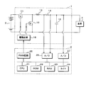
- FIG. 1 is a block diagram illustrating a configuration example of the voltage conversion device according to the first embodiment of the present invention
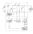
- FIG. 2 is a block diagram illustrating a functional configuration of the control unit 2 in the voltage conversion device.
- the voltage converter shown in FIG. 1 includes, for example, a DC / DC converter 1 that steps down the voltage of an external battery 3 and supplies the voltage to a load 4 and a control unit 2 that supplies a PWM signal to the DC / DC converter 1.
- the DC / DC converter 1 includes a switching element 11 having one end connected to the battery 3, a second switching element 12 and an inductor 13 each having one end connected to the other end of the switching element 11, and the other end of the inductor 13. And a capacitor 15 connected between the other end of the resistor 14 and the ground potential. The other end of the second switching element 12 is connected to the ground potential.
- the load 4 is connected across the capacitor 15.
- the switching element 11 and the second switching element 12 are, for example, N-channel MOSFETs each having one end as a drain.
- the DC / DC converter 1 also includes a drive circuit 16 that provides a drive signal for driving the switching element 11 and the second switching element 12 on / off.
- the drive circuit 16 supplies the PWM signal supplied from the control unit 2 and a PWM signal complementary to the PWM signal to the gates of the switching element 11 and the second switching element 12.
- the control unit 2 has a CPU 21, and the CPU 21 is connected to each other by a ROM 22 for storing information such as a program, a RAM 23 for storing temporarily generated information, and a timer 24 for measuring various times such as a PWM control cycle. Has been.
- the CPU 21 also includes a PWM circuit 25 that generates a PWM signal to be supplied to the drive circuit 16, and an A / D conversion circuit that detects the voltage across the resistor 14 and converts the current flowing through the resistor 14 into a digital current value. 26 and an A / D conversion circuit 27 for converting the voltage across the capacitor 15 into a digital voltage value are connected by a bus.
- control unit 2 realizes the function of the voltage loop controller 28 for controlling the output voltage output from the DC / DC converter 1 to the load 4 by a so-called voltage mode control method.
- the symbol “ ⁇ ” in the figure represents a subtractor.
- the voltage loop controller 28 is based on the deviation obtained by subtracting the digital voltage value Vo obtained by converting the output voltage output to the load 4 by the A / D conversion circuit 27 from the target voltage value Vref (ON time of the PWM signal ( Hereinafter, it is simply referred to as an on-time unless otherwise specified) and is output to the PWM circuit 25.
- the PWM circuit 25 generates a PWM signal having a duty ratio corresponding to a given on time.
- switching with respect to the switching element 11 and the second switching element 12 is performed according to the magnitude of the output current to the load 4 so that the voltage conversion efficiency is good.
- the frequency is switched. For example, when the output current is 20 A or more, the switching frequency is 150 kHz, and when the output current is less than 20 A, the switching frequency is 100 kHz.
- the ON time calculated by the voltage loop controller 28 is also switched. However, unless the duty ratio is corrected, the duty ratio of the PWM signal generated by the PWM circuit 25 does not change (described later). The same applies to other embodiments and modified examples).
- switching of the switching frequency (hereinafter also simply referred to as switching) is performed by changing (hereinafter also referred to as correction) the waveform of the PWM signal immediately after switching of the switching frequency. Such variations in output voltage that occur later are suppressed.
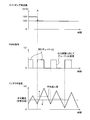
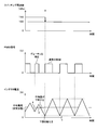
- FIG. 3 is a timing chart showing the relationship between the switching frequency, the PWM signal, and the inductor current according to the comparative example.
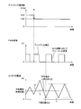
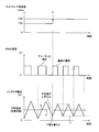
- FIG. 4 shows the relationship between the switching frequency, the PWM signal, and the inductor current according to the first embodiment of the present invention. It is a timing chart which shows. In each of the three timing diagrams shown in FIGS. 3 and 4, the horizontal axis is the same time axis.
- FIG. 3 shows a comparative example (conventional example) in which no change is made as in the present invention
- FIG. 4 shows an example according to the first embodiment of the present invention. In both examples, at timing A, the switching frequency is switched from 150 kHz to 100 kHz.
- the duty ratio in the PWM signal immediately after switching is the same as that before switching and is not changed. Therefore, the inductor current immediately after switching is increased, and the average value (represented by the broken line a) is higher than the average value in the steady state (represented by the solid line b). As a result, the output voltage varies greatly.
- a change in the inductor current accompanying switching of the switching frequency is predicted, and the lower limit value of the inductor current immediately after the switching is expressed as a lower limit value in a steady state (represented by a broken line c).
- the duty ratio in one cycle of the PWM signal immediately after switching is changed so as to coincide with (1).
- the lower limit value of the inductor current is matched between the cycle in which the duty ratio is changed and each cycle in the steady state after switching of the switching frequency.
- the amount of change in the waveform of the PWM signal immediately after the switching that is, the duty ratio after the change of the waveform immediately after switching the switching frequency (hereinafter simply referred to as “change”) and the specific value of the on-time after the change will be described. To do. Through a derivation process described later, it is derived that the changed duty ratio D ′ is calculated by the following equation (1).
- ON ′ ⁇ ON ⁇ F1 ⁇ (1-ON ⁇ F1) ⁇ / (2 ⁇ F1) + ⁇ ON ⁇ F1 ⁇ (1 + ON ⁇ F1) ⁇ / (2 ⁇ F2) (2)
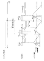
- FIG. 5 is a timing chart showing the relationship between the switching frequency, the PWM signal, and the inductor current before and after switching of the switching frequency for explaining the derivation of the change amount.
- the horizontal axis in the figure represents time. The process of deriving the above equation (1) will be described with reference to FIG.
- T ⁇ represents a part of the on-time immediately after switching of the switching frequency.
- the absolute value of the slope of the inductor current decrease period can be regarded as D / (1-D) times the slope of the inductor current increase period. . That is, the length of the decrease period of the inductor current during the period in which the increase / decrease in the inductor current cancels becomes (1 ⁇ D) / D times the length of the increase period of the inductor current. Is obtained by the following equation (3).
- D ′ Since the changed duty ratio D ′ is represented by on time / period, that is, on time ⁇ frequency, D ′ is obtained by the following equation (4).
- T ⁇ ⁇ D (1 + D ) / 2 ⁇ ⁇ (1 / F2) - (D 2/2) ⁇ (1 / F1) ⁇ (5)
- D ′ [(D / 2) ⁇ (1 / F1) + ⁇ D (1 + D) / 2 ⁇ ⁇ (1 / F2) - (D 2/2) ⁇ (1 / F1) ]
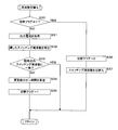
- FIG. 6 is a flowchart showing an operation procedure of the voltage converter.
- the operation shown in FIG. 6 is performed every control cycle of PWM control, and is executed by the CPU 21 in accordance with a control program stored in the ROM 22 in advance.
- step S1 In the operation of the voltage converter, the on-time calculation process (step S1), which is feedback control on the PWM signal based on the detected output voltage, and the necessity of switching of the switching frequency are determined. And a frequency switching process (step S2) in which the change amount is calculated and switched, and the CPU 21 executes these processes.
- step S1 the on-time calculation process (step S1) and the frequency switching process (step S2) will be described in detail.
- FIG. 7 is a flowchart showing the operation procedure of the on-time calculation process performed by the CPU 21 (subroutine of step S1).
- the CPU21 acquires the digital voltage value which converted the output voltage output to the load 4 with the A / D conversion circuit 27 (step S11). Next, the CPU 21 calculates the ON time by performing PID calculation so that the output voltage becomes the target voltage value (Vref) based on the acquired voltage value (Vo) of the output voltage (step S12). The CPU 21 sends the calculated on-time to the PWM circuit 25 (step S13) and ends the process. A PWM signal is generated in the PWM circuit 25 in accordance with the transmitted on-time.
- FIG. 8 is a flowchart showing the operation procedure of the frequency switching process performed by the CPU 21 (subroutine of step S2).
- the CPU 21 obtains a digital current value obtained by converting the output current output to the load 4 by the A / D conversion circuit 26 (step S21).
- CPU21 specifies the switching frequency suitable for the electric current value of the acquired output current (step S22). Specifically, the CPU 21 specifies the switching frequency as 150 kHz when the acquired current value is 20 A or more, and specifies the switching frequency as 100 kHz when the acquired current value is less than 20 A.
- the CPU 21 determines whether or not the identified switching frequency matches the current switching frequency (step S23). If they match (S23: YES), the CPU 21 ends the process.
- the CPU 21 follows the above-described equation (2), the ON time before the change, the current switching frequency (the switching frequency before the change), and the specified switching frequency (the change The on-time after the change is calculated using (switching frequency after) (step S24). Then, the CPU 21 switches the current switching frequency to the specified switching frequency (step S25), and ends the process.
- the on-time in the first period immediately after switching of the switching frequency of the PWM signal is the on-time calculated in step S24.
- the characteristics of the waveform of the PWM signal immediately after switching (on time or duty ratio) ) Can be suppressed, so that the increase in the average value of the inductor current after switching due to switching can be suppressed, and as a result, fluctuations in output voltage can be suppressed and the constant voltage can be stabilized. It is possible to output to the load 4.
- the first embodiment is a mode in which the switching frequency is switched to decrease from a high frequency to a low frequency
- the first modification is a mode in which the switching frequency is switched to increase from a low frequency to a high frequency.
- the modification 1 of 1st Embodiment of this invention is demonstrated.
- the configuration of the voltage conversion device according to Modification 1 is the same as the configuration of the voltage conversion device according to the first embodiment described above (FIGS. 1 and 2).
- FIG. 9 is a timing chart showing a relationship among the switching frequency, the PWM signal, and the inductor current according to the first modification.
- the same time axis is taken as the horizontal axis.
- the switching frequency is switched from 100 kHz to 150 kHz.
- a change in the inductor current accompanying switching of the switching frequency is predicted so that the lower limit value of the inductor current immediately after the switching coincides with the lower limit value in the steady state (represented by a broken line c).
- the duty ratio in one cycle of the PWM signal immediately after switching is changed.
- the lower limit value of the inductor current is matched between the cycle in which the duty ratio is changed and each cycle in the steady state after switching of the switching frequency.
- the ON time in one cycle of the PWM signal immediately after switching of the switching frequency is changed.
- the ON time in one cycle of the PWM signal immediately before switching of the switching frequency is changed.
- This second embodiment is suitable when PWM control is to be performed without special correction immediately after switching the switching frequency.
- FIG. 10 is a timing chart showing the relationship among the switching frequency, the PWM signal, and the inductor current according to the second embodiment of the present invention.
- the switching frequency is switched from 150 kHz to 100 kHz at timing A.
- the change in the inductor current accompanying switching of the switching frequency is predicted so that the lower limit value of the inductor current at the time of switching coincides with the lower limit value in the steady state (represented by a broken line c).
- the duty ratio in one cycle of the PWM signal immediately before switching is changed.
- the lower limit value of the inductor current is matched between the cycle in which the duty ratio is changed and each cycle in the steady state after switching of the switching frequency.
- correction is performed so that the duty ratio is smaller in one cycle of the PWM signal immediately before switching than in the previous cycle (that is, in each cycle after switching). Therefore, the inductor current in one cycle immediately before switching becomes small, and the average value (represented by a broken line d) is appropriately lowered with respect to the average value in a steady state (represented by a solid line e). As a result, an increase in the average value of the inductor current after switching is suppressed, and fluctuations in the output voltage after switching are suppressed.
- the change amount of the waveform in the PWM signal immediately before switching that is, the duty ratio after changing the waveform immediately before switching the switching frequency and the specific value of the ON time after changing will be described.
- the changed duty ratio D ′ is calculated by the following equation (6).
- ON ′ ⁇ ON ⁇ F1 ⁇ (3-ON ⁇ F1) ⁇ / (2 ⁇ F1) + ⁇ ON ⁇ F1 ⁇ (ON ⁇ F1-1) ⁇ / (2 ⁇ F2) (7)
- FIG. 11 is a timing chart showing the relationship between the switching frequency, the PWM signal, and the inductor current before and after switching of the switching frequency for explaining the derivation of the change amount.
- the horizontal axis in the figure represents time. The process of deriving the above calculation formula will be described with reference to FIG.
- the length of the inductor current decrease period during the period in which the increase / decrease in the inductor current cancels out is calculated as follows. Since the length of the increase period is (1 ⁇ D) / D times, the period 1 / F1 immediately before the switching is obtained by the following equation (8).
- D ′ is represented by on-time ⁇ frequency
- D ′ is obtained by the following equation (4) (re-displayed).
- T ⁇ ⁇ D (2-D) / 2 ⁇ ⁇ (1 / F1) + ⁇ D (D ⁇ 1) / 2 ⁇ ⁇ (1 / F2) ⁇ ⁇ ⁇ ⁇ ⁇ ⁇ ⁇ ⁇ ⁇ ⁇ ⁇ ⁇ ⁇ ⁇ ⁇ ⁇ ⁇ ⁇ ⁇ ⁇ ⁇ ⁇ ⁇ ⁇ ⁇ ⁇ ⁇ ⁇ ⁇ ⁇ ⁇ ⁇ ⁇ ⁇ ⁇ ⁇ ⁇ (9)
- D ′ [(D / 2) ⁇ (1 / F1) + ⁇ D (2-D) / 2 ⁇ ⁇ (1 / F1) + ⁇ D (D-1) / 2 ⁇ ⁇ (1 / F2)]
- ⁇ F1 ⁇ D (3-D) / 2 * (1 / F1) + D (D-1) / 2 * (1 / F2) ⁇ * F1
- FIG. 12 is a flowchart showing the operation procedure of the frequency switching process performed by the CPU 21 (subroutine of step S2).
- the switching flag in the figure is a flag indicating whether or not it is a cycle for switching the switching frequency, and the initial value is set to 0 and stored in the RAM 23. Since the processing from step S31 to S34 shown in FIG. 12 is the same as the processing from step S21 to S24 shown in FIG. 8 in the first embodiment, the description thereof will be simplified.
- the CPU 21 determines whether or not the switching flag is set to 1 (step S30). When the switching flag is not set to 1 (S30: NO), the CPU 21 acquires the output current output to the load 4 (step S31), and specifies a switching frequency suitable for the acquired output current (step S32). ).
- the CPU 21 determines whether or not the identified switching frequency matches the current switching frequency (step S33). If they match (S33: YES), the process is terminated.
- step S34 calculates the changed on-time according to the above-described equation (7) (step S34), sets the switching flag to 1 (step S35), and performs the process. finish.
- step S30 If the switching flag is set to 1 in step S30 (S30: YES), the CPU 21 clears the switching flag to 0 (step S36), and then switches the current switching frequency to the specified switching frequency (step S30). S37) The process ends.
- the waveform characteristics (ON time or duty ratio) immediately before switching are switched. ) Can be suppressed, so that the increase in the average value of the inductor current after switching due to switching can be suppressed, and as a result, fluctuations in output voltage can be suppressed and the constant voltage can be stabilized. It is possible to output to the load 4.
- D ′ calculated by the expression (6) may be less than 0, but in that case, D ′ is not limited. A numerical value close to 0 may be used.
- Modification 2 The second embodiment is a mode in which the switching frequency is switched to be lowered from a high frequency to a low frequency, whereas the second modification is a mode in which the switching frequency is switched to be raised from a low frequency to a high frequency.
- Modification 2 of the second embodiment of the present invention will be described.
- the configuration of the voltage conversion device according to Modification 2 is the same as the configuration of the voltage conversion device according to the first embodiment described above (FIGS. 1 and 2).
- FIG. 13 is a timing chart showing a relationship among the switching frequency, the PWM signal, and the inductor current according to the second modification.
- the switching frequency is switched from 100 kHz to 150 kHz at timing A.
- the change in the inductor current accompanying switching of the switching frequency is predicted so that the lower limit value of the inductor current at the time of switching coincides with the lower limit value in the steady state (represented by a broken line c).
- the duty ratio in one cycle of the PWM signal immediately before switching is changed.
- the lower limit value of the inductor current is matched between the cycle in which the duty ratio is changed and each cycle in the steady state after switching of the switching frequency.
- FIG. 14 is a timing chart showing the relationship among the switching frequency, the PWM signal, and the inductor current according to the third embodiment of the present invention.
- the same time axis is taken as the horizontal axis.
- the switching frequency is switched from 150 kHz to 100 kHz at timing A.
- the on-time is changed over two cycles immediately after switching of the switching frequency. That is, in the first cycle immediately after switching the switching frequency, the on-time is changed by x1 ⁇ s so that the upper limit value of the inductor current matches the upper limit value in the steady state, and in the second cycle, the lower limit value of the inductor current is steady.
- the on-time is changed by x2 ⁇ s so as to coincide with the lower limit value in the state, and normal control is performed from the third period onward.
- the upper limit value and the lower limit value of the inductor current are made to coincide with each other in the first period and the second period in which the duty ratio is changed and in each period in the steady state after switching the switching frequency.
- the time when the switching frequency is switched is t0, and the time when the inductor current coincides with the average current immediately after that is t1.
- the time when the inductor current sequentially matches the average current is set as t3, t5, t7, t9, t11, and the time when the maximum value and the minimum value are sequentially set is set as t2, t4, t6, t8, t10, t12.
- the time from time t1 to t2 corresponds to T ⁇ in FIG. 5, and the time from time t8 to t10 corresponds to D ⁇ 1 / F2 in FIG.
- the following equation (10) is established.
- the changed duty ratio D ′ is represented by the on-time ⁇ frequency, so that D ′ is obtained by the following equation (4) (reprinted).
- the duty ratio D ′ in the first cycle (from time t0 to t4) after switching of the switching frequency is obtained as the following equation (11).
- the amount of correction of the on time of the PWM signal from time t0 to t2 is obtained by multiplying the second term on the right-hand side modified last by the equation (11) by the period (1 / F2). It is.
- the switching frequency from 150 kHz to 100 kHz, that is, when F2 / F1 is smaller than 1
- the duty ratio immediately after switching is corrected so as to be smaller than before switching.
- x1 is a negative number
- the PWM signal ON time immediately after switching is corrected so as to be shorter than the ON time in the steady state after switching.
- the correction amount of the PWM signal in the second period (from time t4 to t8) after switching of the switching frequency will be described.
- the duty ratio D ′ is corrected to be smaller than D as shown in the equation (11), so that the time from time t2 to t4 is the normal control at the frequency F2. It becomes longer than the time from time t10 to t12, and the inductor current is further reduced by that amount.
- the time from time t3 to t4 in the first cycle is T3, the time from time t0 to t1 is (D / 2) ⁇ (1 / F1), as in FIG. Further, the time from the time t1 to the time t3 is (1/2) ⁇ (1 / F2) corresponding to a half of one cycle similarly to the time from the time t9 to the time t11. Since the time from time t0 to t4 is 1 / F2, T3 is obtained by the following equation (12).
- the time from time t5 to t6 in the second period is T ⁇ .
- the length of the decrease period of the inductor current during the period in which the increase / decrease in the inductor current cancels can be regarded as (1-D) / D times the length of the increase period of the inductor current.
- the time from time t4 to t5 is D / (1-D) times T3
- the time from time t6 to t7 is (1-D) / D times T ⁇ .
- the time from time t7 to t8 is ⁇ (1-D) / 2 ⁇ ⁇ (1 / F2), the following equation (13) is established for the entire time of the second period.
- 1 / F2 T3 ⁇ D / (1-D) + T ⁇ + ⁇ (1-D) / D ⁇ ⁇ T ⁇ + ⁇ (1-D) / 2 ⁇ ⁇ (1 / F2) (13)
- the changed duty ratio D ′′ is obtained by the following equation (14).
- the changed duty ratio D ′′ is expressed by the following equation (16):
- the description of the intermediate result of the transformation of the formula is omitted, and the second term on the right-hand side last transformed in the formula (16) is multiplied by the period (1 / F2) to obtain the time t4 to t6.
- the correction amount of the PWM signal up to (corresponding to the above x2 ⁇ s)
- the duty ratio in the second cycle after switching is In this case, x2 is a positive number, and the ON time of the PWM signal in the second cycle after switching is longer than the ON time of each cycle in the steady state after switching. It is corrected to.
- the transition of the inductor current after switching the switching frequency is assumed, and the upper limit value or lower limit value of the inductor current is the steady state based on the assumed result. What is necessary is just to calculate similarly to 3rd Embodiment mentioned above using the switching frequency before switching, the switching frequency after switching, and the duty ratio before change so that it may correspond to the upper limit value or lower limit value.
- D ′ may be set to a value as close to 1 as possible, and D ′′ may be set to D, for example.
- the fourth embodiment of the present invention will be described below.
- the configuration of the voltage conversion device according to the fourth embodiment is the same as the configuration of the voltage conversion device according to the first embodiment described above (FIGS. 1 and 2).
- the third embodiment described above is a form in which the length of the ON signal of the PWM signal is corrected over two periods immediately after switching of the switching frequency, whereas the fourth embodiment is performed over two periods immediately before switching of the switching frequency. In this embodiment, the length of the ON signal of the PWM signal is corrected.
- FIG. 15 is a timing chart showing the relationship among the switching frequency, the PWM signal, and the inductor current according to the fourth embodiment of the present invention.
- the switching frequency is switched from 150 kHz to 100 kHz at timing A.
- the on-time is changed over two cycles of the PWM signal immediately before switching. That is, in the first period (from time t0 to t4) of the two periods immediately before the switching of the switching frequency, the on-time is changed by y1 ⁇ s so that the upper limit value of the inductor current matches the upper limit value in the steady state.
- the on-time is changed by y2 ⁇ s so that the lower limit value of the inductor current matches the lower limit value in the steady state, and normal control is performed immediately after switching.
- the upper limit value and the lower limit value of the inductor current are made to coincide with each other in the first period and the second period in which the duty ratio is changed and in each period in the steady state after switching the switching frequency.
- the time two cycles before the switching frequency is set to t0, and immediately after that, the time when the inductor current matches the average current is set to t1.
- the time when the inductor current sequentially matches the average current is set as t3, t5, t7, t9, t11, and the time when the maximum value and the minimum value are sequentially set is set as t2, t4, t6, t8, t10, t12.
- the time for switching the switching frequency is t8.
- the time from time t1 to t2 corresponds to T ⁇ in FIG. 5, and the time from time t8 to t10 corresponds to D ⁇ 1 / F2 in FIG.
- the following equation (10) (repost) is established.
- the changed duty ratio D ′ is represented by ON time ⁇ frequency, and therefore D ′ is obtained by the following equation (17).
- the duty ratio D ′ in the first cycle among the two cycles immediately before the switching of the switching frequency is obtained as the following equation (18).
- the PWM signal correction amount (corresponding to y1 ⁇ s described above) from time t0 to t2 is obtained by multiplying the second term on the right side modified last by the equation (18) by the period (1 / F1).
- the switching frequency from 150 kHz to 100 kHz, that is, when F1 / F2 is greater than 1
- the duty ratio of the first period out of the two periods immediately before switching is greater than the previous period (that is, each period after switching). It is corrected so that In this case, y1 is a positive number and is corrected so that the on-time of the PWM signal in the first period out of the two periods immediately before switching is longer than the on-time in the steady state after switching.
- T3 the time from time t0 to t1 is (D / 2) ⁇ (1 / F1). Further, the time from the time t1 to the time t3 is (1/2) ⁇ (1 / F2) corresponding to a half of one cycle similarly to the time from the time t9 to the time t11. Since the time from time t0 to t4 is 1 / F1, T3 is obtained by the following equation (19).
- the time from time t5 to t6 in the second period is T ⁇ .
- the length of the decrease period of the inductor current during the period in which the increase / decrease in the inductor current cancels can be regarded as (1-D) / D times the length of the increase period of the inductor current.
- the time from time t4 to t5 is D / (1-D) times T3
- the time from time t6 to t7 is (1-D) / D times T ⁇ .
- the time from time t7 to t8 is ⁇ (1-D) / 2 ⁇ ⁇ (1 / F1), the following equation (20) is established for the entire second period.
- the changed duty ratio is represented by the on time from time t4 to t6 divided by the period, that is, the on time x frequency, the changed duty ratio D "is obtained by the following equation (21).
- T ⁇ ⁇ D (1 + D) / 2 ⁇ ⁇ (1 / F1) ⁇ T3 ⁇ D 2 / (1-D) (22)
- the changed duty ratio D ′′ is expressed by the following equation (23):
- the description of the intermediate result of the transformation of the formula is omitted, and the second term on the right-hand side last transformed in the formula (23) is multiplied by the period (1 / F1) to obtain the time t4 to t6.
- PWM signal correction amount (corresponding to y2 ⁇ s above)
- the switching frequency from 150 kHz to 100 kHz, that is, when F1 / F2 is greater than F1
- the duty ratio of the first cycle of the two cycles immediately before switching In this case, y2 is a negative number, and the on-time of the PWM signal in the second period of the two periods immediately before the switching is corrected to be smaller than the previous period (ie, each period after the switching). But cut It is corrected to be shorter than the ON time in the steady state after e.
- the fluctuation of the output voltage is not in the increasing direction but in the decreasing direction. Therefore, when switching the switching frequency, there is no possibility of exceeding the upper limit voltage indicated in the specification.
- D ′ may be set to a value as close to 1 as possible, and D ′′ may be set to D, for example.
- the fifth embodiment of the present invention will be described below.
- the configuration of the voltage conversion device according to the fifth embodiment is the same as the configuration of the voltage conversion device according to the first embodiment described above (FIGS. 1 and 2).
- the ON time in one cycle of the PWM signal immediately after switching of the switching frequency is changed, but in the fifth embodiment, the frequency in one cycle of the PWM signal immediately after switching of the switching frequency is changed.
- the fifth embodiment can also be regarded as a form of changing the frequency in one cycle of the PWM signal immediately before switching the switching frequency.
- FIG. 16 is a timing chart showing the relationship among the switching frequency, the PWM signal, and the inductor current according to the fifth embodiment of the present invention.
- the switching frequency is switched at timing A (or timing B).
- the frequency of the PWM signal is set to, for example, 120 kHz without changing the ON time for only one period immediately after switching of the switching frequency (or immediately before switching), for example, after the second period (or after switching).
- the frequency of the PWM signal is 100 kHz.
- the frequency of the PWM signal is changed.
- the lower limit value of the inductor current is matched between the period in which the frequency of the PWM signal is changed and each period in the steady state after switching of the switching frequency.
- the time when the switching frequency is switched is t0 (or t4), and the time when the inductor current coincides with the average current immediately after time t0 is t1.
- the time when the inductor current sequentially matches the average current is set to t3, t5, and t7, and the time when the maximum value and the minimum value are sequentially set are set to t2, t4, t6, and t8.
- the time from time t0 to t2 corresponds to D ⁇ (1 / F1) before switching of the switching frequency in FIG. Further, the time from time t2 to t3 corresponds to half of (1-D) ⁇ (1 / F1) before switching of the switching frequency in FIG.
- the time from time t0 to t4 is 1 / F2. Therefore, if the time from time t3 to t4 is T3, T3 is obtained by the following equation (24).
- T3 (1 / F2) ⁇ D ⁇ (1 / F1) - ⁇ (1-D) / 2 ⁇ x (1 / F1) (24)
- the depth of the valley of the inductor current at time t4 (the difference between the average current and the minimum value) is the inductor current at time t8. It is the same as the depth of the valley. The depths of these valleys are the same as the peak height of the inductor current (difference between the average current and the maximum value) at time t6.
- the switching frequency after the second period after switching is F3
- the ratio of the peak height at time t6 to the peak height of the inductor current at time t2 is the ratio of F1 to F3. Therefore, the ratio of T3 to the time from time t2 to time t3 becomes equal to the ratio of F1 to F3, and the following equation (25) is established.
- This F2 may be a switching frequency of one cycle immediately after switching of switching frequency (or immediately before switching).
- F2 2 ⁇ F1 ⁇ F3 / ⁇ (1-D) ⁇ F1 + (1 + D) ⁇ F3 ⁇ (26)
- each PWM immediately before and immediately after switching of the switching frequency is changed.
- the ON time in one cycle of the signal is changed.
- the sixth embodiment is suitable when the feedback control based on the output voltage is not performed for each cycle of the PWM signal.
- FIG. 17 is a timing chart showing the relationship among the switching frequency, the PWM signal, and the inductor current according to the sixth embodiment of the present invention.
- the switching frequency is switched from 150 kHz to 100 kHz at timing A.
- the change in the inductor current accompanying the switching of the switching frequency is predicted, and the minimum value of the inductor current at the end of one cycle immediately after the switching is the lower limit value in the steady state (represented by the broken line c).
- the duty ratio in one cycle of the PWM signal immediately before switching and immediately after switching is changed so as to substantially match.
- the lower limit value of the inductor current is substantially matched between the second period in which the duty ratio is changed and each period in the steady state after switching of the switching frequency.
- the duty ratio is higher than each cycle in the steady state in one cycle of the PWM signal immediately before switching and immediately after switching. Correct to be smaller (or larger).
- the average value of the inductor current in one cycle before switching and immediately after switching is appropriately lowered (or increased), so that the lower limit value of the inductor current in one cycle immediately after the change of the duty ratio and the steady state after switching.
- the duty ratio D_ after the change is the duty ratio D before the change and the D ′ (the corrected duty ratio when the switching frequency is corrected before or after the switching frequency is changed by the expression (1) or (6)) ) Is calculated by the following equation (27) or (28).
- D _ [D + ⁇ D (1-D) / 2 ⁇ (1 / F1) + D (1 + D) / 2 ⁇ (1 / F2) ⁇ ⁇ F1] / 2 (27)
- D _ [D + ⁇ D (3-D) / 2 ⁇ (1 / F1) + D (D-1) / 2 ⁇ (1 / F2) ⁇ ⁇ F1] / 2 (28)
- ON _ [ON ⁇ F1 + ⁇ ON ⁇ F1 ⁇ (1-ON ⁇ F1) ⁇ / (2 ⁇ F1) + ⁇ ON ⁇ F1 ⁇ (1 + ON ⁇ F1) ⁇ / (2 ⁇ F2) (29)
- ON _ [ON ⁇ F1 + ⁇ ON ⁇ F1 ⁇ (3-ON ⁇ F1) ⁇ / (2 ⁇ F1) + ⁇ ON ⁇ F1 ⁇ (ON ⁇ F1-1) ⁇ / (2 ⁇ F2) (30)
- the duty ratio D_ of the PWM signal immediately before and after switching is calculated by the arithmetic average of D and D ′.
- the geometric average of D and D ′, or D and D ′ D_ may be calculated based on an average value of.
- the frequency was changed without changing the on-time immediately after switching of the switching frequency (or immediately before switching), but as a form combining the first (or second) and fifth embodiments, Immediately after switching the switching frequency (or just before switching), the on-time and frequency are changed at the same time, and the lower limit value of the inductor current is made uniform immediately after changing the PWM signal waveform and in the steady state after switching the switching frequency. Is possible.
- the switching frequency is switched from 150 kHz to 100 kHz or from 100 kHz to 150 kHz according to the magnitude of the output current
- the present invention can be similarly applied to a case where the switching frequency is switched from 125 kHz to 110 kHz or 110 kHz to 125 kHz. That is, regarding the numerical value of the switching frequency before and after switching according to the magnitude of the output current, the numerical value described in the specification is merely an example, and depending on the product form of the target voltage converter, any numerical value can be The present invention can cope with changes to numerical values.
- the DC / DC converter 1 may boost or step up or step down the voltage of the battery 3.
Landscapes
- Engineering & Computer Science (AREA)
- Power Engineering (AREA)
- Dc-Dc Converters (AREA)
Abstract
スイッチング周波数を切り替える場合に出力電圧の変動を抑制することができ、定電圧を安定して負荷に出力できる電圧変換装置を提供する。電圧変換装置は、スイッチング素子と、インダクタと、駆動回路とを備え、駆動回路によりスイッチング素子のオン/オフをPWM信号で駆動することにより、入力された電圧を、インダクタ電流を発生させて変圧して負荷に出力する。電圧変換装置は、負荷への出力電流の大きさに応じて、駆動回路によるスイッチング周波数を切り替える切替え手段と、切替え手段によりスイッチング周波数を切り替える場合、PWM信号の波形を変更する変更手段とを備え、変更手段は、PWM信号のオン時間を変更し、スイッチング素子のオン/オフを駆動する。
Description
本発明は電圧変換装置及び電圧変換方法に関する。
本出願は、2016年 3月29日出願の日本出願第2016-66759号に基づく優先権を主張し、前記日本出願に記載された全ての記載事項を援用するものである。
本出願は、2016年 3月29日出願の日本出願第2016-66759号に基づく優先権を主張し、前記日本出願に記載された全ての記載事項を援用するものである。
バッテリを電源とする機器にあっては、負荷に電力を供給するための電源回路として、DC/DCコンバータを備えているものが多い。このDC/DCコンバータは、スイッチング素子及びインダクタを備え、PWM信号に基づいてスイッチング素子のオン/オフを切り替えることにより、バッテリからの電圧を変圧(昇圧または降圧)して負荷に出力する。DC/DCコンバータでは、外部のバッテリの電圧が変動しても、バッテリからの電圧を変圧(昇圧または降圧)して、負荷に一定の電圧を加えることができる。
DC/DCコンバータの出力電圧を安定化するための制御方式として、出力電圧を帰還する電圧モード制御方式、出力電圧に加えて出力電流を帰還する電流モード制御方式などが知られている。
特許文献1には、リプル電流を抑制して高い変圧効率を維持できるDC/DCコンバータを実現するために、出力電流に応じてスイッチング素子に対するスイッチング周波数を切り替える技術が開示されている。
本発明の一態様に係る電圧変換装置は、スイッチング素子と、インダクタと、駆動回路とを備え、前記駆動回路により前記スイッチング素子のオン/オフをPWM信号で駆動することにより、入力された電圧を、インダクタ電流を発生させて変圧して負荷に出力する電圧変換装置において、前記負荷への出力電流の大きさに応じて、前記駆動回路によるスイッチング周波数を切り替える切替え手段と、前記切替え手段により前記スイッチング周波数を切り替える場合、前記PWM信号の波形を変更する変更手段とを備え、前記変更手段は、前記PWM信号のオン時間を変更し、前記スイッチング素子のオン/オフを駆動する。
本発明の一態様に係る電圧変換方法は、スイッチング素子と、インダクタと、駆動回路とを備え、前記駆動回路により該スイッチング素子のオン/オフをPWM信号で駆動することにより、入力された電圧を、インダクタ電流を発生させて変圧して負荷に出力する電圧変換装置による電圧変換方法において、前記負荷への出力電流の大きさに応じて、前記駆動回路によるスイッチング周波数を切り替える場合、前記PWM信号の波形を変更することとし、前記PWM信号のオン時間を変更し、前記スイッチング素子のオン/オフを駆動する。
[本発明が開示しようとする課題]
しかしながら、特許文献1に記載されたDC/DCコンバータのように、スイッチング周波数を切り替える場合には、切り替えた後に出力電圧が大きく変動するという問題がある。DC/DCコンバータの出力電圧は、インダクタを流れるインダクタ電流の平均値によって決まるが、スイッチング周波数を低/高に切り替えた直後では、インダクタ電流が定常状態よりも大きく/小さくなるので、出力電圧も高/低に変動する。この結果、定電圧を安定して負荷に出力できないという問題がある。
しかしながら、特許文献1に記載されたDC/DCコンバータのように、スイッチング周波数を切り替える場合には、切り替えた後に出力電圧が大きく変動するという問題がある。DC/DCコンバータの出力電圧は、インダクタを流れるインダクタ電流の平均値によって決まるが、スイッチング周波数を低/高に切り替えた直後では、インダクタ電流が定常状態よりも大きく/小さくなるので、出力電圧も高/低に変動する。この結果、定電圧を安定して負荷に出力できないという問題がある。
本発明は斯かる事情に鑑みてなされたものであり、その目的とするところは、スイッチング周波数を切り替える場合に出力電圧の変動を抑制することができ、定電圧を安定して負荷に出力できる電圧変換装置及び電圧変換方法を提供することにある。
[本発明の効果]
本発明の開示によれば、スイッチング周波数を切り替える場合にPWM信号の波形を変更するようにしたので、スイッチング周波数を切り替えた後に出力電圧の変動を抑制することができ、定電圧を安定して負荷に出力することが可能となる。
本発明の開示によれば、スイッチング周波数を切り替える場合にPWM信号の波形を変更するようにしたので、スイッチング周波数を切り替えた後に出力電圧の変動を抑制することができ、定電圧を安定して負荷に出力することが可能となる。
[本発明の実施形態の説明]
最初に本発明の実施態様を列記して説明する。また、以下に記載する実施形態の少なくとも一部を任意に組み合わせてもよい。
最初に本発明の実施態様を列記して説明する。また、以下に記載する実施形態の少なくとも一部を任意に組み合わせてもよい。
(1)本発明の一態様に係る電圧変換装置は、スイッチング素子と、インダクタと、駆動回路とを備え、前記駆動回路により前記スイッチング素子のオン/オフをPWM信号で駆動することにより、入力された電圧を、インダクタ電流を発生させて変圧して負荷に出力する電圧変換装置において、前記負荷への出力電流の大きさに応じて、前記駆動回路によるスイッチング周波数を切り替える切替え手段と、前記切替え手段により前記スイッチング周波数を切り替える場合、前記PWM信号の波形を変更する変更手段とを備え、前記変更手段は、前記PWM信号のオン時間を変更し、前記スイッチング素子のオン/オフを駆動する。
(7)本発明の一態様に係る電圧変換方法は、スイッチング素子と、インダクタと、駆動回路とを備え、前記駆動回路により該スイッチング素子のオン/オフをPWM信号で駆動することにより、入力された電圧を、インダクタ電流を発生させて変圧して負荷に出力する電圧変換装置による電圧変換方法において、前記負荷への出力電流の大きさに応じて、前記駆動回路によるスイッチング周波数を切り替える場合、前記PWM信号の波形を変更することとし、前記PWM信号のオン時間を変更し、前記スイッチング素子のオン/オフを駆動する。
本態様にあっては、スイッチング素子に対するスイッチング周波数を上昇/低下させるべく切り替える場合、PWM信号の波形を変更する。この変更により、スイッチング周波数の切替え後のインダクタ電流の平均値の下降/上昇が抑えられて、スイッチング周波数の切替え後の出力電圧の変動が抑えられる。
(2)前記変更手段は、前記インダクタ電流の下限値が前記波形の変更直後と前記スイッチング周波数の切替え後の定常状態とで一致するように、前記PWM信号の波形の変更量を決定することが好ましい。
本態様にあっては、PWM信号の波形の変更量を、インダクタ電流の下限値が波形の変更直後とスイッチング周波数の切替え後の定常状態とで一致するように決定する。よって、スイッチング周波数を上昇/低下させるべく切り替える場合、切替え後のインダクタ電流の平均値の下降/上昇が効率良く抑えられる。
(3)前記変更手段が変更する前記PWM信号の波形の変更量は、PWM信号のオン時間及びPWM信号のデューティ比の少なくとも一つを含むことが好ましい。
本態様にあっては、変更するPWM信号の波形の変更量が、PWM信号のオン時間及びPWM信号のデューティ比の少なくとも一つである。よって、スイッチング周波数の切替え後の出力電圧の変動が確実に抑えられる。
(4)前記変更手段は、前記スイッチング周波数の切替え直後又は切替え直前のPWM信号の1周期のみにおける波形を変更することが好ましい。
本態様にあっては、スイッチング周波数の切替え直後又は切替え直前のPWM信号の1周期分だけその波形が変更される。よって、スイッチング周波数の切替え後に迅速に出力電圧の変動が抑えられる。
(5)前記変更手段は、前記スイッチング周波数の切替え直後又は切替え直前のPWM信号の複数周期における波形を変更することが好ましい。
本態様にあっては、スイッチング周波数の切替え直後又は切替え直前のPWM信号の複数周期にわたってその波形が変更される。よって、スイッチング周波数の切替え後の大きな変動なしに出力電圧の変動が抑えられる。
(6)前記切替え手段により前記スイッチング周波数を上昇させるべく切り替える場合、切替え直後(又は切替え直前)の前記PWM信号のデューティ比は、切替え前(又は切替え後)の前記PWM信号のデューティ比よりも大きく、前記切替え手段により前記スイッチング周波数を下降させるべく切り替える場合、切替え直後(又は切替え直前)の前記PWM信号のデューティ比は、切替え前(又は切替え後)の前記PWM信号のデューティ比よりも小さいことが好ましい。
本態様にあっては、スイッチング周波数を高/低に切り替える場合、切替え周波数の高/低変化に応じて、切替え直後(又は切替え直前)のPWM信号のデューティ比を切替え前(又は切替え後)より大きく/小さくする。よって、スイッチング周波数の切替え後の出力電圧の変動が確実に抑えられる。
[本発明の実施形態の詳細]
以下、本発明の実施の形態に係る電圧変換装置及び電圧変換方法の具体例を、図面に基づいて詳述する。
以下、本発明の実施の形態に係る電圧変換装置及び電圧変換方法の具体例を、図面に基づいて詳述する。
(第1実施形態)
図1は、本発明の第1実施形態に係る電圧変換装置の構成例を示すブロック図であり、図2は、電圧変換装置における制御部2の機能構成を示すブロック図である。図1に示す電圧変換装置は、例えば外部のバッテリ3の電圧を降圧して負荷4に供給するDC/DCコンバータ1と、DC/DCコンバータ1にPWM信号を与える制御部2とを備える。
図1は、本発明の第1実施形態に係る電圧変換装置の構成例を示すブロック図であり、図2は、電圧変換装置における制御部2の機能構成を示すブロック図である。図1に示す電圧変換装置は、例えば外部のバッテリ3の電圧を降圧して負荷4に供給するDC/DCコンバータ1と、DC/DCコンバータ1にPWM信号を与える制御部2とを備える。
DC/DCコンバータ1は、一端がバッテリ3に接続されたスイッチング素子11と、スイッチング素子11の他端に夫々の一端が接続された第2のスイッチング素子12及びインダクタ13と、インダクタ13の他端に一端が接続された抵抗器14と、抵抗器14の他端及び接地電位の間に接続されたコンデンサ15とを備える。第2のスイッチング素子12の他端は、接地電位に接続されている。負荷4はコンデンサ15の両端に接続される。スイッチング素子11及び第2のスイッチング素子12は、例えば夫々の一端をドレインとするNチャネル型のMOSFETである。
DC/DCコンバータ1は、また、スイッチング素子11及び第2のスイッチング素子12をオン/オフに駆動する駆動信号を与える駆動回路16を備える。駆動回路16は、制御部2から与えられたPWM信号及び該PWM信号と相補的なPWM信号の夫々をスイッチング素子11及び第2のスイッチング素子12のゲートに与える。
制御部2は、CPU21を有し、CPU21は、プログラム等の情報を記憶するROM22、一時的に発生した情報を記憶するRAM23及びPWM制御の周期等の各種時間を計時するタイマ24と互いにバス接続されている。
CPU21には、また、駆動回路16に与えるPWM信号を生成するPWM回路25、抵抗器14の両端の電圧を検出して抵抗器14に流れる電流をデジタルの電流値に変換するA/D変換回路26、及びコンデンサ15の両端の電圧をデジタルの電圧値に変換するA/D変換回路27がバス接続されている。
図2にて、制御部2は、DC/DCコンバータ1から負荷4に出力される出力電圧を、所謂電圧モード制御方式によって制御するための電圧ループ制御器28の機能を実現する。図中「○」の記号は減算器を表す。
電圧ループ制御器28は、負荷4に出力された出力電圧をA/D変換回路27で変換したデジタルの電圧値Voを、目標の電圧値Vrefから減算した偏差に基づき、PWM信号のオン時間(以下、特に断りのない限り単にオン時間と言う)を算出してPWM回路25へ出力する。PWM回路25は、与えられたオン時間に応じたデューティ比を有するPWM信号を生成する。
このような構成をなす電圧変換装置にあっては、電圧の変換効率が良好となるように、負荷4への出力電流の大きさに応じて、スイッチング素子11及び第2のスイッチング素子12に対するスイッチング周波数を切り替えている。例えば、出力電流が20A以上である場合にはスイッチング周波数を150kHzとし、出力電流が20A未満である場合にはスイッチング周波数を100kHzとしている。なお、スイッチング周波数が切り替わる場合、電圧ループ制御器28で算出されるオン時間も切り替わることとなるが、デューティ比が補正されない限り、PWM回路25で生成されるPWM信号のデューティ比は変化しない(後述する他の実施形態及び変形例について同様)。
このようにスイッチング周波数を低くして切り替える場合には、スイッチング周波数を切り替えた後に、インダクタ13を流れるインダクタ電流が定常状態よりも大きくなって、インダクタ電流の平均値に比例する出力電圧も高くなる。
そこで、本第1実施形態に係る電圧変換装置では、スイッチング周波数の切替え直後のPWM信号の波形に変更(以下、補正ともいう)を施すことにより、スイッチング周波数の切替え(以下、単に切替えとも言う)後に発生するこのような出力電圧の変動を抑えている。
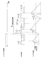
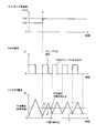
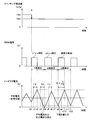
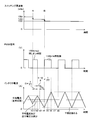
図3は、比較例に係るスイッチング周波数とPWM信号とインダクタ電流との関係を示すタイミングチャートであり、図4は、本発明の第1実施形態に係るスイッチング周波数とPWM信号とインダクタ電流との関係を示すタイミングチャートである。図3及び4夫々に示す3つのタイミング図では、何れも同一の時間軸を横軸にしてある。図3は本発明のような変更を行わない比較例(従来例)を示し、図4は本発明の第1実施形態に係る例を示している。両例とも、タイミングAにて、スイッチング周波数を150kHzから100kHzに切り替える。
図3に示す比較例(従来例)では、切替え直後のPWM信号におけるデューティ比は切替え前と同じであって、変更を行っていない。よって、切替え直後でのインダクタ電流は大きくなり、その平均値(破線aで表される)は、定常状態での平均値(実線bで表される)に比べて上昇する。この結果、出力電圧も大きく変動する。
これに対して、図4に示す本発明例では、スイッチング周波数の切替えに伴うインダクタ電流の変化を予測して、切替え直後のインダクタ電流の下限値が定常状態での下限値(破線cで表される)と一致するように、切替え直後のPWM信号の1周期におけるデューティ比を変更している。換言すれば、デューティ比を変更した周期とスイッチング周波数の切替え後の定常状態における各周期とでインダクタ電流の下限値を一致させる。
具体的には、切替え直後のPWM信号の1周期目にて、切替え前の各周期よりデューティ比が小さくなるように補正する。よって、切替え直後でのインダクタ電流はあまり大きくならず、その平均値(破線dで表される)の定常状態での平均値(実線eで表される)に対する上昇量は少ない。この結果、切替え後の出力電圧の変動が抑制される。なお、PWM信号の周波数の変更前及び変更後の夫々において、デューティ比を補正(変更)することと、オン時間を変更することとは、1対1に対応している。
以下、この切替え直後のPWM信号における波形の変更量、即ちスイッチング周波数を切り替えた直後における波形の変更(以下、単に変更とも言う)後のデューティ比及び変更後のオン時間の具体的な値について説明する。後述する導出過程を経て、変更後のデューティ比D′は下記(1)式で算出されることが導かれる。
D′={D(1-D)/2×(1/F1)+D(1+D)/2×(1/F2)}×F2
=D(1-D)/2×(F2/F1)+D(1+D)/2・・・・・・・・・(1)
但し、F1:切替え前のスイッチング周波数
F2:切替え後のスイッチング周波数
D:変更前のデューティ比
=D(1-D)/2×(F2/F1)+D(1+D)/2・・・・・・・・・(1)
但し、F1:切替え前のスイッチング周波数
F2:切替え後のスイッチング周波数
D:変更前のデューティ比
変更後のオン時間ON′は、D′×(1/F2)で求められるので、変更前のオン時間をONとした場合にD=ON×F1となる関係を上記(1)式における変形前の右辺に代入することにより、下記(2)式で算出される。
ON′={ON×F1×(1-ON×F1)}/(2×F1)
+{ON×F1×(1+ON×F1)}/(2×F2)・・・・・・・・(2)
+{ON×F1×(1+ON×F1)}/(2×F2)・・・・・・・・(2)
上記(1)式における変形後の右辺をX=F2/F1の一次関数と見た場合、この一次関数をグラフに描いたときの傾きがD(1-D)/2と常に正であって、X=1のときにD′=Dとなることが示される。よって、Xが1より小さい場合、即ちF2がF1より小さい場合は、D′をDより小さくすればよいことが示され、図4の切替え直後のPWM信号の1周期目にて、切替え前の各周期よりデューティ比が小さくなるように補正すればよいことが裏付けられる。
図5は、変更量の導出を説明するためのスイッチング周波数の切替え前後におけるスイッチング周波数とPWM信号とインダクタ電流との関係を示すタイミングチャートである。図の横軸は時間を表す。上記の(1)式の導出過程について、図5を参照して説明する。
スイッチング周波数の切替え前のインダクタ電流の上昇幅をIα、スイッチング周波数の切替え直後のインダクタ電流の上昇幅を(Iα/2)+Iβとした場合に、スイッチング周波数の切替え前後におけるスイッチング周波数、PWM信号及びインダクタ電流の関係を表すと図5のようになる。なお、図5において、Tβはスイッチング周波数の切替え直後のオン時間の一部を示している。
図5にて、スイッチング周波数をF1からF2に切り替えた直後に着目した場合、インダクタ電流の減少期間の傾きの絶対値は、インダクタ電流の増加期間の傾きのD/(1-D)倍とみなせる。即ち、インダクタ電流の増減が相殺する期間中におけるインダクタ電流の減少期間の長さが、インダクタ電流の増加期間の長さの(1-D)/D倍となるため、切替え後の周期1/F2は、下記(3)式にて求められる。
1/F2=(D/2)×(1/F1)+Tβ+{(1-D)/D}×Tβ
+{(1-D)/2}×(1/F2)・・・・・・・・・・・・・・・(3)
+{(1-D)/2}×(1/F2)・・・・・・・・・・・・・・・(3)
変更後のデューティ比D′は、オン時間÷周期、即ちオン時間×周波数で示されるので、D′は下記(4)式にて求められる。
D′={(D/2)×(1/F1)+Tβ}×F2・・・・・・・・・・・・・・(4)
上記(3)式を、Tβについて解くと、下記(5)式のようになる。
Tβ={D(1+D)/2}×(1/F2)-(D2 /2)×(1/F1)・・・(5)
上記(5)式を上記(4)式に代入することにより、変更後のデューティ比D′は以下のように求められて、上記(1)式が得られる。
D′=〔(D/2)×(1/F1)+{D(1+D)/2}×(1/F2)
-(D2 /2)×(1/F1)〕×F2
={D(1-D)/2×(1/F1)+D(1+D)/2×(1/F2)}×F2
=D(1-D)/2×(F2/F1)+D(1+D)/2
-(D2 /2)×(1/F1)〕×F2
={D(1-D)/2×(1/F1)+D(1+D)/2×(1/F2)}×F2
=D(1-D)/2×(F2/F1)+D(1+D)/2
次に、動作について説明する。図6は、電圧変換装置の動作手順を示すフローチャートである。図6に示す動作は、PWM制御の制御周期毎に実施され、ROM22に予め格納されている制御プログラムに従ってCPU21により実行される。
電圧変換装置の動作には、検出した出力電圧に基づくPWM信号におけるフィードバック制御であるオン時間算出処理(ステップS1)と、スイッチング周波数の切替えの要否を判定して、必要ならPWM信号における波形の変更量を算出して切替えを行う周波数切替え処理(ステップS2)とが含まれており、CPU21がこれらの処理を実行する。以下、このオン時間算出処理(ステップS1)及び周波数切替え処理(ステップS2)について詳述する。
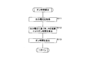
図7は、CPU21が行うオン時間算出処理の動作手順(ステップS1のサブルーチン)を示すフローチャートである。
CPU21は、負荷4に出力された出力電圧をA/D変換回路27で変換したデジタルの電圧値を取得する(ステップS11)。次いで、CPU21は、取得した出力電圧の電圧値(Vo)に基づいて、出力電圧が目標の電圧値(Vref)になるようにPID演算を行って、オン時間を算出する(ステップS12)。CPU21は、算出したオン時間をPWM回路25に送出して(ステップS13)、処理を終了する。送出されたオン時間に従ってPWM回路25にてPWM信号が生成される。
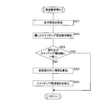
図8は、CPU21が行う周波数切替え処理の動作手順(ステップS2のサブルーチン)を示すフローチャートである。
図8の処理が呼び出された場合、CPU21は、負荷4に出力された出力電流をA/D変換回路26で変換したデジタルの電流値を取得する(ステップS21)。CPU21は、取得した出力電流の電流値に適したスイッチング周波数を特定する(ステップS22)。具体的には、CPU21は、取得した電流値が20A以上である場合にはスイッチング周波数を150kHzと特定し、取得した電流値が20A未満である場合にはスイッチング周波数を100kHzと特定する。
CPU21は、特定したスイッチング周波数が現時点のスイッチング周波数に一致するか否かを判定する(ステップS23)。一致する場合に(S23:YES)、CPU21は処理を終了する。
一方、一致しない場合には(S23:NO)、CPU21は、前述した(2)式に従って、変更前のオン時間と、現時点のスイッチング周波数(変更前のスイッチング周波数)と、特定したスイッチング周波数(変更後のスイッチング周波数)とを用いて、変更後のオン時間を算出する(ステップS24)。そして、CPU21は、現時点のスイッチング周波数を、特定したスイッチング周波数に切り替えて(ステップS25)、処理を終了する。PWM信号のスイッチング周波数の切替え直後の1周期目におけるオン時間は、ステップS24で算出されたオン時間である。
上述した第1実施形態では、バッテリ3からの電圧の変換効率を高めるためにスイッチング素子11、12に対するスイッチング周波数を低下させるべく切り替える場合、切替え直後のPWM信号の波形の特性(オン時間又はデューティ比)を変更するようにしたので、切替えに起因する切替え後のインダクタ電流の平均値の上昇を抑えることができ、その結果、出力電圧の変動を抑制することができて、定電圧を安定して負荷4に出力することが可能である。
(変形例1)
第1実施形態が、スイッチング周波数を高い周波数から低い周波数に低下させるべく切り替える形態であるのに対し、変形例1は、スイッチング周波数を低い周波数から高い周波数に上昇させるべく切り替える形態である。以下、本発明の第1実施形態の変形例1について説明する。変形例1に係る電圧変換装置の構成は、前述した第1実施形態に係る電圧変換装置の構成(図1及び図2)と同様である。
第1実施形態が、スイッチング周波数を高い周波数から低い周波数に低下させるべく切り替える形態であるのに対し、変形例1は、スイッチング周波数を低い周波数から高い周波数に上昇させるべく切り替える形態である。以下、本発明の第1実施形態の変形例1について説明する。変形例1に係る電圧変換装置の構成は、前述した第1実施形態に係る電圧変換装置の構成(図1及び図2)と同様である。
図9は、変形例1に係るスイッチング周波数とPWM信号とインダクタ電流との関係を示すタイミングチャートである。図中の3つのタイミング図では、何れも同一の時間軸を横軸にしてある。変形例1では、タイミングAにてスイッチング周波数を100kHzから150kHzに切り替える。図9に示す例では、スイッチング周波数の切替えに伴うインダクタ電流の変化を予測して、切替え直後のインダクタ電流の下限値が定常状態での下限値(破線cで表される)と一致するように、切替え直後のPWM信号の1周期におけるデューティ比を変更している。換言すれば、デューティ比を変更した周期とスイッチング周波数の切替え後の定常状態における各周期とでインダクタ電流の下限値を一致させる。
具体的には、切替え直後のPWM信号の1周期目にて、切替え前の各周期よりデューティ比が大きくなるように補正する。前述の(1)式における変形後の右辺をX=F2/F1の一次関数と見た場合、この一次関数をグラフに描いたときの傾きがD(1-D)/2と常に正であって、X=1のときにD′=Dとなるから、Xが1より大きい場合、即ちF2がF1より大きい場合は、D′をDより大きくすればよいことが示される。このようにデューティ比を補正した場合、切替え直後でのインダクタ電流はあまり小さくならず、その平均値(破線dで表される)の定常状態での平均値(実線eで表される)に対する下降量が抑えられる。この結果、切替え後の出力電圧の変動が抑制される。
なお、変形例1にあっては、変更前のデューティ比Dが1に近い場合、(1)式によって算出されるD'が1を超えるときがあり得るが、そのときにはD'を限りなく1に近い数値にすればよい。
(第2実施形態)
以下、本発明の第2実施形態について説明する。なお、第2実施形態に係る電圧変換装置の構成は、前述した第1実施形態に係る電圧変換装置の構成(図1及び図2)と同様である。
以下、本発明の第2実施形態について説明する。なお、第2実施形態に係る電圧変換装置の構成は、前述した第1実施形態に係る電圧変換装置の構成(図1及び図2)と同様である。
前述した第1実施形態では、スイッチング周波数の切替え直後のPWM信号の1周期におけるオン時間を変更したが、第2実施形態では、スイッチング周波数の切替え直前のPWM信号の1周期におけるオン時間を変更する。この第2実施形態は、スイッチング周波数を切替えた直後からPWM制御を特段の補正無しで行いたい場合に好適である。
図10は、本発明の第2実施形態に係るスイッチング周波数とPWM信号とインダクタ電流との関係を示すタイミングチャートである。図中の3つのタイミング図では、何れも同一の時間軸を横軸にしてある。第1実施形態と同様に、タイミングAにてスイッチング周波数を150kHzから100kHzに切り替える。図10に示す例では、スイッチング周波数の切替えに伴うインダクタ電流の変化を予測して、切替え時のインダクタ電流の下限値が定常状態での下限値(破線cで表される)と一致するように、切替え直前のPWM信号の1周期におけるデューティ比を変更している。換言すれば、デューティ比を変更した周期とスイッチング周波数の切替え後の定常状態における各周期とでインダクタ電流の下限値を一致させる。
具体的には、切替え直前のPWM信号の1周期にて、その前の周期より(即ち切替え後の各周期より)デューティ比が小さくなるように補正する。よって、切替え直前の1周期におけるインダクタ電流が小さくなり、その平均値(破線dで表される)は定常状態での平均値(実線eで表される)に対して適当に下降する。この結果、切替え後のインダクタ電流の平均値の上昇が抑えられて、切替え後の出力電圧の変動が抑制される。
以下、この切替え直前のPWM信号における波形の変更量、即ちスイッチング周波数を切り替える直前における波形の変更後のデューティ比及び変更後のオン時間の具体的な値について説明する。後述する導出過程を経て、変更後のデューティ比D′は下記(6)式で算出されることが導かれる。
D′={D(3-D)/2×(1/F1)+D(D-1)/2×(1/F2)}×F1
=D(3-D)/2+D(D-1)/2×(F1/F2)・・・・・・・・・(6)
但し、F1:切替え前のスイッチング周波数
F2:切替え後のスイッチング周波数
D:変更前のデューティ比
=D(3-D)/2+D(D-1)/2×(F1/F2)・・・・・・・・・(6)
但し、F1:切替え前のスイッチング周波数
F2:切替え後のスイッチング周波数
D:変更前のデューティ比
変更後のオン時間ON′は、D′×(1/F1)で求められるので、変更前のオン時間をONとした場合にD=ON×F1となる関係を上記(6)式における変形前の右辺に代入することにより、下記(7)式で算出される。
ON′={ON×F1×(3-ON×F1)}/(2×F1)
+{ON×F1×(ON×F1-1)}/(2×F2)・・・・・・・・(7)
+{ON×F1×(ON×F1-1)}/(2×F2)・・・・・・・・(7)
上記(6)式における変形後の右辺をY=F1/F2の一次関数と見た場合、この一次関数をグラフに描いたときの傾きがD(D-1)/2と常に負であって、Y=1のときにD′=Dとなることが示される。よって、Yが1より大きい場合、即ちF2がF1より小さい場合は、D′をDより小さくすればよいことが示され、図10の切替え直前のPWM信号の1周期にて、その前の周期より(即ち切替え後の各周期より)デューティ比が小さくなるように補正すればよいことが裏付けられる。
図11は、変更量の導出を説明するためのスイッチング周波数の切替え前後におけるスイッチング周波数とPWM信号とインダクタ電流との関係を示すタイミングチャートである。図の横軸は時間を表す。上記の算出式の導出過程について、図11を参照して説明する。
図5の場合と同様に、スイッチング周波数の切替え前のインダクタ電流の上昇幅をIα、スイッチング周波数の切替え直前のインダクタ電流の上昇幅を(Iα/2)+Iβとした場合に、スイッチング周波数の切替え前後におけるスイッチング周波数、PWM信号及びインダクタ電流の関係を表すと図11のようになる。Tβはスイッチング周波数の切替え直前のオン時間の一部を示している。
図11にて、スイッチング周波数をF1からF2に切り替える直前に着目した場合、図5の場合と同様に、インダクタ電流の増減が相殺する期間中におけるインダクタ電流の減少期間の長さが、インダクタ電流の増加期間の長さの(1-D)/D倍となるため、切替え直前の周期1/F1は、下記(8)式にて求められる。
1/F1=(D/2)×(1/F1)+Tβ+{(1-D)/D}×Tβ
+{(1-D)/2}×(1/F2)・・・・・・・・・・・・・・・(8)
+{(1-D)/2}×(1/F2)・・・・・・・・・・・・・・・(8)
上述したように、変更後のデューティ比D′はオン時間×周波数で示されるので、D′は下記(4)式(再掲)にて求められる。
D′={(D/2)×(1/F1)+Tβ}×F2・・・・・・・・・・・・・・(4)
上記(8)式を、Tβについて解くと、下記(9)式のようになる。
Tβ={D(2-D)/2}×(1/F1)+{D(D-1)/2}×(1/F2)・・・・・・・・・・・・・・・・・・・・・・・・・・・・・・・・・・・・・・・(9)
(9)式を上記(4)式に代入することにより、変更後のデューティ比D′は以下のように求められて、上記(6)式が得られる。
D′=〔(D/2)×(1/F1)+{D(2-D)/2}×(1/F1)
+{D(D-1)/2}×(1/F2)〕×F1
={D(3-D)/2×(1/F1)+D(D-1)/2×(1/F2)}×F1
+{D(D-1)/2}×(1/F2)〕×F1
={D(3-D)/2×(1/F1)+D(D-1)/2×(1/F2)}×F1
次に、動作について説明する。電圧変換装置の動作手順を示すフローチャート、及びCPU21が行うオン時間算出処理の動作手順(ステップS1のサブルーチン)を示すフローチャートは、第1実施形態における図6及び図7に示すものと同様であるため、図示及びその説明を省略する。
図12は、CPU21が行う周波数切替え処理の動作手順(ステップS2のサブルーチン)を示すフローチャートである。図中の切替フラグは、スイッチング周波数を切り替える周期であるか否かを示すフラグであり、初期値を0にしてRAM23に記憶される。図12に示すステップS31からS34までの処理は、第1実施形態における図8に示すステップS21からS24までの処理と同様であるため、その説明を簡略化する。
図12の処理が呼び出された場合、CPU21は、切替フラグが1にセットされているか否かを判定する(ステップS30)。切替フラグが1にセットされていない場合(S30:NO)、CPU21は、負荷4に出力された出力電流を取得し(ステップS31)、取得した出力電流に適したスイッチング周波数を特定する(ステップS32)。
次いで、CPU21は、特定したスイッチング周波数が現時点のスイッチング周波数に一致するか否かを判定し(ステップS33)、一致する場合(S33:YES)、処理を終了する。
一方、一致しない場合には(S33:NO)、CPU21は、前述した(7)式に従って変更後のオン時間を算出し(ステップS34)、切替フラグを1にセットして(ステップS35)処理を終了する。
ステップS30で切替フラグが1にセットされている場合(S30:YES)、CPU21は、切替フラグを0にクリアした(ステップS36)後、現時点のスイッチング周波数を、特定したスイッチング周波数に切り替えて(ステップS37)処理を終了する。
上述した第2実施形態では、バッテリ3からの電圧の変換効率を高めるためにスイッチング素子11、12に対するスイッチング周波数を低下させるべく切り替える場合、切替え直前のPWM信号の波形の特性(オン時間又はデューティ比)を変更するようにしたので、切替えに起因する切替え後のインダクタ電流の平均値の上昇を抑えることができ、その結果、出力電圧の変動を抑制することができて、定電圧を安定して負荷4に出力することが可能である。
なお、第2実施形態にあっては、変更前のデューティ比Dが0に近い場合、(6)式によって算出されるD'が0を下回るときがあり得るが、そのときにはD'を限りなく0に近い数値にすればよい。
(変形例2)
第2実施形態が、スイッチング周波数を高い周波数から低い周波数に低下させるべく切り替える形態であるのに対し、変形例2は、スイッチング周波数を低い周波数から高い周波数に上昇させるべく切り替える形態である。以下、本発明の第2実施形態の変形例2について説明する。変形例2に係る電圧変換装置の構成は、前述した第1実施形態に係る電圧変換装置の構成(図1及び図2)と同様である。
第2実施形態が、スイッチング周波数を高い周波数から低い周波数に低下させるべく切り替える形態であるのに対し、変形例2は、スイッチング周波数を低い周波数から高い周波数に上昇させるべく切り替える形態である。以下、本発明の第2実施形態の変形例2について説明する。変形例2に係る電圧変換装置の構成は、前述した第1実施形態に係る電圧変換装置の構成(図1及び図2)と同様である。
図13は、変形例2に係るスイッチング周波数とPWM信号とインダクタ電流との関係を示すタイミングチャートである。図中の3つのタイミング図では、何れも同一の時間軸を横軸にしてある。変形例2では、タイミングAにてスイッチング周波数を100kHzから150kHzに切り替える。図13に示す例では、スイッチング周波数の切替えに伴うインダクタ電流の変化を予測して、切替え時のインダクタ電流の下限値が定常状態での下限値(破線cで表される)と一致するように、切替え直前のPWM信号の1周期におけるデューティ比を変更している。換言すれば、デューティ比を変更した周期とスイッチング周波数の切替え後の定常状態における各周期とでインダクタ電流の下限値を一致させる。
具体的には、切替え直前のPWM信号の1周期にて、その前の周期より(即ち切替え後の各周期より)デューティ比が大きくなるように補正する。前述の(6)式における変形後の右辺をY=F1/F2の一次関数と見た場合、この一次関数をグラフに描いたときの傾きがD(D-1)/2と常に負であって、Y=1のときにD′=Dとなるから、Yが1より小さい場合、即ちF2がF1より大きい場合は、D′をDより大きくすればよいことが示される。このようにデューティ比を補正した場合、切替え直前でのインダクタ電流が大きくなり、その平均値(破線dで表される)は定常状態での平均値(実線eで表される)に対して適当に上昇する。この結果、切替え後のインダクタ電流の平均値の下降が抑えられて、出力電圧の変動が抑制される。
(第3実施形態)
以下、本発明の第3実施形態について説明する。なお、第3実施形態に係る電圧変換装置の構成は、前述した第1実施形態に係る電圧変換装置の構成(図1及び図2)と同様である。
以下、本発明の第3実施形態について説明する。なお、第3実施形態に係る電圧変換装置の構成は、前述した第1実施形態に係る電圧変換装置の構成(図1及び図2)と同様である。
前述した第1及び第2実施形態夫々では、スイッチング周波数の切替え直後及び切替え直前のPWM信号の1周期におけるオン時間のみを変更したが、第3実施形態では、スイッチング周波数の切替え直後のPWM信号の複数周期におけるオン時間を変更する。この第3実施形態は、出力電圧に基づくフィードバック制御をPWM信号の1周期ごとに行わない場合に好適である。
図14は、本発明の第3実施形態に係るスイッチング周波数とPWM信号とインダクタ電流との関係を示すタイミングチャートである。図中の3つのタイミング図では、何れも同一の時間軸を横軸にしてある。第1実施形態と同様に、タイミングAにてスイッチング周波数を150kHzから100kHzに切り替える。図14に示す例では、スイッチング周波数の切替え直後の2周期にわたってオン時間を変更している。即ち、スイッチング周波数の切替え直後の1周期目では、インダクタ電流の上限値を定常状態における上限値に一致させるように、オン時間をx1μsだけ変更し、2周期目では、インダクタ電流の下限値を定常状態における下限値に一致させるように、オン時間をx2μsだけ変更し、3周期目以降からは、通常の制御を行っている。換言すれば、デューティ比を変更した1周期目及び2周期目夫々とスイッチング周波数の切替え後の定常状態における各周期とでインダクタ電流の上限値及び下限値を一致させる。
具体的なオン時間の変更量について、図5を参照しつつ図14を用いて説明する。図14にて、スイッチング周波数を切り替える時刻をt0とし、その直後にインダクタ電流が平均電流と一致する時刻をt1とする。以後、インダクタ電流が順次平均電流と一致する時刻をt3,t5,t7,t9,t11とし、順次極大値及び極小値となる時刻をt2,t4,t6,t8,t10,t12とする。
時刻t1からt2までの時間は、図5におけるTβに相当し、時刻t8からt10までの時間は、図5におけるD×1/F2に相当する。本第3実施形態では、時刻t2及びt10におけるインダクタ電流が等しくなるように制御するため、以下の(10)式が成立する。また、上述したように、変更後のデューティ比D′はオン時間×周波数で示されるので、D′は下記(4)式(再掲)にて求められる。
Tβ=(D/2)×(1/F2)・・・・・・・・・・・・・・・・・・・・・(10)
D′={(D/2)×(1/F1)+Tβ}×F2・・・・・・・・・・・・・・(4)
D′={(D/2)×(1/F1)+Tβ}×F2・・・・・・・・・・・・・・(4)
(10)式を(4)式に代入することにより、スイッチング周波数の切替え後の1周期目(時刻t0からt4まで)におけるデューティ比D′が、以下の(11)式のとおり求められる。この(11)式で最後に変形された右辺の第2項に周期(1/F2)を乗算したものが、時刻t0からt2までのPWM信号のオン時間の補正量(上記のx1μsに相当)である。スイッチング周波数を150kHzから100kHzに切り替える場合、即ちF2/F1が1より小さい場合、切替え直後のデューティ比が切替え前より小さくなるように補正される。この場合、x1は負の数となり、切替え直後のPWM信号のオン時間が、切替え後の定常状態におけるオン時間より短くなるように補正される。
D′={(D/2)×(1/F1)+(D/2)×(1/F2)}×F2
=(D/2)×(F2/F1+1)
=D-(D/2)×(1-F2/F1)・・・・・・・・・・・・・・・・(11)
=(D/2)×(F2/F1+1)
=D-(D/2)×(1-F2/F1)・・・・・・・・・・・・・・・・(11)
次に、スイッチング周波数の切替え後の2周期目(時刻t4からt8まで)におけるPWM信号の補正量について説明する。スイッチング周波数の切替え後の1周期目では、(11)式で示されるようにデューティ比D′をDより小さくして補正したので、時刻t2からt4までの時間が、周波数F2での通常の制御における時刻t10からt12までの時間よりも長くなり、その分だけインダクタ電流が余分に減少する。
1周期目における時刻t3からt4までの時間をT3とすると、時刻t0からt1までの時間は、図5の場合と同様に(D/2)×(1/F1)である。また、時刻t1からt3までの時間は、時刻t9からt11までの時間と同じく1周期の半分に相当する(1/2)×(1/F2)である。時刻t0からt4までの時間は1/F2であるから、T3は下記(12)式にて求められる。
T3=(1/2)×(1/F2)-(D/2)×(1/F1)・・・・・・・・(12)
次に、2周期目における時刻t5からt6までの時間をTγとする。上述したように、インダクタ電流の増減が相殺する期間中におけるインダクタ電流の減少期間の長さが、インダクタ電流の増加期間の長さの(1-D)/D倍とみなせるから、2周期目における時刻t4からt5までの時間はT3のD/(1-D)倍となり、時刻t6からt7までの時間はTγの(1-D)/D倍となる。また、時刻t7からt8までの時間は、{(1-D)/2}×(1/F2)であるから、2周期目全体の時間について下記(13)式が成立する。
1/F2=T3×D/(1-D)+Tγ+{(1-D)/D}×Tγ
+{(1-D)/2}×(1/F2)・・・・・・・・・・・・・・(13)
+{(1-D)/2}×(1/F2)・・・・・・・・・・・・・・(13)
変更後のデューティ比は、時刻t4からt6までのオン時間÷周期、即ちオン時間×周波数で示されるので、変更後のデューティ比D”は下記(14)式にて求められる。
D”={T3×D/(1-D)+Tγ}×F2・・・・・・・・・・・・・・・(14)
上記(13)式を、Tγについて解くと、下記(15)式のようになる。
Tγ={D(1+D)/2}×(1/F2)-T3×D2 /(1-D)・・・・(15)
上記(12)式と、(12)式を上記(15)式に代入した式とを(14)式に代入することにより、変更後のデューティ比D”は以下の(16)式のようになる。但し、式の変形の途中結果については記載を省略する。この(16)式で最後に変形された右辺の第2項に周期(1/F2)を乗算したものが、時刻t4からt6までのPWM信号の補正量(上記のx2μsに相当)である。スイッチング周波数を150kHzから100kHzに切り替える場合、即ちF2/F1が1より小さい場合、切替え後の2周期目におけるデューティ比が切替え前の各周期より大きくなるように補正される。この場合、x2は正の数となり、切替え後の2周期目のPWM信号のオン時間が、切替え後の定常状態における各周期のオン時間より長くなるように補正される。
D”={-(D2 /2)×(1/F1)
+(D/2)×(2+D)×(1/F2)}×F2
=D+(D2 /2)×(1-F2/F1)・・・・・・・・・・・・・・・(16)
+(D/2)×(2+D)×(1/F2)}×F2
=D+(D2 /2)×(1-F2/F1)・・・・・・・・・・・・・・・(16)
上記(11)式(又は(16)式)における変形後の右辺をX=F2/F1の一次関数と見た場合、この一次関数をグラフに描いたときの傾きがD/2(又は-(D2 /2)と常に正(又は負)であって、X=1のときにD′=D(又はD”=D)となることが示される。よって、Xが1より小さい場合、即ちF2がF1より小さい場合は、D′をDより小さく(又はD”をDより大きく)すればよいことが示され、図14の切替え直後のPWM信号の1周期目(又は2周期目)にて、切替え前の各周期よりデューティ比が小さく(又は大きく)なるように補正すればよいことが裏付けられる。
また、(11)式(又は(16)式)にてX=F2/F1が1より大きい場合、即ちF2がF1より大きい場合は、D′をDより大きく(又はD”をDより小さく)すればよいことが示される。つまり、切替え直後のPWM信号の1周期目(又は2周期目)にて、切替え前の各周期よりデューティ比が大きく(又は小さく)なるように補正すればよい。
以上のように、第3実施形態では、出力電圧の変動が、増加する方向ではなくて減少する方向となるため、スイッチング周波数を切り替える場合、仕様に示された上限電圧を超える虞がなくなる。
なお、スイッチング周波数の切替え直後の3周期以上にわたってオン時間を変更する場合は、スイッチング周波数を切り替えた後のインダクタ電流の推移を想定し、その想定結果からインダクタ電流の上限値または下限値が定常状態での上限値または下限値に一致するように、切替え前のスイッチング周波数、切替え後のスイッチング周波数、及び変更前のデューティ比を用いて、前述した第3実施形態と同様に算出すれば良い。
また、第3実施形態にあっては、X=F2/F1が1より大きく、且つ変更前のデューティ比Dが1に近い場合、(11)式によって算出されるD'が1を超えるときがあり得るが、そのときにはD'を限りなく1に近い数値にし、例えばD"をDにすればよい。
(第4実施形態)
以下、本発明の第4実施形態について説明する。なお、第4実施形態に係る電圧変換装置の構成は、前述した第1実施形態に係る電圧変換装置の構成(図1及び図2)と同様である。前述した第3実施形態が、スイッチング周波数の切替え直後の2周期にわたってPWM信号のオン信号の長さを補正する形態であるのに対し、第4実施形態は、スイッチング周波数の切替え直前の2周期にわたってPWM信号のオン信号の長さを補正する形態である。
以下、本発明の第4実施形態について説明する。なお、第4実施形態に係る電圧変換装置の構成は、前述した第1実施形態に係る電圧変換装置の構成(図1及び図2)と同様である。前述した第3実施形態が、スイッチング周波数の切替え直後の2周期にわたってPWM信号のオン信号の長さを補正する形態であるのに対し、第4実施形態は、スイッチング周波数の切替え直前の2周期にわたってPWM信号のオン信号の長さを補正する形態である。
図15は、本発明の第4実施形態に係るスイッチング周波数とPWM信号とインダクタ電流との関係を示すタイミングチャートである。図中の3つのタイミング図では、何れも同一の時間軸を横軸にしてある。第1実施形態と同様に、タイミングAにてスイッチング周波数を150kHzから100kHzに切り替える。図15に示す例では、切替え直前のPWM信号の2周期にわたってオン時間を変更している。即ち、スイッチング周波数の切替え直前の2周期のうち、1周期目(時刻t0からt4まで)では、インダクタ電流の上限値を定常状態における上限値に一致させるように、オン時間をy1μsだけ変更し、2周期目(時刻t4からt8まで)では、インダクタ電流の下限値を定常状態における下限値に一致させるように、オン時間をy2μsだけ変更し、切替え直後からは、通常の制御を行っている。換言すれば、デューティ比を変更した1周期目及び2周期目夫々とスイッチング周波数の切替え後の定常状態における各周期とでインダクタ電流の上限値及び下限値を一致させる。
具体的なオン時間の変更量について、図5を参照しつつ図15を用いて説明する。図15にて、スイッチング周波数を切り替える時刻の2周期前の時刻をt0とし、その直後にインダクタ電流が平均電流と一致する時刻をt1とする。以後、インダクタ電流が順次平均電流と一致する時刻をt3,t5,t7,t9,t11とし、順次極大値及び極小値となる時刻をt2,t4,t6,t8,t10,t12とする。スイッチング周波数を切り替える時刻はt8である。
時刻t1からt2までの時間は、図5におけるTβに相当し、時刻t8からt10までの時間は、図5におけるD×1/F2に相当する。本第4実施形態では、時刻t2及びt10におけるインダクタ電流が等しくなるように制御するため、以下の(10)式(再掲)が成立する。また、上述したように、変更後のデューティ比D′はオン時間×周波数で示されるので、D′は下記(17)式にて求められる。
Tβ=(D/2)×(1/F2)・・・・・・・・・・・・・・・・・・・・・(10)
D′={(D/2)×(1/F1)+Tβ}×F1・・・・・・・・・・・・・(17)
D′={(D/2)×(1/F1)+Tβ}×F1・・・・・・・・・・・・・(17)
(10)式を(17)式に代入することにより、スイッチング周波数の切替え直前の2周期のうち1周期目におけるデューティ比D′が、以下の(18)式のとおり求められる。この(18)式で最後に変形された右辺の第2項に周期(1/F1)を乗算したものが、時刻t0からt2までのPWM信号の補正量(上記のy1μsに相当)である。スイッチング周波数を150kHzから100kHzに切り替える場合、即ちF1/F2が1より大きい場合、切替え直前の2周期のうち1周期目のデューティ比が、その前の周期より(即ち切替え後の各周期より)大きくなるように補正される。この場合、y1は正の数となり、切替え直前の2周期のうち1周期目のPWM信号のオン時間が、切替え後の定常状態におけるオン時間より長くなるように補正される。
D′={(D/2)×(1/F1)+(D/2)×(1/F2)}×F1
=(D/2)×(1+F1/F2)
=D-(D/2)×(1-F1/F2)・・・・・・・・・・・・・・・・(18)
=(D/2)×(1+F1/F2)
=D-(D/2)×(1-F1/F2)・・・・・・・・・・・・・・・・(18)
次に、スイッチング周波数の切替え直前の2周期のうち、2周期目におけるPWM信号の補正量について説明する。1周期目における時刻t3からt4までの時間をT3(図示せず:図14参照)とすると、時刻t0からt1までの時間は、図5の場合と同様に(D/2)×(1/F1)である。また、時刻t1からt3までの時間は、時刻t9からt11までの時間と同じく1周期の半分に相当する(1/2)×(1/F2)である。時刻t0からt4までの時間は1/F1であるから、T3は下記(19)式にて求められる。
T3=(1/F1)-(1/2)×(1/F2)-(D/2)×(1/F1)
=(2-D)/2×(1/F1)-(1/2)×(1/F2)・・・・・・(19)
=(2-D)/2×(1/F1)-(1/2)×(1/F2)・・・・・・(19)
次に、2周期目における時刻t5からt6までの時間をTγとする。上述したように、インダクタ電流の増減が相殺する期間中におけるインダクタ電流の減少期間の長さが、インダクタ電流の増加期間の長さの(1-D)/D倍とみなせるから、2周期目における時刻t4からt5までの時間はT3のD/(1-D)倍となり、時刻t6からt7までの時間はTγの(1-D)/D倍となる。また、時刻t7からt8までの時間は、{(1-D)/2}×(1/F1)であるから、2周期目全体の時間について下記(20)式が成立する。
1/F1=T3×D/(1-D)+Tγ+{(1-D)/D}×Tγ
+{(1-D)/2}×(1/F1)・・・・・・・・・・・・・・(20)
+{(1-D)/2}×(1/F1)・・・・・・・・・・・・・・(20)
変更後のデューティ比は、時刻t4からt6までのオン時間÷周期、即ちオン時間×周波数で示されるので、変更後のデューティ比D”は下記(21)式にて求められる。
D”={T3×D/(1-D)+Tγ}×F1・・・・・・・・・・・・・・・(21)
上記(20)式を、Tγについて解くと、下記(22)式のようになる。
Tγ={D(1+D)/2}×(1/F1)-T3×D2 /(1-D)・・・・(22)
上記(19)式と、(19)式を上記(22)式に代入した式とを(21)式に代入することにより、変更後のデューティ比D”は以下の(23)式のようになる。但し、式の変形の途中結果については記載を省略する。この(23)式で最後に変形された右辺の第2項に周期(1/F1)を乗算したものが、時刻t4からt6までのPWM信号の補正量(上記のy2μsに相当)である。スイッチング周波数を150kHzから100kHzに切り替える場合、即ちF1/F2がF1より大きい場合、切替え直前の2周期のうち1周期目のデューティ比が、その前の周期より(即ち切替え後の各周期より)小さくなるように補正される。この場合、y2は負の数となり、切替え直前の2周期のうち2周期目のPWM信号のオン時間が、切替え後の定常状態におけるオン時間より短くなるように補正される。
D”={3×D/2×(1/F1)}×F1-{(D/2)×(1/F2)}×F1
=D+(D/2)×(1-F1/F2)・・・・・・・・・・・・・・・・(23)
=D+(D/2)×(1-F1/F2)・・・・・・・・・・・・・・・・(23)
上記(18)式(又は(23)式)における変形後の右辺をY=F1/F2の一次関数と見た場合、この一次関数をグラフに描いたときの傾きがD/2(又は-D/2)と常に正(又は負)であって、Y=1のときにD′=D(又はD”=D)となることが示される。よって、Yが1より大きい場合、即ちF2がF1より小さい場合は、D′をDより大きく(又はD”をDより小さく)すればよいことが示され、図15の切替え直前の2周期のうち、1周期目(又は2周期目)にて、その前の周期、即ち切替え後の各周期よりデューティ比が大きく(又は小さく)なるように補正すればよいことが裏付けられる。
また、(18)式(又は(23)式)にてY=F1/F2が1より小さい場合、即ちF2がF1より大きい場合は、D′をDより小さく(又はD”をDより大きく)すればよいことが示される。つまり、切替え直前の2周期のうち、1周期目(又は2周期目)にて、切替え後の各周期よりデューティ比が小さく(又は大きく)なるように補正すればよい。
以上のように、第4実施形態では、出力電圧の変動が、増加する方向ではなくて減少する方向となるため、スイッチング周波数を切り替える場合、仕様に示された上限電圧を超える虞がなくなる。
なお、第4実施形態にあっては、Y=F1/F2が1より大きく、且つ変更前のデューティ比Dが1に近い場合、(18)式によって算出されるD'が1を超えるときがあり得るが、そのときにはD'を限りなく1に近い数値にし、例えばD"をDにすればよい。
(第5実施形態)
以下、本発明の第5実施形態について説明する。なお、第5実施形態に係る電圧変換装置の構成は、前述した第1実施形態に係る電圧変換装置の構成(図1及び図2)と同様である。
以下、本発明の第5実施形態について説明する。なお、第5実施形態に係る電圧変換装置の構成は、前述した第1実施形態に係る電圧変換装置の構成(図1及び図2)と同様である。
前述した第1実施形態では、スイッチング周波数の切替え直後のPWM信号の1周期におけるオン時間を変更したが、第5実施形態では、スイッチング周波数の切替え直後のPWM信号の1周期における周波数を変更する。この第5実施形態は、スイッチング周波数の切替え直前のPWM信号の1周期における周波数を変更する形態とみなすこともできる。
図16は、本発明の第5実施形態に係るスイッチング周波数とPWM信号とインダクタ電流との関係を示すタイミングチャートである。図中の3つのタイミング図では、何れも同一の時間軸を横軸にしてある。第1実施形態と同様に、タイミングA(又はタイミングB)にてスイッチング周波数を切り替える。この際、図16に示す例では、スイッチング周波数の切替え直後(又は切替え直前)の1周期だけはオン時間を変更することなくPWM信号の周波数を例えば120kHzとして、2周期目以降(又は切替え後)はPWM信号の周波数を100kHzとする。
このように、第5実施形態では、スイッチング周波数の切替え直後(又は切替え直前)のインダクタ電流の下限値を定常状態での下限値に揃えるために、スイッチング周波数の切替え直後(又は切替え直前)に、PWM信号のオン時間を変更するのではなく、PWM信号の周波数を変更している。換言すれば、PWM信号の周波数を変更した周期とスイッチング周波数の切替え後の定常状態における各周期とでインダクタ電流の下限値を一致させる。
具体的な周波数の変更量について、図5を参照しつつ図16を用いて説明する。図16にて、スイッチング周波数を切り替える時刻をt0(又はt4)とし、時刻t0直後にインダクタ電流が平均電流と一致する時刻をt1とする。以後、インダクタ電流が順次平均電流と一致する時刻をt3,t5,t7とし、順次極大値及び極小値となる時刻をt2,t4,t6,t8とする。
時刻t0からt2までの時間は、図5におけるスイッチング周波数の切替え前のD×(1/F1)に相当する。また、時刻t2からt3までの時間は、図5におけるスイッチング周波数の切替え前の(1-D)×(1/F1)の半分に相当する。時刻t0からt4までの時間は1/F2である。よって、時刻t3からt4までの時間をT3とすると、T3は下記(24)式にて求められる。
T3=(1/F2)-D×(1/F1)
-{(1-D)/2}×(1/F1)・・・・・・・・・・・・・・・・(24)
但し、F1:切替え前のスイッチング周波数
F2:切替え直後(又は切替え直前)のスイッチング周波数
D:デューティ比
-{(1-D)/2}×(1/F1)・・・・・・・・・・・・・・・・(24)
但し、F1:切替え前のスイッチング周波数
F2:切替え直後(又は切替え直前)のスイッチング周波数
D:デューティ比
本実施の形態5では、時刻t4及びt8におけるインダクタ電流が等しくなるように制御するため、時刻t4におけるインダクタ電流の谷の深さ(平均電流と極小値との差分)は、時刻t8におけるインダクタ電流の谷の深さと同一である。これらの谷の深さは時刻t6におけるインダクタ電流の山の高さ(平均電流と極大値との差分)と同一である。
ここで、切替え後の2周期目以降(又は切替え後)のスイッチング周波数をF3とすると、時刻t2におけるインダクタ電流の山の高さに対する時刻t6における山の高さの比は、F3に対するF1の比に等しいから、時刻t2からt3までの時間に対するT3の比がF3に対するF1の比に等しくなり、以下の(25)式が成立する。
{(1-D)/2}×(1/F1)/T3=F3/F1・・・・・・・・・・・(25)
(25)式に(24)式を代入してF2について解くと、以下の(26)式のようになる。このF2を、スイッチング周波数の切替え直後(又は切替え直前)の1周期のスイッチング周波数とすればよい。
F2=2×F1×F3/{(1-D)×F1+(1+D)×F3}・・・・・・(26)
(第6実施形態)
以下、本発明の第6実施形態について説明する。なお、第6実施形態に係る電圧変換装置の構成は、前述した第1実施形態に係る電圧変換装置の構成(図1及び図2)と同様である。
以下、本発明の第6実施形態について説明する。なお、第6実施形態に係る電圧変換装置の構成は、前述した第1実施形態に係る電圧変換装置の構成(図1及び図2)と同様である。
前述した第1及び第2実施形態夫々では、スイッチング周波数の切替え直後及び直前のPWM信号の1周期におけるオン時間のみを変更したが、第6実施形態では、スイッチング周波数の切替え直前及び直後夫々のPWM信号の1周期におけるオン時間を変更する。この第6実施形態は、出力電圧に基づくフィードバック制御をPWM信号の1周期ごとに行わない場合に好適である。
図17は、本発明の第6実施形態に係るスイッチング周波数とPWM信号とインダクタ電流との関係を示すタイミングチャートである。図中の3つのタイミング図では、何れも同一の時間軸を横軸にしてある。第4実施形態と同様に、タイミングAにてスイッチング周波数を150kHzから100kHzに切り替える。図17に示す例では、スイッチング周波数の切替えに伴うインダクタ電流の変化を予測して、切替え直後の1周期の最後におけるインダクタ電流の極小値が定常状態での下限値(破線cで表される)と略一致するように、切替え直前及び切替え直後夫々のPWM信号の1周期におけるデューティ比を変更している。換言すれば、デューティ比を変更した2周期目とスイッチング周波数の切替え後の定常状態における各周期とでインダクタ電流の下限値を略一致させる。
具体的には、スイッチング周波数を高い周波数から低い周波数に(又は低い周波数から高い周波数に)切り替える場合、切替え直前及び切替え直後夫々のPWM信号の1周期にて、定常状態における各周期よりデューティ比が小さく(又は大きく)なるように補正する。これにより、切替え前及び切替え直後夫々の1周期におけるインダクタ電流の平均値が適当に下降(又は上昇)する結果、デューティ比の変更直後の1周期におけるインダクタ電流の下限値と、切替え後の定常状態における各周期のインダクタンス電流の下限値とが略一致することとなる。
以下、この切替え直前及び切替え直後のPWM信号における波形の変更量、即ちスイッチング周波数の切替え直前及び切替え直後夫々における変更後のデューティ比及び変更後のオン時間の具体的な値について説明する。変更後のデューティ比D_は、変更前のデューティ比Dと、(1)式又は(6)式で示されるD′(スイッチング周波数を切り替えた後又は切り替える前に補正する場合の補正されたデューティ比)との相加平均により、下記(27)式又は(28)式で算出される。
D_=〔D+{D(1-D)/2×(1/F1)
+D(1+D)/2×(1/F2)}×F1〕/2・・・・・・・・・・(27)
D_=〔D+{D(3-D)/2×(1/F1)
+D(D-1)/2×(1/F2)}×F1〕/2・・・・・・・・・・(28)
+D(1+D)/2×(1/F2)}×F1〕/2・・・・・・・・・・(27)
D_=〔D+{D(3-D)/2×(1/F1)
+D(D-1)/2×(1/F2)}×F1〕/2・・・・・・・・・・(28)
変更後のオン時間ON_は、D_×(1/F1)で求められるので、変更前のオン時間をONとした場合にD=ON×F1となる関係を上記(27)式又は(28)式に代入することにより、下記(29)式又は(30)式で算出される。
ON_=〔ON×F1+{ON×F1×(1-ON×F1)}/(2×F1)
+{ON×F1×(1+ON×F1)}/(2×F2)・・・・・・・(29)
ON_=〔ON×F1+{ON×F1×(3-ON×F1)}/(2×F1)
+{ON×F1×(ON×F1-1)}/(2×F2)・・・・・・・(30)
+{ON×F1×(1+ON×F1)}/(2×F2)・・・・・・・(29)
ON_=〔ON×F1+{ON×F1×(3-ON×F1)}/(2×F1)
+{ON×F1×(ON×F1-1)}/(2×F2)・・・・・・・(30)
なお、第6実施形態では、DとD′との相加平均により切替え直前及び切替え直後のPWM信号のデューティ比D_を算出したが、DとD'との相乗平均、又はDとD'との平均的な値に基づいてD_を算出してもよい。
(第7実施形態)
前述した第5実施形態では、スイッチング周波数の切替え直後(又は切替え直前)のオン時間を変更せずに周波数を変更したが、第1(又は第2)及び第5実施形態を組み合わせた形態として、スイッチング周波数の切替え直後(又は切替え直前)にオン時間と周波数とを同時に変更するようにし、PWM信号の波形の変更直後とスイッチング周波数の切替え後の定常状態とでインダクタ電流の下限値を揃えることも可能である。
前述した第5実施形態では、スイッチング周波数の切替え直後(又は切替え直前)のオン時間を変更せずに周波数を変更したが、第1(又は第2)及び第5実施形態を組み合わせた形態として、スイッチング周波数の切替え直後(又は切替え直前)にオン時間と周波数とを同時に変更するようにし、PWM信号の波形の変更直後とスイッチング周波数の切替え後の定常状態とでインダクタ電流の下限値を揃えることも可能である。
なお、第1~第6実施形態及び変形例1,2では、出力電流の大きさに応じて、スイッチング周波数を150kHzから100kHz又は100kHzから150kHzに切り替える場合について説明したが、これは例示であり、例えば、スイッチング周波数を125kHzから110kHz又は110kHzから125kHzに切り替える場合についても本発明は同様に適用できる。即ち、出力電流の大きさに応じた切替え前後のスイッチング周波数の数値に関して、明細書に記載した数値は一例に過ぎず、対象となる電圧変換装置の製品形態に応じて、任意の数値から任意の数値への変更に、本発明は対応できる。
また、第1~第6実施形態及び変形例1,2では、検出した出力電圧を帰還する電圧モード制御方式を用いる場合について説明したが、出力電圧に加えて検出した出力電流を帰還する電流モード制御方式を用いる場合にも本発明は適用できる。
更に、DC/DCコンバータ1がバッテリ3の電圧を降圧して負荷4に供給する場合について説明したが、DC/DCコンバータ1はバッテリ3の電圧を昇圧または昇降圧するものであってもよい。
今回開示された実施形態及び変形例は、全ての点で例示であって、制限的なものではないと考えられるべきである。本発明の範囲は、上述した意味ではなく、請求の範囲によって示され、請求の範囲と均等の意味及び範囲内での全ての変更が含まれることが意図される。また、各実施形態及び各変形例で記載されている技術的特徴は、お互いに組み合わせることが可能である。
1 DC/DCコンバータ
2 制御部
3 バッテリ
4 負荷
11、12 スイッチング素子
13 インダクタ
16 駆動回路
21 CPU
22 ROM
23 RAM
25 PWM回路
26、27 A/D変換回路
28 電圧ループ制御器
2 制御部
3 バッテリ
4 負荷
11、12 スイッチング素子
13 インダクタ
16 駆動回路
21 CPU
22 ROM
23 RAM
25 PWM回路
26、27 A/D変換回路
28 電圧ループ制御器
Claims (7)
- スイッチング素子と、インダクタと、駆動回路とを備え、前記駆動回路により前記スイッチング素子のオン/オフをPWM信号で駆動することにより、入力された電圧を、インダクタ電流を発生させて変圧して負荷に出力する電圧変換装置において、
前記負荷への出力電流の大きさに応じて、前記駆動回路によるスイッチング周波数を切り替える切替え手段と、
前記切替え手段により前記スイッチング周波数を切り替える場合、前記PWM信号の波形を変更する変更手段とを備え、
前記変更手段は、前記PWM信号のオン時間を変更し、
前記スイッチング素子のオン/オフを駆動することを特徴とする電圧変換装置。 - 前記変更手段は、前記インダクタ電流の下限値が前記波形の変更直後と前記スイッチング周波数の切替え後の定常状態とで一致するように、前記PWM信号の波形の変更量を決定する請求項1に記載の電圧変換装置。
- 前記変更手段が変更する前記PWM信号の波形の変更量は、PWM信号のオン時間及びPWM信号のデューティ比の少なくとも一つを含む請求項1または2に記載の電圧変換装置。
- 前記変更手段は、前記スイッチング周波数の切替え直後又は切替え直前のPWM信号の1周期のみにおける波形を変更する請求項1乃至3の何れかに記載の電圧変換装置。
- 前記変更手段は、前記スイッチング周波数の切替え直後又は切替え直前のPWM信号の複数周期における波形を変更する請求項1乃至3の何れかに記載の電圧変換装置。
- 前記切替え手段により前記スイッチング周波数を上昇させるべく切り替える場合、切替え直後(又は切替え直前)の前記PWM信号のデューティ比は、切替え前(又は切替え後)の前記PWM信号のデューティ比よりも大きく、
前記切替え手段により前記スイッチング周波数を下降させるべく切り替える場合、切替え直後(又は切替え直前)の前記PWM信号のデューティ比は、切替え前(又は切替え後)の前記PWM信号のデューティ比よりも小さい
請求項1乃至5の何れかに記載の電圧変換装置。 - スイッチング素子と、インダクタと、駆動回路とを備え、前記駆動回路により該スイッチング素子のオン/オフをPWM信号で駆動することにより、入力された電圧を、インダクタ電流を発生させて変圧して負荷に出力する電圧変換装置による電圧変換方法において、
前記負荷への出力電流の大きさに応じて、前記駆動回路によるスイッチング周波数を切り替える場合、前記PWM信号の波形を変更することとし、
前記PWM信号のオン時間を変更し、
前記スイッチング素子のオン/オフを駆動する電圧変換方法。
Priority Applications (3)
| Application Number | Priority Date | Filing Date | Title |
|---|---|---|---|
| CN201780007599.3A CN108475986A (zh) | 2016-03-29 | 2017-03-13 | 电压转换装置及电压转换方法 |
| DE112017001741.6T DE112017001741T5 (de) | 2016-03-29 | 2017-03-13 | Spannungsumwandlungsvorrichtung und Spannungsumwandlungsverfahren |
| US16/085,004 US20190074821A1 (en) | 2016-03-29 | 2017-03-13 | Voltage conversion device and voltage conversion method |
Applications Claiming Priority (2)
| Application Number | Priority Date | Filing Date | Title |
|---|---|---|---|
| JP2016066759A JP2017184404A (ja) | 2016-03-29 | 2016-03-29 | 電圧変換装置及び電圧変換方法 |
| JP2016-066759 | 2016-03-29 |
Publications (1)
| Publication Number | Publication Date |
|---|---|
| WO2017169686A1 true WO2017169686A1 (ja) | 2017-10-05 |
Family
ID=59964193
Family Applications (1)
| Application Number | Title | Priority Date | Filing Date |
|---|---|---|---|
| PCT/JP2017/009928 Ceased WO2017169686A1 (ja) | 2016-03-29 | 2017-03-13 | 電圧変換装置及び電圧変換方法 |
Country Status (5)
| Country | Link |
|---|---|
| US (1) | US20190074821A1 (ja) |
| JP (1) | JP2017184404A (ja) |
| CN (1) | CN108475986A (ja) |
| DE (1) | DE112017001741T5 (ja) |
| WO (1) | WO2017169686A1 (ja) |
Families Citing this family (2)
| Publication number | Priority date | Publication date | Assignee | Title |
|---|---|---|---|---|
| CN108667283A (zh) | 2018-06-11 | 2018-10-16 | 矽力杰半导体技术(杭州)有限公司 | 一种用于降低thd的控制方法及系统 |
| JP7181805B2 (ja) * | 2019-02-12 | 2022-12-01 | 株式会社三社電機製作所 | 半導体素子の過渡熱抵抗測定用電源回路 |
Citations (3)
| Publication number | Priority date | Publication date | Assignee | Title |
|---|---|---|---|---|
| JP2013247574A (ja) * | 2012-05-28 | 2013-12-09 | Renesas Electronics Corp | Pwm信号生成回路および半導体装置 |
| JP2014161190A (ja) * | 2013-02-20 | 2014-09-04 | Fujitsu Ltd | 制御装置、制御方法および電源装置 |
| JP2015211539A (ja) * | 2014-04-25 | 2015-11-24 | ローム株式会社 | スイッチング電源の制御回路およびそれを用いた電源回路、ならびに電子機器および基地局、半導体集積回路 |
Family Cites Families (2)
| Publication number | Priority date | Publication date | Assignee | Title |
|---|---|---|---|---|
| JPH10323027A (ja) | 1997-05-19 | 1998-12-04 | Kyocera Corp | 電源回路 |
| JP2016066759A (ja) | 2014-09-25 | 2016-04-28 | 山本化成株式会社 | 有機トランジスタ |
-
2016
- 2016-03-29 JP JP2016066759A patent/JP2017184404A/ja active Pending
-
2017
- 2017-03-13 US US16/085,004 patent/US20190074821A1/en not_active Abandoned
- 2017-03-13 WO PCT/JP2017/009928 patent/WO2017169686A1/ja not_active Ceased
- 2017-03-13 CN CN201780007599.3A patent/CN108475986A/zh active Pending
- 2017-03-13 DE DE112017001741.6T patent/DE112017001741T5/de not_active Withdrawn
Patent Citations (3)
| Publication number | Priority date | Publication date | Assignee | Title |
|---|---|---|---|---|
| JP2013247574A (ja) * | 2012-05-28 | 2013-12-09 | Renesas Electronics Corp | Pwm信号生成回路および半導体装置 |
| JP2014161190A (ja) * | 2013-02-20 | 2014-09-04 | Fujitsu Ltd | 制御装置、制御方法および電源装置 |
| JP2015211539A (ja) * | 2014-04-25 | 2015-11-24 | ローム株式会社 | スイッチング電源の制御回路およびそれを用いた電源回路、ならびに電子機器および基地局、半導体集積回路 |
Also Published As
| Publication number | Publication date |
|---|---|
| JP2017184404A (ja) | 2017-10-05 |
| CN108475986A (zh) | 2018-08-31 |
| DE112017001741T5 (de) | 2018-12-13 |
| US20190074821A1 (en) | 2019-03-07 |
Similar Documents
| Publication | Publication Date | Title |
|---|---|---|
| JP6350305B2 (ja) | 電圧変換装置及び電圧変換方法 | |
| EP2466740B1 (en) | Circuit of high efficient buck-boost switching regulator and control method thereof | |
| JP5930700B2 (ja) | スイッチング電源装置及びその制御方法 | |
| US9146571B2 (en) | Power converter with average current limiting | |
| TWI430552B (zh) | 連續地切換之升-降壓控制 | |
| US20120086418A1 (en) | Multi-phase switching regulator and driver circuit and control method thereof | |
| JP6203688B2 (ja) | 電源回路とその制御方法 | |
| KR20130036065A (ko) | 벅 스위치 모드 파워 컨버터 큰 신호 천이 응답 최적화기 | |
| CN113098281A (zh) | 一种应用于准并联结构变换器的变占空比软启动控制系统 | |
| JP2017060303A (ja) | 電源装置 | |
| JP6013294B2 (ja) | 電力変換装置 | |
| US8675375B2 (en) | System and method for input voltage transient response control | |
| JP6070715B2 (ja) | 電力変換装置 | |
| WO2017169686A1 (ja) | 電圧変換装置及び電圧変換方法 | |
| JP4937895B2 (ja) | 昇降圧コンバータの駆動制御装置 | |
| JP2017184404A5 (ja) | ||
| JP2018085827A (ja) | 電圧制御装置 | |
| JP6144374B1 (ja) | 電力変換装置 | |
| EP3203620B1 (en) | Dc-dc converter including dynamically adjusted duty cycle limit | |
| US20180235063A1 (en) | Device and method for processing an inductor current | |
| JP5388912B2 (ja) | パルス電源装置とそのパルス電圧生成方法 | |
| JP6316392B2 (ja) | Dc/dcコンバータ | |
| KR101299474B1 (ko) | 전력변환장치 | |
| JP2016149881A (ja) | 直流−直流変換器の制御装置および制御方法 | |
| JP2023161414A (ja) | Dc-dcコンバータ |
Legal Events
| Date | Code | Title | Description |
|---|---|---|---|
| 121 | Ep: the epo has been informed by wipo that ep was designated in this application |
Ref document number: 17774230 Country of ref document: EP Kind code of ref document: A1 |
|
| 122 | Ep: pct application non-entry in european phase |
Ref document number: 17774230 Country of ref document: EP Kind code of ref document: A1 |