WO2017169660A1 - 電力変換装置 - Google Patents
電力変換装置 Download PDFInfo
- Publication number
- WO2017169660A1 WO2017169660A1 PCT/JP2017/009732 JP2017009732W WO2017169660A1 WO 2017169660 A1 WO2017169660 A1 WO 2017169660A1 JP 2017009732 W JP2017009732 W JP 2017009732W WO 2017169660 A1 WO2017169660 A1 WO 2017169660A1
- Authority
- WO
- WIPO (PCT)
- Prior art keywords
- semiconductor element
- lower arm
- upper arm
- control
- connection
- Prior art date
- Legal status (The legal status is an assumption and is not a legal conclusion. Google has not performed a legal analysis and makes no representation as to the accuracy of the status listed.)
- Ceased
Links
Images










Classifications
-
- H—ELECTRICITY
- H02—GENERATION; CONVERSION OR DISTRIBUTION OF ELECTRIC POWER
- H02M—APPARATUS FOR CONVERSION BETWEEN AC AND AC, BETWEEN AC AND DC, OR BETWEEN DC AND DC, AND FOR USE WITH MAINS OR SIMILAR POWER SUPPLY SYSTEMS; CONVERSION OF DC OR AC INPUT POWER INTO SURGE OUTPUT POWER; CONTROL OR REGULATION THEREOF
- H02M7/00—Conversion of AC power input into DC power output; Conversion of DC power input into AC power output
- H02M7/42—Conversion of DC power input into AC power output without possibility of reversal
- H02M7/44—Conversion of DC power input into AC power output without possibility of reversal by static converters
- H02M7/48—Conversion of DC power input into AC power output without possibility of reversal by static converters using discharge tubes with control electrode or semiconductor devices with control electrode
Definitions
- the present disclosure relates to a power conversion device including a plurality of semiconductor elements and a control circuit unit that controls a switching operation of the semiconductor elements.
- a drive circuit for driving the semiconductor element is formed.
- the control circuit section includes a reference wiring that connects the reference electrode (ie, emitter) of the semiconductor element and the drive circuit, and a control wiring that connects the control electrode (ie, the gate) of the semiconductor element and the drive circuit.
- the drive circuit is configured to apply a predetermined control voltage to the control electrode with reference to the potential of the reference electrode. Thereby, the semiconductor element is turned on.
- the voltage applied to the control electrodes of the semiconductor elements tends to vary. That is, in the case of the above configuration, one drive circuit is electrically connected to a plurality of semiconductor elements.
- the potential of the reference electrode (hereinafter referred to as the reference electrode) of the semiconductor element is caused by variations in recovery characteristics of free wheel diodes connected in reverse parallel to the semiconductor elements, as will be described later.
- the reference potential also referred to as a reference potential
- the current i may flow from the semiconductor element having a high reference potential to the semiconductor element having a low reference potential through the reference wiring.
- the reference potential of the drive circuit is increased by ⁇ V (see FIG. 39). Therefore, the sum (V G + ⁇ V) of the control voltages V G and ⁇ V generated from the drive circuit is added to the control electrode of the semiconductor element having a low reference potential. Therefore, there is a possibility that a voltage higher than the normal control voltage V G is applied to the control electrode and the semiconductor element is deteriorated.
- This disclosure is intended to provide a power conversion device capable of simultaneously switching a plurality of semiconductor elements and reducing variations in voltage applied to control electrodes of the individual semiconductor elements.
- a first aspect of the present disclosure includes a plurality of semiconductor elements;
- a control circuit unit for controlling the switching operation of the semiconductor element The semiconductor element includes an upper arm semiconductor element disposed on the upper arm side and a lower arm semiconductor element disposed on the lower arm side, and a plurality of the upper arms connected in parallel to each other by the control circuit unit.
- the arm semiconductor element is configured to simultaneously perform a switching operation and simultaneously perform the switching operation of the plurality of lower arm semiconductor elements connected in parallel to each other.
- the control circuit unit includes a drive circuit that is electrically connected to the plurality of semiconductor elements that perform switching operations simultaneously, a control wiring that connects the control electrode of the semiconductor element and the drive circuit, a reference electrode of the semiconductor element, and the drive With reference wiring connecting the circuit, In the power converter, the inductance parasitic to the reference wiring is made smaller than the inductance parasitic to the control wiring.
- the inductance parasitic on the reference wiring is made smaller than the inductance parasitic on the control wiring. Therefore, variation in voltage applied to the control electrode of each semiconductor element can be reduced. That is, as described above, when a plurality of semiconductor elements connected in parallel with each other are simultaneously switched, the reference potentials of the individual semiconductor elements are likely to vary. As a result, a current may flow from the semiconductor element having a high reference potential to the semiconductor element having a low reference potential through the reference wiring.
- the inductance parasitic to the reference wiring is reduced, the induced electromotive force ⁇ V generated in the reference wiring when a current flows can be reduced.
- V G + ⁇ V is added to the control electrode in the semiconductor element with a low reference potential
- V G ⁇ V is added to the semiconductor element with a high reference potential.
- ⁇ V can be reduced. Variation in voltage applied to the control electrode of each semiconductor element can be suppressed. Therefore, a high voltage is excessively applied to the control electrode of the semiconductor element having a low reference potential, so that the semiconductor element is deteriorated, or only a low voltage is applied to the control electrode of the semiconductor element having a high reference potential, and the control electrode is not sufficiently turned on. Defects can be suppressed.
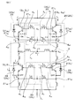
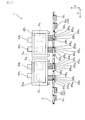
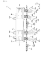
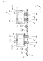
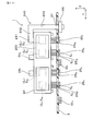
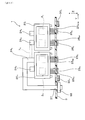
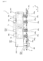
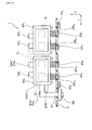
- FIG. 1 is a circuit diagram of a part of the power conversion device when the upper arm semiconductor element is turned on in the first embodiment.
- FIG. 2 is a circuit diagram of a part of the power conversion device when the lower arm semiconductor element is turned on in the first embodiment.
- FIG. 3 is a plan view of a part of the control circuit unit in the first embodiment.
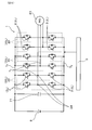
- FIG. 4 is an overall circuit diagram of the power conversion device according to the first embodiment.
- FIG. 5 is a more detailed circuit diagram of the upper arm semiconductor element and the control circuit unit in the first embodiment.
- FIG. 6 is a cross-sectional view of the power conversion device according to the first embodiment, and is a cross-sectional view taken along the line VI-VI in FIG. 7 is a sectional view taken along line VII-VII in FIG.
- FIG. 8 is a plan view of a part of the control circuit unit in the second embodiment.
- FIG. 9 is a plan view of a part of the control circuit unit in the third embodiment.
- FIG. 10 is a plan view of a part of the control circuit unit in the fourth embodiment.
- FIG. 11 is a plan view of a part of the control circuit unit according to the fifth embodiment.
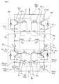
- FIG. 12 is a partial circuit diagram of the power conversion apparatus when the upper arm semiconductor element is turned on in the sixth embodiment.
- FIG. 12 is a partial circuit diagram of the power conversion apparatus when the upper arm semiconductor element is turned on in the sixth embodiment.
- FIG. 13 is a circuit diagram of a part of the power conversion device when the lower arm semiconductor element is turned on in the sixth embodiment.
- FIG. 14 is a schematic cross-sectional view of the power conversion device according to the seventh embodiment.
- FIG. 15 is a plan view of a part of the control circuit unit in the seventh embodiment.
- FIG. 16 is a conceptual diagram of a semiconductor module according to the seventh embodiment.
- FIG. 17 is a schematic cross-sectional view of a power converter according to the eighth embodiment.
- FIG. 18 is a plan view of a part of the control circuit unit in the eighth embodiment.
- FIG. 19 is a schematic cross-sectional view of a power conversion device according to the ninth embodiment.
- FIG. 20 is a plan view of a part of the control circuit unit according to the ninth embodiment.
- FIG. 20 is a plan view of a part of the control circuit unit according to the ninth embodiment.
- FIG. 21 is a conceptual diagram of a semiconductor module in the ninth embodiment.
- FIG. 22 is a plan view of a semiconductor element according to the tenth embodiment.
- FIG. 23 is a cross-sectional view of the upper arm semiconductor module and the control circuit unit in the tenth embodiment.
- FIG. 24 is a cross-sectional view of the lower arm semiconductor module and the control circuit unit in the tenth embodiment.
- FIG. 25 is a schematic cross-sectional view of the power conversion device according to the eleventh embodiment.
- FIG. 26 is a schematic cross-sectional view of the power converter according to the twelfth embodiment.
- FIG. 27 is a conceptual diagram of a semiconductor module in the twelfth embodiment.
- FIG. 28 is a schematic cross-sectional view of a power converter according to the thirteenth embodiment.
- FIG. 29 is a schematic cross-sectional view of a power converter according to the fourteenth embodiment.
- FIG. 30 is a schematic cross-sectional view of the power conversion device according to the fifteenth embodiment.
- FIG. 31 is a schematic cross-sectional view of a power converter according to the sixteenth embodiment.
- FIG. 32 is a schematic cross-sectional view of the power converter according to the seventeenth embodiment.
- FIG. 33 is a schematic cross-sectional view of the power converter according to the eighteenth embodiment.
- FIG. 34 is a schematic cross-sectional view of a power converter according to the nineteenth embodiment.
- FIG. 35 is a schematic cross-sectional view of a power converter according to the twentieth embodiment.
- FIG. 36 is a schematic cross-sectional view of the power converter according to the twenty-first embodiment.
- FIG. 37 is a schematic cross-sectional view of a power converter according to the twenty-second embodiment.
- FIG. 38 is a schematic cross-sectional view of a power converter according to the twenty-third embodiment.
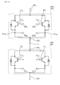
- FIG. 39 is a circuit diagram of a part of the power conversion device when the upper arm semiconductor element is turned on in the comparative example.
- FIG. 40 is a circuit diagram of a part of the power conversion device when the lower arm semiconductor element is turned on in the comparative embodiment.
- the power conversion device can be an on-vehicle power conversion device to be mounted on a vehicle such as an electric vehicle or a hybrid vehicle.
- the power conversion device 1 of this embodiment includes a plurality of semiconductor elements 2 and a control circuit unit 3.
- the semiconductor element 2 includes an upper arm semiconductor element 2 H disposed on the upper arm side and a lower arm semiconductor element 2 L disposed on the lower arm side.
- a plurality of upper arm semiconductor elements 2 H connected in parallel with each other are simultaneously switched by the control circuit unit 3.
- a plurality of lower arm semiconductor elements 2 L connected in parallel with each other are simultaneously switched by the control circuit unit 3.
- the control circuit unit 3 includes a drive circuit 30 connected to a plurality of semiconductor elements 2 that perform switching operations simultaneously, a control wiring 4 G, and a reference wiring 4 KE .
- the control wiring 4 G electrically connects the control electrode 21 G (that is, the gate) of the semiconductor element 2 and the drive circuit 30.
- the reference wiring 4 KE electrically connects the reference electrode 21 KE (that is, the emitter) of the semiconductor element 2 and the drive circuit 30.
- the inductance L KE were parasitic to the reference line 4 KE, are smaller than the inductance L G which is parasitic on the control lines 4 G.
- the power conversion device 1 of this embodiment is a vehicle-mounted power conversion device to be mounted on a vehicle such as an electric vehicle or a hybrid vehicle. As shown in FIG. 4, in this embodiment, two upper arm semiconductor elements 2 H and two lower arm semiconductor elements 2 L are connected in parallel.
- the semiconductor element 2 of this embodiment is an IGBT.
- the semiconductor element 2 is built in the semiconductor module 20 (see FIG. 7).
- One semiconductor module 2 includes an upper arm semiconductor element 2 H and a lower arm semiconductor element 2 L.
- the semiconductor module 20 includes a U-phase semiconductor module 20 u , a V-phase semiconductor module 20 v, and a W-phase semiconductor module 20 w .
- the control circuit unit 3 performs switching operation of the semiconductor element 2 in the semiconductor module 20 to convert the DC power supplied from the DC power supply 8 into AC power. And the three-phase alternating current motor 81 is driven using this alternating current power, and the said vehicle is drive
- the semiconductor module 20 includes a main body portion 200 containing the semiconductor element 2, a power terminal 24 protruding from the main body portion 200, and a control terminal 25.
- the power terminal 24 includes a positive terminal 24 P and a negative terminal 24 N to which a DC voltage is applied, and an output terminal 24 O that outputs AC power.
- the control terminal 25 is connected to the control circuit unit 3.
- the semiconductor element 2 has a sense electrode 21 SE in addition to the control electrode 21 G and the reference electrode 21 KE .
- the semiconductor module 20 has a built-in temperature sensitive diode 29.
- the cathode electrode 21 K of the temperature sensitive diode 29 is connected to the reference electrode 21 KE .
- the anode electrode 21 A and the cathode electrode 21 K of the temperature sensitive diode 29 and the electrodes 21 G , 21 KE , and 21 SE of the semiconductor element 2 are electrically connected to the control circuit unit 3 via the control terminal 25. .
- the anode electrode 21 A and the cathode electrode 21 K are connected to the temperature detection circuit 38, and the sense electrode 21 SE is connected to the current detection circuit 39.
- the temperature detection circuit 38 measures the temperature of the semiconductor element 2 by measuring the forward voltage of the temperature sensitive diode 29.
- the current detection circuit 39 measures the current flowing through the entire semiconductor element 2 by measuring the current flowing through the sense electrode 21 SE .
- the control circuit portion 3 is formed with a plurality of connection portions 5 (through holes in this embodiment) for electrically connecting the control circuit portion 3 to the semiconductor element 2.
- a control terminal 25 is inserted into this connecting portion 5 and soldered.
- the control circuit unit 3 a connecting portion 5, and the reference connection portion 5 KE for connection to the reference electrode 21 KE, and a control connection section 5 G for connection to the control electrode 21 G, the sense electrodes 21 SE And a sense connection section 5 SE for connection.
- the control circuit unit 3 includes an anode connecting portion 5 A for connection to the anode electrode 21 A, and a cathode connecting portion 5 K for connection to the cathode electrode 21 K.
- the driving circuit 30 and the reference connection portion 5 KE they are connected by standard wiring 4 KE.
- a drive circuit 30 and the control connection unit 5 G are connected by control lines 4 G.
- the wiring length of the reference wiring 4KE is shorter than the wiring length of the control wiring 4G . Accordingly, the inductance L KE were parasitic to the reference line 4 KE, it is smaller than the inductance L G which is parasitic on the control lines 4 G.
- the reference electrode 21 KE two upper arms semiconductor element 2 H are electrically connected by the AC busbars 7 A. Inductance is parasitic in the AC bus bar 7 A.
- a free wheel diode 28 is connected in reverse parallel to each semiconductor element 2.
- the upper arm semiconductor element 2 H and the lower arm semiconductor element 2 L both from the off state, consider the case where switching to the state of turning on the upper arm semiconductor element 2 H.
- a freewheeling current (not shown) is sequentially applied to the free wheel diode 28 of the lower arm semiconductor element 2 L due to the influence of the inductance of the three-phase AC motor 81 (see FIG. 4). Flowing in the direction.
- the current I flows, and the reflux current gradually decreases. Then, to recover free-wheel diodes 28, flows recovery current I r is.
- one free wheel diode 28 a may recover quickly and the other free wheel diode 28 b may not recover.
- the currents I of the two upper arm semiconductor elements 2 H both flow through one free wheel diode 28 a . Therefore, the current I flowing through the other upper arm semiconductor element 2 Hb passes through the AC bus bar 7 A and flows through the one free wheel diode 28 a .
- the inductance is parasitic in the AC bus bar 7 A , an induced electromotive force V KE is generated by this inductance. Therefore, the reference electrode 21 KEb of the other upper arm semiconductor element 2 Hb is higher in potential by V KE than the reference electrode 21 KEa of one upper arm semiconductor element 2 Ha .
- the drive circuit 30 applies a control voltage V G to the control electrode 21 G with reference to the potential E H. Therefore, the sum V G + ⁇ V of the control voltages V G and ⁇ V is applied to the control electrode 21 G of the semiconductor element 2 Ha having a low reference potential.
- the negative arm terminal 24 N of the semiconductor module 20 is connected to the lower arm semiconductor element 2 L.
- An inductance L N is parasitic on the negative terminal 24 N.
- the inductances L N of the two negative terminals 24 N may be different from each other.
- the inductance L Nb parasitic on the other negative electrode terminal 24 Nb may be higher than the inductance L Na parasitic on one negative electrode terminal 24 Na .
- the reference electrode 21 KEb of the other lower arm semiconductor element 2 Lb has a higher potential than the reference electrode 21 KEa of one lower arm semiconductor element 2 La .
- the stacked body 10 is configured by alternately stacking the semiconductor modules 20 and the cooling pipes 11.
- a pressure member 17 (for example, a leaf spring) is disposed at a position adjacent to the stacked body 10 in the stacking direction of the stacked body 10 (hereinafter also referred to as the X direction).
- the pressurizing member 17 presses the laminated body 10 toward the wall portion 161 of the case 16. Thereby, the laminated body 10 is fixed in the case 16 while ensuring a contact pressure between the semiconductor module 20 and the cooling pipe 11.
- an end cooling pipe 11 a located at one end in the X direction includes an introduction pipe 13 for introducing the refrigerant 12 and a lead-out pipe 14 for leading out the refrigerant 12. Connected. When the refrigerant 12 is introduced from the introduction pipe 13, the refrigerant 12 flows through all the cooling pipes 11 through the connection pipe 15. Thereby, the semiconductor module 20 is cooled.
- the semiconductor module 20 includes the positive terminal 24 P , the negative terminal 24 N , the output terminal 24 O, and the control terminal 25.
- the positive terminal 24 P and the capacitor 72 are connected by a positive bus bar 7 P.
- the negative electrode terminal 24 N and the capacitor 72 are connected by a negative electrode bus bar 7 N.
- the control terminal 25 is connected to the connection portion 5 of the control circuit portion 3.
- a plurality of connection portions 5 constitute a connection portion group 50.
- the drive circuit 30 is formed at a position adjacent to the connection portion group 50 in the arrangement direction of the plurality of connection portions 5 (hereinafter also referred to as Y direction).
- the control circuit section 3, as the connection unit 5 includes a reference connection portion 5 KE and the control connection 5 G.
- the driving circuit 30 and the reference connection portion 5 KE they are connected by standard wiring 4 KE.
- a drive circuit 30 and the control connection unit 5 G are connected by control lines 4 G.
- the reference connection portion 5 KE rather than control connection unit 5 G, is formed at a position closer to the drive circuit 30 to which they are connected. More specifically, the connection portion 5 formed at a position closest to the drive circuit 30 in the Y direction among the plurality of connection portions 5 is referred to as a reference connection portion 5KE .
- connection portion group 50 includes an upper arm connection portion group 50 H for connection to the upper arm semiconductor element 2 H and a lower arm connection portion group 50 for connection to the lower arm semiconductor element 2 L. There is L.
- the upper arm connection portion group 50 H and the lower arm connection portion group 50 L are adjacent to each other in the Y direction.
- the drive circuit 30 includes an upper arm drive circuit 30 H connected to the upper arm semiconductor element 2 H and a lower arm drive circuit 30 L connected to the lower arm semiconductor element 2 L.
- the upper arm drive circuit 30 H and the lower arm drive circuit 30 L are formed at positions sandwiching the upper arm connection portion group 50 H and the lower arm connection portion group 50 L from the Y direction.
- the inductance L KE were parasitic to the reference line 4 KE, it is smaller than the inductance L KE were parasitic on the control lines 4 G. Therefore, it is possible to reduce variations in voltage applied to the control electrode 21 G of each semiconductor element 2. That is, as described above, when a plurality of semiconductor elements 2 connected in parallel are simultaneously switched, the reference potentials of the individual semiconductor elements 2 are likely to vary. As a result, the current i may flow from the semiconductor element 2 having a high reference potential to the semiconductor element 2 having a low reference potential through the reference wiring 4KE .
- the inductance L KE parasitic to the reference line 4 KE is larger than the inductance L G parasitic on control lines 4 G. Therefore, a high induced electromotive force ⁇ V is generated when the current i flows through the reference wiring 4KE . Therefore, when a plurality of upper arm semiconductor elements 2 H are simultaneously turned on, a high voltage V G + ⁇ V is applied to some upper arm semiconductor elements 2 Ha , and this semiconductor element 2 Ha is likely to deteriorate, Only a low voltage V G ⁇ V is applied to the arm semiconductor element 2 Hb , which causes a problem that the arm semiconductor element 2 Hb does not turn on sufficiently. As shown in FIG.
- the wiring length of the reference wiring 4KE is made shorter than the wiring length of the control wiring 4G . Therefore, the inductance L KE parasitic to the reference line 4 KE, certainly, can be smaller than the inductance L G parasitic on control lines 4 G.
- connection portions 5 are formed in the control circuit portion 3.
- the drive circuit 30 is formed at a position adjacent to the connection unit group 50 in the Y direction.
- Reference connection portion 5 KE, in the Y direction, than the control connection section 5 G, is formed at a position closer to the drive circuit 30. Therefore, it is possible to shorten the reference length of the wiring 4 KE connecting the driving circuit 30 and the reference connection portion 5 KE, it is possible to reduce the inductance L KE parasitic to the reference line 4 KE.
- connection portion 5 formed at a position closest to the drive circuit 30 in the Y direction among the plurality of connection portions 5 is defined as a reference connection portion group 5KE . Therefore, it is possible to shorten the length of the reference line 4 KE, the inductance of the reference line 4 KE can be effectively reduced.
- the upper arm semiconductor element 2 H and the lower arm semiconductor element 2 L are built in the same semiconductor module 20. Therefore, the effect of the present invention can be exhibited particularly remarkably. That is, as shown in FIG. 12, the upper arm semiconductor element 2 H and the lower arm semiconductor element 2 L, although it is also possible to incorporate into separate semiconductor module 20, in this case, the upper arm semiconductor element 2 H
- the voltage applied to the control electrode 21 G is not likely to vary greatly. That is, in this case, the two upper arm semiconductor elements 2 H are not individually connected to the lower arm semiconductor element 2 L, but are connected to the lower arm semiconductor element 2 L only through the common AC bus bar 7 A. Electrically connected.
- a power conversion device capable of simultaneously switching a plurality of semiconductor elements and reducing variations in voltage applied to the control electrodes of the individual semiconductor elements.
- the present invention is not limited thereto . That is, only one of the upper arm and the lower arm may be an inductance L KE reference wiring 4 KE smaller than the inductance L G of the control wire 4 G.
- Embodiment 2 This embodiment is an example in which the configuration of the control circuit unit 5 is changed. As shown in FIG. 8, in this embodiment, the width of the reference wiring 4KE is made larger than the width of the control wiring 4G . Accordingly, the inductance L KE parasitic to the reference line 4 KE, is smaller than the inductance L G parasitic on control lines 4 G.
- the reference wiring 4 KE of Indakuntasu L KE control wire 4 G it can be smaller than the inductance L G.
- the same configuration and operational effects as those of the first embodiment are provided.
- control wiring 4G is shorter than the reference wiring 4KE , but the present invention is not limited to this. That is, as in the first embodiment (see FIG. 3), the reference wiring 4KE may be shorter than the control wiring 4G , and the reference wiring 4KE may be wider than the control wiring 4G. . In this way, it can reduce the wiring length of the reference line 4 KE, and since the width can thick, it is possible to effectively reduce the inductance L KE reference wiring 4 KE.
- This embodiment is an example in which the configuration of the control circuit unit 3 is changed. As shown in FIG. 9, in this embodiment, two drive circuits 30 H and 30 L are formed between the upper arm connection portion group 50 H and the lower arm connection portion group 50 L. The individual drive circuits 30 H and 30 L are formed at positions adjacent to the connection portion group 50 in the Y direction. In addition, the same configuration and operational effects as those of the first embodiment are provided.
- This embodiment is an example in which the configuration of the control circuit unit 3 is changed.
- the individual drive circuits 30 H and 30 L are arranged on one side of the connection group 50 in the Y direction. That is, the upper arm drive circuit 30 H is disposed on one side of the upper arm connection portion group 50 H in the Y direction, and the lower arm drive circuit 30 L is disposed on one side of the lower arm connection portion group 50 L in the Y direction. It is arranged on the side.
- the same configuration and operational effects as those of the first embodiment are provided.
- This embodiment is an example in which the configuration of the control circuit unit 3 is changed.
- the upper arm connection portion group 50 H and the lower arm connection portion group 50 L are alternately arranged in the X direction.
- the drive circuits 30 H and 30 L are arranged on one side of the connection group 50 H and 50 L in the Y direction.
- the reference wiring 4KE is shorter than the control wiring 4G as in the first embodiment. Accordingly, the inductance L KE parasitic to the reference line 4 KE, is smaller than the inductance L G parasitic on control lines 4 G.
- the same configuration and operational effects as those of the first embodiment are provided.
- This embodiment is an example in which the configuration of the semiconductor module 20 is changed.
- the upper arm semiconductor element 2 H and the lower arm semiconductor element 2 L are built in different semiconductor modules 20.
- the difference is less likely to occur to the potential of the reference electrode 21 KE plurality of upper arm semiconductor element 2 H (see FIG. 12)
- the potential of the reference electrode 21 KE of the lower arm semiconductor element 2 L May make a difference. That is, the reference electrode 21 KE of the lower arm semiconductor element 2 L connects the negative terminal 24 N, there is the inductance L N of the negative terminal 24 N varies.
- the inductance L Nb of the other lower arm semiconductor element 2 Lb may be larger than the inductance L Na of one lower arm semiconductor element 2 La .
- the lower arm semiconductor element 2 Lb of the other lower arm semiconductor element 2 La than the lower arm semiconductor element 2 La of one is caused by the difference between the inductances L Na and L Nb.
- the potential of the reference electrode 21KE increases. Therefore, to the other one of the lower arm semiconductor element 2 La from the lower arm semiconductor element 2 Lb, the current i flows through the reference wire 4 KE, induced electromotive force ⁇ V is generated in the reference wiring 4 KE.
- the arrangement position of the control circuit unit 30 is changed.
- the upper arm semiconductor element 2 H and the lower arm semiconductor element 2 L are provided in different semiconductor modules 20 (20 H , 20 L ).
- the upper arm semiconductor module 20 H of this embodiment incorporates a plurality of upper arm semiconductor elements 2 H (2 Ha , 2 Hb ) connected in parallel to each other and simultaneously performing switching operation.
- the lower arm semiconductor module 20 L includes a plurality of lower arm semiconductor elements 2 L (2 La , 2 Lb ) that are connected in parallel to each other and simultaneously perform switching operations.
- the upper arm drive circuit 30 H and the lower arm drive circuit 30 L are arranged between the upper arm connection unit group 50 H and the lower arm connection unit group 50 L in the Y direction. Yes.
- the reference connecting portion 5KE and the drive circuit 30 are connected by the reference wiring 4KE .
- the control connecting portion 5G and the drive circuit 30 are connected by the control wiring 4G .
- the reference connection portion 5 KE is formed at a position close to the driving circuit 30 connected thereto. More specifically, the connection portion 5 formed at a position closest to the drive circuit 30 in the Y direction among the plurality of connection portions 5 is referred to as a reference connection portion 5KE .
- the upper arm drive circuit 30 H and the lower arm drive circuit 30 L are arranged between the upper arm connection portion group 50 H and the lower arm connection portion group 50 L in the Y direction.
- a power supply circuit 31 connected to these is provided between the upper arm drive circuit 30 H and the lower arm drive circuit 30 L.
- the power supply circuit 31 is used in common for the two drive circuits 30 H and 30 L.
- the drive circuit 30 of this embodiment is configured by a dedicated IC.
- an insulating space S I to ensure these insulating is formed.
- a low voltage wiring 89 is provided at the edge 35 of the control circuit unit 3. Also between the low-pressure line 89 and the connection portion group 50, an insulating space S I is formed.
- the reference connection portion 5 KE than the control connection section 5 G, is formed at a position closer to the drive circuit 30. Therefore, the reference wiring 4KE can be made shorter than the control wiring 4G, and the inductance LKE parasitic on the reference wiring 4KE can be reduced.
- the two drive circuits 30 H and 30 L are arranged between the upper arm connection portion group 50 H and the lower arm connection portion group 50 L in the Y direction. Therefore, the upper arm drive circuit 30 H and the lower arm drive circuit 30 L can be brought close to each other, and the power supply circuit 31 can be used in common for the two drive circuits 30 H and 30 L. Therefore, the number of power supply circuits 31 can be reduced, and the manufacturing cost of the control circuit unit 3 can be reduced. In addition, the area of the control circuit unit 3 can be reduced.
- each connection portion 5 is connected to different electrodes 21 (21 KE , 21 SE , 21 G , 21 A , 21 K : see FIG. 5) of the semiconductor element 2.
- the individual connection portions 5 constituting the upper arm connection portion group 50 H as viewed from the one side in the Y direction (for example, the left side in the drawing) toward the other side (for example, the right side in the drawing)
- the upper arm connection portion group 50 H and the lower arm connection portion group 50 L can be made symmetrical while the reference connection portion 5KE is brought close to the control circuit 30. Therefore, the configuration of the control circuit board 3 can be simplified and the design can be facilitated. In addition, the same configuration and operational effects as those of the first embodiment are provided.
- the arrangement position of the drive circuit 30 is changed.
- the reference connection portion 5KE is formed at a position closer to the drive circuit 30 connected thereto than the control connection portion 5G. It is. Thereby, the reference wiring 4KE is made shorter than the control wiring 4G , and the inductance LKE of the reference wiring 4KE is made small.
- the upper arm drive circuit 30 H , the upper arm connection unit group 50 H , the lower arm connection unit group 50 L, and the lower arm drive circuit 30 L are arranged in the Y direction. Are arranged in this order.
- the insulating region S I to isolate these are formed. Further, the low voltage wiring 89 is provided on the edge 35 of the control circuit unit 3 as in the seventh embodiment. An insulating region S I is also formed between the low-voltage wiring 89 and the drive circuit 30 H.
- the control circuit unit 3 can be symmetric between the upper arm side and the lower arm side, and the circuit configuration of the control circuit unit 3 can be simplified. Therefore, the control circuit unit 3 can be easily designed. Further, with the above configuration, the control circuit unit 3 can be further downsized. That is, as shown in FIG. 15, the drive circuits 30 H and 30 L can be provided between the two connection portion groups 50 H and 50 L. In this case, the connection portion group 50 and the low-voltage wiring 89 are connected to each other.
- the drive circuit 30 is arranged outside the connection portion group 50 in the Y direction as in the present embodiment, the drive circuit 30 is interposed between the connection portion group 50 and the low-voltage wiring 89.
- the wiring 89 can be moved away from the connection unit group 50. Therefore, unlike the seventh embodiment (see FIG. 15), there is no need to form a dedicated insulating region S I ′ for insulating between the connecting portion group 50 and the low-voltage wiring 89, and the area of the control circuit portion 3 can be reduced. Can be made smaller.
- the same configuration and operational effects as those of the first embodiment are provided.
- the upper arm drive circuit 30 H , the upper arm connection unit group 50 H , the lower arm drive circuit 30 L, and the lower arm connection unit group 50 are arranged in the Y direction.
- L is arranged in this order.
- the reference connection portion 5 KE, than the control connection section 5 G, is arranged at a position close to the control circuit 30. Thereby, the reference wiring 4KE is made shorter than the control wiring 4G , and the inductance LKE of the reference wiring 4KE is made small.
- a plurality of upper arm semiconductor elements 2 H (2 Ha , 2 Hb ) and a plurality of lower arm semiconductor elements 2 L (2 La , 2 Lb ) connected in parallel to each other. are provided in the same semiconductor module 20, but the present invention is not limited to this. That is, the individual semiconductor elements 2 (2 H , 2 L ) may be incorporated in separate semiconductor modules 20, and these semiconductor modules 20 may be connected to the control circuit unit 3 shown in FIG. Alternatively, one semiconductor module 20 may include one upper arm semiconductor element 2 H and one lower arm semiconductor element 2 L, and the semiconductor module 20 may be connected to the control circuit unit 3 shown in FIG.
- the semiconductor element 2 of this embodiment includes a plurality of pads 26 for electrical connection to the control circuit unit 3.
- the plurality of pads 26 are arranged in the Y direction.
- two pads 26 are reference pads 26 KE (26 KEa , 26 KEb ) for electrically connecting the reference electrode 21 KE of the semiconductor element 2 to the control circuit unit 3.
- the reference pad 26 KE arranged at a position close to the drive circuit 30 in the Y direction is used as the control circuit unit 3. Is electrically connected.
- the semiconductor module 20 includes a main body 200 that contains the semiconductor element 2.
- a plurality of control terminals 25 protrude from the main body 200.
- the semiconductor element 2 the first reference pad 26 KEA and second reference pads 26 Keb, 2 pieces of reference pads 26 KE is formed.
- the upper arm semiconductor module 20 H, toward the second reference pads 26 Keb is than the first reference pad 26 KEA, it is arranged at a position closer to the upper arm drive circuit 30 H in the Y direction ing.
- the second reference pad 26 KEb is connected to the reference control terminal 25 KE using a wire 201.
- the second reference pad 26 KEb is electrically connected to the control circuit unit 3.
- the lower arm semiconductor element 2 L, toward the first reference pad 26 KEA is than the second reference pads 26 Keb, disposed at a position closer to the lower arm drive circuit 30 L Yes.
- the first reference pad 26 KEa is connected to the reference control terminal 25 KE using a wire 201.
- the first reference pad 26 KEa is electrically connected to the control circuit unit 3.
- the upper arm semiconductor element 2 H and the lower arm semiconductor element 2 L can have the same structure, and the reference control terminal is located at a position close to the drive circuit 30 on each of the upper arm side and the lower arm side. 25 KE can be provided. Therefore, while using the same type of semiconductor element 2 H, 2 L, it is possible to shorten the upper arm and the lower arm, the reference wiring 4 KE length, respectively. Therefore, the types of semiconductor elements 2 to be used can be reduced, the manufacturing cost of the power converter 1 can be reduced, and the inductance L KE of the reference wiring 4 KE can be reduced. In addition, the same configuration and operational effects as those of the first embodiment are provided.
- Embodiment 11 This embodiment is an example in which the configuration of the semiconductor module 20 is changed. As shown in FIG. 25, as in Embodiment 1 in the present embodiment, arranged in the Y direction, the reference connection portion 5 KE, in than the control connection section 5 G, located close to the driving circuit 30 to which they are connected It is. Thereby, the length of the reference wiring 4KE is shortened, and the inductance LKE of the reference wiring 4KE is reduced.
- the upper arm semiconductor module 20 H and the lower arm semiconductor module 20 L are arranged in the Y direction. Then, the upper arm semiconductor module 20 H is positioned 180 ° around the rotation axis A that exists between the two semiconductor modules 20 H and 20 L and is parallel to the protruding direction of the control terminal 25 (hereinafter also referred to as Z direction).
- the lower arm semiconductor module 20 L is connected to the control circuit unit 3 in an inverted posture. In this way, the same type of semiconductor module 20 can be used as the upper arm semiconductor module 20 H and the lower arm semiconductor module 20 L. Therefore, the types of semiconductor modules 20 to be used can be reduced, and the manufacturing cost of the power conversion device 1 can be reduced.
- the reference control terminal 25KE can be brought close to the drive circuit 30 for each of the upper arm side and the lower arm side while using the same type of semiconductor module 20. Therefore, it is possible to shorten the reference line 4 KE, can reduce the inductance L KE reference wiring 4 KE.
- the same configuration and operational effects as those of the first embodiment are provided.
- Embodiment 12 This embodiment is an example in which the type of the semiconductor module 2 is changed.
- two upper arm semiconductor elements 2 H connected in parallel to each other are provided in one upper arm semiconductor module 20 H.
- two lower arm semiconductor elements 2 L connected in parallel to each other are provided in one lower arm semiconductor module 20 L.
- These semiconductor modules 20 H and 20 L include two collector terminals 24 C (24 Ca and 24 Cb ) and one emitter terminal 24 E.
- the emitter terminal 24 E is disposed between the two collector terminals 24 C.
- the upper arm semiconductor module 20 H and the lower arm semiconductor module 20 L are arranged in the Y direction as in the eleventh embodiment. Then, the lower arm semiconductor module 20 L is arranged in a posture in which the upper arm semiconductor module 20 H is rotated by 180 ° around the rotation axis A that exists between the two semiconductor modules 20 H and 20 L and is parallel to the Z direction. Is connected to the control circuit section 3. In addition, the same configuration and operational effects as those of the first embodiment are provided.
- This embodiment is an example in which the configuration of the semiconductor module 20 is changed.
- two upper arm semiconductor elements 2 H (2 Ha , 2 Hb ) connected in parallel to each other and two lower arm semiconductor elements 2 L ( 2 La and 2 Lb ) are provided in one semiconductor module 20.
- the output terminal 24 O of the semiconductor module 20 includes a first portion 241 that protrudes from the main body portion 200 to the side opposite to the control circuit portion 3, a second portion 242 that extends from the first portion 241 in the Y direction, A third portion 243 projecting from the second portion 242 to the control circuit portion 3 side in the Z direction.
- a through hole 37 is formed in the control circuit unit 3.
- a third portion 243 is inserted into the through hole 37.
- a current sensor 88 for measuring the output current is attached to the third portion 243.
- the same configuration and operational effects as those of the first embodiment are provided.
- FIG. 15 This embodiment is an example in which the structure of the semiconductor module 20 is changed.
- two upper arm semiconductor elements 2 H connected in parallel to each other, and two lower arm semiconductor elements 2 L connected in parallel to each other, Are provided in one semiconductor module 20.
- the output terminal 24 O protrudes from the main body 200 to the control circuit unit 3 side in the Z direction.
- a through hole 37 is formed in the control circuit unit 3, and an output terminal 24 O is inserted into the through hole 37.
- a current sensor 88 for measuring an output current is attached to the output terminal 24 O.
- the same configuration and operational effects as those of the first embodiment are provided.
- This embodiment is an example in which the configuration of the semiconductor module 20 is changed. As shown in FIG. 31, the output terminal 24 O of this embodiment protrudes from the side surface 209 of the main body 200 and is bent. The tip of the output terminal 24 O is inserted into the through hole 37 of the control circuit unit 3. A current sensor 88 is attached to the output terminal 24 O. In addition, the same configuration and operational effects as those of the first embodiment are provided.
- This embodiment is an example in which the configuration of the semiconductor module 20 is changed.
- the upper arm semiconductor element 2 H and the lower arm semiconductor element 2 L are provided in separate semiconductor modules 20.
- the emitter terminal 24 E of the upper arm semiconductor module 20 H and the collector terminal 24 C of the lower arm semiconductor module 20 L are connected to each other by an AC bus bar 7 A.
- the emitter terminal 24 E of the upper arm semiconductor module is bent and inserted into the through hole 37 of the control circuit unit 3.
- This emitter terminal 24 E is mounted a current sensor 88 for measuring the output current.
- the same configuration and operational effects as those of the first embodiment are provided.
- the upper arm semiconductor element 2 H and the lower arm semiconductor element 2 L are provided in different semiconductor modules 20, respectively.
- the upper arm semiconductor module 20 H includes two emitter terminals 24 E , a first emitter terminal 24 Ea and a second mitter terminal 24 Eb .
- the first emitter terminal 24 Ea and the collector terminal 24 C of the lower arm semiconductor module 20 L are connected by an AC bus bar 7 A.
- the second emitter terminal 24 Eb protrudes from the main body portion 200 of the upper arm semiconductor module 20 H to the control circuit portion 3 side in the Z direction.
- the second emitter terminal 24 Eb is inserted into the through hole 37 of the control circuit unit 3.
- a current sensor 88 is attached to the second emitter terminal 24 Eb .
- the same configuration and operational effects as those of the first embodiment are provided.
- This embodiment is an example in which the configuration of the semiconductor module 20 is changed.
- the upper arm semiconductor element 2 H and the lower arm semiconductor element 2 L are provided in separate semiconductor modules 20.
- the first emitter terminal 24 Ea of the upper arm semiconductor module 20 H and the collector terminal 24 C of the lower arm semiconductor module 20 L are connected by an AC bus bar 7 A.
- a second emitter terminal 24 Eb protrudes from the side surface 209 of the main body 200 of the upper arm semiconductor module 20 H.
- the second emitter terminal 24 Eb is bent and inserted into the through hole 37 of the control circuit unit 3.
- a current sensor 88 is attached to the second emitter terminal 24 Eb .
- the same configuration and operational effects as those of the first embodiment are provided.
- FIG. 35 which is an example in which the configuration of the semiconductor module 20 is changed
- the upper arm semiconductor element 2 H and the lower arm semiconductor element 2 L are provided in different semiconductor modules 20. is there.
- the collector terminal 24 C of the lower arm semiconductor element 2 L protrudes from the main body 200 and is bent.
- the collector terminal 24 C is inserted into the through hole 37 of the control circuit unit 3.
- a current sensor 88 is attached to the collector terminal 24.
- the same configuration and operational effects as those of the first embodiment are provided.
- FIG. 21 This embodiment is an example in which the configuration of the semiconductor module 20 is changed.
- the upper arm semiconductor element 2 H and the lower arm semiconductor element 2 L are provided in separate semiconductor modules 20.
- the lower arm semiconductor module 2 L includes two collector terminals 24 C including a first collector terminal 24 Ca and a second collector terminal 24 Cb .
- the emitter terminal 24 E of the upper arm semiconductor module 20 H and the first collector terminal 24 Ca of the lower arm semiconductor module 20 L are connected by an AC bus bar 7 A.
- the second collector terminal 24 Cb of the lower arm semiconductor module 20 L protrudes from the main body portion 200 toward the control circuit portion 3 and is inserted into the through hole 37.
- a current sensor 88 is attached to the second collector terminal 24 Cb .
- the same configuration and operational effects as those of the first embodiment are provided.
- the lower arm semiconductor module 20 L of the present embodiment includes two collector terminals 24 C , a first collector terminal 24 Ca and a second collector terminal 24 Cb .
- the first collector terminal 24 Ca is connected to the emitter terminal 24 E of the upper arm semiconductor module 20 H.
- the second collector terminal 24 Cb protrudes from the side surface 209 of the main body 200 and is bent.
- the second collector terminal 24 Cb is inserted into the through hole 37 of the control circuit unit 3.
- a current sensor 88 is attached to the second collector terminal 24 Cb .
- the same configuration and operational effects as those of the first embodiment are provided.
- This embodiment is an example of changing the configuration of the AC bus bar 7 A.
- the AC bus bar 7 A of this embodiment connects the emitter terminal 24 E of the upper arm semiconductor module 20 H and the collector terminal 24 C of the lower arm semiconductor module 20 L.
- the AC bus bar 7 A is bent and inserted into the through hole 37 of the control circuit unit 3.
- a current sensor 88 is attached to the AC bus bar 7A.
- the same configuration and operational effects as those of the first embodiment are provided.
Landscapes
- Engineering & Computer Science (AREA)
- Power Engineering (AREA)
- Inverter Devices (AREA)
Abstract
複数の半導体素子(2)と、制御回路部(3)とを備える。並列接続された複数の半導体素子(2)を、同時にスイッチング動作するよう構成されている。制御回路部(3)は、同時に動作する複数の半導体素子(2)に接続した駆動回路(30)と、制御配線(4G)と、基準配線(4KE)とを備える。制御配線(4G)は、半導体素子(2)の制御電極(21G)と駆動回路(30)とを接続している。基準配線(4KE)は、半導体素子(2)の基準電極(21KE)と駆動回路(30)とを接続している。基準配線(4KE)に寄生したインダクタンス(LKE)を、制御配線(4G)に寄生したインダクタンス(LG)よりも小さくしてある。
Description
本出願は、2016年3月28日に出願された日本出願番号2016-63541号と、2017年2月28日に出願された日本出願番号2017-36745号に基づくもので、ここにその記載内容を援用する。
本開示は、複数の半導体素子と、該半導体素子のスイッチング動作を制御する制御回路部とを備える電力変換装置に関する。
直流電力と交流電力との間で電力変換を行う電力変換装置として、IGBT等の半導体素子と、該半導体素子に電気接続した制御回路部とを備えるものが知られている(下記特許文献1参照)。この電力変換装置は、上記制御回路部によって半導体素子をスイッチング動作させることにより、直流電力を交流電力に変換するよう構成されている。
制御回路部には、半導体素子を駆動する駆動回路が形成されている。また、制御回路部は、半導体素子の基準電極(すなわち、エミッタ)と上記駆動回路とを繋ぐ基準配線と、半導体素子の制御電極(すなわち、ゲート)と駆動回路とを繋ぐ制御配線とを備える。駆動回路は、上記基準電極の電位を基準として、制御電極に、予め定められた制御電圧を加えるよう構成されている。これにより、半導体素子をオンしている。
近年、より高い出力電流を得ることが可能な電力変換装置が望まれている。そのため、複数の半導体素子を並列接続し、これら複数の半導体素子を同時にスイッチング動作させることが検討されている。これにより、個々の半導体素子に流せる電流は少なくても、電力変換装置全体として、多くの電流を流せるようにすることが検討されている。
しかしながら、複数の半導体素子を同時にスイッチング動作させると、半導体素子の制御電極に加わる電圧がばらつきやすくなる。すなわち、上記構成にした場合、1個の駆動回路が複数の半導体素子に電気接続することになる。また、複数の半導体素子を同時にスイッチング動作させると、後述するように、半導体素子に逆並列接続したフリーホイールダイオードのリカバリー特性のばらつき等が原因となって、半導体素子の上記基準電極の電位(以下、基準電位とも記す)がばらつく可能性がある。そのため、基準電位が高い半導体素子から基準電位が低い半導体素子へ、上記基準配線を介して電流iが流れる可能性がある。この場合、基準配線に寄生するインダクタンスLKEが原因となって、誘導起電力ΔV(=LKEdi/dt)が発生する。
そのため、基準電位が低い半導体素子の基準電極から見ると、駆動回路の基準となる電位が、ΔVだけ高くなってしまう(図39参照)。したがって、基準電位が低い半導体素子の制御電極には、駆動回路から発生する制御電圧VGとΔVとの和(VG+ΔV)が加わってしまう。そのため、通常の制御電圧VGよりも高い電圧が制御電極に加わり、この半導体素子が劣化する可能性が考えられる。
また、基準配線に誘導起電力ΔVが発生すると、基準電位が高い半導体素子の基準電極から見ると、駆動回路の基準となる電位が、ΔVだけ低下してしまう(図39参照)。したがって、基準電位が高い半導体素子の制御電極には、VG-ΔVしか電圧が加わらない。そのため、この半導体素子が十分にオンせず、電流量が低下しやすい。
本開示は、複数の半導体素子を同時にスイッチング動作でき、かつ個々の半導体素子の制御電極に加わる電圧のばらつきを低減できる電力変換装置を提供することを目的とする。
本開示の第1の態様は、複数の半導体素子と、
該半導体素子のスイッチング動作を制御する制御回路部とを備え、
上記半導体素子には、上アーム側に配された上アーム半導体素子と、下アーム側に配された下アーム半導体素子とがあり、上記制御回路部によって、互いに並列に接続された複数の上記上アーム半導体素子を同時にスイッチング動作すると共に、互いに並列に接続された複数の上記下アーム半導体素子を同時にスイッチング動作するよう構成され、
上記制御回路部は、同時にスイッチング動作する複数の上記半導体素子にそれぞれ電気接続した駆動回路と、上記半導体素子の制御電極と上記駆動回路とを繋ぐ制御配線と、上記半導体素子の基準電極と上記駆動回路とを繋ぐ基準配線とを備え、
該基準配線に寄生したインダクタンスを、上記制御配線に寄生したインダクタンスよりも小さくしてある、電力変換装置にある。
該半導体素子のスイッチング動作を制御する制御回路部とを備え、
上記半導体素子には、上アーム側に配された上アーム半導体素子と、下アーム側に配された下アーム半導体素子とがあり、上記制御回路部によって、互いに並列に接続された複数の上記上アーム半導体素子を同時にスイッチング動作すると共に、互いに並列に接続された複数の上記下アーム半導体素子を同時にスイッチング動作するよう構成され、
上記制御回路部は、同時にスイッチング動作する複数の上記半導体素子にそれぞれ電気接続した駆動回路と、上記半導体素子の制御電極と上記駆動回路とを繋ぐ制御配線と、上記半導体素子の基準電極と上記駆動回路とを繋ぐ基準配線とを備え、
該基準配線に寄生したインダクタンスを、上記制御配線に寄生したインダクタンスよりも小さくしてある、電力変換装置にある。
上記電力変換装置では、基準配線に寄生したインダクタンスを、制御配線に寄生したインダクタンスよりも小さくしてある。
そのため、個々の半導体素子の制御電極に加わる電圧のばらつきを低減することができる。すなわち、上述したように、互いに並列に接続された複数の半導体素子を同時にスイッチング動作させると、個々の半導体素子の基準電位がばらつきやすくなる。その結果、基準電位が高い半導体素子から基準電位が低い半導体素子へ、基準配線を介して電流が流れることがある。しかしながら、本形態では、基準配線に寄生したインダクタンスを小さくしてあるため、電流が流れたときに基準配線に発生する誘導起電力ΔVを小さくすることができる。上述したように、基準電位が低い半導体素子は、制御電極にVG+ΔVが加わり、基準電位が高い半導体素子にはVG-ΔVが加わるが、本形態ではΔVを小さくすることができるため、各半導体素子の制御電極に加わる電圧のばらつきを抑制できる。そのため、基準電位が低い半導体素子の制御電極に高い電圧が加わりすぎて、この半導体素子が劣化したり、基準電位が高い半導体素子の制御電極に低い電圧しか加わらず、充分にオンしなかったりする不具合を抑制できる。
そのため、個々の半導体素子の制御電極に加わる電圧のばらつきを低減することができる。すなわち、上述したように、互いに並列に接続された複数の半導体素子を同時にスイッチング動作させると、個々の半導体素子の基準電位がばらつきやすくなる。その結果、基準電位が高い半導体素子から基準電位が低い半導体素子へ、基準配線を介して電流が流れることがある。しかしながら、本形態では、基準配線に寄生したインダクタンスを小さくしてあるため、電流が流れたときに基準配線に発生する誘導起電力ΔVを小さくすることができる。上述したように、基準電位が低い半導体素子は、制御電極にVG+ΔVが加わり、基準電位が高い半導体素子にはVG-ΔVが加わるが、本形態ではΔVを小さくすることができるため、各半導体素子の制御電極に加わる電圧のばらつきを抑制できる。そのため、基準電位が低い半導体素子の制御電極に高い電圧が加わりすぎて、この半導体素子が劣化したり、基準電位が高い半導体素子の制御電極に低い電圧しか加わらず、充分にオンしなかったりする不具合を抑制できる。
以上のごとく、本態様によれば、複数の半導体素子を同時にスイッチング動作でき、かつ個々の半導体素子の制御電極に加わる電圧のばらつきを低減できる電力変換装置を提供することができる。
本開示についての上記目的およびその他の目的、特徴や利点は、添付の図面を参照しながら下記の詳細な記述により、より明確になる。
図1は、実施形態1における、上アーム半導体素子がオンしたときの、電力変換装置の一部の回路図である。
図2は、実施形態1における、下アーム半導体素子がオンしたときの、電力変換装置の一部の回路図である。
図3は、実施形態1における、制御回路部の一部の平面図である。
図4は、実施形態1における、電力変換装置の全体回路図である。
図5は、実施形態1における、上アーム半導体素子と制御回路部との、より詳細な回路図である。
図6は、実施形態1における、電力変換装置の断面図であって、図7のVI-VI断面図である。
図7は、図6のVII-VII断面図である。
図8は、実施形態2における、制御回路部の一部の平面図である。
図9は、実施形態3における、制御回路部の一部の平面図である。
図10は、実施形態4における、制御回路部の一部の平面図である。
図11は、実施形態5における、制御回路部の一部の平面図である。
図12は、実施形態6における、上アーム半導体素子がオンしたときの、電力変換装置の一部の回路図である。
図13は、実施形態6における、下アーム半導体素子がオンしたときの、電力変換装置の一部の回路図である。
図14は、実施形態7における、電力変換装置の概略断面図である。
図15は、実施形態7における、制御回路部の一部の平面図である。
図16は、実施形態7における、半導体モジュールの概念図である。
図17は、実施形態8における、電力変換装置の概略断面図である。
図18は、実施形態8における、制御回路部の一部の平面図である。
図19は、実施形態9における、電力変換装置の概略断面図である。
図20は、実施形態9における、制御回路部の一部の平面図である。
図21は、実施形態9における、半導体モジュールの概念図である。
図22は、実施形態10における、半導体素子の平面図である。
図23は、実施形態10における、上アーム半導体モジュールおよび制御回路部の断面図である。
図24は、実施形態10における、下アーム半導体モジュールおよび制御回路部の断面図である。
図25は、実施形態11における、電力変換装置の概略断面図である。
図26は、実施形態12における、電力変換装置の概略断面図である。
図27は、実施形態12における、半導体モジュールの概念図である。
図28は、実施形態13における、電力変換装置の概略断面図である。
図29は、実施形態14における、電力変換装置の概略断面図である。
図30は、実施形態15における、電力変換装置の概略断面図である。
図31は、実施形態16における、電力変換装置の概略断面図である。
図32は、実施形態17における、電力変換装置の概略断面図である。
図33は、実施形態18における、電力変換装置の概略断面図である。
図34は、実施形態19における、電力変換装置の概略断面図である。
図35は、実施形態20における、電力変換装置の概略断面図である。
図36は、実施形態21における、電力変換装置の概略断面図である。
図37は、実施形態22における、電力変換装置の概略断面図である。
図38は、実施形態23における、電力変換装置の概略断面図である。
図39は、比較形態における、上アーム半導体素子がオンしたときの、電力変換装置の一部の回路図である。
図40は、比較形態における、下アーム半導体素子がオンしたときの、電力変換装置の一部の回路図である。
上記電力変換装置は、電気自動車やハイブリッド車等の車両に搭載するための、車載用電力変換装置とすることができる。
(実施形態1)
上記電力変換装置に係る実施形態について、図1~図7を用いて説明する。図4に示すごとく、本形態の電力変換装置1は、複数の半導体素子2と、制御回路部3とを備える。半導体素子2には、上アーム側に配された上アーム半導体素子2Hと、下アーム側に配された下アーム半導体素子2Lとがある。互いに並列に接続された複数の上アーム半導体素子2Hを、制御回路部3によって、同時にスイッチング動作させている。また、互いに並列に接続された複数の下アーム半導体素子2Lを、制御回路部3によって、同時にスイッチング動作させている。
上記電力変換装置に係る実施形態について、図1~図7を用いて説明する。図4に示すごとく、本形態の電力変換装置1は、複数の半導体素子2と、制御回路部3とを備える。半導体素子2には、上アーム側に配された上アーム半導体素子2Hと、下アーム側に配された下アーム半導体素子2Lとがある。互いに並列に接続された複数の上アーム半導体素子2Hを、制御回路部3によって、同時にスイッチング動作させている。また、互いに並列に接続された複数の下アーム半導体素子2Lを、制御回路部3によって、同時にスイッチング動作させている。
図1に示すごとく、制御回路部3は、同時にスイッチング動作する複数の半導体素子2に接続した駆動回路30と、制御配線4Gと、基準配線4KEとを備える。制御配線4Gは、半導体素子2の制御電極21G(すなわち、ゲート)と駆動回路30とを電気接続している。また、基準配線4KEは、半導体素子2の基準電極21KE(すなわち、エミッタ)と駆動回路30とを電気接続している。
基準配線4KEに寄生したインダクタンスLKEを、制御配線4Gに寄生したインダクタンスLGよりも小さくしてある。
基準配線4KEに寄生したインダクタンスLKEを、制御配線4Gに寄生したインダクタンスLGよりも小さくしてある。
本形態の電力変換装置1は、電気自動車やハイブリッド車等の車両に搭載するための、車載用電力変換装置である。図4に示すごとく、本形態では、上アーム半導体素子2Hと下アーム半導体素子2Lとを、それぞれ2個、並列接続している。本形態の半導体素子2はIGBTである。半導体素子2は、半導体モジュール20(図7参照)に内蔵されている。1個の半導体モジュール2に、上アーム半導体素子2Hと下アーム半導体素子2Lとが内蔵されている。
半導体モジュール20には、U相用の半導体モジュール20uと、V相用の半導体モジュール20vと、W相用の半導体モジュール20wとがある。制御回路部3によって、半導体モジュール20内の半導体素子2をスイッチング動作させることにより、直流電源8から供給される直流電力を交流電力に変換している。そして、この交流電力を用いて三相交流モータ81を駆動し、上記車両を走行させている。
図7に示すごとく、半導体モジュール20は、半導体素子2を内蔵した本体部200と、該本体部200から突出したパワー端子24と、制御端子25とを備える。パワー端子24には、直流電圧が加わる正極端子24P及び負極端子24Nと、交流電力を出力する出力端子24Oとがある。上記制御端子25は、制御回路部3に接続している。
図5に示すごとく、半導体素子2は、上記制御電極21Gと基準電極21KEとの他に、センス電極21SEを有する。また、半導体モジュール20は、感温ダイオード29を内蔵している。感温ダイオード29のカソード電極21Kは、基準電極21KEに接続している。感温ダイオード29のアノード電極21A及びカソード電極21Kと、半導体素子2の各電極21G,21KE、21SEとは、制御端子25を介して、制御回路部3に電気接続されている。アノード電極21A及びカソード電極21Kは温度検出回路38に接続しており、センス電極21SEは電流検出回路39に接続している。温度検出回路38は、感温ダイオード29の順方向電圧を測定することにより、半導体素子2の温度を測定する。また、電流検出回路39は、センス電極21SEを流れる電流を測定することにより、半導体素子2全体を流れる電流を測定する。
図3に示すごとく、制御回路部3には、該制御回路部3を半導体素子2に電気接続するための複数の接続部5(本形態では、貫通孔)が形成されている。この接続部5に制御端子25を挿入し、はんだ付けしてある。制御回路部3は、接続部5として、基準電極21KEに接続するための基準用接続部5KEと、制御電極21Gに接続するための制御用接続部5Gと、センス電極21SEに接続するためのセンス用接続部5SEとを備える。また、制御回路部3は、アノード電極21Aに接続するためのアノード用接続部5Aと、カソード電極21Kに接続するためのカソード用接続部5Kとを備える。駆動回路30と基準用接続部5KEとは、基準配線4KEによって接続されている。駆動回路30と制御用接続部5Gとは、制御配線4Gによって接続されている。本形態では、基準配線4KEの配線長を、制御配線4Gの配線長よりも短くしてある。これにより、基準配線4KEに寄生したインダクタンスLKEを、制御配線4Gに寄生したインダクタンスLGよりも小さくしている。
次に、複数の半導体素子2を同時にスイッチング動作する場合に、各半導体素子2の制御電極21Gに加わる電圧に差が生じる理由について説明する。図1に示すごとく、2個の上アーム半導体素子2Hの基準電極21KEは、交流バスバー7Aによって電気接続されている。この交流バスバー7Aにはインダクタンスが寄生している。また、個々の半導体素子2には、フリーホイールダイオード28が逆並列接続している。
ここで、上アーム半導体素子2Hと下アーム半導体素子2Lとを両方ともオフした状態から、上アーム半導体素子2Hをオンした状態に切り替えた場合を考える。上アーム半導体素子2Hをオンする直前には、三相交流モータ81(図4参照)のインダクタンスの影響により、下アーム半導体素子2Lのフリーホイールダイオード28に還流電流(図示せず)が順方向に流れている。上アーム半導体素子2Hをオンすると、電流Iが流れ、還流電流が次第に低減する。その後、フリーホイールダイオード28がリカバリーし、リカバリー電流Irが流れる。
ここで、2個のフリーホイールダイオード28a,28bのリカバリー特性の差により、一方のフリーホイールダイオード28aは速くリカバリーし、他方のフリーホイールダイオード28bはリカバリーしないことがある。この場合、2個の上アーム半導体素子2Hの電流Iは、両方とも、一方のフリーホイールダイオード28aを流れることになる。そのため、他方の上アーム半導体素子2Hbを流れた電流Iは、交流バスバー7Aを通り、一方のフリーホイールダイオード28aを流れる。上述したように、交流バスバー7Aにはインダクタンスが寄生しているため、このインダクタンスにより、誘導起電力VKEが発生する。したがって、一方の上アーム半導体素子2Haの基準電極21KEaよりも、他方の上アーム半導体素子2Hbの基準電極21KEbの方が、VKEだけ電位が高くなる。
そのため、基準電位が高い上アーム半導体素子2Hbから、基準電位が低い上アーム半導体素子2Haへ、基準配線4KEを通って電流iが流れる。そのため、基準配線4KEに寄生したインダクタンスLKEによって、誘導起電力ΔV(=LKEdi/dt)が発生する。したがって、基準電位が低い半導体素子2Haの基準電極21KEaに対して、駆動回路30の基準になる電位EHは、ΔVだけ高くなる。駆動回路30は、この電位EHを基準にして制御電極21Gに制御電圧VGを加える。そのため、基準電位が低い半導体素子2Haの制御電極21Gには、制御電圧VGとΔVとの和VG+ΔVが加わる。
また、誘導起電力ΔVが発生すると、基準電位が高い半導体素子2Hbの基準電極21KEbに対して、駆動回路30の基準になる電位EHは、ΔVだけ低くなる。そのため、基準電位が高い半導体素子2Hbの制御電極21Gには、VG-ΔVしか加わらない。このように、複数の半導体素子2を同時にスイッチング動作させる場合は、制御電圧21Gに加わる電圧がばらつきやすい。しかしながら、本形態では、上述したように、基準配線4KEに寄生するインダクタンスLKEを小さくしているため、誘導起電力ΔVを小さくすることができる。そのため、制御電圧21Gに加わる電圧が大きくばらつくことを抑制できる。
一方、下アーム半導体素子2Lをオンしたときも、同様に、制御電極21Gに加わる電圧に差が生じることがある。図2に示すごとく、下アーム半導体素子2Lには、半導体モジュール20の負極端子24Nが接続している。この負極端子24Nには、インダクタンスLNが寄生している。2個の負極端子24NのインダクタンスLNは、互いに異なることがある。例えば、一方の負極端子24Naに寄生したインダクタンスLNaよりも、他方の負極端子24Nbに寄生したインダクタンスLNbの方が高いことがある。この場合、2個の下アーム半導体素子2La,2Lbを両方ともオンすると、電流Iが負極端子24Na,24Nbを流れ、インダクタンスの差により、負極端子24Na,24Nbに発生する誘導起電力に差が生じる。そのため、一方の下アーム半導体素子2Laの基準電極21KEaよりも、他方の下アーム半導体素子2Lbの基準電極21KEbの方が、電位が高くなる。
したがって、他方の下アーム半導体素子2Lbから一方の下アーム半導体素子2Laへ、基準配線4KEを通って電流iが流れる。そのため、上アーム半導体素子2Hをオンしたとき(図1参照)と同様に、制御電極21Gに加わる電圧に差が生じる。すなわち、一方の下アーム半導体素子2Laの制御電極21GにはVG+ΔVが加わり、他方の下アーム半導体素子2Lbの制御電極21GにはVG-ΔVしか加わらない。しかしながら、本形態では、上述したように、基準配線4KEに寄生するインダクタンスLKEを小さくしている。そのため、制御電極21Gに加わる電圧が大きくばらつくことを抑制できる。
次に、電力変換装置1の立体的な構造について説明する。図6、図7に示すごとく、本形態では、半導体モジュール20と冷却管11とを交互に積層して、積層体10を構成してある。積層体10の積層方向(以下、X方向とも記す)において積層体10に隣り合う位置に、加圧部材17(例えば、板ばね)が配されている。この加圧部材17によって、積層体10を、ケース16の壁部161へ向けて加圧している。これにより、半導体モジュール20と冷却管11との接触圧を確保しつつ、積層体10をケース16内に固定している。
X方向に隣り合う2つの冷却管11は、連結管15によって互いに連結されている。また、複数の冷却管11のうち、X方向における一端に位置する端部冷却管11aには、冷媒12を導入するための導入管13と、冷媒12を導出するための導出管14とが接続している。導入管13から冷媒12を導入すると、冷媒12は連結管15を通って全ての冷却管11を流れる。これにより、半導体モジュール20を冷却している。
また、上述したように、半導体モジュール20は、正極端子24Pと、負極端子24Nと、出力端子24Oと、制御端子25とを備える。正極端子24Pとコンデンサ72とは、正極バスバー7Pによって接続されている。また、負極端子24Nとコンデンサ72とは、負極バスバー7Nによって接続されている。
図3に示すごとく、制御端子25は、制御回路部3の接続部5に接続している。複数の接続部5によって接続部群50が構成されている。駆動回路30は、複数の接続部5の配列方向(以下、Y方向とも記す)において、接続部群50に隣り合う位置に形成されている。また、上述したように、制御回路部3は、接続部5として、基準用接続部5KEおよび制御用接続部5Gを備える。駆動回路30と基準用接続部5KEとは、基準配線4KEによって接続されている。駆動回路30と制御用接続部5Gとは、制御配線4Gによって接続されている。Y方向において、基準用接続部5KEは、制御用接続部5Gよりも、これらが接続される駆動回路30に近い位置に形成されている。より詳しくは、複数の接続部5のうち、Y方向において駆動回路30に最も近い位置に形成された接続部5を、基準用接続部5KEとしてある。
図3に示すごとく、接続部群50には、上アーム半導体素子2Hに接続するための上アーム接続部群50Hと、下アーム半導体素子2Lに接続するための下アーム接続部群50Lとがある。これら上アーム接続部群50Hと下アーム接続部群50Lとは、Y方向において互いに隣り合っている。また、駆動回路30には、上アーム半導体素子2Hに接続した上アーム駆動回路30Hと、下アーム半導体素子2Lに接続した下アーム駆動回路30Lとがある。上アーム駆動回路30Hと下アーム駆動回路30Lとは、上アーム接続部群50H及び下アーム接続部群50Lを、Y方向から挟む位置に形成されている。
本形態の作用効果について説明する。図1、図2に示すごとく、本形態では、基準配線4KEに寄生したインダクタンスLKEを、制御配線4Gに寄生したインダクタンスLKEよりも小さくしてある。
そのため、個々の半導体素子2の制御電極21Gに加わる電圧のばらつきを低減できる。すなわち、上述したように、並列接続された複数の半導体素子2を同時にスイッチング動作させると、個々の半導体素子2の基準電位がばらつきやすくなる。その結果、基準電位が高い半導体素子2から基準電位が低い半導体素子2へ、基準配線4KEを介して電流i流れることがある。しかしながら、本形態では、基準配線4KEに寄生したインダクタンスLKEを小さくしてあるため、基準配線4KEに発生する誘導起電力ΔVを小さくすることができる。基準電位が低い半導体素子2は、制御電極21GにVG+ΔVが加わり、基準電位が高い半導体素子2にはVG-ΔVが加わるが、本形態ではΔVを小さくすることができるため、各半導体素子2の制御電極21Gに加わる電圧のばらつきを抑制できる。そのため、基準電位が低い半導体素子2の制御電極21Gに高い電圧が加わりすぎて、この半導体素子2が劣化したり、基準電位が高い半導体素子2の制御電極21に低い電圧しか加わらず、充分にオンしなかったりする不具合を抑制できる。
そのため、個々の半導体素子2の制御電極21Gに加わる電圧のばらつきを低減できる。すなわち、上述したように、並列接続された複数の半導体素子2を同時にスイッチング動作させると、個々の半導体素子2の基準電位がばらつきやすくなる。その結果、基準電位が高い半導体素子2から基準電位が低い半導体素子2へ、基準配線4KEを介して電流i流れることがある。しかしながら、本形態では、基準配線4KEに寄生したインダクタンスLKEを小さくしてあるため、基準配線4KEに発生する誘導起電力ΔVを小さくすることができる。基準電位が低い半導体素子2は、制御電極21GにVG+ΔVが加わり、基準電位が高い半導体素子2にはVG-ΔVが加わるが、本形態ではΔVを小さくすることができるため、各半導体素子2の制御電極21Gに加わる電圧のばらつきを抑制できる。そのため、基準電位が低い半導体素子2の制御電極21Gに高い電圧が加わりすぎて、この半導体素子2が劣化したり、基準電位が高い半導体素子2の制御電極21に低い電圧しか加わらず、充分にオンしなかったりする不具合を抑制できる。
従来の電力変換装置1は、図39に示すごとく、基準配線4KEに寄生するインダクタンスLKEが、制御配線4Gに寄生するインダクタンスLGよりも大きかった。そのため、基準配線4KEに電流iが流れたときに高い誘導起電力ΔVが発生していた。したがって、複数の上アーム半導体素子2Hを同時にオンしたときに、一部の上アーム半導体素子2Haに高い電圧VG+ΔVが加わり、この半導体素子2Haが劣化しやすくなったり、他の上アーム半導体素子2Hbに低い電圧VG-ΔVしか加わらず、充分にオンしなかったりする問題が生じていた。また、図40に示すごとく、複数の下アーム半導体素子2La,2Lbを同時にオンする場合も、同様の問題が生じていた。これに対して、本形態では、基準配線4KEのインダクタンスLKEを小さくしているため、ΔVを小さくすることができる。そのため、個々の半導体素子2の制御端子21Gに加わる電圧のばらつきを小さくすることができる。
また、本形態では図3に示すごとく、基準配線4KEの配線長を、制御配線4Gの配線長よりも短くしてある。
そのため、基準配線4KEに寄生するインダクタンスLKEを、確実に、制御配線4Gに寄生するインダクタンスLGよりも小さくすることができる。
そのため、基準配線4KEに寄生するインダクタンスLKEを、確実に、制御配線4Gに寄生するインダクタンスLGよりも小さくすることができる。
また、本形態では、制御回路部3に、複数の接続部5を形成してある。駆動回路30は、Y方向において接続部群50に隣り合う位置に形成されている。基準用接続部5KEは、Y方向において、制御用接続部5Gよりも、駆動回路30に近い位置に形成されている。
そのため、駆動回路30と基準用接続部5KEとを繋ぐ基準配線4KEの長さを短くすることができ、基準配線4KEに寄生するインダクタンスLKEを小さくすることができる。
そのため、駆動回路30と基準用接続部5KEとを繋ぐ基準配線4KEの長さを短くすることができ、基準配線4KEに寄生するインダクタンスLKEを小さくすることができる。
また、図3に示すごとく、本形態では、複数の接続部5のうちY方向において駆動回路30に最も近い位置に形成された接続部5を、基準用接続部群5KEとしてある。
そのため、基準配線4KEの長さをより短くすることができ、基準配線4KEのインダクタンスを効果的に低減させることができる。
そのため、基準配線4KEの長さをより短くすることができ、基準配線4KEのインダクタンスを効果的に低減させることができる。
また、図1、図2に示すごとく、本形態では、上アーム半導体素子2Hと下アーム半導体素子2Lとが、同一の半導体モジュール20に内蔵されている。
そのため、本発明の効果を特に顕著に発揮させることができる。すなわち、図12に示すごとく、上アーム半導体素子2Hと下アーム半導体素子2Lとを、それぞれ別の半導体モジュール20に内蔵させることも可能であるが、この場合、上アーム半導体素子2Hの制御電極21Gに加わる電圧は、大きくばらつきにくい。つまり、この場合、2個の上アーム半導体素子2Hは、それぞれ下アーム半導体素子2Lに個別に接続されておらず、共通の交流バスバー7Aのみを介して、下アーム半導体素子2Lに電気接続される。したがって、一方のフリーホイールダイオード28aのみがリカバリーし、他方のフリーホイールダイオード28bがリカバリーしない場合、2つの上アーム半導体素子2Hをそれぞれ流れた電流Iは、両方とも、交流バスバー7Aを通って、一方のフリーホイールダイオード28aへ流れることになる。したがって、両方の電流Iとも、交流バスバー7Aを通るため、電流経路に寄生するインダクタンスの大きさが殆ど同じになり、このインダクタンスによって発生する誘導起電力は殆ど同じ大きさになる。したがって、2個の上アーム半導体素子2Ha,2Hbの基準電極21KEの電位は、殆ど等しくなる。そのため、基準配線4KEに大きな電流iは流れず、基準配線4KEに誘導起電力ΔVは殆ど発生しない。したがって、2個の上アーム半導体素子2Ha,2Hbの制御電極21Gに加わる電圧は、殆ど等しくなる。
これに対して、図1に示すごとく、本形態のように、上アーム半導体素子2Hと下アーム半導体素子2Lとが同一の半導体モジュール20に内蔵されている場合は、上アーム半導体素子2Hと下アーム半導体素子2Lとが半導体モジュール20内において個別に接続される。そのため、一方のフリーホイールダイオード28aのみリカバリーした場合、一方の上アーム半導体素子2Haの電流Iは交流バスバー7Aを通らず、他方の上アーム半導体素子2Hbの電流Iだけ、交流バスバー7Aを通ることになる。そのため、電流経路に寄生するインダクタンスに大きな差が生じ、この差が原因となって、2個の上アーム半導体素子2Ha,2Hbの基準電位が大きく異なってしまう。したがって、基準配線4KEに電流iが流れ、基準配線4KEに誘導起電力ΔVが発生しやすい。そのため、本形態のように、上アーム半導体素子2Hと下アーム半導体素子2Lとを同一の半導体モジュール20に内蔵した場合は、基準配線4KEに寄生するインダクタンスLKEを小さくすることにより、上アーム半導体素子2Hの制御電極21Gに加わる電圧のばらつきを抑制できる効果を、特に顕著に発揮させることができる。
そのため、本発明の効果を特に顕著に発揮させることができる。すなわち、図12に示すごとく、上アーム半導体素子2Hと下アーム半導体素子2Lとを、それぞれ別の半導体モジュール20に内蔵させることも可能であるが、この場合、上アーム半導体素子2Hの制御電極21Gに加わる電圧は、大きくばらつきにくい。つまり、この場合、2個の上アーム半導体素子2Hは、それぞれ下アーム半導体素子2Lに個別に接続されておらず、共通の交流バスバー7Aのみを介して、下アーム半導体素子2Lに電気接続される。したがって、一方のフリーホイールダイオード28aのみがリカバリーし、他方のフリーホイールダイオード28bがリカバリーしない場合、2つの上アーム半導体素子2Hをそれぞれ流れた電流Iは、両方とも、交流バスバー7Aを通って、一方のフリーホイールダイオード28aへ流れることになる。したがって、両方の電流Iとも、交流バスバー7Aを通るため、電流経路に寄生するインダクタンスの大きさが殆ど同じになり、このインダクタンスによって発生する誘導起電力は殆ど同じ大きさになる。したがって、2個の上アーム半導体素子2Ha,2Hbの基準電極21KEの電位は、殆ど等しくなる。そのため、基準配線4KEに大きな電流iは流れず、基準配線4KEに誘導起電力ΔVは殆ど発生しない。したがって、2個の上アーム半導体素子2Ha,2Hbの制御電極21Gに加わる電圧は、殆ど等しくなる。
これに対して、図1に示すごとく、本形態のように、上アーム半導体素子2Hと下アーム半導体素子2Lとが同一の半導体モジュール20に内蔵されている場合は、上アーム半導体素子2Hと下アーム半導体素子2Lとが半導体モジュール20内において個別に接続される。そのため、一方のフリーホイールダイオード28aのみリカバリーした場合、一方の上アーム半導体素子2Haの電流Iは交流バスバー7Aを通らず、他方の上アーム半導体素子2Hbの電流Iだけ、交流バスバー7Aを通ることになる。そのため、電流経路に寄生するインダクタンスに大きな差が生じ、この差が原因となって、2個の上アーム半導体素子2Ha,2Hbの基準電位が大きく異なってしまう。したがって、基準配線4KEに電流iが流れ、基準配線4KEに誘導起電力ΔVが発生しやすい。そのため、本形態のように、上アーム半導体素子2Hと下アーム半導体素子2Lとを同一の半導体モジュール20に内蔵した場合は、基準配線4KEに寄生するインダクタンスLKEを小さくすることにより、上アーム半導体素子2Hの制御電極21Gに加わる電圧のばらつきを抑制できる効果を、特に顕著に発揮させることができる。
以上のごとく、本形態によれば、複数の半導体素子を同時にスイッチング動作でき、かつ個々の半導体素子の制御電極に加わる電圧のばらつきを低減できる電力変換装置を提供することができる。
なお、本形態では、上アーム側と下アーム側との双方について、基準配線4KEのインダクタンスLKEを制御配線4GのインダクタンスLGよりも小さくしたが、本発明はこれに限るものではない。すなわち、上アーム側と下アーム側とのいずれか一方のみ、基準配線4KEのインダクタンスLKEを制御配線4GのインダクタンスLGより小さくしてもよい。
以下の実施形態においては、図面に用いた符号のうち、実施形態1において用いた符号と同一のものは、特に示さない限り、実施形態1と同様の構成要素等を表す。
(実施形態2)
本形態は、制御回路部5の構成を変更した例である。図8に示すごとく、本形態では、基準配線4KEの幅を、制御配線4Gの幅よりも太くしてある。これにより、基準配線4KEに寄生するインダクタンスLKEを、制御配線4Gに寄生するインダクタンスLGよりも小さくしている。
本形態は、制御回路部5の構成を変更した例である。図8に示すごとく、本形態では、基準配線4KEの幅を、制御配線4Gの幅よりも太くしてある。これにより、基準配線4KEに寄生するインダクタンスLKEを、制御配線4Gに寄生するインダクタンスLGよりも小さくしている。
このようにすると、制御用接続部5Gの方が基準用接続部5KEよりも駆動回路30に近い位置に形成されている場合でも、基準配線4KEのインダクンタスLKEを制御配線4GのインダクタンスLGよりも小さくすることができる。
その他、実施形態1と同様の構成および作用効果を備える。
その他、実施形態1と同様の構成および作用効果を備える。
なお、本形態では、制御配線4Gを基準配線4KEよりも短くしてあるが、本発明はこれに限るものではない。すなわち、実施形態1(図3参照)のように、基準配線4KEを制御配線4Gよりも短くし、さらに、基準配線4KEの幅を制御配線4Gの幅よりも太くしてもよい。このようにすると、基準配線4KEの配線長を短くでき、かつ幅を太くできるため、基準配線4KEのインダクタンスLKEを効果的に小さくすることができる。
(実施形態3)
本形態は、制御回路部3の構成を変更した例である。図9に示すごとく、本形態では、上アーム接続部群50Hと下アーム接続部群50Lとの間に、2個の駆動回路30H,30Lを形成してある。個々の駆動回路30H,30Lは、Y方向において接続部群50と隣り合う位置に形成されている。
その他、実施形態1と同様の構成および作用効果を備える。
本形態は、制御回路部3の構成を変更した例である。図9に示すごとく、本形態では、上アーム接続部群50Hと下アーム接続部群50Lとの間に、2個の駆動回路30H,30Lを形成してある。個々の駆動回路30H,30Lは、Y方向において接続部群50と隣り合う位置に形成されている。
その他、実施形態1と同様の構成および作用効果を備える。
(実施形態4)
本形態は、制御回路部3の構成を変更した例である。図10に示すごとく、本形態では、個々の駆動回路30H,30Lを、Y方向における、接続部群50の一方側に配置してある。すなわち、上アーム駆動回路30Hを、Y方向における上アーム接続部群50Hの一方側に配置してあると共に、下アーム駆動回路30Lを、Y方向における下アーム接続部群50Lの一方側に配置してある。
その他、実施形態1と同様の構成および作用効果を備える。
本形態は、制御回路部3の構成を変更した例である。図10に示すごとく、本形態では、個々の駆動回路30H,30Lを、Y方向における、接続部群50の一方側に配置してある。すなわち、上アーム駆動回路30Hを、Y方向における上アーム接続部群50Hの一方側に配置してあると共に、下アーム駆動回路30Lを、Y方向における下アーム接続部群50Lの一方側に配置してある。
その他、実施形態1と同様の構成および作用効果を備える。
(実施形態5)
本形態は、制御回路部3の構成を変更した例である。図11に示すごとく、本形態では、上アーム接続部群50Hと下アーム接続部群50LとをX方向に交互に配置してある。駆動回路30H,30Lは、Y方向における接続部群50H,50Lの一方側に配されている。また、本形態では、実施形態1と同様に、基準配線4KEを制御配線4Gよりも短くしてある。これにより、基準配線4KEに寄生するインダクタンスLKEを、制御配線4Gに寄生するインダクタンスLGよりも小さくしている。
その他、実施形態1と同様の構成および作用効果を備える。
本形態は、制御回路部3の構成を変更した例である。図11に示すごとく、本形態では、上アーム接続部群50Hと下アーム接続部群50LとをX方向に交互に配置してある。駆動回路30H,30Lは、Y方向における接続部群50H,50Lの一方側に配されている。また、本形態では、実施形態1と同様に、基準配線4KEを制御配線4Gよりも短くしてある。これにより、基準配線4KEに寄生するインダクタンスLKEを、制御配線4Gに寄生するインダクタンスLGよりも小さくしている。
その他、実施形態1と同様の構成および作用効果を備える。
(実施形態6)
本形態は、半導体モジュール20の構成を変更した例である。図12、図13に示すごとく、本形態では、上アーム半導体素子2Hと下アーム半導体素子2Lとは、それぞれ別の半導体モジュール20に内蔵されている。この場合、上述したように、複数の上アーム半導体素子2Hの基準電極21KEの電位には差が生じにくい(図12参照)が、下アーム半導体素子2Lの基準電極21KEの電位には差が生じることがある。すなわち、下アーム半導体素子2Lの基準電極21KEには負極端子24Nが接続しており、この負極端子24NのインダクタンスLNがばらつくことがある。例えば、一方の下アーム半導体素子2LaのインダクタンスLNaよりも、他方の下アーム半導体素子2LbのインダクタンスLNbの方が大きいことがある。この場合、2個の下アーム半導体素子2La,2Lbを同時にオンすると、インダクタンスLNa,LNbの違いによって、一方の下アーム半導体素子2Laよりも他方の下アーム半導体素子2Lbの方が、基準電極21KEの電位が高くなる。そのため、他方の下アーム半導体素子2Lbから一方の下アーム半導体素子2Laへ、基準配線4KEを通って電流iが流れ、基準配線4KEに誘導起電力ΔVが発生する。しかしながら、本形態では、基準配線4KEに寄生するインダクタンスLKEを小さくしてあるため、ΔVを小さくすることができる。そのため、各半導体素子2La,2Lbに加わる電圧がばらつくことを抑制できる。
その他、実施形態1と同様の構成および作用効果を備える。
本形態は、半導体モジュール20の構成を変更した例である。図12、図13に示すごとく、本形態では、上アーム半導体素子2Hと下アーム半導体素子2Lとは、それぞれ別の半導体モジュール20に内蔵されている。この場合、上述したように、複数の上アーム半導体素子2Hの基準電極21KEの電位には差が生じにくい(図12参照)が、下アーム半導体素子2Lの基準電極21KEの電位には差が生じることがある。すなわち、下アーム半導体素子2Lの基準電極21KEには負極端子24Nが接続しており、この負極端子24NのインダクタンスLNがばらつくことがある。例えば、一方の下アーム半導体素子2LaのインダクタンスLNaよりも、他方の下アーム半導体素子2LbのインダクタンスLNbの方が大きいことがある。この場合、2個の下アーム半導体素子2La,2Lbを同時にオンすると、インダクタンスLNa,LNbの違いによって、一方の下アーム半導体素子2Laよりも他方の下アーム半導体素子2Lbの方が、基準電極21KEの電位が高くなる。そのため、他方の下アーム半導体素子2Lbから一方の下アーム半導体素子2Laへ、基準配線4KEを通って電流iが流れ、基準配線4KEに誘導起電力ΔVが発生する。しかしながら、本形態では、基準配線4KEに寄生するインダクタンスLKEを小さくしてあるため、ΔVを小さくすることができる。そのため、各半導体素子2La,2Lbに加わる電圧がばらつくことを抑制できる。
その他、実施形態1と同様の構成および作用効果を備える。
(実施形態7)
本形態は、制御回路部30の配置位置等を変更した例である。図14に示すごとく、本形態では、上アーム半導体素子2Hと下アーム半導体素子2Lとを、それぞれ別の半導体モジュール20(20H,20L)に設けてある。また、図14、図16に示すごとく、本形態の上アーム半導体モジュール20Hは、互いに並列接続され同時にスイッチング動作する複数の上アーム半導体素子2H(2Ha,2Hb)を内蔵している。同様に、下アーム半導体モジュール20Lは、互いに並列接続され同時にスイッチング動作する複数の下アーム半導体素子2L(2La,2Lb)を内蔵している。
本形態は、制御回路部30の配置位置等を変更した例である。図14に示すごとく、本形態では、上アーム半導体素子2Hと下アーム半導体素子2Lとを、それぞれ別の半導体モジュール20(20H,20L)に設けてある。また、図14、図16に示すごとく、本形態の上アーム半導体モジュール20Hは、互いに並列接続され同時にスイッチング動作する複数の上アーム半導体素子2H(2Ha,2Hb)を内蔵している。同様に、下アーム半導体モジュール20Lは、互いに並列接続され同時にスイッチング動作する複数の下アーム半導体素子2L(2La,2Lb)を内蔵している。
図14、図15に示すごとく、Y方向において、上アーム接続部群50Hと下アーム接続部群50Lとの間に、上アーム駆動回路30Hおよび下アーム駆動回路30Lが配されている。
図15に示すごとく、本形態では、実施形態1と同様に、基準用接続部5KEと駆動回路30とを、基準配線4KEによって接続してある。また、制御用接続部5Gと駆動回路30とを、制御配線4Gによって接続してある。また、Y方向において、基準用接続部5KEを、制御用接続部5Gよりも、これらに接続する駆動回路30に近い位置に形成してある。より詳しくは、複数の接続部5のうち、Y方向において駆動回路30に最も近い位置に形成された接続部5を、基準用接続部5KEとしてある。
図15に示すごとく、Y方向において、上アーム接続部群50Hと下アーム接続部群50Lとの間に、上アーム駆動回路30H及び下アーム駆動回路30Lを配置してある。また、上アーム駆動回路30H及び下アーム駆動回路30Lの間に、これらに接続した電源回路31が設けられている。電源回路31は、2つの駆動回路30H,30Lに共通して用いられる。また、本形態の駆動回路30は、専用のICによって構成されている。駆動回路30と接続部群50との間、および駆動回路30と電源回路31との間には、これらの絶縁を確保するための絶縁スペースSIが形成されている。制御回路部3の縁部35には、低圧配線89が設けられている。この低圧配線89と接続部群50との間にも、絶縁スペースSIが形成されている。
本形態の作用効果について説明する。図15に示すごとく、本形態では実施形態1と同様に、基準用接続部5KEを、制御用接続部5Gよりも、駆動回路30に近い位置に形成してある。そのため、基準配線4KEを制御配線4Gよりも短くすることができ、基準配線4KEに寄生するインダクタンスLKEを低減することができる。
また、本形態では、2つの駆動回路30H,30Lを、Y方向において、上アーム接続部群50Hと下アーム接続部群50Lとの間に配置してある。そのため、上アーム駆動回路30Hと下アーム駆動回路30Lとを近づけることができ、電源回路31を、2つの駆動回路30H,30Lに共通して用いることができる。したがって、電源回路31の数を減らすことができ、制御回路部3の製造コストを低減できる。また、制御回路部3の面積を小さくすることができる。
また、個々の接続部5は、半導体素子2の、互いに異なる電極21(21KE,21SE,21G,21A,21K:図5参照)に接続している。図15に示すごとく、Y方向の一方側(例えば図の左側)から他方側(例えば図の右側)へ向かったときにおける、上アーム接続部群50Hを構成する個々の接続部5の、上記電極21への接続順(5K,5A,5G,5SE,5KE)と、下アーム接続部群50Lを構成する個々の接続部5の、上記電極21への接続順(5KE,5SE,5G,5A,5K)とが、互いに逆になっている。
そのため、上アーム側と下アーム側それぞれについて、基準用接続部5KEを制御回路30に近づけつつ、上アーム接続部群50Hおよび下アーム接続部群50Lを左右対称にすることができる。したがって、制御回路基板3の構成を簡素にすることができ、設計を容易にすることができる。
その他、実施形態1と同様の構成および作用効果を備える。
そのため、上アーム側と下アーム側それぞれについて、基準用接続部5KEを制御回路30に近づけつつ、上アーム接続部群50Hおよび下アーム接続部群50Lを左右対称にすることができる。したがって、制御回路基板3の構成を簡素にすることができ、設計を容易にすることができる。
その他、実施形態1と同様の構成および作用効果を備える。
(実施形態8)
本形態は、駆動回路30の配置位置を変更した例である。図17、図18に示すごとく、本形態では、実施形態7と同様に、基準用接続部5KEを、制御用接続部5Gよりも、これらに接続した駆動回路30に近い位置に形成してある。これにより、基準配線4KEを制御配線4Gよりも短くし、基準配線4KEのインダクタンスLKEを小さくしている。
本形態は、駆動回路30の配置位置を変更した例である。図17、図18に示すごとく、本形態では、実施形態7と同様に、基準用接続部5KEを、制御用接続部5Gよりも、これらに接続した駆動回路30に近い位置に形成してある。これにより、基準配線4KEを制御配線4Gよりも短くし、基準配線4KEのインダクタンスLKEを小さくしている。
また、図18に示すごとく、本形態では、Y方向において、上アーム駆動回路30Hと、上アーム接続部群50Hと、下アーム接続部群50Lと、下アーム駆動回路30Lとを、この順に配置してある。
接続部群50と駆動回路30との間、及び上アーム接続部群50Hと下アーム接続部群50Lとの間に、これらを絶縁するための絶縁領域SIが形成されている。また、制御回路部3の縁部35には、実施形態7と同様に、低圧配線89が設けられている。この低圧配線89と駆動回路30Hとの間にも、絶縁領域SIが形成されている。
本形態の作用効果について説明する。図18に示すごとく、本形態では、Y方向において、上アーム駆動回路30Hと、上アーム接続部群50Hと、下アーム接続部群50Lと、下アーム駆動回路30Lとを、この順に配置してある。
そのため、制御回路部3を、上アーム側と下アーム側とで対称にすることができ、制御回路部3の回路構成を簡素にすることができる。そのため、制御回路部3の設計を容易に行うことができる。
又、上記構成にすると、制御回路部3をより小型化することが可能になる。すなわち、図15に示すごとく、2つの接続部群50H,50Lの間に駆動回路30H,30Lを設けることも可能であるが、この場合、接続部群50と低圧配線89との間に絶縁領域SIを確保する必要が生じる。これに対して、本形態のように、Y方向において接続部群50の外側に駆動回路30を配置すれば、接続部群50と低圧配線89との間に駆動回路30が介在するため、低圧配線89を接続部群50から遠ざけることができる。したがって、実施形態7(図15参照)のように、接続部群50と低圧配線89との間を絶縁するための専用の絶縁領域SI’を形成する必要がなくなり、制御回路部3の面積をより小さくすることができる。
その他、実施形態1と同様の構成および作用効果を備える。
そのため、制御回路部3を、上アーム側と下アーム側とで対称にすることができ、制御回路部3の回路構成を簡素にすることができる。そのため、制御回路部3の設計を容易に行うことができる。
又、上記構成にすると、制御回路部3をより小型化することが可能になる。すなわち、図15に示すごとく、2つの接続部群50H,50Lの間に駆動回路30H,30Lを設けることも可能であるが、この場合、接続部群50と低圧配線89との間に絶縁領域SIを確保する必要が生じる。これに対して、本形態のように、Y方向において接続部群50の外側に駆動回路30を配置すれば、接続部群50と低圧配線89との間に駆動回路30が介在するため、低圧配線89を接続部群50から遠ざけることができる。したがって、実施形態7(図15参照)のように、接続部群50と低圧配線89との間を絶縁するための専用の絶縁領域SI’を形成する必要がなくなり、制御回路部3の面積をより小さくすることができる。
その他、実施形態1と同様の構成および作用効果を備える。
(実施形態9)
本形態は、半導体モジュール20の構造、及び駆動回路30の配置位置を変更した例である。図21に示すごとく、本形態では、互いに並列に接続された複数の上アーム半導体素子2H(2Ha,2Hb)と、互いに並列に接続された複数の下アーム半導体素子2L(2La,2Lb)とを、同一の半導体モジュール20内に設けてある。
本形態は、半導体モジュール20の構造、及び駆動回路30の配置位置を変更した例である。図21に示すごとく、本形態では、互いに並列に接続された複数の上アーム半導体素子2H(2Ha,2Hb)と、互いに並列に接続された複数の下アーム半導体素子2L(2La,2Lb)とを、同一の半導体モジュール20内に設けてある。
また、図19、図20に示すごとく、本形態では、Y方向において、上アーム駆動回路30Hと、上アーム接続部群50Hと、下アーム駆動回路30Lと、下アーム接続部群50Lとが、この順に配置されている。また、本形態では実施形態1と同様に、基準用接続部5KEを、制御用接続部5Gよりも、制御回路30に近い位置に配置してある。これにより、基準配線4KEを制御配線4Gよりも短くし、基準配線4KEのインダクタンスLKEを小さくしている。
本形態の作用効果を説明する。本形態では、図19、図21に示すごとく、互いに並列に接続された複数の上アーム半導体素子2H(2Ha,2Hb)と、互いに並列に接続された複数の下アーム半導体素子2L(2La,2Lb)とを、同一の半導体モジュール20に設けてある。
そのため、半導体モジュール20の個数を低減することができる。したがって、電力変換装置1の部品点数を減らすことができ、製造コストを低減することができる。
その他、実施形態1と同様の構成および作用効果を備える。
そのため、半導体モジュール20の個数を低減することができる。したがって、電力変換装置1の部品点数を減らすことができ、製造コストを低減することができる。
その他、実施形態1と同様の構成および作用効果を備える。
なお、本形態では図21に示すごとく、互いに並列に接続された、複数の上アーム半導体素子2H(2Ha,2Hb)と複数の下アーム半導体素子2L(2La,2Lb)とを同一の半導体モジュール20に設けてあるが、本発明はこれに限るものではない。すなわち、個々の半導体素子2(2H,2L)を別々の半導体モジュール20に内蔵させ、これらの半導体モジュール20を図20に示す制御回路部3に接続してもよい。また、1つの半導体モジュール20に上アーム半導体素子2Hと下アーム半導体素子2Lとをそれぞれ1つずつ内蔵させ、この半導体モジュール20を図20に示す制御回路部3に接続しても良い。
(実施形態10)
本形態は、半導体素子2の構造を変更した例である。図22に示すごとく、本形態の半導体素子2は、制御回路部3に電気接続するための複数のパッド26を備える。これら複数のパッド26は、Y方向に配列している。複数のパッド26のうち2個のパッド26は、半導体素子2の基準電極21KEを制御回路部3に電気接続するための基準用パッド26KE(26KEa,26KEb)である。図23、図24に示すごとく、複数の基準用パッド26KE(26KEa,26KEb)のうち、Y方向において駆動回路30に近い位置に配された基準用パッド26KEを、制御回路部3に電気接続してある。
本形態は、半導体素子2の構造を変更した例である。図22に示すごとく、本形態の半導体素子2は、制御回路部3に電気接続するための複数のパッド26を備える。これら複数のパッド26は、Y方向に配列している。複数のパッド26のうち2個のパッド26は、半導体素子2の基準電極21KEを制御回路部3に電気接続するための基準用パッド26KE(26KEa,26KEb)である。図23、図24に示すごとく、複数の基準用パッド26KE(26KEa,26KEb)のうち、Y方向において駆動回路30に近い位置に配された基準用パッド26KEを、制御回路部3に電気接続してある。
図23に示すごとく、半導体モジュール20は、半導体素子2を内蔵する本体部200を備える。この本体部200から、複数の制御端子25が突出している。上述したように、半導体素子2には、第1基準用パッド26KEaと第2基準用パッド26KEbとの、2個の基準用パッド26KEが形成されている。図23に示すごとく、上アーム半導体モジュール20Hでは、第2基準用パッド26KEbの方が、第1基準用パッド26KEaよりも、Y方向において上アーム駆動回路30Hに近い位置に配されている。この第2基準用パッド26KEbを基準用制御端子25KEに、ワイヤ201を用いて接続している。これにより、第2基準用パッド26KEbを制御回路部3に電気接続している。
また、図24に示すごとく、下アーム半導体素子2Lでは、第1基準用パッド26KEaの方が、第2基準用パッド26KEbよりも、下アーム駆動回路30Lに近い位置に配されている。この第1基準用パッド26KEaを基準用制御端子25KEに、ワイヤ201を用いて接続している。これにより、第1基準用パッド26KEaを制御回路部3に電気接続している。
本形態の作用効果について説明する。上記構成にすると、上アーム半導体素子2Hと下アーム半導体素子2Lとの構造を同一にでき、かつ、上アーム側と下アーム側それぞれについて、駆動回路30に近い位置に、基準用制御端子25KEを設けることができる。そのため、同じ種類の半導体素子2H,2Lを用いつつ、上アーム側と下アーム側の、基準配線4KEの長さをそれぞれ短くすることができる。したがって、使用する半導体素子2の種類を低減でき、電力変換装置1の製造コストを低減できると共に、基準配線4KEのインダクタンスLKEを低減できる。
その他、実施形態1と同様の構成および作用効果を備える。
その他、実施形態1と同様の構成および作用効果を備える。
(実施形態11)
本形態は、半導体モジュール20の構成を変更した例である。図25に示すごとく、本形態では実施形態1と同様に、Y方向において、基準用接続部5KEを、制御用接続部5Gよりも、これらが接続される駆動回路30に近い位置に配置してある。これにより、基準配線4KEの長さを短くし、基準配線4KEのインダクタンスLKEを低減させている。
本形態は、半導体モジュール20の構成を変更した例である。図25に示すごとく、本形態では実施形態1と同様に、Y方向において、基準用接続部5KEを、制御用接続部5Gよりも、これらが接続される駆動回路30に近い位置に配置してある。これにより、基準配線4KEの長さを短くし、基準配線4KEのインダクタンスLKEを低減させている。
また、図25に示すごとく、本形態では、上アーム半導体モジュール20Hと下アーム半導体モジュール20Lとを、Y方向に並べてある。そして、これら2つの半導体モジュール20H,20Lの間に存在し制御端子25の突出方向(以下、Z方向とも記す)に平行な回転軸Aを中心に、上アーム半導体モジュール20Hを180°反転させた姿勢で、下アーム半導体モジュール20Lを制御回路部3に接続してある。
このようにすると、同一種類の半導体モジュール20を、上アーム半導体モジュール20H及び下アーム半導体モジュール20Lとして用いることができる。そのため、使用する半導体モジュール20の種類を少なくすることができ、電力変換装置1の製造コストを低減することができる。
このようにすると、同一種類の半導体モジュール20を、上アーム半導体モジュール20H及び下アーム半導体モジュール20Lとして用いることができる。そのため、使用する半導体モジュール20の種類を少なくすることができ、電力変換装置1の製造コストを低減することができる。
また、上記構成にすると、同一種類の半導体モジュール20を用いつつ、上アーム側と下アーム側それぞれについて、基準用制御端子25KEを駆動回路30に近づけることができる。そのため、基準配線4KEを短くすることができ、基準配線4KEのインダクタンスLKEを低減できる。
その他、実施形態1と同様の構成および作用効果を備える。
その他、実施形態1と同様の構成および作用効果を備える。
(実施形態12)
本形態は、半導体モジュール2の種類を変更した例である。図27に示すごとく、本形態では、互いに並列に接続された2個の上アーム半導体素子2Hを、一つの上アーム半導体モジュール20Hに設けてある。また、互いに並列に接続された2個の下アーム半導体素子2Lを、一つの下アーム半導体モジュール20Lに設けてある。これらの半導体モジュール20H,20Lは、2個のコレクタ端子24C(24Ca,24Cb)と、一個のエミッタ端子24Eとを備える。このようにコレクタ端子24Cを2個設けることにより、半導体素子2のコレクタ電極21Cに寄生するインダクタンスを均等化している。図26に示すごとく、エミッタ端子24Eは、2個のコレクタ端子24Cの間に配されている。
本形態は、半導体モジュール2の種類を変更した例である。図27に示すごとく、本形態では、互いに並列に接続された2個の上アーム半導体素子2Hを、一つの上アーム半導体モジュール20Hに設けてある。また、互いに並列に接続された2個の下アーム半導体素子2Lを、一つの下アーム半導体モジュール20Lに設けてある。これらの半導体モジュール20H,20Lは、2個のコレクタ端子24C(24Ca,24Cb)と、一個のエミッタ端子24Eとを備える。このようにコレクタ端子24Cを2個設けることにより、半導体素子2のコレクタ電極21Cに寄生するインダクタンスを均等化している。図26に示すごとく、エミッタ端子24Eは、2個のコレクタ端子24Cの間に配されている。
また、図26に示すごとく、本形態では、実施形態11と同様に、上アーム半導体モジュール20Hと下アーム半導体モジュール20LとをY方向に並べてある。そして、これら2つの半導体モジュール20H,20Lの間に存在しZ方向に平行な回転軸Aを中心に、上アーム半導体モジュール20Hを180°回転させた姿勢で、下アーム半導体モジュール20Lを制御回路部3に接続してある。
その他、実施形態1と同様の構成および作用効果を備える。
その他、実施形態1と同様の構成および作用効果を備える。
(実施形態13)
本形態は、駆動回路30及び電源回路31の配置位置を変更した例である。図28に示すごとく、本形態では、駆動回路30及び電源回路31を、制御回路部3の、半導体モジュール20側の面S1に配置してある。
その他、実施形態1と同様の構成および作用効果を備える。
本形態は、駆動回路30及び電源回路31の配置位置を変更した例である。図28に示すごとく、本形態では、駆動回路30及び電源回路31を、制御回路部3の、半導体モジュール20側の面S1に配置してある。
その他、実施形態1と同様の構成および作用効果を備える。
(実施形態14)
本形態は、半導体モジュール20の構成を変更した例である。図29に示すごとく、本形態では、互いに並列に接続された2個の上アーム半導体素子2H(2Ha,2Hb)と、互いに並列に接続された2個の下アーム半導体素子2L(2La,2Lb)とを、一つの半導体モジュール20に設けてある。半導体モジュール20の出力端子24Oは、本体部200から制御回路部3とは反対側に突出した第1部分241と、該第1部分241からY方向に延出した第2部分242と、該第2部分242からZ方向における制御回路部3側に突出した第3部分243とを備える。制御回路部3には、貫通孔37が形成されている。この貫通孔37に第3部分243を挿入してある。第3部分243には、出力電流を測定するための電流センサ88を取り付けてある。
その他、実施形態1と同様の構成および作用効果を備える。
本形態は、半導体モジュール20の構成を変更した例である。図29に示すごとく、本形態では、互いに並列に接続された2個の上アーム半導体素子2H(2Ha,2Hb)と、互いに並列に接続された2個の下アーム半導体素子2L(2La,2Lb)とを、一つの半導体モジュール20に設けてある。半導体モジュール20の出力端子24Oは、本体部200から制御回路部3とは反対側に突出した第1部分241と、該第1部分241からY方向に延出した第2部分242と、該第2部分242からZ方向における制御回路部3側に突出した第3部分243とを備える。制御回路部3には、貫通孔37が形成されている。この貫通孔37に第3部分243を挿入してある。第3部分243には、出力電流を測定するための電流センサ88を取り付けてある。
その他、実施形態1と同様の構成および作用効果を備える。
(実施形態15)
本形態は、半導体モジュール20の構造を変更した例である。図30に示すごとく、本形態では、実施形態14と同様に、互いに並列に接続された2個の上アーム半導体素子2Hと、互いに並列に接続された2個の下アーム半導体素子2Lとを、一つの半導体モジュール20に設けてある。出力端子24Oは、本体部200から、Z方向における制御回路部3側に突出している。制御回路部3には貫通孔37が形成されており、この貫通孔37に、出力端子24Oを挿入してある。また、出力端子24Oには、出力電流を測定するための電流センサ88を取り付けてある。
その他、実施形態1と同様の構成および作用効果を備える。
本形態は、半導体モジュール20の構造を変更した例である。図30に示すごとく、本形態では、実施形態14と同様に、互いに並列に接続された2個の上アーム半導体素子2Hと、互いに並列に接続された2個の下アーム半導体素子2Lとを、一つの半導体モジュール20に設けてある。出力端子24Oは、本体部200から、Z方向における制御回路部3側に突出している。制御回路部3には貫通孔37が形成されており、この貫通孔37に、出力端子24Oを挿入してある。また、出力端子24Oには、出力電流を測定するための電流センサ88を取り付けてある。
その他、実施形態1と同様の構成および作用効果を備える。
(実施形態16)
本形態は、半導体モジュール20の構成を変更した例である。図31に示すごとく、本形態の出力端子24Oは、本体部200の側面209から突出し、屈曲形成されている。この出力端子24Oの先端を、制御回路部3の貫通孔37に挿入してある。また、出力端子24Oには、電流センサ88を取り付けてある。
その他、実施形態1と同様の構成および作用効果を備える。
本形態は、半導体モジュール20の構成を変更した例である。図31に示すごとく、本形態の出力端子24Oは、本体部200の側面209から突出し、屈曲形成されている。この出力端子24Oの先端を、制御回路部3の貫通孔37に挿入してある。また、出力端子24Oには、電流センサ88を取り付けてある。
その他、実施形態1と同様の構成および作用効果を備える。
(実施形態17)
本形態は、半導体モジュール20の構成を変更した例である。図32に示すごとく、本形態では、上アーム半導体素子2Hと下アーム半導体素子2Lとを、それぞれ別の半導体モジュール20に設けてある。上アーム半導体モジュール20Hのエミッタ端子24Eと、下アーム半導体モジュール20Lのコレクタ端子24Cとを、交流バスバー7Aによって互いに接続してある。上アーム半導体モジュールのエミッタ端子24Eは屈曲形成され、制御回路部3の貫通孔37に挿入されている。このエミッタ端子24Eに、出力電流を測定するための電流センサ88を取り付けてある。
その他、実施形態1と同様の構成および作用効果を備える。
本形態は、半導体モジュール20の構成を変更した例である。図32に示すごとく、本形態では、上アーム半導体素子2Hと下アーム半導体素子2Lとを、それぞれ別の半導体モジュール20に設けてある。上アーム半導体モジュール20Hのエミッタ端子24Eと、下アーム半導体モジュール20Lのコレクタ端子24Cとを、交流バスバー7Aによって互いに接続してある。上アーム半導体モジュールのエミッタ端子24Eは屈曲形成され、制御回路部3の貫通孔37に挿入されている。このエミッタ端子24Eに、出力電流を測定するための電流センサ88を取り付けてある。
その他、実施形態1と同様の構成および作用効果を備える。
(実施形態18)
本形態は、半導体モジュール20の構成を変更した例である。図33に示すごとく、本形態では、上アーム半導体素子2Hと下アーム半導体素子2Lとを、それぞれ別の半導体モジュール20に設けてある。上アーム半導体モジュール20Hは、第1エミッタ端子24Eaと第2ミッタ端子24Ebとの、2個のエミッタ端子24Eを備える。上記第1エミッタ端子24Eaと、下アーム半導体モジュール20Lのコレクタ端子24Cとを、交流バスバー7Aによって接続してある。第2エミッタ端子24Ebは、上アーム半導体モジュール20Hの本体部200から、Z方向における制御回路部3側に突出している。第2エミッタ端子24Ebは、制御回路部3の貫通孔37に挿入されている。第2エミッタ端子24Ebに、電流センサ88を取り付けてある。
その他、実施形態1と同様の構成および作用効果を備える。
本形態は、半導体モジュール20の構成を変更した例である。図33に示すごとく、本形態では、上アーム半導体素子2Hと下アーム半導体素子2Lとを、それぞれ別の半導体モジュール20に設けてある。上アーム半導体モジュール20Hは、第1エミッタ端子24Eaと第2ミッタ端子24Ebとの、2個のエミッタ端子24Eを備える。上記第1エミッタ端子24Eaと、下アーム半導体モジュール20Lのコレクタ端子24Cとを、交流バスバー7Aによって接続してある。第2エミッタ端子24Ebは、上アーム半導体モジュール20Hの本体部200から、Z方向における制御回路部3側に突出している。第2エミッタ端子24Ebは、制御回路部3の貫通孔37に挿入されている。第2エミッタ端子24Ebに、電流センサ88を取り付けてある。
その他、実施形態1と同様の構成および作用効果を備える。
(実施形態19)
本形態は、半導体モジュール20の構成を変更した例である。図34に示すごとく、本形態では、上アーム半導体素子2Hと下アーム半導体素子2Lとを、それぞれ別の半導体モジュール20に設けてある。上アーム半導体モジュール20Hの第1エミッタ端子24Eaと、下アーム半導体モジュール20Lのコレクタ端子24Cとを、交流バスバー7Aによって接続してある。上アーム半導体モジュール20Hの本体部200の側面209から、第2エミッタ端子24Ebが突出している。第2エミッタ端子24Ebは屈曲しており、制御回路部3の貫通孔37に挿入されている。第2エミッタ端子24Ebに電流センサ88を取り付けてある。
その他、実施形態1と同様の構成および作用効果を備える。
本形態は、半導体モジュール20の構成を変更した例である。図34に示すごとく、本形態では、上アーム半導体素子2Hと下アーム半導体素子2Lとを、それぞれ別の半導体モジュール20に設けてある。上アーム半導体モジュール20Hの第1エミッタ端子24Eaと、下アーム半導体モジュール20Lのコレクタ端子24Cとを、交流バスバー7Aによって接続してある。上アーム半導体モジュール20Hの本体部200の側面209から、第2エミッタ端子24Ebが突出している。第2エミッタ端子24Ebは屈曲しており、制御回路部3の貫通孔37に挿入されている。第2エミッタ端子24Ebに電流センサ88を取り付けてある。
その他、実施形態1と同様の構成および作用効果を備える。
(実施形態20)
本形態は、半導体モジュール20の構成を変更した例である図35に示すごとく、本形態では、上アーム半導体素子2Hと下アーム半導体素子2Lとを、それぞれ別の半導体モジュール20に設けてある。下アーム半導体素子2Lのコレクタ端子24Cは、本体部200から突出しており、屈曲している。このコレクタ端子24Cを、制御回路部3の貫通孔37に挿入してある。コレクタ端子24に電流センサ88を取り付けてある。
その他、実施形態1と同様の構成および作用効果を備える。
本形態は、半導体モジュール20の構成を変更した例である図35に示すごとく、本形態では、上アーム半導体素子2Hと下アーム半導体素子2Lとを、それぞれ別の半導体モジュール20に設けてある。下アーム半導体素子2Lのコレクタ端子24Cは、本体部200から突出しており、屈曲している。このコレクタ端子24Cを、制御回路部3の貫通孔37に挿入してある。コレクタ端子24に電流センサ88を取り付けてある。
その他、実施形態1と同様の構成および作用効果を備える。
(実施形態21)
本形態は、半導体モジュール20の構成を変更した例である。図36に示すごとく、本形態では、上アーム半導体素子2Hと下アーム半導体素子2Lとを、それぞれ別の半導体モジュール20に設けてある。下アーム半導体モジュール2Lは、第1コレクタ端子24Caと第2コレクタ端子24Cbとの、2個のコレクタ端子24Cを備える。上アーム半導体モジュール20Hのエミッタ端子24Eと、下アーム半導体モジュール20Lの第1コレクタ端子24Caとを、交流バスバー7Aによって接続してある。下アーム半導体モジュール20Lの第2コレクタ端子24Cbは、本体部200から制御回路部3側へ突出しており、貫通孔37に挿入されている。第2コレクタ端子24Cbに電流センサ88を取り付けてある。
その他、実施形態1と同様の構成および作用効果を備える。
本形態は、半導体モジュール20の構成を変更した例である。図36に示すごとく、本形態では、上アーム半導体素子2Hと下アーム半導体素子2Lとを、それぞれ別の半導体モジュール20に設けてある。下アーム半導体モジュール2Lは、第1コレクタ端子24Caと第2コレクタ端子24Cbとの、2個のコレクタ端子24Cを備える。上アーム半導体モジュール20Hのエミッタ端子24Eと、下アーム半導体モジュール20Lの第1コレクタ端子24Caとを、交流バスバー7Aによって接続してある。下アーム半導体モジュール20Lの第2コレクタ端子24Cbは、本体部200から制御回路部3側へ突出しており、貫通孔37に挿入されている。第2コレクタ端子24Cbに電流センサ88を取り付けてある。
その他、実施形態1と同様の構成および作用効果を備える。
(実施形態22)
本形態は、半導体モジュール20の構成を変更した例である。図37に示すごとく、本形態の下アーム半導体モジュール20Lは、第1コレクタ端子24Caと第2コレクタ端子24Cbとの、2個のコレクタ端子24Cを備える。第1コレクタ端子24Caは、上アーム半導体モジュール20Hのエミッタ端子24Eに接続されている。第2コレクタ端子24Cbは、本体部200の側面209から突出しており、屈曲形成されている。この第2コレクタ端子24Cbを、制御回路部3の貫通孔37に挿入してある。第2コレクタ端子24Cbに、電流センサ88を取り付けてある。
その他、実施形態1と同様の構成および作用効果を備える。
本形態は、半導体モジュール20の構成を変更した例である。図37に示すごとく、本形態の下アーム半導体モジュール20Lは、第1コレクタ端子24Caと第2コレクタ端子24Cbとの、2個のコレクタ端子24Cを備える。第1コレクタ端子24Caは、上アーム半導体モジュール20Hのエミッタ端子24Eに接続されている。第2コレクタ端子24Cbは、本体部200の側面209から突出しており、屈曲形成されている。この第2コレクタ端子24Cbを、制御回路部3の貫通孔37に挿入してある。第2コレクタ端子24Cbに、電流センサ88を取り付けてある。
その他、実施形態1と同様の構成および作用効果を備える。
(実施形態23)
本形態は、交流バスバー7Aの構成を変更した例である。図38に示すごとく、本形態の交流バスバー7Aは、上アーム半導体モジュール20Hのエミッタ端子24Eと、下アーム半導体モジュール20Lのコレクタ端子24Cとを接続している。交流バスバー7Aは屈曲形成され、制御回路部3の貫通孔37に挿入されている。交流バスバー7Aに、電流センサ88を取り付けてある。
その他、実施形態1と同様の構成および作用効果を備える。
本形態は、交流バスバー7Aの構成を変更した例である。図38に示すごとく、本形態の交流バスバー7Aは、上アーム半導体モジュール20Hのエミッタ端子24Eと、下アーム半導体モジュール20Lのコレクタ端子24Cとを接続している。交流バスバー7Aは屈曲形成され、制御回路部3の貫通孔37に挿入されている。交流バスバー7Aに、電流センサ88を取り付けてある。
その他、実施形態1と同様の構成および作用効果を備える。
本開示は、実施例に準拠して記述されたが、本開示は当該実施例や構造に限定されるものではないと理解される。本開示は、様々な変形例や均等範囲内の変形をも包含する。加えて、様々な組み合わせや形態、さらには、それらに一要素のみ、それ以上、あるいはそれ以下、を含む他の組み合わせや形態をも、本開示の範疇や思想範囲に入るものである。
Claims (13)
- 複数の半導体素子(2)と、
該半導体素子のスイッチング動作を制御する制御回路部(3)とを備え、
上記半導体素子には、上アーム側に配された上アーム半導体素子(2H)と、下アーム側に配された下アーム半導体素子(2L)とがあり、上記制御回路部によって、互いに並列に接続された複数の上記上アーム半導体素子を同時にスイッチング動作すると共に、互いに並列に接続された複数の上記下アーム半導体素子を同時にスイッチング動作するよう構成され、
上記制御回路部は、同時にスイッチング動作する複数の上記半導体素子にそれぞれ電気接続した駆動回路(30)と、上記半導体素子の制御電極(21G)と上記駆動回路とを繋ぐ制御配線(4G)と、上記半導体素子の基準電極(21KE)と上記駆動回路とを繋ぐ基準配線(4KE)とを備え、
該基準配線に寄生したインダクタンス(LKE)を、上記制御配線に寄生したインダクタンス(LG)よりも小さくしてある、電力変換装置(1)。 - 上記基準配線の配線長を、上記制御配線の配線長よりも短くしてある、請求項1に記載の電力変換装置。
- 上記基準配線の幅を、上記制御配線の幅よりも太くしてある、請求項1又は2に記載の電力変換装置。
- 上記制御回路部には、該制御回路部を上記半導体素子に電気接続するための複数の接続部(5)が形成され、上記駆動回路は、複数の上記接続部の配列方向において、該複数の接続部からなる接続部群(50)に隣り合う位置に形成され、上記接続部として、上記半導体素子の上記基準電極に電気接続するための基準用接続部(5KE)と、上記制御電極に電気接続するための制御用接続部(5G)とを備え、上記基準用接続部と上記駆動回路とを上記基準配線によって接続してあると共に、上記制御用接続部と上記駆動回路とを上記制御配線によって接続してあり、上記配列方向において、上記基準用接続部は、上記制御用接続部よりも、これらに接続した上記駆動回路に近い位置に形成されている、請求項1~3のいずれか一項に記載の電力変換装置。
- 上記複数の接続部のうち上記配列方向において上記駆動回路に最も近い位置に形成された上記接続部を、上記基準用接続部としてある、請求項4に記載の電力変換装置。
- 上記接続部群として、上記上アーム半導体素子に接続するための上アーム接続部群(50H)と、上記下アーム半導体素子に接続するための下アーム接続部群(50L)とを備え、上記駆動回路として、上記上アーム半導体素子に接続した上アーム駆動回路(30H)と、上記下アーム半導体素子に接続した下アーム駆動回路(30L)とを備え、上記配列方向において、上記上アーム接続部群と上記下アーム接続部群との間に、上記上アーム駆動回路および上記下アーム駆動回路が配されている、請求項4又は5に記載の電力変換装置。
- 上記接続部群として、上記上アーム半導体素子に接続するための上アーム接続部群と、上記下アーム半導体素子に接続するための下アーム接続部群とを備え、上記駆動回路として、上記上アーム半導体素子に接続した上アーム駆動回路と、上記下アーム半導体素子に接続した下アーム駆動回路とを備え、上記配列方向において、上記上アーム駆動回路と、上記上アーム接続部群と、上記下アーム接続部群と、上記下アーム駆動回路とが、この順に配されている、請求項4又は5に記載の電力変換装置。
- 上記接続部群を構成する複数の上記接続部は、上記半導体素子の、互いに異なる電極にそれぞれ電気接続しており、上記配列方向の一方側から他方側へ向かったときにおける、上記上アーム接続部群を構成する個々の上記接続部の、上記電極への接続順と、上記下アーム接続部群を構成する個々の上記接続部の、上記電極への接続順とは、互いに逆にされている、請求項6又は7に記載の電力変換装置。
- 上記半導体素子は、上記制御回路部に電気接続するための、上記配列方向に並べられた複数のパッド(26)を備え、該複数のパッドのうち少なくとも2個の上記パッドは、上記基準電極を上記制御回路部に電気接続するための基準用パッド(26KE)であり、複数の該基準用パッドのうち、上記配列方向において上記駆動回路に近い位置に配された上記基準用パッドを、上記制御回路部に電気接続してある、請求項4~8のいずれか一項に記載の電力変換装置。
- 上記複数のパッドのうち、上記配列方向における両端に位置する上記パッドを、それぞれ上記基準用パッドとしてある、請求項9に記載の電力変換装置。
- 上記上アーム半導体素子と上記下アーム半導体素子とが同一の半導体モジュール(20)に内蔵されている、請求項1~10のいずれか一項に記載の電力変換装置。
- 互いに並列に接続され同時にスイッチング動作する複数の上記半導体素子が、同一の半導体モジュールに内蔵されている、請求項1~11のいずれか一項に記載の電力変換装置。
- 上記上アーム半導体素子を内蔵した上アーム半導体モジュール(20H)と、上記下アーム半導体素子を内蔵した下アーム半導体モジュール(20L)との、2種類の半導体モジュールを備え、個々の該半導体モジュールは、上記半導体素子を内蔵した本体部(200)と、該本体部から突出し上記接続部に接続される複数の制御端子(25)とを備え、上記上アーム半導体モジュールと上記下アーム半導体モジュールとは上記配列方向に並べられ、これら2個の上記半導体モジュールの間に存在し上記制御端子の突出方向(Z)に平行な回転軸(A)を中心に上記上アーム半導体モジュールを180°反転させた姿勢で、上記下アーム半導体モジュールを上記制御回路部に接続してある、請求項4~8のいずれか一項に記載の電力変換装置。
Priority Applications (3)
| Application Number | Priority Date | Filing Date | Title |
|---|---|---|---|
| CN201780021089.1A CN109121461B (zh) | 2016-03-28 | 2017-03-10 | 电力转换装置 |
| DE112017001590.1T DE112017001590B4 (de) | 2016-03-28 | 2017-03-10 | Leistungsumwandlungsvorrichtung |
| US16/090,145 US10454386B2 (en) | 2016-03-28 | 2017-03-10 | Power conversion apparatus |
Applications Claiming Priority (4)
| Application Number | Priority Date | Filing Date | Title |
|---|---|---|---|
| JP2016063541 | 2016-03-28 | ||
| JP2016-063541 | 2016-03-28 | ||
| JP2017-036745 | 2017-02-28 | ||
| JP2017036745A JP6409891B2 (ja) | 2016-03-28 | 2017-02-28 | 電力変換装置 |
Publications (1)
| Publication Number | Publication Date |
|---|---|
| WO2017169660A1 true WO2017169660A1 (ja) | 2017-10-05 |
Family
ID=59964188
Family Applications (1)
| Application Number | Title | Priority Date | Filing Date |
|---|---|---|---|
| PCT/JP2017/009732 Ceased WO2017169660A1 (ja) | 2016-03-28 | 2017-03-10 | 電力変換装置 |
Country Status (1)
| Country | Link |
|---|---|
| WO (1) | WO2017169660A1 (ja) |
Cited By (1)
| Publication number | Priority date | Publication date | Assignee | Title |
|---|---|---|---|---|
| WO2019123818A1 (ja) * | 2017-12-19 | 2019-06-27 | 株式会社デンソー | 電力変換装置 |
Citations (4)
| Publication number | Priority date | Publication date | Assignee | Title |
|---|---|---|---|---|
| JP2011182591A (ja) * | 2010-03-02 | 2011-09-15 | Panasonic Corp | 半導体装置 |
| CN102857134A (zh) * | 2012-10-09 | 2013-01-02 | 中国科学院电工研究所 | 无线电能传输装置的高频逆变电源及其倍频控制方法 |
| WO2013051170A1 (ja) * | 2011-10-03 | 2013-04-11 | パナソニック株式会社 | 半導体装置、電力変換器および電力変換器の制御方法 |
| JP2015035863A (ja) * | 2013-08-08 | 2015-02-19 | 株式会社日立製作所 | 電力変換装置 |
-
2017
- 2017-03-10 WO PCT/JP2017/009732 patent/WO2017169660A1/ja not_active Ceased
Patent Citations (4)
| Publication number | Priority date | Publication date | Assignee | Title |
|---|---|---|---|---|
| JP2011182591A (ja) * | 2010-03-02 | 2011-09-15 | Panasonic Corp | 半導体装置 |
| WO2013051170A1 (ja) * | 2011-10-03 | 2013-04-11 | パナソニック株式会社 | 半導体装置、電力変換器および電力変換器の制御方法 |
| CN102857134A (zh) * | 2012-10-09 | 2013-01-02 | 中国科学院电工研究所 | 无线电能传输装置的高频逆变电源及其倍频控制方法 |
| JP2015035863A (ja) * | 2013-08-08 | 2015-02-19 | 株式会社日立製作所 | 電力変換装置 |
Cited By (2)
| Publication number | Priority date | Publication date | Assignee | Title |
|---|---|---|---|---|
| WO2019123818A1 (ja) * | 2017-12-19 | 2019-06-27 | 株式会社デンソー | 電力変換装置 |
| JP2019110228A (ja) * | 2017-12-19 | 2019-07-04 | 株式会社デンソー | 電力変換装置 |
Similar Documents
| Publication | Publication Date | Title |
|---|---|---|
| CN110998838B (zh) | 半导体模块 | |
| CN105814686B (zh) | 半导体装置 | |
| JP6409891B2 (ja) | 電力変換装置 | |
| JP6373702B2 (ja) | 半導体パワーモジュール及び半導体駆動装置 | |
| WO2018142863A1 (ja) | 半導体モジュール、電気自動車、及びパワーコントロールユニット | |
| US20170110395A1 (en) | Semiconductor device | |
| JP6634270B2 (ja) | 電力変換装置 | |
| CN104247246B (zh) | 功率模块及使用该功率模块的三电平功率转换装置 | |
| US10403558B2 (en) | Power module with multi-layer substrate | |
| CN110959251B (zh) | 电力转换装置 | |
| JP6597549B2 (ja) | 半導体モジュール | |
| CN107851637A (zh) | 功率半导体模块 | |
| WO2020021843A1 (ja) | 半導体装置 | |
| EP4404259A1 (en) | Power semiconductor module and power conversion device | |
| JP6123722B2 (ja) | 半導体装置 | |
| JP2009148077A (ja) | 電圧駆動型半導体モジュール及びこれを用いた電力変換器 | |
| JP6794841B2 (ja) | 電力変換装置、及びその製造方法 | |
| WO2017169660A1 (ja) | 電力変換装置 | |
| JP2017118776A (ja) | 電力変換装置 | |
| US10381947B2 (en) | Power conversion apparatus | |
| JP2013140889A (ja) | パワーモジュール | |
| JP7332537B2 (ja) | パワーモジュール | |
| JP4697025B2 (ja) | 電力用半導体モジュール | |
| JP2008054495A (ja) | 電流印加されたパワー回路のための低インダクタンスのパワー半導体モジュール |
Legal Events
| Date | Code | Title | Description |
|---|---|---|---|
| 121 | Ep: the epo has been informed by wipo that ep was designated in this application |
Ref document number: 17774204 Country of ref document: EP Kind code of ref document: A1 |
|
| 122 | Ep: pct application non-entry in european phase |
Ref document number: 17774204 Country of ref document: EP Kind code of ref document: A1 |
|
| WWG | Wipo information: grant in national office |
Ref document number: 112017001590 Country of ref document: DE |