WO2017168790A1 - Fpc付き光変調器、及びそれを用いた光送信装置 - Google Patents
Fpc付き光変調器、及びそれを用いた光送信装置 Download PDFInfo
- Publication number
- WO2017168790A1 WO2017168790A1 PCT/JP2016/077240 JP2016077240W WO2017168790A1 WO 2017168790 A1 WO2017168790 A1 WO 2017168790A1 JP 2016077240 W JP2016077240 W JP 2016077240W WO 2017168790 A1 WO2017168790 A1 WO 2017168790A1
- Authority
- WO
- WIPO (PCT)
- Prior art keywords
- fpc
- optical modulator
- notch
- notches
- pad
- Prior art date
- Legal status (The legal status is an assumption and is not a legal conclusion. Google has not performed a legal analysis and makes no representation as to the accuracy of the status listed.)
- Ceased
Links
Images









Classifications
-
- H—ELECTRICITY
- H05—ELECTRIC TECHNIQUES NOT OTHERWISE PROVIDED FOR
- H05K—PRINTED CIRCUITS; CASINGS OR CONSTRUCTIONAL DETAILS OF ELECTRIC APPARATUS; MANUFACTURE OF ASSEMBLAGES OF ELECTRICAL COMPONENTS
- H05K1/00—Printed circuits
- H05K1/02—Details
- H05K1/0277—Bendability or stretchability details
- H05K1/028—Bending or folding regions of flexible printed circuits
-
- G—PHYSICS
- G02—OPTICS
- G02F—OPTICAL DEVICES OR ARRANGEMENTS FOR THE CONTROL OF LIGHT BY MODIFICATION OF THE OPTICAL PROPERTIES OF THE MEDIA OF THE ELEMENTS INVOLVED THEREIN; NON-LINEAR OPTICS; FREQUENCY-CHANGING OF LIGHT; OPTICAL LOGIC ELEMENTS; OPTICAL ANALOGUE/DIGITAL CONVERTERS
- G02F1/00—Devices or arrangements for the control of the intensity, colour, phase, polarisation or direction of light arriving from an independent light source, e.g. switching, gating or modulating; Non-linear optics
- G02F1/01—Devices or arrangements for the control of the intensity, colour, phase, polarisation or direction of light arriving from an independent light source, e.g. switching, gating or modulating; Non-linear optics for the control of the intensity, phase, polarisation or colour
- G02F1/03—Devices or arrangements for the control of the intensity, colour, phase, polarisation or direction of light arriving from an independent light source, e.g. switching, gating or modulating; Non-linear optics for the control of the intensity, phase, polarisation or colour based on ceramics or electro-optical crystals, e.g. exhibiting Pockels effect or Kerr effect
-
- G—PHYSICS
- G02—OPTICS
- G02F—OPTICAL DEVICES OR ARRANGEMENTS FOR THE CONTROL OF LIGHT BY MODIFICATION OF THE OPTICAL PROPERTIES OF THE MEDIA OF THE ELEMENTS INVOLVED THEREIN; NON-LINEAR OPTICS; FREQUENCY-CHANGING OF LIGHT; OPTICAL LOGIC ELEMENTS; OPTICAL ANALOGUE/DIGITAL CONVERTERS
- G02F1/00—Devices or arrangements for the control of the intensity, colour, phase, polarisation or direction of light arriving from an independent light source, e.g. switching, gating or modulating; Non-linear optics
- G02F1/01—Devices or arrangements for the control of the intensity, colour, phase, polarisation or direction of light arriving from an independent light source, e.g. switching, gating or modulating; Non-linear optics for the control of the intensity, phase, polarisation or colour
- G02F1/03—Devices or arrangements for the control of the intensity, colour, phase, polarisation or direction of light arriving from an independent light source, e.g. switching, gating or modulating; Non-linear optics for the control of the intensity, phase, polarisation or colour based on ceramics or electro-optical crystals, e.g. exhibiting Pockels effect or Kerr effect
- G02F1/035—Devices or arrangements for the control of the intensity, colour, phase, polarisation or direction of light arriving from an independent light source, e.g. switching, gating or modulating; Non-linear optics for the control of the intensity, phase, polarisation or colour based on ceramics or electro-optical crystals, e.g. exhibiting Pockels effect or Kerr effect in an optical waveguide structure
-
- G—PHYSICS
- G02—OPTICS
- G02F—OPTICAL DEVICES OR ARRANGEMENTS FOR THE CONTROL OF LIGHT BY MODIFICATION OF THE OPTICAL PROPERTIES OF THE MEDIA OF THE ELEMENTS INVOLVED THEREIN; NON-LINEAR OPTICS; FREQUENCY-CHANGING OF LIGHT; OPTICAL LOGIC ELEMENTS; OPTICAL ANALOGUE/DIGITAL CONVERTERS
- G02F1/00—Devices or arrangements for the control of the intensity, colour, phase, polarisation or direction of light arriving from an independent light source, e.g. switching, gating or modulating; Non-linear optics
- G02F1/01—Devices or arrangements for the control of the intensity, colour, phase, polarisation or direction of light arriving from an independent light source, e.g. switching, gating or modulating; Non-linear optics for the control of the intensity, phase, polarisation or colour
- G02F1/21—Devices or arrangements for the control of the intensity, colour, phase, polarisation or direction of light arriving from an independent light source, e.g. switching, gating or modulating; Non-linear optics for the control of the intensity, phase, polarisation or colour by interference
- G02F1/225—Devices or arrangements for the control of the intensity, colour, phase, polarisation or direction of light arriving from an independent light source, e.g. switching, gating or modulating; Non-linear optics for the control of the intensity, phase, polarisation or colour by interference in an optical waveguide structure
- G02F1/2255—Devices or arrangements for the control of the intensity, colour, phase, polarisation or direction of light arriving from an independent light source, e.g. switching, gating or modulating; Non-linear optics for the control of the intensity, phase, polarisation or colour by interference in an optical waveguide structure controlled by a high-frequency electromagnetic component in an electric waveguide structure
-
- H—ELECTRICITY
- H01—ELECTRIC ELEMENTS
- H01R—ELECTRICALLY-CONDUCTIVE CONNECTIONS; STRUCTURAL ASSOCIATIONS OF A PLURALITY OF MUTUALLY-INSULATED ELECTRICAL CONNECTING ELEMENTS; COUPLING DEVICES; CURRENT COLLECTORS
- H01R12/00—Structural associations of a plurality of mutually-insulated electrical connecting elements, specially adapted for printed circuits, e.g. printed circuit boards [PCB], flat or ribbon cables, or like generally planar structures, e.g. terminal strips, terminal blocks; Coupling devices specially adapted for printed circuits, flat or ribbon cables, or like generally planar structures; Terminals specially adapted for contact with, or insertion into, printed circuits, flat or ribbon cables, or like generally planar structures
- H01R12/50—Fixed connections
- H01R12/59—Fixed connections for flexible printed circuits, flat or ribbon cables or like structures
- H01R12/62—Fixed connections for flexible printed circuits, flat or ribbon cables or like structures connecting to rigid printed circuits or like structures
-
- H—ELECTRICITY
- H01—ELECTRIC ELEMENTS
- H01R—ELECTRICALLY-CONDUCTIVE CONNECTIONS; STRUCTURAL ASSOCIATIONS OF A PLURALITY OF MUTUALLY-INSULATED ELECTRICAL CONNECTING ELEMENTS; COUPLING DEVICES; CURRENT COLLECTORS
- H01R12/00—Structural associations of a plurality of mutually-insulated electrical connecting elements, specially adapted for printed circuits, e.g. printed circuit boards [PCB], flat or ribbon cables, or like generally planar structures, e.g. terminal strips, terminal blocks; Coupling devices specially adapted for printed circuits, flat or ribbon cables, or like generally planar structures; Terminals specially adapted for contact with, or insertion into, printed circuits, flat or ribbon cables, or like generally planar structures
- H01R12/50—Fixed connections
- H01R12/59—Fixed connections for flexible printed circuits, flat or ribbon cables or like structures
- H01R12/65—Fixed connections for flexible printed circuits, flat or ribbon cables or like structures characterised by the terminal
- H01R12/67—Fixed connections for flexible printed circuits, flat or ribbon cables or like structures characterised by the terminal insulation penetrating terminals
-
- H—ELECTRICITY
- H05—ELECTRIC TECHNIQUES NOT OTHERWISE PROVIDED FOR
- H05K—PRINTED CIRCUITS; CASINGS OR CONSTRUCTIONAL DETAILS OF ELECTRIC APPARATUS; MANUFACTURE OF ASSEMBLAGES OF ELECTRICAL COMPONENTS
- H05K1/00—Printed circuits
- H05K1/02—Details
- H05K1/11—Printed elements for providing electric connections to or between printed circuits
- H05K1/115—Via connections; Lands around holes or via connections
-
- H—ELECTRICITY
- H05—ELECTRIC TECHNIQUES NOT OTHERWISE PROVIDED FOR
- H05K—PRINTED CIRCUITS; CASINGS OR CONSTRUCTIONAL DETAILS OF ELECTRIC APPARATUS; MANUFACTURE OF ASSEMBLAGES OF ELECTRICAL COMPONENTS
- H05K1/00—Printed circuits
- H05K1/02—Details
- H05K1/11—Printed elements for providing electric connections to or between printed circuits
- H05K1/117—Pads along the edge of rigid circuit boards, e.g. for pluggable connectors
-
- H—ELECTRICITY
- H05—ELECTRIC TECHNIQUES NOT OTHERWISE PROVIDED FOR
- H05K—PRINTED CIRCUITS; CASINGS OR CONSTRUCTIONAL DETAILS OF ELECTRIC APPARATUS; MANUFACTURE OF ASSEMBLAGES OF ELECTRICAL COMPONENTS
- H05K1/00—Printed circuits
- H05K1/02—Details
- H05K1/11—Printed elements for providing electric connections to or between printed circuits
- H05K1/118—Printed elements for providing electric connections to or between printed circuits specially for flexible printed circuits, e.g. using folded portions
-
- G—PHYSICS
- G02—OPTICS
- G02F—OPTICAL DEVICES OR ARRANGEMENTS FOR THE CONTROL OF LIGHT BY MODIFICATION OF THE OPTICAL PROPERTIES OF THE MEDIA OF THE ELEMENTS INVOLVED THEREIN; NON-LINEAR OPTICS; FREQUENCY-CHANGING OF LIGHT; OPTICAL LOGIC ELEMENTS; OPTICAL ANALOGUE/DIGITAL CONVERTERS
- G02F1/00—Devices or arrangements for the control of the intensity, colour, phase, polarisation or direction of light arriving from an independent light source, e.g. switching, gating or modulating; Non-linear optics
- G02F1/01—Devices or arrangements for the control of the intensity, colour, phase, polarisation or direction of light arriving from an independent light source, e.g. switching, gating or modulating; Non-linear optics for the control of the intensity, phase, polarisation or colour
- G02F1/21—Devices or arrangements for the control of the intensity, colour, phase, polarisation or direction of light arriving from an independent light source, e.g. switching, gating or modulating; Non-linear optics for the control of the intensity, phase, polarisation or colour by interference
- G02F1/212—Mach-Zehnder type
-
- H—ELECTRICITY
- H05—ELECTRIC TECHNIQUES NOT OTHERWISE PROVIDED FOR
- H05K—PRINTED CIRCUITS; CASINGS OR CONSTRUCTIONAL DETAILS OF ELECTRIC APPARATUS; MANUFACTURE OF ASSEMBLAGES OF ELECTRICAL COMPONENTS
- H05K2201/00—Indexing scheme relating to printed circuits covered by H05K1/00
- H05K2201/09—Shape and layout
- H05K2201/09009—Substrate related
- H05K2201/09027—Non-rectangular flat PCB, e.g. circular
-
- H—ELECTRICITY
- H05—ELECTRIC TECHNIQUES NOT OTHERWISE PROVIDED FOR
- H05K—PRINTED CIRCUITS; CASINGS OR CONSTRUCTIONAL DETAILS OF ELECTRIC APPARATUS; MANUFACTURE OF ASSEMBLAGES OF ELECTRICAL COMPONENTS
- H05K2201/00—Indexing scheme relating to printed circuits covered by H05K1/00
- H05K2201/09—Shape and layout
- H05K2201/09009—Substrate related
- H05K2201/09136—Means for correcting warpage
-
- H—ELECTRICITY
- H05—ELECTRIC TECHNIQUES NOT OTHERWISE PROVIDED FOR
- H05K—PRINTED CIRCUITS; CASINGS OR CONSTRUCTIONAL DETAILS OF ELECTRIC APPARATUS; MANUFACTURE OF ASSEMBLAGES OF ELECTRICAL COMPONENTS
- H05K2201/00—Indexing scheme relating to printed circuits covered by H05K1/00
- H05K2201/09—Shape and layout
- H05K2201/09145—Edge details
- H05K2201/09163—Slotted edge
-
- H—ELECTRICITY
- H05—ELECTRIC TECHNIQUES NOT OTHERWISE PROVIDED FOR
- H05K—PRINTED CIRCUITS; CASINGS OR CONSTRUCTIONAL DETAILS OF ELECTRIC APPARATUS; MANUFACTURE OF ASSEMBLAGES OF ELECTRICAL COMPONENTS
- H05K2201/00—Indexing scheme relating to printed circuits covered by H05K1/00
- H05K2201/09—Shape and layout
- H05K2201/09209—Shape and layout details of conductors
- H05K2201/095—Conductive through-holes or vias
- H05K2201/09609—Via grid, i.e. two-dimensional array of vias or holes in a single plane
Definitions
- the present invention relates to an optical modulator and an optical transmitter, and more particularly, to an optical modulator including an FPC (Flexible Printed Circuits, flexible wiring board) for inputting a high-frequency signal, and an optical transmitter using the same.
- FPC Flexible Printed Circuits, flexible wiring board
- an optical modulator incorporating a waveguide type optical modulation element is often used.
- a light modulation element using LiNbO 3 (hereinafter also referred to as LN) having an electro-optic effect as a substrate can realize a light modulation characteristic with a small amount of light loss and a wide band, and therefore, a high-speed / large-capacity optical fiber. Widely used in communication systems.
- a Mach-Zehnder type optical waveguide In the light modulation element using this LN, a Mach-Zehnder type optical waveguide, an RF electrode for applying a high-frequency signal as a modulation signal to the waveguide, and various adjustments to keep the modulation characteristics in the waveguide favorable. And a bias electrode for performing.
- These electrodes formed on the light modulation element are connected to an external electronic circuit via lead pins and connectors provided on the housing of the light modulator including the light modulation element.
- the modulation scheme in the optical fiber communication system has received a trend of increasing transmission capacity in recent years, such as QPSK (QuadratureKPhase Shift Keying) and DP-QPSK (Dual Polarization-Quadrature Phase Shift Keying).
- QPSK QuadratureKPhase Shift Keying
- DP-QPSK Double Polarization-Quadrature Phase Shift Keying
- An optical modulator that performs QPSK modulation (QPSK modulator) or an optical modulator that performs DP-QPSK modulation (DP-QPSK modulator) includes a nested Mach-Zehnder optical waveguide, and includes a plurality of high-frequency signal electrodes and a plurality of bias electrodes (See, for example, Patent Document 1), the device size tends to increase, and there is a strong demand for downsizing.
- a push-on type coaxial connector which has been conventionally provided in an optical modulator housing as an interface for connecting an RF electrode and an external electronic circuit, is used as a bias electrode interface.
- An optical modulator is realized in which FPCs (Flexible Printed Circuits (FPC)) for connecting these lead pins to an external circuit board are added.
- FPCs Flexible Printed Circuits
- an optical modulation element composed of four Mach-Zehnder type optical waveguides each having an RF electrode is used.
- the optical modulator housing is provided with four push-on type coaxial connectors, the housing cannot be increased in size.
- lead pins and FPC are used instead of the coaxial connector, the size can be reduced.
- the lead pin of the optical modulator housing and the circuit board on which the electronic circuit for causing the optical modulator to perform a modulation operation is connected via the FPC, it has been conventionally used. There is no need to use a coaxial cable, and the space required for the extra length processing of the coaxial cable is not required, and the mounting space for the optical modulator in the optical transmitter can be reduced.
- An FPC used for an optical modulator is manufactured using, for example, a flexible polyimide-based material as a substrate (hereinafter referred to as an FPC substrate), and a plurality of through-holes formed near one end are It is electrically connected to the same number of pads formed at the end.
- a plurality of lead pins protruding from the bottom surface or side surface of the optical modulator housing are respectively inserted into the plurality of through holes and fixed by soldering.
- the plurality of pads are soldered to the circuit board.
- the housing can be reduced in size, and the mounting space for the optical modulator on the circuit board can also be reduced, so that the optical transmission apparatus can be reduced in size. Can contribute greatly.
- FIG. 16A, FIG. 16B, and FIG. 16C are diagrams showing the configuration of a conventional optical modulator having such an FPC.
- FIG. 16A is a top view of the optical modulator
- FIG. 16B is a front view
- FIG. It is.
- the optical modulator 1600 includes an optical modulation element 1602, a housing 1604 that accommodates the optical modulation element 1602, a flexible printed circuit board (FPC) 1606, an optical fiber 1608 for making light incident on the optical modulation element 1602, an optical An optical fiber 1610 that guides the light output from the modulation element 1602 to the outside of the housing 1604.
- FPC flexible printed circuit board
- the housing 1604 is provided with four lead pins 1620, 1622, 1624, 1626 that are respectively connected to four RF electrodes (not shown) of the light modulation element 1602, and the lead pins 1620, 1622, 1624, 1626 are The through holes 1720, 1722, 1724, and 1726, which will be described later, provided in the FPC 1606 are inserted and fixed by solder.
- FIG. 17 is a diagram showing the configuration of the FPC 1606.
- four pads 1710, 1712, 1714, and 1716 are formed in the vicinity of one side 1700 on the lower side in the drawing along the direction of the one side 1700.
- four through holes 1720, 1722, 1724, 1726 are formed side by side along the direction of the side 1702.
- the four pads 1710, 1712, 1714, 1716 are electrically connected to the through holes 1720, 1722, 1724, 1726 by wiring patterns 1730, 1732, 1734, 1736, respectively.
- the four pads 1710, 1712, 1714, and 1716 are soldered to the pads on the external circuit board, respectively, so that the RF electrode of the light modulation element 1602 included in the light modulator 1600 and the circuit board are configured.
- the electronic circuit is mounted in electrical connection.
- the shape of the FPC 1606 is generally a horizontally long rectangle having a short side in the signal transmission direction as shown in the figure in order to shorten the wiring pattern as much as possible and keep the microwave loss low.
- the rectangular shape is about 20 mm or less in the long side direction and about 10 mm or less in the short side direction.
- FIGS. 18A and 18B are diagrams illustrating an example of a state in which the optical modulator 1600 is connected to a circuit board on which an electronic circuit is configured.
- FIG. 18A is a diagram seen from the top surface direction of the optical modulator 1600, and FIG. It is a BB cross-sectional arrow view in FIG. 18A.
- FIG. 18B the description of the internal configuration of the optical modulator 1600 is omitted.
- the optical modulator 1600 and the circuit board 1800 are fixed to a base 1802 in the housing of the optical transmission device, for example.
- the FPC 1606 of the optical modulator 1600 extends to the left in the drawing from the connection portion with the lead pins 1620, 1622, 1624, and 1626, bends in the diagonally lower left direction in FIG. 18B, and pads 1710, 1712, 1714, 1716 Are soldered to pads 1810, 1812, 1814, 1816 on circuit board 1800.
- FIG. 19 is a diagram showing an example of a deformed FPC.
- the FPC 1900 is deformed upward in the figure at the corner of the substrate. This deformation is often seen as a deformation resulting from the FPC manufacturing process.
- the FPC includes a wiring pattern formed of, for example, copper (Cu), gold (Au) or the like on a polyimide substrate, and a protective film for protecting these wiring patterns is also formed.
- a large number of wiring patterns constituting one FPC are repeatedly formed in a matrix on the sheet-like base material of the FPC board, and each part constituting one FPC is punched from the sheet-like base material. Manufactured by.
- the deformation at the corners as shown in the figure is considered to be derived from mass production of individual FPCs by punching as described above.
- the deformation of the FPC that occurs at the time of manufacturing occurs due to various factors in the manufacturing process of the FPC, and the degree of the deformation can change due to factors such as the material lot and the manufacturing lot, and the shape of the deformation also varies. , Warp, swell, elongation, etc., and it is difficult to control and suppress them.
- Such deformation of the FPC is not only caused by the manufacturing process, but also heat generated when the FPC is soldered to the lead pins of the optical modulator housing, or in the FPC when the optical modulator is incorporated in the optical transmitter. It is also generated by stress applied or stress applied to the FPC when the optical modulator is mounted on the circuit board.
- the circuit board pad to the lead pin are caused by the slight variation in the connection state described above. There may be large variations in reflection characteristics and transmission characteristics of the high-frequency signal path. As a result, it may be difficult to maintain a desired optical transmission quality while maintaining a good optical modulation characteristic in the optical modulator.
- this problem is caused by the fact that the FPC pad is made as small as possible in response to a request for downsizing of the optical modulator. Therefore, the FPC is caused by stress applied to the FPC board in the FPC manufacturing process (for example, board punching process). It can be generated relatively easily due to the fact that it is easily deformed and the FPC pad is very small, so that it is likely to be displaced when soldering to the circuit board.
- Patent Document 1 An optical module in which a raised portion is provided on a part of a housing that abuts is known.
- One aspect of the present invention is an optical modulator including a flexible wiring board that performs electrical connection with a circuit board, wherein the flexible wiring board has a substantially quadrangular shape, and the flexible wiring board includes: A pad that is electrically connected to the circuit board is formed along one side of the substantially quadrilateral, and the flexible wiring board applies mechanical stress applied to a side or an end of the flexible wiring board. Opening and / or having a notch or notch provided toward the inside of the flexible wiring board from a part of at least one side to prevent propagation of strain generated at the side or end, And / or a curved portion connecting at least two adjacent sides.
- the notch or notch is one of two sides adjacent to the one side on which the pad is formed, of the sides constituting the substantially quadrilateral. Are provided from each part.
- the pad is formed from the one side to a position at a distance a, and the notch or notch is within a distance of 1.25 ⁇ a from the one side. Formed in position.
- the notch or the notch is provided in a direction substantially parallel to the one side.
- the notch or notch is formed in two positions on the one side across the portion where the pad is formed, in a direction substantially perpendicular to the one side. ing.
- the notch is formed in a shape obtained by cutting the flexible wiring board along a predetermined curve.
- the pad is formed from the one side to a position at a distance a, and the length c of the opening of the notch in the side where the notch is provided; The notch is provided so that the distance d from the one side to the near end of the opening has a relationship of a ⁇ d and a ⁇ c with respect to the distance a.
- the notch is disposed on a side of the substantially quadrilateral that faces the one side on which the pad is formed, and the notch is The flexible wiring board is formed in a shape cut out along a predetermined curve.
- the curved portion includes two sides adjacent to the one side where the pad is formed and two sides adjacent to the opposite side among the sides constituting the substantially quadrilateral. It is provided in the part which connects each side.
- the curved portion has a radius of curvature R satisfying a relationship of R ⁇ L / 7 with respect to a distance L between the one side where the pad is formed and the opposite side.
- the cuts provided respectively from a part of each of the two sides adjacent to the one side on which the pad is formed.
- the notch is formed in a shape obtained by cutting the flexible wiring board along a predetermined curve.
- at least one notch is provided on a side of the substantially quadrilateral that faces the one side on which the pad is formed, the notch
- the flexible wiring board is formed in a shape cut out along a predetermined curve.
- Another aspect of the present invention is an optical transmission device including any one of the optical modulators described above and an electronic circuit that generates an electrical signal for causing the optical modulator to perform a modulation operation.
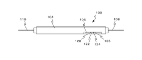
- FIG. 1 is a top view of an optical modulator according to a first embodiment of the present invention.
- 1 is a side view of an optical modulator according to a first embodiment of the present invention.
- 1 is a bottom view of an optical modulator according to a first embodiment of the present invention.
- It is a figure which shows the structure of FPC used for the optical modulator shown to FIG. 1A.
- It is a figure which shows an example of the state which connected the optical modulator shown to FIG. 1A to the circuit board in which the electronic circuit was comprised.
- It is a figure which shows an example of the state which connected the optical modulator shown to FIG. 1A to the circuit board in which the electronic circuit was comprised.
- FIG. 16A shows the structure of the optical transmission apparatus which concerns on the 2nd Embodiment of this invention. It is a top view of the conventional optical modulator. It is a side view of the conventional optical modulator. It is a bottom view of the conventional optical modulator. It is a figure which shows the structure of FPC used for the optical modulator shown in FIG. It is a figure which shows an example of the state which connected the optical modulator shown to FIG. 16A to the circuit board in which the electronic circuit was comprised. It is a figure which shows an example of the state which connected the optical modulator shown to FIG. 16A to the circuit board in which the electronic circuit was comprised. It is a figure which shows an example of a deformation
- the optical modulator 100 includes an optical modulation element 102, a housing 104 that accommodates the optical modulation element 102, a flexible wiring board (FPC) 106 that electrically connects an external circuit board, and an optical circuit that transmits light to the optical modulation element 102. , And an optical fiber 110 that guides the light output from the light modulation element 102 to the outside of the housing 104.
- FPC flexible wiring board
- the light modulation element 102 includes, for example, four Mach-Zehnder type optical waveguides formed on an LN substrate, and four high-frequency electrodes (RF electrodes) that are formed on the Mach-Zehnder type optical waveguide and modulate light waves propagating in the optical waveguide. ) DP-QPSK modulator. Two lights output from the light modulation element 102 are combined by a lens optical system including a polarization combiner, for example, and guided to the outside of the housing 104 via the optical fiber 110.
- a lens optical system including a polarization combiner, for example, and guided to the outside of the housing 104 via the optical fiber 110.
- the housing 104 includes four lead pins 120, 122, 124, 126 connected to four RF electrodes (not shown) included in the light modulation element 102.
- Lead pins 120, 122, 124, 126 provided in the housing 104 are inserted into through holes 220, 222, 224, 226 described later provided in the FPC 106, and the through holes 220, 222, 224, 226 and the lead pins 120, Between 122, 124 and 126, each is fixed by solder.
- FIG. 2 is a diagram showing the configuration of the FPC 106.
- the FPC 106 is manufactured using, for example, a polyimide-based material for a substrate (hereinafter referred to as an FPC substrate).
- the FPC 106 is configured to be rectangular in plan view.
- the shape of the FPC 1606 is generally a horizontally long rectangle in order to shorten the wiring pattern as much as possible to keep the microwave loss low.
- the FPC 106 has a rectangular shape.
- the shape of the FPC 106 is not limited to this, and may be a substantially quadrangular shape, for example.
- side refers to a rectangular side formed by the FPC 106, but when the FPC 106 is configured by a substantially quadrilateral, the “side” refers to the side of the substantially quadrilateral formed by the FPC 106. Means.
- four pads 210, 212, 214, and 216 are formed side by side along the direction of the one side 200. Further, on the side of the other side 202 facing the side 200, for example, four through holes 220, 222, 224, and 226 are formed side by side along the direction of the side 202. Further, the four pads 210, 212, 214, and 216 are electrically connected to the through holes 220, 222, 224, and 226 by wiring patterns 230, 232, 234, and 236, respectively.
- the four through holes 220, 222, 224, and 226 are connected to the four lead pins 120, 122, 124, and 126 included in the housing 104, respectively.
- pads 210, 212, 214, and 216 are connected to pads that constitute part of the circuit (for example, by soldering), high-frequency signals output from the electronic circuit are optically modulated via the FPC 106. Applied to the RF electrode of the element 102.
- the wiring patterns 230, 232, 234, and 236 formed on the FPC 106 may be configured using a known line configuration as a high-frequency signal line such as a microstrip line, a coplanar line, or a grand coplanar line.
- a ground pattern can be formed on the FPC 106 in accordance with the configuration (not shown).
- the size of the FPC 106 is, for example, the length in the long side direction (direction of the side 200) in order to keep the wiring patterns 230, 232, 234, and 236 as short as possible and suppress the microwave loss as in the conventional FPC 1606 described above.
- the length in the short side direction (direction perpendicular to the side 200) is about 10 mm or less.
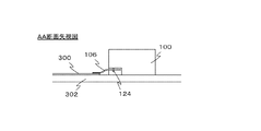
- FIG. 3A and 3B are diagrams illustrating an example of a state in which the optical modulator 100 is connected to a circuit board on which an electronic circuit is configured.
- FIG. 3A is a diagram viewed from the top surface of the optical modulator 100, and FIG. It is AA cross-sectional arrow view in FIG. 3A.
- FIG. 3B the description of the internal configuration of the optical modulator 100 is omitted.
- the optical modulator 100 and the circuit board 300 are fixed to the base 302 in the housing of the optical transmission device, for example.
- the FPC 106 of the optical modulator 100 extends from the connection portion with the lead pins 120, 122, 124, 126 to the left in the drawing, bends in the diagonally lower left direction in FIG. 3B, and pads 310, 312, Pads 210, 212, 214, 216 are soldered to 314, 316.
- the four sides of the rectangular FPC 106 are adjacent to one side 200 where the pads 210, 212, 214, and 216 are formed.
- the two sides 204 and 206 which are formed in the vicinity of the two corners 240 and 242 to which the one side 200 is connected, from a part of the sides 204 and 206 toward the inside of the FPC 106, respectively.
- the notches 250 and 252 are provided symmetrically.
- the amount of deformation of the pads 210, 212, 214, 216 of the FPC 106 with respect to the pads 310, 312, 314, 316 on the circuit board 300 is reduced and the force required for alignment is weakened, so that the alignment becomes easy.
- the positions of the pads 210, 212, 214, 216 can be accurately fixed with respect to the pads 310, 312, 314, 316. Further, since the force required to bring the pads 210, 212, 214, 216 into close contact with the pads 310, 312, 314, 316 is weakened, the pads 210, 212, 214, 216 and the pads 310, 312, 314, 316 are interposed.
- the cutouts 250 and 252 of the FPC 106 can be manufactured without requiring an additional process if a mold used for punching the FPC 106 from a sheet base material of the FPC is designed in the shape shown in FIG. Therefore, the above effect can be realized at a low cost.
- the optical modulator 100 having the above-described configuration is a pad connected to the circuit board of the FPC 106 that connects the four lead pins 120, 122, 124, 126 provided on the housing 104 and an external circuit board.
- the FPC 106 is deformed because the rectangular cutouts 250 and 252 are provided on each of the two sides 204 and 206 adjacent to the one side 200 where the 210, 212, 214, and 216 are formed.
- the stress applied to the FPC 106 and the pressing reaction force due to the stress are effectively reduced.
- the variation in solder thickness uniformity and alignment in the solder fixing step is reduced, and the variation in high-frequency characteristics of the optical modulator 100 after connection to the circuit board is effectively reduced.
- the depths of the notches 250 and 252 are portions where stress is concentrated. Therefore, it is necessary to determine that the end portion is not too close to the pads 210, 212, 214, and 216. For example, when the length of the FPC 106 in the direction of the side 200 is about 20 mm or less, the depths of the notches 250 and 252 are within a few millimeters, but sufficient effects can be exhibited even in this range.
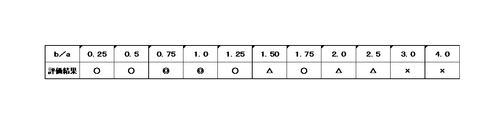
- FIG. 4 shows the solder joint uniformity and finish quality between the pads 210, 212, 214, 216 of the FPC 106 and the pads 310, 312, 314, 316 of the circuit board 300, which are realized as a result of the reaction force relaxation. Is a result of evaluation by changing the positions of the notches 250 and 252.
- the length a of the pads 210, 212, 214, and 216 used for evaluation is about 1.3 mm.
- the worst value dispersion is about 3 dB for the “ ⁇ ” evaluation, about 2 dB for the “ ⁇ ” evaluation, about 1 dB for the “ ⁇ ” evaluation, and about 0.5 dB for the “ ⁇ ” evaluation.
- Met there is a certain correlation between the result of the evaluation and the degree of high-frequency characteristic variation, and by using an FPC configuration that has obtained a good result of a certain level or more in the evaluation, the optical modulator 100 High frequency characteristic variation can be improved.
- connection uniformity / finished quality tends to decrease as the positions of the notches 250, 252 move away from the pads 210, 212, 214, 216, and b / a ⁇ 1.25. It can be seen that good quality can be obtained in the range. This tendency was the same in the evaluations performed on the pads 210, 212, 214, and 216 having the length a different from the above (about 1.3 mm).
- the notches 250 and 252 have a distance b from the side 200 where the pads 210, 212, 214 and 216 are provided to the center of the notches 250 and 252, and the length of the pads 210, 212, 214 and 216. It is desirable to provide at a position where b / a ⁇ 1.25 with respect to a.
- the effect of the reaction force relaxation is almost independent of the size (or width) of the notches 250 and 252. Accordingly, the above-described reaction force relaxation effect can be obtained even by using “cuts” formed by cutting the substrate of the FPC 106 with a predetermined length instead of the notches 250 and 252 having a finite width. .
- the notches 205 and 252 are provided symmetrically. However, the notches 205 and 252 may be provided at an asymmetric position, and it is more preferable that the asymmetric position is in a range of b / a ⁇ 1.25.
- FPCs indicate FPCs that can be used in the optical modulator 100 in place of the FPC 106.
- the rectangular cutouts 250 and 252 are provided symmetrically.
- the two sides 204 and 206 are also rectangular in the vicinity of the two corners connected to the other side 202 facing the one side 200. It is assumed that the notches are provided symmetrically.
- FIG. 5 is a diagram showing a configuration of an FPC 500 that can be used in place of the FPC 106 according to this modification. 5, the same reference numerals as those in FIG. 2 are used for the same components as those of the FPC 106 illustrated in FIG. 2, and the above description of FIG. 2 is incorporated.
- the FPC 500 shown in FIG. 5 has the same configuration as the FPC 106 shown in FIG. 2, but has two corners connected to the other side 202 facing the one side 200 where the pads 210, 212, 214, and 216 are formed ( That is, rectangular notches 510 and 512 are also provided symmetrically in the vicinity of the corners 502 and 504 at both ends of the side 202.
- the corners at both ends of the side 202 are likely to be deformed due to the manufacturing process of the FPC 106, and lead pins 120, 122, 124, It is easy to contact a part of the casing 104 when the 126 is fixed by soldering. By this contact, stress is applied to the corners at both ends of the side 202 of the FPC 106, and the stress propagates in the plane of the FPC 106 and is transmitted to the side 200 facing the side 202, thereby forming the pads 210, 212, 214, and 216. Can induce deformation in the part.
- the notches 510 and 512 are also formed in the vicinity of both end corners 502 and 504 of the side 202 in contact with the housing 104, so that the stress applied by the contact is released by the notches 510 and 512.
- the deformation of the pads 210, 212, 214, and 216 can be effectively prevented.
- the FPC 500 is cut by a predetermined length at the notches 510 and 512. It is also possible to make a notch constructed.
- rectangular cutouts are arranged symmetrically in the vicinity of the corners 240 and 242 of the one side 200, respectively.
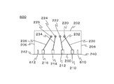
- FIG. 6 is a diagram showing a configuration of an FPC 600 that can be used in place of the FPC 106 according to this modification. 6, the same reference numerals as those in FIG. 2 are used for the same components as those of the FPC 106 illustrated in FIG. 2, and the above description of FIG. 2 is incorporated.
- the FPC 600 shown in FIG. 6 has the same configuration as the FPC 106 shown in FIG. 2, but two corners (one corner 200 where the pads 210, 212, 214, and 216 are formed) connected to the one side 200 ( That is, rectangular cutouts 610 and 612 are provided substantially parallel to the length direction of the pads 210, 212, 214, and 216 in the vicinity of the corners 240 and 242 at both ends of the side 200.
- the notches 610 and 612 are provided on one side 200 where the pads 210, 212, 214 and 216 are formed. Therefore, the pads 210, 212, 214 and 216 and the through holes 220, 222, 224 and 226 are provided. It is possible to secure a wide area for forming the wiring patterns 230, 232, 234, and 236 connecting the two.
- the FPC 600 is cut by a predetermined length at the notches 610 and 612. It is also possible to make a notch constructed.
- a notch constituted by a curve is arranged at a position on the two sides 204 and 206 that is not near the corners 240 and 242.
- This modification is an alternative to the FPC 106 in the case where the notches 250 and 252 cannot be provided near the corners 240 and 242 in the vicinity of 240 and 242, for example, because of the FPC board holding method of the assembly jig. It can be used as a configuration.
- FIG. 7 is a diagram showing a configuration of an FPC 700 that can be used in place of the FPC 106 according to this modification.
- the same reference numerals as those in FIG. 2 are used for the same components as those of the FPC 106 shown in FIG. 2, and the above description of FIG.
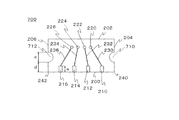
- the FPC 700 shown in FIG. 7 has the same configuration as the FPC 106 shown in FIG. 2, but instead of the notches 250 and 252 having a rectangular shape provided in the vicinity of the corners 240 and 242, Notches 710 and 712 having a shape notched along a predetermined curve are arranged in a distant portion (a portion not near the vicinity), and the shape of the FPC 700 in a plan view is constricted.
- notches 710, 712 are provided not at the corners 240, 242 near the pads 210, 212, 214, 216 but at positions away from the corners 240, 242. 712 has a wide opening. As a result, the stress generated in the corner portions 240 and 242 is released in a wide range at the sides 204 and 206, so that the deformation of the FPC 700 is suppressed. Further, since the notches 710 and 712 are configured with curves and do not have a bent portion, stress is not concentrated on a part of the edges of the notches 710 and 712, and the stress is dispersed on an average. Can do.
- the shapes of the notches 710 and 712 can be various shapes such as a semicircular shape, a semi-elliptical shape, and a combination of an arc and a straight line.
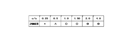
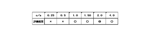
- FIGS. 8A and 8B show the positions between the pads 210, 212, 214, and 216 of the FPC 700 and the pads 310, 312, 314, and 316 of the circuit board 300 when the notches 710 and 712 are arranged at two different positions. It is the result of having evaluated the uniformity and finish quality of a solder connection part, changing the magnitude
- a parameter c / a obtained by normalizing the width c of the notches 710 and 712 shown in FIG. 7 by the lengths (distances in the vertical direction in the drawing) a of the pads 210, 212, 214, and 216 is used.
- the uniformity and finished quality of the solder joints for various values of c / a were evaluated.
- the evaluation criteria are the same as the evaluation criteria for evaluation in FIG. 4 described above.
- FIG. 8A shows the end point (notch) closer to the side 200 among the end points of the notches 710 and 712 between the lengths of the pads 210, 212, 214 and 216 (distance in the vertical direction in FIG. 7) a.
- the lengths a of the pads 210, 212, 214, and 216 are all about 1.3 mm.
- the notches 250 and 252 of the FPC 106 shown in FIG. 2 generate a reaction force when the deformation that occurs in the FPC 106 in the manufacturing process of the FPC 106 presses the pads 210, 212, 214, and 216 against the circuit board, for example. This is to alleviate this.
- the FPC generated in the assembly process of the optical modulator 100 such as the process of inserting the lead pins 120, 122, 124, and 126 into the through holes 220, 222, 224, and 226 and fixing them with solder.
- An object of the present invention is to effectively suppress the deformation.
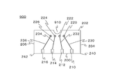
- FIG. 9 is a diagram illustrating a configuration of an FPC 900 that can be used in place of the FPC 106 according to the present modification. 9, the same reference numerals as those in FIG. 2 are used for the same components as those of the FPC 106 illustrated in FIG. 2, and the above description of FIG. 2 is incorporated.
- the FPC 900 shown in FIG. 9 has the same configuration as the FPC 106 shown in FIG. 2, but does not have the rectangular cutouts 250 and 252, and one side 200 on which the pads 210, 212, 214, and 216 are formed.
- a notch 910 formed of a curve is provided at a substantially central portion of the side 202 on the side where the through holes 220, 222, 224, and 226 facing each other are formed.
- the deformation of the FPC that occurs in the assembly process of the optical modulator 100 is mainly: Difference in thermal expansion coefficient between the lead pins 120, 122, 124, 126 and the FPC due to heat generated when the solder is fixed between the lead pins 120, 122, 124, 126 and the through holes 220, 222, 224, 226.
- Difference in thermal expansion coefficient between the lead pins 120, 122, 124, 126 and the FPC due to heat generated when the solder is fixed between the lead pins 120, 122, 124, 126 and the through holes 220, 222, 224, 226.
- the lead pins 120, 122, 124, 126 are inserted into the through holes 220, 222, 224, 226, due to rubbing between the lead pins 120, 122, 124, 126 and the through holes 220, 222, 224, 226, etc.
- the FPC 900 of this modification has a notch 910 in the side 202 on the side where the through holes 220, 222, 224, and 226 are formed, the above-described stress that may occur in the assembly process of the optical modulator 100 is released, Deformation of the FPC 900 due to the stress can be effectively prevented. As a result, the deformation (or distortion) is prevented from propagating to the side 200, and in the soldering connection between the pads 210, 212, 214, 216 and the pads 310, 312, 314, 316 of the circuit board 300. Good connection uniformity and finished quality can be obtained, and variations in the high-frequency characteristics of the signal path from the circuit board 300 to the optical modulator 100 can be effectively and inexpensively reduced.
- the notch 910 is shown as being semicircular.
- the shape of the notch 910 is not limited to this, and may be various curved shapes such as a semi-elliptical shape and a combination of an arc and a straight line. be able to.
- the stress associated with the FPC is reduced to reduce the FPC at the time of the positioning.
- the purpose is to reduce or prevent deformation.
- FIG. 10 is a diagram showing a configuration of an FPC 1000 that can be used in place of the FPC 106 according to this modification. 10, the same reference numerals as those in FIG. 2 are used for the same components as those of the FPC 106 illustrated in FIG. 2, and the above description of FIG. 2 is incorporated.
- the FPC 1000 illustrated in FIG. 10 has the same configuration as the FPC 106 illustrated in FIG. 2, but does not have the notches 250 and 252 and is a through surface facing the one side 200 where the pads 210, 212, 214, and 216 are formed.
- the FPC When positioning the FPC by bringing one side of the FPC into contact with a predetermined portion of the housing 104 of the optical modulator 100, the FPC is deformed into corners corresponding to the one side or both ends of the one side (for example, FPC If there is a manufacturing process), the deformation is promoted by the contact with the housing 104 (that is, the deformation becomes large). For this reason, the stress or strain generated in the FPC due to the deformation propagates to other sides, so that the adhesion between the pad formed on the FPC and the pad of the external circuit board is reduced, and the solder connection between these pads is performed. The uniformity of the can deteriorate.
- the side 202 where the through holes 220, 222, 224, 226 facing the side 202 (that is, the side 200 where the pads 210, 212, 214, 216 are formed) is formed.
- Side 202) and two sides 204 and 206 adjacent to the side 202 are connected by curved portions 1010 and 1012 having a predetermined radius of curvature, and corners are provided at both ends of the side 202.
- the suppression effect on the propagation of stress or strain caused by contact with the housing 104 as described above is a curve that connects the side 202 that is in contact with the housing 104 and the sides 204 and 206 that are adjacent to the side 202.
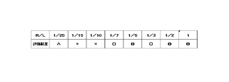
- FIG. 11 shows the uniformity and finish quality of the solder joints between the pads 210, 212, 214, 216 of the FPC 1000 and the pads 310, 312, 314, 316 of the circuit board 300, and the radius of curvature of the curved portions 1010, 1012. It is the result of changing and evaluating.
- R / L was used to evaluate the uniformity and finished quality of the solder joint for various values of R / L.
- the evaluation criteria are the same as the evaluation criteria for evaluation in FIG. 4 described above.
- the radius of curvature R of the curved portions 1010 and 1012 is preferably R ⁇ L / 7 in order to obtain good solder connection uniformity and finished quality.
- L is 10 mm (as described above, the general short side length of the optical modulator FPC is about 10 mm or less)
- the curvature radius R of the curved portions 1010 and 1012 is about 1.4 mm. It is desirable.
- the curved portions 1010 and 1012 are indicated by arcs.
- the shape of the curved portions 1010 and 1012 is not limited to this, and may be an ellipse or other arbitrary curve as long as it has a predetermined radius of curvature. Can be.
- a sixth modification of the FPC 106 used in the optical modulator 100 shown in FIG. 1A will be described.
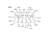
- FIG. 12 is a diagram showing a configuration of an FPC 1200 that can be used in place of the FPC 106 according to this modification. 12, the same reference numerals as those in FIG. 2 are used for the same components as those of the FPC 106 shown in FIG. 2, and the above description of FIG. 2 is incorporated.
- the FPC 1200 shown in FIG. 12 has the same configuration as the FPC 106 shown in FIG. 2, but instead of the notches 250 and 252 provided in the vicinity of the corners 240 and 242, a part (near the vicinity) of the corners 240 and 242.
- Notch portions 1210 and 1212 having a shape cut out along a predetermined curve are arranged in a portion that is not, and the shape of the FPC 1200 in a plan view is constricted.
- the side 202 on the side where the through holes 220, 222, 224, 226 facing the one side 200 on which the pads 210, 212, 214, 216 are formed, and two sides adjacent to the side 202 are provided.
- 204 and 206 are connected by curved portions 1220 and 1222 having a predetermined radius of curvature.
- This modification is a combination of the notches 710 and 712 (FIG. 7) of the FPC 700 according to the third modification and the curved portions 1010 and 1012 (FIG. 10) of the FPC 1000 according to the fifth modification. is there.
- notches 1210 and 1212 are formed in portions not in the vicinity of the pads 210, 212, 214, and 216, and the deformation of the FPC 1200 due to contact with the housing 104 by the curved portions 1220 and 1222 and Suppress or prevent distortion propagation.
- a seventh modification of the FPC 106 used in the optical modulator 100 shown in FIG. 1A will be described.
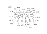
- FIG. 13 is a diagram showing a configuration of an FPC 1300 that can be used in place of the FPC 106 according to this modification. Note that in FIG. 13, the same reference numerals as those in FIG. 2 are used for the same components as those of the FPC 106 shown in FIG. 2, and the above description of FIG.
- the FPC 1300 illustrated in FIG. 13 has the same configuration as the FPC 106 illustrated in FIG. 2, but instead of the notches 250 and 252 provided in the vicinity of the corner portions 240 and 242, a portion (near the vicinity) of the corner portions 240 and 242.
- Notch portions are provided with notches 1310 and 1312 having a shape that is notched along a predetermined curve, and the FPC 1300 has a constricted shape in plan view.
- a curved line is formed at a substantially central portion of the side 202 on the side where the through holes 220, 222, 224, and 226 facing the one side 200 on which the pads 210, 212, 214, and 216 are formed.
- a notch 1320 is provided.
- the side 202 and the two sides 204 and 206 adjacent to the side 202 are connected by curved portions 1330 and 1332 having a predetermined radius of curvature.
- This modification relates to notches 710 and 712 (FIG. 7) of the FPC 700 according to the third modification, a notch 910 (FIG. 9) of the FPC 900 according to the fourth modification, and a fifth modification.
- the curved portions 1010 and 1012 (FIG. 10) of the FPC 1000 are combined, and notches 1310 and 1312 are formed in portions that are not in the vicinity of the pads 210, 212, 214, and 216.
- a notch 1320 is formed on the side 202 on the side where the through holes 220, 222, 224, 226 are formed, and the connection between the through holes 220, 222, 224, 226 and the lead pins 120, 122, 124, 126 is performed.
- Deformation of the FPC 1300 that may occur in the process is suppressed or reduced. Further, the curved portions 1330 and 1332 prevent the FPC 1300 from being deformed and the propagation of the distortion due to the contact between the side 202 and the housing 104.
- the modified examples shown in FIGS. 9, 10, 12, and 13 described above particularly have through holes 220, 222, 224, facing one side 200 where the pads 210, 212, 214, and 216 are formed.
- 14 shows a state in which, for example, the side 202 of the FPC 1300 shown in FIG.
- the through holes 220, 222, 224, 226 and the lead pins 120, 122, 124, 126 are fixed by soldering.
- An example is shown. 9, 10, and 12 are similar to the FPC 1300 shown in FIG. 14, and the through holes 220, 222, 224, and 226 are arranged in a state where the side 202 is positioned in contact with the housing 104.
- the lead pins 120, 122, 124, 126 can be soldered.
- the curved portions 1010 and 1012, 1210 and 1212, and 1330 and 1332 in the modified examples shown in FIGS. 10, 12, and 13 are stresses generated by the side 202 coming into contact with the housing 104 or Since distortion is reduced or relaxed (suppressed), the casing 104 is processed so as to have a curve similar to these curved sections, and the curved section 1010 or the like is brought into contact with the casing 104 having the curve. Note that it doesn't make sense.
- the present embodiment is an optical transmission device on which the optical modulator 100 (including any modification shown in FIGS. 5 to 13) shown in the first embodiment is mounted.
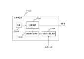
- FIG. 15 is a diagram illustrating a configuration of the optical transmission apparatus according to the present embodiment.
- the optical transmission device 1500 includes an optical modulator 1502, a light source 1504 that makes light incident on the optical modulator 1502, a modulation signal generation unit 1506, and a modulation data generation unit 1508.
- the optical modulator 1502 is an optical modulator 100 shown in FIG. 1A (in place of the FPC 106, one of the FPCs 500, 600, 700, 1000, 1200, or 1300 shown in FIGS. 5 to 7, 9, 10, 12, and 13 is used. It may be provided).
- the modulation data generation unit 1508 receives transmission data given from the outside, generates modulation data for transmitting the transmission data (for example, data obtained by converting or processing transmission data into a predetermined data format), and The generated modulation data is output to modulation signal generation section 1506.
- the modulation signal generation unit 1506 is an electronic circuit that generates an electric signal for causing the optical modulator 1502 to perform a modulation operation. Based on the modulation data output from the modulation data generation unit 1508, the modulation signal generation unit 1506 supplies the modulation data to the optical modulator 1502.
- a modulation signal which is a high-frequency signal for performing an optical modulation operation according to the above, is generated and input to the optical modulator 100.
- the modulation signals are four RF signals corresponding to the four RF electrodes (not shown) of the light modulation element 102 included in the light modulator 100.
- the four RF signals are respectively input to pads 210, 212, 214, and 216 of the FPC 106 of the optical modulator 100 (which may be any of the above-described modifications of the FPC 106 as described above), and the wiring pattern 230, 232, 234 and 236, through holes 220, 222, 224 and 226, and lead pins 120, 122, 124 and 126, respectively, are applied to the RF electrodes.
- the light output from the light source 1504 is modulated by the optical modulator 100 and is output from the optical transmission device 1500 as modulated light.
- each signal line of four RF signals output from the modulation signal generation unit 1506 and the pad 210 of the FPC 106 provided in the optical modulator 100. , 212, 214, and 216 can be made uniform in connection and finished quality. As a result, it is possible to effectively and inexpensively reduce the variation in the high-frequency characteristics (reflection characteristics, etc.) of the signal path between the signal line and the RF electrode of the light modulation element 102 included in the light modulator 100, and to obtain good characteristics. It becomes possible to mass-produce the optical transmitter having the same stably.
- an optical modulator including an optical modulation element having four RF electrodes using LN as a substrate is shown.
- the present invention is not limited to this, and a number of RFs other than four is provided.
- the present invention can be similarly applied to an optical modulator having an electrode and / or an optical modulator using a material other than LN as a substrate.
- the configuration of the FPC 106 shown in FIG. 2 and the configuration of the modified example of the FPC 106 shown in FIGS. 5 to 13 can be used not only as individual FPCs, but also combined into one FPC. It can also be configured and used.
- Lead pin 200, 202, 204, 206, 1700, 1702 ... Side, 210, 212, 214, 216, 310, 312, 314, 316, 1710, 1712, 1714, 1716, 1810, 1812, 1814, 1816 ...
Landscapes
- Physics & Mathematics (AREA)
- Nonlinear Science (AREA)
- Engineering & Computer Science (AREA)
- Microelectronics & Electronic Packaging (AREA)
- General Physics & Mathematics (AREA)
- Optics & Photonics (AREA)
- Chemical & Material Sciences (AREA)
- Ceramic Engineering (AREA)
- Crystallography & Structural Chemistry (AREA)
- Electromagnetism (AREA)
- Optical Modulation, Optical Deflection, Nonlinear Optics, Optical Demodulation, Optical Logic Elements (AREA)
- Structure Of Printed Boards (AREA)
Abstract
外部の回路基板との電気的接続を行うFPCを備えた光変調器において、当該回路基板から光変調器に至る信号経路の高周波特性のばらつきを、効果的且つ安価に低減すること。 回路基板との間の電気的接続を行うフレキシブル配線板(106)を備えた光変調器(100)である。前記フレキシブル配線板は略四辺形を為し、前記フレキシブル配線板には、前記略四辺形の一の辺(200)に沿って前記回路基板と電気的に接続されるパッド(210等)が形成されている。また、前記フレキシブル配線板は、当該フレキシブル配線板の辺又は端部に加わる機械的応力を開放し及び又は当該辺又は端部に発生した歪の伝搬を防止するための、少なくとも一つの辺の一部から前記フレキシブル配線板の内部方向に向かって設けられた切り込み又は切り欠き(250等)を有し、及び又は少なくとも2つの隣接する辺をつなぐ曲線部(1010等)が設けられている。
Description
本発明は、光変調器及び光送信装置に関し、特に、高周波信号を入力するためのFPC(Flexible Printed Circuits、フレキシブル配線板)を備える光変調器、及びそれを用いた光送信装置に関する。
高速/大容量光ファイバ通信システムにおいては、導波路型の光変調素子を組み込んだ光変調器が多く用いられている。中でも、電気光学効果を有するLiNbO3(以下、LNともいう)を基板に用いた光変調素子は、光の損失が少なく且つ広帯域な光変調特性を実現し得ることから、高速/大容量光ファイバ通信システムに広く用いられている。
このLNを用いた光変調素子では、マッハツェンダ型光導波路と、当該導波路に変調信号である高周波信号を印加するためのRF電極と、当該導波路における変調特性を良好に保つため種々の調整を行うためのバイアス電極と、が形成されている。そして、光変調素子に形成されたこれらの電極は、当該光変調素子を備える光変調器の筺体に設けられたリードピンやコネクタを介して、外部の電子回路に接続される。
一方、光ファイバ通信システムにおける変調方式は、近年の伝送容量の増大化の流れを受け、QPSK(Quadrature Phase Shift Keying)やDP-QPSK(Dual Polarization - Quadrature Phase Shift Keying)等、多値変調や、多値変調に偏波多重を取り入れた伝送フォーマットが主流となっている。
QPSK変調を行う光変調器(QPSK変調器)やDP-QPSK変調を行う光変調器(DP-QPSK変調器)は、ネスト型マッハツェンダ型光導波路を備え、複数の高周波信号電極及び複数のバイアス電極を備えることから(例えば、特許文献1参照)、デバイスサイズが増大化する傾向があり、特に小型化の要請が強い。
この小型化の要請に対応する一つの策として、従来、RF電極と外部の電子回路とを接続するインタフェースとして光変調器の筺体に設けられていたプッシュオン型の同軸コネクタを、バイアス電極のインタフェースと同様のリードピンに置き換え、これらのリードピンを外部の回路基板に接続するためのFPC(フレキシブル配線板(FPC:Flexible Printed Circuits)を付加した光変調器が実現されている。
例えば、DP-QPSK変調器では、それぞれにRF電極を有する4つのマッハツェンダ型光導波路で構成される光変調素子が用いられる。この場合、光変調器筺体に4つのプッシュオン型同軸コネクタを設けたのでは筺体の大型化は避けられないが、同軸コネクタに代えてリードピンとFPCとを用いれば、小型化が可能となる。
また、光変調器筺体のリードピンと、当該光変調器に変調動作を行わせるための電子回路が搭載された回路基板と、の間が、上記FPCを介して接続されるので、従来用いていた同軸ケーブルを用いる必要が無く当該同軸ケーブルの余長処理に必要であったスペースが不要となり、光送信装置内における光変調器の実装スペースを縮小することができる。
光変調器に用いられるFPCは、例えば可撓性のあるポリイミドベースの材料を基板(以下、FPC基板)として用いて作製され、一方の端部付近に形成された複数のスルーホールは、他方の端部に形成された同数のパッドと電気的に接続されている。そして、光変調器筺体の底面又は側面から突き出た複数のリードピンが上記複数のスルーホールにそれぞれ挿通されてハンダ固定される。また、上記複数のパッドは、回路基板にそれぞれハンダ固定される。これにより、当該回路基板上のパッドから与えられる高周波信号が、それぞれ対応する上記スルーホールとリードピンとを介して、光変調素子の対応するRF電極に与えられて、高速光変調が行われる。
上記のFPCを用いた光変調器では、上述のように、筺体を小型化することができ、回路基板上における光変調器の実装スペースも縮小することができるので、光伝送装置の小型化に大きく貢献し得る。
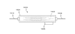
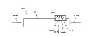
図16A、図16B、図16Cは、そのようなFPCを備える従来の光変調器の構成を示す図であり、図16Aは光変調器の上面図、図16Bは正面図、図16Cは底面図である。この光変調器1600は、光変調素子1602と、光変調素子1602を収容する筺体1604と、フレキシブル配線板(FPC)1606と、光変調素子1602に光を入射するための光ファイバ1608と、光変調素子1602から出力される光を筺体1604の外部へ導く光ファイバ1610と、を備える。
筺体1604には、光変調素子1602の4つのRF電極(不図示)にそれぞれ接続された4つのリードピン1620、1622、1624、1626が設けられており、当該リードピン1620、1622、1624、1626は、FPC1606に設けられた後述するスルーホール1720、1722、1724、1726に挿通されてハンダにより固定されている。
図17は、FPC1606の構成を示す図である。FPC1606は、図示下側の一の辺1700の近傍に、当該一の辺1700の方向に沿って4つのパッド1710、1712、1714、1716が並んで形成されている。また、辺1700に対向する他の辺1702の側には、例えば辺1702の方向に沿って、4つのスルーホール1720、1722、1724、1726が並んで形成されている。さらに、4つのパッド1710、1712、1714、1716は、それぞれ、配線パターン1730、1732、1734、1736によりスルーホール1720、1722、1724、1726に電気的に接続されている。
そして、4つのパッド1710、1712、1714、1716が外部の回路基板のパッドに対してそれぞれハンダ付けされることにより、光変調器1600が備える光変調素子1602のRF電極と当該回路基板上に構成された電子回路とが電気接続に実装される。なお、FPC1606の形状は、配線パターンを極力短くしてマイクロ波損失を低く抑えるべく、図示のように信号伝送方向に短い辺を持つ横長の長方形になるのが一般的であり、図示の例のように4つのパッド1710、1712、1714、1716を持つ場合には、長辺方向で約20mm以下、短辺方向で約10mm以下の長方形となる。
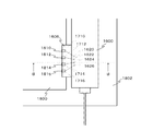
図18A、図18Bは、電子回路が構成された回路基板に光変調器1600を接続した状態の一例を示す図であり、図18Aは光変調器1600の上面方向から見た図、図18Bは図18AにおけるBB断面矢視図である。なお、図18Bにおいて光変調器1600の内部の構成については記載を省略している。
光変調器1600と回路基板1800とは、例えば光送信装置の筺体内のベース1802に固定されている。光変調器1600のFPC1606は、リードピン1620、1622、1624、1626との接続部分から図示左方へ延在し、図18Bの図示斜め左下方向に曲がって、FPC1606のパッド1710、1712、1714、1716が回路基板1800上のパッド1810、1812、1814、1816にハンダ付けされる。
しかしながら、上記のようなFPC付き光変調器を回路基板に接続して光送信装置を構成すると、FPC1606の製造時に発生し得る当該FPC1606の変形や、当該FPC1606と光変調器筺体1604のリードピン1620、1622、1624、1626との間のハンダ付けに際して発生し得る当該FPC1606の反りや伸び等の様々な変形に起因して、FPC1606上のパッド(FPCパッド)1710、1712、1714、1716と回路基板1800上のパッド(回路基板パッド)1810、1812、1814、1816との間の接続状態に僅かなばらつき(介在するハンダの厚さのばらつきや厚さの均一性のばらつき、あるいはFPCパッドと回路基板パッドとの間の位置ずれのばらつき)が生じ得る。
図19は、変形したFPCの一例を示す図である。図示の例では、FPC1900は、基板角部において図示上方向へ変形している。この変形は、FPCの製造工程に起因する変形としてよくみられる。FPCは、例えばポリイミド基板上に銅(Cu)や金(Au)等で形成された配線パターンを備え、それらの配線パターンを保護するための保護膜なども形成されている。個々のFPCは、例えば一のFPCを構成する配線パターンをFPC基板のシート状母材にマトリックス状に繰り返し多数形成し、当該シート状母材から、それぞれが一のFPCを構成する部分を打ち抜くことで製造される。図示のような角部における変形は、個々のFPCが上記のような打ち抜きによって量産製造されることに由来していると考えられる。
ただし、製造時に発生するFPCの変形は、当該FPCの製造プロセスにおける様々な要因で発生し、当該変形の度合いは、材料ロットや製造ロットなどの要因で変化し得るものであり、変形の形状も、反り、うねり、伸びなど様々であって、これらを制御し、抑制することは困難である。
更に、このようなFPCの変形は、製造プロセスによって発生するだけでなく、FPCを光変調器筺体のリードピンに半田固定する際の熱や、光変調器を光送信装置内に組み込む際にFPCに加わる応力、あるいは光変調器を回路基板上へ実装する際にFPCに加わる応力によっても発生する。
特に、光変調器においては、FPCに伝搬させる高周波信号は数十GHzというマイクロ波領域に達していることから、上述した接続状態の僅かなばらつきに起因して、回路基板パッドからリードピンに至るまでの高周波信号経路の反射特性や伝送特性に大きなばらつきが生じ得る。その結果、光変調器における光変調特性を良好に保って所望の光伝送品質が確保することが困難となる事態が生じ得る。
また、この問題は、光変調器の小型化の要請からFPCパッドができる限り微小なサイズで構成されることから、FPCの製造工程(例えば基板打ち抜き工程)においてFPC基板に加わる応力等により当該FPCに変形を生じやすいこと、及びFPCパッドが微小であるため回路基板とのハンダ付けの際に位置ずれを生じ易いこと、等により比較的容易に発生し得る。
このような問題を解決する技術として、従来、特にFPC基板がその自重によりU字状に変形することに起因する上記問題を解決すべく、FPCが逆U字状に変形するように当該FPCが当接する筺体の一部に隆起部を設けた光モジュールが知られている(特許文献1)。
しかしながら、FPCを逆U字状に変形させても、光変調器筺体のリードピンとFPCとの間のハンダ付け組立工程において発生し得る当該FPCの反りや伸び等の様々な変形や、FPC自身の製造時における変形を一定状態に管理することは困難である。また、筺体の一部に設ける隆起部の加工ばらつきに起因して、FPCを当該隆起部に当接させたときのFPCの変形ばらつきも生じ得ることとなり得る。したがって、上記従来の技術では、上述した種々の製造ばらつきを低減して光変調器の光変調特性を良好に保つには限界がある。さらに、上記従来の技術では、筺体の一部に隆起部を設けるための加工工程が必要となることから製造コストも増加する。
上記背景より、外部の回路基板との電気的接続を行うFPCを備えた光変調器において、当該回路基板から光変調器に至る信号経路の高周波特性のばらつきを、効果的且つ安価に低減することが望まれている。
本発明の一の態様は、回路基板との間の電気的接続を行うフレキシブル配線板を備えた光変調器であって、前記フレキシブル配線板は略四辺形を為し、前記フレキシブル配線板には、前記略四辺形の一の辺に沿って前記回路基板と電気的に接続されるパッドが形成されており、前記フレキシブル配線板は、当該フレキシブル配線板の辺又は端部に加わる機械的応力を開放し及び又は当該辺又は端部に発生した歪の伝搬を防止するための、少なくとも一つの辺の一部から前記フレキシブル配線板の内部方向に向かって設けられた切り込み又は切り欠きを有し、及び又は少なくとも2つの隣接する辺をつなぐ曲線部が設けられている。
本発明の他の態様によると、前記切り込み又は切り欠きは、前記略四辺形を構成する辺のうち、前記パッドが形成された前記一の辺に隣接する2つの辺のぞれぞれの一部からそれぞれ設けられている。
本発明の他の態様によると、前記パッドは、前記一の辺から距離aの位置まで形成されており、前記切り込み又は切り欠きは、前記の一の辺からの距離1.25×a以内の位置に形成されている。
本発明の他の態様によると、前記切り込み又は前記切り欠きは、前記一の辺に対し略平行な方向に設けられている。
本発明の他の態様によると、前記切り込み又は切り欠きは、前記パッドが形成されている部分を挟む前記一の辺上の2つの位置に、当該一の辺に対して略垂直方向に形成されている。
本発明の他の態様によると、前記切り欠きは、前記フレキシブル配線板を所定の曲線に沿って切り取った形状で形成されている。
本発明の他の態様によると、前記パッドは、前記一の辺から距離aの位置まで形成されており、前記切り欠きが設けられている辺における当該切り欠きの開口部の長さcと、前記一の辺から前記開口部の近端までの距離dとが、前記距離aに対し、a≦d、及びa≦cの関係を有するように前記切り欠きが設けられている。
本発明の他の態様によると、前記切り欠きは、前記略四辺形を構成する辺のうち、前記パッドが形成された前記一の辺に対向する辺に配されており、当該切り欠きは、前記フレキシブル配線板を所定の曲線に沿って切り取った形状で形成されている。
本発明の他の態様によると、前記曲線部は、前記略四辺形を構成する辺のうち、前記パッドが形成された前記一の辺に対向する辺と、当該対向する辺に隣接する2つの辺とをそれぞれつなぐ部分に設けられている。
本発明の他の態様によると、前記曲線部は、前記パッドが形成された前記一の辺と前記対向する辺との距離Lに対し、R≧L/7の関係を満たす曲率半径Rを持つ。
本発明の他の態様によると、前記略四辺形を構成する辺のうち、前記パッドが形成された前記一の辺に隣接する2つの辺のぞれぞれの一部からそれぞれ設けられた切り欠きを有し、当該切り欠きは、前記フレキシブル配線板を所定の曲線に沿って切り取った形状で形成されている。
本発明の他の態様によると、前記略四辺形を構成する辺のうち、前記パッドが形成された前記一の辺に対向する辺に少なくとも一つの切り欠きが設けられており、当該切り欠きは、前記フレキシブル配線板を所定の曲線に沿って切り取った形状で形成されている。
本発明の他の態様は、上記いずれかの光変調器と、当該光変調器に変調動作を行わせるための電気信号を発生する電子回路と、を備える光送信装置である。
本発明の他の態様によると、前記切り込み又は切り欠きは、前記略四辺形を構成する辺のうち、前記パッドが形成された前記一の辺に隣接する2つの辺のぞれぞれの一部からそれぞれ設けられている。
本発明の他の態様によると、前記パッドは、前記一の辺から距離aの位置まで形成されており、前記切り込み又は切り欠きは、前記の一の辺からの距離1.25×a以内の位置に形成されている。
本発明の他の態様によると、前記切り込み又は前記切り欠きは、前記一の辺に対し略平行な方向に設けられている。
本発明の他の態様によると、前記切り込み又は切り欠きは、前記パッドが形成されている部分を挟む前記一の辺上の2つの位置に、当該一の辺に対して略垂直方向に形成されている。
本発明の他の態様によると、前記切り欠きは、前記フレキシブル配線板を所定の曲線に沿って切り取った形状で形成されている。
本発明の他の態様によると、前記パッドは、前記一の辺から距離aの位置まで形成されており、前記切り欠きが設けられている辺における当該切り欠きの開口部の長さcと、前記一の辺から前記開口部の近端までの距離dとが、前記距離aに対し、a≦d、及びa≦cの関係を有するように前記切り欠きが設けられている。
本発明の他の態様によると、前記切り欠きは、前記略四辺形を構成する辺のうち、前記パッドが形成された前記一の辺に対向する辺に配されており、当該切り欠きは、前記フレキシブル配線板を所定の曲線に沿って切り取った形状で形成されている。
本発明の他の態様によると、前記曲線部は、前記略四辺形を構成する辺のうち、前記パッドが形成された前記一の辺に対向する辺と、当該対向する辺に隣接する2つの辺とをそれぞれつなぐ部分に設けられている。
本発明の他の態様によると、前記曲線部は、前記パッドが形成された前記一の辺と前記対向する辺との距離Lに対し、R≧L/7の関係を満たす曲率半径Rを持つ。
本発明の他の態様によると、前記略四辺形を構成する辺のうち、前記パッドが形成された前記一の辺に隣接する2つの辺のぞれぞれの一部からそれぞれ設けられた切り欠きを有し、当該切り欠きは、前記フレキシブル配線板を所定の曲線に沿って切り取った形状で形成されている。
本発明の他の態様によると、前記略四辺形を構成する辺のうち、前記パッドが形成された前記一の辺に対向する辺に少なくとも一つの切り欠きが設けられており、当該切り欠きは、前記フレキシブル配線板を所定の曲線に沿って切り取った形状で形成されている。
本発明の他の態様は、上記いずれかの光変調器と、当該光変調器に変調動作を行わせるための電気信号を発生する電子回路と、を備える光送信装置である。
以下、図面を参照して、本発明の実施の形態を説明する。
<第1実施形態>
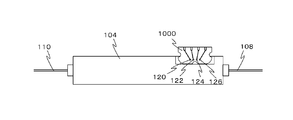
図1A、図1B、図1Cは、本発明の第1の実施形態に係る光変調器の構成を示す図である。本光変調器100は、光変調素子102と、光変調素子102を収容する筺体104と、外部の回路基板との電気的接続を行うフレキシブル配線板(FPC)106と、光変調素子102に光を入射するための光ファイバ108と、光変調素子102から出力される光を筺体104の外部へ導く光ファイバ110と、を備える。
<第1実施形態>
図1A、図1B、図1Cは、本発明の第1の実施形態に係る光変調器の構成を示す図である。本光変調器100は、光変調素子102と、光変調素子102を収容する筺体104と、外部の回路基板との電気的接続を行うフレキシブル配線板(FPC)106と、光変調素子102に光を入射するための光ファイバ108と、光変調素子102から出力される光を筺体104の外部へ導く光ファイバ110と、を備える。
光変調素子102は、例えばLN基板上に形成された4つのマッハツェンダ型光導波路と、当該マッハツェンダ型光導波路上にそれぞれ形成されて光導波路内を伝搬する光波を変調する4つの高周波電極(RF電極)を備えたDP―QPSK変調器である。光変調素子102から出力される2つの光は、例えば偏波合成器を含むレンズ光学系により偏波合成され、光ファイバ110を介して筺体104の外部へ導かれる。
筺体104は、上記光変調素子102が備える4つのRF電極(不図示)のそれぞれに接続された4つのリードピン120、122、124、126を備える。筺体104に設けられたリードピン120、122、124、126は、FPC106に設けられた後述するスルーホール220、222、224、226に挿通され、当該スルーホール220、222、224、226とリードピン120、122、124、126との間がそれぞれハンダにより固定されている。
図2は、FPC106の構成を示す図である。FPC106は、例えばポリイミドベースの材料を基板(以下、FPC基板)に用いて作製されている。FPC106は、例えば平面視が矩形に構成されている。上述したように、FPC1606の形状は、配線パターンを極力短くしてマイクロ波損失を低く抑えるべく、横長の長方形になるのが一般的である。このため、本実施形態では、FPC106は矩形形状を為すものとしている。ただし、FPC106の形状は、これに限らず、例えば略四辺形の形状を為すものとすることができる。以下の記載において、「辺」というときは、FPC106が為す矩形の辺をいうが、FPC106が略四辺形で構成される場合には、「辺」とは、FPC106が為す当該略四辺形の辺を意味する。
FPC106の図示下側の一の辺200の近傍には、当該一の辺200の方向に沿って4つのパッド210、212、214、216が並んで形成されている。また、辺200に対向する他の辺202の側には、例えば辺202の方向に沿って、4つのスルーホール220、222、224、226が並んで形成されている。さらに、4つのパッド210、212、214、216は、それぞれ、配線パターン230、232、234、236によりスルーホール220、222、224、226に電気的に接続されている。
上述のように、4つのスルーホール220、222、224、226は、それぞれ、筺体104が備える4つのリードピン120、122、124、126に接続されているので、外部の回路基板に設けられた電子回路の一部を構成するパッドに対して(例えばハンダ付けにより)パッド210、212、214、216がそれぞれ接続されることにより、当該電子回路から出力される高周波信号が、FPC106を介して光変調素子102のRF電極に印加される。
FPC106に形成される配線パターン230、232、234、236は、マイクロストリップ線路、コプレーナ線路、グランデットコプレーナ線路など、高周波用の信号線路として公知の線路構成を用いて構成されるものとすることができ、当該構成に合わせて、FPC106上にはグランドパターンも形成され得る(不図示)。
FPC106のサイズは、上述した従来のFPC1606と同様に、配線パターン230、232、234、236を極力短くしてマイクロ波損失を低く抑えるべく、例えば長辺方向(辺200の方向)の長さが約20mm以下、短辺方向(辺200に対し垂直な方向)の長さが約10mm以下である。
図3A、図3Bは、電子回路が構成された回路基板に光変調器100を接続した状態の一例を示す図であり、図3Aは光変調器100の上面方向から見た図、図3Bは図3AにおけるAA断面矢視図である。なお、図3Bにおいて光変調器100の内部の構成については記載を省略している。
光変調器100と回路基板300とは、例えば光送信装置の筺体内のベース302に固定されている。光変調器100のFPC106は、リードピン120、122、124、126との接続部分から図示左方へ延在し、図3Bの図示斜め左下方向に曲がって、回路基板300上のパッド310、312、314、316に対しパッド210、212、214、216がハンダ付けされる。
特に、本実施形態の光変調器100では、図2に示すように、矩形に形成されたFPC106の4つの辺のうち、パッド210、212、214、216が形成された一の辺200に隣接する2つの辺204、206の、当該一の辺200が繋がる2つの角部240、242の近傍の位置に、辺204、206の一部からそれぞれFPC106の内部方向に向かって形成された矩形の切り欠き250、252が、左右対称に設けられている。これにより、例えばパッド210、212、214、216を回路基板300のパッド310、312、314、316にハンダ付けするためにFPC106の辺200近傍を回路基板300に押し当てる場合、当該押し当てにより角部240、242に存在する反りや伸び等の様々な変形部に加わる機械的応力(以下、単に「応力」という)は、切り欠き250、252により開放されるので、上記押し当ての際の反力(当該押し当てにより当該変形部が回路基板300の面に沿って変形することによって生ずる、当該押し当ての力に対抗する力)は弱まる。
従って、回路基板300上のパッド310、312、314、316に対するFPC106のパッド210、212、214、216の変形量が低減すると共に位置合わせに要する力が弱まって当該位置合わせが容易になるので、パッド210、212、214、216の位置をパッド310、312、314、316に対して正確に固定することができる。また、パッド210、212、214、216をパッド310、312、314、316に密着させるのに要する力も弱まるので、パッド210、212、214、216とパッド310、312、314、316の間に介在するハンダの厚さの均一性を低減することができ、且つ製品毎のハンダの厚さのばらつきも低減することができる。その結果、例えば回路基板300のパッド310、312、314、316から光変調器100のリードピン120、122、124、126に至るまでの信号経路の高周波特性のばらつきを効果的に低減することができる。
また、FPC106の切り欠き250、252は、例えばFPCのシート母材からFPC106を打ち抜く際に用いる金型を図2に示す形状で設計しておけば、追加の工程を要することなく作製することができるので、上記効果を安価に実現することができる。
すなわち、上記の構成を有する光変調器100は、筺体104に設けられた4つのリードピン120、122、124、126と外部の回路基板と、を接続するFPC106の、当該回路基板に接続されるパッド210、212、214、216が形成された一の辺200に隣接する2つの辺204、206のそれぞれに、矩形の切り欠き250、252が設けられているので、FPC106に変形が生じていた場合でも、FPC106を回路基板に押し当ててハンダ固定する際に当該FPC106に加わる応力及び当該応力に起因する押し当て反力が効果的に緩和される。その結果、当該ハンダ固定工程におけるハンダ厚の均一性ばらつきや位置合わせばらつきが低減され、当該回路基板への接続後における光変調器100の高周波特性のばらつきが効果的に低減される。
この切り欠き250、252の深さ(対応する辺204、206からの深さ)は、深いほど上記反力緩和の効果が高いが、切り欠き250、252の端部は応力が集中する部分でもあるので、当該端部がパッド210、212、214、216に近くなり過ぎないように定める必要がある。例えば、FPC106の辺200の方向の長さが約20mm以下である場合には、切り欠き250、252の深さは数mm以内の範囲となるが、この範囲でも十分な効果が発揮され得る。
上記反力緩和の効果は、切り欠き250、252を設ける位置にも依存し得る。図4は、反力緩和の結果として実現される、FPC106のパッド210、212、214、216と回路基板300のパッド310、312、314、316との間のハンダ接続部の均一性及び仕上がり品質を、切り欠き250、252の位置を変えて評価した結果である。図2に示す辺200から切り欠き250、252の間口(開口部)の中心までの距離bをパッド210、212、214、216の長さ(図示上下方向の長さ)aで規格化したパラメータb/aを用いて切り欠き250、252の位置を表すものとし、b/aの種々の値に対する上記ハンダ接続部の均一性及び仕上がり品質を評価した。評価に用いたパッド210、212、214、216の長さaは約1.3mmである。
評価は、◎(極めて良い)、○(良い)、△(十分でない)、×(悪い)、の4段階で判定した。この判定は、社団法人日本溶接協会が制定した「マイクロソルダリング技術認定・検定試験における品質判定基準」(JWES-MS060801J)をベースに、仕上がりの均一性を加味して行った。この品質判定基準はJIS C 61191「プリント配線板実装」に記載されている高信頼性機器の品質基準に基づいており、当該JISの要求基準よりも具体的な品質判定基準が規定されている。
上記接続均一性/仕上がり品質の評価と、4つのパッド210、212、214、216から光変調素子102の4つのRF電極(不図示)に至るまでの4つのRF信号経路における高周波反射特性S11の最悪値のばらつきと、を比べた結果では、概ね、「×」評価では最悪値ばらつきは3dB程度、「△」評価では2dB程度、「○」評価では1dB程度、「◎」評価では0.5dB程度であった。すなわち、当該評価の結果と高周波特性ばらつきの程度との間には一定の相関関係があり、当該評価において一定以上の良好な結果が得られたFPCの構成を用いることで、光変調器100の高周波特性ばらつきを改善することができる。
図4に示す評価結果より、接続均一性/仕上がり品質は、切り欠き250、252の位置がパッド210、212、214、216から離れるに従って低下する傾向を有し、b/a≦1.25の範囲では実用上良好な品質が得られることが判る。この傾向は、上記(約1.3mm)と異なる長さaを持つパッド210、212、214、216について行った評価でも同様であった。
したがって、切り欠き250、252は、パッド210、212、214、216が設けられた辺200から当該切り欠き250、252の間口中心までの距離bが、パッド210、212、214、216の長さaに対し、b/a≦1.25となる位置に設けることが望ましい。
なお、少なくともb/a≦1.25の範囲においては、上記反力緩和の効果は切り欠き250、252の間口の大きさ(又は幅)にはほぼ依存しない。従って、有限の幅を持つ切り欠き250、252に代えて、所定の長さでFPC106の基板を切断して形成される「切り込み」を用いても、上記反力緩和の効果を得ることができる。なお、上記実施例では切り欠き205,252を左右対称に設けたが、非対称な位置に設けても良く、前記非対称な位置がb/a≦1.25の範囲であると更に好適である。
以下、本実施形態の変形例を、図5ないし図14を用いて説明する。以下に示すFPCは、それぞれ、FPC106に代えて光変調器100に用いることのできるFPCを示している。
〔第1の変形例〕
まず、図1Aに示す光変調器100に用いられるFPC106の第1の変形例について説明する。
まず、図1Aに示す光変調器100に用いられるFPC106の第1の変形例について説明する。
図2に示すFPC106では、パッド210、212、214、216が形成された一の辺200に隣接する2つの辺204、206の、当該一の辺200が繋がる2つの角部240、242の近傍において、矩形の切り欠き250、252が左右対称に設けられていた。
これに対し、本変形例では、切り欠き250、252に加えて、2つの辺204、206に、一の辺200に対向する他の辺202に繋がる2つの角部の近傍にも、それぞれ矩形の切り欠きが左右対称に設けられるものとする。
図5は、本変形例に係る、FPC106に代えて用いることのできるFPC500の構成を示す図である。なお、図5において、図2に示すFPC106と同じ構成要素については、図2における符号と同じ符号を用いるものとし、上述した図2についての説明を援用する。
図5に示すFPC500は、図2に示すFPC106と同様の構成を有するが、パッド210、212、214、216が形成された一の辺200に対向する他の辺202に繋がる2つの角部(すなわち、辺202の両端の角部)502、504の近傍にも、それぞれ矩形の切り欠き510、512が左右対称に設けられている。
図2に示すFPC106においては、辺202の両端の角部はFPC106の製造工程に起因する変形が発生しやすく、且つ、FPC106のスルーホール220、222、224、226にリードピン120、122、124、126をハンダ固定する際に筺体104の一部に接触しやすい。この接触により、FPC106の辺202両端の角部に応力が加わり、当該応力がFPC106の平面内を伝搬して辺202に対向する辺200の側に伝わり、パッド210、212、214、216の形成部分に変形を誘発し得る。
本変形例では、筺体104と当接する辺202の両端角部502、504の近傍にも切り欠き510、512が形成されているので、当該当接により加わる応力を当該切り欠き510、512により逃がして、パッド210、212、214、216における変形の発生を効果的に防止することができる。
なお、図2に示すFPC106の切り欠き250、252と同様に、有限の幅を持つ切り欠き510、512に代えて、当該切り欠き510、512の部分を、FPC500を所定の長さだけ切断して構成される切り込みとすることもできる。
〔第2の変形例〕
次に、図1Aに示す光変調器100に用いられるFPC106の第2の変形例について説明する。
次に、図1Aに示す光変調器100に用いられるFPC106の第2の変形例について説明する。
本変形例では、切り欠き250、252に代えて、一の辺200の、角部240、242の近傍に、それぞれ矩形の切り欠きを左右対称に配置する。
図6は、本変形例に係る、FPC106に代えて用いることのできるFPC600の構成を示す図である。なお、図6において、図2に示すFPC106と同じ構成要素については、図2における符号と同じ符号を用いるものとし、上述した図2についての説明を援用する。
図6に示すFPC600は、図2に示すFPC106と同様の構成を有するが、パッド210、212、214、216が形成された一の辺200の、当該一の辺200に繋がる2つの角部(すなわち、辺200の両端の角部)240、242の近傍に、それぞれ矩形の切り欠き610、612が、パッド210、212、214、216の長さ方向に対し略平行に設けられている。
本変形例では、切り欠き610、612を、パッド210、212、214、216が形成された一の辺200に設けるので、パッド210、212、214、216とスルーホール220、222、224、226とを接続する配線パターン230、232、234、236の形成領域を広く確保することができる。
なお、図2に示すFPC106の切り欠き250、252と同様に、有限の幅を持つ切り欠き610、612に代えて、当該切り欠き610、612の部分を、FPC600を所定の長さだけ切断して構成される切り込みとすることもできる。
〔第3の変形例〕
次に、図1Aに示す光変調器100に用いられるFPC106の第3の変形例について説明する。
次に、図1Aに示す光変調器100に用いられるFPC106の第3の変形例について説明する。
本変形例では、2つの辺204、206上の、角部240、242の近傍ではない位置に、曲線で構成される切り欠きが配されている。本変形例は、角部240、242の近傍が、例えば組み立て治具のFPC基板保持方法の関係上など、240、242の近傍に切り欠き250、252を設けることができない場合に、FPC106の代替構成として用いることができる。
図7は、本変形例に係る、FPC106に代えて用いることのできるFPC700の構成を示す図である。なお、図7において、図2に示すFPC106と同じ構成要素については、図2における符号と同じ符号を用いるものとし、上述した図2についての説明を援用する。
図7に示すFPC700は、図2に示すFPC106と同様の構成を有するが、角部240、242の近傍に設けられた矩形形状を有する切り欠き250、252に代えて、角部240、242から離れた部分(近傍でない部分)に、所定の曲線に沿って切り欠いた形状を有する切り欠き710、712が配されており、FPC700の平面視の形状がくびれた形状を呈している。
本変形例では、特に、パッド210、212、214、216に近い角部240、242の近傍ではなく、角部240、242から離れた位置に切り欠き710、712を設けるため、切り欠き710、712の間口が広く形成されている。これにより、角部240、242に発生する応力は、辺204、206において広範囲に開放されるのでFPC700の変形は抑制される。また、切り欠き710、712が曲線で構成されており屈曲部を有さないので、切り欠き710、712のエッジの一部に応力が集中することがなく、当該応力を平均的に分散させることができる。
なお、切り欠き710、712の形状は、例えば半円形状、半楕円形状、円弧と直線の組み合わせなど、様々な形状とすることができる。
上記応力緩和の効果は、切り欠き710、712の間口の広さ及び位置に依存する。図8A、図8Bは、切り欠き710、712を異なる2つの位置に配したときの、FPC700のパッド210、212、214、216と回路基板300のパッド310、312、314、316との間のハンダ接続部の均一性及び仕上がり品質を、切り欠き710、712の間口の大きさを変えて評価した結果である。
当該評価では、図7に示す切り欠き710、712の間口の幅cをパッド210、212、214、216の長さ(図示上下方向の距離)aで規格化したパラメータc/aを用いて、c/aの種々の値に対する上記ハンダ接続部の均一性及び仕上がり品質を評価した。評価基準は、上述した図4における評価の評価基準と同様である。
図8Aは、パッド210、212、214、216の長さ(図7の図示上下方向の距離)aに対し、切り欠き710、712の間口の端点のうち辺200に近いほうの端点(切り欠き710、712が始まる位置)までの距離dを、d=1.25aとしたときの評価結果を示し、図8Bは、d=2aとしたときの評価結果を示している。図8A及び図8Bにおいて、パッド210、212、214、216の長さaは、いずれも約1.3mmである。
なお、d=1.25a及び2aにおいて評価を行ったのは、本変形例が、角部240、242の近傍に切り欠き250、252を設けられない場合の代替構成であり、従って本変形例の望ましい適用範囲はd≧aの範囲であることから、d≧aにおける実用範囲内の代表点としてd=1.25a及び2aが望ましいと考えられたためである。
図8A及び図8Bより、d=1.25aの場合もd=2aの場合も、c/a≧1の範囲において良好な結果が得られることが判る。したがって、切り欠き710、712の位置及び形状の望ましい範囲は、d≧aであって、且つc≧aの範囲である。
〔第4の変形例〕
次に、図1Aに示す光変調器100に用いられるFPC106の第4の変形例について説明する。
次に、図1Aに示す光変調器100に用いられるFPC106の第4の変形例について説明する。
図2に示すFPC106の切り欠き250、252は、FPC106の製造工程においてFPC106に発生していた変形が、例えばパッド210、212、214、216を回路基板に押し当てた際に反力を発生させるのを緩和するためのものである。
これに対し、本変形例では、例えばリードピン120、122、124、126をスルーホール220、222、224、226に挿通してハンダ固定する工程などの、光変調器100の組立工程において発生するFPCの変形を効果的に抑制することを目的とする。
図9は、本変形例に係る、FPC106に代えて用いることのできるFPC900の構成を示す図である。なお、図9において、図2に示すFPC106と同じ構成要素については、図2における符号と同じ符号を用いるものとし、上述した図2についての説明を援用する。
図9に示すFPC900は、図2に示すFPC106と同様の構成を有するが、矩形形状を有する切り欠き250、252を有さず、パッド210、212、214、216が形成された一の辺200に対向するスルーホール220、222、224、226が形成されている側の辺202の略中央部に、曲線で構成された切り欠き910を有する。
光変調器100の組立工程において発生するFPCの変形は、主として、
・リードピン120、122、124、126とスルーホール220、222、224、226との間のハンダ固定の際に生ずる熱により、リードピン120、122、124、126とFPCとの間の熱膨張係数差に応じて発生する応力、
・リードピン120、122、124、126をスルーホール220、222、224、226に挿入する際の、リードピン120、122、124、126とスルーホール220、222、224、226との間の擦れ等により発生する応力、
・リードピン120、122、124、126とスルーホール220、222、224、226との間の接続固定を行う際に、スルーホール220、222、224、226の側の辺202と光変調器100の筺体104とが当接することにより発生する応力、等に起因して発生する。
・リードピン120、122、124、126とスルーホール220、222、224、226との間のハンダ固定の際に生ずる熱により、リードピン120、122、124、126とFPCとの間の熱膨張係数差に応じて発生する応力、
・リードピン120、122、124、126をスルーホール220、222、224、226に挿入する際の、リードピン120、122、124、126とスルーホール220、222、224、226との間の擦れ等により発生する応力、
・リードピン120、122、124、126とスルーホール220、222、224、226との間の接続固定を行う際に、スルーホール220、222、224、226の側の辺202と光変調器100の筺体104とが当接することにより発生する応力、等に起因して発生する。
そして、これら応力はいずれも、パッド210、212、214、216が形成された辺200と対向する、スルーホール220、222、224、226側の辺202の近傍や、スルーホール220、222、224、226の形成位置の近傍において変形を発生させる。
本変形例のFPC900は、スルーホール220、222、224、226が形成された側の辺202に切り欠き910を有するので、光変調器100の組立工程において発生し得る上述の応力を逃がして、当該応力に起因するFPC900の変形を効果的に防止することができる。その結果、当該変形(又は歪)が辺200に伝搬するのを防止して、パッド210、212、214、216と回路基板300のパッド310、312、314、316との間のハンダ付け接続における良好な接続均一性と仕上がり品質を得ることができ、当該回路基板300から光変調器100に至る信号経路の高周波特性のばらつきを、効果的且つ安価に低減することができる。
なお、図9においては、切り欠き910を半円形であるものとして示したが、切り欠き910の形状は、これに限らず、半楕円形状、円弧と直線の組み合わせなど、様々な曲線形状とすることができる。
〔第5の変形例〕
次に、図1Aに示す光変調器100に用いられるFPC106の第5の変形例について説明する。
次に、図1Aに示す光変調器100に用いられるFPC106の第5の変形例について説明する。
本変形例は、光変調器100の筺体104の所定部分にFPCを当接させて筺体104に対する当該FPCの位置決めを行う際に、当該FPCに係る応力を低減して当該位置決めの際のFPCの変形を軽減又は防止することを目的とする。
図10は、本変形例に係る、FPC106に代えて用いることのできるFPC1000の構成を示す図である。なお、図10において、図2に示すFPC106と同じ構成要素については、図2における符号と同じ符号を用いるものとし、上述した図2についての説明を援用する。
図10に示すFPC1000は、図2に示すFPC106と同様の構成を有するが、切り欠き250、252を有さず、パッド210、212、214、216が形成された一の辺200に対向するスルーホール220、222、224、226が形成されている側の辺202と、当該辺202に隣接する2つの辺204、206と、の間が、所定の曲率半径を有する曲線部1010、1012によって繋がっている。
光変調器100の筺体104の所定部分にFPCの一の辺を当接させて当該FPCの位置決めを行う場合、当該一の辺や当該一の辺の両端部にあたる角部に変形(例えばFPCの製造工程に起因する)があると、筺体104との接触によってその変形が助長される(すなわち、変形が大きくなる)。このため、当該変形によりFPCに生じた応力ないし歪が他の辺まで伝搬することで、当該FPCに形成されたパッドと外部回路基板のパッドとの密着性が低下してこれらパッド間のハンダ接続の均一性が悪化し得る。
本変形例では、筺体104と当接する辺202(すなわち、パッド210、212、214、216が形成された一の辺200に対向するスルーホール220、222、224、226が形成されている側の辺202)と、当該辺202に隣接する2つの辺204、206と、の間が、所定の曲率半径を有する曲線部1010、1012によって繋がっており、当該辺202の両端部に角部を有さない。このため、本変形例では、筺体104と当接することによって生じた又は助長された辺202の変形に起因する応力又は歪が辺200に伝搬するのを効果的に抑制又は防止して、パッド210、212、214、216と回路基板300のパッド310、312、314、316との密着性を良好に保ってハンダ接続の均一性を確保することができる。その結果、パッド210、212、214、216と回路基板300のパッド310、312、314、316との間のハンダ付け接続における良好な接続均一性と仕上がり品質を得ることができ、当該回路基板300から光変調器100に至る信号経路の高周波特性のばらつきを、効果的且つ安価に低減することができる。
上記のような、筺体104との当接に起因して生ずる応力又は歪の伝搬に対する抑制効果は、筺体104に当接する辺202と、当該辺202に隣接する辺204、206と、をつなぐ曲線部1010、1012の曲率半径に依存する。
図11は、FPC1000のパッド210、212、214、216と回路基板300のパッド310、312、314、316との間のハンダ接続部の均一性及び仕上がり品質を、曲線部1010、1012の曲率半径を変えて評価した結果である。
当該評価では、図10に示す曲線部1010、1012の曲率半Rを、筺体104に当接する辺202からパッド210、212、214、216が形成された辺200までの距離Lで規格化したパラメータR/Lを用いて、R/Lの種々の値に対する上記ハンダ接続部の均一性及び仕上がり品質を評価した。評価基準は、上述した図4における評価の評価基準と同様である。
図11に示す評価結果より、良好なハンダ接続部の均一性及び仕上がり品質を得るためには、曲線部1010、1012の曲率半径Rを、R≧L/7とすることが望ましいことが判る。例えば、Lが10mm(上述したように、光変調器用FPCの一般的な短辺長さは約10mm以下である)の場合には、曲線部1010、1012の曲率半径Rは約1.4mmとすることが望ましい。
上記のとおり、曲線部1010、1012は、柔軟性を持つFPC1000の製造時の変形が筺体104との当接により助長されることに起因した歪の伝搬を抑制又は防止するべくFPC1000のサイズLに応じた曲率半径(上述の例では、L=10mmに対し約1.4mm以上)を持って形成されるものであり、本体部のサイズに関わらず角部に生じたバリ等を除去するために一般的に行われる「面取り」(一般的には、大きくても約0.5mm程度)とは、その大きさも目的も全く異なるものである。
なお、図10においては、曲線部1010、1012を円弧で示したが、曲線部1010、1012の形状は、これに限らず、所定の曲率半径を有する限りにおいて、楕円その他の任意の曲線で構成されるものとすることができる。
〔第6の変形例〕
次に、図1Aに示す光変調器100に用いられるFPC106の第6の変形例について説明する。
〔第6の変形例〕
次に、図1Aに示す光変調器100に用いられるFPC106の第6の変形例について説明する。
図12は、本変形例に係る、FPC106に代えて用いることのできるFPC1200の構成を示す図である。なお、図12において、図2に示すFPC106と同じ構成要素については、図2における符号と同じ符号を用いるものとし、上述した図2についての説明を援用する。
図12に示すFPC1200は、図2に示すFPC106と同様の構成を有するが、角部240、242の近傍に設けられる切り欠き250、252に代えて、角部240、242から離れた部分(近傍でない部分)に、所定の曲線に沿って切り欠いた形状を有する切り欠き1210、1212が配されており、FPC1200の平面視の形状がくびれた形状を呈している。また、パッド210、212、214、216が形成された一の辺200に対向するスルーホール220、222、224、226が形成されている側の辺202と、当該辺202に隣接する2つの辺204、206と、の間が、所定の曲率半径を有する曲線部1220、1222によって繋がっている。
本変形例は、第3の変形例に係るFPC700の切り欠き710、712(図7)と、第5の変形例に係るFPC1000の曲線部1010、1012(図10)と、を組み合わせたものである。これにより、本変形例では、パッド210、212、214、216の近傍でない部分に切り欠き1210、1212を形成すると共に、曲線部1220、1222により筺体104との当接によるFPC1200の変形の助長及び歪の伝搬を抑圧又は防止する。
〔第7の変形例〕
次に、図1Aに示す光変調器100に用いられるFPC106の第7の変形例について説明する。
〔第7の変形例〕
次に、図1Aに示す光変調器100に用いられるFPC106の第7の変形例について説明する。
図13は、本変形例に係る、FPC106に代えて用いることのできるFPC1300の構成を示す図である。なお、図13において、図2に示すFPC106と同じ構成要素については、図2における符号と同じ符号を用いるものとし、上述した図2についての説明を援用する。
図13に示すFPC1300は、図2に示すFPC106と同様の構成を有するが、角部240、242の近傍に設けられる切り欠き250、252に代えて、角部240、242から離れた部分(近傍でない部分)に、所定の曲線に沿って切り欠いた形状を有する切り欠き1310、1312が配されており、FPC1300の平面視の形状がくびれた形状を呈している。また、パッド210、212、214、216が形成された一の辺200に対向するスルーホール220、222、224、226が形成されている側の辺202の略中央部に、曲線で構成された切り欠き1320を有する。さらに、辺202と、当該辺202に隣接する2つの辺204、206と、の間が、所定の曲率半径を有する曲線部1330、1332によって繋がっている。
本変形例は、第3の変形例に係るFPC700の切り欠き710、712(図7)と、第4の変形例に係るFPC900の切り欠き910(図9)と、第5の変形例に係るFPC1000の曲線部1010、1012(図10)と、を組み合わせた構成であり、パッド210、212、214、216の近傍でない部分に切り欠き1310、1312が形成されている。また、スルーホール220、222、224、226が形成された側の辺202に切り欠き1320が形成されており、スルーホール220、222、224、226とリードピン120、122、124、126との接続工程において発生し得るFPC1300の変形が抑制又は軽減される。さらに、曲線部1330、1332により、辺202と筺体104との当接によるFPC1300の変形の助長及び歪の伝搬が防止される。
なお、上述した図9、図10、図12、図13に示す変形例は、特に、パッド210、212、214、216が形成された一の辺200に対向するスルーホール220、222、224、226が形成されている側の辺202が光変調器100の筺体104の一部に当接する際にFPC9000、1000、1200、及び1300に発生する変形、応力、及び又は歪の発生を軽減し又は抑制するものである。図14は、例えば図13に示すFPC1300の辺202が筺体104に当接して位置決めされて、スルーホール220、222、224、226とリードピン120、122、124、126とがハンダ固定された状態の一例を示している。図9、図10、図12に示す変形例も、図14に示すFPC1300と同様の態様で、辺202が筺体104に当接して位置決めされた状態で、スルーホール220、222、224、226とリードピン120、122、124、126とがハンダ固定され得る。
また、上述したように、図10、図12、図13に示す変形例における曲線部1010と1012、1210と1212、及び1330と1332は、辺202が筺体104に当接することで発生する応力又は歪を軽減又は緩和(抑制)するものであるので、これらの曲線部と同様の曲線を持つように筺体104を加工して、当該曲線を持つ筺体104に上記曲線部1010等を当接したのでは意味を為さないことに注意すべきである。
<第2の実施形態>
次に、本発明の第2の実施形態について説明する。本実施形態は、第1の実施形態に示した光変調器100(図5ないし図13に示す任意の変形例を含む)を搭載した光送信装置である。
次に、本発明の第2の実施形態について説明する。本実施形態は、第1の実施形態に示した光変調器100(図5ないし図13に示す任意の変形例を含む)を搭載した光送信装置である。
図15は、本実施形態に係る光送信装置の構成を示す図である。本光送信装置1500は、光変調器1502と、光変調器1502に光を入射する光源1504と、変調信号生成部1506と、変調データ生成部1508と、を有する。
光変調器1502は、図1Aに示す光変調器100(FPC106に代えて、図5ないし7、9、10、12、13に示すFPC500、600、700、1000、1200、又は1300のいずれかを備えていてもよい)である。変調データ生成部1508は、外部から与えられる送信データを受信して、当該送信データを送信するための変調データ(例えば、送信データを所定のデータフォーマットに変換又は加工したデータ)を生成し、当該生成した変調データを変調信号生成部1506へ出力する。
変調信号生成部1506は、光変調器1502に変調動作を行わせるための電気信号を生成する電子回路であり、変調データ生成部1508が出力した変調データに基づき、光変調器1502に当該変調データに従った光変調動作を行わせるための高周波信号である変調信号を生成して、光変調器100に入力する。当該変調信号は、光変調器100が備える光変調素子102の4つのRF電極(不図示)に対応する4つのRF信号である。
当該4つのRF信号は、光変調器100のFPC106(上述したとおり、FPC106についての上述した変形例のいずれかであってもよい)のパッド210、212、214、216にそれぞれ入力され、配線パターン230、232、234、236、スルーホール220、222、224、226、及びリードピン120、122、124、126を介して上記RF電極にそれぞれ印加される。
これにより、光源1504から出力された光は、光変調器100により変調され、変調光となって光送信装置1500から出力される。
特に、本光送信装置1500では、上述した構成を有する光変調器100を用いるので、例えば変調信号生成部1506が出力する4つのRF信号の各信号ラインと光変調器100が備えるFPC106のパッド210、212、214、216とのハンダ接続の接続均一性及び仕上がり品質を良好なものとすることができる。その結果、当該信号ラインと光変調器100が備える光変調素子102のRF電極との間の信号経路の高周波特性(反射特性など)のばらつきを効果的且つ安価に低減して、良好な特性を有する光送信装置を安定に量産することが可能となる。
なお、上述した各実施形態では、LNを基板として用いた4つのRF電極を有する光変調素子を備える光変調器を示したが、本発明は、これに限らず、4つ以外の数のRF電極を持つ光変調器、及び又はLN以外の材料を基板として用いる光変調器にも、同様に適用することができる。また、図2示すFPC106の構成、及び図5ないし図13に示した当該FPC106の変形例の構成は、それぞれ個別のFPCとして単独に用いることができるだけでなく、それらの構成を組み合わせて一つのFPCを構成して用いるものとすることもできる。
100、1502、1600・・・光変調器、102、1602・・・光変調素子、104、1604・・・筺体、106、500、600、700、900、1000、1200、1300、1606、1900・・・FPC、108、110、1608、1610・・・光ファイバ、120、122、124、126、1620、1622、1624、1626・・・リードピン、200、202、204、206、1700、1702・・・辺、210、212、214、216、310、312、314、316、1710、1712、1714、1716、1810、1812、1814、1816・・・パッド、220、222、224、226、1720、1722、1724、1726・・・スルーホール、230、232、234、236、1730、1732、1734、1736・・・配線パターン、240、242、502、504・・・角部、300、1800・・・回路基板、302、1802・・・ベース、250、252、510、512、610、612、710、712、910、1210、1212、1310、1312、1320・・・切り欠き、1010、1012、1220、1222、1330、1332・・・曲線部、1500・・・光送信装置、1504・・・光源、1506・・・変調信号生成部、1508・・・変調データ生成部。
Claims (13)
- 回路基板との間の電気的接続を行うフレキシブル配線板を備えた光変調器であって、
前記フレキシブル配線板は略四辺形を為し、
前記フレキシブル配線板には、前記略四辺形の一の辺に沿って前記回路基板と電気的に接続されるパッドが形成されており、
前記フレキシブル配線板は、当該フレキシブル配線板の辺又は端部に加わる機械的応力を開放し及び又は当該辺又は端部に発生した歪の伝搬を防止するための、少なくとも一つの辺の一部から前記フレキシブル配線板の内部方向に向かって設けられた切り込み又は切り欠きを有し、及び又は少なくとも2つの隣接する辺をつなぐ曲線部が設けられている、
光変調器。 - 前記切り込み又は切り欠きは、前記略四辺形を構成する辺のうち、前記パッドが形成された前記一の辺に隣接する2つの辺のぞれぞれの一部からそれぞれ設けられている、
請求項1に記載の光変調器。 - 前記パッドは、前記一の辺から距離aの位置まで形成されており、
前記切り込み又は切り欠きは、前記の一の辺からの距離1.25×a以内の位置に形成されている、
請求項2に記載の光変調器。 - 前記切り込み又は前記切り欠きは、前記一の辺に対し略平行な方向に設けられている、
請求項3に記載の光変調器。 - 前記切り込み又は切り欠きは、前記パッドが形成されている部分を挟む前記一の辺上の2つの位置に、当該一の辺に対して略垂直方向に形成されている、
請求項1ないし4のいずれか一項に記載の光変調器。 - 前記切り欠きは、前記フレキシブル配線板を所定の曲線に沿って切り取った形状で形成されている、
請求項2に記載の光変調器。 - 前記パッドは、前記一の辺から距離aの位置まで形成されており、
前記切り欠きが設けられている辺における当該切り欠きの開口部の長さcと、前記一の辺から前記開口部の近端までの距離dとが、前記距離aに対し、a≦d、及びa≦cの関係を有するように前記切り欠きが設けられている、
請求項6に記載の光変調器。 - 前記切り欠きは、前記略四辺形を構成する辺のうち、前記パッドが形成された前記一の辺に対向する辺に配されており、
当該切り欠きは、前記フレキシブル配線板を所定の曲線に沿って切り取った形状で形成されている、
請求項1に記載の光変調器。 - 前記曲線部は、前記略四辺形を構成する辺のうち、前記パッドが形成された前記一の辺に対向する辺と、当該対向する辺に隣接する2つの辺とをそれぞれつなぐ部分に設けられている、
請求項1に記載の光変調器。 - 前記曲線部は、前記パッドが形成された前記一の辺と前記対向する辺との距離Lに対し、R≧L/7の関係を満たす曲率半径Rを持つ、
請求項9に記載の光変調器。 - 前記略四辺形を構成する辺のうち、前記パッドが形成された前記一の辺に隣接する2つの辺のぞれぞれの一部からそれぞれ設けられた切り欠きを有し、
当該切り欠きは、前記フレキシブル配線板を所定の曲線に沿って切り取った形状で形成されている、
請求項9又は10に記載の光変調器。 - 前記略四辺形を構成する辺のうち、前記パッドが形成された前記一の辺に対向する辺に少なくとも一つの切り欠きが設けられており、
当該切り欠きは、前記フレキシブル配線板を所定の曲線に沿って切り取った形状で形成されている、
請求項11に記載の光変調器。 - 請求項1ないし12のいずれか一項に記載の光変調器と、
当該光変調器に変調動作を行わせるための電気信号を発生する電子回路と、
を備える、
光送信装置。
Priority Applications (2)
| Application Number | Priority Date | Filing Date | Title |
|---|---|---|---|
| US16/086,320 US10477677B2 (en) | 2016-03-30 | 2016-09-15 | Optical modulator with FPC and optical transmission device using same |
| CN201680082608.0A CN108700759B (zh) | 2016-03-30 | 2016-09-15 | 带有fpc的光调制器及使用了该光调制器的光发送装置 |
Applications Claiming Priority (2)
| Application Number | Priority Date | Filing Date | Title |
|---|---|---|---|
| JP2016-068523 | 2016-03-30 | ||
| JP2016068523A JP6191048B1 (ja) | 2016-03-30 | 2016-03-30 | Fpc付き光変調器、及びそれを用いた光送信装置 |
Publications (1)
| Publication Number | Publication Date |
|---|---|
| WO2017168790A1 true WO2017168790A1 (ja) | 2017-10-05 |
Family
ID=59798871
Family Applications (1)
| Application Number | Title | Priority Date | Filing Date |
|---|---|---|---|
| PCT/JP2016/077240 Ceased WO2017168790A1 (ja) | 2016-03-30 | 2016-09-15 | Fpc付き光変調器、及びそれを用いた光送信装置 |
Country Status (4)
| Country | Link |
|---|---|
| US (1) | US10477677B2 (ja) |
| JP (1) | JP6191048B1 (ja) |
| CN (1) | CN108700759B (ja) |
| WO (1) | WO2017168790A1 (ja) |
Families Citing this family (3)
| Publication number | Priority date | Publication date | Assignee | Title |
|---|---|---|---|---|
| JP7013880B2 (ja) * | 2018-01-12 | 2022-02-01 | 住友大阪セメント株式会社 | 光変調器、及び光送信装置 |
| CN210137483U (zh) * | 2019-01-23 | 2020-03-10 | 广州视源电子科技股份有限公司 | 柔性电路板及具有该柔性电路板的电容屏 |
| JP7172793B2 (ja) * | 2019-03-27 | 2022-11-16 | 住友大阪セメント株式会社 | 光変調器及びそれを用いた光送信装置 |
Citations (10)
| Publication number | Priority date | Publication date | Assignee | Title |
|---|---|---|---|---|
| JP2002134860A (ja) * | 2000-10-23 | 2002-05-10 | Matsushita Electric Ind Co Ltd | フレキシブルプリント配線板 |
| JP2006228988A (ja) * | 2005-02-17 | 2006-08-31 | Sony Corp | フレキシブル基板 |
| JP2008135465A (ja) * | 2006-11-27 | 2008-06-12 | Funai Electric Co Ltd | フレキシブル配線基板およびこのフレキシブル配線基板を備えた液晶表示装置 |
| JP2009016578A (ja) * | 2007-07-04 | 2009-01-22 | Sharp Corp | フレキシブル配線基板、該フレキシブル配線基板を用いた半導体装置、および該半導体装置を備えた表示装置 |
| WO2010073780A1 (ja) * | 2008-12-24 | 2010-07-01 | イビデン株式会社 | フレックスリジッド配線板及びその製造方法 |
| JP2011082209A (ja) * | 2009-10-02 | 2011-04-21 | Toshiba Corp | 光電配線モジュール |
| JP2012119410A (ja) * | 2010-11-30 | 2012-06-21 | Mitsumi Electric Co Ltd | フレキシブルプリント基板、フレキシブルプリント基板の貼着方法及び電子機器 |
| JP2013029791A (ja) * | 2011-07-29 | 2013-02-07 | Fujitsu Optical Components Ltd | 回路基板、及び光変調器 |
| JP2016001284A (ja) * | 2014-06-12 | 2016-01-07 | 富士通オプティカルコンポーネンツ株式会社 | 光モジュール及び送信装置 |
| JP2016139723A (ja) * | 2015-01-28 | 2016-08-04 | 富士通オプティカルコンポーネンツ株式会社 | 光モジュール |
Family Cites Families (10)
| Publication number | Priority date | Publication date | Assignee | Title |
|---|---|---|---|---|
| US7215886B2 (en) * | 2002-02-04 | 2007-05-08 | Hitachi, Ltd. | Optical communication module |
| US7343060B2 (en) * | 2005-03-04 | 2008-03-11 | Fuji Xerox Co., Ltd. | Light transmission and reception module, sub-mount, and method of manufacturing the sub-mount |
| US7907801B2 (en) * | 2007-01-17 | 2011-03-15 | Ibiden Co., Ltd. | Optical element, package substrate and device for optical communication |
| JP4717020B2 (ja) * | 2007-01-31 | 2011-07-06 | 富士通株式会社 | 中継基板および光通信モジュール |
| US8467637B2 (en) * | 2007-05-01 | 2013-06-18 | Nec Corporation | Waveguide path coupling-type photodiode |
| KR20110014033A (ko) * | 2009-08-04 | 2011-02-10 | 삼성에스디아이 주식회사 | 플라즈마 디스플레이 장치 |
| JP5530955B2 (ja) * | 2011-02-21 | 2014-06-25 | 日本特殊陶業株式会社 | 多層配線基板 |
| CN203608450U (zh) * | 2013-11-25 | 2014-05-21 | 昆山龙腾光电有限公司 | 柔性线路板 |
| JP6168119B2 (ja) * | 2015-10-20 | 2017-07-26 | 富士通オプティカルコンポーネンツ株式会社 | 光モジュール |
| JP6834692B2 (ja) * | 2017-03-30 | 2021-02-24 | 住友大阪セメント株式会社 | 光デバイスと回路基板との接続構造、及びこれを用いた光伝送装置 |
-
2016
- 2016-03-30 JP JP2016068523A patent/JP6191048B1/ja active Active
- 2016-09-15 CN CN201680082608.0A patent/CN108700759B/zh active Active
- 2016-09-15 WO PCT/JP2016/077240 patent/WO2017168790A1/ja not_active Ceased
- 2016-09-15 US US16/086,320 patent/US10477677B2/en active Active
Patent Citations (10)
| Publication number | Priority date | Publication date | Assignee | Title |
|---|---|---|---|---|
| JP2002134860A (ja) * | 2000-10-23 | 2002-05-10 | Matsushita Electric Ind Co Ltd | フレキシブルプリント配線板 |
| JP2006228988A (ja) * | 2005-02-17 | 2006-08-31 | Sony Corp | フレキシブル基板 |
| JP2008135465A (ja) * | 2006-11-27 | 2008-06-12 | Funai Electric Co Ltd | フレキシブル配線基板およびこのフレキシブル配線基板を備えた液晶表示装置 |
| JP2009016578A (ja) * | 2007-07-04 | 2009-01-22 | Sharp Corp | フレキシブル配線基板、該フレキシブル配線基板を用いた半導体装置、および該半導体装置を備えた表示装置 |
| WO2010073780A1 (ja) * | 2008-12-24 | 2010-07-01 | イビデン株式会社 | フレックスリジッド配線板及びその製造方法 |
| JP2011082209A (ja) * | 2009-10-02 | 2011-04-21 | Toshiba Corp | 光電配線モジュール |
| JP2012119410A (ja) * | 2010-11-30 | 2012-06-21 | Mitsumi Electric Co Ltd | フレキシブルプリント基板、フレキシブルプリント基板の貼着方法及び電子機器 |
| JP2013029791A (ja) * | 2011-07-29 | 2013-02-07 | Fujitsu Optical Components Ltd | 回路基板、及び光変調器 |
| JP2016001284A (ja) * | 2014-06-12 | 2016-01-07 | 富士通オプティカルコンポーネンツ株式会社 | 光モジュール及び送信装置 |
| JP2016139723A (ja) * | 2015-01-28 | 2016-08-04 | 富士通オプティカルコンポーネンツ株式会社 | 光モジュール |
Also Published As
| Publication number | Publication date |
|---|---|
| JP2017181768A (ja) | 2017-10-05 |
| US10477677B2 (en) | 2019-11-12 |
| CN108700759B (zh) | 2022-06-24 |
| CN108700759A (zh) | 2018-10-23 |
| JP6191048B1 (ja) | 2017-09-06 |
| US20190098744A1 (en) | 2019-03-28 |
Similar Documents
| Publication | Publication Date | Title |
|---|---|---|
| US10151959B2 (en) | FPC-attached optical modulator and optical transmission device using the same | |
| US10061179B2 (en) | Optical modulator and optical transmission apparatus | |
| JP6834692B2 (ja) | 光デバイスと回路基板との接続構造、及びこれを用いた光伝送装置 | |
| JP6229599B2 (ja) | 光モジュール及び送信装置 | |
| US20180088361A1 (en) | Optical modulator and optical transmission apparatus | |
| JP4816007B2 (ja) | フレキシブル基板用コネクタ、基板接続構造、光送受信モジュール及び光送受信装置 | |
| JP2016020927A (ja) | 光モジュール及び送信装置 | |
| JP2011013646A (ja) | 光変調器モジュールおよびその製造方法 | |
| JP6191048B1 (ja) | Fpc付き光変調器、及びそれを用いた光送信装置 | |
| CN211206992U (zh) | 光调制器及使用了该光调制器的光发送装置 | |
| CN111587398B (zh) | 光调制器及使用了光调制器的光发送装置 | |
| WO2019167486A1 (ja) | 光変調器、及び光伝送装置 | |
| JP6226012B2 (ja) | Fpc付き光変調器、及びそれを用いた光送信装置 | |
| JP6528719B2 (ja) | Fpc付き光変調器、及びそれを用いた光送信装置 |
Legal Events
| Date | Code | Title | Description |
|---|---|---|---|
| NENP | Non-entry into the national phase |
Ref country code: DE |
|
| 121 | Ep: the epo has been informed by wipo that ep was designated in this application |
Ref document number: 16897007 Country of ref document: EP Kind code of ref document: A1 |
|
| 122 | Ep: pct application non-entry in european phase |
Ref document number: 16897007 Country of ref document: EP Kind code of ref document: A1 |