WO2017163972A1 - 硬質皮膜、硬質皮膜被覆部材及び硬質皮膜の製造方法 - Google Patents
硬質皮膜、硬質皮膜被覆部材及び硬質皮膜の製造方法 Download PDFInfo
- Publication number
- WO2017163972A1 WO2017163972A1 PCT/JP2017/009922 JP2017009922W WO2017163972A1 WO 2017163972 A1 WO2017163972 A1 WO 2017163972A1 JP 2017009922 W JP2017009922 W JP 2017009922W WO 2017163972 A1 WO2017163972 A1 WO 2017163972A1
- Authority
- WO
- WIPO (PCT)
- Prior art keywords
- hard coating
- film
- hard
- atomic ratio
- less
- Prior art date
- Legal status (The legal status is an assumption and is not a legal conclusion. Google has not performed a legal analysis and makes no representation as to the accuracy of the status listed.)
- Ceased
Links
Images




Classifications
-
- B—PERFORMING OPERATIONS; TRANSPORTING
- B23—MACHINE TOOLS; METAL-WORKING NOT OTHERWISE PROVIDED FOR
- B23B—TURNING; BORING
- B23B27/00—Tools for turning or boring machines; Tools of a similar kind in general; Accessories therefor
- B23B27/14—Cutting tools of which the bits or tips or cutting inserts are of special material
-
- B—PERFORMING OPERATIONS; TRANSPORTING
- B23—MACHINE TOOLS; METAL-WORKING NOT OTHERWISE PROVIDED FOR
- B23B—TURNING; BORING
- B23B51/00—Tools for drilling machines
-
- B—PERFORMING OPERATIONS; TRANSPORTING
- B23—MACHINE TOOLS; METAL-WORKING NOT OTHERWISE PROVIDED FOR
- B23C—MILLING
- B23C5/00—Milling-cutters
- B23C5/16—Milling-cutters characterised by physical features other than shape
-
- B—PERFORMING OPERATIONS; TRANSPORTING
- B23—MACHINE TOOLS; METAL-WORKING NOT OTHERWISE PROVIDED FOR
- B23G—THREAD CUTTING; WORKING OF SCREWS, BOLT HEADS, OR NUTS, IN CONJUNCTION THEREWITH
- B23G5/00—Thread-cutting tools; Die-heads
- B23G5/02—Thread-cutting tools; Die-heads without means for adjustment
- B23G5/06—Taps
-
- C—CHEMISTRY; METALLURGY
- C23—COATING METALLIC MATERIAL; COATING MATERIAL WITH METALLIC MATERIAL; CHEMICAL SURFACE TREATMENT; DIFFUSION TREATMENT OF METALLIC MATERIAL; COATING BY VACUUM EVAPORATION, BY SPUTTERING, BY ION IMPLANTATION OR BY CHEMICAL VAPOUR DEPOSITION, IN GENERAL; INHIBITING CORROSION OF METALLIC MATERIAL OR INCRUSTATION IN GENERAL
- C23C—COATING METALLIC MATERIAL; COATING MATERIAL WITH METALLIC MATERIAL; SURFACE TREATMENT OF METALLIC MATERIAL BY DIFFUSION INTO THE SURFACE, BY CHEMICAL CONVERSION OR SUBSTITUTION; COATING BY VACUUM EVAPORATION, BY SPUTTERING, BY ION IMPLANTATION OR BY CHEMICAL VAPOUR DEPOSITION, IN GENERAL
- C23C14/00—Coating by vacuum evaporation, by sputtering or by ion implantation of the coating forming material
- C23C14/06—Coating by vacuum evaporation, by sputtering or by ion implantation of the coating forming material characterised by the coating material
-
- C—CHEMISTRY; METALLURGY
- C23—COATING METALLIC MATERIAL; COATING MATERIAL WITH METALLIC MATERIAL; CHEMICAL SURFACE TREATMENT; DIFFUSION TREATMENT OF METALLIC MATERIAL; COATING BY VACUUM EVAPORATION, BY SPUTTERING, BY ION IMPLANTATION OR BY CHEMICAL VAPOUR DEPOSITION, IN GENERAL; INHIBITING CORROSION OF METALLIC MATERIAL OR INCRUSTATION IN GENERAL
- C23C—COATING METALLIC MATERIAL; COATING MATERIAL WITH METALLIC MATERIAL; SURFACE TREATMENT OF METALLIC MATERIAL BY DIFFUSION INTO THE SURFACE, BY CHEMICAL CONVERSION OR SUBSTITUTION; COATING BY VACUUM EVAPORATION, BY SPUTTERING, BY ION IMPLANTATION OR BY CHEMICAL VAPOUR DEPOSITION, IN GENERAL
- C23C14/00—Coating by vacuum evaporation, by sputtering or by ion implantation of the coating forming material
- C23C14/22—Coating by vacuum evaporation, by sputtering or by ion implantation of the coating forming material characterised by the process of coating
- C23C14/24—Vacuum evaporation
- C23C14/32—Vacuum evaporation by explosion; by evaporation and subsequent ionisation of the vapours, e.g. ion-plating
Definitions
- the present invention relates to a hard coating, a hard coating covering member provided with the hard coating, and a method of manufacturing the hard coating.
- Patent Documents 1 and 2 and Non-Patent Document 1 disclose forming a hard film made of AlCrN on the surface of a base material such as a cutting tool.
- Patent Document 1 and Non-Patent Document 1 listed below disclose an AlCrN film containing 70 at% or more of Al formed on a substrate.
- Patent Document 2 below discloses that an AlCrN film containing Al of less than 70 at% is formed on a substrate.
- the AlCrN film has a metastable cubic crystal structure in which Al is dissolved in the crystal lattice of CrN.
- the state in which Al is dissolved in the crystal lattice of CrN becomes unstable, and hexagonal AlN that is a stable phase is generated. . Since such a hexagonal crystal structure is inferior in mechanical properties, the following patent document 1 and non-patent document 1 cannot obtain a hard film having excellent wear resistance.
- a film having a low Al content as in Patent Document 2 below has a crystal structure in which coarse cubic crystals of AlCrN are generated.
- the Young's modulus is increased while the film is hardened. For this reason, since the deformability with respect to the force from the outside becomes poor, there is a problem that it easily develops into a crack and is inferior in wear resistance.
- An object of the present invention is to provide a hard film with improved wear resistance, a hard film-coated member provided with the hard film, and a method for producing the hard film.
- a hard film according to one aspect of the present invention is a hard film containing Al, Cr, and N, and has a composition formula of Al m Cr 1-m N 1-xyz C x B y O z. Is.
- m represents the atomic ratio of Al to the total of Al and Cr.
- 1-m represents the atomic ratio of Cr to the total of Al and Cr.
- 1-xyz represents the atomic ratio of N to the total of N, C, B, and O.
- x represents the atomic ratio of C to the total of N, C, B, and O.
- y represents the atomic ratio of B to the total of N, C, B, and O.
- z represents the atomic ratio of O to the total of N, C, B, and O.
- the relational expressions 0.68 ⁇ m ⁇ 0.85 and y ⁇ 0.10 are satisfied.
- the hard coating has a cubic rock salt type crystal structure.
- H hardness of the hard film
- E Young's modulus
- the ratio H / E to the Young's modulus is 0.050 or more and 0.120 or less. Yes and H is 20 GPa or more.
- a hard film covering member includes a base material and the hard film formed on the surface of the base material.
- a method for producing a hard coating according to still another aspect of the present invention comprises a composition formula of Al m Cr 1-m N 1-xyZ C x B y O z and has a cubic rock salt type crystal structure. This is a method of forming a hard film having a surface on the surface of a substrate.
- m represents the atomic ratio of Al to the total of Al and Cr.
- 1-m represents the atomic ratio of Cr to the total of Al and Cr.
- 1-xyz represents the atomic ratio of N to the total of N, C, B, and O.
- x represents the atomic ratio of C to the total of N, C, B, and O.
- y represents the atomic ratio of B to the total of N, C, B, and O.
- the hard coating is formed on the surface of the substrate by placing the substrate on a stage, installing a target having a component composition of the hard coating, and evaporating the target. And a film forming step.
- a bias voltage is applied to the substrate so that a bias voltage V applied from the stage to the substrate satisfies a relational expression of ⁇ 316 ⁇ V ⁇ ⁇ 214.3m + 110. Then, the hard film is formed.
- a hard film according to an embodiment of the present invention is a hard film containing Al, Cr, and N, and has a composition formula of Al m Cr 1-m N 1-xyZ C x B y O z. Is. In this composition, the relational expressions of 0.68 ⁇ m ⁇ 0.85 and y ⁇ 0.10 are satisfied.
- This hard film has a cubic rock salt type crystal structure.
- the hardness of the hard film is H (GPa) and the Young's modulus of the hard film is E (GPa)
- the ratio of hardness to Young's modulus is H / E of 0.050 or more and 0.120 or less. Yes and H is 20 GPa or more.
- the H / E is 0.050 or more and 0.120 or less by adjusting the Al content in the range of 0.68 ⁇ m ⁇ 0.85 and adjusting the hardness H and Young's modulus E.
- H is in the range of 20 GPa or more (H ⁇ 20 GPa).
- H / E of less than 0.050
- the Young's modulus E is too high with respect to the hardness H, so that the deformation amount of the film when an external force is applied is reduced. Therefore, since cracking is likely to occur, the wear resistance is reduced.
- H / E is too large (exceeding 0.120)
- the Young's modulus E becomes too low, so that it becomes difficult to fulfill the function as a hard film.
- the hard coating has a cubic rock salt type crystal structure, and by adjusting the H / E to a range of 0.050 to 0.120 in a range where the hardness H is 20 GPa or more, Abrasion resistance has been dramatically improved.
- H / E is preferably 0.0505 or more, more preferably 0.0510 or more, further preferably 0.0515 or more, and further preferably 0.0520 or more.
- H / E is preferably 0.058 or more, more preferably 0.060 or more, and further preferably 0.061 or more.
- H / E is preferably 0.10 or less, and more preferably 0.09 or less.
- the hardness H is preferably 22 GPa or more, more preferably 24 GPa or more, further preferably 25 GPa or more, and further preferably 26 GPa or more.
- Hardness H (GPa)” and “Young's modulus E (GPa)” of the hard coating are measured by performing a nanoindentation test using a cemented carbide test piece on which the hard coating is formed.
- nano indenter “ENT-1100 manufactured by Elionix Co., Ltd.” is used as an apparatus.
- the indenter uses a Belkovic triangular pyramid indenter.
- the atomic ratios of Al, Cr, N, C, B, and O in the hard coating can be measured using an energy dispersive X-ray spectrometer (Energy Dispersive X-ray Spectrometer).
- the half width of the peak based on the (111) plane of the cubic rock salt type crystal structure is 0.25 ° or more and 1.00 ° or less. Is preferred.
- the growth of cubic crystals is hindered due to the formation of ultrafine hexagonal crystals in the crystals and the strain caused by ion collision during film formation, and as a result, the crystal grains of the cubic crystals are reduced.
- the half width of the peak based on the (111) plane of the cubic rock salt type crystal structure is 0.25 ° or more and 1.00 ° or less.
- the range of H / E is adjusted to the range of 0.050 or more and 0.120 or less as described above. Note that the ultrafine hexagonal crystal in the crystal has a size that cannot be detected by X-ray diffraction measurement.
- the full width at half maximum When the full width at half maximum is less than 0.25 °, cubic crystal grains grow large, and H / E is smaller than the range of 0.050 or more and 0.120 or less. On the other hand, when the full width at half maximum exceeds 1.00 °, cubic crystal grains are excessively refined, so that the crystal grains easily fall off and wear resistance is reduced. For this reason, it is preferable that the range of a half value width is 0.25 degree or more and 1.00 degrees or less. Further, the lower limit of the full width at half maximum is preferably 0.255 ° or more, more preferably 0.26 ° or more, and further preferably 0.265 ° or more.
- the lower limit of the full width at half maximum is preferably 0.32 ° or more, more preferably 0.35 ° or more, further preferably 0.37 ° or more, and 0.40 ° or more. More preferably. Further, the upper limit of the full width at half maximum is more preferably 0.95 ° or less, further preferably 0.90 ° or less, and further preferably 0.85 ° or less.
- the atomic ratio m of Al is 0.68 or more, preferably exceeds 0.70, more preferably exceeds 0.71, and further preferably is 0.72 or more. More preferably, it is 0.75 or more.
- the atomic ratio m of Al is 0.85 or less, preferably 0.82 or less, more preferably 0.80 or less, and 0.78 or less. Further preferred.
- the atomic ratio x of C may satisfy the relational expression of 0.05 ⁇ x ⁇ 0.5.
- the atomic ratio y of B may satisfy the relational expression of y ⁇ 0.10, and may further satisfy the relational expression of 0.01 ⁇ y.
- the atomic ratio z of O may satisfy the relational expression of 0 ⁇ z ⁇ 0.10.
- the hard coating is based on nitride, but may further contain elements such as carbon (C), boron (B), oxygen (O), etc., in order to provide further functions.
- C improves the hardness of the film by forming carbides in the crystal.
- the atomic ratio x of C is preferably 0.05 or more. However, when the C content is excessive, the heat resistance of the film is lowered, and therefore the C atomic ratio x is preferably less than 0.5.
- the atomic ratio y of B is preferably 0.01 or more. However, if the B content is excessive, the hardness of the film is lowered, so the atomic ratio y of B is 0.10 or less, and more preferably 0.08 or less. O can be added for the purpose of improving the hardness of the film by the formation of Al 2 O 3 , but if the O content is excessive, the wear resistance is reduced. For this reason, the atomic ratio z of O is preferably less than 0.1.
- the hard film covering member according to the present embodiment includes a base material and the hard film formed on the surface of the base material.
- the hard film-coated member is formed by forming the hard film having excellent wear resistance on the surface of a substrate. For this reason, the said hard-film coating
- coated member can be used suitably in the tool which is used in a severe sliding environment with hard objects, such as a cutting tool and a metal mold
- the method for producing a hard coating according to the present embodiment comprises a composition formula of Al m Cr 1-m N 1-xyz C x B y O z and a hard coating having a cubic rock salt type crystal structure. It is a method of forming on the surface of a base material. In this composition, the relational expressions 0.70 ⁇ m ⁇ 0.85 and y ⁇ 0.10 are satisfied. In this method, the hard coating is formed on the surface of the substrate by placing the substrate on a stage, installing a target having a component composition of the hard coating, and evaporating the target. And a film forming step.
- a bias voltage is applied to the substrate so that a bias voltage V applied from the stage to the substrate satisfies a relational expression of ⁇ 316 ⁇ V ⁇ ⁇ 214.3m + 110. Then, the hard film is formed.
- the lower limit of the bias voltage V is preferably ⁇ 1666 m + 1100.
- the hard film is formed while applying a bias voltage V controlled within the above range to the substrate.
- a bias voltage V controlled within an appropriate range to the substrate energy can be imparted to the charged particles that are evaporated from the target and incident on the substrate. .
- sputtering on the surface of the film being formed can be performed by charged particles of high energy. Thereby, the energy on the surface of the film during film formation can be increased and a locally unstable state can be obtained.
- the bias voltage V When the bias voltage V is higher than the above range, coarse hexagonal crystals are formed in the film, so that H / E increases while the film hardness H decreases.
- the bias voltage V when the bias voltage V is lower than the above range, since the energy of the charged particles incident on the substrate becomes too high, the influence of the sputtering rate becomes larger than the film formation rate. For this reason, formation of a hard film becomes difficult.
- the abrasion resistance is adjusted so that H / E is 0.050 or more and 0.120 or less and the hardness H is adjusted to a range of 20 GPa or more. A hard film can be formed.
- a magnetic field is generated in a direction perpendicular to the discharge surface of the target in the step of forming the hard coating.
- FIG. 1 is a perspective view schematically showing the entire structure of the insert 10.
- FIG. 2 is a diagram schematically showing how the work material 100 is cut by the insert 10.
- the hard film-coated member of the present invention is not limited to a cutting tool for turning such as an insert 10 described below, for example, a cutting tool for drilling such as a drill bit, a cutting tool for threading such as a tap, and an end mill.
- the present invention can be applied to various cutting tools such as a cutting tool for turning and the like, or a cutting tool for cutting such as a blade.
- the insert 10 is a tool used for cutting the work material 100 and is used by being attached to the tip of a shank (not shown).
- the insert 10 includes a base material 11 that is a base material of a tool, and a hard coating 20 that is coated on the surface of the base material 11.
- the base material 11 is made of a hard material such as cemented carbide, diamond, iron-base alloy containing metal carbide, cermet, or high-speed tool steel.
- the base material 11 has a rake face 31 that is a part to be scooped into the work material 100 and a flank face 32 that is a part that is escaped to avoid contact with the work material 100.
- a cutting edge 33 is formed at a portion where the rake face 31 and the flank face 32 are connected.
- the surface of the work material 100 is cut by moving the insert 10 so that the cutting edge 33 bites into the surface of the work material 100, and the resulting chips 101 are rake surfaces. Pass over 31. In such cutting, wear of the hard coating 20 proceeds due to intense sliding between the insert 10 and the work material 100.
- the hard coating 20 excellent in wear resistance is coated on the surface of the base material 11, thereby extending the tool life.
- the hard film 20 according to the present embodiment will be described in detail.
- FIG. 3 partially shows a cross-sectional structure in the thickness direction including the base material 11 and the hard coating 20 in the insert 10.
- the hard coating 20 is formed as a wear-resistant layer on the surface of the substrate 11 by physical vapor deposition (PVD) such as arc ion plating (AIP) or sputtering.
- PVD physical vapor deposition
- AIP arc ion plating
- the hard coating 20 contains at least elements of Al, Cr, and N, and the composition formula thereof is expressed as Al m Cr 1-m N 1-xyz C x B y O z . In this composition formula, “m” indicates the atomic ratio of Al to the total of Al and Cr.
- “1-m” indicates the atomic ratio of Cr to the total of Al and Cr. “1-xyz” indicates the atomic ratio of N to the total of N, C, B, and O. “X” indicates the atomic ratio of C to the total of N, C, B, and O. “Y” indicates the atomic ratio of B to the total of N, C, B, and O. “Z” indicates the atomic ratio of O to the total of N, C, B, and O.
- the hard coating 20 is produced by forming cubic crystals as well as producing extremely fine hexagonal crystals, and by inhibiting the crystal growth of the cubic crystals by the ultrafine hexagonal crystals. It has become. That is, the hard coating 20 is a mixture of refined cubic crystals and extremely fine hexagonal crystals. Since it has such a characteristic crystal structure, the ratio of the hardness H to the Young's modulus E when the hardness of the hard coating 20 is H (GPa) and the Young's modulus of the hard coating 20 is E (GPa). H / E is 0.050 or more and 0.120 or less, and the hardness H is 20 GPa or more.
- H / E When H / E is less than 0.050, the Young's modulus is too high with respect to the hardness of the film, so that the amount of deformation when an external force is applied to the film is reduced. Therefore, since the crack of the film is likely to occur, the wear resistance is reduced. In contrast, in the hard coating 20, the wear resistance is dramatically improved by adjusting H / E to 0.050 or more in the range where the hardness H is 20 GPa or more. On the other hand, if H / E is excessive (exceeding 0.120), the Young's modulus becomes too low, making it difficult to function as a hard coating. For this reason, in the hard coating 20, H / E is adjusted to 0.120 or less. H / E is preferably 0.058 or more.
- the hard coating 20 has a cubic rock salt type crystal structure.
- the half width of the peak near the diffraction angle of 38 ° based on the (111) plane of the cubic rock salt type crystal structure is 0.25 ° or more. It becomes 1.00 degrees or less.
- the ultrafine hexagonal crystal has a size that cannot be detected by X-ray diffraction measurement.
- the half-value width is less than 0.25 °
- cubic crystal grains grow large and H / E becomes small.
- the half width exceeds 1.00 °
- the cubic crystal is excessively refined, so that the crystal grains are easily dropped and the wear resistance is lowered. Therefore, by confirming that the half width by X-ray diffraction measurement is 0.25 ° or more and 1.00 ° or less, a crystal structure in which cubic crystals are appropriately refined in the film can be confirmed.
- the full width at half maximum is preferably 0.32 ° or more.
- ⁇ is the wavelength (X) of X-rays.
- B is a half width (radian).
- ⁇ is half of the peak position 2 ⁇ (radian).
- the crystallite size is 400 mm or less, preferably 375 mm or less, and more preferably 360 mm or less. More preferably, the crystallite size may be 290 mm or less, 285 mm or less, or 280 mm or less. However, if the crystallites become too fine, the hardness of the film decreases. For this reason, the crystallite size is 40 mm or more, preferably 50 mm or more, and more preferably 70 mm or more.
- the Al content is preferably 0.70 ⁇ m.
- the hard coating 20 may contain only Al, Cr and N as elements, but further elements such as C, B and O may be added. Thereby, various functions can be imparted to the hard coating 20.
- C improves the hardness of the film by forming carbides such as AlC and CrC in the crystal.
- the atomic ratio x of C is adjusted to 0.05 or more. However, when the C content is excessive, the heat resistance of the coating is lowered. In order to prevent this, in the hard coating 20, the atomic ratio x of C is adjusted to less than 0.5.
- B forms nitrogen boride, which is a solid lubricant, by combining with N in the film, and imparts a lubricating action to the hard film 20.
- the atomic ratio y of B is adjusted to 0.01 or more.
- the atomic ratio y of B is adjusted to 0.10 or less.
- O improves the hardness of the hard coating 20 by combining with Al in the coating to form hard Al 2 O 3 .
- the wear resistance of the film is lowered.
- the atomic ratio z of O is adjusted to less than 0.1.
- the hard film 20 may be a film containing Al, Cr, N, C, and O.
- the hard film 20 may be a film containing Al, Cr, N, B, and O
- FIG. 5 is a schematic view in plan view of the film forming apparatus 2 used for forming the hard film 20.
- the configuration of the film forming apparatus 2 will be described with reference mainly to FIG.
- the film forming apparatus 2 includes a chamber 21, a plurality (two) of arc power sources 22 and a sputtering power source 23, a stage 24, a bias power source 25, a plurality of (four) heaters 26, and a discharge DC power source 27. And an AC power supply 28 for heating the filament.
- the chamber 21 is provided with a gas exhaust port 21 ⁇ / b> A for evacuating and a gas supply port 21 ⁇ / b> B for supplying gas into the chamber 21.
- the negative bias side of the arc power source 22 is connected to the arc evaporation source (target) 22A, and the negative bias side of the sputtering power source 23 is connected to the sputter evaporation source (target) 23A.
- the positive bias side of the arc power source 22 and the sputtering power source 23 is connected to the chamber 21.
- the stage 24 is configured to be rotatable and has a support surface for supporting the substrate 11 that is a film formation target.
- the bias power source 25 applies a negative bias to the substrate 11 through the stage 24.
- the film forming apparatus 2 includes a single magnetic field generating member 42 disposed in the vicinity of the target 22 ⁇ / b> A that is a cathode.
- the magnetic field generating member 42 is, for example, an electromagnetic coil or a permanent magnet, and is disposed on the atmosphere side outside the chamber 21. Thereby, the magnetic field M can be generated so as to extend from the target 22A toward the base material 11 in a direction perpendicular to the discharge surface 22B of the target 22A.
- two magnetic field generating members 42 may be arranged so as to sandwich the target 22A on the base material 11 side with respect to the cathode cooling surface 22C. Three or more magnetic field generating members 42 may be arranged.
- step S ⁇ b> 10 of placing the base material 11 on the stage 24 is performed.
- the substrate 11 is cleaned using a cleaning liquid such as ethanol.
- the cleaned substrate 11 is introduced into the chamber 21 and placed on the stage 24.
- step S20 for installing the target 22A is performed.
- an AlCr target having a component composition (0.70 ⁇ m ⁇ 0.85) of the hard coating 20 to be formed is prepared, and on the negative bias side of the arc power source 22 so as to act as a cathode. Connecting.
- an AlCrB target is prepared and this is installed similarly.
- the average particle diameter of Cr is less than 150 ⁇ m, preferably less than 120 ⁇ m, and more preferably less than 100 ⁇ m.
- the average particle diameter of Al is less than 120 ⁇ m, preferably less than 110 ⁇ m, more preferably less than 100 ⁇ m.
- step S30 for etching the base material 11 is performed.
- the inside of the chamber 21 is depressurized to a predetermined pressure from the gas exhaust port 21A, and a vacuum state is established.
- Ar gas is introduced into the chamber 21 from the gas supply port 21 ⁇ / b> B, and the substrate 11 is heated to a predetermined temperature by the heater 26.
- the surface of the substrate 11 is etched by Ar ions for a predetermined time. Thereby, the oxide film etc. which were formed in the surface of the base material 11 are removed.
- this process S30 is not an essential process in the manufacturing method of the hard film of this invention, and may be abbreviate
- step S40 for forming the hard coating 20 is performed.
- the inside of the chamber 21 is adjusted to a predetermined film forming pressure by introducing N 2 gas from the gas supply port 21B.
- the target 22A is evaporated by flowing a predetermined arc current, and the stage 24 is rotated at a predetermined rotation speed. Thereby, the evaporated target material is deposited on the surface of the base material 11, and the hard coating 20 is formed on the surface of the base material 11.
- a hydrocarbon gas such as methane or acetylene
- an oxygen-containing gas such as oxygen gas or water vapor
- boron fluoride (BF 3 ) gas may be introduced into the chamber 21.
- the hard coating 20 is formed in a state where a predetermined bias voltage V is applied from the stage 24 to the substrate 11 by the bias power source 25.
- the value of the bias voltage V is adjusted so that the bias voltage V applied from the stage 24 to the base material 11 satisfies the relational expression of ⁇ 316 ⁇ V ⁇ ⁇ 214.3m + 110.
- the lower limit of the bias voltage V may be ⁇ 310, ⁇ 300, ⁇ 1666 m + 1100, ⁇ 1556 m + 1022.6, or ⁇ 1429 m + 940.3. There may be.
- the upper limit of the bias voltage may be -267m + 147 or -250m + 132.5.
- the bias voltage V may be a DC voltage or an AC voltage.
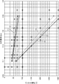
- FIG. 8 and 9 are graphs showing the relationship between the atomic ratio m (horizontal axis) of Al in the hard coating 20 and the bias voltage V (vertical axis) applied to the substrate 11.
- (2) ′ is a straight line of ⁇ 1556 m + 1022.6.
- the charged particles which are evaporated from the target 22 ⁇ / b> A and enter the base material 11 can be accelerated by the potential gradient formed in the vicinity of the base material 11, and energy can be applied.
- the magnetic field generating member 42 generates a magnetic field M extending from the target 22A toward the substrate 11 in a direction perpendicular to the discharge surface 22B.
- the hard coating 20 is formed.
- the discharge is stably maintained, and the generated plasma (ions, electrons) is less fluctuated and uniformized.
- the plasma generated by the magnetic field M lines of magnetic force
- the hard coating 20 can be formed stably and uniformly, and the hard coating 20 having a miniaturized cubic structure can be formed.
- the magnetic field M perpendicular to the discharge surface 22B of the target 22A is further increased. It can be easily generated.
- FIG. 10 shows a state in which a steel plate 60 that is a member to be pressed is installed in the mold 50.
- the mold 50 is a mold used for hot forming of the steel plate 60, for example, and is an upper mold 51 (first mold) and a lower mold 52 (second mold) that are spaced apart from each other in the vertical direction. Type).
- the upper die 51 has a convex portion 53
- the lower die 52 is formed with a concave portion 54 having a shape along the convex portion 53.
- the upper mold 51 and the lower mold 52 are configured to be movable in a direction approaching or separating from each other by a driving force from a driving source (not shown).
- a driving force from a driving source not shown.
- FIG. 10 by lowering the upper mold 51 in a state where the heated steel sheet 60 is placed on the molding surface of the lower mold 52, the steel sheet 60 is pressed by the convex portion 53. It can be formed into a shape along the recess 54 of the lower mold 52.
- a cold forming process may be performed.
- Each of the upper mold 51 and the lower mold 52 has base materials 55 and 58 constituting a main body portion of the mold, and hard films 56 and 57 coated on the surfaces of the base materials 55 and 58 by PVD. is doing. Similar to the first embodiment, the hard films 56 and 57 have a composition formula of Al m Cr 1-m N 1-xyZ C x B y O z (0.68 ⁇ m ⁇ 0.85). And having a cubic rock salt type crystal structure, H / E is 0.050 or more and 0.120 or less, and the hardness H is adjusted to 20 GPa or more and has excellent wear resistance. For this reason, not only the cutting tool illustrated in the first embodiment but also a plastic working jig such as the mold 50 can exhibit an excellent wear resistance effect.
- the mold 50 is not limited to the bending mold shown in FIG. 10, and may be another press mold such as a punching die, a drawing die, or a compression die.
- the hard film-coated member of the present invention can be applied to various machine parts that require wear resistance in addition to cutting tools and dies.
- it can be applied to sliding parts such as piston rings and valves.
- the base material 11 and the hard coating 20 are in direct contact with each other as shown in FIG. 3, and the base layer for improving the adhesion is between the base material 11 and the hard coating 20. It may be formed.
- the underlayer include those made of materials such as TiAlN, CrN, or TiN.
- the atomic ratio x of C may be outside the range of 0.05 ⁇ x ⁇ 0.5.
- the atomic ratio y of B may be less than 0.01.
- the atomic ratio z of O may be outside the range of z ⁇ 0.10.
- the hard coating 20 is formed by arc ion plating.
- the present invention is not limited to this, and the film may be formed by other physical vapor deposition methods such as sputtering.
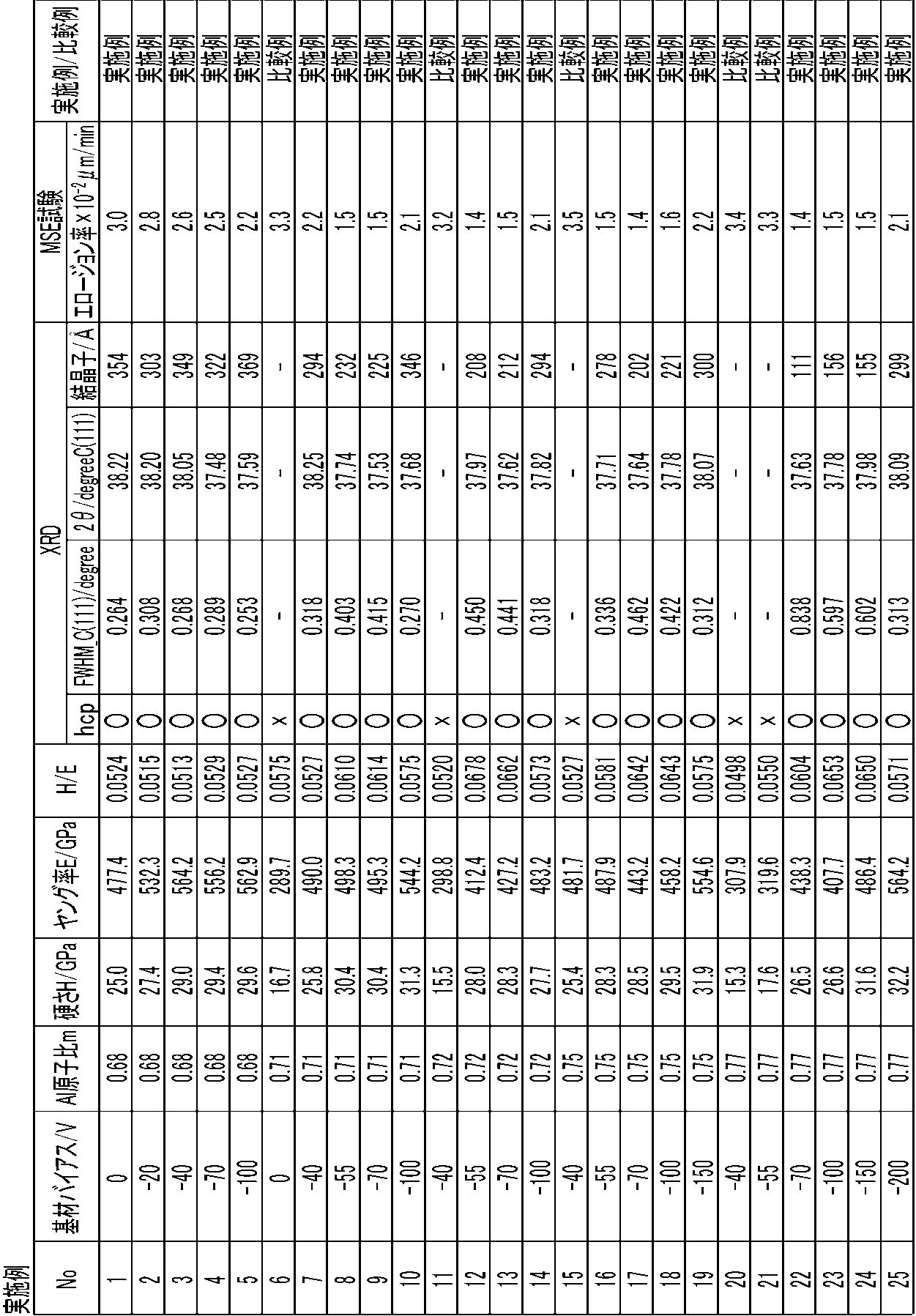
- Example 1 [Hard film formation] First, various targets 22A having different Al contents (atomic ratio) were prepared, and the hard coating 20 was formed by changing the bias voltage (base bias) V applied to the base 11. The conditions of the Al atomic ratio m and the substrate bias V of the target 22A are as shown in Table 1 (Nos. 1 to 25) below. The film formation apparatus 2 described with reference to FIGS. 5 to 7 was used for film formation.
- a mirror-finished carbide test piece (13 mm ⁇ 13 mm ⁇ 5 mm thick) was prepared as the base material 11.
- the substrate 11 was ultrasonically cleaned in ethanol, introduced into the chamber 21, and set on the stage 24.
- a target 22A made of AlCr having the component composition shown in Table 1 was prepared and connected to the negative side of the arc power source 22.
- a target having a target diameter of 100 mm ⁇ was used as the target 22A.
- the inside of the chamber 21 was evacuated to 5 ⁇ 10 ⁇ 3 Pa, the substrate 11 was heated to 500 ° C. by the heater 26, and then etching with Ar ions was performed for 5 minutes. Thereafter, nitrogen gas was introduced until the inside of the chamber 21 reached 4 Pa. Then, the hard coating 20 was formed on the surface of the substrate 11 by evaporating the target 22A with a discharge current of 150A and rotating the stage 24 at a rotation speed of 5 rpm. At this time, the bias voltage V applied to the substrate 11 by the bias power source 25 was controlled as shown in Table 1 below. A DC power source was used as the bias power source 25. The film thickness of the hard coating 20 was 3 ⁇ m.
- the hardness was measured by a nanoindenter test using a cemented carbide test piece on which the hard coating 20 was formed.
- ENT-1100 manufactured by Elionix Co., Ltd. was used as the apparatus, and a Belkovic type triangular pyramid indenter was used as the indenter.
- Five load load curves were measured under five load conditions of 2 mN, 5 mN, 7 mN, 10 mN, and 20 mN, respectively.
- the data was corrected by the method (J. Mater. Res. Vol. 16, No. 11, 2001, 3084) proposed by SAWA et al.
- SAWA et al was calculated from the hardness and Young's modulus thus determined.
- the crystallinity of the hard coating 20 formed on the base material 11 is determined by X-ray diffraction (CuK ⁇ ray, 40 kV-40 mA, ⁇ -2 ⁇ , divergence slit 1 °, divergence length limiting slit 10 mm, scattering slit 1 °. , Light receiving slit 0.15 mm, monochrome light receiving slit 0.8 mm).
- a peak based on the cubic (111) plane in the hard coating 20 was observed at a diffraction angle (2 ⁇ ) of around 38 ° (36 to 39 °) in the X-ray diffraction pattern. The presence of this peak confirmed the formation of cubic crystals.
- FWHM Full Width Half Maximum
- the wear resistance of the hard coating 20 was confirmed by an MSE (Micro Slurry-Jet Erosion) test. About each sample which formed the hard film
- the MSE test uses a slurry (3 mass%) containing amorphous alumina particles of # 8000 (average particle size 1.2 ⁇ m), a projection distance of 10 mm, a projection angle of 90 °, and a projection pressure of 0.390 MPa ( ⁇ 0.002). Within the conditions).
- the slurry was projected for a certain period of time, and the erosion depth was determined by measuring the projection mark using a stylus roughness meter, and the erosion rate ( ⁇ m / min) was calculated. An erosion rate of 3.0 ⁇ 10 ⁇ 2 ⁇ m / min or less was accepted.
- the erosion rate increased with a decrease in the bias voltage (absolute value), and the wear resistance decreased. This is presumably because the energy given to the coating surface was reduced and hexagonal crystals were formed.
- the bias voltage exceeds the upper limit ( ⁇ 1429 m + 940.3), hexagonal crystals are formed even if the Al content is within the range of 0.70 ⁇ m ⁇ 0.85, and the wear resistance is poor. .
- the bias voltage was lower than the lower limit ( ⁇ 316 V), the effect of sputtering was increased, so that an evaluable film could not be formed.
- the graph of FIG. It corresponds to Examples 1 to 25, and “x” corresponds to a comparative example.
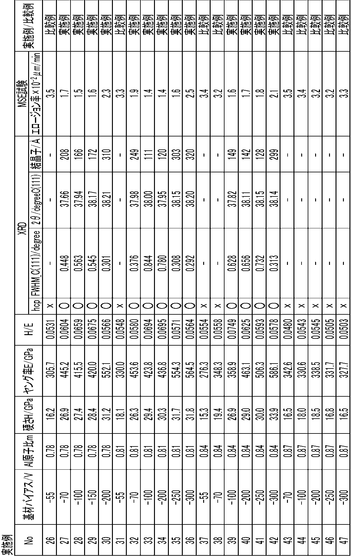
- Example 2 The conditions of the Al atomic ratio m and the substrate bias V of the target 22A were adjusted as shown in the following Table 2 and Table 3 (Nos. 1 to 47), and the same test as in Example 1 was performed.
- the bias voltage exceeds the upper limit ( ⁇ 214.3 m + 110), hexagonal crystals are formed even if the Al content is within the range of 0.7 ⁇ m ⁇ 0.85, and the wear resistance is poor. .
- the bias voltage is lower than the lower limit ( ⁇ 1666 m + 1100), the wear resistance is further improved when the bias voltage is higher than the lower limit.
- the graph of FIG. It corresponds to Examples 1 to 47, and “x” corresponds to a comparative example.
- the H / E is It turned out that the hard film 20 excellent in abrasion resistance adjusted to 0.058 or more and 0.120 or less can be formed.
- Example 1 is the same as Example 1 except that a hard film 20 containing the elements C, B, and O is formed.
- C and O were added into the film by introducing methane (CH 4 ) gas and oxygen (O) gas into the nitrogen gas during film formation.
- Boron (B) was added by putting it in the target 22A.
- the Al content was 71 at%, and the bias voltage applied to the substrate 11 was ⁇ 200V.
- Each evaluation method of the hard coating 20 was the same as that in Example 1. The test results are shown in Table 4 below. In Table 4, No. The result of 1 is indicated by a circle in the graph of FIG.
- Example 1 is the same as Example 1 except that a hard film 20 containing the elements C, B, and O is formed.
- C and O were added into the film by introducing methane (CH 4 ) gas and oxygen (O) gas into the nitrogen gas during film formation.
- Boron (B) was added by putting it in the target 41.
- the Al content was 77 at%, and the bias voltage applied to the substrate 11 was ⁇ 100V.
- Each evaluation method of the hard coating 20 was the same as that in Example 1. The test results are shown in Table 5 below.
Landscapes
- Chemical & Material Sciences (AREA)
- Engineering & Computer Science (AREA)
- Mechanical Engineering (AREA)
- Chemical Kinetics & Catalysis (AREA)
- Materials Engineering (AREA)
- Metallurgy (AREA)
- Organic Chemistry (AREA)
- Physical Vapour Deposition (AREA)
- Cutting Tools, Boring Holders, And Turrets (AREA)
Abstract
硬質皮膜20は、Al、Cr及びNの各元素を含有する皮膜である。硬質皮膜20は、立方晶岩塩型の結晶構造を有し、AlmCr1-mN1-x-y-zCxByOz(0.68≦m≦0.85、y≦0.10)の組成式からなるものである。硬質皮膜20の硬さをH(GPa)、硬質皮膜20のヤング率をE(GPa)としたときに、ヤング率に対する硬さの比であるH/Eが0.050以上0.120以下であり且つHが20GPa以上となっている。
Description
本発明は、硬質皮膜、当該硬質皮膜を備えた硬質皮膜被覆部材及び硬質皮膜の製造方法に関する。
従来、切削工具や金型など、硬質物との摺動に起因する大幅な温度上昇や摩耗が発生する工具においては、耐摩耗性を向上させるために基材の表面にセラミックス材料からなる硬質皮膜を形成する対策がなされている。例えば、下記特許文献1,2及び非特許文献1には、切削工具などの基材の表面においてAlCrNからなる硬質皮膜を形成することが開示されている。下記特許文献1及び非特許文献1には、70at%以上のAlを含有するAlCrN皮膜を基材上に形成したものが開示されている。また下記特許文献2には、70at%未満のAlを含有するAlCrN皮膜を基材上に形成したものが開示されている。
AlCrN皮膜は、CrNの結晶格子にAlが固溶した準安定状態の立方晶の結晶構造を有する。ここで、下記特許文献1及び非特許文献1のようにAl含有量が高い場合には、CrNの結晶格子にAlが固溶した状態が不安定となり、安定相である六方晶AlNが生成する。このような六方晶構造は機械的特性に劣るため、下記特許文献1及び非特許文献1では耐摩耗性に優れた硬質皮膜を得ることができない。
一方、下記特許文献2のようにAl含有量が低い皮膜は、AlCrNの粗大な立方晶が生成した結晶構造を有する。この場合、皮膜が硬くなる一方でヤング率も高くなる。このため、外部からの力に対する変形能が乏しくなるため割れに発展し易く、耐摩耗性に劣るという問題がある。
Surface & Coatings Technology、200、(2005)、2114-2122
本発明の目的は、耐摩耗性がより改善された硬質皮膜、当該硬質皮膜を備えた硬質皮膜被覆部材及び当該硬質皮膜を製造する方法を提供することである。
本発明の一局面に係る硬質皮膜は、Al、Cr及びNを含有する硬質皮膜であって、AlmCr1-mN1-x-y-zCxByOzの組成式からなるものである。前記組成式において、mは、Al、Crの合計に対するAlの原子比を示している。1-mは、Al、Crの合計に対するCrの原子比を示している。1-x-y-zは、N、C、B、Oの合計に対するNの原子比を示している。xは、N、C、B、Oの合計に対するCの原子比を示している。yは、N、C、B、Oの合計に対するBの原子比を示している。zは、N、C、B、Oの合計に対するOの原子比を示している。0.68≦m≦0.85、y≦0.10の関係式が満たされている。前記硬質皮膜は、立方晶岩塩型の結晶構造を有している。前記硬質皮膜の硬さをH(GPa)、前記硬質皮膜のヤング率をE(GPa)としたときに、ヤング率に対する硬さの比であるH/Eが0.050以上0.120以下であり且つHが20GPa以上となっている。
本発明の他の局面に係る硬質皮膜被覆部材は、基材と、前記基材の表面に形成された上記硬質皮膜と、を備えている。
本発明のさらに他の局面に係る硬質皮膜の製造方法は、AlmCr1-mN1-x-y-zCxByOzの組成式からなり、立方晶岩塩型の結晶構造を有する硬質皮膜を基材の表面に形成する方法である。前記組成式において、mは、Al、Crの合計に対するAlの原子比を示している。1-mは、Al、Crの合計に対するCrの原子比を示している。1-x-y-zは、N、C、B、Oの合計に対するNの原子比を示している。xは、N、C、B、Oの合計に対するCの原子比を示している。yは、N、C、B、Oの合計に対するBの原子比を示している。zは、N、C、B、Oの合計に対するOの原子比を示している。0.70<m≦0.85、y≦0.10の関係式が満たされる。この方法は、前記基材をステージ上に設置する工程と、前記硬質皮膜の成分組成を有するターゲットを設置する工程と、前記ターゲットを蒸発させることにより、前記基材の表面に前記硬質皮膜を成膜する工程と、を備えている。前記硬質皮膜を成膜する工程では、前記ステージから前記基材に印加するバイアス電圧Vが、-316≦V≦-214.3m+110の関係式を満たすように、前記基材にバイアス電圧を印加しつつ前記硬質皮膜を成膜する。
(本発明の実施形態の概要)
まず、本発明の実施形態に係る硬質皮膜、硬質皮膜被覆部材及び硬質皮膜の製造方法の概要について説明する。
まず、本発明の実施形態に係る硬質皮膜、硬質皮膜被覆部材及び硬質皮膜の製造方法の概要について説明する。
本発明の実施形態に係る硬質皮膜は、Al、Cr及びNを含有する硬質皮膜であって、AlmCr1-mN1-x-y-zCxByOzの組成式からなるものである。この組成において、0.68≦m≦0.85、y≦0.10の関係式が満たされている。この硬質皮膜は、立方晶岩塩型の結晶構造を有している。この硬質皮膜の硬さをH(GPa)、この硬質皮膜のヤング率をE(GPa)としたときに、ヤング率に対する硬さの比であるH/Eが0.050以上0.120以下であり且つHが20GPa以上となっている。
上記硬質皮膜では、Al含有量を0.68≦m≦0.85の範囲に調整すると共に、硬さH及びヤング率Eを調整することにより、H/Eが0.050以上0.120以下であり且つHが20GPa以上(H≧20GPa)の範囲となっている。H/Eが0.050未満の皮膜では、硬さHに対してヤング率Eが高くなり過ぎるため、外力が加わった時の皮膜の変形量が少なくなる。よって、割れが発生し易くなるため、耐摩耗性が低下する。一方で、H/Eが大き過ぎる皮膜(0.120を超える)では、ヤング率Eが低くなり過ぎるため、硬質皮膜としての機能を果たすことが困難になる。
これに対して、上記硬質皮膜は、立方晶岩塩型の結晶構造を有すると共に、硬さHが20GPa以上の範囲においてH/Eを0.050以上0.120以下の範囲に調整することにより、耐摩耗性が飛躍的に向上している。H/Eは、0.0505以上であることが好ましく、0.0510以上であることがより好ましく、0.0515以上であることがさらに好ましく、0.0520以上であることが一層好ましい。さらに、H/Eは、0.058以上であることが好ましく、0.060以上であることがより好ましく、0.061以上であることがさらに好ましい。また上限に関し、H/Eは、0.10以下であることが好ましく、0.09以下であることがより好ましい。また硬さHは、22GPa以上であることが好ましく、24GPa以上であることがより好ましく、25GPa以上であることがさらに好ましく、26GPa以上であることが一層好ましい。
上記硬質皮膜の「硬さH(GPa)」及び「ヤング率E(GPa)」は、硬質皮膜が形成された超硬試験片を用いてナノインデンテーション試験を行うことにより測定される。ナノインデンターによる測定には、装置として「株式会社エリオニクス製ENT-1100」が用いられる。またインデンターには、ベルコビッチ型の三角錐圧子が使用される。
まず、荷重2、5、7、10及び20mNの5荷重により各々5点の荷重負荷曲線を測定する。そして、SAWAらにより提案された装置のコンプライアンスと圧子先端形状を補正する方法(J.Mater.Res.Vol.16,No.11,2001,3084)によりデータの補正を行い、「硬さH(GPa)」及び「ヤング率E(GPa)」を算出する。その測定値からH/E(-)の値を算出することができる。
また上記硬質皮膜におけるAl、Cr、N、C、B、Oの各原子比は、エネルギー分散型X線分析装置(Energy Dispersive X-ray Spectrometer)を用いて測定することができる。
上記硬質皮膜では、CuKα線を用いたX線回折測定において、前記立方晶岩塩型の結晶構造の(111)面に基づくピークの半値幅は、0.25°以上1.00°以下であることが好ましい。
上記硬質皮膜では、結晶中における極微細な六方晶の生成及び成膜時のイオン衝突による歪に起因して立方晶の成長が阻害され、その結果立方晶の結晶粒が小さくなっている。このため、X線回折測定を行った場合に、立方晶岩塩型の結晶構造の(111)面に基づくピークの半値幅が0.25°以上1.00°以下となる。半値幅がこの範囲内になるように立方晶が微細化された皮膜では、H/Eの範囲が上記の通り0.050以上0.120以下の範囲に調整される。なお、結晶中の極微細な六方晶は、X線回折測定では検出できない程度の大きさのものである。
半値幅が0.25°未満である場合には、立方晶の結晶粒が大きく成長しており、H/Eが0.050以上0.120以下の範囲よりも小さくなる。一方で、半値幅が1.00°を超える場合には、立方晶の結晶粒が微細化し過ぎるため、結晶粒ごと脱落し易くなり、耐摩耗性が低下する。このため、半値幅の範囲は、0.25°以上1.00°以下であることが好ましい。また半値幅の下限は、0.255°以上であることが好ましく、0.26°以上であることがより好ましく、0.265°以上であることがさらに好ましい。さらに、半値幅の下限は、0.32°以上であることが好ましく、0.35°以上であることがより好ましく、0.37°以上であることがさらに好ましく、0.40°以上であることが一層好ましい。また半値幅の上限は、0.95°以下であることがより好ましく、0.90°以下であることがさらに好ましく、0.85°以下であることが一層好ましい。
また上記のように、極微細な六方晶と微細化された立方晶とが混在した硬質皮膜を得るためには、皮膜中のAl含有量の調整も必要である。Al含有量が低すぎる場合には、極微細な六方晶が生成しない。このため、上記硬質皮膜では、Alの原子比mが0.68以上であり、0.70を超えることが好ましく、0.71を超えることがより好ましく、0.72以上であることがさらに好ましく、0.75以上であることが一層好ましい。一方で、Al含有量が高すぎる場合には、立方晶が生成しない。このため、上記硬質皮膜では、Alの原子比mが0.85以下であり、0.82以下であることが好ましく、0.80以下であることがより好ましく、0.78以下であることがさらに好ましい。
上記硬質皮膜では、Cの原子比xが0.05≦x<0.5の関係式を満たしていてもよい。またBの原子比yがy≦0.10の関係式を満たし、さらに0.01≦yの関係式を満たしていてもよい。またOの原子比zが0<z<0.10の関係式を満たしていてもよい。
上記硬質皮膜は、窒化物をベースとするものであるが、さらなる機能を付与するために、炭素(C),ホウ素(B),酸素(O)などの元素をさらに含有していてもよい。Cは、結晶中において炭化物を形成することにより、皮膜の硬さを向上させる。このような効果を得るため、Cの原子比xは0.05以上であることが好ましい。しかし、C含有量が過剰になると、皮膜の耐熱性が低下するため、Cの原子比xは0.5未満であることが好ましい。
Bは、皮膜中のNと結合することにより固体潤滑剤であるホウ化窒素を形成し、皮膜に潤滑作用を付与する。このような効果を得るため、Bの原子比yは0.01以上であることが好ましい。しかし、B含有量が過剰になると皮膜の硬さが低下するため、Bの原子比yは0.10以下であり、0.08以下であることがより好ましい。またOは、Al2O3の形成により皮膜の硬さを向上させる目的で添加することができるが、O含有量が過剰になると耐摩耗性が低下する。このため、Oの原子比zは、0.1未満であることが好ましい。
本実施形態に係る硬質皮膜被覆部材は、基材と、前記基材の表面に形成された上記硬質皮膜と、を備えている。上記硬質皮膜被覆部材は、耐摩耗性に優れた上記硬質皮膜が基材の表面に形成されたものである。このため、上記硬質皮膜被覆部材は、切削工具や金型など、硬質物との激しい摺動環境下で使用され、高い耐摩耗性が要求される工具において好適に用いることができる。
本実施形態に係る硬質皮膜の製造方法は、AlmCr1-mN1-x-y-zCxByOzの組成式からなり、立方晶岩塩型の結晶構造を有する硬質皮膜を基材の表面に形成する方法である。この組成において、0.70<m≦0.85、y≦0.10の関係式が満たされる。この方法は、前記基材をステージ上に設置する工程と、前記硬質皮膜の成分組成を有するターゲットを設置する工程と、前記ターゲットを蒸発させることにより、前記基材の表面に前記硬質皮膜を成膜する工程と、を備えている。前記硬質皮膜を成膜する工程では、前記ステージから前記基材に印加するバイアス電圧Vが、-316≦V≦-214.3m+110の関係式を満たすように、前記基材にバイアス電圧を印加しつつ前記硬質皮膜を成膜する。バイアス電圧Vの下限は、-1666m+1100であることが好ましい。
上記硬質皮膜の製造方法では、基材に対して上記範囲内に制御されたバイアス電圧Vを印加しつつ硬質皮膜を成膜する。Al含有量が多い(0.70<m)硬質皮膜では、安定相である六方晶が生成し易い。これに対して、上記製造方法では、適切な範囲内に制御されたバイアス電圧Vを基材に印加することにより、ターゲットから蒸発して基材に入射する荷電粒子にエネルギーを付与することができる。このため、高エネルギーの荷電粒子により成膜中の皮膜表面へのスパッタリングを行うことができる。これにより、成膜中の皮膜表面のエネルギーを高め、且つ局部的に不安定な状態にすることができる。よって、準安定相である立方晶が生成すると共に、極微細な六方晶によって当該立方晶の結晶粒が微細化された皮膜を成膜することができる。その結果、H/Eが0.050以上0.120以下で且つ硬さHが20GPa以上の範囲に調整された耐摩耗性に優れる上記硬質皮膜を得ることができる。
バイアス電圧Vが上記範囲よりも高い場合には、皮膜中に粗大な六方晶が形成されるため、H/Eが大きくなる一方で皮膜の硬さHが低くなる。一方で、バイアス電圧Vが上記範囲よりも低い場合には、基材に入射する荷電粒子のエネルギーが高くなり過ぎるため、皮膜の形成速度よりもスパッタリング速度の影響の方が大きくなる。このため、硬質皮膜の形成が困難になる。これに対して、上記の通りバイアス電圧Vを適切に制御することにより、H/Eが0.050以上0.120以下で且つ硬さHが20GPa以上の範囲に調整された耐摩耗性に優れる硬質皮膜を成膜することができる。
上記硬質皮膜の製造方法では、前記硬質皮膜を成膜する工程において、前記ターゲットの放電面に対して垂直な方向に磁場を発生させる。
上記のように、H/E及び硬さHが適切な範囲に調整された耐摩耗性に優れる硬質皮膜を得るためには、皮膜の安定且つ均一な形成が重要となる。これに対して、プラズマを形成する蒸発源において、ターゲット放電面に対して垂直な磁場を構成することにより、放電が安定して持続するようになり、発生するプラズマ(イオン、電子)の揺らぎが少なく均一になる。さらに、磁力線が放電面に対して垂直に伸びることにより、発生したプラズマがターゲットに到達し易くなり、安定した膜成長が可能になる。
(本発明の実施形態の詳細)
以下、図面に基づいて、本発明の実施形態に係る硬質皮膜、硬質皮膜被覆部材及び硬質皮膜の製造方法について詳細に説明する。
以下、図面に基づいて、本発明の実施形態に係る硬質皮膜、硬質皮膜被覆部材及び硬質皮膜の製造方法について詳細に説明する。
<実施形態1>
[硬質皮膜被覆部材]
まず、本発明の実施形態1に係る硬質皮膜被覆部材であるインサート10について、図1及び図2を参照して説明する。図1は、インサート10の全体構造を模式的に示す斜視図である。図2は、インサート10により被削材100を切削加工する様子を模式的に示す図である。なお、本発明の硬質皮膜被覆部材は、以下に説明するインサート10などの旋削加工用切削工具以外にも、例えばドリルビットなどの穴あけ加工用切削工具、タップなどのネジ切り加工用切削工具、エンドミルなどの転削加工用切削工具又はブレードなどの切断加工用切削工具などの種々の切削工具に適用することができる。
[硬質皮膜被覆部材]
まず、本発明の実施形態1に係る硬質皮膜被覆部材であるインサート10について、図1及び図2を参照して説明する。図1は、インサート10の全体構造を模式的に示す斜視図である。図2は、インサート10により被削材100を切削加工する様子を模式的に示す図である。なお、本発明の硬質皮膜被覆部材は、以下に説明するインサート10などの旋削加工用切削工具以外にも、例えばドリルビットなどの穴あけ加工用切削工具、タップなどのネジ切り加工用切削工具、エンドミルなどの転削加工用切削工具又はブレードなどの切断加工用切削工具などの種々の切削工具に適用することができる。
インサート10は、被削材100の切削加工に用いられる工具であり、不図示のシャンクの先端に取り付けて使用される。インサート10は、工具の母材である基材11と、基材11の表面にコーティングされた硬質皮膜20と、を有している。
基材11は、例えば超硬合金、ダイヤモンド、金属炭化物を含む鉄基合金、サーメット又は高速度工具鋼などの硬質な材料からなる。基材11は、被削材100に食い込んですくい上げる部分であるすくい面31と、被削材100との接触を避けるために逃がされた部分である逃げ面32と、を有している。すくい面31と逃げ面32とが繋がる部分において、切れ刃33が形成されている。
図2に示すように、切れ刃33を被削材100の表面に食い込ませるようにインサート10を移動させることにより当該被削材100の表面が切削され、これにより生じた切り屑101はすくい面31上を通過する。このような切削加工においては、インサート10と被削材100との間の激しい摺動により硬質皮膜20の摩耗が進行する。これに対して、本実施形態に係るインサート10では、耐摩耗性に優れた硬質皮膜20が基材11の表面にコーティングされることにより、工具寿命が長くなっている。以下、本実施形態に係る硬質皮膜20について詳細に説明する。
[硬質皮膜]
次に、本実施形態に係る硬質皮膜20について、図3を参照して説明する。図3は、インサート10における基材11及び硬質皮膜20を含む厚さ方向の断面構造を部分的に示している。硬質皮膜20は、例えばアークイオンプレーティング(AIP)やスパッタリングなどの物理蒸着法(PVD)により、基材11の表面に耐摩耗層として形成されている。硬質皮膜20は、少なくともAl、Cr及びNの元素を含有し、その組成式がAlmCr1-mN1-x-y-zCxByOzのように表される。この組成式において、「m」は、Al,Crの合計に対するAlの原子比を示している。「1-m」は、Al,Crの合計に対するCrの原子比を示している。「1-x-y-z」は、N,C,B,Oの合計に対するNの原子比を示している。「x」は、N,C,B,Oの合計に対するCの原子比を示している。「y」は、N,C,B,Oの合計に対するBの原子比を示している。「z」は、N,C,B,Oの合計に対するOの原子比を示している。
次に、本実施形態に係る硬質皮膜20について、図3を参照して説明する。図3は、インサート10における基材11及び硬質皮膜20を含む厚さ方向の断面構造を部分的に示している。硬質皮膜20は、例えばアークイオンプレーティング(AIP)やスパッタリングなどの物理蒸着法(PVD)により、基材11の表面に耐摩耗層として形成されている。硬質皮膜20は、少なくともAl、Cr及びNの元素を含有し、その組成式がAlmCr1-mN1-x-y-zCxByOzのように表される。この組成式において、「m」は、Al,Crの合計に対するAlの原子比を示している。「1-m」は、Al,Crの合計に対するCrの原子比を示している。「1-x-y-z」は、N,C,B,Oの合計に対するNの原子比を示している。「x」は、N,C,B,Oの合計に対するCの原子比を示している。「y」は、N,C,B,Oの合計に対するBの原子比を示している。「z」は、N,C,B,Oの合計に対するOの原子比を示している。
硬質皮膜20は、極微細な六方晶が生成すると共に立方晶が生成し、この極微細な六方晶により立方晶の結晶成長が阻害されることにより、立方晶の結晶粒が微細化されたものとなっている。即ち、硬質皮膜20は、微細化された立方晶と極微細な六方晶とが混在したものとなっている。このような特徴的な結晶構造を有することから、硬質皮膜20の硬さをH(GPa)、硬質皮膜20のヤング率をE(GPa)としたときに、ヤング率Eに対する硬さHの比であるH/Eが0.050以上0.120以下であり且つ硬さHが20GPa以上となっている。
H/Eが0.050未満の場合には、皮膜の硬さに対してヤング率が高くなり過ぎるため、皮膜に外力が加わった時の変形量が少なくなる。よって、皮膜の割れが発生し易くなるため、耐摩耗性が低下する。これに対して、硬質皮膜20では、硬さHが20GPa以上の範囲においてH/Eを0.050以上に調整することにより、耐摩耗性が飛躍的に向上している。一方、H/Eが過大になると(0.120を超えると)、ヤング率が低くなり過ぎるため、硬質皮膜として機能させることが困難になる。このため、硬質皮膜20では、H/Eが0.120以下に調整されている。H/Eは、好ましくは0.058以上である。
このように、極微細な六方晶によって立方晶が微細化された結晶構造は、X線回折測定により確認することができる。硬質皮膜20は、立方晶岩塩型の結晶構造を有している。硬質皮膜20は、CuKα線を用いたX線回折測定を行った場合、立方晶岩塩型の結晶構造の(111)面に基づく回折角度38°付近のピークの半値幅が、0.25°以上1.00°以下となる。なお、極微細な六方晶は、X線回折測定では検出できない程度の大きさである。
X線回折測定において半値幅が0.25°未満である場合、立方晶の結晶粒が大きく成長しており、H/Eが小さくなる。一方で、半値幅が1.00°を超える場合には、立方晶が微細化し過ぎるため、結晶粒ごと脱落し易くなり、耐摩耗性が低下する。よって、X線回折測定による半値幅が0.25°以上1.00°以下であることを確認することにより、皮膜中において立方晶が適度に微細化された結晶構造を確認することができる。半値幅は、好ましくは0.32°以上である。
また、X線回折測定における立方晶の(111)面に基づくピークの位置及び半値幅により、t=λ/Bcosθ(シュラーの式)、を用いて、結晶子サイズt(Å)を算出することができる。λは、X線の波長(Å)である。Bは、半値幅(ラジアン)である。θは、ピーク位置2θ(ラジアン)の半分である。結晶子サイズは、400Å以下となっており、好ましくは375Å以下となっており、より好ましくは360Å以下となっている。さらに好ましくは、結晶子サイズは、290Å以下であってもよいし、285Å以下であってもよいし、280Å以下であってもよい。しかし、結晶子が微細化し過ぎると、皮膜の硬さが低下する。このため、結晶子サイズは40Å以上であり、好ましくは50Å以上であり、より好ましくは70Å以上である。
また、このように極微細な六方晶と微細化された立方晶とが混在した皮膜を得るためには、皮膜中のAl含有量を調整する必要がある。このため、Al含有量は、0.68≦m≦0.85の範囲に調整されている。Al含有量が0.68未満である場合には極微細な六方晶が生成しない。一方で、Al含有量が0.85を超える場合には、立方晶が生成せず、皮膜全体が粗大な六方晶になる。このため、Al含有量は、0.68≦m≦0.85の範囲に調整されている。Al含有量は、好ましくは0.70<mである。
また硬質皮膜20は、Al、Cr及びNのみを元素として含有するものでもよいが、さらにC、B、Oなどの元素が添加されていてもよい。これにより、硬質皮膜20に様々な機能を付与することができる。Cは、結晶中においてAlCやCrCなどの炭化物を形成することにより、皮膜の硬さを向上させる。この効果を得るため、硬質皮膜20では、Cの原子比xが0.05以上に調整されている。しかし、C含有量が過剰になると、皮膜の耐熱性が低下する。これを防止するため、硬質皮膜20では、Cの原子比xが0.5未満に調整されている。
Bは、皮膜中のNと結合することにより固体潤滑剤であるホウ化窒素を形成し、硬質皮膜20に潤滑作用を付与する。この効果を得るため、硬質皮膜20では、Bの原子比yが0.01以上に調整されている。しかし、B含有量が過剰になると硬さが低下する。これを防止するため、硬質皮膜20では、Bの原子比yが0.10以下に調整されている。
Oは、皮膜中のAlと結合して硬質なAl2O3を形成することにより、硬質皮膜20の硬さを向上させる。しかし、皮膜中のO含有量が過剰になると、皮膜の耐摩耗性が低下する。このため、硬質皮膜20では、Oの原子比zが0.1未満に調整されている。
なお、C,B,Oは、いずれも硬質皮膜20において必須の添加元素ではない。硬質皮膜20は、Al、Cr及びNのみを含有する皮膜であってもよい(x,y,z=0)。硬質皮膜20は、Al、Cr、N及びCを含有する皮膜であってもよい(y,z=0)。硬質皮膜20は、Al、Cr、N及びBを含有する皮膜であってもよい(x,z=0)。硬質皮膜20は、Al、Cr、N及びOを含有する皮膜であってもよい(x,y=0)。硬質皮膜20は、Al、Cr、N、C及びBを含有する皮膜であってもよい(z=0)。硬質皮膜20は、Al、Cr、N、C及びOを含有する皮膜であってもよい(y=0)。硬質皮膜20は、Al、Cr、N、B及びOを含有する皮膜であってもよい(x=0)。硬質皮膜20は、Al、Cr、N、C、B及びOを含有する皮膜であってもよい。
[硬質皮膜の製造方法]
次に、上記硬質皮膜20の製造方法について、図4のフローチャートに沿って説明する。図5は、硬質皮膜20の成膜に使用される成膜装置2を平面視した模式図である。まず、成膜装置2の構成について、図5を主に参照して説明する。
次に、上記硬質皮膜20の製造方法について、図4のフローチャートに沿って説明する。図5は、硬質皮膜20の成膜に使用される成膜装置2を平面視した模式図である。まず、成膜装置2の構成について、図5を主に参照して説明する。
成膜装置2は、チャンバー21と、複数(2つ)のアーク電源22及びスパッタ電源23と、ステージ24と、バイアス電源25と、複数(4つ)のヒータ26と、放電用直流電源27と、フィラメント加熱用交流電源28と、を有する。チャンバー21には、真空排気するためのガス排気口21Aと、チャンバー21内にガスを供給するためのガス供給口21Bと、が設けられている。アーク電源22の負バイアス側がアーク蒸発源(ターゲット)22Aに接続され、スパッタ電源23の負バイアス側がスパッタ蒸発源(ターゲット)23Aに接続される。またアーク電源22及びスパッタ電源23の正バイアス側がチャンバー21に接続されている。ステージ24は、回転可能に構成され、成膜対象である基材11を支持するための支持面を有する。バイアス電源25は、ステージ24を通して基材11に負バイアスを印加する。
また図6に示すように、成膜装置2は、カソードであるターゲット22Aの近傍に配置された1つの磁場発生部材42を備えている。磁場発生部材42は、例えば電磁コイル又は永久磁石であり、チャンバー21の外の大気側に配置されている。これにより、ターゲット22Aの放電面22Bに対して垂直な方向に、ターゲット22Aから基材11に向かって伸びるように磁場Mを発生させることができる。また図7に示すように、カソード冷却面22Cよりも基材11側においてターゲット22Aを挟むように2つの磁場発生部材42を配置してもよい。なお、磁場発生部材42は、3つ以上配置されていてもよい。
次に、上記成膜装置2を用いて実施される硬質皮膜20の製造方法について説明する。まず、基材11をステージ24上に設置する工程S10が実施される。この工程S10では、まず、基材11をエタノールなどの洗浄液を用いて洗浄する。そして、洗浄後の基材11をチャンバー21内に導入し、ステージ24上に設置する。
次に、ターゲット22Aを設置する工程S20が実施される。この工程S20では、成膜すべき硬質皮膜20の成分組成(0.70<m≦0.85)を有するAlCrターゲットを準備し、これをカソードとして作用させるべく、アーク電源22の負バイアス側に接続する。またBを含有する硬質皮膜20を成膜する場合には、AlCrBターゲットを準備し、同様にこれを設置する。
ターゲット22Aにおいては、Crの平均粒径は、150μm未満であり、好ましくは120μm未満であり、より好ましくは100μm未満である。またAlの平均粒径は、120μm未満であり、好ましくは110μm未満であり、より好ましくは100μm未満である。Cr及びAlの平均粒径を小さくすることにより、ターゲット22Aの放電面22Bにおいて均一に放電を起こすことができる。このため、基材11に到達する荷電粒子の濃度の揺らぎが小さくなり、安定した結晶成長が可能になる。一方で、Cr及びAlの平均粒径が小さくなり過ぎると、粉末を固化する際に金属間化合物が生成し易くなる。これを防ぐため、Cr及びAlの平均粒径は、いずれも10μm以上であり、20μm以上であることが好ましく、30μm以上であることがより好ましい。
次に、基材11をエッチングする工程S30が実施される。この工程S30では、まず、ガス排気口21Aよりチャンバー21内が所定の圧力まで減圧され、真空状態とされる。次に、ガス供給口21BからArガスがチャンバー21内に導入され、ヒータ26により基材11が所定の温度に加熱される。そして、基材11の表面がArイオンにより所定時間エッチングされる。これにより、基材11の表面に形成された酸化皮膜などが除去される。なお、この工程S30は、本発明の硬質皮膜の製造方法において必須の工程ではなく、省略されてもよい。
次に、硬質皮膜20を成膜する工程S40が実施される。この工程S40では、ガス供給口21BからN2ガスを導入することにより、チャンバー21内が所定の成膜圧力に調整される。そして、所定のアーク電流を流すことによりターゲット22Aを蒸発させると共に、ステージ24を所定の回転速度で回転させる。これにより、蒸発したターゲット材料が基材11の表面に堆積し、基材11の表面に硬質皮膜20が成膜される。
なお、C,Oの元素を含有する硬質皮膜20を成膜する場合には、メタンやアセチレンなどの炭化水素ガス、酸素ガスや水蒸気などの含酸素ガスがチャンバー21内に導入され、この状態で成膜が行われる。またBを含有する硬質皮膜20を成膜する場合であって、ターゲット22AにBを含有させない場合には、フッ化ホウ素(BF3)ガスがチャンバー21内に導入されてもよい。
この工程S40では、バイアス電源25によってステージ24から基材11に所定のバイアス電圧Vが印加された状態で硬質皮膜20が成膜される。具体的には、ステージ24から基材11に印加するバイアス電圧Vが、-316≦V≦-214.3m+110の関係式を満たすように、当該バイアス電圧Vの値が調整される。バイアス電圧Vの下限は、-310であってもよいし、-300であってもよいし、-1666m+1100であってもよいし、-1556m+1022.6であってもよいし、-1429m+940.3であってもよい。またバイアス電圧の上限は、-267m+147であってもよいし、-250m+132.5であってもよい。なお、バイアス電圧Vは、直流電圧であってもよいし、交流電圧であってもよい。特にmが0.70を超えると、20GPaを超える立方晶を形成するためにバイアス電圧の制御が必要である。これは、mが0.70を超えると成膜初期に粗大な立方晶が形成され易くなるためと考えられる。このようなバイアス電圧の制御の観点から、上限式(V=-214.3m+110)が規定される。
図8及び図9は、硬質皮膜20におけるAlの原子比m(横軸)と、基材11に印加するバイアス電圧V(縦軸)との関係を示すグラフである。図8のグラフ中、(1)は、バイアス電圧Vの上限を示すV=-214.3m+110の直線である。(1)’は、V=-267m+147の直線である。(1)’’は、V=-250m+132.5の直線である。(2)は、V=-1666m+1100の直線である。(2)’は、-1556m+1022.6の直線である。(2)’’は、V=-1429m+940.3の直線である。
図9のグラフ中、(1)は、V=-1429m+940.3の直線である。(1)’は、V=-1556m+1022.6の直線である。(1)’’は、V=-1600m+1053.4の直線である。(1)’’’は、V=-1665m+1098.9の直線である。(2)は、バイアス電圧Vの下限を示すV=-316の直線である。(2)’は、V=-310の直線である。(2)’’は、V=-300Vの直線である。
本実施形態では、図8のグラフにおいて、直線(1)、直線(2)、m=0.7の直線及びm=0.85の直線により囲まれる領域内の条件によって硬質皮膜20の成膜が行われる。また、直線(1)’、直線(2)’、m=0.7の直線及びm=0.85の直線により囲まれる領域内の条件がより好ましく、直線(1)’’、直線(2)’’、m=0.7の直線及びm=0.85の直線により囲まれる領域内の条件がさらに好ましい。
また図8のグラフに示した成膜条件には限定されない。図9のグラフにおいて、直線(1)、直線(2)、m=0.7の直線及びm=0.85の直線により囲まれる領域内の条件によって硬質皮膜20の成膜が行われてもよい。また、直線(1)’、直線(2)’、m=0.7の直線及びm=0.85の直線により囲まれる領域内の条件が採用されてもよいし、直線(1)’’、直線(2)’’、m=0.7の直線及びm=0.845の直線により囲まれる領域内の条件が採用されてもよいし、直線(1)’’’、直線(2)’’、m=0.7の直線及びm=0.84の直線により囲まれる領域内の条件が採用されてもよい。これにより、ターゲット22Aから蒸発して基材11に入射する荷電粒子を、基材11の近傍に形成される電位勾配によって加速し、エネルギーを付与することができる。このような高エネルギーの荷電粒子を基材11に衝突させ、且つスパッタリングによってさらに皮膜表面のエネルギーを高めることにより、エネルギー的に安定な六方晶が生成せず、準安定相である微細な立方晶が生成する。その結果、H/Eが0.050以上0.120以下であり且つ硬さHが20GPa以上に調整された硬質皮膜20を成膜することができる。
また図6及び図7に示すように、この工程S40では、磁場発生部材42により、放電面22Bに対して垂直な方向に、ターゲット22Aから基材11に向かって伸びる磁場Mを発生させた状態で硬質皮膜20が成膜される。これにより、放電が安定して持続するようになり、発生するプラズマ(イオン、電子)の揺らぎが少なく均一化される。そして、放電面22Bに対して垂直に延びる磁場M(磁力線)によって発生したプラズマが基材11に到達し易くなり、安定した成膜が可能になる。これにより、硬質皮膜20の安定且つ均一な形成が可能となり、微細化された立方晶構造を有する硬質皮膜20を成膜することができる。特に、図7に示すように、カソード冷却面22Cよりも基材11側に磁場発生部材42(永久磁石又は電磁コイル)を配置することにより、ターゲット22Aの放電面22Bに垂直な磁場Mをより容易に発生させることができる。
<実施形態2>
次に、本発明の実施形態2に係る硬質皮膜被覆部材である金型50について、図10を参照して説明する。図10は、金型50において被プレス部材である鋼板60が設置された状態を示している。
次に、本発明の実施形態2に係る硬質皮膜被覆部材である金型50について、図10を参照して説明する。図10は、金型50において被プレス部材である鋼板60が設置された状態を示している。
金型50は、例えば鋼板60の熱間成形に用いられる金型であって、上下方向に互いに離間して配置された上金型51(第1金型)及び下金型52(第2金型)を有している。上金型51は凸部53を有し、下金型52には凸部53に沿った形状の凹部54が形成されている。上金型51及び下金型52は、不図示の駆動源からの駆動力により互いに接近する方向又は互いに離間する方向に移動可能に構成されている。図10に示すように、加熱された鋼板60が下金型52の成形面上に設置された状態で上金型51を下降させ、凸部53によって鋼板60をプレスすることにより、鋼板60を下金型52の凹部54に沿った形状に成形することができる。なお、熱間成形加工に限定されず、冷間成形加工が行われてもよい。
上金型51及び下金型52の各々は、金型の本体部分を構成する基材55,58と、PVDによって基材55,58の表面にコーティングされた硬質皮膜56,57と、を有している。この硬質皮膜56,57は、上記実施形態1と同様に、AlmCr1-mN1-x-y-zCxByOz(0.68≦m≦0.85)の組成式からなると共に立方晶岩塩型の結晶構造を有し、H/Eが0.050以上0.120以下で且つ硬さHが20GPa以上に調整された耐摩耗性に優れたものとなっている。このため、上記実施形態1において例示した切削工具だけでなく、金型50のような塑性加工用治工具においても優れた耐摩耗性の効果を発現することができる。なお、金型50は、図10に示す曲げ型に限定されず、抜き型、絞り型又は圧縮型などの他のプレス金型であってもよい。
<その他実施形態>
次に、本発明のその他実施形態について説明する。
次に、本発明のその他実施形態について説明する。
本発明の硬質皮膜被覆部材は、切削工具や金型以外にも、耐摩耗性が要求される種々の機械部品においても適用することができる。例えば、ピストンリングやバルブなどの摺動部品にも適用することができる。
上記実施形態1において、図3に示すように基材11と硬質皮膜20とが直接接触する場合に限定されず、密着性向上のための下地層が基材11と硬質皮膜20との間に形成されてもよい。下地層としては、TiAlN、CrN又はTiNなどの材料からなるものが挙げられる。
上記実施形態1,2において、Cの原子比xは0.05≦x<0.5の範囲外であってもよい。またBの原子比yは、0.01未満であってもよい。またOの原子比zは、z<0.10の範囲外であってもよい。
上記実施形態1では、アークイオンプレーティングにより硬質皮膜20を成膜する場合について説明したがこれに限定されず、例えばスパッタリングなど他の物理蒸着法によって成膜してもよい。
硬質皮膜の耐摩耗性について、本発明の効果を確認する実験を行った。
(実施例1)
[硬質皮膜の成膜]
まず、Al含有量(原子比)が異なる種々のターゲット22Aを準備し、且つ、基材11に印加されるバイアス電圧(基材バイアス)Vを変化させて硬質皮膜20の成膜を行った。ターゲット22AのAl原子比m及び基材バイアスVの条件は、下記の表1(No.1~25)に示す通りである。また成膜には、図5~図7を参照して説明した成膜装置2を使用した。
[硬質皮膜の成膜]
まず、Al含有量(原子比)が異なる種々のターゲット22Aを準備し、且つ、基材11に印加されるバイアス電圧(基材バイアス)Vを変化させて硬質皮膜20の成膜を行った。ターゲット22AのAl原子比m及び基材バイアスVの条件は、下記の表1(No.1~25)に示す通りである。また成膜には、図5~図7を参照して説明した成膜装置2を使用した。
まず、基材11として、鏡面の超硬試験片(13mm×13mm×5mm厚)を準備した。そして、基材11をエタノール中にて超音波洗浄し、チャンバー21内に導入し、ステージ24上にセットした。また表1に示す成分組成のAlCrからなるターゲット22Aを準備し、アーク電源22のマイナス側に接続した。ターゲット22Aとしては、ターゲット径100mmφのものを使用した。
次に、チャンバー21内を5×10⁻³Paまで排気し、ヒータ26により基材11を500℃まで加熱した後、Arイオンによるエッチングを5分間行った。その後、チャンバー21内が4Paになるまで窒素ガスを導入した。そして、150Aの放電電流によりターゲット22Aを蒸発させると共にステージ24を5rpmの回転速度で回転させることにより、基材11の表面に硬質皮膜20を成膜した。このとき、バイアス電源25により基材11に印加するバイアス電圧Vを、下記の表1の通り制御した。バイアス電源25としては、直流電源を用いた。硬質皮膜20の膜厚は、3μmとした。
[硬さ・ヤング率の測定]
成膜後の硬質皮膜20について、ナノインデンターを用いて硬さH(GPa)及びヤング率E(GPa)を測定し、H/Eの値を算出した。
成膜後の硬質皮膜20について、ナノインデンターを用いて硬さH(GPa)及びヤング率E(GPa)を測定し、H/Eの値を算出した。
硬さは、硬質皮膜20が形成された超硬試験片を用いて、ナノインデンター試験により測定した。ナノインデンターによる測定には、株式会社エリオニクス製ENT-1100を装置として用い、インデンターにはベルコビッチ型の三角錐圧子を使用した。まず、2mN、5mN、7mN、10mN及び20mNの5つの荷重条件によって各々5点の荷重負荷曲線を測定した。そして、SAWA等により提案された、装置のコンプライアンスと圧子先端形状を補正する方法(J.Mater.Res.Vol.16,No.11,2001,3084)によりデータの補正を行った。このようにして求められた硬さ及びヤング率からH/Eの値を算出した。
[X線回折測定]
各サンプルについて、基材11上に形成された硬質皮膜20の結晶性を、X線回折(CuKα線、40kV-40mA、θ-2θ、発散スリット1°、発散縦制限スリット10mm、散乱スリット1°、受光スリット0.15mm、モノクロ受光スリット0.8mm)により調査した。硬質皮膜20における立方晶(111)面に基づくピークは、X線回折パターンにおいて回折角度(2θ)が38°付近(36~39°)に観測された。このピークの存在により、立方晶の生成を確認した。また当該ピークの半値幅(FWHM:Full Width Half Maximum)を計算により算出した。また回折角度59°付近において六方晶由来の(110)面に基づくピークが認められた場合は、皮膜が完全に六方晶化していると判断した。下記の表1において、完全な六方晶化が認められた場合には、「hcp(hexagonal close-packed)」の欄に「×」印を付している。また、立方晶(111)面に基づくピークの位置及び半値幅(FWHM)により、シュラーの式(t=λ/Bcosθ)を用いて、結晶子サイズt(Å)を算出した。λはX線の波長(Å)、Bは半値幅(ラジアン)、θはピーク位置2θ(ラジアン)をそれぞれ示す。
各サンプルについて、基材11上に形成された硬質皮膜20の結晶性を、X線回折(CuKα線、40kV-40mA、θ-2θ、発散スリット1°、発散縦制限スリット10mm、散乱スリット1°、受光スリット0.15mm、モノクロ受光スリット0.8mm)により調査した。硬質皮膜20における立方晶(111)面に基づくピークは、X線回折パターンにおいて回折角度(2θ)が38°付近(36~39°)に観測された。このピークの存在により、立方晶の生成を確認した。また当該ピークの半値幅(FWHM:Full Width Half Maximum)を計算により算出した。また回折角度59°付近において六方晶由来の(110)面に基づくピークが認められた場合は、皮膜が完全に六方晶化していると判断した。下記の表1において、完全な六方晶化が認められた場合には、「hcp(hexagonal close-packed)」の欄に「×」印を付している。また、立方晶(111)面に基づくピークの位置及び半値幅(FWHM)により、シュラーの式(t=λ/Bcosθ)を用いて、結晶子サイズt(Å)を算出した。λはX線の波長(Å)、Bは半値幅(ラジアン)、θはピーク位置2θ(ラジアン)をそれぞれ示す。
[エロージョン率測定]
MSE(Micro Slurry-Jet Erosion)試験により、硬質皮膜20の耐摩耗性を確認した。硬質皮膜20を超硬合金製の基材11上に成膜した各サンプルについて、MSE試験によりエロージョン率を測定し、耐摩耗性を評価した。MSE試験は、#8000(平均粒径1.2μm)の不定形アルミナ粒子を含有するスラリー(3mass%)を使用し、投射距離10mm、投射角度90°、投射圧力0.390MPa(±0.002以内)の条件で行った。そして、一定時間スラリーを投射し、触針式粗さ計を用いて投射痕を測定することによりエロージョン深さを求め、エロージョン率(μm/min)を算出した。エロージョン率が3.0×10-2μm/min以下のものを合格とした。
MSE(Micro Slurry-Jet Erosion)試験により、硬質皮膜20の耐摩耗性を確認した。硬質皮膜20を超硬合金製の基材11上に成膜した各サンプルについて、MSE試験によりエロージョン率を測定し、耐摩耗性を評価した。MSE試験は、#8000(平均粒径1.2μm)の不定形アルミナ粒子を含有するスラリー(3mass%)を使用し、投射距離10mm、投射角度90°、投射圧力0.390MPa(±0.002以内)の条件で行った。そして、一定時間スラリーを投射し、触針式粗さ計を用いて投射痕を測定することによりエロージョン深さを求め、エロージョン率(μm/min)を算出した。エロージョン率が3.0×10-2μm/min以下のものを合格とした。

[考察]
上記試験の結果、H/Eが0.050未満のサンプルではエロージョン率が3.0×10-2μm/minを超えたのに対し、H/Eが0.050以上0.058未満で且つ硬さHが20GPa以上のサンプルではいずれもエロージョン率が3.0×10-2μm/min以下となり、耐摩耗性が向上することが分かった。
上記試験の結果、H/Eが0.050未満のサンプルではエロージョン率が3.0×10-2μm/minを超えたのに対し、H/Eが0.050以上0.058未満で且つ硬さHが20GPa以上のサンプルではいずれもエロージョン率が3.0×10-2μm/min以下となり、耐摩耗性が向上することが分かった。
またAl含有量が0.7<m≦0.85の範囲では、バイアス電圧(絶対値)の低下と共にエロージョン率が高くなり、耐摩耗性に低下した。これは、皮膜表面に与えられるエネルギーが小さくなり、六方晶が生成したためであると考えられる。一方、Al含有量が高い場合(m=0.87)では、六方晶の皮膜となり、硬さが低下するため、耐摩耗性に劣った。
また、バイアス電圧が上限(-1429m+940.3)を超える場合には、Al含有量が0.70<m≦0.85の範囲内であっても六方晶が形成され、耐摩耗性に劣った。またバイアス電圧が下限(-316V)を下回る場合には、スパッタリングの作用が大きくなったため、評価可能な皮膜を形成することができなかった。図9のグラフにおいて、丸印が表1のNo.1~25の実施例に相当し、「×」が比較例に相当する。この結果より、Al含有量が0.7<m≦0.85の範囲内であり且つバイアス電圧Vが-316≦V≦-1429m+940.3の範囲内で成膜することにより、H/Eが0.050以上0.058未満で且つ硬さHが20GPa以上に調整された耐摩耗性に優れる硬質皮膜20を成膜可能であることが分かった。
(実施例2)
ターゲット22AのAl原子比m及び基材バイアスVの条件を下記の表2及び表3(No.1~47)に示す通りに調整し、上記実施例1と同様の試験を行った。
ターゲット22AのAl原子比m及び基材バイアスVの条件を下記の表2及び表3(No.1~47)に示す通りに調整し、上記実施例1と同様の試験を行った。
[考察]
上記試験の結果、H/Eが0.058未満のサンプルではエロージョン率が3.0×10-2μm/min以下ではあるものの2.0×10-2μm/minを超えたのに対し、H/Eが0.058以上のサンプルではいずれもエロージョン率が2.0×10-2μm/min以下となり、耐摩耗性がさらに向上することが分かった。
上記試験の結果、H/Eが0.058未満のサンプルではエロージョン率が3.0×10-2μm/min以下ではあるものの2.0×10-2μm/minを超えたのに対し、H/Eが0.058以上のサンプルではいずれもエロージョン率が2.0×10-2μm/min以下となり、耐摩耗性がさらに向上することが分かった。
また、Al含有量が低い場合(m=0.68)では、バイアス電圧の低下と共にエロージョン率も低下したが、これに比べてAl含有量が0.70<m≦0.85の場合には耐摩耗性がより向上した。これは、ヤング率が小さくなり、皮膜が割れ難くなったためと考えられる。一方、Al含有量が高い場合(m=0.87)では、六方晶の皮膜となり、硬さが低下するため、耐摩耗性に劣った。
また、バイアス電圧が上限(-214.3m+110)を超える場合には、Al含有量が0.7<m≦0.85の範囲内であっても六方晶が形成され、耐摩耗性に劣った。またバイアス電圧が下限(-1666m+1100)を下回る場合に比べて、当該下限以上である場合には耐摩耗性がより向上した。図8のグラフにおいて、「○」が表2,3のNo.1~47の実施例に相当し、「×」が比較例に相当する。この結果より、Al含有量が0.7<m≦0.85の範囲内であり且つバイアス電圧Vが-1666m+1100≦V≦-214.3m+110の範囲内で成膜することにより、H/Eが0.058以上0.120以下に調整された耐摩耗性に優れる硬質皮膜20を成膜可能であることが分かった。
(実施例3)
C,B,Oの元素を含有する硬質皮膜20を成膜した点以外は、上記実施例1と同様である。上記実施例1において、成膜中の窒素ガスに、メタン(CH4)ガス、酸素(O)ガスを導入することにより、皮膜内にC、Oを添加した。またホウ素(B)は、ターゲット22Aに入れることにより添加した。Al含有量は71at%とし、基材11に印加するバイアス電圧は-200Vとした。硬質皮膜20の各評価方法は、上記実施例1と同様にした。試験結果を下記の表4に示す。また表4のNo.1の結果を図9のグラフ中の丸印により示す。
C,B,Oの元素を含有する硬質皮膜20を成膜した点以外は、上記実施例1と同様である。上記実施例1において、成膜中の窒素ガスに、メタン(CH4)ガス、酸素(O)ガスを導入することにより、皮膜内にC、Oを添加した。またホウ素(B)は、ターゲット22Aに入れることにより添加した。Al含有量は71at%とし、基材11に印加するバイアス電圧は-200Vとした。硬質皮膜20の各評価方法は、上記実施例1と同様にした。試験結果を下記の表4に示す。また表4のNo.1の結果を図9のグラフ中の丸印により示す。
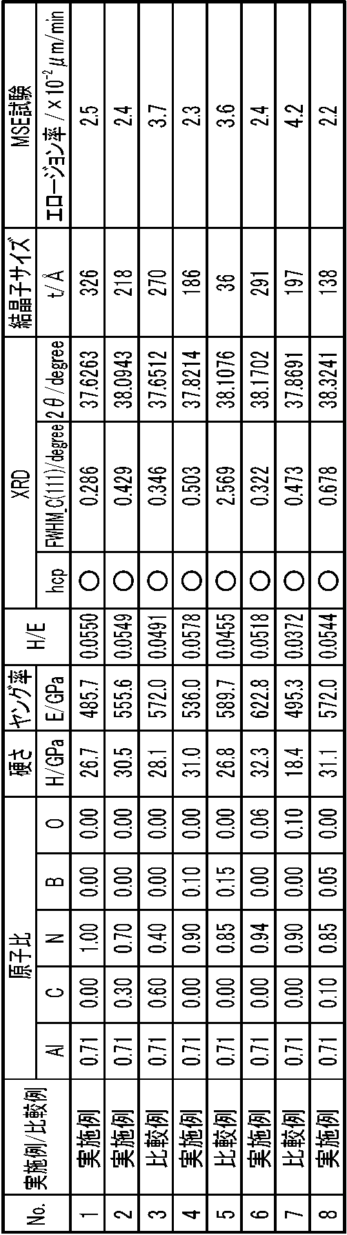
C含有量が0.5以上になると(No.3)、0.5未満の場合(No.2)に比べてエロージョン率が高くなり、耐摩耗性に劣った。これは、皮膜のヤング率が上がり、皮膜が割れ易くなったためであると考えられる。またB含有量が0.1を超えると(No.5)、結晶粒の微細化が進行し過ぎるため、0.1以下の場合(No.4)に比べて硬さが低下した。また半値幅(FWHM)が大きくなり、結晶粒ごと脱落し易くなったため、耐摩耗性に劣った。またO含有量が0.1以上の場合(No.7)、皮膜が軟化し過ぎるため、0.10未満の場合(No.6)に比べて耐摩耗性に劣った。
(実施例4)
C,B,Oの元素を含有する硬質皮膜20を成膜した点以外は、上記実施例1と同様である。上記実施例1において、成膜中の窒素ガスに、メタン(CH4)ガス、酸素(O)ガスを導入することにより、皮膜内にC、Oを添加した。またホウ素(B)は、ターゲット41に入れることにより添加した。Al含有量は77at%とし、基材11に印加するバイアス電圧は-100Vとした。硬質皮膜20の各評価方法は、上記実施例1と同様にした。試験結果を下記の表5に示す。
C,B,Oの元素を含有する硬質皮膜20を成膜した点以外は、上記実施例1と同様である。上記実施例1において、成膜中の窒素ガスに、メタン(CH4)ガス、酸素(O)ガスを導入することにより、皮膜内にC、Oを添加した。またホウ素(B)は、ターゲット41に入れることにより添加した。Al含有量は77at%とし、基材11に印加するバイアス電圧は-100Vとした。硬質皮膜20の各評価方法は、上記実施例1と同様にした。試験結果を下記の表5に示す。

C含有量が0.5以上である場合(No.5)に比べて、C含有量が0.5未満の場合(No.1~4)にはエロージョン率が低くなり、耐摩耗性が向上した。これは、皮膜の硬さ及びヤング率が共に下がり、皮膜が割れ難くなったためであると考えられる。またB含有量が0.1を超えると(No.8)、結晶粒の微細化が進行し過ぎるため、0.1以下の場合(No.6,7)に比べて硬さが低下した。また半値幅(FWHM)が大きくなり、結晶粒ごと脱落し易くなったため、耐摩耗性に劣った。またO含有量が0.1以上の場合(No.11)、皮膜が軟化し、耐摩耗性に劣った。
Claims (11)
- Al、Cr及びNを含有する硬質皮膜であって、
AlmCr1-mN1-x-y-zCxByOzの組成式からなり、
前記組成式において、mはAl、Crの合計に対するAlの原子比、1-mはAl、Crの合計に対するCrの原子比、1-x-y-zはN、C、B、Oの合計に対するNの原子比、xはN、C、B、Oの合計に対するCの原子比、yはN、C、B、Oの合計に対するBの原子比、zはN、C、B、Oの合計に対するOの原子比をそれぞれ示し、
0.68≦m≦0.85、y≦0.10の関係式が満たされており、
立方晶岩塩型の結晶構造を有し、
前記硬質皮膜の硬さをH(GPa)、前記硬質皮膜のヤング率をE(GPa)としたときに、ヤング率に対する硬さの比であるH/Eが0.050以上0.120以下であり且つHが20GPa以上であることを特徴とする、硬質皮膜。 - H/Eが0.058以上であることを特徴とする、請求項1に記載の硬質皮膜。
- CuKα線を用いたX線回折測定において、前記立方晶岩塩型の結晶構造の(111)面に基づくピークの半値幅が0.25°以上1.00°以下であることを特徴とする、請求項1又は2に記載の硬質皮膜。
- 前記半値幅が0.32°以上であることを特徴とする、請求項3に記載の硬質皮膜。
- Cの原子比xが0.05≦x<0.5の関係式を満たすことを特徴とする、請求項1、2又は4に記載の硬質皮膜。
- Bの原子比yが0.01≦y≦0.10の関係式を満たすことを特徴とする、請求項1、2又は4に記載の硬質皮膜。
- Oの原子比zが0<z<0.10の関係式を満たすことを特徴とする、請求項1、2又は4に記載の硬質皮膜。
- 基材と、
前記基材の表面に形成された請求項1、2又は4に記載の硬質皮膜と、を備えた、硬質皮膜被覆部材。 - AlmCr1-mN1-x-y-zCxByOzの組成式からなり、立方晶岩塩型の結晶構造を有する硬質皮膜を基材の表面に形成する硬質皮膜の製造方法であって、
前記組成式において、mはAl、Crの合計に対するAlの原子比、1-mはAl、Crの合計に対するCrの原子比、1-x-y-zはN、C、B、Oの合計に対するNの原子比、xはN、C、B、Oの合計に対するCの原子比、yはN、C、B、Oの合計に対するBの原子比、zはN、C、B、Oの合計に対するOの原子比をそれぞれ示し、
0.70<m≦0.85、y≦0.10の関係式が満たされており、
前記基材をステージ上に設置する工程と、
前記硬質皮膜の成分組成を有するターゲットを設置する工程と、
前記ターゲットを蒸発させることにより、前記基材の表面に前記硬質皮膜を成膜する工程と、を備え、
前記硬質皮膜を成膜する工程では、前記ステージから前記基材に印加するバイアス電圧Vが、-316≦V≦-214.3m+110の関係式を満たすように、前記基材にバイアス電圧を印加しつつ前記硬質皮膜を成膜することを特徴とする、硬質皮膜の製造方法。 - 前記バイアス電圧Vが、-1666m+1100≦V、の関係式を満たすことを特徴とする、請求項9に記載の硬質皮膜の製造方法。
- 前記硬質皮膜を成膜する工程において、前記ターゲットの放電面に対して垂直な方向に磁場を発生させることを特徴とする、請求項9又は10に記載の硬質皮膜の製造方法。
Applications Claiming Priority (4)
| Application Number | Priority Date | Filing Date | Title |
|---|---|---|---|
| JP2016062053A JP2017172022A (ja) | 2016-03-25 | 2016-03-25 | 硬質皮膜、硬質皮膜被覆部材及び硬質皮膜の製造方法 |
| JP2016-062053 | 2016-03-25 | ||
| JP2016196590A JP6789055B2 (ja) | 2016-10-04 | 2016-10-04 | 硬質皮膜、硬質皮膜被覆部材及び硬質皮膜の製造方法 |
| JP2016-196590 | 2016-10-04 |
Publications (1)
| Publication Number | Publication Date |
|---|---|
| WO2017163972A1 true WO2017163972A1 (ja) | 2017-09-28 |
Family
ID=59899432
Family Applications (1)
| Application Number | Title | Priority Date | Filing Date |
|---|---|---|---|
| PCT/JP2017/009922 Ceased WO2017163972A1 (ja) | 2016-03-25 | 2017-03-13 | 硬質皮膜、硬質皮膜被覆部材及び硬質皮膜の製造方法 |
Country Status (2)
| Country | Link |
|---|---|
| TW (1) | TW201804017A (ja) |
| WO (1) | WO2017163972A1 (ja) |
Cited By (4)
| Publication number | Priority date | Publication date | Assignee | Title |
|---|---|---|---|---|
| WO2020111122A1 (ja) * | 2018-11-29 | 2020-06-04 | 京セラ株式会社 | 被覆工具およびそれを備えた切削工具 |
| WO2020111123A1 (ja) * | 2018-11-29 | 2020-06-04 | 京セラ株式会社 | 被覆工具およびそれを備えた切削工具 |
| DE112021001965T5 (de) | 2020-03-27 | 2023-01-12 | Kyocera Corporation | Beschichtetes werkzeug |
| JP2023172378A (ja) * | 2022-05-23 | 2023-12-06 | 国立大学法人福井大学 | 固体材料の表面内部評価方法 |
Families Citing this family (1)
| Publication number | Priority date | Publication date | Assignee | Title |
|---|---|---|---|---|
| JP7378716B2 (ja) * | 2018-10-24 | 2023-11-14 | 日東電工株式会社 | エンドミルの製造方法 |
Citations (6)
| Publication number | Priority date | Publication date | Assignee | Title |
|---|---|---|---|---|
| JP2003071611A (ja) * | 2001-06-19 | 2003-03-12 | Kobe Steel Ltd | 切削工具用硬質皮膜およびその製造方法並びに硬質皮膜形成用ターゲット |
| JP2004268250A (ja) * | 2003-02-17 | 2004-09-30 | Hitachi Tool Engineering Ltd | 被覆エンドミル及び被覆用ターゲット |
| JP2005344148A (ja) * | 2004-06-01 | 2005-12-15 | Sumitomo Electric Ind Ltd | 耐摩耗性被膜およびこれを用いた表面被覆切削工具 |
| JP2006524748A (ja) * | 2003-04-28 | 2006-11-02 | ユナキス・バルツェルス・アクチェンゲゼルシャフト | AlCr含有の硬質材料層を有する工作物および製造方法 |
| WO2012173236A1 (ja) * | 2011-06-17 | 2012-12-20 | 株式会社神戸製鋼所 | 硬質皮膜被覆部材 |
| JP2014091169A (ja) * | 2012-10-31 | 2014-05-19 | Mitsubishi Materials Corp | 表面被覆切削工具 |
-
2017
- 2017-03-13 WO PCT/JP2017/009922 patent/WO2017163972A1/ja not_active Ceased
- 2017-03-22 TW TW106109570A patent/TW201804017A/zh unknown
Patent Citations (6)
| Publication number | Priority date | Publication date | Assignee | Title |
|---|---|---|---|---|
| JP2003071611A (ja) * | 2001-06-19 | 2003-03-12 | Kobe Steel Ltd | 切削工具用硬質皮膜およびその製造方法並びに硬質皮膜形成用ターゲット |
| JP2004268250A (ja) * | 2003-02-17 | 2004-09-30 | Hitachi Tool Engineering Ltd | 被覆エンドミル及び被覆用ターゲット |
| JP2006524748A (ja) * | 2003-04-28 | 2006-11-02 | ユナキス・バルツェルス・アクチェンゲゼルシャフト | AlCr含有の硬質材料層を有する工作物および製造方法 |
| JP2005344148A (ja) * | 2004-06-01 | 2005-12-15 | Sumitomo Electric Ind Ltd | 耐摩耗性被膜およびこれを用いた表面被覆切削工具 |
| WO2012173236A1 (ja) * | 2011-06-17 | 2012-12-20 | 株式会社神戸製鋼所 | 硬質皮膜被覆部材 |
| JP2014091169A (ja) * | 2012-10-31 | 2014-05-19 | Mitsubishi Materials Corp | 表面被覆切削工具 |
Cited By (17)
| Publication number | Priority date | Publication date | Assignee | Title |
|---|---|---|---|---|
| JP7213888B2 (ja) | 2018-11-29 | 2023-01-27 | 京セラ株式会社 | 被覆工具およびそれを備えた切削工具 |
| KR102591245B1 (ko) | 2018-11-29 | 2023-10-19 | 교세라 가부시키가이샤 | 피복 공구 및 그것을 구비한 절삭 공구 |
| KR20210087049A (ko) * | 2018-11-29 | 2021-07-09 | 교세라 가부시키가이샤 | 피복 공구 및 그것을 구비한 절삭 공구 |
| KR20210087478A (ko) * | 2018-11-29 | 2021-07-12 | 교세라 가부시키가이샤 | 피복 공구 및 그것을 구비한 절삭 공구 |
| CN113165082A (zh) * | 2018-11-29 | 2021-07-23 | 京瓷株式会社 | 涂层刀具及具备该涂层刀具的切削刀具 |
| JPWO2020111122A1 (ja) * | 2018-11-29 | 2021-10-07 | 京セラ株式会社 | 被覆工具およびそれを備えた切削工具 |
| JPWO2020111123A1 (ja) * | 2018-11-29 | 2021-10-07 | 京セラ株式会社 | 被覆工具およびそれを備えた切削工具 |
| CN113165082B (zh) * | 2018-11-29 | 2025-02-21 | 京瓷株式会社 | 涂层刀具及具备该涂层刀具的切削刀具 |
| WO2020111123A1 (ja) * | 2018-11-29 | 2020-06-04 | 京セラ株式会社 | 被覆工具およびそれを備えた切削工具 |
| US12151289B2 (en) | 2018-11-29 | 2024-11-26 | Kyocera Corporation | Coated tool and cutting tool including same |
| WO2020111122A1 (ja) * | 2018-11-29 | 2020-06-04 | 京セラ株式会社 | 被覆工具およびそれを備えた切削工具 |
| KR102676439B1 (ko) * | 2018-11-29 | 2024-06-19 | 교세라 가부시키가이샤 | 피복 공구 및 그것을 구비한 절삭 공구 |
| JP7441177B2 (ja) | 2018-11-29 | 2024-02-29 | 京セラ株式会社 | 被覆工具およびそれを備えた切削工具 |
| DE112021001965T5 (de) | 2020-03-27 | 2023-01-12 | Kyocera Corporation | Beschichtetes werkzeug |
| US12454012B2 (en) | 2020-03-27 | 2025-10-28 | Kyocera Corporation | Coated tool |
| JP7399504B2 (ja) | 2022-05-23 | 2023-12-18 | 国立大学法人福井大学 | 固体材料の表面内部評価方法 |
| JP2023172378A (ja) * | 2022-05-23 | 2023-12-06 | 国立大学法人福井大学 | 固体材料の表面内部評価方法 |
Also Published As
| Publication number | Publication date |
|---|---|
| TW201804017A (zh) | 2018-02-01 |
Similar Documents
| Publication | Publication Date | Title |
|---|---|---|
| JP6789055B2 (ja) | 硬質皮膜、硬質皮膜被覆部材及び硬質皮膜の製造方法 | |
| JP6268530B2 (ja) | 硬質被覆層がすぐれた耐チッピング性を発揮する表面被覆切削工具 | |
| CN106102972B (zh) | 被覆切削工具和其制造方法 | |
| JP5187570B2 (ja) | 硬質被覆層がすぐれた耐摩耗性を発揮する表面被覆切削工具 | |
| JP5621881B2 (ja) | 硬質皮膜被覆工具 | |
| WO2017163972A1 (ja) | 硬質皮膜、硬質皮膜被覆部材及び硬質皮膜の製造方法 | |
| JP2011189419A (ja) | 耐摩耗性に優れた被覆工具 | |
| WO2014132512A1 (ja) | 切削工具 | |
| WO2014084338A1 (ja) | 表面被覆切削工具 | |
| EP4292735A1 (en) | Coated tool | |
| JP2016032861A (ja) | 被覆工具 | |
| WO2014142190A1 (ja) | 硬質皮膜、硬質皮膜被覆部材、及びそれらの製造方法 | |
| WO2021167087A1 (ja) | 被覆工具 | |
| JP2017172022A (ja) | 硬質皮膜、硬質皮膜被覆部材及び硬質皮膜の製造方法 | |
| Lu et al. | Characterization and wear role of (CrAlVTiNb) Nx high-entropy alloy nitride films deposited by high power impulse magnetron sputtering | |
| KR20130028080A (ko) | 절삭 공구 | |
| CN108349016A (zh) | 表面包覆切削工具 | |
| JP6789503B2 (ja) | 硬質皮膜の成膜方法 | |
| JP6387190B2 (ja) | 被膜 | |
| JP5660457B2 (ja) | 硬質皮膜被覆金型 | |
| JP2015157975A (ja) | 硬質皮膜およびその形成方法 | |
| Yang et al. | Microstructure and mechanical properties of W–Ni–N coatings prepared by magnetron sputtering | |
| EP4082699B1 (en) | Coated cutting tool | |
| JP5617933B2 (ja) | 硬質皮膜被覆工具及びその製造方法 | |
| JP5240666B2 (ja) | すぐれた切屑排出性を示す表面被覆切削工具 |
Legal Events
| Date | Code | Title | Description |
|---|---|---|---|
| NENP | Non-entry into the national phase |
Ref country code: DE |
|
| 121 | Ep: the epo has been informed by wipo that ep was designated in this application |
Ref document number: 17770015 Country of ref document: EP Kind code of ref document: A1 |
|
| 122 | Ep: pct application non-entry in european phase |
Ref document number: 17770015 Country of ref document: EP Kind code of ref document: A1 |