WO2017163971A1 - Supporting sheet and composite sheet for protective film formation - Google Patents
Supporting sheet and composite sheet for protective film formation Download PDFInfo
- Publication number
- WO2017163971A1 WO2017163971A1 PCT/JP2017/009921 JP2017009921W WO2017163971A1 WO 2017163971 A1 WO2017163971 A1 WO 2017163971A1 JP 2017009921 W JP2017009921 W JP 2017009921W WO 2017163971 A1 WO2017163971 A1 WO 2017163971A1
- Authority
- WO
- WIPO (PCT)
- Prior art keywords
- protective film
- forming
- adhesive layer
- film
- meth
- Prior art date
Links
- 230000001681 protective effect Effects 0.000 title claims abstract description 473
- 239000002131 composite material Substances 0.000 title claims abstract description 169
- 230000015572 biosynthetic process Effects 0.000 title abstract description 83
- 239000012790 adhesive layer Substances 0.000 claims abstract description 126
- 230000003746 surface roughness Effects 0.000 claims abstract description 119
- 239000000463 material Substances 0.000 claims description 209
- 239000010410 layer Substances 0.000 claims description 208
- 239000004820 Pressure-sensitive adhesive Substances 0.000 claims description 169
- 239000000758 substrate Substances 0.000 claims description 68
- 239000000853 adhesive Substances 0.000 abstract description 26
- 230000001070 adhesive effect Effects 0.000 abstract description 26
- 239000002585 base Substances 0.000 description 187
- 239000000203 mixture Substances 0.000 description 156
- NIXOWILDQLNWCW-UHFFFAOYSA-M Acrylate Chemical compound [O-]C(=O)C=C NIXOWILDQLNWCW-UHFFFAOYSA-M 0.000 description 149
- 229920001187 thermosetting polymer Polymers 0.000 description 136
- -1 2-ethylhexyl Chemical group 0.000 description 71
- 239000004065 semiconductor Substances 0.000 description 71
- 150000001875 compounds Chemical class 0.000 description 68
- 238000000034 method Methods 0.000 description 66
- 229920000642 polymer Polymers 0.000 description 64
- 238000004519 manufacturing process Methods 0.000 description 58
- 239000000178 monomer Substances 0.000 description 45
- 125000000524 functional group Chemical group 0.000 description 42
- 239000003431 cross linking reagent Substances 0.000 description 41
- 239000000975 dye Substances 0.000 description 39
- CERQOIWHTDAKMF-UHFFFAOYSA-N Methacrylic acid Chemical compound CC(=C)C(O)=O CERQOIWHTDAKMF-UHFFFAOYSA-N 0.000 description 36
- 239000003822 epoxy resin Substances 0.000 description 35
- 229920000647 polyepoxide Polymers 0.000 description 35
- 235000012431 wafers Nutrition 0.000 description 35
- 229920005989 resin Polymers 0.000 description 33
- 239000011347 resin Substances 0.000 description 33
- 239000002904 solvent Substances 0.000 description 32
- ZWEHNKRNPOVVGH-UHFFFAOYSA-N 2-Butanone Chemical compound CCC(C)=O ZWEHNKRNPOVVGH-UHFFFAOYSA-N 0.000 description 30
- NIXOWILDQLNWCW-UHFFFAOYSA-N acrylic acid group Chemical group C(C=C)(=O)O NIXOWILDQLNWCW-UHFFFAOYSA-N 0.000 description 30
- 239000004925 Acrylic resin Substances 0.000 description 28
- 229920000178 Acrylic resin Polymers 0.000 description 28
- 239000003795 chemical substances by application Substances 0.000 description 27
- 125000002887 hydroxy group Chemical group [H]O* 0.000 description 26
- 229920000058 polyacrylate Polymers 0.000 description 26
- 238000002156 mixing Methods 0.000 description 25
- XUIMIQQOPSSXEZ-UHFFFAOYSA-N Silicon Chemical compound [Si] XUIMIQQOPSSXEZ-UHFFFAOYSA-N 0.000 description 23
- 229910052710 silicon Inorganic materials 0.000 description 22
- 239000010703 silicon Substances 0.000 description 22
- 239000003086 colorant Substances 0.000 description 20
- 239000000470 constituent Substances 0.000 description 20
- 239000000945 filler Substances 0.000 description 20
- 238000010030 laminating Methods 0.000 description 20
- 125000003277 amino group Chemical group 0.000 description 19
- 239000007822 coupling agent Substances 0.000 description 19
- 238000007689 inspection Methods 0.000 description 19
- 230000000903 blocking effect Effects 0.000 description 18
- 238000013329 compounding Methods 0.000 description 18
- 238000007648 laser printing Methods 0.000 description 18
- 150000002430 hydrocarbons Chemical group 0.000 description 17
- 238000003860 storage Methods 0.000 description 16
- 229930195735 unsaturated hydrocarbon Natural products 0.000 description 15
- 239000003999 initiator Substances 0.000 description 14
- 230000008569 process Effects 0.000 description 14
- 239000002994 raw material Substances 0.000 description 14
- 239000004593 Epoxy Substances 0.000 description 12
- 125000003647 acryloyl group Chemical group O=C([*])C([H])=C([H])[H] 0.000 description 12
- 125000003178 carboxy group Chemical group [H]OC(*)=O 0.000 description 12
- 239000005011 phenolic resin Substances 0.000 description 12
- 239000004743 Polypropylene Substances 0.000 description 11
- 230000000694 effects Effects 0.000 description 11
- 229920001155 polypropylene Polymers 0.000 description 11
- ATUOYWHBWRKTHZ-UHFFFAOYSA-N Propane Chemical compound CCC ATUOYWHBWRKTHZ-UHFFFAOYSA-N 0.000 description 10
- 239000000654 additive Substances 0.000 description 10
- 230000000996 additive effect Effects 0.000 description 10
- 230000000052 comparative effect Effects 0.000 description 9
- 239000012948 isocyanate Substances 0.000 description 9
- IQPQWNKOIGAROB-UHFFFAOYSA-N isocyanate group Chemical group [N-]=C=O IQPQWNKOIGAROB-UHFFFAOYSA-N 0.000 description 9
- LYCAIKOWRPUZTN-UHFFFAOYSA-N Ethylene glycol Chemical compound OCCO LYCAIKOWRPUZTN-UHFFFAOYSA-N 0.000 description 8
- PPBRXRYQALVLMV-UHFFFAOYSA-N Styrene Chemical compound C=CC1=CC=CC=C1 PPBRXRYQALVLMV-UHFFFAOYSA-N 0.000 description 8
- 150000001252 acrylic acid derivatives Chemical class 0.000 description 8
- 125000003118 aryl group Chemical group 0.000 description 8
- IISBACLAFKSPIT-UHFFFAOYSA-N bisphenol A Chemical compound C=1C=C(O)C=CC=1C(C)(C)C1=CC=C(O)C=C1 IISBACLAFKSPIT-UHFFFAOYSA-N 0.000 description 8
- 125000004435 hydrogen atom Chemical group [H]* 0.000 description 8
- 239000007787 solid Substances 0.000 description 8
- 239000002253 acid Substances 0.000 description 7
- 229920006223 adhesive resin Polymers 0.000 description 7
- 238000001035 drying Methods 0.000 description 7
- 125000003700 epoxy group Chemical group 0.000 description 7
- 238000010438 heat treatment Methods 0.000 description 7
- 239000011256 inorganic filler Substances 0.000 description 7
- 229910003475 inorganic filler Inorganic materials 0.000 description 7
- 239000005056 polyisocyanate Substances 0.000 description 7
- 229920001228 polyisocyanate Polymers 0.000 description 7
- 229920005992 thermoplastic resin Polymers 0.000 description 7
- VYPSYNLAJGMNEJ-UHFFFAOYSA-N Silicium dioxide Chemical compound O=[Si]=O VYPSYNLAJGMNEJ-UHFFFAOYSA-N 0.000 description 6
- 239000004840 adhesive resin Substances 0.000 description 6
- 238000011156 evaluation Methods 0.000 description 6
- LNEPOXFFQSENCJ-UHFFFAOYSA-N haloperidol Chemical compound C1CC(O)(C=2C=CC(Cl)=CC=2)CCN1CCCC(=O)C1=CC=C(F)C=C1 LNEPOXFFQSENCJ-UHFFFAOYSA-N 0.000 description 6
- 125000001421 myristyl group Chemical group [H]C([*])([H])C([H])([H])C([H])([H])C([H])([H])C([H])([H])C([H])([H])C([H])([H])C([H])([H])C([H])([H])C([H])([H])C([H])([H])C([H])([H])C([H])([H])C([H])([H])[H] 0.000 description 6
- 125000000913 palmityl group Chemical group [H]C([*])([H])C([H])([H])C([H])([H])C([H])([H])C([H])([H])C([H])([H])C([H])([H])C([H])([H])C([H])([H])C([H])([H])C([H])([H])C([H])([H])C([H])([H])C([H])([H])C([H])([H])C([H])([H])[H] 0.000 description 6
- WXZMFSXDPGVJKK-UHFFFAOYSA-N pentaerythritol Chemical compound OCC(CO)(CO)CO WXZMFSXDPGVJKK-UHFFFAOYSA-N 0.000 description 6
- ISWSIDIOOBJBQZ-UHFFFAOYSA-N phenol group Chemical group C1(=CC=CC=C1)O ISWSIDIOOBJBQZ-UHFFFAOYSA-N 0.000 description 6
- 238000006116 polymerization reaction Methods 0.000 description 6
- 125000004079 stearyl group Chemical group [H]C([*])([H])C([H])([H])C([H])([H])C([H])([H])C([H])([H])C([H])([H])C([H])([H])C([H])([H])C([H])([H])C([H])([H])C([H])([H])C([H])([H])C([H])([H])C([H])([H])C([H])([H])C([H])([H])C([H])([H])C([H])([H])[H] 0.000 description 6
- ISAOCJYIOMOJEB-UHFFFAOYSA-N benzoin Chemical compound C=1C=CC=CC=1C(O)C(=O)C1=CC=CC=C1 ISAOCJYIOMOJEB-UHFFFAOYSA-N 0.000 description 5
- 238000006243 chemical reaction Methods 0.000 description 5
- 239000011248 coating agent Substances 0.000 description 5
- 238000000576 coating method Methods 0.000 description 5
- 150000002148 esters Chemical class 0.000 description 5
- 230000009477 glass transition Effects 0.000 description 5
- ZXEKIIBDNHEJCQ-UHFFFAOYSA-N isobutanol Chemical compound CC(C)CO ZXEKIIBDNHEJCQ-UHFFFAOYSA-N 0.000 description 5
- 229940059574 pentaerithrityl Drugs 0.000 description 5
- 125000001997 phenyl group Chemical group [H]C1=C([H])C([H])=C(*)C([H])=C1[H] 0.000 description 5
- 238000007639 printing Methods 0.000 description 5
- 239000001294 propane Substances 0.000 description 5
- 238000012360 testing method Methods 0.000 description 5
- DVKJHBMWWAPEIU-UHFFFAOYSA-N toluene 2,4-diisocyanate Chemical compound CC1=CC=C(N=C=O)C=C1N=C=O DVKJHBMWWAPEIU-UHFFFAOYSA-N 0.000 description 5
- 125000000391 vinyl group Chemical group [H]C([*])=C([H])[H] 0.000 description 5
- HECLRDQVFMWTQS-RGOKHQFPSA-N 1755-01-7 Chemical compound C1[C@H]2[C@@H]3CC=C[C@@H]3[C@@H]1C=C2 HECLRDQVFMWTQS-RGOKHQFPSA-N 0.000 description 4
- JAHNSTQSQJOJLO-UHFFFAOYSA-N 2-(3-fluorophenyl)-1h-imidazole Chemical compound FC1=CC=CC(C=2NC=CN=2)=C1 JAHNSTQSQJOJLO-UHFFFAOYSA-N 0.000 description 4
- TXBCBTDQIULDIA-UHFFFAOYSA-N 2-[[3-hydroxy-2,2-bis(hydroxymethyl)propoxy]methyl]-2-(hydroxymethyl)propane-1,3-diol Chemical compound OCC(CO)(CO)COCC(CO)(CO)CO TXBCBTDQIULDIA-UHFFFAOYSA-N 0.000 description 4
- CSCPPACGZOOCGX-UHFFFAOYSA-N Acetone Chemical compound CC(C)=O CSCPPACGZOOCGX-UHFFFAOYSA-N 0.000 description 4
- KWOLFJPFCHCOCG-UHFFFAOYSA-N Acetophenone Chemical compound CC(=O)C1=CC=CC=C1 KWOLFJPFCHCOCG-UHFFFAOYSA-N 0.000 description 4
- XYFCBTPGUUZFHI-UHFFFAOYSA-N Phosphine Chemical compound P XYFCBTPGUUZFHI-UHFFFAOYSA-N 0.000 description 4
- ZJCCRDAZUWHFQH-UHFFFAOYSA-N Trimethylolpropane Chemical compound CCC(CO)(CO)CO ZJCCRDAZUWHFQH-UHFFFAOYSA-N 0.000 description 4
- XTXRWKRVRITETP-UHFFFAOYSA-N Vinyl acetate Chemical compound CC(=O)OC=C XTXRWKRVRITETP-UHFFFAOYSA-N 0.000 description 4
- 125000000217 alkyl group Chemical group 0.000 description 4
- QGBSISYHAICWAH-UHFFFAOYSA-N dicyandiamide Chemical compound NC(N)=NC#N QGBSISYHAICWAH-UHFFFAOYSA-N 0.000 description 4
- 238000007865 diluting Methods 0.000 description 4
- 125000003438 dodecyl group Chemical group [H]C([H])([H])C([H])([H])C([H])([H])C([H])([H])C([H])([H])C([H])([H])C([H])([H])C([H])([H])C([H])([H])C([H])([H])C([H])([H])C([H])([H])* 0.000 description 4
- 125000003055 glycidyl group Chemical group C(C1CO1)* 0.000 description 4
- 238000000227 grinding Methods 0.000 description 4
- 238000009499 grossing Methods 0.000 description 4
- RBQRWNWVPQDTJJ-UHFFFAOYSA-N methacryloyloxyethyl isocyanate Chemical compound CC(=C)C(=O)OCCN=C=O RBQRWNWVPQDTJJ-UHFFFAOYSA-N 0.000 description 4
- LVHBHZANLOWSRM-UHFFFAOYSA-N methylenebutanedioic acid Natural products OC(=O)CC(=C)C(O)=O LVHBHZANLOWSRM-UHFFFAOYSA-N 0.000 description 4
- 229920000139 polyethylene terephthalate Polymers 0.000 description 4
- 239000005020 polyethylene terephthalate Substances 0.000 description 4
- 230000000379 polymerizing effect Effects 0.000 description 4
- 239000002356 single layer Substances 0.000 description 4
- 239000000126 substance Substances 0.000 description 4
- 229920002803 thermoplastic polyurethane Polymers 0.000 description 4
- 238000002834 transmittance Methods 0.000 description 4
- RIOQSEWOXXDEQQ-UHFFFAOYSA-N triphenylphosphine Chemical compound C1=CC=CC=C1P(C=1C=CC=CC=1)C1=CC=CC=C1 RIOQSEWOXXDEQQ-UHFFFAOYSA-N 0.000 description 4
- 125000000954 2-hydroxyethyl group Chemical group [H]C([*])([H])C([H])([H])O[H] 0.000 description 3
- SXIFAEWFOJETOA-UHFFFAOYSA-N 4-hydroxy-butyl Chemical group [CH2]CCCO SXIFAEWFOJETOA-UHFFFAOYSA-N 0.000 description 3
- SNRUBQQJIBEYMU-UHFFFAOYSA-N Dodecane Natural products CCCCCCCCCCCC SNRUBQQJIBEYMU-UHFFFAOYSA-N 0.000 description 3
- LFQSCWFLJHTTHZ-UHFFFAOYSA-N Ethanol Chemical compound CCO LFQSCWFLJHTTHZ-UHFFFAOYSA-N 0.000 description 3
- XEKOWRVHYACXOJ-UHFFFAOYSA-N Ethyl acetate Chemical compound CCOC(C)=O XEKOWRVHYACXOJ-UHFFFAOYSA-N 0.000 description 3
- KFZMGEQAYNKOFK-UHFFFAOYSA-N Isopropanol Chemical compound CC(C)O KFZMGEQAYNKOFK-UHFFFAOYSA-N 0.000 description 3
- OKKJLVBELUTLKV-UHFFFAOYSA-N Methanol Chemical compound OC OKKJLVBELUTLKV-UHFFFAOYSA-N 0.000 description 3
- ZMXDDKWLCZADIW-UHFFFAOYSA-N N,N-Dimethylformamide Chemical compound CN(C)C=O ZMXDDKWLCZADIW-UHFFFAOYSA-N 0.000 description 3
- LRHPLDYGYMQRHN-UHFFFAOYSA-N N-Butanol Chemical compound CCCCO LRHPLDYGYMQRHN-UHFFFAOYSA-N 0.000 description 3
- DNIAPMSPPWPWGF-UHFFFAOYSA-N Propylene glycol Chemical compound CC(O)CO DNIAPMSPPWPWGF-UHFFFAOYSA-N 0.000 description 3
- 239000006087 Silane Coupling Agent Substances 0.000 description 3
- YXFVVABEGXRONW-UHFFFAOYSA-N Toluene Chemical compound CC1=CC=CC=C1 YXFVVABEGXRONW-UHFFFAOYSA-N 0.000 description 3
- 125000001931 aliphatic group Chemical group 0.000 description 3
- 125000005907 alkyl ester group Chemical group 0.000 description 3
- 125000004432 carbon atom Chemical group C* 0.000 description 3
- 229920001577 copolymer Polymers 0.000 description 3
- 238000004132 cross linking Methods 0.000 description 3
- 125000002704 decyl group Chemical group [H]C([H])([H])C([H])([H])C([H])([H])C([H])([H])C([H])([H])C([H])([H])C([H])([H])C([H])([H])C([H])([H])C([H])([H])* 0.000 description 3
- 150000001991 dicarboxylic acids Chemical class 0.000 description 3
- MTHSVFCYNBDYFN-UHFFFAOYSA-N diethylene glycol Chemical compound OCCOCCO MTHSVFCYNBDYFN-UHFFFAOYSA-N 0.000 description 3
- ZUOUZKKEUPVFJK-UHFFFAOYSA-N diphenyl Chemical class C1=CC=CC=C1C1=CC=CC=C1 ZUOUZKKEUPVFJK-UHFFFAOYSA-N 0.000 description 3
- 229920001971 elastomer Polymers 0.000 description 3
- 238000010894 electron beam technology Methods 0.000 description 3
- 125000001495 ethyl group Chemical group [H]C([H])([H])C([H])([H])* 0.000 description 3
- 125000004051 hexyl group Chemical group [H]C([H])([H])C([H])([H])C([H])([H])C([H])([H])C([H])([H])C([H])([H])* 0.000 description 3
- 125000004029 hydroxymethyl group Chemical group [H]OC([H])([H])* 0.000 description 3
- 230000001788 irregular Effects 0.000 description 3
- 125000000959 isobutyl group Chemical group [H]C([H])([H])C([H])(C([H])([H])[H])C([H])([H])* 0.000 description 3
- ZFSLODLOARCGLH-UHFFFAOYSA-N isocyanuric acid Chemical compound OC1=NC(O)=NC(O)=N1 ZFSLODLOARCGLH-UHFFFAOYSA-N 0.000 description 3
- 125000001449 isopropyl group Chemical group [H]C([H])([H])C([H])(*)C([H])([H])[H] 0.000 description 3
- 238000005259 measurement Methods 0.000 description 3
- 239000000434 metal complex dye Substances 0.000 description 3
- 125000002496 methyl group Chemical group [H]C([H])([H])* 0.000 description 3
- 125000004123 n-propyl group Chemical group [H]C([H])([H])C([H])([H])C([H])([H])* 0.000 description 3
- 239000002245 particle Substances 0.000 description 3
- 125000002958 pentadecyl group Chemical group [H]C([*])([H])C([H])([H])C([H])([H])C([H])([H])C([H])([H])C([H])([H])C([H])([H])C([H])([H])C([H])([H])C([H])([H])C([H])([H])C([H])([H])C([H])([H])C([H])([H])C([H])([H])[H] 0.000 description 3
- 125000001147 pentyl group Chemical group C(CCCC)* 0.000 description 3
- 229920006287 phenoxy resin Polymers 0.000 description 3
- 239000013034 phenoxy resin Substances 0.000 description 3
- 239000000049 pigment Substances 0.000 description 3
- 229920000728 polyester Polymers 0.000 description 3
- 229920005862 polyol Polymers 0.000 description 3
- 238000012545 processing Methods 0.000 description 3
- 238000007788 roughening Methods 0.000 description 3
- 239000005060 rubber Substances 0.000 description 3
- 125000002914 sec-butyl group Chemical group [H]C([H])([H])C([H])([H])C([H])(*)C([H])([H])[H] 0.000 description 3
- 239000000377 silicon dioxide Substances 0.000 description 3
- 229910001220 stainless steel Inorganic materials 0.000 description 3
- 239000010935 stainless steel Substances 0.000 description 3
- 238000003756 stirring Methods 0.000 description 3
- 230000001629 suppression Effects 0.000 description 3
- 125000000999 tert-butyl group Chemical group [H]C([H])([H])C(*)(C([H])([H])[H])C([H])([H])[H] 0.000 description 3
- 239000011800 void material Substances 0.000 description 3
- FKTHNVSLHLHISI-UHFFFAOYSA-N 1,2-bis(isocyanatomethyl)benzene Chemical compound O=C=NCC1=CC=CC=C1CN=C=O FKTHNVSLHLHISI-UHFFFAOYSA-N 0.000 description 2
- 239000012956 1-hydroxycyclohexylphenyl-ketone Substances 0.000 description 2
- OZAIFHULBGXAKX-UHFFFAOYSA-N 2-(2-cyanopropan-2-yldiazenyl)-2-methylpropanenitrile Chemical compound N#CC(C)(C)N=NC(C)(C)C#N OZAIFHULBGXAKX-UHFFFAOYSA-N 0.000 description 2
- GOXQRTZXKQZDDN-UHFFFAOYSA-N 2-Ethylhexyl acrylate Chemical compound CCCCC(CC)COC(=O)C=C GOXQRTZXKQZDDN-UHFFFAOYSA-N 0.000 description 2
- 125000003903 2-propenyl group Chemical group [H]C([*])([H])C([H])=C([H])[H] 0.000 description 2
- QOXOZONBQWIKDA-UHFFFAOYSA-N 3-hydroxypropyl Chemical group [CH2]CCO QOXOZONBQWIKDA-UHFFFAOYSA-N 0.000 description 2
- HRPVXLWXLXDGHG-UHFFFAOYSA-N Acrylamide Chemical group NC(=O)C=C HRPVXLWXLXDGHG-UHFFFAOYSA-N 0.000 description 2
- NLHHRLWOUZZQLW-UHFFFAOYSA-N Acrylonitrile Chemical compound C=CC#N NLHHRLWOUZZQLW-UHFFFAOYSA-N 0.000 description 2
- GAWIXWVDTYZWAW-UHFFFAOYSA-N C[CH]O Chemical group C[CH]O GAWIXWVDTYZWAW-UHFFFAOYSA-N 0.000 description 2
- VTYYLEPIZMXCLO-UHFFFAOYSA-L Calcium carbonate Chemical compound [Ca+2].[O-]C([O-])=O VTYYLEPIZMXCLO-UHFFFAOYSA-L 0.000 description 2
- VGGSQFUCUMXWEO-UHFFFAOYSA-N Ethene Chemical compound C=C VGGSQFUCUMXWEO-UHFFFAOYSA-N 0.000 description 2
- JOYRKODLDBILNP-UHFFFAOYSA-N Ethyl urethane Chemical compound CCOC(N)=O JOYRKODLDBILNP-UHFFFAOYSA-N 0.000 description 2
- 239000005977 Ethylene Substances 0.000 description 2
- VZCYOOQTPOCHFL-OWOJBTEDSA-N Fumaric acid Chemical compound OC(=O)\C=C\C(O)=O VZCYOOQTPOCHFL-OWOJBTEDSA-N 0.000 description 2
- 239000005057 Hexamethylene diisocyanate Substances 0.000 description 2
- UFHFLCQGNIYNRP-UHFFFAOYSA-N Hydrogen Chemical compound [H][H] UFHFLCQGNIYNRP-UHFFFAOYSA-N 0.000 description 2
- XEEYBQQBJWHFJM-UHFFFAOYSA-N Iron Chemical compound [Fe] XEEYBQQBJWHFJM-UHFFFAOYSA-N 0.000 description 2
- BAPJBEWLBFYGME-UHFFFAOYSA-N Methyl acrylate Chemical compound COC(=O)C=C BAPJBEWLBFYGME-UHFFFAOYSA-N 0.000 description 2
- CNCOEDDPFOAUMB-UHFFFAOYSA-N N-Methylolacrylamide Chemical compound OCNC(=O)C=C CNCOEDDPFOAUMB-UHFFFAOYSA-N 0.000 description 2
- 239000002202 Polyethylene glycol Substances 0.000 description 2
- 239000004642 Polyimide Substances 0.000 description 2
- 239000004793 Polystyrene Substances 0.000 description 2
- KAESVJOAVNADME-UHFFFAOYSA-N Pyrrole Chemical compound C=1C=CNC=1 KAESVJOAVNADME-UHFFFAOYSA-N 0.000 description 2
- 235000000126 Styrax benzoin Nutrition 0.000 description 2
- 244000028419 Styrax benzoin Species 0.000 description 2
- 235000008411 Sumatra benzointree Nutrition 0.000 description 2
- WYURNTSHIVDZCO-UHFFFAOYSA-N Tetrahydrofuran Chemical compound C1CCOC1 WYURNTSHIVDZCO-UHFFFAOYSA-N 0.000 description 2
- UUQQGGWZVKUCBD-UHFFFAOYSA-N [4-(hydroxymethyl)-2-phenyl-1h-imidazol-5-yl]methanol Chemical compound N1C(CO)=C(CO)N=C1C1=CC=CC=C1 UUQQGGWZVKUCBD-UHFFFAOYSA-N 0.000 description 2
- 238000010521 absorption reaction Methods 0.000 description 2
- 125000002723 alicyclic group Chemical group 0.000 description 2
- 150000001336 alkenes Chemical class 0.000 description 2
- PNEYBMLMFCGWSK-UHFFFAOYSA-N aluminium oxide Inorganic materials [O-2].[O-2].[O-2].[Al+3].[Al+3] PNEYBMLMFCGWSK-UHFFFAOYSA-N 0.000 description 2
- 150000001412 amines Chemical class 0.000 description 2
- 125000003710 aryl alkyl group Chemical group 0.000 description 2
- FFBZKUHRIXKOSY-UHFFFAOYSA-N aziridine-1-carboxamide Chemical compound NC(=O)N1CC1 FFBZKUHRIXKOSY-UHFFFAOYSA-N 0.000 description 2
- 239000000987 azo dye Substances 0.000 description 2
- 230000001588 bifunctional effect Effects 0.000 description 2
- MQDJYUACMFCOFT-UHFFFAOYSA-N bis[2-(1-hydroxycyclohexyl)phenyl]methanone Chemical compound C=1C=CC=C(C(=O)C=2C(=CC=CC=2)C2(O)CCCCC2)C=1C1(O)CCCCC1 MQDJYUACMFCOFT-UHFFFAOYSA-N 0.000 description 2
- PXKLMJQFEQBVLD-UHFFFAOYSA-N bisphenol F Chemical compound C1=CC(O)=CC=C1CC1=CC=C(O)C=C1 PXKLMJQFEQBVLD-UHFFFAOYSA-N 0.000 description 2
- CQEYYJKEWSMYFG-UHFFFAOYSA-N butyl acrylate Chemical compound CCCCOC(=O)C=C CQEYYJKEWSMYFG-UHFFFAOYSA-N 0.000 description 2
- 239000006229 carbon black Substances 0.000 description 2
- 239000013522 chelant Substances 0.000 description 2
- 238000007334 copolymerization reaction Methods 0.000 description 2
- 230000007797 corrosion Effects 0.000 description 2
- 238000005260 corrosion Methods 0.000 description 2
- 125000006841 cyclic skeleton Chemical group 0.000 description 2
- PESYEWKSBIWTAK-UHFFFAOYSA-N cyclopenta-1,3-diene;titanium(2+) Chemical class [Ti+2].C=1C=C[CH-]C=1.C=1C=C[CH-]C=1 PESYEWKSBIWTAK-UHFFFAOYSA-N 0.000 description 2
- 230000007547 defect Effects 0.000 description 2
- PPSZHCXTGRHULJ-UHFFFAOYSA-N dioxazine Chemical compound O1ON=CC=C1 PPSZHCXTGRHULJ-UHFFFAOYSA-N 0.000 description 2
- 238000004049 embossing Methods 0.000 description 2
- RJLZSKYNYLYCNY-UHFFFAOYSA-N ethyl carbamate;isocyanic acid Chemical group N=C=O.CCOC(N)=O RJLZSKYNYLYCNY-UHFFFAOYSA-N 0.000 description 2
- 239000007789 gas Substances 0.000 description 2
- 238000005227 gel permeation chromatography Methods 0.000 description 2
- 235000019382 gum benzoic Nutrition 0.000 description 2
- 125000003187 heptyl group Chemical group [H]C([*])([H])C([H])([H])C([H])([H])C([H])([H])C([H])([H])C([H])([H])C([H])([H])[H] 0.000 description 2
- RRAMGCGOFNQTLD-UHFFFAOYSA-N hexamethylene diisocyanate Chemical compound O=C=NCCCCCCN=C=O RRAMGCGOFNQTLD-UHFFFAOYSA-N 0.000 description 2
- 229910052739 hydrogen Inorganic materials 0.000 description 2
- 239000001257 hydrogen Substances 0.000 description 2
- RAXXELZNTBOGNW-UHFFFAOYSA-N imidazole Natural products C1=CNC=N1 RAXXELZNTBOGNW-UHFFFAOYSA-N 0.000 description 2
- 150000002466 imines Chemical class 0.000 description 2
- 239000004615 ingredient Substances 0.000 description 2
- 239000001023 inorganic pigment Substances 0.000 description 2
- 230000001678 irradiating effect Effects 0.000 description 2
- 125000002960 margaryl group Chemical group [H]C([*])([H])C([H])([H])C([H])([H])C([H])([H])C([H])([H])C([H])([H])C([H])([H])C([H])([H])C([H])([H])C([H])([H])C([H])([H])C([H])([H])C([H])([H])C([H])([H])C([H])([H])C([H])([H])C([H])([H])[H] 0.000 description 2
- 229910052751 metal Inorganic materials 0.000 description 2
- 239000002184 metal Substances 0.000 description 2
- 150000002763 monocarboxylic acids Chemical class 0.000 description 2
- KBJFYLLAMSZSOG-UHFFFAOYSA-N n-(3-trimethoxysilylpropyl)aniline Chemical compound CO[Si](OC)(OC)CCCNC1=CC=CC=C1 KBJFYLLAMSZSOG-UHFFFAOYSA-N 0.000 description 2
- SLCVBVWXLSEKPL-UHFFFAOYSA-N neopentyl glycol Chemical compound OCC(C)(C)CO SLCVBVWXLSEKPL-UHFFFAOYSA-N 0.000 description 2
- JFNLZVQOOSMTJK-KNVOCYPGSA-N norbornene Chemical compound C1[C@@H]2CC[C@H]1C=C2 JFNLZVQOOSMTJK-KNVOCYPGSA-N 0.000 description 2
- 229920003986 novolac Polymers 0.000 description 2
- QWVGKYWNOKOFNN-UHFFFAOYSA-N o-cresol Chemical compound CC1=CC=CC=C1O QWVGKYWNOKOFNN-UHFFFAOYSA-N 0.000 description 2
- 239000012860 organic pigment Substances 0.000 description 2
- 229910000073 phosphorus hydride Inorganic materials 0.000 description 2
- BASFCYQUMIYNBI-UHFFFAOYSA-N platinum Chemical compound [Pt] BASFCYQUMIYNBI-UHFFFAOYSA-N 0.000 description 2
- 229920001515 polyalkylene glycol Polymers 0.000 description 2
- 229920001223 polyethylene glycol Polymers 0.000 description 2
- 229920001721 polyimide Polymers 0.000 description 2
- 229920001451 polypropylene glycol Polymers 0.000 description 2
- 229920001296 polysiloxane Polymers 0.000 description 2
- 229920002223 polystyrene Polymers 0.000 description 2
- 239000004814 polyurethane Substances 0.000 description 2
- 229920002635 polyurethane Polymers 0.000 description 2
- 239000000047 product Substances 0.000 description 2
- 230000009257 reactivity Effects 0.000 description 2
- 229920002050 silicone resin Polymers 0.000 description 2
- 150000003384 small molecules Chemical class 0.000 description 2
- SKRWFPLZQAAQSU-UHFFFAOYSA-N stibanylidynetin;hydrate Chemical compound O.[Sn].[Sb] SKRWFPLZQAAQSU-UHFFFAOYSA-N 0.000 description 2
- YRHRIQCWCFGUEQ-UHFFFAOYSA-N thioxanthen-9-one Chemical class C1=CC=C2C(=O)C3=CC=CC=C3SC2=C1 YRHRIQCWCFGUEQ-UHFFFAOYSA-N 0.000 description 2
- VZCYOOQTPOCHFL-UHFFFAOYSA-N trans-butenedioic acid Natural products OC(=O)C=CC(O)=O VZCYOOQTPOCHFL-UHFFFAOYSA-N 0.000 description 2
- 125000002889 tridecyl group Chemical group [H]C([*])([H])C([H])([H])C([H])([H])C([H])([H])C([H])([H])C([H])([H])C([H])([H])C([H])([H])C([H])([H])C([H])([H])C([H])([H])C([H])([H])C([H])([H])[H] 0.000 description 2
- IMNIMPAHZVJRPE-UHFFFAOYSA-N triethylenediamine Chemical compound C1CN2CCN1CC2 IMNIMPAHZVJRPE-UHFFFAOYSA-N 0.000 description 2
- 125000002948 undecyl group Chemical group [H]C([*])([H])C([H])([H])C([H])([H])C([H])([H])C([H])([H])C([H])([H])C([H])([H])C([H])([H])C([H])([H])C([H])([H])C([H])([H])[H] 0.000 description 2
- DTGKSKDOIYIVQL-WEDXCCLWSA-N (+)-borneol Chemical group C1C[C@@]2(C)[C@@H](O)C[C@@H]1C2(C)C DTGKSKDOIYIVQL-WEDXCCLWSA-N 0.000 description 1
- PSGCQDPCAWOCSH-UHFFFAOYSA-N (4,7,7-trimethyl-3-bicyclo[2.2.1]heptanyl) prop-2-enoate Chemical compound C1CC2(C)C(OC(=O)C=C)CC1C2(C)C PSGCQDPCAWOCSH-UHFFFAOYSA-N 0.000 description 1
- QGKMIGUHVLGJBR-UHFFFAOYSA-M (4z)-1-(3-methylbutyl)-4-[[1-(3-methylbutyl)quinolin-1-ium-4-yl]methylidene]quinoline;iodide Chemical compound [I-].C12=CC=CC=C2N(CCC(C)C)C=CC1=CC1=CC=[N+](CCC(C)C)C2=CC=CC=C12 QGKMIGUHVLGJBR-UHFFFAOYSA-M 0.000 description 1
- RUEBPOOTFCZRBC-UHFFFAOYSA-N (5-methyl-2-phenyl-1h-imidazol-4-yl)methanol Chemical compound OCC1=C(C)NC(C=2C=CC=CC=2)=N1 RUEBPOOTFCZRBC-UHFFFAOYSA-N 0.000 description 1
- QWUWMCYKGHVNAV-UHFFFAOYSA-N 1,2-dihydrostilbene Chemical group C=1C=CC=CC=1CCC1=CC=CC=C1 QWUWMCYKGHVNAV-UHFFFAOYSA-N 0.000 description 1
- MSAHTMIQULFMRG-UHFFFAOYSA-N 1,2-diphenyl-2-propan-2-yloxyethanone Chemical compound C=1C=CC=CC=1C(OC(C)C)C(=O)C1=CC=CC=C1 MSAHTMIQULFMRG-UHFFFAOYSA-N 0.000 description 1
- FWWWRCRHNMOYQY-UHFFFAOYSA-N 1,5-diisocyanato-2,4-dimethylbenzene Chemical compound CC1=CC(C)=C(N=C=O)C=C1N=C=O FWWWRCRHNMOYQY-UHFFFAOYSA-N 0.000 description 1
- DKEGCUDAFWNSSO-UHFFFAOYSA-N 1,8-dibromooctane Chemical compound BrCCCCCCCCBr DKEGCUDAFWNSSO-UHFFFAOYSA-N 0.000 description 1
- ALVZNPYWJMLXKV-UHFFFAOYSA-N 1,9-Nonanediol Chemical compound OCCCCCCCCCO ALVZNPYWJMLXKV-UHFFFAOYSA-N 0.000 description 1
- BOCJQSFSGAZAPQ-UHFFFAOYSA-N 1-chloroanthracene-9,10-dione Chemical compound O=C1C2=CC=CC=C2C(=O)C2=C1C=CC=C2Cl BOCJQSFSGAZAPQ-UHFFFAOYSA-N 0.000 description 1
- KJCVRFUGPWSIIH-UHFFFAOYSA-N 1-naphthol Chemical compound C1=CC=C2C(O)=CC=CC2=C1 KJCVRFUGPWSIIH-UHFFFAOYSA-N 0.000 description 1
- GPYLCFQEKPUWLD-UHFFFAOYSA-N 1h-benzo[cd]indol-2-one Chemical compound C1=CC(C(=O)N2)=C3C2=CC=CC3=C1 GPYLCFQEKPUWLD-UHFFFAOYSA-N 0.000 description 1
- OZJFSLKRGXEFFZ-UHFFFAOYSA-N 1h-imidazole;2-phenyl-1h-imidazole Chemical class C1=CNC=N1.C1=CNC(C=2C=CC=CC=2)=N1 OZJFSLKRGXEFFZ-UHFFFAOYSA-N 0.000 description 1
- KWVGIHKZDCUPEU-UHFFFAOYSA-N 2,2-dimethoxy-2-phenylacetophenone Chemical compound C=1C=CC=CC=1C(OC)(OC)C(=O)C1=CC=CC=C1 KWVGIHKZDCUPEU-UHFFFAOYSA-N 0.000 description 1
- AHDSRXYHVZECER-UHFFFAOYSA-N 2,4,6-tris[(dimethylamino)methyl]phenol Chemical compound CN(C)CC1=CC(CN(C)C)=C(O)C(CN(C)C)=C1 AHDSRXYHVZECER-UHFFFAOYSA-N 0.000 description 1
- BTJPUDCSZVCXFQ-UHFFFAOYSA-N 2,4-diethylthioxanthen-9-one Chemical compound C1=CC=C2C(=O)C3=CC(CC)=CC(CC)=C3SC2=C1 BTJPUDCSZVCXFQ-UHFFFAOYSA-N 0.000 description 1
- SMZOUWXMTYCWNB-UHFFFAOYSA-N 2-(2-methoxy-5-methylphenyl)ethanamine Chemical compound COC1=CC=C(C)C=C1CCN SMZOUWXMTYCWNB-UHFFFAOYSA-N 0.000 description 1
- WMYINDVYGQKYMI-UHFFFAOYSA-N 2-[2,2-bis(hydroxymethyl)butoxymethyl]-2-ethylpropane-1,3-diol Chemical compound CCC(CO)(CO)COCC(CC)(CO)CO WMYINDVYGQKYMI-UHFFFAOYSA-N 0.000 description 1
- LCZVSXRMYJUNFX-UHFFFAOYSA-N 2-[2-(2-hydroxypropoxy)propoxy]propan-1-ol Chemical compound CC(O)COC(C)COC(C)CO LCZVSXRMYJUNFX-UHFFFAOYSA-N 0.000 description 1
- FPKCTSIVDAWGFA-UHFFFAOYSA-N 2-chloroanthracene-9,10-dione Chemical compound C1=CC=C2C(=O)C3=CC(Cl)=CC=C3C(=O)C2=C1 FPKCTSIVDAWGFA-UHFFFAOYSA-N 0.000 description 1
- KMNCBSZOIQAUFX-UHFFFAOYSA-N 2-ethoxy-1,2-diphenylethanone Chemical compound C=1C=CC=CC=1C(OCC)C(=O)C1=CC=CC=C1 KMNCBSZOIQAUFX-UHFFFAOYSA-N 0.000 description 1
- FKJNJZAGYPPJKZ-UHFFFAOYSA-N 2-hydroxy-1,2-diphenylethanone;methyl benzoate Chemical compound COC(=O)C1=CC=CC=C1.C=1C=CC=CC=1C(O)C(=O)C1=CC=CC=C1 FKJNJZAGYPPJKZ-UHFFFAOYSA-N 0.000 description 1
- XMLYCEVDHLAQEL-UHFFFAOYSA-N 2-hydroxy-2-methyl-1-phenylpropan-1-one Chemical compound CC(C)(O)C(=O)C1=CC=CC=C1 XMLYCEVDHLAQEL-UHFFFAOYSA-N 0.000 description 1
- NJRHMGPRPPEGQL-UHFFFAOYSA-N 2-hydroxybutyl prop-2-enoate Chemical compound CCC(O)COC(=O)C=C NJRHMGPRPPEGQL-UHFFFAOYSA-N 0.000 description 1
- OMIGHNLMNHATMP-UHFFFAOYSA-N 2-hydroxyethyl prop-2-enoate Chemical compound OCCOC(=O)C=C OMIGHNLMNHATMP-UHFFFAOYSA-N 0.000 description 1
- BQZJOQXSCSZQPS-UHFFFAOYSA-N 2-methoxy-1,2-diphenylethanone Chemical compound C=1C=CC=CC=1C(OC)C(=O)C1=CC=CC=C1 BQZJOQXSCSZQPS-UHFFFAOYSA-N 0.000 description 1
- LXBGSDVWAMZHDD-UHFFFAOYSA-N 2-methyl-1h-imidazole Chemical compound CC1=NC=CN1 LXBGSDVWAMZHDD-UHFFFAOYSA-N 0.000 description 1
- JEHFRMABGJJCPF-UHFFFAOYSA-N 2-methylprop-2-enoyl isocyanate Chemical compound CC(=C)C(=O)N=C=O JEHFRMABGJJCPF-UHFFFAOYSA-N 0.000 description 1
- SBWOBTUYQXLKSS-UHFFFAOYSA-N 3-(2-methylprop-2-enoyloxy)propanoic acid Chemical compound CC(=C)C(=O)OCCC(O)=O SBWOBTUYQXLKSS-UHFFFAOYSA-N 0.000 description 1
- IKYAJDOSWUATPI-UHFFFAOYSA-N 3-[dimethoxy(methyl)silyl]propane-1-thiol Chemical compound CO[Si](C)(OC)CCCS IKYAJDOSWUATPI-UHFFFAOYSA-N 0.000 description 1
- JRCGLALFKDKSAN-UHFFFAOYSA-N 3-hydroxybutyl prop-2-enoate Chemical compound CC(O)CCOC(=O)C=C JRCGLALFKDKSAN-UHFFFAOYSA-N 0.000 description 1
- HZHPOJPIGFWDTD-UHFFFAOYSA-N 3-prop-2-enoyloxypropyl 2-methylprop-2-enoate Chemical compound CC(=C)C(=O)OCCCOC(=O)C=C HZHPOJPIGFWDTD-UHFFFAOYSA-N 0.000 description 1
- LVNLBBGBASVLLI-UHFFFAOYSA-N 3-triethoxysilylpropylurea Chemical compound CCO[Si](OCC)(OCC)CCCNC(N)=O LVNLBBGBASVLLI-UHFFFAOYSA-N 0.000 description 1
- SJECZPVISLOESU-UHFFFAOYSA-N 3-trimethoxysilylpropan-1-amine Chemical compound CO[Si](OC)(OC)CCCN SJECZPVISLOESU-UHFFFAOYSA-N 0.000 description 1
- XDLMVUHYZWKMMD-UHFFFAOYSA-N 3-trimethoxysilylpropyl 2-methylprop-2-enoate Chemical compound CO[Si](OC)(OC)CCCOC(=O)C(C)=C XDLMVUHYZWKMMD-UHFFFAOYSA-N 0.000 description 1
- XURABDHWIADCPO-UHFFFAOYSA-N 4-prop-2-enylhepta-1,6-diene Chemical compound C=CCC(CC=C)CC=C XURABDHWIADCPO-UHFFFAOYSA-N 0.000 description 1
- FVCSARBUZVPSQF-UHFFFAOYSA-N 5-(2,4-dioxooxolan-3-yl)-7-methyl-3a,4,5,7a-tetrahydro-2-benzofuran-1,3-dione Chemical compound C1C(C(OC2=O)=O)C2C(C)=CC1C1C(=O)COC1=O FVCSARBUZVPSQF-UHFFFAOYSA-N 0.000 description 1
- TYOXIFXYEIILLY-UHFFFAOYSA-N 5-methyl-2-phenyl-1h-imidazole Chemical compound N1C(C)=CN=C1C1=CC=CC=C1 TYOXIFXYEIILLY-UHFFFAOYSA-N 0.000 description 1
- NOWKCMXCCJGMRR-UHFFFAOYSA-N Aziridine Chemical compound C1CN1 NOWKCMXCCJGMRR-UHFFFAOYSA-N 0.000 description 1
- 229910052582 BN Inorganic materials 0.000 description 1
- LCFVJGUPQDGYKZ-UHFFFAOYSA-N Bisphenol A diglycidyl ether Chemical compound C=1C=C(OCC2OC2)C=CC=1C(C)(C)C(C=C1)=CC=C1OCC1CO1 LCFVJGUPQDGYKZ-UHFFFAOYSA-N 0.000 description 1
- BTBUEUYNUDRHOZ-UHFFFAOYSA-N Borate Chemical compound [O-]B([O-])[O-] BTBUEUYNUDRHOZ-UHFFFAOYSA-N 0.000 description 1
- PZNSFCLAULLKQX-UHFFFAOYSA-N Boron nitride Chemical compound N#B PZNSFCLAULLKQX-UHFFFAOYSA-N 0.000 description 1
- VYZAMTAEIAYCRO-UHFFFAOYSA-N Chromium Chemical compound [Cr] VYZAMTAEIAYCRO-UHFFFAOYSA-N 0.000 description 1
- 241001050985 Disco Species 0.000 description 1
- IMROMDMJAWUWLK-UHFFFAOYSA-N Ethenol Chemical compound OC=C IMROMDMJAWUWLK-UHFFFAOYSA-N 0.000 description 1
- 235000000177 Indigofera tinctoria Nutrition 0.000 description 1
- 239000005058 Isophorone diisocyanate Substances 0.000 description 1
- CERQOIWHTDAKMF-UHFFFAOYSA-M Methacrylate Chemical compound CC(=C)C([O-])=O CERQOIWHTDAKMF-UHFFFAOYSA-M 0.000 description 1
- ZOKXTWBITQBERF-UHFFFAOYSA-N Molybdenum Chemical compound [Mo] ZOKXTWBITQBERF-UHFFFAOYSA-N 0.000 description 1
- SECXISVLQFMRJM-UHFFFAOYSA-N N-Methylpyrrolidone Chemical compound CN1CCCC1=O SECXISVLQFMRJM-UHFFFAOYSA-N 0.000 description 1
- UEEJHVSXFDXPFK-UHFFFAOYSA-N N-dimethylaminoethanol Chemical compound CN(C)CCO UEEJHVSXFDXPFK-UHFFFAOYSA-N 0.000 description 1
- GWGWXYUPRTXVSY-UHFFFAOYSA-N N=C=O.N=C=O.CC1=CC=C(C)C=C1 Chemical compound N=C=O.N=C=O.CC1=CC=C(C)C=C1 GWGWXYUPRTXVSY-UHFFFAOYSA-N 0.000 description 1
- 229930192627 Naphthoquinone Natural products 0.000 description 1
- CTQNGGLPUBDAKN-UHFFFAOYSA-N O-Xylene Chemical compound CC1=CC=CC=C1C CTQNGGLPUBDAKN-UHFFFAOYSA-N 0.000 description 1
- 239000005062 Polybutadiene Substances 0.000 description 1
- 239000004721 Polyphenylene oxide Substances 0.000 description 1
- OFOBLEOULBTSOW-UHFFFAOYSA-N Propanedioic acid Natural products OC(=O)CC(O)=O OFOBLEOULBTSOW-UHFFFAOYSA-N 0.000 description 1
- NRCMAYZCPIVABH-UHFFFAOYSA-N Quinacridone Chemical compound N1C2=CC=CC=C2C(=O)C2=C1C=C1C(=O)C3=CC=CC=C3NC1=C2 NRCMAYZCPIVABH-UHFFFAOYSA-N 0.000 description 1
- KJTLSVCANCCWHF-UHFFFAOYSA-N Ruthenium Chemical compound [Ru] KJTLSVCANCCWHF-UHFFFAOYSA-N 0.000 description 1
- GWEVSGVZZGPLCZ-UHFFFAOYSA-N Titan oxide Chemical compound O=[Ti]=O GWEVSGVZZGPLCZ-UHFFFAOYSA-N 0.000 description 1
- RTAQQCXQSZGOHL-UHFFFAOYSA-N Titanium Chemical compound [Ti] RTAQQCXQSZGOHL-UHFFFAOYSA-N 0.000 description 1
- GSEJCLTVZPLZKY-UHFFFAOYSA-N Triethanolamine Chemical compound OCCN(CCO)CCO GSEJCLTVZPLZKY-UHFFFAOYSA-N 0.000 description 1
- 239000007983 Tris buffer Substances 0.000 description 1
- ACIAHEMYLLBZOI-ZZXKWVIFSA-N Unsaturated alcohol Chemical compound CC\C(CO)=C/C ACIAHEMYLLBZOI-ZZXKWVIFSA-N 0.000 description 1
- QCWXUUIWCKQGHC-UHFFFAOYSA-N Zirconium Chemical compound [Zr] QCWXUUIWCKQGHC-UHFFFAOYSA-N 0.000 description 1
- NOZAQBYNLKNDRT-UHFFFAOYSA-N [diacetyloxy(ethenyl)silyl] acetate Chemical compound CC(=O)O[Si](OC(C)=O)(OC(C)=O)C=C NOZAQBYNLKNDRT-UHFFFAOYSA-N 0.000 description 1
- 238000009825 accumulation Methods 0.000 description 1
- 150000008062 acetophenones Chemical class 0.000 description 1
- 150000007513 acids Chemical class 0.000 description 1
- 229920006243 acrylic copolymer Polymers 0.000 description 1
- 229920000122 acrylonitrile butadiene styrene Polymers 0.000 description 1
- 238000007259 addition reaction Methods 0.000 description 1
- 230000001476 alcoholic effect Effects 0.000 description 1
- 150000001298 alcohols Chemical class 0.000 description 1
- 125000003545 alkoxy group Chemical group 0.000 description 1
- HXBPYFMVGFDZFT-UHFFFAOYSA-N allyl isocyanate Chemical compound C=CCN=C=O HXBPYFMVGFDZFT-UHFFFAOYSA-N 0.000 description 1
- 125000003368 amide group Chemical group 0.000 description 1
- 150000001408 amides Chemical class 0.000 description 1
- 150000008064 anhydrides Chemical class 0.000 description 1
- 239000001000 anthraquinone dye Substances 0.000 description 1
- 125000004069 aziridinyl group Chemical group 0.000 description 1
- 239000011324 bead Substances 0.000 description 1
- MYONAGGJKCJOBT-UHFFFAOYSA-N benzimidazol-2-one Chemical compound C1=CC=CC2=NC(=O)N=C21 MYONAGGJKCJOBT-UHFFFAOYSA-N 0.000 description 1
- CSNNWDJQKGMZPO-UHFFFAOYSA-N benzoic acid;2-hydroxy-1,2-diphenylethanone Chemical compound OC(=O)C1=CC=CC=C1.C=1C=CC=CC=1C(O)C(=O)C1=CC=CC=C1 CSNNWDJQKGMZPO-UHFFFAOYSA-N 0.000 description 1
- 229960002130 benzoin Drugs 0.000 description 1
- RWCCWEUUXYIKHB-UHFFFAOYSA-N benzophenone Chemical compound C=1C=CC=CC=1C(=O)C1=CC=CC=C1 RWCCWEUUXYIKHB-UHFFFAOYSA-N 0.000 description 1
- 239000012965 benzophenone Substances 0.000 description 1
- 125000001797 benzyl group Chemical group [H]C1=C([H])C([H])=C(C([H])=C1[H])C([H])([H])* 0.000 description 1
- LKMCJXXOBRCATQ-UHFFFAOYSA-N benzylsulfanylbenzene Chemical compound C=1C=CC=CC=1CSC1=CC=CC=C1 LKMCJXXOBRCATQ-UHFFFAOYSA-N 0.000 description 1
- 239000004305 biphenyl Substances 0.000 description 1
- 235000010290 biphenyl Nutrition 0.000 description 1
- 229920001400 block copolymer Polymers 0.000 description 1
- 150000001638 boron Chemical class 0.000 description 1
- WERYXYBDKMZEQL-UHFFFAOYSA-N butane-1,4-diol Chemical compound OCCCCO WERYXYBDKMZEQL-UHFFFAOYSA-N 0.000 description 1
- 125000000484 butyl group Chemical group [H]C([*])([H])C([H])([H])C([H])([H])C([H])([H])[H] 0.000 description 1
- 229910000019 calcium carbonate Inorganic materials 0.000 description 1
- 125000004181 carboxyalkyl group Chemical group 0.000 description 1
- 239000004359 castor oil Substances 0.000 description 1
- 235000019438 castor oil Nutrition 0.000 description 1
- 239000007795 chemical reaction product Substances 0.000 description 1
- 229910052804 chromium Inorganic materials 0.000 description 1
- 239000011651 chromium Substances 0.000 description 1
- 229910017052 cobalt Inorganic materials 0.000 description 1
- 239000010941 cobalt Substances 0.000 description 1
- GUTLYIVDDKVIGB-UHFFFAOYSA-N cobalt atom Chemical compound [Co] GUTLYIVDDKVIGB-UHFFFAOYSA-N 0.000 description 1
- 238000004040 coloring Methods 0.000 description 1
- 239000000306 component Substances 0.000 description 1
- 238000005336 cracking Methods 0.000 description 1
- LDHQCZJRKDOVOX-NSCUHMNNSA-N crotonic acid Chemical compound C\C=C\C(O)=O LDHQCZJRKDOVOX-NSCUHMNNSA-N 0.000 description 1
- 239000013078 crystal Substances 0.000 description 1
- 229960002887 deanol Drugs 0.000 description 1
- FOTKYAAJKYLFFN-UHFFFAOYSA-N decane-1,10-diol Chemical compound OCCCCCCCCCCO FOTKYAAJKYLFFN-UHFFFAOYSA-N 0.000 description 1
- FWLDHHJLVGRRHD-UHFFFAOYSA-N decyl prop-2-enoate Chemical compound CCCCCCCCCCOC(=O)C=C FWLDHHJLVGRRHD-UHFFFAOYSA-N 0.000 description 1
- 238000013461 design Methods 0.000 description 1
- KORSJDCBLAPZEQ-UHFFFAOYSA-N dicyclohexylmethane-4,4'-diisocyanate Chemical compound C1CC(N=C=O)CCC1CC1CCC(N=C=O)CC1 KORSJDCBLAPZEQ-UHFFFAOYSA-N 0.000 description 1
- OTARVPUIYXHRRB-UHFFFAOYSA-N diethoxy-methyl-[3-(oxiran-2-ylmethoxy)propyl]silane Chemical compound CCO[Si](C)(OCC)CCCOCC1CO1 OTARVPUIYXHRRB-UHFFFAOYSA-N 0.000 description 1
- 238000010790 dilution Methods 0.000 description 1
- 239000012895 dilution Substances 0.000 description 1
- XXBDWLFCJWSEKW-UHFFFAOYSA-N dimethylbenzylamine Chemical compound CN(C)CC1=CC=CC=C1 XXBDWLFCJWSEKW-UHFFFAOYSA-N 0.000 description 1
- REQPQFUJGGOFQL-UHFFFAOYSA-N dimethylcarbamothioyl n,n-dimethylcarbamodithioate Chemical class CN(C)C(=S)SC(=S)N(C)C REQPQFUJGGOFQL-UHFFFAOYSA-N 0.000 description 1
- GPAYUJZHTULNBE-UHFFFAOYSA-N diphenylphosphine Chemical compound C=1C=CC=CC=1PC1=CC=CC=C1 GPAYUJZHTULNBE-UHFFFAOYSA-N 0.000 description 1
- VFHVQBAGLAREND-UHFFFAOYSA-N diphenylphosphoryl-(2,4,6-trimethylphenyl)methanone Chemical compound CC1=CC(C)=CC(C)=C1C(=O)P(=O)(C=1C=CC=CC=1)C1=CC=CC=C1 VFHVQBAGLAREND-UHFFFAOYSA-N 0.000 description 1
- SZXQTJUDPRGNJN-UHFFFAOYSA-N dipropylene glycol Chemical compound OCCCOCCCO SZXQTJUDPRGNJN-UHFFFAOYSA-N 0.000 description 1
- 150000004662 dithiols Chemical class 0.000 description 1
- NKSJNEHGWDZZQF-UHFFFAOYSA-N ethenyl(trimethoxy)silane Chemical compound CO[Si](OC)(OC)C=C NKSJNEHGWDZZQF-UHFFFAOYSA-N 0.000 description 1
- 150000002170 ethers Chemical class 0.000 description 1
- 125000005448 ethoxyethyl group Chemical group [H]C([H])([H])C([H])([H])OC([H])([H])C([H])([H])* 0.000 description 1
- 125000005745 ethoxymethyl group Chemical group [H]C([H])([H])C([H])([H])OC([H])([H])* 0.000 description 1
- WUDNUHPRLBTKOJ-UHFFFAOYSA-N ethyl isocyanate Chemical compound CCN=C=O WUDNUHPRLBTKOJ-UHFFFAOYSA-N 0.000 description 1
- 230000002349 favourable effect Effects 0.000 description 1
- 239000000835 fiber Substances 0.000 description 1
- 239000012530 fluid Substances 0.000 description 1
- RMBPEFMHABBEKP-UHFFFAOYSA-N fluorene Chemical compound C1=CC=C2C3=C[CH]C=CC3=CC2=C1 RMBPEFMHABBEKP-UHFFFAOYSA-N 0.000 description 1
- 239000001530 fumaric acid Substances 0.000 description 1
- 230000004927 fusion Effects 0.000 description 1
- 239000003365 glass fiber Substances 0.000 description 1
- ZEMPKEQAKRGZGQ-XOQCFJPHSA-N glycerol triricinoleate Natural products CCCCCC[C@@H](O)CC=CCCCCCCCC(=O)OC[C@@H](COC(=O)CCCCCCCC=CC[C@@H](O)CCCCCC)OC(=O)CCCCCCCC=CC[C@H](O)CCCCCC ZEMPKEQAKRGZGQ-XOQCFJPHSA-N 0.000 description 1
- 150000002314 glycerols Chemical class 0.000 description 1
- VOZRXNHHFUQHIL-UHFFFAOYSA-N glycidyl methacrylate Chemical compound CC(=C)C(=O)OCC1CO1 VOZRXNHHFUQHIL-UHFFFAOYSA-N 0.000 description 1
- 230000017525 heat dissipation Effects 0.000 description 1
- KVILQFSLJDTWPU-UHFFFAOYSA-N heptadecyl prop-2-enoate Chemical compound CCCCCCCCCCCCCCCCCOC(=O)C=C KVILQFSLJDTWPU-UHFFFAOYSA-N 0.000 description 1
- XXMIOPMDWAUFGU-UHFFFAOYSA-N hexane-1,6-diol Chemical compound OCCCCCCO XXMIOPMDWAUFGU-UHFFFAOYSA-N 0.000 description 1
- DWYKRMTVNUXSIM-UHFFFAOYSA-N hexane-1,6-diol;prop-2-enoic acid Chemical compound OC(=O)C=C.OCCCCCCO DWYKRMTVNUXSIM-UHFFFAOYSA-N 0.000 description 1
- 229920001519 homopolymer Polymers 0.000 description 1
- 229930195733 hydrocarbon Natural products 0.000 description 1
- WGCNASOHLSPBMP-UHFFFAOYSA-N hydroxyacetaldehyde Natural products OCC=O WGCNASOHLSPBMP-UHFFFAOYSA-N 0.000 description 1
- 125000002768 hydroxyalkyl group Chemical group 0.000 description 1
- XXROGKLTLUQVRX-UHFFFAOYSA-N hydroxymethylethylene Natural products OCC=C XXROGKLTLUQVRX-UHFFFAOYSA-N 0.000 description 1
- 150000002460 imidazoles Chemical group 0.000 description 1
- 230000001771 impaired effect Effects 0.000 description 1
- 230000006872 improvement Effects 0.000 description 1
- 229940097275 indigo Drugs 0.000 description 1
- COHYTHOBJLSHDF-UHFFFAOYSA-N indigo powder Natural products N1C2=CC=CC=C2C(=O)C1=C1C(=O)C2=CC=CC=C2N1 COHYTHOBJLSHDF-UHFFFAOYSA-N 0.000 description 1
- AMGQUBHHOARCQH-UHFFFAOYSA-N indium;oxotin Chemical compound [In].[Sn]=O AMGQUBHHOARCQH-UHFFFAOYSA-N 0.000 description 1
- 150000002484 inorganic compounds Chemical class 0.000 description 1
- 229910010272 inorganic material Inorganic materials 0.000 description 1
- 229910052742 iron Inorganic materials 0.000 description 1
- 229940035429 isobutyl alcohol Drugs 0.000 description 1
- PXZQEOJJUGGUIB-UHFFFAOYSA-N isoindolin-1-one Chemical compound C1=CC=C2C(=O)NCC2=C1 PXZQEOJJUGGUIB-UHFFFAOYSA-N 0.000 description 1
- NIMLQBUJDJZYEJ-UHFFFAOYSA-N isophorone diisocyanate Chemical compound CC1(C)CC(N=C=O)CC(C)(CN=C=O)C1 NIMLQBUJDJZYEJ-UHFFFAOYSA-N 0.000 description 1
- 150000002576 ketones Chemical class 0.000 description 1
- 238000003475 lamination Methods 0.000 description 1
- 239000011254 layer-forming composition Substances 0.000 description 1
- VZCYOOQTPOCHFL-UPHRSURJSA-N maleic acid Chemical compound OC(=O)\C=C/C(O)=O VZCYOOQTPOCHFL-UPHRSURJSA-N 0.000 description 1
- 239000011976 maleic acid Substances 0.000 description 1
- QSHDDOUJBYECFT-UHFFFAOYSA-N mercury Chemical compound [Hg] QSHDDOUJBYECFT-UHFFFAOYSA-N 0.000 description 1
- 229910052753 mercury Inorganic materials 0.000 description 1
- DZVCFNFOPIZQKX-LTHRDKTGSA-M merocyanine Chemical compound [Na+].O=C1N(CCCC)C(=O)N(CCCC)C(=O)C1=C\C=C\C=C/1N(CCCS([O-])(=O)=O)C2=CC=CC=C2O\1 DZVCFNFOPIZQKX-LTHRDKTGSA-M 0.000 description 1
- 150000002734 metacrylic acid derivatives Chemical class 0.000 description 1
- 125000000956 methoxy group Chemical group [H]C([H])([H])O* 0.000 description 1
- 125000004184 methoxymethyl group Chemical group [H]C([H])([H])OC([H])([H])* 0.000 description 1
- AYLRODJJLADBOB-QMMMGPOBSA-N methyl (2s)-2,6-diisocyanatohexanoate Chemical compound COC(=O)[C@@H](N=C=O)CCCCN=C=O AYLRODJJLADBOB-QMMMGPOBSA-N 0.000 description 1
- 229940086559 methyl benzoin Drugs 0.000 description 1
- BFXIKLCIZHOAAZ-UHFFFAOYSA-N methyltrimethoxysilane Chemical compound CO[Si](C)(OC)OC BFXIKLCIZHOAAZ-UHFFFAOYSA-N 0.000 description 1
- 230000004048 modification Effects 0.000 description 1
- 238000012986 modification Methods 0.000 description 1
- 239000011733 molybdenum Substances 0.000 description 1
- 229910052750 molybdenum Inorganic materials 0.000 description 1
- PHQOGHDTIVQXHL-UHFFFAOYSA-N n'-(3-trimethoxysilylpropyl)ethane-1,2-diamine Chemical compound CO[Si](OC)(OC)CCCNCCN PHQOGHDTIVQXHL-UHFFFAOYSA-N 0.000 description 1
- YLBPOJLDZXHVRR-UHFFFAOYSA-N n'-[3-[diethoxy(methyl)silyl]propyl]ethane-1,2-diamine Chemical compound CCO[Si](C)(OCC)CCCNCCN YLBPOJLDZXHVRR-UHFFFAOYSA-N 0.000 description 1
- LKKPNUDVOYAOBB-UHFFFAOYSA-N naphthalocyanine Chemical compound N1C(N=C2C3=CC4=CC=CC=C4C=C3C(N=C3C4=CC5=CC=CC=C5C=C4C(=N4)N3)=N2)=C(C=C2C(C=CC=C2)=C2)C2=C1N=C1C2=CC3=CC=CC=C3C=C2C4=N1 LKKPNUDVOYAOBB-UHFFFAOYSA-N 0.000 description 1
- 150000002791 naphthoquinones Chemical class 0.000 description 1
- 239000004843 novolac epoxy resin Substances 0.000 description 1
- NIHNNTQXNPWCJQ-UHFFFAOYSA-N o-biphenylenemethane Natural products C1=CC=C2CC3=CC=CC=C3C2=C1 NIHNNTQXNPWCJQ-UHFFFAOYSA-N 0.000 description 1
- OTLDLKLSNZMTTA-UHFFFAOYSA-N octahydro-1h-4,7-methanoindene-1,5-diyldimethanol Chemical compound C1C2C3C(CO)CCC3C1C(CO)C2 OTLDLKLSNZMTTA-UHFFFAOYSA-N 0.000 description 1
- 229920002601 oligoester Polymers 0.000 description 1
- 230000003287 optical effect Effects 0.000 description 1
- 150000002894 organic compounds Chemical class 0.000 description 1
- 239000012766 organic filler Substances 0.000 description 1
- 125000000962 organic group Chemical group 0.000 description 1
- 239000011368 organic material Substances 0.000 description 1
- WKGDNXBDNLZSKC-UHFFFAOYSA-N oxido(phenyl)phosphanium Chemical compound O=[PH2]c1ccccc1 WKGDNXBDNLZSKC-UHFFFAOYSA-N 0.000 description 1
- DGBWPZSGHAXYGK-UHFFFAOYSA-N perinone Chemical compound C12=NC3=CC=CC=C3N2C(=O)C2=CC=C3C4=C2C1=CC=C4C(=O)N1C2=CC=CC=C2N=C13 DGBWPZSGHAXYGK-UHFFFAOYSA-N 0.000 description 1
- 230000002093 peripheral effect Effects 0.000 description 1
- 230000035699 permeability Effects 0.000 description 1
- 125000002080 perylenyl group Chemical group C1(=CC=C2C=CC=C3C4=CC=CC5=CC=CC(C1=C23)=C45)* 0.000 description 1
- CSHWQDPOILHKBI-UHFFFAOYSA-N peryrene Natural products C1=CC(C2=CC=CC=3C2=C2C=CC=3)=C3C2=CC=CC3=C1 CSHWQDPOILHKBI-UHFFFAOYSA-N 0.000 description 1
- 125000000843 phenylene group Chemical group C1(=C(C=CC=C1)*)* 0.000 description 1
- 239000003504 photosensitizing agent Substances 0.000 description 1
- 229910052697 platinum Inorganic materials 0.000 description 1
- 229920002857 polybutadiene Polymers 0.000 description 1
- 229920001083 polybutene Polymers 0.000 description 1
- 229920001707 polybutylene terephthalate Polymers 0.000 description 1
- 238000006068 polycondensation reaction Methods 0.000 description 1
- 229920000570 polyether Polymers 0.000 description 1
- 229920000193 polymethacrylate Polymers 0.000 description 1
- 150000003077 polyols Chemical class 0.000 description 1
- 239000000843 powder Substances 0.000 description 1
- 238000003672 processing method Methods 0.000 description 1
- 125000001436 propyl group Chemical group [H]C([*])([H])C([H])([H])C([H])([H])[H] 0.000 description 1
- PNXMTCDJUBJHQJ-UHFFFAOYSA-N propyl prop-2-enoate Chemical compound CCCOC(=O)C=C PNXMTCDJUBJHQJ-UHFFFAOYSA-N 0.000 description 1
- LLBIOIRWAYBCKK-UHFFFAOYSA-N pyranthrene-8,16-dione Chemical compound C12=CC=CC=C2C(=O)C2=CC=C3C=C4C5=CC=CC=C5C(=O)C5=C4C4=C3C2=C1C=C4C=C5 LLBIOIRWAYBCKK-UHFFFAOYSA-N 0.000 description 1
- WVIICGIFSIBFOG-UHFFFAOYSA-N pyrylium Chemical compound C1=CC=[O+]C=C1 WVIICGIFSIBFOG-UHFFFAOYSA-N 0.000 description 1
- IZMJMCDDWKSTTK-UHFFFAOYSA-N quinoline yellow Chemical compound C1=CC=CC2=NC(C3C(C4=CC=CC=C4C3=O)=O)=CC=C21 IZMJMCDDWKSTTK-UHFFFAOYSA-N 0.000 description 1
- 150000004053 quinones Chemical class 0.000 description 1
- 230000005855 radiation Effects 0.000 description 1
- 229920005604 random copolymer Polymers 0.000 description 1
- 229910052707 ruthenium Inorganic materials 0.000 description 1
- 238000005488 sandblasting Methods 0.000 description 1
- 229930195734 saturated hydrocarbon Natural products 0.000 description 1
- 238000005204 segregation Methods 0.000 description 1
- HBMJWWWQQXIZIP-UHFFFAOYSA-N silicon carbide Chemical compound [Si+]#[C-] HBMJWWWQQXIZIP-UHFFFAOYSA-N 0.000 description 1
- 229910010271 silicon carbide Inorganic materials 0.000 description 1
- 241000894007 species Species 0.000 description 1
- 239000000454 talc Substances 0.000 description 1
- 229910052623 talc Inorganic materials 0.000 description 1
- 150000003512 tertiary amines Chemical class 0.000 description 1
- 125000001302 tertiary amino group Chemical group 0.000 description 1
- YLQBMQCUIZJEEH-UHFFFAOYSA-N tetrahydrofuran Natural products C=1C=COC=1 YLQBMQCUIZJEEH-UHFFFAOYSA-N 0.000 description 1
- JOUDBUYBGJYFFP-FOCLMDBBSA-N thioindigo Chemical compound S\1C2=CC=CC=C2C(=O)C/1=C1/C(=O)C2=CC=CC=C2S1 JOUDBUYBGJYFFP-FOCLMDBBSA-N 0.000 description 1
- 239000010936 titanium Substances 0.000 description 1
- 229910052719 titanium Inorganic materials 0.000 description 1
- 235000010215 titanium dioxide Nutrition 0.000 description 1
- RUELTTOHQODFPA-UHFFFAOYSA-N toluene 2,6-diisocyanate Chemical compound CC1=C(N=C=O)C=CC=C1N=C=O RUELTTOHQODFPA-UHFFFAOYSA-N 0.000 description 1
- LDHQCZJRKDOVOX-UHFFFAOYSA-N trans-crotonic acid Natural products CC=CC(O)=O LDHQCZJRKDOVOX-UHFFFAOYSA-N 0.000 description 1
- IUCJMVBFZDHPDX-UHFFFAOYSA-N tretamine Chemical compound C1CN1C1=NC(N2CC2)=NC(N2CC2)=N1 IUCJMVBFZDHPDX-UHFFFAOYSA-N 0.000 description 1
- 229950001353 tretamine Drugs 0.000 description 1
- TUQOTMZNTHZOKS-UHFFFAOYSA-N tributylphosphine Chemical compound CCCCP(CCCC)CCCC TUQOTMZNTHZOKS-UHFFFAOYSA-N 0.000 description 1
- CPUDPFPXCZDNGI-UHFFFAOYSA-N triethoxy(methyl)silane Chemical compound CCO[Si](C)(OCC)OCC CPUDPFPXCZDNGI-UHFFFAOYSA-N 0.000 description 1
- VTHOKNTVYKTUPI-UHFFFAOYSA-N triethoxy-[3-(3-triethoxysilylpropyltetrasulfanyl)propyl]silane Chemical compound CCO[Si](OCC)(OCC)CCCSSSSCCC[Si](OCC)(OCC)OCC VTHOKNTVYKTUPI-UHFFFAOYSA-N 0.000 description 1
- JXUKBNICSRJFAP-UHFFFAOYSA-N triethoxy-[3-(oxiran-2-ylmethoxy)propyl]silane Chemical compound CCO[Si](OCC)(OCC)CCCOCC1CO1 JXUKBNICSRJFAP-UHFFFAOYSA-N 0.000 description 1
- ZIBGPFATKBEMQZ-UHFFFAOYSA-N triethylene glycol Chemical compound OCCOCCOCCO ZIBGPFATKBEMQZ-UHFFFAOYSA-N 0.000 description 1
- 239000013638 trimer Substances 0.000 description 1
- DQZNLOXENNXVAD-UHFFFAOYSA-N trimethoxy-[2-(7-oxabicyclo[4.1.0]heptan-4-yl)ethyl]silane Chemical compound C1C(CC[Si](OC)(OC)OC)CCC2OC21 DQZNLOXENNXVAD-UHFFFAOYSA-N 0.000 description 1
- BPSIOYPQMFLKFR-UHFFFAOYSA-N trimethoxy-[3-(oxiran-2-ylmethoxy)propyl]silane Chemical compound CO[Si](OC)(OC)CCCOCC1CO1 BPSIOYPQMFLKFR-UHFFFAOYSA-N 0.000 description 1
- RXRIEAKKQPAUKB-UHFFFAOYSA-N trimethoxy-[3-(oxiran-2-ylmethoxy)propyl]silane Chemical compound CO[Si](OC)(OC)CCCOCC1CO1.CO[Si](OC)(OC)CCCOCC1CO1 RXRIEAKKQPAUKB-UHFFFAOYSA-N 0.000 description 1
- YUYCVXFAYWRXLS-UHFFFAOYSA-N trimethoxysilane Chemical compound CO[SiH](OC)OC YUYCVXFAYWRXLS-UHFFFAOYSA-N 0.000 description 1
- LENZDBCJOHFCAS-UHFFFAOYSA-N tris Chemical compound OCC(N)(CO)CO LENZDBCJOHFCAS-UHFFFAOYSA-N 0.000 description 1
- 229920006305 unsaturated polyester Polymers 0.000 description 1
- 229910052720 vanadium Inorganic materials 0.000 description 1
- LEONUFNNVUYDNQ-UHFFFAOYSA-N vanadium atom Chemical compound [V] LEONUFNNVUYDNQ-UHFFFAOYSA-N 0.000 description 1
- XLYOFNOQVPJJNP-UHFFFAOYSA-N water Substances O XLYOFNOQVPJJNP-UHFFFAOYSA-N 0.000 description 1
- 229910052724 xenon Inorganic materials 0.000 description 1
- FHNFHKCVQCLJFQ-UHFFFAOYSA-N xenon atom Chemical compound [Xe] FHNFHKCVQCLJFQ-UHFFFAOYSA-N 0.000 description 1
- 239000008096 xylene Substances 0.000 description 1
- 229910052726 zirconium Inorganic materials 0.000 description 1
- PAPBSGBWRJIAAV-UHFFFAOYSA-N ε-Caprolactone Chemical compound O=C1CCCCCO1 PAPBSGBWRJIAAV-UHFFFAOYSA-N 0.000 description 1
Images


Classifications
-
- B—PERFORMING OPERATIONS; TRANSPORTING
- B32—LAYERED PRODUCTS
- B32B—LAYERED PRODUCTS, i.e. PRODUCTS BUILT-UP OF STRATA OF FLAT OR NON-FLAT, e.g. CELLULAR OR HONEYCOMB, FORM
- B32B5/00—Layered products characterised by the non- homogeneity or physical structure, i.e. comprising a fibrous, filamentary, particulate or foam layer; Layered products characterised by having a layer differing constitutionally or physically in different parts
- B32B5/14—Layered products characterised by the non- homogeneity or physical structure, i.e. comprising a fibrous, filamentary, particulate or foam layer; Layered products characterised by having a layer differing constitutionally or physically in different parts characterised by a layer differing constitutionally or physically in different parts, e.g. denser near its faces
- B32B5/145—Variation across the thickness of the layer
-
- B—PERFORMING OPERATIONS; TRANSPORTING
- B32—LAYERED PRODUCTS
- B32B—LAYERED PRODUCTS, i.e. PRODUCTS BUILT-UP OF STRATA OF FLAT OR NON-FLAT, e.g. CELLULAR OR HONEYCOMB, FORM
- B32B27/00—Layered products comprising a layer of synthetic resin
-
- B—PERFORMING OPERATIONS; TRANSPORTING
- B32—LAYERED PRODUCTS
- B32B—LAYERED PRODUCTS, i.e. PRODUCTS BUILT-UP OF STRATA OF FLAT OR NON-FLAT, e.g. CELLULAR OR HONEYCOMB, FORM
- B32B27/00—Layered products comprising a layer of synthetic resin
- B32B27/06—Layered products comprising a layer of synthetic resin as the main or only constituent of a layer, which is next to another layer of the same or of a different material
- B32B27/08—Layered products comprising a layer of synthetic resin as the main or only constituent of a layer, which is next to another layer of the same or of a different material of synthetic resin
-
- B—PERFORMING OPERATIONS; TRANSPORTING
- B32—LAYERED PRODUCTS
- B32B—LAYERED PRODUCTS, i.e. PRODUCTS BUILT-UP OF STRATA OF FLAT OR NON-FLAT, e.g. CELLULAR OR HONEYCOMB, FORM
- B32B27/00—Layered products comprising a layer of synthetic resin
- B32B27/18—Layered products comprising a layer of synthetic resin characterised by the use of special additives
- B32B27/20—Layered products comprising a layer of synthetic resin characterised by the use of special additives using fillers, pigments, thixotroping agents
-
- B—PERFORMING OPERATIONS; TRANSPORTING
- B32—LAYERED PRODUCTS
- B32B—LAYERED PRODUCTS, i.e. PRODUCTS BUILT-UP OF STRATA OF FLAT OR NON-FLAT, e.g. CELLULAR OR HONEYCOMB, FORM
- B32B27/00—Layered products comprising a layer of synthetic resin
- B32B27/30—Layered products comprising a layer of synthetic resin comprising vinyl (co)polymers; comprising acrylic (co)polymers
- B32B27/308—Layered products comprising a layer of synthetic resin comprising vinyl (co)polymers; comprising acrylic (co)polymers comprising acrylic (co)polymers
-
- B—PERFORMING OPERATIONS; TRANSPORTING
- B32—LAYERED PRODUCTS
- B32B—LAYERED PRODUCTS, i.e. PRODUCTS BUILT-UP OF STRATA OF FLAT OR NON-FLAT, e.g. CELLULAR OR HONEYCOMB, FORM
- B32B27/00—Layered products comprising a layer of synthetic resin
- B32B27/32—Layered products comprising a layer of synthetic resin comprising polyolefins
-
- B—PERFORMING OPERATIONS; TRANSPORTING
- B32—LAYERED PRODUCTS
- B32B—LAYERED PRODUCTS, i.e. PRODUCTS BUILT-UP OF STRATA OF FLAT OR NON-FLAT, e.g. CELLULAR OR HONEYCOMB, FORM
- B32B27/00—Layered products comprising a layer of synthetic resin
- B32B27/38—Layered products comprising a layer of synthetic resin comprising epoxy resins
-
- B—PERFORMING OPERATIONS; TRANSPORTING
- B32—LAYERED PRODUCTS
- B32B—LAYERED PRODUCTS, i.e. PRODUCTS BUILT-UP OF STRATA OF FLAT OR NON-FLAT, e.g. CELLULAR OR HONEYCOMB, FORM
- B32B3/00—Layered products comprising a layer with external or internal discontinuities or unevennesses, or a layer of non-planar form; Layered products having particular features of form
- B32B3/26—Layered products comprising a layer with external or internal discontinuities or unevennesses, or a layer of non-planar form; Layered products having particular features of form characterised by a particular shape of the outline of the cross-section of a continuous layer; characterised by a layer with cavities or internal voids ; characterised by an apertured layer
- B32B3/30—Layered products comprising a layer with external or internal discontinuities or unevennesses, or a layer of non-planar form; Layered products having particular features of form characterised by a particular shape of the outline of the cross-section of a continuous layer; characterised by a layer with cavities or internal voids ; characterised by an apertured layer characterised by a layer formed with recesses or projections, e.g. hollows, grooves, protuberances, ribs
-
- B—PERFORMING OPERATIONS; TRANSPORTING
- B32—LAYERED PRODUCTS
- B32B—LAYERED PRODUCTS, i.e. PRODUCTS BUILT-UP OF STRATA OF FLAT OR NON-FLAT, e.g. CELLULAR OR HONEYCOMB, FORM
- B32B7/00—Layered products characterised by the relation between layers; Layered products characterised by the relative orientation of features between layers, or by the relative values of a measurable parameter between layers, i.e. products comprising layers having different physical, chemical or physicochemical properties; Layered products characterised by the interconnection of layers
- B32B7/04—Interconnection of layers
- B32B7/06—Interconnection of layers permitting easy separation
-
- B—PERFORMING OPERATIONS; TRANSPORTING
- B32—LAYERED PRODUCTS
- B32B—LAYERED PRODUCTS, i.e. PRODUCTS BUILT-UP OF STRATA OF FLAT OR NON-FLAT, e.g. CELLULAR OR HONEYCOMB, FORM
- B32B7/00—Layered products characterised by the relation between layers; Layered products characterised by the relative orientation of features between layers, or by the relative values of a measurable parameter between layers, i.e. products comprising layers having different physical, chemical or physicochemical properties; Layered products characterised by the interconnection of layers
- B32B7/04—Interconnection of layers
- B32B7/12—Interconnection of layers using interposed adhesives or interposed materials with bonding properties
-
- C—CHEMISTRY; METALLURGY
- C09—DYES; PAINTS; POLISHES; NATURAL RESINS; ADHESIVES; COMPOSITIONS NOT OTHERWISE PROVIDED FOR; APPLICATIONS OF MATERIALS NOT OTHERWISE PROVIDED FOR
- C09J—ADHESIVES; NON-MECHANICAL ASPECTS OF ADHESIVE PROCESSES IN GENERAL; ADHESIVE PROCESSES NOT PROVIDED FOR ELSEWHERE; USE OF MATERIALS AS ADHESIVES
- C09J201/00—Adhesives based on unspecified macromolecular compounds
-
- C—CHEMISTRY; METALLURGY
- C09—DYES; PAINTS; POLISHES; NATURAL RESINS; ADHESIVES; COMPOSITIONS NOT OTHERWISE PROVIDED FOR; APPLICATIONS OF MATERIALS NOT OTHERWISE PROVIDED FOR
- C09J—ADHESIVES; NON-MECHANICAL ASPECTS OF ADHESIVE PROCESSES IN GENERAL; ADHESIVE PROCESSES NOT PROVIDED FOR ELSEWHERE; USE OF MATERIALS AS ADHESIVES
- C09J7/00—Adhesives in the form of films or foils
- C09J7/20—Adhesives in the form of films or foils characterised by their carriers
-
- B—PERFORMING OPERATIONS; TRANSPORTING
- B32—LAYERED PRODUCTS
- B32B—LAYERED PRODUCTS, i.e. PRODUCTS BUILT-UP OF STRATA OF FLAT OR NON-FLAT, e.g. CELLULAR OR HONEYCOMB, FORM
- B32B2270/00—Resin or rubber layer containing a blend of at least two different polymers
-
- B—PERFORMING OPERATIONS; TRANSPORTING
- B32—LAYERED PRODUCTS
- B32B—LAYERED PRODUCTS, i.e. PRODUCTS BUILT-UP OF STRATA OF FLAT OR NON-FLAT, e.g. CELLULAR OR HONEYCOMB, FORM
- B32B2307/00—Properties of the layers or laminate
- B32B2307/50—Properties of the layers or laminate having particular mechanical properties
- B32B2307/538—Roughness
Definitions
- the present invention relates to a support sheet and a composite sheet for forming a protective film.
- semiconductor devices have been manufactured using a mounting method called a so-called face down method.
- a semiconductor chip having electrodes such as bumps on a circuit surface is used, and the electrodes are bonded to a substrate. For this reason, the back surface opposite to the circuit surface of the semiconductor chip may be exposed.
- a resin film made of an organic material is formed as a protective film on the exposed back surface of the semiconductor chip, and the semiconductor chip with the protective film obtained by forming the protective film in this way is taken into the semiconductor device. There is.
- the protective film is used to prevent so-called chipping in which cracks and chips are generated in the semiconductor chip in the steps after the dicing step.
- a protective film-forming composite sheet comprising a protective film-forming film (protective film-forming layer) on a support sheet.
- a support sheet for example, a laminated sheet in which an adhesive layer or the like is laminated on a resin base material is used.
- the support sheet in addition to the protective film-forming film having a protective film-forming ability, the support sheet can function as a dicing sheet, and the protective film-forming film and the dicing sheet are integrated. It can be made.
- surface or both surfaces have uneven
- the base material before processing, the support sheet obtained using this base material, or the composite sheet for forming a protective film is rolled up to form a roll. ),
- the contact surfaces of the rolls stick together and block, making it difficult to use.
- the contact surface is each surface of the substrate in the case of a roll of a substrate, and in the case of a composite sheet for forming a support sheet and a protective film, the exposed surface of the substrate that is the lowermost layer. It is the exposed surface of the uppermost layer such as a release film.
- the sheet is wrinkled, or the uppermost layer (usually a release film) is peeled off from the sheet when the sheet is unwound from the roll.
- the uppermost layer usually a release film
- laser printing is performed on the surface of the protective film attached to the semiconductor wafer or the semiconductor chip on the support sheet side by irradiation with laser light (referred to as “laser printing” in this specification). May be performed).
- the laser light is irradiated through the support sheet from the side opposite to the side where the protective film of the support sheet (base material) is formed. That is, the laser light enters the support sheet from the exposed surface side of the base material and reaches the protective film. Therefore, when the exposed surface of the substrate is an uneven surface, the laser light is irregularly reflected here, and there is a problem that the laser printing may become unclear.
- the state of a protective film forming composite sheet or a semiconductor wafer or a semiconductor chip provided with a protective film may be inspected by an infrared camera or the like through the sheet or the like.
- an infrared camera or the like may be inspected by an infrared camera or the like through the sheet or the like.
- the laser light is irregularly reflected on the exposed surface of the substrate as described above, there is a problem that a clear inspection image cannot be obtained.
- a base film having a concavo-convex surface only on one side is used, and the concavo-convex surface is not an exposed surface, and the protective film A film (dicing tape-integrated semiconductor back surface protective film) disposed toward the forming film side is disclosed (see Patent Document 1).
- the haze of a laminated sheet (dicing tape) formed by laminating a base material and an adhesive layer is 45% or less.
- the composite sheet for forming a protective film disclosed in Patent Document 1 has a problem in that the above-described blocking cannot be suppressed when the roll is rolled up because the exposed surface of the base material is a smooth surface. . Furthermore, when an adhesive layer is provided on the uneven surface of the substrate, the adhesive layer needs to be soft and thick enough to reduce the effect of the uneven surface on the adhesive layer. There was a problem. If the pressure-sensitive adhesive layer is hard, a portion of the base material surface near the base of the convex portion is not filled with the pressure-sensitive adhesive layer, and a void may occur.
- the surface on the substrate side (back surface) of the protective film-forming film becomes an uneven surface reflecting the uneven shape on the surface of the substrate.
- the protective film is formed from a film for forming a protective film that has a problem that the embedding of the uneven shape on the surface of the substrate is insufficient, and the laser printing is performed on the surface on the support sheet side, the printing becomes unclear. turn into. In addition, a clear inspection image of the semiconductor wafer or semiconductor chip cannot be acquired.
- the pressure-sensitive adhesive layer is too thick, for example, the pressure-sensitive adhesive layer being cut in the dicing process is likely to vibrate, so that the semiconductor chip and the semiconductor wafer being cut in the process of becoming a semiconductor chip also vibrate. There is also a problem that an extra force is applied to these semiconductor chips and semiconductor wafers, and as a result, the semiconductor chips are easily cracked and chipped (chipping is likely to occur).
- the present invention relates to suppression of blocking, clear laser printing on a protective film, and a semiconductor wafer or semiconductor chip without causing problems such as insufficient embedding of the base material surface with an adhesive layer and occurrence of chipping.
- An object of the present invention is to provide a composite sheet for forming a protective film that enables all of the clear inspection images to be obtained, and a support sheet used for manufacturing the composite sheet for forming the protective film.
- the present invention includes a base material and a pressure-sensitive adhesive layer laminated on the base material, and the surface roughness (Ra) on the surface of the base material on the side including the pressure-sensitive adhesive layer is 0. 4 ⁇ m or less, and the surface roughness (Ra) on the surface of the substrate opposite to the side provided with the pressure-sensitive adhesive layer is larger than the surface roughness on the surface provided with the pressure-sensitive adhesive layer.
- a support sheet that is large and has a size of 0.053 to 0.48 ⁇ m is provided.
- the pressure-sensitive adhesive layer may have a thickness of 15 ⁇ m or less.
- the pressure-sensitive adhesive layer may be non-energy ray curable.
- this invention provides the composite sheet for protective film formation provided with the said support sheet, and further provided with the film for protective film formation on the said adhesive layer in the said support sheet.
- the support sheet and the protective film-forming composite sheet of the present invention By using the support sheet and the protective film-forming composite sheet of the present invention, the embedding of the surface of the base material with the pressure-sensitive adhesive layer becomes insufficient, and the occurrence of chipping is prevented. It is possible to perform clear laser printing on the wafer and acquisition of a clear inspection image of the semiconductor wafer or semiconductor chip.
- the support sheet of the present invention includes a base material and an adhesive layer laminated on the base material, and includes the adhesive layer of the base material.
- the surface roughness (Ra) of the surface on the side (hereinafter sometimes referred to as “first surface”) is 0.4 ⁇ m or less, and the side of the substrate opposite to the side provided with the pressure-sensitive adhesive layer
- the surface roughness (Ra) on the surface (hereinafter sometimes referred to as “second surface”) is larger than the surface roughness on the surface (first surface) provided with the pressure-sensitive adhesive layer, and 0 .053 to 0.48 ⁇ m.
- the support sheet is for constituting the following protective film forming composite sheet, and can be used as a semiconductor wafer processing sheet such as a dicing sheet.
- the surface having a smaller surface roughness (for example, the surface having a surface roughness of 0.4 ⁇ m or less, the first surface) of both surfaces of the substrate is referred to as a smooth surface.
- a surface having a larger surface roughness (for example, a surface having a surface roughness of 0.053 to 0.48 ⁇ m, a second surface) may be referred to as an uneven surface. That is, the names “smooth surface” and “uneven surface” of the base material do not necessarily represent the absolute smoothness of these surfaces, but represent the relative magnitude of the relative smoothness of these surfaces.
- the composite sheet for protective film formation of this invention is equipped with the said support sheet, and is further provided with the film for protective film formation on the said adhesive layer in the said support sheet.
- the surface roughness of the first surface and the second surface is within a specific range as the base material, and the surface roughness of the second surface is more than the surface roughness of the first surface.
- the composite sheet for forming a protective film has a surface roughness of the first surface of the base material within a specific range (small value), and has a low degree of unevenness, thereby softening the adhesive layer. Therefore, it is not necessary to make it sufficiently thick, and the occurrence of problems such as insufficient embedding of the first surface of the base material by the adhesive layer and occurrence of chipping can be suppressed.
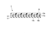
- FIG. 1 is a cross-sectional view schematically showing an embodiment of the support sheet of the present invention.
- the support sheet 1 shown here includes an adhesive layer 12 on a base material 11, and further includes a release film 15 on the adhesive layer 12.
- a pressure-sensitive adhesive layer 12 is laminated on one surface (first surface) 11a of the base material 11, and the other surface of the base material 11, that is, the side opposite to the side having the pressure-sensitive adhesive layer 12 is provided.
- the surface (second surface) 11b is an exposed surface.
- the first surface 11 a has a surface roughness of 0.4 ⁇ m or less
- the second surface 11 b has a surface roughness larger than the surface roughness of the first surface 11 a and 0.053. 0.48 ⁇ m.
- surface roughness means a so-called arithmetic average roughness obtained in accordance with JIS B0601: 2001, and is abbreviated as “Ra” unless otherwise specified.
- the release film 15 is here.
- first surface 12 a On one surface of the pressure-sensitive adhesive layer 12, that is, on the surface opposite to the side on which the substrate 11 is provided (hereinafter sometimes referred to as “first surface”) 12 a, the release film 15 is here.
- symbol 12b means the other surface of the adhesive layer 12, ie, the surface (the following may be called "the 2nd surface") by which the base material 11 is provided.
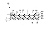
- FIG. 2 is a cross-sectional view schematically showing one embodiment of the composite sheet for forming a protective film of the present invention.
- the protective film-forming composite sheet 101 shown here includes an adhesive layer 12 on a base material 11 and a protective film-forming film 13 on the adhesive layer 12.
- the protective sheet-forming composite sheet 101 can be configured using the support sheet 1, and it can be said that the protective film-forming film 13 is further provided on the pressure-sensitive adhesive layer 12 in the support sheet 1.
- the protective film forming film 13 is laminated on the entire first surface 12 a of the pressure-sensitive adhesive layer 12.
- first surface 13a a part of the surface 13a opposite to the side on which the pressure-sensitive adhesive layer 12 of the protective film-forming film 13 is provided (hereinafter sometimes referred to as “first surface”) 13a, that is, in the vicinity of the periphery In the region, a jig adhesive layer 14 is laminated.
- first surface 13 a of the protective film forming film 13 the surface on which the jig adhesive layer 14 is not laminated is not in contact with the protective film forming film 13 of the jig adhesive layer 14.
- a release film 15 is laminated on the surface (first surface 14a and side surface 14c).
- the first surface 14a of the jig adhesive layer 14 is a surface opposite to the side of the jig adhesive layer 14 that is in contact with the protective film forming film 13, and is used for the jig. In some cases, the boundary between the first surface 14a and the side surface 14c of the adhesive layer 14 cannot be clearly distinguished. Further, the release film 15 may not be in contact with the side surface 14c of the jig adhesive layer 14.
- the protective sheet-forming composite sheet 1 is usually stored in a state in which the release film 15 is provided as described above.
- reference numeral 15 a indicates the surface of the release film 15 opposite to the side in contact with the protective film-forming film 13 (hereinafter sometimes referred to as “first surface”). .
- the protective film-forming composite sheet 101 is a surface on which a circuit of a semiconductor wafer (not shown) is formed by the first surface 13a of the protective film-forming film 13 with the release film 15 removed (this specification). Is affixed to a surface opposite to the “circuit forming surface” (which may be abbreviated as “back surface” in this specification), and The first surface 14a is used by being attached to a jig such as a ring frame.
- the second surface 11b of the substrate 11 has a surface roughness of 0.053 to 0.48 ⁇ m, and this surface roughness is equal to that of the first surface 11a of the substrate 11. It is larger than the surface roughness and has an appropriate uneven shape.
- the protective film forming film 13 is applied to the surface (back surface) opposite to the circuit forming surface of the semiconductor wafer or semiconductor chip, it is made into a protective film by curing.
- Printing may be performed by irradiation of laser light from the second surface 11b side of the substrate 11. At this time, the laser light enters the support sheet 1 from the second surface 11b side of the substrate 11 and reaches the protective film. Therefore, as described above, the second surface 11b of the substrate 11 has an appropriate uneven shape, and the irregularity is low, so that the irregular reflection of the laser light on the second surface 11b of the substrate 11 is suppressed, and the protective film is formed. Clear laser printing is possible.
- the protective film forming composite sheet 101 or the semiconductor wafer or semiconductor chip provided with the protective film is inspected by an infrared camera or the like through the protective film forming composite sheet 101 or the protective film.
- the second surface 11b of the base material 11 has an appropriate uneven shape, and the irregularity is low, so that irregular reflection of infrared rays on the second surface 11b of the base material 11 is suppressed, and a clear inspection is performed. Images can be acquired.
- the pressure-sensitive adhesive is used to reduce the influence of the uneven surface on the pressure-sensitive adhesive layer.
- the layer should be soft and thick enough. This is because when the pressure-sensitive adhesive layer is hard, the pressure-sensitive adhesive layer may not be filled in the vicinity of the base of the convex portion on the surface of the base material, and a void may be formed. This is because the surface (back surface) on the substrate side of the protective film-forming film becomes an uneven surface reflecting the uneven shape on the surface.
- the first surface 11a of the substrate 11 on which the pressure-sensitive adhesive layer 12 is provided has a surface roughness of 0.4 ⁇ m or less and high smoothness ( Since the unevenness is low), the above-described problems can be avoided. That is, in the protective film-forming composite sheet 101, the first surface 11a of the substrate 11 can be sufficiently embedded with the pressure-sensitive adhesive layer 12, and it is not necessary to form the pressure-sensitive adhesive layer 12 thick. Can be suppressed.
- FIG. 3 is a cross-sectional view schematically showing another embodiment of the composite sheet for forming a protective film of the present invention.
- the protective film-forming composite sheet 102 shown here is the same as the protective film-forming composite sheet 101 shown in FIG. 2 except that the shape of the protective film-forming film is different and the jig adhesive layer is not provided. It is. That is, the protective film-forming composite sheet 102 includes the adhesive layer 12 on the base material 11, the protective film-forming film 23 on the adhesive layer 12, and the protective film-forming film 23 on the protective film-forming film 23. A release film 15 is provided.
- the protective film-forming film 23 is laminated on a part of the first surface 12 a of the pressure-sensitive adhesive layer 12, that is, a region on the center side in the width direction (left-right direction in FIG. 3) of the support sheet 1.
- the first surface 12 a of the pressure-sensitive adhesive layer 12 the surface on which the protective film-forming film 23 is not laminated and the surface of the protective film-forming film 23 that is not in contact with the pressure-sensitive adhesive layer 12 (first surface 23 a Further, the release film 15 is laminated on the side surface 23c).
- the first surface 23a of the protective film-forming film 23 is a surface opposite to the side in contact with the pressure-sensitive adhesive layer 12 of the protective film-forming film 23.
- the boundary between the first surface 23a and the side surface 23c cannot be clearly distinguished. Further, the release film 15 may not be in contact with the side surface 23 c of the protective film forming film 23.
- the composite sheet 102 for forming a protective film is usually stored with the release film 15 as described above.
- the protective film-forming composite sheet 102 is attached to the back surface of the semiconductor wafer (not shown) by the first surface 23a of the protective film-forming film 23 with the release film 15 removed, and further, the adhesive layer 12 Of the first surface 12a, the surface on which the protective film forming film 23 is not laminated is attached to a jig such as a ring frame and used.
- the protective sheet-forming composite sheet 102 also has a surface roughness of the first surface 11a of the substrate 11 of 0.4 ⁇ m or less, and the surface roughness of the second surface 11b is larger than the surface roughness of the first surface 11a. And 0.053 to 0.48 ⁇ m.
- the protective film-forming composite sheet 102 as in the case of the protective film-forming composite sheet 101, is insufficiently embedded in the first surface 11a of the base material 11 by the adhesive layer 12, and It is possible to suppress blocking, obtain clear laser printing on a protective film, and obtain a clear inspection image of a semiconductor wafer or semiconductor chip without causing any defects.
- FIG. 4 is a cross-sectional view schematically showing still another embodiment of the composite sheet for forming a protective film of the present invention.
- the protective film-forming composite sheet 103 shown here is further provided for the jig on the surface of the first surface 12a of the pressure-sensitive adhesive layer 12 where the protective film-forming film 23 is not laminated, that is, in the vicinity of the peripheral edge. Except that the adhesive layer 14 is laminated, it is the same as the composite sheet 102 for forming a protective film shown in FIG.
- the protective film-forming composite sheet 103 is attached to the back surface of the semiconductor wafer (not shown) by the first surface 23a of the protective film-forming film 23 in a state where the release film 15 is removed.
- the first surface 14a of the agent layer 14 is used by being attached to a jig such as a ring frame.
- the protective sheet-forming composite sheet 103 also has a surface roughness of the first surface 11a of the substrate 11 of 0.4 ⁇ m or less, and the surface roughness of the second surface 11b is larger than the surface roughness of the first surface 11a. And 0.053 to 0.48 ⁇ m.
- the protective film-forming composite sheet 103 is not sufficiently embedded in the first surface 11a of the base material 11 by the pressure-sensitive adhesive layer 12, as in the case of the protective film-forming composite sheet 101. It is possible to suppress blocking, obtain clear laser printing on a protective film, and obtain a clear inspection image of a semiconductor wafer or semiconductor chip without causing any defects.
- the composite sheet for forming a protective film of the present invention is not limited to the one shown in FIGS. 2 to 4, and a part of the structure shown in FIGS. In addition, another configuration may be added to what has been described so far. Next, the structure of each layer of the support sheet and the composite sheet for forming a protective film of the present invention will be described.
- the surface roughness of the base material on the side (first surface) provided with the pressure-sensitive adhesive layer is 0.4 ⁇ m or less, for example, 0.37 ⁇ m or less, 0.3 ⁇ m or less, 0 .2 ⁇ m or less, 0.1 ⁇ m or less, 0.09 ⁇ m or less, 0.08 ⁇ m or less, 0.07 ⁇ m or less, or 0.06 ⁇ m or less, etc., but these are only examples.
- the lower limit value of the surface roughness on the first surface of the substrate is not particularly limited, and may be 0.01 ⁇ m, for example, but this is an example.
- Preferred examples of the surface roughness on the first surface include 0.01 to 0.4 ⁇ m, 0.01 to 0.37 ⁇ m, 0.01 to 0.3 ⁇ m, 0.01 to 0.2 ⁇ m, and 0.01 to Examples thereof include 0.1 ⁇ m, 0.01 to 0.09 ⁇ m, 0.01 to 0.08 ⁇ m, 0.01 to 0.07 ⁇ m, and 0.01 to 0.06 ⁇ m.
- the surface roughness of the surface (second surface) on the side opposite to the side having the pressure-sensitive adhesive layer of the substrate is 0.053 to 0.48 ⁇ m. 055 ⁇ m or more, 0.08 ⁇ m or more, 0.15 ⁇ m or more, 0.25 ⁇ m or more, 0.35 ⁇ m or more, etc., and 0.47 ⁇ m or less, 0.45 ⁇ m or less, 0.35 ⁇ m or less, 0.25 ⁇ m or less
- Preferred examples of the surface roughness on the second surface include 0.053 to 0.47 ⁇ m, 0.053 to 0.45 ⁇ m, 0.053 to 0.35 ⁇ m, 0.053 to 0.25 ⁇ m, and 0.053. Up to 0.15 ⁇ m.
- the surface roughness on the second surface include 0.055 to 0.48 ⁇ m, 0.08 to 0.48 ⁇ m, 0.15 to 0.48 ⁇ m, 0.25 to 0.48 ⁇ m, and 0 .35 to 0.48 ⁇ m. However, the surface roughness on the second surface is larger than the surface roughness on the first surface.
- the base material is, for example, a method of forming a smooth surface and an uneven surface at the same time using a raw material (hereinafter sometimes abbreviated as “raw material base material”), or a smooth surface and an uneven surface separately. It can produce by the method of forming in this.
- a raw material base material is sandwiched between a pair of rolls having different smoothnesses on the roll surface, and the roll surface is rotated while rotating these rolls.
- a smooth surface is formed from the roll surface having a high smoothness (smooth surface of the roll) and a rough surface from the roll surface having a low smoothness (uneven surface of the roll).
- a method of forming a base material for example, a raw material base material is sandwiched between a pair of rolls having different smoothnesses on the roll surface, and the roll surface is rotated while rotating these rolls.
- a smooth surface is formed from the roll surface having a high smoothness (smooth surface of the roll) and a rough surface from the roll surface having a low smoothness (uneven surface of the roll).
- a method for producing a substrate on which a smooth surface and an uneven surface are separately formed for example, a raw material substrate having a surface roughness of 0.4 ⁇ m or less on one or both sides is used, and finally a smooth surface (surface roughness) A surface having a surface roughness of 0.4 ⁇ m or less, and the other surface different from this is an uneven surface having a surface roughness larger than that of the smooth surface (surface roughness is 0.053 to 0).
- a method of producing a base material by performing a smoothing treatment or a roughening treatment so that the surface is .48 ⁇ m) can be mentioned.
- an embossing method which presses a raw material base material to the smooth surface or uneven
- a smooth surface or an uneven surface is formed on the raw material base material by transferring a shape such as a roll surface, the smoothness on the smooth surface such as the roll surface, or the unevenness on the uneven surface.
- the surface roughness of the substrate can be adjusted.
- a smoothing process or a roughening process is performed on one surface of the raw material base material which is finally a smooth surface (surface having a surface roughness of 0.4 ⁇ m or less). The surface roughness may be adjusted within a range of 0.4 ⁇ m or less.
- the method for setting the surface roughness of one surface of the substrate to 0.053 to 0.48 ⁇ m using the smooth surface or the uneven surface of the roll has been described.
- mold used for is not limited to a roll, The thing of other shapes, such as a plate and a block, may be sufficient.
- embossing method for example, a sand blasting method, a solvent processing method, and the like can be used as the method for forming the surface roughness of the raw material base material.
- a method for producing a base material having a surface roughness of both surfaces satisfying the above-described conditions using a raw material base material having a surface roughness of 0.4 ⁇ m or less on one side or both sides has been described.
- the other surface different from this is subjected to a smoothing treatment or a roughening treatment so that the surface becomes a smooth surface having a surface roughness smaller than that of the concave-convex surface (a surface having a surface roughness of 0.4 ⁇ m or less).
- a smoothing treatment or a roughening treatment so that the surface becomes a smooth surface having a surface roughness smaller than that of the concave-convex surface (a surface having a surface roughness of 0.4 ⁇ m or less).
- the method of producing a base material is also mentioned. In this method, if necessary, the surface of one surface of the raw material base material that is the uneven surface (surface having a surface roughness of 0.053 to 0.48 ⁇ m) is smoothed or uneven. The surface roughness may be adjusted within the range of 0.053 to 0.48 ⁇ m.
- a method for producing the base material a method of simultaneously forming a smooth surface and an uneven surface using a raw material base material is preferable.
- the constituent material of the base material is preferably various resins, and the resin may be a known one. However, it is preferable that the base material has both light transmittance with a wavelength of 532 nm and light with a wavelength of 1600 nm. Light having a wavelength of 532 nm is suitable for performing laser printing of a protective film, and light having a wavelength of 1600 nm is suitable for performing infrared inspection of a semiconductor wafer or semiconductor chip. Furthermore, when the adhesive layer described later is energy ray curable, the substrate preferably has light permeability in the ultraviolet region. Specific constituent materials of the substrate will be described later.
- the tensile elastic modulus of the substrate is not particularly limited, but is preferably 240 to 700 MPa, more preferably 280 to 650 MPa, and particularly preferably 320 to 600 MPa.
- the substrate may be composed of one layer (single layer) or may be composed of two or more layers.
- a base material consists of multiple layers, these multiple layers may be the same as or different from each other. That is, all the layers may be the same, all the layers may be different, or only some of the layers may be the same. And when several layers differ from each other, the combination of these several layers is not specifically limited.
- the phrase “the plurality of layers are different from each other” means that not only the substrate but also at least one of the constituent materials and thicknesses of the respective layers is different from each other.
- the thickness of the substrate can be appropriately selected according to the purpose, but is preferably 15 to 300 ⁇ m, more preferably 20 to 200 ⁇ m, for example, any of 30 to 160 ⁇ m, 40 to 120 ⁇ m, and the like. It may be. When the thickness of the substrate is within such a range, the flexibility of the composite sheet for forming a protective film and the adhesiveness to a semiconductor wafer or semiconductor chip are further improved.
- the thickness of the substrate means the thickness of the entire substrate.
- the thickness of the substrate composed of a plurality of layers means the total thickness of all the layers constituting the substrate.
- At least one surface of the base material is a non-smooth surface having a surface roughness of 0.053 ⁇ m or more and an uneven shape. If the tip of the part is taken as one starting point, it can be calculated with higher accuracy.
- the pressure-sensitive adhesive layer may be either energy ray curable or non-energy ray curable.
- energy beam curability means a property of being cured by irradiation with energy rays. On the contrary, the property that does not cure even when irradiated with energy rays is referred to as “non-energy ray curable”.
- energy beam means an electromagnetic wave or a charged particle beam having energy quanta, and examples thereof include ultraviolet rays, radiation, and electron beams.
- Ultraviolet rays can be irradiated by using, for example, a high-pressure mercury lamp, a fusion H lamp, a xenon lamp, a black light, an LED lamp or the like as an ultraviolet ray source.
- the electron beam can be emitted by an electron beam accelerator or the like.
- the constituent material of the pressure-sensitive adhesive layer examples include a pressure-sensitive adhesive such as a pressure-sensitive resin, and a crosslinking agent.
- the pressure-sensitive adhesive layer has both light transmittance with a wavelength of 532 nm and light with a wavelength of 1600 nm. Light having a wavelength of 532 nm is suitable for performing laser printing of a protective film, and light having a wavelength of 1600 nm is suitable for performing infrared inspection of a semiconductor wafer or semiconductor chip.
- the storage elastic modulus of the pressure-sensitive adhesive layer is not particularly limited, but is usually preferably 0.01 to 1000 MPa, more preferably 0.01 to 500 MPa, and particularly preferably 0.01 to 300 MPa. preferable.
- the storage elastic modulus of the pressure-sensitive adhesive layer can be adjusted by adjusting the type or amount of the components contained in the pressure-sensitive adhesive layer.
- the “storage elastic modulus of the pressure-sensitive adhesive layer” means “the storage elastic modulus of the pressure-sensitive adhesive layer before curing” when the pressure-sensitive adhesive layer is curable, unless otherwise specified. means.
- the storage elastic modulus of the pressure-sensitive adhesive layer is determined by the following method. That is, the pressure-sensitive adhesive layers are bonded to each other to produce a pressure-sensitive adhesive layer laminate having a thickness of 800 ⁇ m, and the laminate is punched into a circle having a diameter of 10 mm to form a test piece. The test piece is strained at a frequency of 1 Hz, the storage elastic modulus at ⁇ 50 to 150 ° C. is measured, and the value of the storage elastic modulus at 23 ° C. is taken as the storage elastic modulus of the pressure-sensitive adhesive layer.
- the thickness of the pressure-sensitive adhesive layer can be appropriately selected depending on the purpose, but is preferably 1 to 50 ⁇ m, more preferably 1 to 40 ⁇ m, and particularly preferably 1 to 30 ⁇ m.
- the adhesive force with respect to the film for protective film formation of an adhesive layer improves more because the thickness of an adhesive layer is more than the said lower limit. Furthermore, the effect of embedding the uneven shape on the first surface of the base material becomes higher, and the influence of the pressure-sensitive adhesive layer on the uneven shape can be further reduced. On the other hand, when the thickness of the pressure-sensitive adhesive layer is not more than the above upper limit value, the effect of suppressing chipping is further increased, and the dicing process is further stabilized.
- the “thickness of the pressure-sensitive adhesive layer” means the thickness of the whole pressure-sensitive adhesive layer.
- the thickness of the pressure-sensitive adhesive layer composed of a plurality of layers is the total of all layers constituting the pressure-sensitive adhesive layer. Means the thickness.
- the surface roughness of the first surface of the base material is 0.4 ⁇ m or less, and the surface on the side where the base material of the pressure-sensitive adhesive layer is provided in accordance with such an uneven shape.
- the (second surface) may be a non-smooth surface having an uneven shape with a surface roughness of 0.1 ⁇ m or more. In that case, the thickness of the pressure-sensitive adhesive layer can be calculated with higher accuracy in a region including the convex portion of the pressure-sensitive adhesive layer if the tip of the convex portion is set as one starting point.
- the hardness of the pressure-sensitive adhesive layer it is preferable to adjust the hardness of the pressure-sensitive adhesive layer according to its thickness.
- the above-mentioned storage elastic modulus is mentioned, for example.
- the thickness of the pressure-sensitive adhesive layer is preferably more than 15 ⁇ m (thicker than 15 ⁇ m), more preferably 18 ⁇ m or more
- the storage elastic modulus of the pressure-sensitive adhesive layer is 30 kPa or more. Is more preferable, 40 kPa or more is more preferable, and 50 kPa or more is particularly preferable.
- the upper limit value of the storage elastic modulus of the pressure-sensitive adhesive layer can be set to, for example, the upper limit value of the normal values listed above.
- semiconductor chips and semiconductor wafers that are being cut in the process of becoming semiconductor chips are also less likely to vibrate, and an extra force is applied to these semiconductor chips and semiconductor wafers, resulting in so-called cracking and chipping of the semiconductor chips. Chipping is suppressed.
- the storage elastic modulus of the pressure-sensitive adhesive layer is not particularly limited.
- the storage elastic modulus of the pressure-sensitive adhesive layer can be set, for example, to the normal range mentioned above, but this is an example.
- the storage elastic modulus of the pressure-sensitive adhesive layer is also preferably set in the same range as in the case where the pressure-sensitive adhesive layer is thick.
- the pressure-sensitive adhesive layer can be formed using a pressure-sensitive adhesive composition containing a pressure-sensitive adhesive.
- an adhesive layer can be formed in the target site
- a more specific method for forming the pressure-sensitive adhesive layer will be described later in detail, along with methods for forming other layers.
- the ratio of the content of components that do not vaporize at room temperature in the pressure-sensitive adhesive composition is usually the same as the ratio of the content of the components of the pressure-sensitive adhesive layer.
- “normal temperature” means a temperature that is not particularly cooled or heated, that is, a normal temperature, and examples thereof include a temperature of 15 to 25 ° C.
- the said adhesive composition is obtained by mix
- the order of addition at the time of blending each component is not particularly limited, and two or more components may be added simultaneously.
- the method of mixing each component at the time of compounding is not particularly limited, from a known method such as a method of mixing by rotating a stirrer or a stirring blade; a method of mixing using a mixer; a method of mixing by applying ultrasonic waves What is necessary is just to select suitably.
- the temperature and time during the addition and mixing of each component are not particularly limited as long as each compounding component does not deteriorate, and may be adjusted as appropriate, but the temperature is preferably 15 to 30 ° C.
- the adhesive composition may be applied by a known method, for example, an air knife coater, blade coater, bar coater, gravure coater, roll coater, roll knife coater, curtain coater, die coater, knife coater, screen coater. And a method using various coaters such as a Meyer bar coater and a kiss coater.
- drying conditions of an adhesive composition are not specifically limited, When the adhesive composition contains the solvent mentioned later, it is preferable to heat-dry.
- the pressure-sensitive adhesive composition containing the solvent is preferably dried, for example, at 70 to 130 ° C. for 10 seconds to 5 minutes.
- a support sheet provided with the base material and adhesive layer which consist of the above-mentioned constituent materials for example, it is described in patent 4805549, and consists of a base film and an adhesive layer formed thereon.
- a pressure-sensitive adhesive sheet, a pressure-sensitive adhesive sheet described in Japanese Patent No. 4781633, a base film and a pressure-sensitive adhesive layer formed thereon, and a base material described in Japanese Patent No. 5414953, and at least one of them A dicing sheet having a pressure-sensitive adhesive layer laminated on the surface, and described in JP 2013-199562 A for processing a workpiece having a pressure-sensitive adhesive resin layer (pressure-sensitive adhesive layer) on at least one side of a substrate A sheet etc. are mentioned.
- the support sheet of the present invention those having the same constituent materials as those of the sheet and having the surface roughness of the first surface and the second surface adjusted to the above numerical range are preferable.
- the protective film-forming film has curability and forms a protective film by curing.
- the protective film-forming film may be either thermosetting or energy ray curable.
- thermosetting protective film examples include those containing a polymer component (A) and a thermosetting component (B).
- the polymer component (A) is a component that can be regarded as formed by polymerization reaction of the polymerizable compound.
- the thermosetting component (B) is a component that can undergo a curing (polymerization) reaction using heat as a reaction trigger.
- the polymerization reaction includes a polycondensation reaction.
- thermosetting protective film-forming film may be composed of one layer (single layer), or may be composed of two or more layers.
- the thermosetting protective film-forming film is composed of a plurality of layers, the plurality of layers may be the same as or different from each other.
- “the plurality of layers may be the same as or different from each other” means the same as in the case of the above-described base material. And when several layers differ from each other, the combination of these several layers is not specifically limited.
- the thickness of the thermosetting protective film-forming film is preferably 1 to 100 ⁇ m, more preferably 5 to 75 ⁇ m, and particularly preferably 5 to 50 ⁇ m.
- a protective film with higher protective ability can be formed.
- an excessive thickness is suppressed.
- the “thickness of the thermosetting protective film forming film” means the thickness of the entire thermosetting protective film forming film, for example, a thermosetting protective film forming film composed of a plurality of layers. The thickness means the total thickness of all the layers constituting the thermosetting protective film forming film.
- thermosetting protective film-forming film when the thermosetting protective film-forming film is applied to the back surface of the semiconductor wafer and cured to form the protective film are particularly set as long as the degree of curing is such that the protective film exhibits its function sufficiently. It is not limited, What is necessary is just to select suitably according to the kind of film for thermosetting protective film formation.
- the heating temperature during curing of the thermosetting protective film-forming film is preferably 100 to 200 ° C., more preferably 110 to 180 ° C., and particularly preferably 120 to 170 ° C.
- the heating time at the time of curing is preferably 0.5 to 5 hours, more preferably 0.5 to 3 hours, and particularly preferably 1 to 2 hours.
- the composition for forming a thermosetting protective film can be formed using a composition for forming a thermosetting protective film containing the constituent materials.
- the composition for forming a thermosetting protective film is applied to the surface to be formed of the film for forming a thermosetting protective film, and dried as necessary to form a thermosetting protective film on the target site.
- a film can be formed.
- the ratio of the content of components that do not vaporize at room temperature in the thermosetting protective film-forming composition is usually the same as the content ratio of the components of the thermosetting protective film-forming film.
- “normal temperature” is as described above.
- thermosetting protective film forming composition The drying conditions of the thermosetting protective film forming composition are not particularly limited, but the thermosetting protective film forming composition is preferably dried by heating when it contains a solvent described later.
- the composition for forming a thermosetting protective film containing a solvent is preferably dried at 70 to 130 ° C. for 10 seconds to 5 minutes, for example.
- composition (III-1) a composition (III-1) for forming a thermosetting protective film containing a polymer component (A) and a thermosetting component (B) (in this specification) May be simply abbreviated as “composition (III-1)”).
- the polymer component (A) is a polymer compound for imparting film-forming properties, flexibility and the like to the thermosetting protective film-forming film.
- the polymer component (A) contained in the composition (III-1) and the thermosetting protective film-forming film may be only one kind, two kinds or more, and combinations of two or more kinds. The ratio can be arbitrarily selected.
- Examples of the polymer component (A) include an acrylic resin (a resin having a (meth) acryloyl group), a polyester, a urethane resin (a resin having a urethane bond), an acrylic urethane resin, and a silicone resin (having a siloxane bond). Resin), rubber resin (resin having a rubber structure), phenoxy resin, thermosetting polyimide and the like, and acrylic resin is preferable.
- (meth) acryloyl group is a concept including both “acryloyl group” and “methacryloyl group”.
- (meth) acrylic acid is a concept including both “acrylic acid” and “methacrylic acid”
- (meth) acrylate” Is a concept including both” acrylate "and” methacrylate ".
- the weight average molecular weight (Mw) of the acrylic resin is preferably 10,000 to 2,000,000, and more preferably 100,000 to 1500,000.
- Mw weight average molecular weight
- the weight average molecular weight of the acrylic resin is equal to or more than the lower limit, the shape stability (time stability during storage) of the thermosetting protective film-forming film is improved.
- the weight average molecular weight of the acrylic resin is not more than the above upper limit value, the thermosetting protective film forming film easily follows the uneven surface of the adherend, and the adherend and the thermosetting protective film are formed. Occurrence of voids and the like with the film is further suppressed.
- the weight average molecular weight is a polystyrene conversion value measured by a gel permeation chromatography (GPC) method unless otherwise specified.
- the acrylic resin is selected from, for example, a polymer of one or more (meth) acrylic acid esters; (meth) acrylic acid, itaconic acid, vinyl acetate, acrylonitrile, styrene, N-methylolacrylamide, and the like. Examples include copolymers of two or more monomers.
- Examples of the (meth) acrylic acid ester constituting the acrylic resin include methyl (meth) acrylate, ethyl (meth) acrylate, n-propyl (meth) acrylate, isopropyl (meth) acrylate, (meth ) N-butyl acrylate, isobutyl (meth) acrylate, sec-butyl (meth) acrylate, tert-butyl (meth) acrylate, pentyl (meth) acrylate, hexyl (meth) acrylate, (meth) acrylic Heptyl acid, 2-ethylhexyl (meth) acrylate, isooctyl (meth) acrylate, n-octyl (meth) acrylate, n-nonyl (meth) acrylate, isononyl (meth) acrylate, decyl (meth) acrylate , Undecyl (me
- the acrylic resin is, for example, one or more monomers selected from (meth) acrylic acid, itaconic acid, vinyl acetate, acrylonitrile, styrene, N-methylolacrylamide and the like in addition to the (meth) acrylic ester. May be obtained by copolymerization.
- Only one type of monomer constituting the acrylic resin may be used, or two or more types may be used, and in the case of two or more types, the combination and ratio thereof can be arbitrarily selected.
- the acrylic resin may have a functional group that can be bonded to other compounds such as a vinyl group, a (meth) acryloyl group, an amino group, a hydroxyl group, a carboxy group, and an isocyanate group.
- the functional group of the acrylic resin may be bonded to another compound via a cross-linking agent (F) described later, or may be directly bonded to another compound not via the cross-linking agent (F). .
- F cross-linking agent
- thermoplastic resin other than an acrylic resin
- thermoplastic resin is used alone without using an acrylic resin.
- it may be used in combination with an acrylic resin.
- the weight average molecular weight of the thermoplastic resin is preferably 1000 to 100,000, more preferably 3000 to 80,000.
- the glass transition temperature (Tg) of the thermoplastic resin is preferably ⁇ 30 to 150 ° C., and more preferably ⁇ 20 to 120 ° C.
- thermoplastic resin examples include polyester, polyurethane, phenoxy resin, polybutene, polybutadiene, and polystyrene.
- thermoplastic resin contained in the composition (III-1) and the thermosetting protective film-forming film may be only one kind, two kinds or more, and in the case of two kinds or more, combinations and ratios thereof. Can be chosen arbitrarily.
- the ratio of the content of the polymer component (A) to the total content of all components other than the solvent (that is, the polymer component (A) of the thermosetting protective film-forming film) is preferably 5 to 85% by mass, more preferably 5 to 80% by mass, regardless of the type of the polymer component (A), for example, 10 to 70% by mass, 20 to The amount may be 60% by mass or 30 to 50% by mass.
- the polymer component (A) may also correspond to the thermosetting component (B).
- the composition (III-1) contains components corresponding to both the polymer component (A) and the thermosetting component (B), the composition (III-1) The polymer component (A) and the thermosetting component (B) are considered to be contained.
- thermosetting component (B) is a component for curing a thermosetting protective film-forming film to form a hard protective film.
- the thermosetting component (B) contained in the composition (III-1) and the thermosetting protective film-forming film may be only one type, two or more types, and when two or more types, Combinations and ratios can be arbitrarily selected.
- thermosetting component (B) examples include epoxy thermosetting resins, thermosetting polyimides, polyurethanes, unsaturated polyesters, and silicone resins, and epoxy thermosetting resins are preferable.
- the epoxy thermosetting resin includes an epoxy resin (B1) and a thermosetting agent (B2).
- the epoxy thermosetting resin contained in the composition (III-1) and the thermosetting protective film-forming film may be only one type, two or more types, and combinations of two or more types. The ratio can be arbitrarily selected.
- Epoxy resin (B1) examples include known ones such as polyfunctional epoxy resins, biphenyl compounds, bisphenol A diglycidyl ether and hydrogenated products thereof, orthocresol novolac epoxy resins, dicyclopentadiene type epoxy resins, Biphenyl type epoxy resins, bisphenol A type epoxy resins, bisphenol F type epoxy resins, phenylene skeleton type epoxy resins, and the like, and bifunctional or higher functional epoxy compounds are listed.
- an epoxy resin having an unsaturated hydrocarbon group may be used as the epoxy resin (B1).
- An epoxy resin having an unsaturated hydrocarbon group is more compatible with an acrylic resin than an epoxy resin having no unsaturated hydrocarbon group. Therefore, by using an epoxy resin having an unsaturated hydrocarbon group, the reliability of the semiconductor chip with a protective film obtained using the composite sheet for forming a protective film is improved.
- Examples of the epoxy resin having an unsaturated hydrocarbon group include compounds obtained by converting a part of the epoxy group of a polyfunctional epoxy resin into a group having an unsaturated hydrocarbon group. Such a compound can be obtained, for example, by addition reaction of (meth) acrylic acid or a derivative thereof to an epoxy group. Moreover, as an epoxy resin which has an unsaturated hydrocarbon group, the compound etc. which the group which has an unsaturated hydrocarbon group directly couple
- the unsaturated hydrocarbon group is a polymerizable unsaturated group, and specific examples thereof include ethenyl group (vinyl group), 2-propenyl group (allyl group), (meth) acryloyl group, (meth) An acrylamide group etc. are mentioned, An acryloyl group is preferable.
- the number average molecular weight of the epoxy resin (B1) is not particularly limited, but is 300 to 30000 from the viewpoint of the curability of the thermosetting protective film-forming film and the strength and heat resistance of the cured protective film. Preferably, it is 300 to 10,000, more preferably 300 to 3000.
- the epoxy equivalent of the epoxy resin (B1) is preferably 100 to 1000 g / eq, and more preferably 150 to 950 g / eq.
- the epoxy resin (B1) may be used alone or in combination of two or more, and when two or more are used in combination, their combination and ratio can be arbitrarily selected.
- thermosetting agent (B2) functions as a curing agent for the epoxy resin (B1).
- a thermosetting agent (B2) the compound which has 2 or more of functional groups which can react with an epoxy group in 1 molecule is mentioned, for example.
- the functional group include a phenolic hydroxyl group, an alcoholic hydroxyl group, an amino group, a carboxy group, a group in which an acid group has been anhydrideized, and the like, and a phenolic hydroxyl group, an amino group, or an acid group has been anhydrideized. It is preferably a group, more preferably a phenolic hydroxyl group or an amino group.
- thermosetting agents (B2) examples of the phenolic curing agent having a phenolic hydroxyl group include polyfunctional phenol resins, biphenols, novolac type phenol resins, dicyclopentadiene type phenol resins, and aralkyl type phenol resins. .
- examples of the amine-based curing agent having an amino group include dicyandiamide (hereinafter sometimes abbreviated as “DICY”).
- the thermosetting agent (B2) may have an unsaturated hydrocarbon group.
- examples of the thermosetting agent (B2) having an unsaturated hydrocarbon group include compounds in which a part of the hydroxyl group of the phenol resin is substituted with a group having an unsaturated hydrocarbon group, and the aromatic ring of the phenol resin. Examples thereof include compounds in which a group having a saturated hydrocarbon group is directly bonded.
- the unsaturated hydrocarbon group in the thermosetting agent (B2) is the same as the unsaturated hydrocarbon group in the epoxy resin having the unsaturated hydrocarbon group described above.
- thermosetting agent (B2) When using a phenolic curing agent as the thermosetting agent (B2), it is preferable that the thermosetting agent (B2) has a high softening point or glass transition temperature in terms of improving the peelability of the protective film from the support sheet. .
- thermosetting agent (B2) for example, the number average molecular weight of the resin component such as polyfunctional phenol resin, novolac type phenol resin, dicyclopentadiene type phenol resin, aralkyl type phenol resin is preferably 300 to 30,000. 400 to 10,000 is more preferable, and 500 to 3000 is particularly preferable.
- the molecular weight of non-resin components such as biphenol and dicyandiamide is not particularly limited, but is preferably 60 to 500, for example.
- thermosetting agent (B2) may be used individually by 1 type, may use 2 or more types together, and when using 2 or more types together, those combinations and ratios can be selected arbitrarily.
- the content of the thermosetting agent (B2) is 0.1 to 500 masses with respect to 100 mass parts of the epoxy resin (B1) content. Parts, preferably 1 to 200 parts by weight, for example, 1 to 100 parts by weight, 1 to 50 parts by weight, and 1 to 25 parts by weight.
- the content of the thermosetting agent (B2) is equal to or higher than the lower limit value, the curing of the thermosetting protective film forming film more easily proceeds.
- the moisture absorption rate of the film for thermosetting protective film formation was reduced because the said content of the thermosetting agent (B2) was below the said upper limit, and it was obtained using the composite sheet for protective film formation Improved package reliability.
- the content of the thermosetting component (B) (for example, the total content of the epoxy resin (B1) and the thermosetting agent (B2)) is:
- the content of the polymer component (A) is preferably 20 to 500 parts by mass, more preferably 30 to 300 parts by mass, and particularly preferably 40 to 150 parts by mass with respect to 100 parts by mass of the polymer component (A).
- it may be any of 40 to 125 parts by mass, 40 to 100 parts by mass, and 40 to 75 parts by mass.
- the curing accelerator (C) contained in the composition (III-1) and the film for forming a thermosetting protective film may be only one type, two or more types, or a combination of two or more types.
- the ratio can be arbitrarily selected.
- the filler (D) may be either an organic filler or an inorganic filler, but is preferably an inorganic filler.
- Preferred inorganic fillers include, for example, powders of silica, alumina, talc, calcium carbonate, titanium white, bengara, silicon carbide, boron nitride, and the like; beads formed by spheroidizing these inorganic fillers; surface modification of these inorganic fillers Products; single crystal fibers of these inorganic fillers; glass fibers and the like.
- the inorganic filler is preferably silica or alumina.
- the filler (D) contained in the composition (III-1) and the thermosetting protective film-forming film may be only one type, two or more types, and when two or more types are combined, The ratio can be arbitrarily selected.
- the ratio of the content of the filler (D) to the total content of all components other than the solvent in the composition (III-1) that is, a film for forming a thermosetting protective film
- the content of the filler (D) is preferably 5 to 80% by mass, more preferably 7 to 60% by mass, such as 10 to 50% by mass, 15 to 45% by mass, and It may be any one of 20 to 40% by mass. Adjustment of said thermal expansion coefficient becomes easier because content of a filler (D) is such a range.
- the coupling agent (E) is preferably a compound having a functional group capable of reacting with the functional group of the polymer component (A), the thermosetting component (B), etc., and is preferably a silane coupling agent. More preferred. Preferred examples of the silane coupling agent include 3-glycidyloxypropyltrimethoxysilane, 3-glycidyloxypropylmethyldiethoxysilane, 3-glycidyloxypropyltriethoxysilane, 3-glycidyloxymethyldiethoxysilane, 2- (3,4-epoxycyclohexyl) ethyltrimethoxysilane, 3-methacryloyloxypropyltrimethoxysilane, 3-aminopropyltrimethoxysilane, 3- (2-aminoethylamino) propyltrimethoxysilane, 3- (2-amino Ethylamino) propylmethyldiethoxysilane, 3- (phenyla
- the coupling agent (E) contained in the composition (III-1) and the thermosetting protective film-forming film may be only one type, two or more types, or a combination thereof when two or more types are used.
- the ratio can be arbitrarily selected.
- the content of the coupling agent (E) is the polymer component (A) and the thermosetting component.
- the total content of (B) is preferably 0.03 to 20 parts by mass, more preferably 0.05 to 10 parts by mass, and 0.1 to 5 parts by mass with respect to 100 parts by mass. It is particularly preferred.
- the content of the coupling agent (E) is equal to or more than the lower limit, the dispersibility of the filler (D) in the resin is improved, and the thermosetting protective film-forming film is adhered to the adherend.
- the effect by using a coupling agent (E), such as a property improvement, is acquired more notably.
- production of an outgas is suppressed more because the said content of a coupling agent (E) is below the said upper limit.
- Crosslinking agent (F) As the polymer component (A), those having functional groups such as vinyl group, (meth) acryloyl group, amino group, hydroxyl group, carboxy group, isocyanate group and the like that can be bonded to other compounds such as the above-mentioned acrylic resin.
- the composition (III-1) and the thermosetting protective film-forming film may contain a crosslinking agent (F).
- the crosslinking agent (F) is a component for bonding the functional group in the polymer component (A) with another compound to crosslink, and by crosslinking in this way, a film for forming a thermosetting protective film It is possible to adjust the initial adhesive force and cohesive force.
- crosslinking agent (F) examples include organic polyvalent isocyanate compounds, organic polyvalent imine compounds, metal chelate crosslinking agents (crosslinking agents having a metal chelate structure), aziridine crosslinking agents (crosslinking agents having an aziridinyl group), and the like. Is mentioned.
- organic polyvalent isocyanate compound examples include an aromatic polyvalent isocyanate compound, an aliphatic polyvalent isocyanate compound, and an alicyclic polyvalent isocyanate compound (hereinafter, these compounds are collectively referred to as “aromatic polyvalent isocyanate compound and the like”).
- a trimer such as the aromatic polyisocyanate compound, isocyanurate and adduct; a terminal isocyanate urethane prepolymer obtained by reacting the aromatic polyvalent isocyanate compound and the polyol compound. Etc.
- organic polyvalent imine compound examples include N, N′-diphenylmethane-4,4′-bis (1-aziridinecarboxamide), trimethylolpropane-tri- ⁇ -aziridinylpropionate, and tetramethylolmethane.
- -Tri- ⁇ -aziridinylpropionate, N, N′-toluene-2,4-bis (1-aziridinecarboxamide) triethylenemelamine and the like.
- the crosslinking agent (F) contained in the composition (III-1) and the film for forming a thermosetting protective film may be only one type, two or more types, and when two or more types are used, a combination thereof and The ratio can be arbitrarily selected.
- the content of the crosslinking agent (F) in the composition (III-1) is 0.01 to 20 parts by mass with respect to 100 parts by mass of the polymer component (A). It is preferably 0.1 to 10 parts by mass, and more preferably 0.5 to 5 parts by mass.
- the effect by using a crosslinking agent (F) is acquired more notably because the said content of a crosslinking agent (F) is more than the said lower limit.
- the excessive use of a crosslinking agent (F) is suppressed because the said content of a crosslinking agent (F) is below the said upper limit.
- the composition (III-1) may contain an energy ray curable resin (G). Since the thermosetting protective film-forming film contains the energy ray-curable resin (G), the characteristics can be changed by irradiation with energy rays.
- the energy beam curable resin (G) is obtained by polymerizing (curing) an energy beam curable compound.
- the energy ray curable compound include compounds having at least one polymerizable double bond in the molecule, and acrylate compounds having a (meth) acryloyl group are preferable.
- acrylate compound examples include trimethylolpropane tri (meth) acrylate, tetramethylolmethanetetra (meth) acrylate, pentaerythritol tri (meth) acrylate, pentaerythritol tetra (meth) acrylate, dipentaerythritol monohydroxypenta ( Chain aliphatic skeleton-containing (meth) acrylates such as (meth) acrylate, dipentaerythritol hexa (meth) acrylate, 1,4-butylene glycol di (meth) acrylate, 1,6-hexanediol di (meth) acrylate; Cyclic aliphatic skeleton-containing (meth) acrylates such as cyclopentanyl di (meth) acrylate; polyalkylene glycol (meth) acrylates such as polyethylene glycol di (meth) acrylate Oligoester (meth)
- the weight average molecular weight of the energy ray curable compound is preferably 100 to 30000, and more preferably 300 to 10000.
- the energy ray-curable compound used for the polymerization may be only one type, or two or more types, and in the case of two or more types, the combination and ratio thereof can be arbitrarily selected.
- the energy ray curable resin (G) contained in the composition (III-1) may be only one type, or two or more types, and in the case of two or more types, the combination and ratio thereof can be arbitrarily selected. .
- the content of the energy ray curable resin (G) in the composition (III-1) is preferably 1 to 95% by mass, and 5 to 90% by mass. More preferred is 10 to 85% by mass.
- the composition (III-1) contains the energy ray curable resin (G)
- the composition (III-1) contains a photopolymerization initiator (H) in order to efficiently advance the polymerization reaction of the energy ray curable resin (G). It may be.
- Examples of the photopolymerization initiator (H) in the composition (III-1) include benzoin, benzoin methyl ether, benzoin ethyl ether, benzoin isopropyl ether, benzoin isobutyl ether, benzoin benzoic acid, benzoin methyl benzoate, and benzoin dimethyl ketal.
- Benzoin compounds such as acetophenone, acetophenone compounds such as acetophenone, 2-hydroxy-2-methyl-1-phenyl-propan-1-one, 2,2-dimethoxy-1,2-diphenylethane-1-one; Acylphosphine oxide compounds such as 4,6-trimethylbenzoyl) phenylphosphine oxide and 2,4,6-trimethylbenzoyldiphenylphosphine oxide; benzylphenyl sulfide, tetramethylthiuram Sulfide compounds such as nosulfides; ⁇ -ketol compounds such as 1-hydroxycyclohexyl phenyl ketone; azo compounds such as azobisisobutyronitrile; titanocene compounds such as titanocene; thioxanthone compounds such as thioxanthone; peroxide compounds; Diketone compound; benzyl; dibenzyl; benzophenone; 2,4-diethylthio
- the photopolymerization initiator (H) contained in the composition (III-1) may be only one type, two or more types, and in the case of two or more types, the combination and ratio thereof can be arbitrarily selected.
- the content of the photopolymerization initiator (H) in the composition (III-1) is 0 with respect to 100 parts by mass of the energy beam curable resin (G).
- the amount is preferably 1 to 20 parts by mass, more preferably 1 to 10 parts by mass, and particularly preferably 2 to 5 parts by mass.
- the composition (III-1) and the thermosetting protective film-forming film may contain a colorant (I).
- a colorant (I) include known pigments such as inorganic pigments, organic pigments, and organic dyes.
- the content of the agent (I)) is preferably 0.1 to 10% by mass, more preferably 0.1 to 7.5% by mass, and 0.1 to 5% by mass. Particularly preferred.
- the content of the colorant (I) is equal to or more than the lower limit value, the effect of using the colorant (I) is more remarkably obtained.
- the excessive fall of the light transmittance of the film for thermosetting protective film formation is suppressed because the said content of a coloring agent (I) is below the said upper limit.
- the general-purpose additive (J) contained in the composition (III-1) and the thermosetting protective film-forming film may be only one type, two or more types, or a combination thereof when two or more types are used. The ratio can be arbitrarily selected.
- the content of the general-purpose additive (J) in the composition (III-1) and the thermosetting protective film-forming film is not particularly limited, and may be appropriately selected depending on the purpose.
- the solvent contained in the composition (III-1) is preferably methyl ethyl ketone or the like from the viewpoint that the components contained in the composition (III-1) can be mixed more uniformly.
- the method of mixing each component at the time of compounding is not particularly limited, from a known method such as a method of mixing by rotating a stirrer or a stirring blade; a method of mixing using a mixer; a method of mixing by applying ultrasonic waves What is necessary is just to select suitably.
- the temperature and time during the addition and mixing of each component are not particularly limited as long as each compounding component does not deteriorate, and may be adjusted as appropriate, but the temperature is preferably 15 to 30 ° C.
- the film for forming an energy beam curable protective film contains an energy beam curable component (a).
- the energy ray curable component (a) is preferably uncured, preferably tacky, and more preferably uncured and tacky.
- “energy beam” and “energy beam curability” are as described above.
- the energy ray-curable protective film-forming film may be only one layer (single layer), or may be two or more layers, and when it is a plurality of layers, these layers may be the same or different from each other, The combination of these multiple layers is not particularly limited.
- the thickness of the energy ray-curable protective film-forming film is preferably 1 to 100 ⁇ m, more preferably 5 to 75 ⁇ m, and particularly preferably 5 to 50 ⁇ m.
- a protective film with higher protective ability can be formed.
- an excessive thickness is suppressed.
- the thickness of the energy ray curable protective film forming film means the thickness of the entire energy ray curable protective film forming film.
- the film thickness means the total thickness of all layers constituting the energy ray-curable protective film-forming film.
- the curing conditions for forming the protective film by applying the energy ray-curable protective film-forming film to the back surface of the semiconductor wafer and curing it are as long as the degree of curing is such that the protective film can fully perform its function. It does not specifically limit and it should just select suitably according to the kind of film for energy-beam curable protective film formation.
- the energy ray illuminance at the time of curing of the energy ray-curable protective film-forming film is preferably 120 to 280 mW / cm 2 .
- the amount of energy rays during the curing is preferably 200 to 1000 mJ / cm 2 .
- composition for forming an energy ray-curable protective film (IV-1) for example, the composition for forming an energy beam curable protective film (IV-1) containing the energy beam curable component (a) (in this specification, simply And “composition (IV-1)”).
- the energy ray curable component (a) is a component that is cured by irradiation with energy rays, and imparts film forming property, flexibility, etc. to the film for forming an energy ray curable protective film, and is hard protected after curing. It is also a component for forming a film.
- the energy ray-curable component (a) include a polymer (a1) having an energy ray-curable group and a weight average molecular weight of 80000 to 2000000, and an energy ray-curable group and a molecular weight of 100 to 80000.
- a compound (a2) is mentioned.
- the polymer (a1) may be crosslinked at least partly with a crosslinking agent or may not be crosslinked.
- Polymer (a1) having an energy ray curable group and having a weight average molecular weight of 80,000 to 2,000,000 examples include an acrylic polymer (a11) having a functional group capable of reacting with a group of another compound, An acrylic resin (a1-1) formed by reacting a functional group reactive group and an energy ray curable compound (a12) having an energy ray curable group such as an energy ray curable double bond. .
- Examples of the functional group capable of reacting with a group possessed by another compound include a hydroxyl group, a carboxy group, an amino group, and a substituted amino group (one or two hydrogen atoms of the amino group are substituted with a group other than a hydrogen atom). Group), an epoxy group, and the like.
- the functional group is preferably a group other than a carboxy group from the viewpoint of preventing corrosion of a circuit such as a semiconductor wafer or a semiconductor chip.
- the functional group is preferably a hydroxyl group.
- the acrylic polymer (a11) having the functional group examples include those obtained by copolymerizing an acrylic monomer having the functional group and an acrylic monomer having no functional group. In addition to monomers, monomers other than acrylic monomers (non-acrylic monomers) may be copolymerized.
- the acrylic polymer (a11) may be a random copolymer or a block copolymer, and a known method can be adopted as a polymerization method.
- hydroxyl group-containing monomer examples include hydroxymethyl (meth) acrylate, 2-hydroxyethyl (meth) acrylate, 2-hydroxypropyl (meth) acrylate, 3-hydroxypropyl (meth) acrylate, (meth) Hydroxyalkyl (meth) acrylates such as 2-hydroxybutyl acrylate, 3-hydroxybutyl (meth) acrylate, and 4-hydroxybutyl (meth) acrylate; non- (meth) acrylic non-methacrylates such as vinyl alcohol and allyl alcohol Saturated alcohol (unsaturated alcohol which does not have a (meth) acryloyl skeleton) etc. are mentioned.
- Examples of the carboxy group-containing monomer include ethylenically unsaturated monocarboxylic acids (monocarboxylic acids having an ethylenically unsaturated bond) such as (meth) acrylic acid and crotonic acid; fumaric acid, itaconic acid, maleic acid, citracone Ethylenically unsaturated dicarboxylic acids such as acids (dicarboxylic acids having an ethylenically unsaturated bond); anhydrides of the ethylenically unsaturated dicarboxylic acids; carboxyalkyl esters of (meth) acrylic acid such as 2-carboxyethyl methacrylate, etc. It is done.
- monocarboxylic acids having an ethylenically unsaturated bond such as (meth) acrylic acid and crotonic acid
- fumaric acid, itaconic acid maleic acid, citracone
- Ethylenically unsaturated dicarboxylic acids such as acids (dica
- the acrylic monomer having a functional group is preferably a hydroxyl group-containing monomer.
- the acrylic monomer having the functional group that constitutes the acrylic polymer (a11) may be only one type, or two or more types, and when there are two or more types, the combination and ratio thereof are arbitrary. You can choose.
- acrylic monomer having no functional group examples include, for example, methyl (meth) acrylate, ethyl (meth) acrylate, n-propyl (meth) acrylate, isopropyl (meth) acrylate, and (meth) acrylic.
- N-butyl acid isobutyl (meth) acrylate, sec-butyl (meth) acrylate, tert-butyl (meth) acrylate, pentyl (meth) acrylate, hexyl (meth) acrylate, heptyl (meth) acrylate 2-ethylhexyl (meth) acrylate, isooctyl (meth) acrylate, n-octyl (meth) acrylate, n-nonyl (meth) acrylate, isononyl (meth) acrylate, decyl (meth) acrylate, ( Undecyl (meth) acrylate, dodecyl (meth) acrylate (lauric (meth) acrylate ), Tridecyl (meth) acrylate, tetradecyl (meth) acrylate (myristyl (meth) acrylate), pent
- the acrylic monomer which does not have the functional group constituting the acrylic polymer (a11) may be only one type, or two or more types, and when there are two or more types, the combination and ratio thereof are arbitrary. Can be selected.
- non-acrylic monomer examples include olefins such as ethylene and norbornene; vinyl acetate; styrene.
- the said non-acrylic monomer which comprises the said acrylic polymer (a11) may be only 1 type, may be 2 or more types, and when it is 2 or more types, those combinations and ratios can be selected arbitrarily.
- the ratio (content) of the amount of the structural unit derived from the acrylic monomer having the functional group to the total amount of the structural unit constituting the polymer is 0.1 to 50 mass. %, More preferably 1 to 40% by mass, and particularly preferably 3 to 30% by mass.
- the acrylic resin (a1-1) obtained by copolymerization of the acrylic polymer (a11) and the energy ray-curable compound (a12) The content of the linear curable group can be easily adjusted within a preferable range of the degree of curing of the protective film.
- the acrylic polymer (a11) constituting the acrylic resin (a1-1) may be only one type, or two or more types, and when there are two or more types, the combination and ratio thereof are arbitrary. You can choose.
- the ratio of the content of the acrylic resin (a1-1) to the total content of components other than the solvent (that is, the acrylic of the energy ray curable protective film forming film) Content of the resin (a1-1)) is preferably 1 to 70% by mass, more preferably 5 to 60% by mass, and particularly preferably 10 to 50% by mass. It may be any of 15 to 50% by mass, 25 to 50% by mass, and 35 to 50% by mass.
- the energy ray curable compound (a12) is one or two selected from the group consisting of an isocyanate group, an epoxy group and a carboxy group as a group capable of reacting with the functional group of the acrylic polymer (a11). Those having the above are preferred, and those having an isocyanate group as the group are more preferred. For example, when the energy beam curable compound (a12) has an isocyanate group as the group, the isocyanate group easily reacts with the hydroxyl group of the acrylic polymer (a11) having a hydroxyl group as the functional group.
- the energy ray curable compound (a12) preferably has 1 to 5 energy ray curable groups in one molecule, and more preferably 1 to 3 energy ray curable groups.
- Examples of the energy ray curable compound (a12) include 2-methacryloyloxyethyl isocyanate, meta-isopropenyl- ⁇ , ⁇ -dimethylbenzyl isocyanate, methacryloyl isocyanate, allyl isocyanate, 1,1- (bisacryloyloxymethyl).
- Ethyl isocyanate An acryloyl monoisocyanate compound obtained by reacting a diisocyanate compound or polyisocyanate compound with hydroxyethyl (meth) acrylate; Examples thereof include an acryloyl monoisocyanate compound obtained by a reaction of a diisocyanate compound or a polyisocyanate compound, a polyol compound, and hydroxyethyl (meth) acrylate.
- the energy beam curable compound (a12) is preferably 2-methacryloyloxyethyl isocyanate.
- the content of the energy beam curable group derived from the energy beam curable compound (a12) with respect to the content of the functional group derived from the acrylic polymer (a11). is preferably 20 to 120 mol%, more preferably 35 to 100 mol%, and particularly preferably 50 to 100 mol%. When the ratio of the content is within such a range, the adhesive force of the protective film after curing is further increased.
- the upper limit of the content ratio is 100 mol%
- the energy ray curable compound (a12) is a polyfunctional compound (having two or more of the groups in one molecule)
- the upper limit of the content ratio may exceed 100 mol%.
- the polymer (a1) is at least partially crosslinked by a crosslinking agent
- the polymer (a1) has been described as constituting the acrylic polymer (a11).
- a monomer that does not correspond to any of the monomers and has a group that reacts with the crosslinking agent is polymerized to be crosslinked at the group that reacts with the crosslinking agent, or the energy ray-curable compound ( In the group which reacts with the functional group derived from a12), it may be crosslinked.
- the polymer (a1) contained in the composition (IV-1) and the energy ray-curable protective film-forming film may be only one type, two or more types, and when there are two or more types, Combinations and ratios can be arbitrarily selected.
- the epoxy resin having an energy ray curable group and the phenol resin having an energy ray curable group are described in, for example, paragraph 0043 of “JP 2013-194102 A”. Things can be used.
- Such a resin corresponds to a resin constituting a thermosetting component described later, but is treated as the compound (a2) in the present invention.
- the weight average molecular weight of the compound (a2) is preferably 100 to 30000, and more preferably 300 to 10000.
- the compound (a2) contained in the composition (IV-1) and the energy ray-curable protective film-forming film may be only one type, two or more types, and combinations of two or more types.
- the ratio can be arbitrarily selected.
- composition (IV-1) and the film for forming an energy ray curable protective film contain the compound (a2) as the energy ray curable component (a), the polymer further does not have an energy ray curable group It is also preferable to contain (b).
- the polymer (b) may be crosslinked at least partially by a crosslinking agent, or may not be crosslinked.
- polymer (b) having no energy ray curable group examples include acrylic polymers, phenoxy resins, urethane resins, polyesters, rubber resins, and acrylic urethane resins.
- the polymer (b) is preferably an acrylic polymer (hereinafter sometimes abbreviated as “acrylic polymer (b-1)”).
- the acrylic polymer (b-1) may be a known one, for example, a homopolymer of one acrylic monomer or a copolymer of two or more acrylic monomers. Alternatively, it may be a copolymer of one or two or more acrylic monomers and a monomer (non-acrylic monomer) other than one or two or more acrylic monomers.
- acrylic monomer constituting the acrylic polymer (b-1) examples include (meth) acrylic acid alkyl ester, (meth) acrylic acid ester having a cyclic skeleton, glycidyl group-containing (meth) acrylic acid ester, Examples include hydroxyl group-containing (meth) acrylic acid esters and substituted amino group-containing (meth) acrylic acid esters.
- substituted amino group is as described above.
- Examples of the (meth) acrylic acid alkyl ester include, for example, methyl (meth) acrylate, ethyl (meth) acrylate, n-propyl (meth) acrylate, isopropyl (meth) acrylate, and n- (meth) acrylate.
- Examples of the (meth) acrylic acid ester having a cyclic skeleton include (meth) acrylic acid cycloalkyl esters such as isobornyl (meth) acrylate and dicyclopentanyl (meth) acrylate; (Meth) acrylic acid aralkyl esters such as (meth) acrylic acid benzyl; (Meth) acrylic acid cycloalkenyl esters such as (meth) acrylic acid dicyclopentenyl ester; Examples include (meth) acrylic acid cycloalkenyloxyalkyl esters such as (meth) acrylic acid dicyclopentenyloxyethyl ester.
- Examples of the glycidyl group-containing (meth) acrylic ester include glycidyl (meth) acrylate.
- Examples of the hydroxyl group-containing (meth) acrylic acid ester include hydroxymethyl (meth) acrylate, 2-hydroxyethyl (meth) acrylate, 2-hydroxypropyl (meth) acrylate, and 3-hydroxy (meth) acrylate. Examples include propyl, 2-hydroxybutyl (meth) acrylate, 3-hydroxybutyl (meth) acrylate, 4-hydroxybutyl (meth) acrylate, and the like.
- Examples of the substituted amino group-containing (meth) acrylic acid ester include N-methylaminoethyl (meth) acrylate.
- non-acrylic monomer constituting the acrylic polymer (b-1) examples include olefins such as ethylene and norbornene; vinyl acetate; styrene.
- Examples of the polymer (b) that is at least partially crosslinked by a crosslinking agent and does not have an energy ray-curable group include those in which a reactive functional group in the polymer (b) has reacted with a crosslinking agent. Can be mentioned.
- the reactive functional group may be appropriately selected according to the type of the crosslinking agent and the like, and is not particularly limited.
- examples of the reactive functional group include a hydroxyl group, a carboxy group, and an amino group. Among these, a hydroxyl group having high reactivity with an isocyanate group is preferable.
- the crosslinking agent is an epoxy compound
- examples of the reactive functional group include a carboxy group, an amino group, an amide group, and the like. Among these, a carboxy group having high reactivity with an epoxy group is preferable.
- the reactive functional group is preferably a group other than a carboxy group in terms of preventing corrosion of a circuit of a semiconductor wafer or a semiconductor chip.
- Examples of the polymer (b) having the reactive functional group and not having the energy ray-curable group include those obtained by polymerizing at least the monomer having the reactive functional group.
- Examples of the polymer (b) having a hydroxyl group as a reactive functional group include those obtained by polymerizing a hydroxyl group-containing (meth) acrylic acid ester. Examples thereof include those obtained by polymerizing a monomer in which one or two or more hydrogen atoms are substituted with the reactive functional group in a system monomer or a non-acrylic monomer.
- the weight average molecular weight (Mw) of the polymer (b) having no energy ray curable group is preferably 10,000 to 2,000,000 from the viewpoint that the film forming property of the composition (IV-1) becomes better. More preferably, it is 100,000 to 1500,000.
- the “weight average molecular weight” is as described above.
- the polymer (b) having no energy ray-curable group contained in the composition (IV-1) and the energy ray-curable protective film-forming film may be only one type or two or more types. In the case of more than species, their combination and ratio can be arbitrarily selected.
- compositions (IV-1) include those containing one or both of the polymer (a1) and the compound (a2).
- the composition (IV-1) preferably further contains a polymer (b) having no energy ray-curable group.
- the composition (IV-1) It is also preferable to contain. Further, the composition (IV-1) does not contain the compound (a2), and may contain both the polymer (a1) and the polymer (b) having no energy ray curable group. .
- the composition (IV-1) contains the polymer (a1), the compound (a2) and the polymer (b) having no energy ray-curable group
- the composition (IV-1) The content of the compound (a2) is preferably 10 to 400 parts by mass with respect to 100 parts by mass of the total content of the polymer (a1) and the polymer (b) having no energy ray curable group. 30 to 350 parts by mass is more preferable.
- the ratio of the total content of the energy beam curable component (a) and the polymer (b) having no energy beam curable group to the total content of components other than the solvent (that is, The total content of the energy ray-curable component (a) and the polymer (b) having no energy ray-curable group) of the energy ray-curable protective film-forming film is 5 to 90% by mass.
- the content is preferably 10 to 80% by mass, more preferably 20 to 70% by mass.
- the composition (IV-1) includes a thermosetting component, a filler, a coupling agent, a crosslinking agent, a photopolymerization initiator, a colorant, and a general-purpose additive depending on the purpose. You may contain 1 type, or 2 or more types selected from the group which consists of.
- the composition (IV-1) containing the energy ray curable component and the thermosetting component the formed energy ray curable protective film-forming film can be adhered to an adherend by heating. And the strength of the protective film formed from the energy ray-curable protective film-forming film is also improved.
- thermosetting component, the filler, the coupling agent, the crosslinking agent, the photopolymerization initiator, the colorant, and the general-purpose additive in the composition (IV-1) are each thermosetting in the composition (III-1).
- a property component (B), a filler (D), a coupling agent (E), a crosslinking agent (F), a photoinitiator (H), a coloring agent (I), and a general purpose additive (J) is mentioned. It is done.
- each of the thermosetting component, the filler, the coupling agent, the crosslinking agent, the photopolymerization initiator, the colorant and the general-purpose additive may be used alone. Two or more types may be used in combination, and when two or more types are used in combination, their combination and ratio can be arbitrarily selected.
- the contents of the thermosetting component, filler, coupling agent, crosslinking agent, photopolymerization initiator, colorant and general-purpose additive in the composition (IV-1) may be appropriately adjusted according to the purpose, There is no particular limitation.
- composition for forming an energy ray-curable protective film such as the composition (IV-1) can be obtained by blending each component for constituting the composition.
- the order of addition at the time of blending each component is not particularly limited, and two or more components may be added simultaneously.
- a solvent it may be used by mixing the solvent with any compounding component other than the solvent and diluting the compounding component in advance, or by diluting any compounding component other than the solvent in advance. You may use it by mixing a solvent with these compounding ingredients, without leaving.
- the method of mixing each component at the time of compounding is not particularly limited, from a known method such as a method of mixing by rotating a stirrer or a stirring blade; a method of mixing using a mixer; a method of mixing by applying ultrasonic waves What is necessary is just to select suitably.
- the temperature and time during the addition and mixing of each component are not particularly limited as long as each compounding component does not deteriorate, and may be adjusted as appropriate, but the temperature is preferably 15 to 30 ° C.
- the support sheet and the composite sheet for forming a protective film can be produced by sequentially laminating the above-described layers so as to correspond to each other.
- the method for forming each layer is as described above. For example, when a pressure-sensitive adhesive layer is laminated on a substrate when producing a support sheet, the above-described pressure-sensitive adhesive composition may be applied on the substrate and dried as necessary.
- the layer laminated after these two layers is formed in advance using the composition on another release film, and the side of the formed layer that is in contact with the release film is It is preferable to form a continuous two-layer laminated structure by bonding the opposite exposed surface to the exposed surfaces of the remaining layers already formed.
- the composition is preferably applied to the release-treated surface of the release film.
- the release film may be removed as necessary after forming the laminated structure.
- the pressure-sensitive adhesive composition is applied on the release film.
- the pressure-sensitive adhesive layer is formed on the release film by drying as required, and the exposed surface of the pressure-sensitive adhesive layer is bonded to one surface of the base material so that the pressure-sensitive adhesive layer is bonded to the base material. It may be laminated on top. In any method, the release film may be removed at an arbitrary timing after the target laminated structure is formed.
- all layers (adhesive layer, protective film-forming film) other than the base material constituting the protective film-forming composite sheet are formed in advance on the release film, and on the surface of the target layer. Since lamination can be performed by a method of bonding, a composite film for forming a protective film may be manufactured by appropriately selecting a layer that employs such a process as necessary.
- the laminated surface of the pressure-sensitive adhesive layer in the base material that is, the surface roughness of the first surface is 0.1 to 0.4 ⁇ m or a value in the vicinity thereof, and the unevenness degree of this surface cannot be ignored.
- a pre-formed pressure-sensitive adhesive layer is bonded to such a concavo-convex surface, for example, a portion near the base of the convex portion of this surface is not filled with the pressure-sensitive adhesive layer, resulting in a void. This is because the surface (first surface) is not sufficiently filled with the adhesive layer.
- the first surface is not sufficiently embedded, the above-described problem occurs.
- the composite sheet for forming a protective film is usually stored in a state in which a release film is bonded to the surface of the outermost layer (for example, a film for forming a protective film) opposite to the support sheet. Therefore, on this release film (preferably its release-treated surface), a layer constituting the outermost layer, such as a thermosetting protective film forming composition or an energy ray curable protective film forming composition, is formed.
- the composite sheet for forming a protective film can also be obtained by laminating the remaining layers on any of the above-described methods and leaving the layers laminated without removing the release film.
- Base material Bm11 Polypropylene as the main constituent material, thickness is 80 ⁇ m, tensile modulus is 360 MPa, smooth surface roughness (Ra) is 0.37 ⁇ m, uneven surface roughness (Ra) is 0.47 ⁇ m Base material.
- Base material Bm12 Polypropylene as a main constituent material, thickness is 80 ⁇ m, tensile elastic modulus is 360 MPa, smooth surface roughness (Ra) is 0.43 ⁇ m, uneven surface roughness (Ra) is 0.47 ⁇ m Base material.
- the tensile elasticity modulus and surface roughness of the said base material are the values measured by the method shown below.
- Adhesive resin (i) -2 2-ethylhexyl acrylate (hereinafter abbreviated as “2EHA”) (30 parts by mass), isobornyl acrylate (hereinafter abbreviated as “iBA”) (50 parts by mass), and An acrylic polymer having a weight average molecular weight of 800,000 obtained by copolymerizing HEA (20 parts by mass).
- 2EHA 2-ethylhexyl acrylate
- iBA isobornyl acrylate
- thermosetting protective film forming composition (III-1) Polymer component (A) -1 (40 parts by mass), epoxy resin (B1) -1 (5 parts by mass), epoxy resin (B1) -2 (4 parts by mass), epoxy resin (B1) -3 (10 parts by mass) Part), thermosetting agent (B2) -1 (1 part by weight), curing accelerator (C) -1 (1 part by weight), filler (D) -1 (36 parts by weight), coupling agent (E) -1 (1 part by mass) and colorant (I) -1 (2 parts by mass) were mixed, and further diluted with methyl ethyl ketone to a solid content concentration of 45% by mass to form a thermosetting protective film A composition (III-1) was obtained. In addition, all the compounding quantities of components other than the methyl ethyl ketone shown here are solid content.
- composition (III-1) obtained above is applied to the release-treated surface of a release film (“SP-PET 381031” manufactured by Lintec Co., Ltd., thickness 38 ⁇ m) obtained by releasing one side of a polyethylene terephthalate film by silicone treatment.
- SP-PET 381031 manufactured by Lintec Co., Ltd., thickness 38 ⁇ m
- a protective film-forming film Pf1 having a thickness of 25 ⁇ m.
- Adhesive resin (i) -1 100 parts by mass
- tolylene diisocyanate crosslinking agent (“BHS8515” manufactured by Toyochem Co., Ltd.) (1 part by mass) are mixed, and the solid content is 35% by mass with methyl ethyl ketone. This was diluted to obtain a non-energy ray curable pressure-sensitive adhesive composition (I-4) -1.
- all the compounding quantities of components other than the methyl ethyl ketone shown here are solid content.
- This composite sheet for forming a protective film has a base material Bm1, an adhesive layer Ad1, a protective film-forming film Pf1, and a release film laminated in this order in the thickness direction, and the adhesive layer Ad1 of the base material Bm1.
- the surface on the side provided with is a smooth surface, and the surface (exposed surface) opposite to the side provided with the adhesive layer Ad1 of the base material Bm1 is an uneven surface.
- Table 1 shows the structure of this protective film-forming composite sheet.
- this protective film-forming composite sheet is composed of a base material Bm2, an adhesive layer Ad3, a protective film-forming film Pf1, and a release film laminated in this order in the thickness direction.
- the surface on the side provided with the layer Ad3 is a smooth surface, and the surface (exposed surface) opposite to the side on which the adhesive layer Ad3 is provided on the base material Bm2 is an uneven surface.
- Table 1 shows the structure of this protective film-forming composite sheet.
- Example 5 Manufacture of adhesive composition
- a pressure-sensitive adhesive composition (I-4) -2 was obtained in the same manner as in Example 3.
- Example 7 (Production of energy ray-curable protective film-forming composition (IV-1))
- Energy ray curable component (a) -1 (42 parts by mass), filler (D) -1 (55 parts by mass), coupling agent (E) -1 (0.3 parts by mass), crosslinking agent (F) -1 (1 part by mass), photopolymerization initiator (H) -1 (0.3 part by mass), and colorant (I) -1 (1 part by mass) are mixed, and the solid content concentration is further increased with methyl ethyl ketone. It diluted so that it might become 45 mass%, and the composition (IV-1) for energy-beam curable protective film formation was obtained.
- all the compounding quantities of components other than the methyl ethyl ketone shown here are solid content.
- composition (IV-1) obtained above was applied to the release-treated surface of a release film (“SP-PET 381031” manufactured by Lintec Co., Ltd., thickness 38 ⁇ m) obtained by releasing one side of a polyethylene terephthalate film by silicone treatment.
- SP-PET 381031 manufactured by Lintec Co., Ltd., thickness 38 ⁇ m
- a protective film-forming film Pf2 having a thickness of 25 ⁇ m.
- This composite sheet for forming a protective film comprises a base material Bm3, an adhesive layer Ad3, a protective film forming film Pf2 and a release film laminated in this order in the thickness direction, and the adhesive layer Ad3 of the base material Bm3.
- the surface on the side provided with the surface is a smooth surface, and the surface (exposed surface) opposite to the side provided with the adhesive layer Ad3 of the base material Bm3 is an uneven surface.
- Table 1 shows the structure of this protective film-forming composite sheet.
- Example 8 (Formation of protective film-forming film) A protective film-forming film Pf1 was formed in the same manner as in Example 1.
- This composite sheet for forming a protective film has a base material Bm7, an adhesive layer Ad1, a protective film forming film Pf1, and a release film laminated in this order in the thickness direction, and the adhesive layer Ad1 of the base material Bm7.
- the surface on the side provided with the surface is a smooth surface, and the surface (exposed surface) opposite to the side provided with the pressure-sensitive adhesive layer Ad1 of the base material Bm7 is an uneven surface.
- Table 2 shows the structure of this protective film-forming composite sheet.
- This composite sheet for forming a protective film has a base material Bm8, an adhesive layer Ad1, a protective film forming film Pf1, and a release film laminated in this order in the thickness direction, and the adhesive layer Ad1 of the base material Bm8.
- the surface provided with the surface is a smooth surface, and the surface (exposed surface) opposite to the side provided with the adhesive layer Ad1 of the base material Bm8 is an uneven surface.
- Table 2 shows the structure of this protective film-forming composite sheet.
- Example 10 (Formation of protective film-forming film) A protective film-forming film Pf1 was formed in the same manner as in Example 1.
- This composite sheet for forming a protective film has a base material Bm9, an adhesive layer Ad1, a protective film forming film Pf1, and a release film laminated in this order in the thickness direction, and the adhesive layer Ad1 of the base material Bm9.
- the surface on the side provided with the surface is a smooth surface, and the surface (exposed surface) opposite to the side provided with the adhesive layer Ad1 of the base material Bm9 is an uneven surface.
- Table 2 shows the structure of this protective film-forming composite sheet.
- Example 11 (Formation of protective film-forming film) A protective film-forming film Pf1 was formed in the same manner as in Example 1.
- a support sheet was prepared in the same manner as in Example 1 except that the above-mentioned base material Bm10 was used instead of the base material Bm1, and a smooth surface having a surface roughness of 0.35 ⁇ m was used as the formation surface of the pressure-sensitive adhesive layer Ad1. Ss14 was obtained.
- This composite sheet for forming a protective film has a base material Bm10, an adhesive layer Ad1, a protective film forming film Pf1, and a release film laminated in this order in the thickness direction, and the adhesive layer Ad1 of the base material Bm10.
- the surface on the side provided with the surface is a smooth surface, and the surface (exposed surface) opposite to the side provided with the adhesive layer Ad1 of the base material Bm10 is an uneven surface.
- Table 2 shows the structure of this protective film-forming composite sheet.
- Example 12 (Formation of protective film-forming film) A protective film-forming film Pf1 was formed in the same manner as in Example 1.
- a support sheet was prepared in the same manner as in Example 1, except that the above-mentioned base material Bm11 was used instead of the base material Bm1, and the smooth surface having a surface roughness of 0.37 ⁇ m was used as the formation surface of the pressure-sensitive adhesive layer Ad1. Ss15 was obtained.
- This composite sheet for forming a protective film has a base material Bm11, an adhesive layer Ad1, a protective film forming film Pf1, and a release film laminated in this order in the thickness direction, and the adhesive layer Ad1 of the base material Bm11.
- the surface provided with the surface is a smooth surface, and the surface (exposed surface) opposite to the side provided with the adhesive layer Ad1 of the base material Bm11 is an uneven surface.
- Table 2 shows the structure of this protective film-forming composite sheet.
- Example 4 (Formation of adhesive layer, production of support sheet) Except that the adhesive layer Ad4 having a thickness of 20 ⁇ m instead of 5 ⁇ m was formed by changing the coating amount of the adhesive composition (I-4) -2 at the time of forming the adhesive layer, Example 4 and A support sheet Ss7 was obtained by the same method.
- FIG. A composite sheet for forming a protective film By laminating the exposed surface of the protective film-forming film Pf1 obtained above without the release film and the exposed surface of the pressure-sensitive adhesive layer Ad4 of the support sheet Ss7, the structure shown in FIG. A composite sheet for forming a protective film was obtained.
- This composite sheet for forming a protective film has a base material Bm2, an adhesive layer Ad4, a protective film-forming film Pf1, and a release film laminated in this order in the thickness direction, and the adhesive layer Ad4 of the base material Bm2.
- the surface on the side provided with is a smooth surface, and the surface (exposed surface) opposite to the side provided with the adhesive layer Ad4 of the base material Bm2 is an uneven surface.
- Table 3 shows the structure of this protective film-forming composite sheet.
- This composite sheet for forming a protective film has a base material Bm5, an adhesive layer Ad1, a protective film forming film Pf1, and a release film laminated in this order in the thickness direction, and the adhesive layer Ad1 of the base material Bm5. And the surface (exposed surface) on the side opposite to the side having the adhesive layer Ad1 of the base material Bm5 are both smooth surfaces.
- Table 3 shows the structure of this protective film-forming composite sheet.
- This composite sheet for forming a protective film has a base material Bm6, an adhesive layer Ad2, a protective film forming film Pf1, and a release film laminated in this order in the thickness direction, and the adhesive layer Ad2 of the base material Bm6.
- the surface on the side provided with an uneven surface is a surface that is opposite to the side on which the adhesive layer Ad2 of the base material Bm6 is provided (exposed surface) is a smooth surface.
- Table 3 shows the structure of this protective film-forming composite sheet.
- This composite sheet for forming a protective film has a base material Bm6, an adhesive layer Ad1, a protective film forming film Pf1, and a release film laminated in this order in the thickness direction, and the adhesive layer Ad1 of the base material Bm6.
- the surface provided with the surface is a smooth surface, and the surface (exposed surface) opposite to the side provided with the adhesive layer Ad1 of the base material Bm6 is an uneven surface.
- Table 3 shows the structure of this protective film-forming composite sheet.
- a support sheet was prepared in the same manner as in Example 1 except that the base material Bm12 was used instead of the base material Bm1 and the smooth surface having a surface roughness of 0.43 ⁇ m was used as the adhesive layer Ad1 forming surface. Ss16 was obtained.
- This composite sheet for forming a protective film has a base material Bm12, an adhesive layer Ad1, a protective film forming film Pf1, and a release film laminated in this order in the thickness direction, and the adhesive layer Ad1 of the base material Bm12.
- the surface provided with the surface is a smooth surface, and the surface (exposed surface) opposite to the side provided with the adhesive layer Ad1 of the base material Bm11 is an uneven surface.
- Table 3 shows the structure of this protective film-forming composite sheet.
- a silicon wafer is divided by performing blade dicing using a dicing apparatus (“DFD6361” manufactured by DISCO) under the conditions of a feed of 30 mm / sec and a rotational speed of 30000 rpm, and a silicon chip having a size of 2 mm ⁇ 2 mm Got.
- a dicing apparatus (“DFD6361” manufactured by DISCO)
- the ground surface (back surface of the silicon chip) and the divided surface (side surface of the silicon chip) were observed through a support sheet using an infrared microscope (OLYMPUS "BX-IR"). Infrared inspection was evaluated according to the standard. (Evaluation criteria) A: Grinding marks on the ground surface could be clearly confirmed. Further, chipping having a size of 2 ⁇ m or more and less than 5 ⁇ m formed from the divided surface of the silicon chip toward the inside of the silicon chip could be clearly confirmed. B: Grinding marks on the ground surface could be clearly confirmed. On the other hand, chipping having a size of 2 ⁇ m or more and less than 5 ⁇ m formed from the divided surface of the silicon chip toward the inside of the silicon chip could not be clearly confirmed. C: Grinding marks on the ground surface could not be confirmed at all, or could not be confirmed clearly, and chipping could not be confirmed at all, or could not be confirmed clearly, regardless of the size.
- the protective sheet-forming composite sheet was wound around a 3 inch diameter ABS resin core to a length of 10 m and left in this state at room temperature for 3 days.
- the roll-shaped composite sheet for forming a protective film is fed out, the release film is removed, and the applied composite sheet for forming a protective film is made of stainless steel using a sticking apparatus (“RAD-2700F / 12” manufactured by Lintec Corporation).
- the silicon wafer 10 is affixed to a ring frame made of silicon, and a protective film-forming film in the protective film-forming composite sheet is attached to the back surface of a silicon wafer (diameter 8 inches, thickness 100 ⁇ m) heated to 70 ° C. I tried to do it continuously.
- blocking resistance was evaluated according to the following criteria.
- Evaluation criteria A: Blocking did not occur at all, and the above operation could be performed without any problem.
- Chip resistance For 10 silicon chips of 2 mm ⁇ 2 mm size used for the above-described evaluation of infrared inspection, the four divided surfaces (side surfaces of the silicon chip) were observed using an optical microscope, and chipping resistance was observed according to the following criteria. Sex was evaluated. A: The number of chipping sites having a size of 30 ⁇ m or more formed from the divided surface of the silicon chip toward the inside of the silicon chip was less than one on average per silicon chip. X: The number of chipping portions having a size of 30 ⁇ m or more formed from the divided surface of the silicon chip toward the inside of the silicon chip was one or more on average per silicon chip.
- the surface roughness on the first surface of the base material is 0.37 ⁇ m or less, and the surface roughness on the second surface of the base material
- the surface roughness on the second surface of the base material is 0.37 ⁇ m or less
- the surface roughness on the second surface of the base material is 0.37 ⁇ m or less
- all of blocking resistance, laser printability and infrared inspection properties are excellent.
- the chipping resistance and the embedding property were also excellent.
- the protective film-forming composite sheets of Examples 1 to 3 and Example 8 were particularly excellent in laser printability and infrared inspection property because the surface roughness on the second surface of the substrate was small. .
- the protective film-forming composite sheets of Examples 5 to 7 and Examples 9 to 12 were particularly excellent in blocking resistance because the surface roughness on the second surface of the base material was large.
- the surface roughness in the 2nd surface of a base material was medium, and it was especially excellent in all of blocking resistance, laser printability, and infrared testability. .
- the protective sheet-forming composite sheet of Comparative Example 1 was inferior in blocking resistance because the surface roughness on the second surface of the substrate was too small. Moreover, in the composite sheet for forming a protective film of Comparative Example 2, the surface roughness on the first surface of the base material is too large, and the surface roughness on the second surface of the base material is too small. It was inferior to all of property and infrared inspection property. Moreover, in the composite sheet for protective film formation of the comparative example 2, the surface roughness in the 1st surface of a base material was too large, and the embedding property was also inferior.
- the surface roughness on the first surface of the substrate is 0.4 ⁇ m or less, and the surface roughness on the second surface of the substrate is 0.053 to 0.48 ⁇ m.
- the present invention can be used for manufacturing semiconductor devices.
- SYMBOLS 1 Support sheet, 11 ... Base material, 11a ... One surface (1st surface) of a base material, 11b ... The other surface (2nd surface) of a base material, 12 ... Pressure-sensitive adhesive layer, 13, 23 ... protective film-forming film, 101, 102, 103 ... protective film-forming composite sheet
Abstract
Description
本願は、2016年3月24日に、日本に出願された特願2016-060577号に基づき優先権を主張し、その内容をここに援用する。 The present invention relates to a support sheet and a composite sheet for forming a protective film.
This application claims priority on March 24, 2016 based on Japanese Patent Application No. 2016-060577 filed in Japan, the contents of which are incorporated herein by reference.
これに対して、ロールの接触面の一方が、基材の凹凸面となっていれば、ロールの接触面の面積が小さくなるために、ブロッキングが抑制される。 In the said base material before the process used for a support sheet, the single side | surface or both surfaces have uneven | corrugated shape normally. The base material before processing, the support sheet obtained using this base material, or the composite sheet for forming a protective film is rolled up to form a roll. ), The contact surfaces of the rolls stick together and block, making it difficult to use. Here, the contact surface is each surface of the substrate in the case of a roll of a substrate, and in the case of a composite sheet for forming a support sheet and a protective film, the exposed surface of the substrate that is the lowermost layer. It is the exposed surface of the uppermost layer such as a release film. In particular, if blocking occurs in the protective film-forming composite sheet, the sheet is wrinkled, or the uppermost layer (usually a release film) is peeled off from the sheet when the sheet is unwound from the roll.
On the other hand, if one of the contact surfaces of the roll is an uneven surface of the base material, the area of the contact surface of the roll is reduced, so that blocking is suppressed.
また、半導体装置の製造過程では、保護膜形成用複合シート若しくは保護膜を備えた半導体ウエハ又は半導体チップの状態を、前記シート等を介して赤外線カメラ等によって検査することがある。しかし、上記のように基材の露出面でレーザー光が乱反射してしまうような場合には、鮮明な検査画像を取得できないという問題点もあった。 On the other hand, in the manufacturing process of a semiconductor device, printing is performed on the surface of the protective film attached to the semiconductor wafer or the semiconductor chip on the support sheet side by irradiation with laser light (referred to as “laser printing” in this specification). May be performed). At this time, the laser light is irradiated through the support sheet from the side opposite to the side where the protective film of the support sheet (base material) is formed. That is, the laser light enters the support sheet from the exposed surface side of the base material and reaches the protective film. Therefore, when the exposed surface of the substrate is an uneven surface, the laser light is irregularly reflected here, and there is a problem that the laser printing may become unclear.
In the manufacturing process of a semiconductor device, the state of a protective film forming composite sheet or a semiconductor wafer or a semiconductor chip provided with a protective film may be inspected by an infrared camera or the like through the sheet or the like. However, when the laser light is irregularly reflected on the exposed surface of the substrate as described above, there is a problem that a clear inspection image cannot be obtained.
さらに、基材の凹凸面に粘着剤層を設ける場合には、この凹凸面が粘着剤層に及ぼす影響を軽減するために、粘着剤層を柔らかめのものとし、十分に厚くする必要があるという問題点があった。粘着剤層が硬めであると、基材表面の凸部の根元付近の部位に粘着剤層が充填されずに、空隙部が生じることがある。また、粘着剤層が薄いと、基材表面の凹凸形状を反映して、保護膜形成用フィルムの基材側の面(裏面)が凹凸面となってしまう。これらのように、基材表面の凹凸形状の埋め込みが不十分となる不具合がある保護膜形成用フィルムから保護膜を形成し、その支持シート側の面にレーザー印字を施すと、印字が不鮮明になってしまう。また、半導体ウエハ又は半導体チップの鮮明な検査画像も取得できない。その一方で、粘着剤層が厚過ぎる場合には、例えば、ダイシング工程において切断中の粘着剤層が振動し易いために、半導体チップや、半導体チップとなる過程の切断中の半導体ウエハも振動し易く、これら半導体チップや半導体ウエハに余計な力が加わって、結果的に半導体チップに割れや欠けが発生し易い(チッピングが発生し易い)という問題点もあった。 However, the composite sheet for forming a protective film disclosed in
Furthermore, when an adhesive layer is provided on the uneven surface of the substrate, the adhesive layer needs to be soft and thick enough to reduce the effect of the uneven surface on the adhesive layer. There was a problem. If the pressure-sensitive adhesive layer is hard, a portion of the base material surface near the base of the convex portion is not filled with the pressure-sensitive adhesive layer, and a void may occur. On the other hand, when the pressure-sensitive adhesive layer is thin, the surface on the substrate side (back surface) of the protective film-forming film becomes an uneven surface reflecting the uneven shape on the surface of the substrate. When the protective film is formed from a film for forming a protective film that has a problem that the embedding of the uneven shape on the surface of the substrate is insufficient, and the laser printing is performed on the surface on the support sheet side, the printing becomes unclear. turn into. In addition, a clear inspection image of the semiconductor wafer or semiconductor chip cannot be acquired. On the other hand, if the pressure-sensitive adhesive layer is too thick, for example, the pressure-sensitive adhesive layer being cut in the dicing process is likely to vibrate, so that the semiconductor chip and the semiconductor wafer being cut in the process of becoming a semiconductor chip also vibrate. There is also a problem that an extra force is applied to these semiconductor chips and semiconductor wafers, and as a result, the semiconductor chips are easily cracked and chipped (chipping is likely to occur).
本発明の支持シートにおいては、前記粘着剤層が非エネルギー線硬化性であってもよい。
また、本発明は、前記支持シートを備え、前記支持シートにおける前記粘着剤層上に、さらに保護膜形成用フィルムを備えてなる、保護膜形成用複合シートを提供する。 In the support sheet of the present invention, the pressure-sensitive adhesive layer may have a thickness of 15 μm or less.
In the support sheet of the present invention, the pressure-sensitive adhesive layer may be non-energy ray curable.
Moreover, this invention provides the composite sheet for protective film formation provided with the said support sheet, and further provided with the film for protective film formation on the said adhesive layer in the said support sheet.
本発明の支持シートは、基材と、前記基材上に積層された粘着剤層と、を備え、前記基材の、前記粘着剤層を備えている側の表面(以下、「第1面」と称することがある)における表面粗さ(Ra)が0.4μm以下であり、前記基材の、前記粘着剤層を備えている側とは反対側の表面(以下、「第2面」と称することがある)における表面粗さ(Ra)が、前記粘着剤層を備えている側の表面(第1面)における表面粗さよりも大きく、かつ0.053~0.48μmとなっているものである。
前記支持シートは、下記保護膜形成用複合シートを構成するためのものであり、例えば、ダイシングシート等の、半導体ウエハの加工用シートとして用いることができる。 ◇ Support sheet, composite sheet for protective film formation The support sheet of the present invention includes a base material and an adhesive layer laminated on the base material, and includes the adhesive layer of the base material. The surface roughness (Ra) of the surface on the side (hereinafter sometimes referred to as “first surface”) is 0.4 μm or less, and the side of the substrate opposite to the side provided with the pressure-sensitive adhesive layer The surface roughness (Ra) on the surface (hereinafter sometimes referred to as “second surface”) is larger than the surface roughness on the surface (first surface) provided with the pressure-sensitive adhesive layer, and 0 .053 to 0.48 μm.
The support sheet is for constituting the following protective film forming composite sheet, and can be used as a semiconductor wafer processing sheet such as a dicing sheet.
前記保護膜形成用複合シートは、前記基材として、その第1面及び第2面の表面粗さが特定の範囲内にあり、第2面の表面粗さが第1面の表面粗さよりも大きいものを備えていることにより、ブロッキングの抑制、保護膜への鮮明なレーザー印字、及び半導体ウエハ又は半導体チップの鮮明な検査画像の取得がすべて可能となっている。また、前記保護膜形成用複合シートは、基材の第1面の表面粗さが特定の範囲内にあり(小さい値であり)、凹凸度が低いことにより、粘着剤層を柔らかめのものとして十分に厚くすることが不要であり、粘着剤層による基材の第1面の埋め込みが不十分となることと、チッピングの発生という、不具合の発生も抑制される。 The composite sheet for protective film formation of this invention is equipped with the said support sheet, and is further provided with the film for protective film formation on the said adhesive layer in the said support sheet.
In the composite sheet for forming a protective film, the surface roughness of the first surface and the second surface is within a specific range as the base material, and the surface roughness of the second surface is more than the surface roughness of the first surface. By providing a large one, blocking suppression, clear laser printing on a protective film, and acquisition of a clear inspection image of a semiconductor wafer or semiconductor chip are all possible. In addition, the composite sheet for forming a protective film has a surface roughness of the first surface of the base material within a specific range (small value), and has a low degree of unevenness, thereby softening the adhesive layer. Therefore, it is not necessary to make it sufficiently thick, and the occurrence of problems such as insufficient embedding of the first surface of the base material by the adhesive layer and occurrence of chipping can be suppressed.
ここに示す支持シート1は、基材11上に粘着剤層12を備えてなり、さらに、粘着剤層12上に剥離フィルム15を備えてなる。
基材11の一方の表面(第1面)11aには、粘着剤層12が積層されており、基材11の他方の表面、すなわち、粘着剤層12を備えている側とは反対側の表面(第2面)11bは、露出面となっている。 FIG. 1 is a cross-sectional view schematically showing an embodiment of the support sheet of the present invention.
The
A pressure-
なお、本明細書において「表面粗さ」とは、特に断りのない限り、JIS B0601:2001に準拠して求められる、いわゆる算術平均粗さを意味し、「Ra」と略記することがある。 Of the
In this specification, “surface roughness” means a so-called arithmetic average roughness obtained in accordance with JIS B0601: 2001, and is abbreviated as “Ra” unless otherwise specified.
ここに示す保護膜形成用複合シート101は、基材11上に粘着剤層12を備え、粘着剤層12上に保護膜形成用フィルム13を備えてなる。保護膜形成用複合シート101は、支持シート1を用いて構成可能なものであり、支持シート1における粘着剤層12上に、さらに保護膜形成用フィルム13を備えてなるものともいえる。 FIG. 2 is a cross-sectional view schematically showing one embodiment of the composite sheet for forming a protective film of the present invention. In FIG. 2 and subsequent figures, the same components as those shown in the already explained figures are given the same reference numerals as those in the already explained figures, and their detailed explanations are omitted.
The protective film-forming
また、保護膜形成用フィルム13の粘着剤層12が設けられている側とは反対側の表面(以下、「第1面」と称することがある)13aの一部、すなわち、周縁部近傍の領域には、治具用接着剤層14が積層されている。
そして、保護膜形成用フィルム13の第1面13aのうち、治具用接着剤層14が積層されていない面と、治具用接着剤層14の保護膜形成用フィルム13と接触していない面(第1面14a及び側面14c)に、剥離フィルム15が積層されている。ここで、治具用接着剤層14の第1面14aとは、治具用接着剤層14の保護膜形成用フィルム13と接触している側とは反対側の表面であり、治具用接着剤層14の第1面14a及び側面14cの境界が明確に区別できない場合もある。また、治具用接着剤層14の側面14cには、剥離フィルム15が接触していないこともある。保護膜形成用複合シート1は、通常、このように剥離フィルム15を備えた状態で保管される。なお、図2中、符号15aは、剥離フィルム15の保護膜形成用フィルム13と接触している側とは反対側の表面(以下、「第1面」と称することがある)を示している。 The protective
In addition, a part of the
Of the
しかし、本発明の保護膜形成用複合シート101においては、基材11のうち、粘着剤層12が設けられている第1面11aは、表面粗さが0.4μm以下で平滑度が高い(凹凸度が低い)ため、上述のような不具合を回避できる。すなわち、保護膜形成用複合シート101においては、基材11の第1面11aを粘着剤層12によって十分に埋め込むことができ、また、粘着剤層12を厚く形成する必要がないので、チッピングを抑制できる。 In addition, when a pressure-sensitive adhesive layer is provided on the uneven surface of the base material as in a conventional protective film-forming composite sheet, the pressure-sensitive adhesive is used to reduce the influence of the uneven surface on the pressure-sensitive adhesive layer. The layer should be soft and thick enough. This is because when the pressure-sensitive adhesive layer is hard, the pressure-sensitive adhesive layer may not be filled in the vicinity of the base of the convex portion on the surface of the base material, and a void may be formed. This is because the surface (back surface) on the substrate side of the protective film-forming film becomes an uneven surface reflecting the uneven shape on the surface. As described above, when the embedding by the uneven adhesive layer on the surface of the base material is insufficient, when the laser printing is applied to the protective film as described above, the printing becomes unclear, and the semiconductor A clear inspection image of a wafer or semiconductor chip cannot be acquired. However, when the pressure-sensitive adhesive layer is too thick, for example, the pressure-sensitive adhesive layer that is being cut in the dicing process is likely to vibrate, so that the semiconductor chip and the semiconductor wafer that is being cut in the process of becoming a semiconductor chip are also likely to vibrate. As a result, an excessive force is applied to the semiconductor chip, and cracks and chips are likely to occur (chipping is likely to occur). Thus, when providing an adhesive layer on the uneven surface of the substrate, various problems are likely to occur.
However, in the protective film-forming
ここに示す保護膜形成用複合シート102は、保護膜形成用フィルムの形状が異なり、さらに治具用接着剤層を備えていない点以外は、図2に示す保護膜形成用複合シート101と同じである。すなわち、保護膜形成用複合シート102は、基材11上に粘着剤層12を備え、粘着剤層12上に保護膜形成用フィルム23を備えてなり、さらに、保護膜形成用フィルム23上に剥離フィルム15を備えている。 FIG. 3 is a cross-sectional view schematically showing another embodiment of the composite sheet for forming a protective film of the present invention.
The protective film-forming
また、粘着剤層12の第1面12aのうち、保護膜形成用フィルム23が積層されていない面と、保護膜形成用フィルム23の粘着剤層12と接触していない表面(第1面23a及び側面23c)に、剥離フィルム15が積層されている。ここで、保護膜形成用フィルム23の第1面23aとは、保護膜形成用フィルム23の粘着剤層12と接触している側とは反対側の表面であり、保護膜形成用フィルム23の第1面23a及び側面23cの境界が明確に区別できない場合もある。また、保護膜形成用フィルム23の側面23cには、剥離フィルム15が接触していないこともある。保護膜形成用複合シート102は、通常、このように剥離フィルム15を備えた状態で保管される。 The protective film-forming
Of the
ここに示す保護膜形成用複合シート103は、粘着剤層12の第1面12aのうち、保護膜形成用フィルム23が積層されていない面、すなわち、周縁部近傍の領域に、さらに治具用接着剤層14が積層されている点以外は、図3に示す保護膜形成用複合シート102と同じものである。 FIG. 4 is a cross-sectional view schematically showing still another embodiment of the composite sheet for forming a protective film of the present invention.
The protective film-forming
次に、本発明の支持シート及び保護膜形成用複合シートの各層の構成について説明する。 The composite sheet for forming a protective film of the present invention is not limited to the one shown in FIGS. 2 to 4, and a part of the structure shown in FIGS. In addition, another configuration may be added to what has been described so far.
Next, the structure of each layer of the support sheet and the composite sheet for forming a protective film of the present invention will be described.
前記基材の、前記粘着剤層を備えている側の表面(第1面)における表面粗さは、0.4μm以下であり、例えば、0.37μm以下、0.3μm以下、0.2μm以下、0.1μm以下、0.09μm以下、0.08μm以下、0.07μm以下、及び0.06μm以下等のいずれかとすることができるが、これらは一例である。
前記基材の第1面における表面粗さの下限値は、特に限定されず、例えば、0.01μm等とすることができるが、これは一例である。
前記第1面における表面粗さの好ましい例としては、0.01~0.4μm、0.01~0.37μm、0.01~0.3μm、0.01~0.2μm、0.01~0.1μm、0.01~0.09μm、0.01~0.08μm、0.01~0.07μm、及び0.01~0.06μmが挙げられる。 ◎ Base material The surface roughness of the base material on the side (first surface) provided with the pressure-sensitive adhesive layer is 0.4 μm or less, for example, 0.37 μm or less, 0.3 μm or less, 0 .2 μm or less, 0.1 μm or less, 0.09 μm or less, 0.08 μm or less, 0.07 μm or less, or 0.06 μm or less, etc., but these are only examples.
The lower limit value of the surface roughness on the first surface of the substrate is not particularly limited, and may be 0.01 μm, for example, but this is an example.
Preferred examples of the surface roughness on the first surface include 0.01 to 0.4 μm, 0.01 to 0.37 μm, 0.01 to 0.3 μm, 0.01 to 0.2 μm, and 0.01 to Examples thereof include 0.1 μm, 0.01 to 0.09 μm, 0.01 to 0.08 μm, 0.01 to 0.07 μm, and 0.01 to 0.06 μm.
前記第2面における表面粗さの好ましい例としては、0.053~0.47μm、0.053~0.45μm、0.053~0.35μm、0.053~0.25μm、及び0.053~0.15μmが挙げられる。
前記第2面における表面粗さの好ましい他の例としては、0.055~0.48μm、0.08~0.48μm、0.15~0.48μm、0.25~0.48μm、及び0.35~0.48μmが挙げられる。
ただし、前記第2面における表面粗さは、前記第1面における表面粗さよりも大きい。 The surface roughness of the surface (second surface) on the side opposite to the side having the pressure-sensitive adhesive layer of the substrate is 0.053 to 0.48 μm. 055 μm or more, 0.08 μm or more, 0.15 μm or more, 0.25 μm or more, 0.35 μm or more, etc., and 0.47 μm or less, 0.45 μm or less, 0.35 μm or less, 0.25 μm or less However, these are only examples.
Preferred examples of the surface roughness on the second surface include 0.053 to 0.47 μm, 0.053 to 0.45 μm, 0.053 to 0.35 μm, 0.053 to 0.25 μm, and 0.053. Up to 0.15 μm.
Other preferable examples of the surface roughness on the second surface include 0.055 to 0.48 μm, 0.08 to 0.48 μm, 0.15 to 0.48 μm, 0.25 to 0.48 μm, and 0 .35 to 0.48 μm.
However, the surface roughness on the second surface is larger than the surface roughness on the first surface.
上記のように、ロール面等の形状を転写することにより、原料基材に対して平滑面又は凹凸面を形成する場合には、そのロール面等の平滑面における平滑度、又は凹凸面における凹凸度を調節することで、基材の表面粗さを調節できる。
上記の方法では、必要に応じて、原料基材の最終的に平滑面(表面粗さが0.4μm以下である面)とする一方の表面に対して、平滑化処理又は凹凸化処理を行い、その表面粗さを0.4μm以下の範囲内で調節してもよい。 On the other hand, as a method for producing a substrate on which a smooth surface and an uneven surface are separately formed, for example, a raw material substrate having a surface roughness of 0.4 μm or less on one or both sides is used, and finally a smooth surface (surface roughness) A surface having a surface roughness of 0.4 μm or less, and the other surface different from this is an uneven surface having a surface roughness larger than that of the smooth surface (surface roughness is 0.053 to 0). A method of producing a base material by performing a smoothing treatment or a roughening treatment so that the surface is .48 μm) can be mentioned. As a method of the smoothing process or uneven | corrugated process at this time, what is called an embossing method which presses a raw material base material to the smooth surface or uneven | corrugated surface etc. of the above rolls is mentioned, for example.
As described above, when a smooth surface or an uneven surface is formed on the raw material base material by transferring a shape such as a roll surface, the smoothness on the smooth surface such as the roll surface, or the unevenness on the uneven surface. By adjusting the degree, the surface roughness of the substrate can be adjusted.
In the above method, if necessary, a smoothing process or a roughening process is performed on one surface of the raw material base material which is finally a smooth surface (surface having a surface roughness of 0.4 μm or less). The surface roughness may be adjusted within a range of 0.4 μm or less.
また、原料基材の表面の凹凸化処理の方法としては、上記の型押し法以外に、例えば、サンドブラスト処理法、溶剤処理法等も挙げられる。 Here, the method for setting the surface roughness of one surface of the substrate to 0.053 to 0.48 μm using the smooth surface or the uneven surface of the roll has been described. The type | mold used for is not limited to a roll, The thing of other shapes, such as a plate and a block, may be sufficient.
In addition to the above-described embossing method, for example, a sand blasting method, a solvent processing method, and the like can be used as the method for forming the surface roughness of the raw material base material.
すなわち、片面又は両面の表面粗さが0.053μm以上である原料基材を用い、最終的に凹凸面(表面粗さが0.053~0.48μmである面)とする一方の表面を決定し、これとは異なる他方の表面を、前記凹凸面よりも表面粗さが小さい平滑面(表面粗さが0.4μm以下である面)となるように、平滑化処理又は凹凸化処理することで、基材を作製する方法も挙げられる。
この方法では、必要に応じて、原料基材の最終的に凹凸面(表面粗さが0.053~0.48μmである面)とする一方の表面に対して、平滑化処理又は凹凸化処理を行い、その表面粗さを0.053~0.48μmの範囲内で調節してもよい。 Up to this point, a method for producing a base material having a surface roughness of both surfaces satisfying the above-described conditions using a raw material base material having a surface roughness of 0.4 μm or less on one side or both sides has been described. Can also be produced, for example, by the following method.
That is, a raw material base material having a surface roughness of 0.053 μm or more on one or both sides is used, and one surface to be finally determined as an uneven surface (a surface having a surface roughness of 0.053 to 0.48 μm) is determined. Then, the other surface different from this is subjected to a smoothing treatment or a roughening treatment so that the surface becomes a smooth surface having a surface roughness smaller than that of the concave-convex surface (a surface having a surface roughness of 0.4 μm or less). And the method of producing a base material is also mentioned.
In this method, if necessary, the surface of one surface of the raw material base material that is the uneven surface (surface having a surface roughness of 0.053 to 0.48 μm) is smoothed or uneven. The surface roughness may be adjusted within the range of 0.053 to 0.48 μm.
ただし、基材は、波長が532nmである光と、波長が1600nmである光の透過性をともに有するものが好ましい。波長が532nmである光は、保護膜のレーザー印字を行うのに好適であり、波長が1600nmである光は、半導体ウエハ又は半導体チップの赤外線検査を行うのに好適である。
さらに、後述する粘着剤層がエネルギー線硬化性である場合には、基材は、紫外線領域の光の透過性を有するものが好ましい。
基材の具体的な構成材料については、後述する。 The constituent material of the base material is preferably various resins, and the resin may be a known one.
However, it is preferable that the base material has both light transmittance with a wavelength of 532 nm and light with a wavelength of 1600 nm. Light having a wavelength of 532 nm is suitable for performing laser printing of a protective film, and light having a wavelength of 1600 nm is suitable for performing infrared inspection of a semiconductor wafer or semiconductor chip.
Furthermore, when the adhesive layer described later is energy ray curable, the substrate preferably has light permeability in the ultraviolet region.
Specific constituent materials of the substrate will be described later.
ここで、「基材の厚さ」とは、基材全体の厚さを意味し、例えば、複数層からなる基材の厚さとは、基材を構成するすべての層の合計の厚さを意味する。
なお、基材の少なくとも一方の面は、表面粗さが0.053μm以上で凹凸形状を有する非平滑面となるが、基材の厚さは、基材の凸部を含む部位では、この凸部の先端を一方の起点とすれば、より高精度に算出できる。 The thickness of the substrate can be appropriately selected according to the purpose, but is preferably 15 to 300 μm, more preferably 20 to 200 μm, for example, any of 30 to 160 μm, 40 to 120 μm, and the like. It may be. When the thickness of the substrate is within such a range, the flexibility of the composite sheet for forming a protective film and the adhesiveness to a semiconductor wafer or semiconductor chip are further improved.
Here, “the thickness of the substrate” means the thickness of the entire substrate. For example, the thickness of the substrate composed of a plurality of layers means the total thickness of all the layers constituting the substrate. means.
At least one surface of the base material is a non-smooth surface having a surface roughness of 0.053 μm or more and an uneven shape. If the tip of the part is taken as one starting point, it can be calculated with higher accuracy.
前記粘着剤層は、公知のものでよく、特に限定されない。例えば、粘着剤層は、エネルギー線硬化性及び非エネルギー線硬化性のいずれでもよい。
本発明において、「エネルギー線硬化性」とは、エネルギー線を照射することにより硬化する性質を意味する。また、これとは逆にエネルギー線を照射しても硬化しない性質を「非エネルギー線硬化性」と称する。
本発明において、「エネルギー線」とは、電磁波又は荷電粒子線の中でエネルギー量子を有するものを意味し、その例として、紫外線、放射線、電子線等が挙げられる。
紫外線は、例えば、紫外線源として高圧水銀ランプ、ヒュージョンHランプ、キセノンランプ、ブラックライト又はLEDランプ等を用いることで照射できる。電子線は、電子線加速器等によって発生させたものを照射できる。 -Adhesive layer The said adhesive layer may be a well-known thing, and is not specifically limited. For example, the pressure-sensitive adhesive layer may be either energy ray curable or non-energy ray curable.
In the present invention, “energy beam curability” means a property of being cured by irradiation with energy rays. On the contrary, the property that does not cure even when irradiated with energy rays is referred to as “non-energy ray curable”.
In the present invention, “energy beam” means an electromagnetic wave or a charged particle beam having energy quanta, and examples thereof include ultraviolet rays, radiation, and electron beams.
Ultraviolet rays can be irradiated by using, for example, a high-pressure mercury lamp, a fusion H lamp, a xenon lamp, a black light, an LED lamp or the like as an ultraviolet ray source. The electron beam can be emitted by an electron beam accelerator or the like.
ただし、粘着剤層は、波長が532nmである光と、波長が1600nmである光の透過性をともに有するものが好ましい。波長が532nmである光は、保護膜のレーザー印字を行うのに好適であり、波長が1600nmである光は、半導体ウエハ又は半導体チップの赤外線検査を行うのに好適である。 Examples of the constituent material of the pressure-sensitive adhesive layer include a pressure-sensitive adhesive such as a pressure-sensitive resin, and a crosslinking agent.
However, it is preferable that the pressure-sensitive adhesive layer has both light transmittance with a wavelength of 532 nm and light with a wavelength of 1600 nm. Light having a wavelength of 532 nm is suitable for performing laser printing of a protective film, and light having a wavelength of 1600 nm is suitable for performing infrared inspection of a semiconductor wafer or semiconductor chip.
粘着剤層の貯蔵弾性率は、粘着剤層の含有成分の種類又は量を調節することで、調節できる。
なお、本明細書において、「粘着剤層の貯蔵弾性率」とは、特に断りのない限り、粘着剤層が硬化性である場合には「硬化する前の粘着剤層の貯蔵弾性率」を意味する。 The storage elastic modulus of the pressure-sensitive adhesive layer is not particularly limited, but is usually preferably 0.01 to 1000 MPa, more preferably 0.01 to 500 MPa, and particularly preferably 0.01 to 300 MPa. preferable.
The storage elastic modulus of the pressure-sensitive adhesive layer can be adjusted by adjusting the type or amount of the components contained in the pressure-sensitive adhesive layer.
In this specification, the “storage elastic modulus of the pressure-sensitive adhesive layer” means “the storage elastic modulus of the pressure-sensitive adhesive layer before curing” when the pressure-sensitive adhesive layer is curable, unless otherwise specified. means.
すなわち、粘着剤層同士を貼り合わせて、厚さが800μmである粘着剤層の積層体を作製し、この積層体を直径10mmの円形に打ち抜いて試験片とし、粘弾性測定装置等の測定装置を用いて、この試験片に周波数1Hzのひずみを与え、-50~150℃の貯蔵弾性率を測定し、23℃における貯蔵弾性率の値を、上述の粘着剤層の貯蔵弾性率とする。 The storage elastic modulus of the pressure-sensitive adhesive layer is determined by the following method.
That is, the pressure-sensitive adhesive layers are bonded to each other to produce a pressure-sensitive adhesive layer laminate having a thickness of 800 μm, and the laminate is punched into a circle having a diameter of 10 mm to form a test piece. The test piece is strained at a frequency of 1 Hz, the storage elastic modulus at −50 to 150 ° C. is measured, and the value of the storage elastic modulus at 23 ° C. is taken as the storage elastic modulus of the pressure-sensitive adhesive layer.
なお、上述のように、前記基材の第1面における表面粗さは、0.4μm以下であり、このような凹凸形状にあわせて、粘着剤層の基材が設けられている側の表面(第2面)は、表面粗さが0.1μm以上等の凹凸形状を有する非平滑面となることがある。その場合、粘着剤層の厚さは、粘着剤層の凸部を含む部位では、この凸部の先端を一方の起点とすれば、より高精度に算出できる。 Here, the “thickness of the pressure-sensitive adhesive layer” means the thickness of the whole pressure-sensitive adhesive layer. For example, the thickness of the pressure-sensitive adhesive layer composed of a plurality of layers is the total of all layers constituting the pressure-sensitive adhesive layer. Means the thickness.
As described above, the surface roughness of the first surface of the base material is 0.4 μm or less, and the surface on the side where the base material of the pressure-sensitive adhesive layer is provided in accordance with such an uneven shape. The (second surface) may be a non-smooth surface having an uneven shape with a surface roughness of 0.1 μm or more. In that case, the thickness of the pressure-sensitive adhesive layer can be calculated with higher accuracy in a region including the convex portion of the pressure-sensitive adhesive layer if the tip of the convex portion is set as one starting point.
この場合(粘着剤層が薄い場合)の粘着剤層の貯蔵弾性率は、例えば、先に挙げた通常の範囲とすることができるが、これは一例である。ただし、チッピングの抑制効果がより高くなることから、この場合も、粘着剤層の貯蔵弾性率は、上記の粘着剤層が厚い場合と同様の範囲とすることが好ましい。 On the other hand, when the thickness of the pressure-sensitive adhesive layer is as thin as preferably 15 μm or less, more preferably 10 μm or less, the storage elastic modulus of the pressure-sensitive adhesive layer is not particularly limited. In this case, even if the pressure-sensitive adhesive layer is soft, for example, since the pressure-sensitive adhesive layer that is being cut in the dicing process is difficult to vibrate, the same effect as the case where the pressure-sensitive adhesive layer is hard and thick as described above can be obtained. can get.
In this case (when the pressure-sensitive adhesive layer is thin), the storage elastic modulus of the pressure-sensitive adhesive layer can be set, for example, to the normal range mentioned above, but this is an example. However, since the chipping suppression effect is further increased, the storage elastic modulus of the pressure-sensitive adhesive layer is also preferably set in the same range as in the case where the pressure-sensitive adhesive layer is thick.
各成分の配合時における添加順序は特に限定されず、2種以上の成分を同時に添加してもよい。
配合時に各成分を混合する方法は特に限定されず、撹拌子又は撹拌翼等を回転させて混合する方法;ミキサーを用いて混合する方法;超音波を加えて混合する方法等、公知の方法から適宜選択すればよい。
各成分の添加及び混合時の温度並びに時間は、各配合成分が劣化しない限り特に限定されず、適宜調節すればよいが、温度は15~30℃であることが好ましい。 The said adhesive composition is obtained by mix | blending the component for comprising an adhesive composition, such as components other than the said adhesive, and the said adhesive, as needed.
The order of addition at the time of blending each component is not particularly limited, and two or more components may be added simultaneously.
The method of mixing each component at the time of compounding is not particularly limited, from a known method such as a method of mixing by rotating a stirrer or a stirring blade; a method of mixing using a mixer; a method of mixing by applying ultrasonic waves What is necessary is just to select suitably.
The temperature and time during the addition and mixing of each component are not particularly limited as long as each compounding component does not deteriorate, and may be adjusted as appropriate, but the temperature is preferably 15 to 30 ° C.
本発明の支持シートとしては、構成材料がこれらシートと同じであり、かつ第1面及び第2面の表面粗さが、上記の数値範囲に調節されたものが好ましい。 As a support sheet provided with the base material and adhesive layer which consist of the above-mentioned constituent materials, for example, it is described in patent 4805549, and consists of a base film and an adhesive layer formed thereon. A pressure-sensitive adhesive sheet, a pressure-sensitive adhesive sheet described in Japanese Patent No. 4781633, a base film and a pressure-sensitive adhesive layer formed thereon, and a base material described in Japanese Patent No. 5414953, and at least one of them A dicing sheet having a pressure-sensitive adhesive layer laminated on the surface, and described in JP 2013-199562 A for processing a workpiece having a pressure-sensitive adhesive resin layer (pressure-sensitive adhesive layer) on at least one side of a substrate A sheet etc. are mentioned.
As the support sheet of the present invention, those having the same constituent materials as those of the sheet and having the surface roughness of the first surface and the second surface adjusted to the above numerical range are preferable.
前記保護膜形成用フィルムは、硬化性を有し、硬化により保護膜を形成する。
前記保護膜形成用フィルムは、熱硬化性及びエネルギー線硬化性のいずれでもよい。 ◎ Protective film-forming film The protective film-forming film has curability and forms a protective film by curing.
The protective film-forming film may be either thermosetting or energy ray curable.
好ましい熱硬化性保護膜形成用フィルムとしては、例えば、重合体成分(A)及び熱硬化性成分(B)を含有するものが挙げられる。重合体成分(A)は、重合性化合物が重合反応して形成されたとみなせる成分である。また、熱硬化性成分(B)は、熱を反応のトリガーとして、硬化(重合)反応し得る成分である。なお、本発明において重合反応には、重縮合反応も含まれる。 A film for forming a thermosetting protective film Examples of preferable film for forming a thermosetting protective film include those containing a polymer component (A) and a thermosetting component (B). The polymer component (A) is a component that can be regarded as formed by polymerization reaction of the polymerizable compound. The thermosetting component (B) is a component that can undergo a curing (polymerization) reaction using heat as a reaction trigger. In the present invention, the polymerization reaction includes a polycondensation reaction.
ここで、「熱硬化性保護膜形成用フィルムの厚さ」とは、熱硬化性保護膜形成用フィルム全体の厚さを意味し、例えば、複数層からなる熱硬化性保護膜形成用フィルムの厚さとは、熱硬化性保護膜形成用フィルムを構成するすべての層の合計の厚さを意味する。 The thickness of the thermosetting protective film-forming film is preferably 1 to 100 μm, more preferably 5 to 75 μm, and particularly preferably 5 to 50 μm. When the thickness of the thermosetting protective film-forming film is equal to or more than the lower limit value, a protective film with higher protective ability can be formed. Moreover, when the thickness of the thermosetting protective film-forming film is equal to or less than the upper limit value, an excessive thickness is suppressed.
Here, the “thickness of the thermosetting protective film forming film” means the thickness of the entire thermosetting protective film forming film, for example, a thermosetting protective film forming film composed of a plurality of layers. The thickness means the total thickness of all the layers constituting the thermosetting protective film forming film.
例えば、熱硬化性保護膜形成用フィルムの硬化時の加熱温度は、100~200℃であることが好ましく、110~180℃であることがより好ましく、120~170℃であることが特に好ましい。そして、前記硬化時の加熱時間は、0.5~5時間であることが好ましく、0.5~3時間であることがより好ましく、1~2時間であることが特に好ましい。 The curing conditions when the thermosetting protective film-forming film is applied to the back surface of the semiconductor wafer and cured to form the protective film are particularly set as long as the degree of curing is such that the protective film exhibits its function sufficiently. It is not limited, What is necessary is just to select suitably according to the kind of film for thermosetting protective film formation.
For example, the heating temperature during curing of the thermosetting protective film-forming film is preferably 100 to 200 ° C., more preferably 110 to 180 ° C., and particularly preferably 120 to 170 ° C. The heating time at the time of curing is preferably 0.5 to 5 hours, more preferably 0.5 to 3 hours, and particularly preferably 1 to 2 hours.
熱硬化性保護膜形成用フィルムは、その構成材料を含有する熱硬化性保護膜形成用組成物を用いて形成できる。例えば、熱硬化性保護膜形成用フィルムの形成対象面に熱硬化性保護膜形成用組成物を塗工し、必要に応じて乾燥させることで、目的とする部位に熱硬化性保護膜形成用フィルムを形成できる。熱硬化性保護膜形成用組成物中の、常温で気化しない成分同士の含有量の比率は、通常、熱硬化性保護膜形成用フィルムの前記成分同士の含有量の比率と同じとなる。ここで、「常温」とは、先に説明したとおりである。 << The composition for thermosetting protective film formation >>
The film for forming a thermosetting protective film can be formed using a composition for forming a thermosetting protective film containing the constituent materials. For example, the composition for forming a thermosetting protective film is applied to the surface to be formed of the film for forming a thermosetting protective film, and dried as necessary to form a thermosetting protective film on the target site. A film can be formed. The ratio of the content of components that do not vaporize at room temperature in the thermosetting protective film-forming composition is usually the same as the content ratio of the components of the thermosetting protective film-forming film. Here, “normal temperature” is as described above.
熱硬化性保護膜形成用組成物としては、例えば、重合体成分(A)及び熱硬化性成分(B)を含有する熱硬化性保護膜形成用組成物(III-1)(本明細書においては、単に「組成物(III-1)」と略記することがある)等が挙げられる。 <Thermosetting protective film forming composition (III-1)>
As the composition for forming a thermosetting protective film, for example, a composition (III-1) for forming a thermosetting protective film containing a polymer component (A) and a thermosetting component (B) (in this specification) May be simply abbreviated as “composition (III-1)”).
重合体成分(A)は、熱硬化性保護膜形成用フィルムに造膜性や可撓性等を付与するための重合体化合物である。
組成物(III-1)及び熱硬化性保護膜形成用フィルムが含有する重合体成分(A)は、1種のみでもよいし、2種以上でもよく、2種以上である場合、それらの組み合わせ及び比率は任意に選択できる。 [Polymer component (A)]
The polymer component (A) is a polymer compound for imparting film-forming properties, flexibility and the like to the thermosetting protective film-forming film.
The polymer component (A) contained in the composition (III-1) and the thermosetting protective film-forming film may be only one kind, two kinds or more, and combinations of two or more kinds. The ratio can be arbitrarily selected.
アクリル系樹脂の重量平均分子量(Mw)は、10000~2000000であることが好ましく、100000~1500000であることがより好ましい。アクリル系樹脂の重量平均分子量が前記下限値以上であることで、熱硬化性保護膜形成用フィルムの形状安定性(保管時の経時安定性)が向上する。また、アクリル系樹脂の重量平均分子量が前記上限値以下であることで、被着体の凹凸面へ熱硬化性保護膜形成用フィルムが追従し易くなり、被着体と熱硬化性保護膜形成用フィルムとの間でボイド等の発生がより抑制される。
なお、本明細書において、重量平均分子量とは、特に断りのない限り、ゲル・パーミエーション・クロマトグラフィー(GPC)法により測定されるポリスチレン換算値である。 As said acrylic resin in a polymer component (A), a well-known acrylic polymer is mentioned.
The weight average molecular weight (Mw) of the acrylic resin is preferably 10,000 to 2,000,000, and more preferably 100,000 to 1500,000. When the weight average molecular weight of the acrylic resin is equal to or more than the lower limit, the shape stability (time stability during storage) of the thermosetting protective film-forming film is improved. In addition, when the weight average molecular weight of the acrylic resin is not more than the above upper limit value, the thermosetting protective film forming film easily follows the uneven surface of the adherend, and the adherend and the thermosetting protective film are formed. Occurrence of voids and the like with the film is further suppressed.
In the present specification, the weight average molecular weight is a polystyrene conversion value measured by a gel permeation chromatography (GPC) method unless otherwise specified.
(メタ)アクリル酸イソボルニル、(メタ)アクリル酸ジシクロペンタニル等の(メタ)アクリル酸シクロアルキルエステル;
(メタ)アクリル酸ベンジル等の(メタ)アクリル酸アラルキルエステル;
(メタ)アクリル酸ジシクロペンテニルエステル等の(メタ)アクリル酸シクロアルケニルエステル;
(メタ)アクリル酸ジシクロペンテニルオキシエチルエステル等の(メタ)アクリル酸シクロアルケニルオキシアルキルエステル;
(メタ)アクリル酸イミド;
(メタ)アクリル酸グリシジル等のグリシジル基含有(メタ)アクリル酸エステル;
(メタ)アクリル酸ヒドロキシメチル、(メタ)アクリル酸2-ヒドロキシエチル、(メタ)アクリル酸2-ヒドロキシプロピル、(メタ)アクリル酸3-ヒドロキシプロピル、(メタ)アクリル酸2-ヒドロキシブチル、(メタ)アクリル酸3-ヒドロキシブチル、(メタ)アクリル酸4-ヒドロキシブチル等の水酸基含有(メタ)アクリル酸エステル;
(メタ)アクリル酸N-メチルアミノエチル等の置換アミノ基含有(メタ)アクリル酸エステル等が挙げられる。ここで、「置換アミノ基」とは、アミノ基の1個又は2個の水素原子が水素原子以外の基で置換されてなる基を意味する。 Examples of the (meth) acrylic acid ester constituting the acrylic resin include methyl (meth) acrylate, ethyl (meth) acrylate, n-propyl (meth) acrylate, isopropyl (meth) acrylate, (meth ) N-butyl acrylate, isobutyl (meth) acrylate, sec-butyl (meth) acrylate, tert-butyl (meth) acrylate, pentyl (meth) acrylate, hexyl (meth) acrylate, (meth) acrylic Heptyl acid, 2-ethylhexyl (meth) acrylate, isooctyl (meth) acrylate, n-octyl (meth) acrylate, n-nonyl (meth) acrylate, isononyl (meth) acrylate, decyl (meth) acrylate , Undecyl (meth) acrylate, dodecyl (meth) acrylate ((meth) acrylic acid (Uril), tridecyl (meth) acrylate, tetradecyl (meth) acrylate (myristyl (meth) acrylate), pentadecyl (meth) acrylate, hexadecyl (meth) acrylate (palmityl (meth) acrylate), (meth) (Meth) acrylic acid alkyl esters in which the alkyl group constituting the alkyl ester, such as heptadecyl acrylate and octadecyl (meth) acrylate (stearyl (meth) acrylate), is a chain structure having 1 to 18 carbon atoms;
(Meth) acrylic acid cycloalkyl esters such as (meth) acrylic acid isobornyl, (meth) acrylic acid dicyclopentanyl;
(Meth) acrylic acid aralkyl esters such as (meth) acrylic acid benzyl;
(Meth) acrylic acid cycloalkenyl esters such as (meth) acrylic acid dicyclopentenyl ester;
(Meth) acrylic acid cycloalkenyloxyalkyl esters such as (meth) acrylic acid dicyclopentenyloxyethyl ester;
(Meth) acrylic imide;
Glycidyl group-containing (meth) acrylic acid ester such as (meth) acrylic acid glycidyl;
Hydroxymethyl (meth) acrylate, 2-hydroxyethyl (meth) acrylate, 2-hydroxypropyl (meth) acrylate, 3-hydroxypropyl (meth) acrylate, 2-hydroxybutyl (meth) acrylate, (meta ) Hydroxyl group-containing (meth) acrylic acid esters such as 3-hydroxybutyl acrylate and 4-hydroxybutyl (meth) acrylate;
Examples thereof include substituted amino group-containing (meth) acrylic acid esters such as N-methylaminoethyl (meth) acrylate. Here, the “substituted amino group” means a group formed by replacing one or two hydrogen atoms of an amino group with a group other than a hydrogen atom.
熱硬化性成分(B)は、熱硬化性保護膜形成用フィルムを硬化させて、硬質の保護膜を形成するための成分である。
組成物(III-1)及び熱硬化性保護膜形成用フィルムが含有する熱硬化性成分(B)は、1種のみでもよいし、2種以上でもよく、2種以上である場合、それらの組み合わせ及び比率は任意に選択できる。 [Thermosetting component (B)]
The thermosetting component (B) is a component for curing a thermosetting protective film-forming film to form a hard protective film.
The thermosetting component (B) contained in the composition (III-1) and the thermosetting protective film-forming film may be only one type, two or more types, and when two or more types, Combinations and ratios can be arbitrarily selected.
エポキシ系熱硬化性樹脂は、エポキシ樹脂(B1)及び熱硬化剤(B2)からなる。
組成物(III-1)及び熱硬化性保護膜形成用フィルムが含有するエポキシ系熱硬化性樹脂は、1種のみでもよいし、2種以上でもよく、2種以上である場合、それらの組み合わせ及び比率は任意に選択できる。 (Epoxy thermosetting resin)
The epoxy thermosetting resin includes an epoxy resin (B1) and a thermosetting agent (B2).
The epoxy thermosetting resin contained in the composition (III-1) and the thermosetting protective film-forming film may be only one type, two or more types, and combinations of two or more types. The ratio can be arbitrarily selected.
エポキシ樹脂(B1)としては、公知のものが挙げられ、例えば、多官能系エポキシ樹脂、ビフェニル化合物、ビスフェノールAジグリシジルエーテル及びその水添物、オルソクレゾールノボラックエポキシ樹脂、ジシクロペンタジエン型エポキシ樹脂、ビフェニル型エポキシ樹脂、ビスフェノールA型エポキシ樹脂、ビスフェノールF型エポキシ樹脂、フェニレン骨格型エポキシ樹脂等、2官能以上のエポキシ化合物が挙げられる。 ・ Epoxy resin (B1)
Examples of the epoxy resin (B1) include known ones such as polyfunctional epoxy resins, biphenyl compounds, bisphenol A diglycidyl ether and hydrogenated products thereof, orthocresol novolac epoxy resins, dicyclopentadiene type epoxy resins, Biphenyl type epoxy resins, bisphenol A type epoxy resins, bisphenol F type epoxy resins, phenylene skeleton type epoxy resins, and the like, and bifunctional or higher functional epoxy compounds are listed.
また、不飽和炭化水素基を有するエポキシ樹脂としては、例えば、エポキシ樹脂を構成する芳香環等に、不飽和炭化水素基を有する基が直接結合した化合物等が挙げられる。
不飽和炭化水素基は、重合性を有する不飽和基であり、その具体的な例としては、エテニル基(ビニル基)、2-プロペニル基(アリル基)、(メタ)アクリロイル基、(メタ)アクリルアミド基等が挙げられ、アクリロイル基が好ましい。 Examples of the epoxy resin having an unsaturated hydrocarbon group include compounds obtained by converting a part of the epoxy group of a polyfunctional epoxy resin into a group having an unsaturated hydrocarbon group. Such a compound can be obtained, for example, by addition reaction of (meth) acrylic acid or a derivative thereof to an epoxy group.
Moreover, as an epoxy resin which has an unsaturated hydrocarbon group, the compound etc. which the group which has an unsaturated hydrocarbon group directly couple | bonded with the aromatic ring etc. which comprise an epoxy resin are mentioned, for example.
The unsaturated hydrocarbon group is a polymerizable unsaturated group, and specific examples thereof include ethenyl group (vinyl group), 2-propenyl group (allyl group), (meth) acryloyl group, (meth) An acrylamide group etc. are mentioned, An acryloyl group is preferable.
エポキシ樹脂(B1)のエポキシ当量は、100~1000g/eqであることが好ましく、150~950g/eqであることがより好ましい。 The number average molecular weight of the epoxy resin (B1) is not particularly limited, but is 300 to 30000 from the viewpoint of the curability of the thermosetting protective film-forming film and the strength and heat resistance of the cured protective film. Preferably, it is 300 to 10,000, more preferably 300 to 3000.
The epoxy equivalent of the epoxy resin (B1) is preferably 100 to 1000 g / eq, and more preferably 150 to 950 g / eq.
熱硬化剤(B2)は、エポキシ樹脂(B1)に対する硬化剤として機能する。
熱硬化剤(B2)としては、例えば、1分子中にエポキシ基と反応し得る官能基を2個以上有する化合物が挙げられる。前記官能基としては、例えば、フェノール性水酸基、アルコール性水酸基、アミノ基、カルボキシ基、酸基が無水物化された基等が挙げられ、フェノール性水酸基、アミノ基、又は酸基が無水物化された基であることが好ましく、フェノール性水酸基又はアミノ基であることがより好ましい。 ・ Thermosetting agent (B2)
The thermosetting agent (B2) functions as a curing agent for the epoxy resin (B1).
As a thermosetting agent (B2), the compound which has 2 or more of functional groups which can react with an epoxy group in 1 molecule is mentioned, for example. Examples of the functional group include a phenolic hydroxyl group, an alcoholic hydroxyl group, an amino group, a carboxy group, a group in which an acid group has been anhydrideized, and the like, and a phenolic hydroxyl group, an amino group, or an acid group has been anhydrideized. It is preferably a group, more preferably a phenolic hydroxyl group or an amino group.
熱硬化剤(B2)のうち、アミノ基を有するアミン系硬化剤としては、例えば、ジシアンジアミド(以下、「DICY」と略記することがある)等が挙げられる。 Among the thermosetting agents (B2), examples of the phenolic curing agent having a phenolic hydroxyl group include polyfunctional phenol resins, biphenols, novolac type phenol resins, dicyclopentadiene type phenol resins, and aralkyl type phenol resins. .
Among the thermosetting agents (B2), examples of the amine-based curing agent having an amino group include dicyandiamide (hereinafter sometimes abbreviated as “DICY”).
不飽和炭化水素基を有する熱硬化剤(B2)としては、例えば、フェノール樹脂の水酸基の一部が、不飽和炭化水素基を有する基で置換されてなる化合物、フェノール樹脂の芳香環に、不飽和炭化水素基を有する基が直接結合してなる化合物等が挙げられる。
熱硬化剤(B2)における前記不飽和炭化水素基は、上述の不飽和炭化水素基を有するエポキシ樹脂における不飽和炭化水素基と同様のものである。 The thermosetting agent (B2) may have an unsaturated hydrocarbon group.
Examples of the thermosetting agent (B2) having an unsaturated hydrocarbon group include compounds in which a part of the hydroxyl group of the phenol resin is substituted with a group having an unsaturated hydrocarbon group, and the aromatic ring of the phenol resin. Examples thereof include compounds in which a group having a saturated hydrocarbon group is directly bonded.
The unsaturated hydrocarbon group in the thermosetting agent (B2) is the same as the unsaturated hydrocarbon group in the epoxy resin having the unsaturated hydrocarbon group described above.
熱硬化剤(B2)のうち、例えば、ビフェノール、ジシアンジアミド等の非樹脂成分の分子量は、特に限定されないが、例えば、60~500であることが好ましい。 Of the thermosetting agent (B2), for example, the number average molecular weight of the resin component such as polyfunctional phenol resin, novolac type phenol resin, dicyclopentadiene type phenol resin, aralkyl type phenol resin is preferably 300 to 30,000. 400 to 10,000 is more preferable, and 500 to 3000 is particularly preferable.
Among the thermosetting agents (B2), for example, the molecular weight of non-resin components such as biphenol and dicyandiamide is not particularly limited, but is preferably 60 to 500, for example.
組成物(III-1)及び熱硬化性保護膜形成用フィルムは、硬化促進剤(C)を含有していてもよい。硬化促進剤(C)は、組成物(III-1)の硬化速度を調整するための成分である。
好ましい硬化促進剤(C)としては、例えば、トリエチレンジアミン、ベンジルジメチルアミン、トリエタノールアミン、ジメチルアミノエタノール、トリス(ジメチルアミノメチル)フェノール等の第3級アミン;2-メチルイミダゾール、2-フェニルイミダゾール、2-フェニル-4-メチルイミダゾール、2-フェニル-4,5-ジヒドロキシメチルイミダゾール、2-フェニル-4-メチル-5-ヒドロキシメチルイミダゾール等のイミダゾール類(1個以上の水素原子が水素原子以外の基で置換されたイミダゾール);トリブチルホスフィン、ジフェニルホスフィン、トリフェニルホスフィン等の有機ホスフィン類(1個以上の水素原子が有機基で置換されたホスフィン);テトラフェニルホスホニウムテトラフェニルボレート、トリフェニルホスフィンテトラフェニルボレート等のテトラフェニルボロン塩等が挙げられる。 [Curing accelerator (C)]
The composition (III-1) and the thermosetting protective film-forming film may contain a curing accelerator (C). The curing accelerator (C) is a component for adjusting the curing rate of the composition (III-1).
Preferred curing accelerators (C) include, for example, tertiary amines such as triethylenediamine, benzyldimethylamine, triethanolamine, dimethylaminoethanol, tris (dimethylaminomethyl) phenol; 2-methylimidazole, 2-phenylimidazole Imidazoles such as 2-phenyl-4-methylimidazole, 2-phenyl-4,5-dihydroxymethylimidazole, 2-phenyl-4-methyl-5-hydroxymethylimidazole (one or more hydrogen atoms are other than hydrogen atoms) An imidazole substituted with a group of; an organic phosphine such as tributylphosphine, diphenylphosphine, triphenylphosphine (a phosphine having one or more hydrogen atoms substituted with an organic group); tetraphenylphosphonium tetraphenylborate Tetraphenyl boron salts such as triphenyl phosphine tetraphenyl borate and the like.
組成物(III-1)及び熱硬化性保護膜形成用フィルムは、充填材(D)を含有していてもよい。熱硬化性保護膜形成用フィルムが充填材(D)を含有することにより、熱硬化性保護膜形成用フィルムを硬化して得られた保護膜は、熱膨張係数の調整が容易となる。そして、この熱膨張係数を保護膜の形成対象物に対して最適化することで、保護膜形成用複合シートを用いて得られた保護膜付き半導体チップの信頼性がより向上する。また、熱硬化性保護膜形成用フィルムが充填材(D)を含有することにより、保護膜の吸湿率を低減したり、放熱性を向上させたりすることもできる。 [Filler (D)]
The composition (III-1) and the thermosetting protective film-forming film may contain a filler (D). When the thermosetting protective film-forming film contains the filler (D), the thermal expansion coefficient of the protective film obtained by curing the thermosetting protective film-forming film can be easily adjusted. And the reliability of the semiconductor chip with a protective film obtained using the composite sheet for protective film formation improves more by optimizing this thermal expansion coefficient with respect to the formation object of a protective film. Moreover, the moisture absorption rate of a protective film can be reduced or heat dissipation can be improved because the film for thermosetting protective film formation contains a filler (D).
好ましい無機充填材としては、例えば、シリカ、アルミナ、タルク、炭酸カルシウム、チタンホワイト、ベンガラ、炭化ケイ素、窒化ホウ素等の粉末;これら無機充填材を球形化したビーズ;これら無機充填材の表面改質品;これら無機充填材の単結晶繊維;ガラス繊維等が挙げられる。
これらの中でも、無機充填材は、シリカ又はアルミナであることが好ましい。 The filler (D) may be either an organic filler or an inorganic filler, but is preferably an inorganic filler.
Preferred inorganic fillers include, for example, powders of silica, alumina, talc, calcium carbonate, titanium white, bengara, silicon carbide, boron nitride, and the like; beads formed by spheroidizing these inorganic fillers; surface modification of these inorganic fillers Products; single crystal fibers of these inorganic fillers; glass fibers and the like.
Among these, the inorganic filler is preferably silica or alumina.
組成物(III-1)及び熱硬化性保護膜形成用フィルムは、カップリング剤(E)を含有していてもよい。カップリング剤(E)として、無機化合物又は有機化合物と反応可能な官能基を有するものを用いることにより、熱硬化性保護膜形成用フィルムの被着体に対する接着性及び密着性を向上させることができる。また、カップリング剤(E)を用いることで、熱硬化性保護膜形成用フィルムを硬化して得られた保護膜は、耐熱性を損なうことなく、耐水性が向上する。 [Coupling agent (E)]
The composition (III-1) and the thermosetting protective film-forming film may contain a coupling agent (E). By using a coupling agent (E) having a functional group capable of reacting with an inorganic compound or an organic compound, the adhesion and adhesion of the thermosetting protective film-forming film to the adherend can be improved. it can. Moreover, by using the coupling agent (E), the protective film obtained by curing the thermosetting protective film-forming film has improved water resistance without impairing heat resistance.
好ましい前記シランカップリング剤としては、例えば、3-グリシジルオキシプロピルトリメトキシシラン、3-グリシジルオキシプロピルメチルジエトキシシラン、3-グリシジルオキシプロピルトリエトキシシラン、3-グリシジルオキシメチルジエトキシシラン、2-(3,4-エポキシシクロヘキシル)エチルトリメトキシシラン、3-メタクリロイルオキシプロピルトリメトキシシラン、3-アミノプロピルトリメトキシシラン、3-(2-アミノエチルアミノ)プロピルトリメトキシシラン、3-(2-アミノエチルアミノ)プロピルメチルジエトキシシラン、3-(フェニルアミノ)プロピルトリメトキシシラン、3-アニリノプロピルトリメトキシシラン、3-ウレイドプロピルトリエトキシシラン、3-メルカプトプロピルトリメトキシシラン、3-メルカプトプロピルメチルジメトキシシラン、ビス(3-トリエトキシシリルプロピル)テトラスルファン、メチルトリメトキシシラン、メチルトリエトキシシラン、ビニルトリメトキシシラン、ビニルトリアセトキシシラン、イミダゾールシラン等が挙げられる。 The coupling agent (E) is preferably a compound having a functional group capable of reacting with the functional group of the polymer component (A), the thermosetting component (B), etc., and is preferably a silane coupling agent. More preferred.
Preferred examples of the silane coupling agent include 3-glycidyloxypropyltrimethoxysilane, 3-glycidyloxypropylmethyldiethoxysilane, 3-glycidyloxypropyltriethoxysilane, 3-glycidyloxymethyldiethoxysilane, 2- (3,4-epoxycyclohexyl) ethyltrimethoxysilane, 3-methacryloyloxypropyltrimethoxysilane, 3-aminopropyltrimethoxysilane, 3- (2-aminoethylamino) propyltrimethoxysilane, 3- (2-amino Ethylamino) propylmethyldiethoxysilane, 3- (phenylamino) propyltrimethoxysilane, 3-anilinopropyltrimethoxysilane, 3-ureidopropyltriethoxysilane, 3-mercaptopropi Examples include trimethoxysilane, 3-mercaptopropylmethyldimethoxysilane, bis (3-triethoxysilylpropyl) tetrasulfane, methyltrimethoxysilane, methyltriethoxysilane, vinyltrimethoxysilane, vinyltriacetoxysilane, and imidazolesilane. It is done.
重合体成分(A)として、上述のアクリル系樹脂等の、他の化合物と結合可能なビニル基、(メタ)アクリロイル基、アミノ基、水酸基、カルボキシ基、イソシアネート基等の官能基を有するものを用いる場合、組成物(III-1)及び熱硬化性保護膜形成用フィルムは、架橋剤(F)を含有していてもよい。架橋剤(F)は、重合体成分(A)中の前記官能基を他の化合物と結合させて架橋するための成分であり、このように架橋することにより、熱硬化性保護膜形成用フィルムの初期接着力及び凝集力を調節できる。 [Crosslinking agent (F)]
As the polymer component (A), those having functional groups such as vinyl group, (meth) acryloyl group, amino group, hydroxyl group, carboxy group, isocyanate group and the like that can be bonded to other compounds such as the above-mentioned acrylic resin. When used, the composition (III-1) and the thermosetting protective film-forming film may contain a crosslinking agent (F). The crosslinking agent (F) is a component for bonding the functional group in the polymer component (A) with another compound to crosslink, and by crosslinking in this way, a film for forming a thermosetting protective film It is possible to adjust the initial adhesive force and cohesive force.
組成物(III-1)は、エネルギー線硬化性樹脂(G)を含有していてもよい。熱硬化性保護膜形成用フィルムは、エネルギー線硬化性樹脂(G)を含有していることにより、エネルギー線の照射によって特性を変化させることができる。 [Energy ray curable resin (G)]
The composition (III-1) may contain an energy ray curable resin (G). Since the thermosetting protective film-forming film contains the energy ray-curable resin (G), the characteristics can be changed by irradiation with energy rays.
前記エネルギー線硬化性化合物としては、例えば、分子内に少なくとも1個の重合性二重結合を有する化合物が挙げられ、(メタ)アクリロイル基を有するアクリレート系化合物が好ましい。 The energy beam curable resin (G) is obtained by polymerizing (curing) an energy beam curable compound.
Examples of the energy ray curable compound include compounds having at least one polymerizable double bond in the molecule, and acrylate compounds having a (meth) acryloyl group are preferable.
組成物(III-1)は、エネルギー線硬化性樹脂(G)を含有する場合、エネルギー線硬化性樹脂(G)の重合反応を効率よく進めるために、光重合開始剤(H)を含有していてもよい。 [Photopolymerization initiator (H)]
When the composition (III-1) contains the energy ray curable resin (G), the composition (III-1) contains a photopolymerization initiator (H) in order to efficiently advance the polymerization reaction of the energy ray curable resin (G). It may be.
また、前記光重合開始剤としては、例えば、1-クロロアントラキノン等のキノン化合物;アミン等の光増感剤等も挙げられる。 Examples of the photopolymerization initiator (H) in the composition (III-1) include benzoin, benzoin methyl ether, benzoin ethyl ether, benzoin isopropyl ether, benzoin isobutyl ether, benzoin benzoic acid, benzoin methyl benzoate, and benzoin dimethyl ketal. Benzoin compounds such as acetophenone, acetophenone compounds such as acetophenone, 2-hydroxy-2-methyl-1-phenyl-propan-1-one, 2,2-dimethoxy-1,2-diphenylethane-1-one; Acylphosphine oxide compounds such as 4,6-trimethylbenzoyl) phenylphosphine oxide and 2,4,6-trimethylbenzoyldiphenylphosphine oxide; benzylphenyl sulfide, tetramethylthiuram Sulfide compounds such as nosulfides; α-ketol compounds such as 1-hydroxycyclohexyl phenyl ketone; azo compounds such as azobisisobutyronitrile; titanocene compounds such as titanocene; thioxanthone compounds such as thioxanthone; peroxide compounds; Diketone compound; benzyl; dibenzyl; benzophenone; 2,4-diethylthioxanthone; 1,2-diphenylmethane; 2-hydroxy-2-methyl-1- [4- (1-methylvinyl) phenyl] propanone; 2-chloroanthraquinone, etc. Is mentioned.
Examples of the photopolymerization initiator include quinone compounds such as 1-chloroanthraquinone; photosensitizers such as amine.
組成物(III-1)及び熱硬化性保護膜形成用フィルムは、着色剤(I)を含有していてもよい。
着色剤(I)としては、例えば、無機系顔料、有機系顔料、有機系染料等、公知のものが挙げられる。 [Colorant (I)]
The composition (III-1) and the thermosetting protective film-forming film may contain a colorant (I).
Examples of the colorant (I) include known pigments such as inorganic pigments, organic pigments, and organic dyes.
組成物(III-1)及び熱硬化性保護膜形成用フィルムは、本発明の効果を損なわない範囲内において、汎用添加剤(J)を含有していてもよい。
汎用添加剤(J)は、公知のものでよく、目的に応じて任意に選択でき、特に限定されないが、好ましいものとしては、例えば、可塑剤、帯電防止剤、酸化防止剤、ゲッタリング剤等が挙げられる。 [General-purpose additive (J)]
The composition (III-1) and the thermosetting protective film-forming film may contain a general-purpose additive (J) as long as the effects of the present invention are not impaired.
The general-purpose additive (J) may be a known one, and can be arbitrarily selected according to the purpose, and is not particularly limited. Is mentioned.
組成物(III-1)及び熱硬化性保護膜形成用フィルムの汎用添加剤(J)の含有量は、特に限定されず、目的に応じて適宜選択すればよい。 The general-purpose additive (J) contained in the composition (III-1) and the thermosetting protective film-forming film may be only one type, two or more types, or a combination thereof when two or more types are used. The ratio can be arbitrarily selected.
The content of the general-purpose additive (J) in the composition (III-1) and the thermosetting protective film-forming film is not particularly limited, and may be appropriately selected depending on the purpose.
組成物(III-1)は、さらに溶媒を含有することが好ましい。溶媒を含有する組成物(III-1)は、取り扱い性が良好となる。
前記溶媒は特に限定されないが、好ましいものとしては、例えば、トルエン、キシレン等の炭化水素;メタノール、エタノール、2-プロパノール、イソブチルアルコール(2-メチルプロパン-1-オール)、1-ブタノール等のアルコール;酢酸エチル等のエステル;アセトン、メチルエチルケトン等のケトン;テトラヒドロフラン等のエーテル;ジメチルホルムアミド、N-メチルピロリドン等のアミド(アミド結合を有する化合物)等が挙げられる。
組成物(III-1)が含有する溶媒は、1種のみでもよいし、2種以上でもよく、2種以上である場合、それらの組み合わせ及び比率は任意に選択できる。 [solvent]
The composition (III-1) preferably further contains a solvent. The composition (III-1) containing a solvent has good handleability.
The solvent is not particularly limited. Preferred examples include hydrocarbons such as toluene and xylene; alcohols such as methanol, ethanol, 2-propanol, isobutyl alcohol (2-methylpropan-1-ol), and 1-butanol. Esters such as ethyl acetate; ketones such as acetone and methyl ethyl ketone; ethers such as tetrahydrofuran; amides (compounds having an amide bond) such as dimethylformamide and N-methylpyrrolidone.
The solvent contained in the composition (III-1) may be only one type, or two or more types, and in the case of two or more types, the combination and ratio thereof can be arbitrarily selected.
組成物(III-1)等の熱硬化性保護膜形成用組成物は、これを構成するための各成分を配合することで得られる。
各成分の配合時における添加順序は特に限定されず、2種以上の成分を同時に添加してもよい。
溶媒を用いる場合には、溶媒を溶媒以外のいずれかの配合成分と混合してこの配合成分を予め希釈しておくことで用いてもよいし、溶媒以外のいずれかの配合成分を予め希釈しておくことなく、溶媒をこれら配合成分と混合することで用いてもよい。
配合時に各成分を混合する方法は特に限定されず、撹拌子又は撹拌翼等を回転させて混合する方法;ミキサーを用いて混合する方法;超音波を加えて混合する方法等、公知の方法から適宜選択すればよい。
各成分の添加及び混合時の温度並びに時間は、各配合成分が劣化しない限り特に限定されず、適宜調節すればよいが、温度は15~30℃であることが好ましい。 << Method for Producing Thermosetting Protective Film Forming Composition >>
A composition for forming a thermosetting protective film such as the composition (III-1) can be obtained by blending each component for constituting the composition.
The order of addition at the time of blending each component is not particularly limited, and two or more components may be added simultaneously.
When a solvent is used, it may be used by mixing the solvent with any compounding component other than the solvent and diluting the compounding component in advance, or by diluting any compounding component other than the solvent in advance. You may use it by mixing a solvent with these compounding ingredients, without leaving.
The method of mixing each component at the time of compounding is not particularly limited, from a known method such as a method of mixing by rotating a stirrer or a stirring blade; a method of mixing using a mixer; a method of mixing by applying ultrasonic waves What is necessary is just to select suitably.
The temperature and time during the addition and mixing of each component are not particularly limited as long as each compounding component does not deteriorate, and may be adjusted as appropriate, but the temperature is preferably 15 to 30 ° C.
エネルギー線硬化性保護膜形成用フィルムは、エネルギー線硬化性成分(a)を含有する。
エネルギー線硬化性保護膜形成用フィルムにおいて、エネルギー線硬化性成分(a)は、未硬化であることが好ましく、粘着性を有することが好ましく、未硬化でかつ粘着性を有することがより好ましい。ここで、「エネルギー線」及び「エネルギー線硬化性」とは、先に説明したとおりである。 -Film for forming an energy beam curable protective film The film for forming an energy beam curable protective film contains an energy beam curable component (a).
In the energy ray curable protective film-forming film, the energy ray curable component (a) is preferably uncured, preferably tacky, and more preferably uncured and tacky. Here, “energy beam” and “energy beam curability” are as described above.
ここで、「エネルギー線硬化性保護膜形成用フィルムの厚さ」とは、エネルギー線硬化性保護膜形成用フィルム全体の厚さを意味し、例えば、複数層からなるエネルギー線硬化性保護膜形成用フィルムの厚さとは、エネルギー線硬化性保護膜形成用フィルムを構成するすべての層の合計の厚さを意味する。 The thickness of the energy ray-curable protective film-forming film is preferably 1 to 100 μm, more preferably 5 to 75 μm, and particularly preferably 5 to 50 μm. When the thickness of the energy ray-curable protective film-forming film is equal to or more than the lower limit value, a protective film with higher protective ability can be formed. Moreover, when the thickness of the energy ray-curable protective film-forming film is equal to or less than the upper limit, an excessive thickness is suppressed.
Here, “the thickness of the energy ray curable protective film forming film” means the thickness of the entire energy ray curable protective film forming film. The film thickness means the total thickness of all layers constituting the energy ray-curable protective film-forming film.
例えば、エネルギー線硬化性保護膜形成用フィルムの硬化時における、エネルギー線の照度は、120~280mW/cm2であることが好ましい。そして、前記硬化時における、エネルギー線の光量は、200~1000mJ/cm2であることが好ましい。 The curing conditions for forming the protective film by applying the energy ray-curable protective film-forming film to the back surface of the semiconductor wafer and curing it are as long as the degree of curing is such that the protective film can fully perform its function. It does not specifically limit and it should just select suitably according to the kind of film for energy-beam curable protective film formation.
For example, the energy ray illuminance at the time of curing of the energy ray-curable protective film-forming film is preferably 120 to 280 mW / cm 2 . The amount of energy rays during the curing is preferably 200 to 1000 mJ / cm 2 .
エネルギー線硬化性保護膜形成用フィルムは、その構成材料を含有するエネルギー線硬化性保護膜形成用組成物を用いて形成できる。例えば、エネルギー線硬化性保護膜形成用フィルムの形成対象面にエネルギー線硬化性保護膜形成用組成物を塗工し、必要に応じて乾燥させることで、目的とする部位にエネルギー線硬化性保護膜形成用フィルムを形成できる。エネルギー線硬化性保護膜形成用組成物中の、常温で気化しない成分同士の含有量の比率は、通常、エネルギー線硬化性保護膜形成用フィルムの前記成分同士の含有量の比率と同じとなる。ここで、「常温」とは、先に説明したとおりである。 << Energy ray-curable protective film-forming composition >>
The film for forming an energy ray-curable protective film can be formed using the composition for forming an energy ray-curable protective film containing the constituent materials. For example, the energy ray curable protective film is applied to the target surface of the film for forming the energy ray curable protective film, and the energy ray curable protection is applied to the target site by applying the composition for forming the energy ray curable protective film and drying it as necessary. A film-forming film can be formed. In the composition for forming an energy ray-curable protective film, the ratio of the contents of components that do not vaporize at room temperature is usually the same as the ratio of the contents of the components of the film for forming an energy ray-curable protective film. . Here, “normal temperature” is as described above.
エネルギー線硬化性保護膜形成用組成物としては、例えば、前記エネルギー線硬化性成分(a)を含有するエネルギー線硬化性保護膜形成用組成物(IV-1)(本明細書においては、単に「組成物(IV-1)」と略記することがある)等が挙げられる。 <Composition for forming an energy ray-curable protective film (IV-1)>
As the composition for forming an energy beam curable protective film, for example, the composition for forming an energy beam curable protective film (IV-1) containing the energy beam curable component (a) (in this specification, simply And “composition (IV-1)”).
エネルギー線硬化性成分(a)は、エネルギー線の照射によって硬化する成分であり、エネルギー線硬化性保護膜形成用フィルムに造膜性や、可撓性等を付与するとともに、硬化後に硬質の保護膜を形成するための成分でもある。
エネルギー線硬化性成分(a)としては、例えば、エネルギー線硬化性基を有する、重量平均分子量が80000~2000000の重合体(a1)、及びエネルギー線硬化性基を有する、分子量が100~80000の化合物(a2)が挙げられる。前記重合体(a1)は、その少なくとも一部が架橋剤によって架橋されたものであってもよいし、架橋されていないものであってもよい。 [Energy ray curable component (a)]
The energy ray curable component (a) is a component that is cured by irradiation with energy rays, and imparts film forming property, flexibility, etc. to the film for forming an energy ray curable protective film, and is hard protected after curing. It is also a component for forming a film.
Examples of the energy ray-curable component (a) include a polymer (a1) having an energy ray-curable group and a weight average molecular weight of 80000 to 2000000, and an energy ray-curable group and a molecular weight of 100 to 80000. A compound (a2) is mentioned. The polymer (a1) may be crosslinked at least partly with a crosslinking agent or may not be crosslinked.
エネルギー線硬化性基を有する、重量平均分子量が80000~2000000の重合体(a1)としては、例えば、他の化合物が有する基と反応可能な官能基を有するアクリル系重合体(a11)と、前記官能基と反応する基、及びエネルギー線硬化性二重結合等のエネルギー線硬化性基を有するエネルギー線硬化性化合物(a12)と、が反応してなるアクリル系樹脂(a1-1)が挙げられる。 (Polymer (a1) having an energy ray curable group and having a weight average molecular weight of 80,000 to 2,000,000)
Examples of the polymer (a1) having an energy ray curable group and having a weight average molecular weight of 80,000 to 2,000,000 include an acrylic polymer (a11) having a functional group capable of reacting with a group of another compound, An acrylic resin (a1-1) formed by reacting a functional group reactive group and an energy ray curable compound (a12) having an energy ray curable group such as an energy ray curable double bond. .
これらの中でも、前記官能基は、水酸基であることが好ましい。 Examples of the functional group capable of reacting with a group possessed by another compound include a hydroxyl group, a carboxy group, an amino group, and a substituted amino group (one or two hydrogen atoms of the amino group are substituted with a group other than a hydrogen atom). Group), an epoxy group, and the like. However, the functional group is preferably a group other than a carboxy group from the viewpoint of preventing corrosion of a circuit such as a semiconductor wafer or a semiconductor chip.
Among these, the functional group is preferably a hydroxyl group.
前記官能基を有するアクリル系重合体(a11)としては、例えば、前記官能基を有するアクリル系モノマーと、前記官能基を有しないアクリル系モノマーと、が共重合してなるものが挙げられ、これらモノマー以外に、さらにアクリル系モノマー以外のモノマー(非アクリル系モノマー)が共重合したものであってもよい。
また、前記アクリル系重合体(a11)は、ランダム共重合体であってもよいし、ブロック共重合体であってもよく、重合方法についても公知の方法を採用できる。 -Acrylic polymer having a functional group (a11)
Examples of the acrylic polymer (a11) having the functional group include those obtained by copolymerizing an acrylic monomer having the functional group and an acrylic monomer having no functional group. In addition to monomers, monomers other than acrylic monomers (non-acrylic monomers) may be copolymerized.
The acrylic polymer (a11) may be a random copolymer or a block copolymer, and a known method can be adopted as a polymerization method.
前記アクリル系重合体(a11)を構成する前記非アクリル系モノマーは、1種のみでもよいし、2種以上でもよく、2種以上である場合、それらの組み合わせ及び比率は任意に選択できる。 Examples of the non-acrylic monomer include olefins such as ethylene and norbornene; vinyl acetate; styrene.
The said non-acrylic monomer which comprises the said acrylic polymer (a11) may be only 1 type, may be 2 or more types, and when it is 2 or more types, those combinations and ratios can be selected arbitrarily.
前記エネルギー線硬化性化合物(a12)は、前記アクリル系重合体(a11)が有する官能基と反応可能な基として、イソシアネート基、エポキシ基及びカルボキシ基からなる群より選択される1種又は2種以上を有するものが好ましく、前記基としてイソシアネート基を有するものがより好ましい。前記エネルギー線硬化性化合物(a12)は、例えば、前記基としてイソシアネート基を有する場合、このイソシアネート基が、前記官能基として水酸基を有するアクリル系重合体(a11)のこの水酸基と容易に反応する。 Energy beam curable compound (a12)
The energy ray curable compound (a12) is one or two selected from the group consisting of an isocyanate group, an epoxy group and a carboxy group as a group capable of reacting with the functional group of the acrylic polymer (a11). Those having the above are preferred, and those having an isocyanate group as the group are more preferred. For example, when the energy beam curable compound (a12) has an isocyanate group as the group, the isocyanate group easily reacts with the hydroxyl group of the acrylic polymer (a11) having a hydroxyl group as the functional group.
ジイソシアネート化合物又はポリイソシアネート化合物と、ヒドロキシエチル(メタ)アクリレートとの反応により得られるアクリロイルモノイソシアネート化合物;
ジイソシアネート化合物又はポリイソシアネート化合物と、ポリオール化合物と、ヒドロキシエチル(メタ)アクリレートとの反応により得られるアクリロイルモノイソシアネート化合物等が挙げられる。
これらの中でも、前記エネルギー線硬化性化合物(a12)は、2-メタクリロイルオキシエチルイソシアネートであることが好ましい。 Examples of the energy ray curable compound (a12) include 2-methacryloyloxyethyl isocyanate, meta-isopropenyl-α, α-dimethylbenzyl isocyanate, methacryloyl isocyanate, allyl isocyanate, 1,1- (bisacryloyloxymethyl). Ethyl isocyanate;
An acryloyl monoisocyanate compound obtained by reacting a diisocyanate compound or polyisocyanate compound with hydroxyethyl (meth) acrylate;
Examples thereof include an acryloyl monoisocyanate compound obtained by a reaction of a diisocyanate compound or a polyisocyanate compound, a polyol compound, and hydroxyethyl (meth) acrylate.
Among these, the energy beam curable compound (a12) is preferably 2-methacryloyloxyethyl isocyanate.
ここで、「重量平均分子量」とは、先に説明したとおりである。 The polymer (a1) has a weight average molecular weight (Mw) of preferably 100,000 to 2,000,000, and more preferably 300,000 to 1500,000.
Here, the “weight average molecular weight” is as described above.
エネルギー線硬化性基を有する、分子量が100~80000の化合物(a2)中の前記エネルギー線硬化性基としては、エネルギー線硬化性二重結合を含む基が挙げられ、好ましいものとしては、(メタ)アクリロイル基、ビニル基等が挙げられる。 (Compound (a2) having an energy ray curable group and a molecular weight of 100 to 80,000)
Examples of the energy ray-curable group in the compound (a2) having an energy ray-curable group and having a molecular weight of 100 to 80,000 include a group containing an energy ray-curable double bond. ) An acryloyl group, a vinyl group, etc. are mentioned.
前記アクリレート系化合物としては、例えば、2-ヒドロキシ-3-(メタ)アクリロイルオキシプロピルメタクリレート、ポリエチレングリコールジ(メタ)アクリレート、プロポキシ化エトキシ化ビスフェノールAジ(メタ)アクリレート、2,2-ビス[4-((メタ)アクリロキシポリエトキシ)フェニル]プロパン、エトキシ化ビスフェノールAジ(メタ)アクリレート、2,2-ビス[4-((メタ)アクリロキシジエトキシ)フェニル]プロパン、9,9-ビス[4-(2-(メタ)アクリロイルオキシエトキシ)フェニル]フルオレン、2,2-ビス[4-((メタ)アクリロキシポリプロポキシ)フェニル]プロパン、トリシクロデカンジメタノールジ(メタ)アクリレート、1,10-デカンジオールジ(メタ)アクリレート、1,6-ヘキサンジオールジ(メタ)アクリレート、1,9-ノナンジオールジ(メタ)アクリレート、ジプロピレングリコールジ(メタ)アクリレート、トリプロピレングリコールジ(メタ)アクリレート、ポリプロピレングリコールジ(メタ)アクリレート、ポリテトラメチレングリコールジ(メタ)アクリレート、エチレングリコールジ(メタ)アクリレート、ジエチレングリコールジ(メタ)アクリレート、トリエチレングリコールジ(メタ)アクリレート、2,2-ビス[4-((メタ)アクリロキシエトキシ)フェニル]プロパン、ネオペンチルグリコールジ(メタ)アクリレート、エトキシ化ポリプロピレングリコールジ(メタ)アクリレート、2-ヒドロキシ-1,3-ジ(メタ)アクリロキシプロパン等の2官能(メタ)アクリレート;
トリス(2-(メタ)アクリロキシエチル)イソシアヌレート、ε-カプロラクトン変性トリス-(2-(メタ)アクリロキシエチル)イソシアヌレート、エトキシ化グリセリントリ(メタ)アクリレート、ペンタエリスリトールトリ(メタ)アクリレート、トリメチロールプロパントリ(メタ)アクリレート、ジトリメチロールプロパンテトラ(メタ)アクリレート、エトキシ化ペンタエリスリトールテトラ(メタ)アクリレート、ペンタエリスリトールテトラ(メタ)アクリレート、ジペンタエリスリトールポリ(メタ)アクリレート、ジペンタエリスリトールヘキサ(メタ)アクリレート等の多官能(メタ)アクリレート;
ウレタン(メタ)アクリレートオリゴマー等の多官能(メタ)アクリレートオリゴマー等が挙げられる。 Among the compounds (a2), examples of the low molecular weight compound having an energy ray curable group include polyfunctional monomers or oligomers, and an acrylate compound having a (meth) acryloyl group is preferable.
Examples of the acrylate compound include 2-hydroxy-3- (meth) acryloyloxypropyl methacrylate, polyethylene glycol di (meth) acrylate, propoxylated ethoxylated bisphenol A di (meth) acrylate, and 2,2-bis [4 -((Meth) acryloxypolyethoxy) phenyl] propane, ethoxylated bisphenol A di (meth) acrylate, 2,2-bis [4-((meth) acryloxydiethoxy) phenyl] propane, 9,9-bis [4- (2- (meth) acryloyloxyethoxy) phenyl] fluorene, 2,2-bis [4-((meth) acryloxypolypropoxy) phenyl] propane, tricyclodecane dimethanol di (meth) acrylate, 1 , 10-decanediol di (meth) acrylate 1,6-hexanediol di (meth) acrylate, 1,9-nonanediol di (meth) acrylate, dipropylene glycol di (meth) acrylate, tripropylene glycol di (meth) acrylate, polypropylene glycol di (meth) ) Acrylate, polytetramethylene glycol di (meth) acrylate, ethylene glycol di (meth) acrylate, diethylene glycol di (meth) acrylate, triethylene glycol di (meth) acrylate, 2,2-bis [4-((meth) acrylic) Bifunctional (such as loxyethoxy) phenyl] propane, neopentyl glycol di (meth) acrylate, ethoxylated polypropylene glycol di (meth) acrylate, 2-hydroxy-1,3-di (meth) acryloxypropane Data) acrylate;
Tris (2- (meth) acryloxyethyl) isocyanurate, ε-caprolactone modified tris- (2- (meth) acryloxyethyl) isocyanurate, ethoxylated glycerin tri (meth) acrylate, pentaerythritol tri (meth) acrylate, Trimethylolpropane tri (meth) acrylate, ditrimethylolpropane tetra (meth) acrylate, ethoxylated pentaerythritol tetra (meth) acrylate, pentaerythritol tetra (meth) acrylate, dipentaerythritol poly (meth) acrylate, dipentaerythritol hexa ( Polyfunctional (meth) acrylates such as (meth) acrylate;
Examples include polyfunctional (meth) acrylate oligomers such as urethane (meth) acrylate oligomers.
組成物(IV-1)及びエネルギー線硬化性保護膜形成用フィルムは、前記エネルギー線硬化性成分(a)として前記化合物(a2)を含有する場合、さらにエネルギー線硬化性基を有しない重合体(b)も含有することが好ましい。
前記重合体(b)は、その少なくとも一部が架橋剤によって架橋されたものであってもよいし、架橋されていないものであってもよい。 [Polymer (b) having no energy ray curable group]
When the composition (IV-1) and the film for forming an energy ray curable protective film contain the compound (a2) as the energy ray curable component (a), the polymer further does not have an energy ray curable group It is also preferable to contain (b).
The polymer (b) may be crosslinked at least partially by a crosslinking agent, or may not be crosslinked.
これらの中でも、前記重合体(b)は、アクリル系重合体(以下、「アクリル系重合体(b-1)」と略記することがある)であることが好ましい。 Examples of the polymer (b) having no energy ray curable group include acrylic polymers, phenoxy resins, urethane resins, polyesters, rubber resins, and acrylic urethane resins.
Among these, the polymer (b) is preferably an acrylic polymer (hereinafter sometimes abbreviated as “acrylic polymer (b-1)”).
(メタ)アクリル酸ベンジル等の(メタ)アクリル酸アラルキルエステル;
(メタ)アクリル酸ジシクロペンテニルエステル等の(メタ)アクリル酸シクロアルケニルエステル;
(メタ)アクリル酸ジシクロペンテニルオキシエチルエステル等の(メタ)アクリル酸シクロアルケニルオキシアルキルエステル等が挙げられる。 Examples of the (meth) acrylic acid ester having a cyclic skeleton include (meth) acrylic acid cycloalkyl esters such as isobornyl (meth) acrylate and dicyclopentanyl (meth) acrylate;
(Meth) acrylic acid aralkyl esters such as (meth) acrylic acid benzyl;
(Meth) acrylic acid cycloalkenyl esters such as (meth) acrylic acid dicyclopentenyl ester;
Examples include (meth) acrylic acid cycloalkenyloxyalkyl esters such as (meth) acrylic acid dicyclopentenyloxyethyl ester.
前記水酸基含有(メタ)アクリル酸エステルとしては、例えば、(メタ)アクリル酸ヒドロキシメチル、(メタ)アクリル酸2-ヒドロキシエチル、(メタ)アクリル酸2-ヒドロキシプロピル、(メタ)アクリル酸3-ヒドロキシプロピル、(メタ)アクリル酸2-ヒドロキシブチル、(メタ)アクリル酸3-ヒドロキシブチル、(メタ)アクリル酸4-ヒドロキシブチル等が挙げられる。
前記置換アミノ基含有(メタ)アクリル酸エステルとしては、例えば、(メタ)アクリル酸N-メチルアミノエチル等が挙げられる。 Examples of the glycidyl group-containing (meth) acrylic ester include glycidyl (meth) acrylate.
Examples of the hydroxyl group-containing (meth) acrylic acid ester include hydroxymethyl (meth) acrylate, 2-hydroxyethyl (meth) acrylate, 2-hydroxypropyl (meth) acrylate, and 3-hydroxy (meth) acrylate. Examples include propyl, 2-hydroxybutyl (meth) acrylate, 3-hydroxybutyl (meth) acrylate, 4-hydroxybutyl (meth) acrylate, and the like.
Examples of the substituted amino group-containing (meth) acrylic acid ester include N-methylaminoethyl (meth) acrylate.
前記反応性官能基は、架橋剤の種類等に応じて適宜選択すればよく、特に限定されない。例えば、架橋剤がポリイソシアネート化合物である場合には、前記反応性官能基としては、水酸基、カルボキシ基、アミノ基等が挙げられ、これらの中でも、イソシアネート基との反応性が高い水酸基が好ましい。また、架橋剤がエポキシ系化合物である場合には、前記反応性官能基としては、カルボキシ基、アミノ基、アミド基等が挙げられ、これらの中でもエポキシ基との反応性が高いカルボキシ基が好ましい。ただし、半導体ウエハや半導体チップの回路の腐食を防止するという点では、前記反応性官能基はカルボキシ基以外の基であることが好ましい。 Examples of the polymer (b) that is at least partially crosslinked by a crosslinking agent and does not have an energy ray-curable group include those in which a reactive functional group in the polymer (b) has reacted with a crosslinking agent. Can be mentioned.
The reactive functional group may be appropriately selected according to the type of the crosslinking agent and the like, and is not particularly limited. For example, when the crosslinking agent is a polyisocyanate compound, examples of the reactive functional group include a hydroxyl group, a carboxy group, and an amino group. Among these, a hydroxyl group having high reactivity with an isocyanate group is preferable. In addition, when the crosslinking agent is an epoxy compound, examples of the reactive functional group include a carboxy group, an amino group, an amide group, and the like. Among these, a carboxy group having high reactivity with an epoxy group is preferable. . However, the reactive functional group is preferably a group other than a carboxy group in terms of preventing corrosion of a circuit of a semiconductor wafer or a semiconductor chip.
組成物(IV-1)における前記熱硬化性成分、充填材、カップリング剤、架橋剤、光重合開始剤、着色剤及び汎用添加剤の含有量は、目的に応じて適宜調節すればよく、特に限定されない。 In the composition (IV-1), each of the thermosetting component, the filler, the coupling agent, the crosslinking agent, the photopolymerization initiator, the colorant and the general-purpose additive may be used alone. Two or more types may be used in combination, and when two or more types are used in combination, their combination and ratio can be arbitrarily selected.
The contents of the thermosetting component, filler, coupling agent, crosslinking agent, photopolymerization initiator, colorant and general-purpose additive in the composition (IV-1) may be appropriately adjusted according to the purpose, There is no particular limitation.
組成物(IV-1)が含有する溶媒としては、例えば、組成物(III-1)における溶媒と同じものが挙げられる。
組成物(IV-1)が含有する溶媒は、1種のみでもよいし、2種以上でもよい。 The composition (IV-1) preferably further contains a solvent since its handleability is improved by dilution.
Examples of the solvent contained in the composition (IV-1) include the same solvents as those in the composition (III-1).
The solvent contained in the composition (IV-1) may be only one kind or two or more kinds.
組成物(IV-1)等のエネルギー線硬化性保護膜形成用組成物は、これを構成するための各成分を配合することで得られる。
各成分の配合時における添加順序は特に限定されず、2種以上の成分を同時に添加してもよい。
溶媒を用いる場合には、溶媒を溶媒以外のいずれかの配合成分と混合してこの配合成分を予め希釈しておくことで用いてもよいし、溶媒以外のいずれかの配合成分を予め希釈しておくことなく、溶媒をこれら配合成分と混合することで用いてもよい。
配合時に各成分を混合する方法は特に限定されず、撹拌子又は撹拌翼等を回転させて混合する方法;ミキサーを用いて混合する方法;超音波を加えて混合する方法等、公知の方法から適宜選択すればよい。
各成分の添加及び混合時の温度並びに時間は、各配合成分が劣化しない限り特に限定されず、適宜調節すればよいが、温度は15~30℃であることが好ましい。 << Method for producing composition for forming energy ray-curable protective film >>
The composition for forming an energy ray-curable protective film such as the composition (IV-1) can be obtained by blending each component for constituting the composition.
The order of addition at the time of blending each component is not particularly limited, and two or more components may be added simultaneously.
When a solvent is used, it may be used by mixing the solvent with any compounding component other than the solvent and diluting the compounding component in advance, or by diluting any compounding component other than the solvent in advance. You may use it by mixing a solvent with these compounding ingredients, without leaving.
The method of mixing each component at the time of compounding is not particularly limited, from a known method such as a method of mixing by rotating a stirrer or a stirring blade; a method of mixing using a mixer; a method of mixing by applying ultrasonic waves What is necessary is just to select suitably.
The temperature and time during the addition and mixing of each component are not particularly limited as long as each compounding component does not deteriorate, and may be adjusted as appropriate, but the temperature is preferably 15 to 30 ° C.
前記支持シート及び保護膜形成用複合シートは、上述の各層を対応する位置関係となるように順次積層することで製造できる。各層の形成方法は、先に説明したとおりである。
例えば、支持シートを製造するときに、基材上に粘着剤層を積層する場合には、基材上に上述の粘着剤組成物を塗工し、必要に応じて乾燥させればよい。 ◇ Method for producing support sheet and method for producing composite sheet for forming protective film The support sheet and the composite sheet for forming a protective film can be produced by sequentially laminating the above-described layers so as to correspond to each other. The method for forming each layer is as described above.
For example, when a pressure-sensitive adhesive layer is laminated on a substrate when producing a support sheet, the above-described pressure-sensitive adhesive composition may be applied on the substrate and dried as necessary.
いずれの方法においても、剥離フィルムは目的とする積層構造を形成後の任意のタイミングで取り除けばよい。 On the other hand, when laminating the pressure-sensitive adhesive layer on the substrate, as described above, instead of the method of coating the pressure-sensitive adhesive composition on the substrate, the pressure-sensitive adhesive composition is applied on the release film. The pressure-sensitive adhesive layer is formed on the release film by drying as required, and the exposed surface of the pressure-sensitive adhesive layer is bonded to one surface of the base material so that the pressure-sensitive adhesive layer is bonded to the base material. It may be laminated on top.
In any method, the release film may be removed at an arbitrary timing after the target laminated structure is formed.
なお、下記実施例等における保護膜形成用複合シートの各層の構成を以下に示す。 Hereinafter, the present invention will be described in more detail with reference to specific examples. However, the present invention is not limited to the following examples.
In addition, the structure of each layer of the composite sheet for protective film formation in the following Examples etc. is shown below.
支持シートを構成する基材を以下に示す。
基材Bm1:ポリプロピレンを主たる構成材料とする、厚さが80μm、引張弾性率が360MPa、平滑面の表面粗さ(Ra)が0.05μm、凹凸面の表面粗さ(Ra)が0.1μmの基材。
基材Bm2:ポリプロピレンを主たる構成材料とする、厚さが80μm、引張弾性率が360MPa、平滑面の表面粗さ(Ra)が0.05μm、凹凸面の表面粗さ(Ra)が0.2μmの基材。
基材Bm3:ポリプロピレンを主たる構成材料とする、厚さが80μm、引張弾性率が360MPa、平滑面の表面粗さ(Ra)が0.05μm、凹凸面の表面粗さ(Ra)が0.3μmの基材。
基材Bm4:ポリブチレンテレフタレートを主たる構成材料とする、厚さが80μm、引張弾性率が500MPa、平滑面の表面粗さ(Ra)が0.05μm、凹凸面の表面粗さ(Ra)が0.3μmの基材。
基材Bm5:ポリプロピレンを主たる構成材料とし、厚さが80μm、引張弾性率が360MPaであり、両面が、表面粗さ(Ra)が0.05μmの平滑面である基材。
基材Bm6:ポリプロピレンを主たる構成材料とする、厚さが80μm、引張弾性率が360MPa、平滑面の表面粗さ(Ra)が0.05μm、凹凸面の表面粗さ(Ra)が0.5μmの基材。
基材Bm7:ポリプロピレンを主たる構成材料とする、厚さが80μm、引張弾性率が360MPa、平滑面の表面粗さ(Ra)が0.05μm、凹凸面の表面粗さ(Ra)が0.055μmの基材。
基材Bm8:ポリプロピレンを主たる構成材料とする、厚さが80μm、引張弾性率が360MPa、平滑面の表面粗さ(Ra)が0.03μm、凹凸面の表面粗さ(Ra)が0.4μmの基材。
基材Bm9:ポリプロピレンを主たる構成材料とする、厚さが80μm、引張弾性率が360MPa、平滑面の表面粗さ(Ra)が0.03μm、凹凸面の表面粗さ(Ra)が0.47μmの基材。
基材Bm10:ポリプロピレンを主たる構成材料とする、厚さが80μm、引張弾性率が360MPa、平滑面の表面粗さ(Ra)が0.35μm、凹凸面の表面粗さ(Ra)が0.4μmの基材。
基材Bm11:ポリプロピレンを主たる構成材料とする、厚さが80μm、引張弾性率が360MPa、平滑面の表面粗さ(Ra)が0.37μm、凹凸面の表面粗さ(Ra)が0.47μmの基材。
基材Bm12:ポリプロピレンを主たる構成材料とする、厚さが80μm、引張弾性率が360MPa、平滑面の表面粗さ(Ra)が0.43μm、凹凸面の表面粗さ(Ra)が0.47μmの基材。
なお、前記基材の引張弾性率及び表面粗さは、以下に示す方法で測定した値である。 <Base material>
The base material which comprises a support sheet is shown below.
Base material Bm1: The main constituent material is polypropylene, the thickness is 80 μm, the tensile modulus is 360 MPa, the smooth surface has a surface roughness (Ra) of 0.05 μm, and the uneven surface has a surface roughness (Ra) of 0.1 μm. Base material.
Base material Bm2: The main constituent material is polypropylene, the thickness is 80 μm, the tensile modulus is 360 MPa, the smooth surface has a surface roughness (Ra) of 0.05 μm, and the uneven surface has a surface roughness (Ra) of 0.2 μm. Base material.
Base material Bm3: Polypropylene as the main constituent material, thickness is 80 μm, tensile elastic modulus is 360 MPa, smooth surface roughness (Ra) is 0.05 μm, uneven surface roughness (Ra) is 0.3 μm Base material.
Base material Bm4: Polybutylene terephthalate as a main constituent material, thickness is 80 μm, tensile elastic modulus is 500 MPa, smooth surface roughness (Ra) is 0.05 μm, uneven surface roughness (Ra) is 0 .3 μm substrate.
Base material Bm5: A base material mainly composed of polypropylene, having a thickness of 80 μm, a tensile modulus of 360 MPa, and both surfaces are smooth surfaces having a surface roughness (Ra) of 0.05 μm.
Base material Bm6: The main constituent material is polypropylene, the thickness is 80 μm, the tensile modulus is 360 MPa, the smooth surface has a surface roughness (Ra) of 0.05 μm, and the uneven surface has a surface roughness (Ra) of 0.5 μm. Base material.
Base material Bm7: The main constituent material is polypropylene, the thickness is 80 μm, the tensile modulus is 360 MPa, the smooth surface has a surface roughness (Ra) of 0.05 μm, and the uneven surface has a surface roughness (Ra) of 0.055 μm. Base material.
Substrate Bm8: Polypropylene as the main constituent material, thickness is 80 μm, tensile modulus is 360 MPa, smooth surface roughness (Ra) is 0.03 μm, uneven surface roughness (Ra) is 0.4 μm Base material.
Base material Bm9: Polypropylene as the main constituent material, thickness is 80 μm, tensile elastic modulus is 360 MPa, smooth surface roughness (Ra) is 0.03 μm, uneven surface roughness (Ra) is 0.47 μm Base material.
Base material Bm10: Polypropylene as the main constituent material, thickness is 80 μm, tensile elastic modulus is 360 MPa, smooth surface roughness (Ra) is 0.35 μm, uneven surface roughness (Ra) is 0.4 μm Base material.
Base material Bm11: Polypropylene as the main constituent material, thickness is 80 μm, tensile modulus is 360 MPa, smooth surface roughness (Ra) is 0.37 μm, uneven surface roughness (Ra) is 0.47 μm Base material.
Base material Bm12: Polypropylene as a main constituent material, thickness is 80 μm, tensile elastic modulus is 360 MPa, smooth surface roughness (Ra) is 0.43 μm, uneven surface roughness (Ra) is 0.47 μm Base material.
In addition, the tensile elasticity modulus and surface roughness of the said base material are the values measured by the method shown below.
基材を裁断して試験片を作製し、JIS K7161:1994に準拠して、23℃における前記試験片の引張弾性率(ヤング率)を測定した。このとき、前記試験片の測定時の幅を15mm、つかみ具間距離を100mmとした。
(基材の表面粗さの測定)
JIS B 0601:2001に準拠し、接触式表面形状測定装置(Mitsutoyo社製「SURFTEST SV-3000」)を用いて、カットオフ値λcを0.8mm、評価長さLnを10mmとして、基材の表面の表面粗さ(Ra)を測定した。 (Measurement of tensile modulus of base material)
The base material was cut to prepare a test piece, and the tensile elastic modulus (Young's modulus) of the test piece at 23 ° C. was measured according to JIS K7161: 1994. At this time, the measurement width of the test piece was 15 mm, and the distance between grips was 100 mm.
(Measurement of substrate surface roughness)
In accordance with JIS B 0601: 2001, using a contact-type surface shape measuring device (“SURFTEST SV-3000” manufactured by Mitsutoyo Corporation) with a cutoff value λc of 0.8 mm and an evaluation length Ln of 10 mm, The surface roughness (Ra) of the surface was measured.
粘着剤層の形成に用いた粘着性樹脂を以下に示す。
粘着性樹脂(i)-1:アクリル酸n-ブチル(以下、「BA」と略記する)(85質量部)、及びアクリル酸-2-ヒドロキシエチル(以下、「HEA」と略記する)(15質量部)を共重合してなる、重量平均分子量600000のアクリル系重合体。
粘着性樹脂(i)-2:アクリル酸2-エチルヘキシル(以下、「2EHA」と略記する)(30質量部)、アクリル酸イソボルニル(以下、「iBA」と略記する)(50質量部)、及びHEA(20質量部)を共重合してなる、重量平均分子量800000のアクリル系重合体。 <Adhesive resin>
The adhesive resin used for forming the adhesive layer is shown below.
Adhesive resin (i) -1: n-butyl acrylate (hereinafter abbreviated as “BA”) (85 parts by mass) and 2-hydroxyethyl acrylate (hereinafter abbreviated as “HEA”) (15 An acrylic polymer having a weight average molecular weight of 600000, obtained by copolymerizing (part by mass).
Adhesive resin (i) -2: 2-ethylhexyl acrylate (hereinafter abbreviated as “2EHA”) (30 parts by mass), isobornyl acrylate (hereinafter abbreviated as “iBA”) (50 parts by mass), and An acrylic polymer having a weight average molecular weight of 800,000 obtained by copolymerizing HEA (20 parts by mass).
保護膜形成用組成物の製造に用いた原料を以下に示す。
[重合体成分(A)]
(A)-1:BA(10質量部)、アクリル酸メチル(70質量部)、メタクリル酸グリシジル(5質量部)及びHEA(15質量部)を共重合してなるアクリル系樹脂(重量平均分子量800000、ガラス転移温度-1℃)
[熱硬化性成分(B)]
・エポキシ樹脂(B1)
(B1)-1:ビスフェノールA型エポキシ樹脂(三菱化学社製「JER828」、エポキシ当量183~194g/eq、数平均分子量370)
(B1)-2:ビスフェノールA型エポキシ樹脂(三菱化学社製「JER1055」、エポキシ当量800~900g/eq、数平均分子量1600)
(B1)-3:ジシクロペンタジエン型エポキシ樹脂(DIC社製「エピクロンHP-7200HH」、エポキシ当量255~260g/eq)
・熱硬化剤(B2)
(B2)-1:ジシアンジアミド(熱活性潜在性エポキシ樹脂硬化剤、ADEKA社製「アデカハードナーEH-3636AS」、活性水素量21g/eq)
[硬化促進剤(C)]
(C)-1:2-フェニル-4,5-ジヒドロキシメチルイミダゾール(四国化成工業社製「キュアゾール2PHZ」)
[充填材(D)]
(D)-1:シリカフィラー(アドマテックス社「SC2050MA」、エポキシ系化合物で表面修飾されたもの、平均粒子径0.5μm)
[カップリング剤(E)]
(E)-1:3-グリシドキシプロピルトリメトキシシラン(3-グリシジルオキシプロピルトリメトキシシラン)(シランカップリング剤、信越化学工業社製「KBM403」、メトキシ当量12.7mmol/g、分子量236.3)
[架橋剤(F)]
(F)-1:トリレンジイソシアネート系架橋剤(トーヨーケム社製「BHS8515」)
[光重合開始剤(H)]
光重合開始剤(H)-1:1-ヒドロキシシクロヘキシルフェニルケトン(BASF社製「イルガキュア(登録商標)184」)
[着色剤(I)]
(I)-1:カーボンブラック(三菱化学社製「MA600B」、平均粒子径28nm)
[エネルギー線硬化性成分(a)]
エネルギー線硬化性成分(a)-1:2EHA(80質量部)及びHEA(20質量部)を共重合してなるアクリル系重合体に、2-メタクリロイルオキシエチルイソシアネート(以下、「MOI」と略記する)(前記アクリル系重合体中のHEA由来の水酸基の総モル数に対して、2-メタクリロイルオキシエチルイソシアネート中のイソシアネート基の総モル数が0.8倍となる量)を反応させて得られた、側鎖にメタクリロイルオキシ基を有する、重量平均分子量800000、ガラス転移温度-10℃の紫外線硬化型アクリル系共重合体。 <Production raw material for composition for forming protective film>
The raw material used for manufacture of the composition for protective film formation is shown below.
[Polymer component (A)]
(A) -1: Acrylic resin (weight average molecular weight) obtained by copolymerizing BA (10 parts by mass), methyl acrylate (70 parts by mass), glycidyl methacrylate (5 parts by mass) and HEA (15 parts by mass) 800000, glass transition temperature -1 ° C)
[Thermosetting component (B)]
・ Epoxy resin (B1)
(B1) -1: Bisphenol A type epoxy resin (“JER828” manufactured by Mitsubishi Chemical Corporation, epoxy equivalent 183 to 194 g / eq, number average molecular weight 370)
(B1) -2: Bisphenol A type epoxy resin (“JER1055” manufactured by Mitsubishi Chemical Corporation, epoxy equivalent 800-900 g / eq, number average molecular weight 1600)
(B1) -3: Dicyclopentadiene type epoxy resin (“Epiclon HP-7200HH” manufactured by DIC, epoxy equivalent of 255 to 260 g / eq)
・ Thermosetting agent (B2)
(B2) -1: Dicyandiamide (thermally active latent epoxy resin curing agent, “ADEKA HARDNER EH-3636AS” manufactured by ADEKA, active hydrogen amount 21 g / eq)
[Curing accelerator (C)]
(C) -1: 2-Phenyl-4,5-dihydroxymethylimidazole (“Cureazole 2PHZ” manufactured by Shikoku Chemicals)
[Filler (D)]
(D) -1: Silica filler (Admatex “SC2050MA”, surface-modified with an epoxy compound, average particle size 0.5 μm)
[Coupling agent (E)]
(E) -1: 3-glycidoxypropyltrimethoxysilane (3-glycidyloxypropyltrimethoxysilane) (silane coupling agent, “KBM403” manufactured by Shin-Etsu Chemical Co., Ltd.), methoxy equivalent 12.7 mmol / g, molecular weight 236 .3)
[Crosslinking agent (F)]
(F) -1: Tolylene diisocyanate-based crosslinking agent (“BHS8515” manufactured by Toyochem)
[Photopolymerization initiator (H)]
Photopolymerization initiator (H) -1: 1-hydroxycyclohexyl phenyl ketone ("IRGACURE (registered trademark) 184" manufactured by BASF)
[Colorant (I)]
(I) -1: Carbon black (“MA600B” manufactured by Mitsubishi Chemical Corporation, average particle size 28 nm)
[Energy ray curable component (a)]
An acrylic polymer obtained by copolymerizing energy ray-curable component (a) -1: 2EHA (80 parts by mass) and HEA (20 parts by mass) is abbreviated as 2-methacryloyloxyethyl isocyanate (hereinafter referred to as “MOI”). Obtained by reacting (the amount in which the total number of isocyanate groups in 2-methacryloyloxyethyl isocyanate is 0.8 times the total number of moles of hydroxyl groups derived from HEA in the acrylic polymer). A UV-curable acrylic copolymer having a methacryloyloxy group in the side chain and having a weight average molecular weight of 800,000 and a glass transition temperature of -10 ° C.
[実施例1]
(熱硬化性保護膜形成用組成物(III-1)の製造)
重合体成分(A)-1(40質量部)、エポキシ樹脂(B1)-1(5質量部)、エポキシ樹脂(B1)-2(4質量部)、エポキシ樹脂(B1)-3(10質量部)、熱硬化剤(B2)-1(1質量部)、硬化促進剤(C)-1(1質量部)、充填材(D)-1(36質量部)、カップリング剤(E)-1(1質量部)、及び着色剤(I)-1(2質量部)を混合し、さらにメチルエチルケトンで固形分の濃度が45質量%となるように希釈して、熱硬化性保護膜形成用組成物(III-1)を得た。なお、ここに示すメチルエチルケトン以外の成分の配合量は、すべて固形分量である。 <Manufacture of composite sheet for forming protective film>
[Example 1]
(Production of thermosetting protective film forming composition (III-1))
Polymer component (A) -1 (40 parts by mass), epoxy resin (B1) -1 (5 parts by mass), epoxy resin (B1) -2 (4 parts by mass), epoxy resin (B1) -3 (10 parts by mass) Part), thermosetting agent (B2) -1 (1 part by weight), curing accelerator (C) -1 (1 part by weight), filler (D) -1 (36 parts by weight), coupling agent (E) -1 (1 part by mass) and colorant (I) -1 (2 parts by mass) were mixed, and further diluted with methyl ethyl ketone to a solid content concentration of 45% by mass to form a thermosetting protective film A composition (III-1) was obtained. In addition, all the compounding quantities of components other than the methyl ethyl ketone shown here are solid content.
ポリエチレンテレフタレート製フィルムの片面がシリコーン処理により剥離処理されてなる剥離フィルム(リンテック社製「SP-PET381031」、厚さ38μm)の前記剥離処理面に、上記で得られた組成物(III-1)を塗工し、100℃で3分乾燥させることにより、厚さが25μmである保護膜形成用フィルムPf1を形成した。 (Formation of protective film-forming film)
The composition (III-1) obtained above is applied to the release-treated surface of a release film (“SP-PET 381031” manufactured by Lintec Co., Ltd., thickness 38 μm) obtained by releasing one side of a polyethylene terephthalate film by silicone treatment. Was applied and dried at 100 ° C. for 3 minutes to form a protective film-forming film Pf1 having a thickness of 25 μm.
粘着性樹脂(i)-1(100質量部)、及びトリレンジイソシアネート系架橋剤(トーヨーケム社製「BHS8515」)(1質量部)を混合し、さらにメチルエチルケトンで固形分の濃度が35質量%となるように希釈して、非エネルギー線硬化性の粘着剤組成物(I-4)-1を得た。なお、ここに示すメチルエチルケトン以外の成分の配合量は、すべて固形分量である。 (Manufacture of adhesive composition)
Adhesive resin (i) -1 (100 parts by mass) and tolylene diisocyanate crosslinking agent (“BHS8515” manufactured by Toyochem Co., Ltd.) (1 part by mass) are mixed, and the solid content is 35% by mass with methyl ethyl ketone. This was diluted to obtain a non-energy ray curable pressure-sensitive adhesive composition (I-4) -1. In addition, all the compounding quantities of components other than the methyl ethyl ketone shown here are solid content.
上述の基材Bm1の表面粗さが0.05μmである平滑面に、上記で得られた粘着剤組成物(I-4)-1を塗工し、100℃で1分乾燥させることにより、厚さが5μmで、非エネルギー線硬化性である粘着剤層Ad1を形成して、支持シートSs1を得た。 (Formation of adhesive layer, production of support sheet)
By applying the pressure-sensitive adhesive composition (I-4) -1 obtained above on a smooth surface having a surface roughness of 0.05 μm, the substrate Bm1 is dried at 100 ° C. for 1 minute, A pressure-sensitive adhesive layer Ad1 having a thickness of 5 μm and non-energy ray curable was formed to obtain a support sheet Ss1.
上記で得られた保護膜形成用フィルムPf1の、剥離フィルムを備えていない側の露出面と、支持シートSs1の粘着剤層Ad1の露出面と、をラミネートすることで、図2に示す構成の保護膜形成用複合シートを得た。
この保護膜形成用複合シートは、基材Bm1、粘着剤層Ad1、保護膜形成用フィルムPf1及び剥離フィルムがこの順に、これらの厚さ方向において積層されてなり、基材Bm1の粘着剤層Ad1を備えている側の面が平滑面であり、基材Bm1の粘着剤層Ad1を備えている側とは反対側の面(露出面)が凹凸面となっている。この保護膜形成用複合シートの構成を表1に示す。 (Manufacture of composite sheet for protective film formation)
By laminating the exposed surface of the protective film-forming film Pf1 obtained above without the release film and the exposed surface of the adhesive layer Ad1 of the support sheet Ss1, the structure shown in FIG. A composite sheet for forming a protective film was obtained.
This composite sheet for forming a protective film has a base material Bm1, an adhesive layer Ad1, a protective film-forming film Pf1, and a release film laminated in this order in the thickness direction, and the adhesive layer Ad1 of the base material Bm1. The surface on the side provided with is a smooth surface, and the surface (exposed surface) opposite to the side provided with the adhesive layer Ad1 of the base material Bm1 is an uneven surface. Table 1 shows the structure of this protective film-forming composite sheet.
粘着剤層の形成時に、粘着剤組成物(I-4)-1の塗工量を変えて、厚さが5μmではなく20μmであり、非エネルギー線硬化性である粘着剤層Ad2を形成して、得られた支持シートSs2を用いた点以外は、実施例1と同じ方法で、保護膜形成用複合シートを製造した。
すなわち、この保護膜形成用複合シートは、基材Bm1、粘着剤層Ad2、保護膜形成用フィルムPf1及び剥離フィルムがこの順に、これらの厚さ方向において積層されてなり、基材Bm1の粘着剤層Ad2を備えている側の面が平滑面であり、基材Bm1の粘着剤層Ad2を備えている側とは反対側の面(露出面)が凹凸面となっている。この保護膜形成用複合シートの構成を表1に示す。 [Example 2]
During the formation of the pressure-sensitive adhesive layer, the amount of the pressure-sensitive adhesive composition (I-4) -1 was changed to form a pressure-sensitive adhesive layer Ad2 having a thickness of 20 μm instead of 5 μm and being non-energy ray curable. A composite sheet for forming a protective film was produced in the same manner as in Example 1 except that the obtained support sheet Ss2 was used.
That is, this composite sheet for forming a protective film is formed by laminating a base material Bm1, an adhesive layer Ad2, a protective film forming film Pf1, and a release film in this order in the thickness direction. The surface on the side provided with the layer Ad2 is a smooth surface, and the surface (exposed surface) opposite to the side on which the adhesive layer Ad2 of the base material Bm1 is provided is an uneven surface. Table 1 shows the structure of this protective film-forming composite sheet.
(粘着剤組成物の製造)
粘着性樹脂(i)-2(100質量部)、及びトリレンジイソシアネート系架橋剤(トーヨーケム社製「BHS8515」)(10質量部)を混合し、さらにメチルエチルケトンで固形分の濃度が35質量%となるように希釈して、非エネルギー線硬化性の粘着剤組成物(I-4)-2を得た。なお、ここに示すメチルエチルケトン以外の成分の配合量は、すべて固形分量である。 [Example 3]
(Manufacture of adhesive composition)
Adhesive resin (i) -2 (100 parts by mass) and tolylene diisocyanate crosslinking agent (“BHS8515” manufactured by Toyochem Co., Ltd.) (10 parts by mass) are mixed, and the solid content concentration is 35% by mass with methyl ethyl ketone. This was diluted to obtain a non-energy ray curable pressure-sensitive adhesive composition (I-4) -2. In addition, all the compounding quantities of components other than the methyl ethyl ketone shown here are solid content.
上述の基材Bm1の表面粗さが0.05μmである平滑面に、上記で得られた粘着剤組成物(I-4)-2を塗工し、100℃で1分乾燥させることにより、厚さが5μmで、非エネルギー線硬化性である粘着剤層Ad3を形成して、支持シートSs3を得た。 (Formation of adhesive layer, production of support sheet)
By coating the pressure-sensitive adhesive composition (I-4) -2 obtained above on a smooth surface having a surface roughness of 0.05 μm, the substrate Bm1 was dried at 100 ° C. for 1 minute, A pressure-sensitive adhesive layer Ad3 having a thickness of 5 μm and non-energy ray curable was formed to obtain a support sheet Ss3.
支持シートSs1に代えて、上記で得られた支持シートSs3を用いた点以外は、実施例1と同じ方法で、保護膜形成用複合シートを製造した。
すなわち、この保護膜形成用複合シートは、基材Bm1、粘着剤層Ad3、保護膜形成用フィルムPf1及び剥離フィルムがこの順に、これらの厚さ方向において積層されてなり、基材Bm1の粘着剤層Ad3を備えている側の面が平滑面であり、基材Bm1の粘着剤層Ad3を備えている側とは反対側の面(露出面)が凹凸面となっている。この保護膜形成用複合シートの構成を表1に示す。 (Manufacture of composite sheet for protective film formation)
A composite sheet for forming a protective film was produced in the same manner as in Example 1 except that the support sheet Ss3 obtained above was used instead of the support sheet Ss1.
That is, this composite sheet for forming a protective film is formed by laminating a base material Bm1, an adhesive layer Ad3, a protective film forming film Pf1 and a release film in this order in the thickness direction. The surface provided with the layer Ad3 is a smooth surface, and the surface (exposed surface) opposite to the side provided with the adhesive layer Ad3 of the base material Bm1 is an uneven surface. Table 1 shows the structure of this protective film-forming composite sheet.
(粘着剤組成物の製造)
実施例3と同じ方法で粘着剤組成物(I-4)-2を得た。 [Example 4]
(Manufacture of adhesive composition)
A pressure-sensitive adhesive composition (I-4) -2 was obtained in the same manner as in Example 3.
上述の基材Bm2の表面粗さが0.05μmである平滑面に、上記で得られた粘着剤組成物(I-4)-2を塗工し、100℃で1分乾燥させることにより、厚さが5μmで、非エネルギー線硬化性である粘着剤層Ad3を形成して、支持シートSs4を得た。 (Formation of adhesive layer, production of support sheet)
By applying the pressure-sensitive adhesive composition (I-4) -2 obtained above on a smooth surface having the surface roughness of the above-mentioned base material Bm2 of 0.05 μm and drying at 100 ° C. for 1 minute, A pressure-sensitive adhesive layer Ad3 having a thickness of 5 μm and non-energy ray curable was formed to obtain a support sheet Ss4.
支持シートSs1に代えて、上記で得られた支持シートSs4を用いた点以外は、実施例1と同じ方法で、保護膜形成用複合シートを製造した。
すなわち、この保護膜形成用複合シートは、基材Bm2、粘着剤層Ad3、保護膜形成用フィルムPf1及び剥離フィルムがこの順に、これらの厚さ方向において積層されてなり、基材Bm2の粘着剤層Ad3を備えている側の面が平滑面であり、基材Bm2の粘着剤層Ad3を備えている側とは反対側の面(露出面)が凹凸面となっている。この保護膜形成用複合シートの構成を表1に示す。 (Manufacture of composite sheet for protective film formation)
A composite sheet for forming a protective film was produced in the same manner as in Example 1 except that the support sheet Ss4 obtained above was used instead of the support sheet Ss1.
That is, this protective film-forming composite sheet is composed of a base material Bm2, an adhesive layer Ad3, a protective film-forming film Pf1, and a release film laminated in this order in the thickness direction. The surface on the side provided with the layer Ad3 is a smooth surface, and the surface (exposed surface) opposite to the side on which the adhesive layer Ad3 is provided on the base material Bm2 is an uneven surface. Table 1 shows the structure of this protective film-forming composite sheet.
(粘着剤組成物の製造)
実施例3と同じ方法で粘着剤組成物(I-4)-2を得た。 [Example 5]
(Manufacture of adhesive composition)
A pressure-sensitive adhesive composition (I-4) -2 was obtained in the same manner as in Example 3.
上述の基材Bm3の表面粗さが0.05μmである平滑面に、上記で得られた粘着剤組成物(I-4)-2を塗工し、100℃で1分乾燥させることにより、厚さが5μmで、非エネルギー線硬化性である粘着剤層Ad3を形成して、支持シートSs5を得た。 (Formation of adhesive layer, production of support sheet)
By coating the pressure-sensitive adhesive composition (I-4) -2 obtained above on a smooth surface having a surface roughness of 0.05 μm, the base material Bm3 was dried at 100 ° C. for 1 minute, A pressure-sensitive adhesive layer Ad3 having a thickness of 5 μm and non-energy ray curable was formed to obtain a support sheet Ss5.
支持シートSs1に代えて、上記で得られた支持シートSs5を用いた点以外は、実施例1と同じ方法で、保護膜形成用複合シートを製造した。
すなわち、この保護膜形成用複合シートは、基材Bm3、粘着剤層Ad3、保護膜形成用フィルムPf1及び剥離フィルムがこの順に、これらの厚さ方向において積層されてなり、基材Bm3の粘着剤層Ad3を備えている側の面が平滑面であり、基材Bm3の粘着剤層Ad3を備えている側とは反対側の面(露出面)が凹凸面となっている。この保護膜形成用複合シートの構成を表1に示す。 (Manufacture of composite sheet for protective film formation)
A composite sheet for forming a protective film was produced in the same manner as in Example 1 except that the support sheet Ss5 obtained above was used instead of the support sheet Ss1.
That is, this protective film-forming composite sheet is composed of the base material Bm3, the pressure-sensitive adhesive layer Ad3, the protective film-forming film Pf1, and the release film laminated in this order in the thickness direction. The surface provided with the layer Ad3 is a smooth surface, and the surface (exposed surface) opposite to the side provided with the adhesive layer Ad3 of the base material Bm3 is an uneven surface. Table 1 shows the structure of this protective film-forming composite sheet.
(粘着剤組成物の製造)
実施例3と同じ方法で粘着剤組成物(I-4)-2を得た。 [Example 6]
(Manufacture of adhesive composition)
A pressure-sensitive adhesive composition (I-4) -2 was obtained in the same manner as in Example 3.
上述の基材Bm4の表面粗さが0.05μmである平滑面に、上記で得られた粘着剤組成物(I-4)-2を塗工し、100℃で1分乾燥させることにより、厚さが5μmで、非エネルギー線硬化性である粘着剤層Ad3を形成して、支持シートSs6を得た。 (Formation of adhesive layer, production of support sheet)
By coating the pressure-sensitive adhesive composition (I-4) -2 obtained above on a smooth surface having a surface roughness of 0.05 μm, the base material Bm4 was dried at 100 ° C. for 1 minute, A pressure-sensitive adhesive layer Ad3 having a thickness of 5 μm and non-energy ray curable was formed to obtain a support sheet Ss6.
支持シートSs1に代えて、上記で得られた支持シートSs6を用いた点以外は、実施例1と同じ方法で、保護膜形成用複合シートを製造した。
すなわち、この保護膜形成用複合シートは、基材Bm4、粘着剤層Ad3、保護膜形成用フィルムPf1及び剥離フィルムがこの順に、これらの厚さ方向において積層されてなり、基材Bm4の粘着剤層Ad3を備えている側の面が平滑面であり、基材Bm4の粘着剤層Ad3を備えている側とは反対側の面(露出面)が凹凸面となっている。この保護膜形成用複合シートの構成を表1に示す。 (Manufacture of composite sheet for protective film formation)
A composite sheet for forming a protective film was produced in the same manner as in Example 1 except that the support sheet Ss6 obtained above was used instead of the support sheet Ss1.
That is, this protective film-forming composite sheet is composed of the base material Bm4, the pressure-sensitive adhesive layer Ad3, the protective film-forming film Pf1 and the release film laminated in this order in the thickness direction. The surface provided with the layer Ad3 is a smooth surface, and the surface (exposed surface) opposite to the side provided with the adhesive layer Ad3 of the base material Bm4 is an uneven surface. Table 1 shows the structure of this protective film-forming composite sheet.
(エネルギー線硬化性保護膜形成用組成物(IV-1)の製造)
エネルギー線硬化性成分(a)-1(42質量部)、充填材(D)-1(55質量部)、カップリング剤(E)-1(0.3質量部)、架橋剤(F)-1(1質量部)、光重合開始剤(H)-1(0.3質量部)、及び着色剤(I)-1(1質量部)を混合し、さらにメチルエチルケトンで固形分の濃度が45質量%となるように希釈して、エネルギー線硬化性保護膜形成用組成物(IV-1)を得た。なお、ここに示すメチルエチルケトン以外の成分の配合量は、すべて固形分量である。 [Example 7]
(Production of energy ray-curable protective film-forming composition (IV-1))
Energy ray curable component (a) -1 (42 parts by mass), filler (D) -1 (55 parts by mass), coupling agent (E) -1 (0.3 parts by mass), crosslinking agent (F) -1 (1 part by mass), photopolymerization initiator (H) -1 (0.3 part by mass), and colorant (I) -1 (1 part by mass) are mixed, and the solid content concentration is further increased with methyl ethyl ketone. It diluted so that it might become 45 mass%, and the composition (IV-1) for energy-beam curable protective film formation was obtained. In addition, all the compounding quantities of components other than the methyl ethyl ketone shown here are solid content.
ポリエチレンテレフタレート製フィルムの片面がシリコーン処理により剥離処理されてなる剥離フィルム(リンテック社製「SP-PET381031」、厚さ38μm)の前記剥離処理面に、上記で得られた組成物(IV-1)を塗工し、100℃で3分乾燥させることにより、厚さが25μmである保護膜形成用フィルムPf2を形成した。 (Formation of protective film-forming film)
The composition (IV-1) obtained above was applied to the release-treated surface of a release film (“SP-PET 381031” manufactured by Lintec Co., Ltd., thickness 38 μm) obtained by releasing one side of a polyethylene terephthalate film by silicone treatment. Was applied and dried at 100 ° C. for 3 minutes to form a protective film-forming film Pf2 having a thickness of 25 μm.
実施例3と同じ方法で粘着剤組成物(I-4)-2を得た。 (Manufacture of adhesive composition)
A pressure-sensitive adhesive composition (I-4) -2 was obtained in the same manner as in Example 3.
実施例5と同じ方法で、粘着剤層Ad3を形成して、支持シートSs5を得た。 (Formation of adhesive layer, production of support sheet)
By the same method as Example 5, adhesive layer Ad3 was formed and support sheet Ss5 was obtained.
上記で得られた保護膜形成用フィルムの、剥離フィルムを備えていない側の露出面と、支持シートSs5の粘着剤層Ad3の露出面と、をラミネートすることで、図2に示す構成の保護膜形成用複合シートを得た。
この保護膜形成用複合シートは、基材Bm3、粘着剤層Ad3、保護膜形成用フィルムPf2及び剥離フィルムがこの順に、これらの厚さ方向において積層されてなり、基材Bm3の粘着剤層Ad3を備えている側の面が平滑面であり、基材Bm3の粘着剤層Ad3を備えている側とは反対側の面(露出面)が凹凸面となっている。この保護膜形成用複合シートの構成を表1に示す。 (Manufacture of composite sheet for protective film formation)
By laminating the exposed surface of the protective film-forming film obtained above on the side not provided with the release film and the exposed surface of the pressure-sensitive adhesive layer Ad3 of the support sheet Ss5, the configuration shown in FIG. 2 is protected. A composite sheet for film formation was obtained.
This composite sheet for forming a protective film comprises a base material Bm3, an adhesive layer Ad3, a protective film forming film Pf2 and a release film laminated in this order in the thickness direction, and the adhesive layer Ad3 of the base material Bm3. The surface on the side provided with the surface is a smooth surface, and the surface (exposed surface) opposite to the side provided with the adhesive layer Ad3 of the base material Bm3 is an uneven surface. Table 1 shows the structure of this protective film-forming composite sheet.
(保護膜形成用フィルムの形成)
実施例1と同じ方法で、保護膜形成用フィルムPf1を形成した。 [Example 8]
(Formation of protective film-forming film)
A protective film-forming film Pf1 was formed in the same manner as in Example 1.
基材Bm1に代えて、上述の基材Bm7を用い、その表面粗さが0.05μmである平滑面を粘着剤層Ad1の形成面とした点以外は、実施例1と同じ方法で支持シートSs11を得た。 (Formation of adhesive layer, production of support sheet)
A support sheet in the same manner as in Example 1 except that instead of the base material Bm1, the base material Bm7 described above was used, and a smooth surface having a surface roughness of 0.05 μm was used as the formation surface of the pressure-sensitive adhesive layer Ad1. Ss11 was obtained.
上記で得られた保護膜形成用フィルムPf1の、剥離フィルムを備えていない側の露出面と、支持シートSs11の粘着剤層Ad1の露出面と、をラミネートすることで、図2に示す構成の保護膜形成用複合シートを得た。
この保護膜形成用複合シートは、基材Bm7、粘着剤層Ad1、保護膜形成用フィルムPf1及び剥離フィルムがこの順に、これらの厚さ方向において積層されてなり、基材Bm7の粘着剤層Ad1を備えている側の面が平滑面であり、基材Bm7の粘着剤層Ad1を備えている側とは反対側の面(露出面)が凹凸面となっている。この保護膜形成用複合シートの構成を表2に示す。 (Manufacture of composite sheet for protective film formation)
By laminating the exposed surface of the protective film-forming film Pf1 obtained above on the side not provided with the release film and the exposed surface of the pressure-sensitive adhesive layer Ad1 of the support sheet Ss11, the structure shown in FIG. A composite sheet for forming a protective film was obtained.
This composite sheet for forming a protective film has a base material Bm7, an adhesive layer Ad1, a protective film forming film Pf1, and a release film laminated in this order in the thickness direction, and the adhesive layer Ad1 of the base material Bm7. The surface on the side provided with the surface is a smooth surface, and the surface (exposed surface) opposite to the side provided with the pressure-sensitive adhesive layer Ad1 of the base material Bm7 is an uneven surface. Table 2 shows the structure of this protective film-forming composite sheet.
(保護膜形成用フィルムの形成)
実施例1と同じ方法で、保護膜形成用フィルムPf1を形成した。 [Example 9]
(Formation of protective film-forming film)
A protective film-forming film Pf1 was formed in the same manner as in Example 1.
基材Bm1に代えて、上述の基材Bm8を用い、その表面粗さが0.03μmである平滑面を粘着剤層Ad1の形成面とした点以外は、実施例1と同じ方法で支持シートSs12を得た。 (Formation of adhesive layer, production of support sheet)
In the same manner as in Example 1, except that instead of the base material Bm1, the base material Bm8 described above was used, and the smooth surface having a surface roughness of 0.03 μm was used as the forming surface of the pressure-sensitive adhesive layer Ad1. Ss12 was obtained.
上記で得られた保護膜形成用フィルムPf1の、剥離フィルムを備えていない側の露出面と、支持シートSs12の粘着剤層Ad1の露出面と、をラミネートすることで、図2に示す構成の保護膜形成用複合シートを得た。
この保護膜形成用複合シートは、基材Bm8、粘着剤層Ad1、保護膜形成用フィルムPf1及び剥離フィルムがこの順に、これらの厚さ方向において積層されてなり、基材Bm8の粘着剤層Ad1を備えている側の面が平滑面であり、基材Bm8の粘着剤層Ad1を備えている側とは反対側の面(露出面)が凹凸面となっている。この保護膜形成用複合シートの構成を表2に示す。 (Manufacture of composite sheet for protective film formation)
By laminating the exposed surface of the protective film-forming film Pf1 obtained above without the release film and the exposed surface of the pressure-sensitive adhesive layer Ad1 of the support sheet Ss12, the structure shown in FIG. A composite sheet for forming a protective film was obtained.
This composite sheet for forming a protective film has a base material Bm8, an adhesive layer Ad1, a protective film forming film Pf1, and a release film laminated in this order in the thickness direction, and the adhesive layer Ad1 of the base material Bm8. The surface provided with the surface is a smooth surface, and the surface (exposed surface) opposite to the side provided with the adhesive layer Ad1 of the base material Bm8 is an uneven surface. Table 2 shows the structure of this protective film-forming composite sheet.
(保護膜形成用フィルムの形成)
実施例1と同じ方法で、保護膜形成用フィルムPf1を形成した。 [Example 10]
(Formation of protective film-forming film)
A protective film-forming film Pf1 was formed in the same manner as in Example 1.
基材Bm1に代えて、上述の基材Bm9を用い、その表面粗さが0.03μmである平滑面を粘着剤層Ad1の形成面とした点以外は、実施例1と同じ方法で支持シートSs13を得た。 (Formation of adhesive layer, production of support sheet)
In the same manner as in Example 1, except that instead of the base material Bm1, the above-mentioned base material Bm9 was used and a smooth surface having a surface roughness of 0.03 μm was used as the formation surface of the pressure-sensitive adhesive layer Ad1. Ss13 was obtained.
上記で得られた保護膜形成用フィルムPf1の、剥離フィルムを備えていない側の露出面と、支持シートSs13の粘着剤層Ad1の露出面と、をラミネートすることで、図2に示す構成の保護膜形成用複合シートを得た。
この保護膜形成用複合シートは、基材Bm9、粘着剤層Ad1、保護膜形成用フィルムPf1及び剥離フィルムがこの順に、これらの厚さ方向において積層されてなり、基材Bm9の粘着剤層Ad1を備えている側の面が平滑面であり、基材Bm9の粘着剤層Ad1を備えている側とは反対側の面(露出面)が凹凸面となっている。この保護膜形成用複合シートの構成を表2に示す。 (Manufacture of composite sheet for protective film formation)
By laminating the exposed surface of the protective film-forming film Pf1 obtained above without the release film and the exposed surface of the pressure-sensitive adhesive layer Ad1 of the support sheet Ss13, the configuration shown in FIG. A composite sheet for forming a protective film was obtained.
This composite sheet for forming a protective film has a base material Bm9, an adhesive layer Ad1, a protective film forming film Pf1, and a release film laminated in this order in the thickness direction, and the adhesive layer Ad1 of the base material Bm9. The surface on the side provided with the surface is a smooth surface, and the surface (exposed surface) opposite to the side provided with the adhesive layer Ad1 of the base material Bm9 is an uneven surface. Table 2 shows the structure of this protective film-forming composite sheet.
(保護膜形成用フィルムの形成)
実施例1と同じ方法で、保護膜形成用フィルムPf1を形成した。 [Example 11]
(Formation of protective film-forming film)
A protective film-forming film Pf1 was formed in the same manner as in Example 1.
基材Bm1に代えて、上述の基材Bm10を用い、その表面粗さが0.35μmである平滑面を粘着剤層Ad1の形成面とした点以外は、実施例1と同じ方法で支持シートSs14を得た。 (Formation of adhesive layer, production of support sheet)
A support sheet was prepared in the same manner as in Example 1 except that the above-mentioned base material Bm10 was used instead of the base material Bm1, and a smooth surface having a surface roughness of 0.35 μm was used as the formation surface of the pressure-sensitive adhesive layer Ad1. Ss14 was obtained.
上記で得られた保護膜形成用フィルムPf1の、剥離フィルムを備えていない側の露出面と、支持シートSs14の粘着剤層Ad1の露出面と、をラミネートすることで、図2に示す構成の保護膜形成用複合シートを得た。
この保護膜形成用複合シートは、基材Bm10、粘着剤層Ad1、保護膜形成用フィルムPf1及び剥離フィルムがこの順に、これらの厚さ方向において積層されてなり、基材Bm10の粘着剤層Ad1を備えている側の面が平滑面であり、基材Bm10の粘着剤層Ad1を備えている側とは反対側の面(露出面)が凹凸面となっている。この保護膜形成用複合シートの構成を表2に示す。 (Manufacture of composite sheet for protective film formation)
By laminating the exposed surface of the protective film-forming film Pf1 obtained above on the side not provided with the release film and the exposed surface of the adhesive layer Ad1 of the support sheet Ss14, the structure shown in FIG. A composite sheet for forming a protective film was obtained.
This composite sheet for forming a protective film has a base material Bm10, an adhesive layer Ad1, a protective film forming film Pf1, and a release film laminated in this order in the thickness direction, and the adhesive layer Ad1 of the base material Bm10. The surface on the side provided with the surface is a smooth surface, and the surface (exposed surface) opposite to the side provided with the adhesive layer Ad1 of the base material Bm10 is an uneven surface. Table 2 shows the structure of this protective film-forming composite sheet.
(保護膜形成用フィルムの形成)
実施例1と同じ方法で、保護膜形成用フィルムPf1を形成した。 [Example 12]
(Formation of protective film-forming film)
A protective film-forming film Pf1 was formed in the same manner as in Example 1.
基材Bm1に代えて、上述の基材Bm11を用い、その表面粗さが0.37μmである平滑面を粘着剤層Ad1の形成面とした点以外は、実施例1と同じ方法で支持シートSs15を得た。 (Formation of adhesive layer, production of support sheet)
A support sheet was prepared in the same manner as in Example 1, except that the above-mentioned base material Bm11 was used instead of the base material Bm1, and the smooth surface having a surface roughness of 0.37 μm was used as the formation surface of the pressure-sensitive adhesive layer Ad1. Ss15 was obtained.
上記で得られた保護膜形成用フィルムPf1の、剥離フィルムを備えていない側の露出面と、支持シートSs15の粘着剤層Ad1の露出面と、をラミネートすることで、図2に示す構成の保護膜形成用複合シートを得た。
この保護膜形成用複合シートは、基材Bm11、粘着剤層Ad1、保護膜形成用フィルムPf1及び剥離フィルムがこの順に、これらの厚さ方向において積層されてなり、基材Bm11の粘着剤層Ad1を備えている側の面が平滑面であり、基材Bm11の粘着剤層Ad1を備えている側とは反対側の面(露出面)が凹凸面となっている。この保護膜形成用複合シートの構成を表2に示す。 (Manufacture of composite sheet for protective film formation)
By laminating the exposed surface of the protective film-forming film Pf1 obtained above on the side not provided with the release film and the exposed surface of the adhesive layer Ad1 of the support sheet Ss15, the structure shown in FIG. A composite sheet for forming a protective film was obtained.
This composite sheet for forming a protective film has a base material Bm11, an adhesive layer Ad1, a protective film forming film Pf1, and a release film laminated in this order in the thickness direction, and the adhesive layer Ad1 of the base material Bm11. The surface provided with the surface is a smooth surface, and the surface (exposed surface) opposite to the side provided with the adhesive layer Ad1 of the base material Bm11 is an uneven surface. Table 2 shows the structure of this protective film-forming composite sheet.
(保護膜形成用フィルムの形成)
実施例1と同じ方法で保護膜形成用フィルムPf1を形成した。 [Reference Example 1]
(Formation of protective film-forming film)
A protective film-forming film Pf1 was formed in the same manner as in Example 1.
粘着剤層の形成時に、粘着剤組成物(I-4)-2の塗工量を変えて、厚さが5μmではなく20μmである粘着剤層Ad4を形成した点以外は、実施例4と同じ方法で支持シートSs7を得た。 (Formation of adhesive layer, production of support sheet)
Except that the adhesive layer Ad4 having a thickness of 20 μm instead of 5 μm was formed by changing the coating amount of the adhesive composition (I-4) -2 at the time of forming the adhesive layer, Example 4 and A support sheet Ss7 was obtained by the same method.
上記で得られた保護膜形成用フィルムPf1の、剥離フィルムを備えていない側の露出面と、支持シートSs7の粘着剤層Ad4の露出面と、をラミネートすることで、図2に示す構成の保護膜形成用複合シートを得た。
この保護膜形成用複合シートは、基材Bm2、粘着剤層Ad4、保護膜形成用フィルムPf1及び剥離フィルムがこの順に、これらの厚さ方向において積層されてなり、基材Bm2の粘着剤層Ad4を備えている側の面が平滑面であり、基材Bm2の粘着剤層Ad4を備えている側とは反対側の面(露出面)が凹凸面となっている。この保護膜形成用複合シートの構成を表3に示す。 (Manufacture of composite sheet for protective film formation)
By laminating the exposed surface of the protective film-forming film Pf1 obtained above without the release film and the exposed surface of the pressure-sensitive adhesive layer Ad4 of the support sheet Ss7, the structure shown in FIG. A composite sheet for forming a protective film was obtained.
This composite sheet for forming a protective film has a base material Bm2, an adhesive layer Ad4, a protective film-forming film Pf1, and a release film laminated in this order in the thickness direction, and the adhesive layer Ad4 of the base material Bm2. The surface on the side provided with is a smooth surface, and the surface (exposed surface) opposite to the side provided with the adhesive layer Ad4 of the base material Bm2 is an uneven surface. Table 3 shows the structure of this protective film-forming composite sheet.
(保護膜形成用フィルムの形成)
実施例1と同じ方法で、保護膜形成用フィルムPf1を形成した。 [Comparative Example 1]
(Formation of protective film-forming film)
A protective film-forming film Pf1 was formed in the same manner as in Example 1.
基材Bm1に代えて、上述の基材Bm5を用い、その一方の面(平滑面)に厚さが5μmである粘着剤層Ad1を形成した点以外は、実施例1と同じ方法で支持シートSs8を得た。 (Formation of adhesive layer, production of support sheet)
In place of the base material Bm1, the base material Bm5 described above was used, and a support sheet was prepared in the same manner as in Example 1 except that the adhesive layer Ad1 having a thickness of 5 μm was formed on one surface (smooth surface). Ss8 was obtained.
上記で得られた保護膜形成用フィルムPf1の、剥離フィルムを備えていない側の露出面と、支持シートSs8の粘着剤層Ad1の露出面と、をラミネートすることで、図2に示す構成の保護膜形成用複合シートを得た。
この保護膜形成用複合シートは、基材Bm5、粘着剤層Ad1、保護膜形成用フィルムPf1及び剥離フィルムがこの順に、これらの厚さ方向において積層されてなり、基材Bm5の粘着剤層Ad1を備えている側の面と、基材Bm5の粘着剤層Ad1を備えている側とは反対側の面(露出面)とが、いずれも平滑面となっている。この保護膜形成用複合シートの構成を表3に示す。 (Manufacture of composite sheet for protective film formation)
By laminating the exposed surface of the protective film-forming film Pf1 obtained above without the release film and the exposed surface of the pressure-sensitive adhesive layer Ad1 of the support sheet Ss8, the structure shown in FIG. A composite sheet for forming a protective film was obtained.
This composite sheet for forming a protective film has a base material Bm5, an adhesive layer Ad1, a protective film forming film Pf1, and a release film laminated in this order in the thickness direction, and the adhesive layer Ad1 of the base material Bm5. And the surface (exposed surface) on the side opposite to the side having the adhesive layer Ad1 of the base material Bm5 are both smooth surfaces. Table 3 shows the structure of this protective film-forming composite sheet.
(保護膜形成用フィルムの形成)
実施例1と同じ方法で、保護膜形成用フィルムPf1を形成した。 [Comparative Example 2]
(Formation of protective film-forming film)
A protective film-forming film Pf1 was formed in the same manner as in Example 1.
基材Bm1に代えて、上述の基材Bm6を用い、その表面粗さが0.5μmである凹凸面に、上記で得られた粘着剤組成物(I-4)-1を塗工して、粘着剤層Ad2を形成した点以外は、実施例2と同じ方法で支持シートSs9を得た。 (Formation of adhesive layer, production of support sheet)
Instead of the base material Bm1, the base material Bm6 described above was used, and the pressure-sensitive adhesive composition (I-4) -1 obtained above was applied to the uneven surface having a surface roughness of 0.5 μm. A support sheet Ss9 was obtained in the same manner as in Example 2 except that the pressure-sensitive adhesive layer Ad2 was formed.
上記で得られた保護膜形成用フィルムPf1の、剥離フィルムを備えていない側の露出面と、支持シートSs9の粘着剤層Ad2の露出面と、をラミネートすることで、図2に示す構成の保護膜形成用複合シートを得た。
この保護膜形成用複合シートは、基材Bm6、粘着剤層Ad2、保護膜形成用フィルムPf1及び剥離フィルムがこの順に、これらの厚さ方向において積層されてなり、基材Bm6の粘着剤層Ad2を備えている側の面が凹凸面であり、基材Bm6の粘着剤層Ad2を備えている側とは反対側の面(露出面)が平滑面となっている。この保護膜形成用複合シートの構成を表3に示す。 (Manufacture of composite sheet for protective film formation)
By laminating the exposed surface of the protective film-forming film Pf1 obtained above without the release film and the exposed surface of the pressure-sensitive adhesive layer Ad2 of the support sheet Ss9, the structure shown in FIG. A composite sheet for forming a protective film was obtained.
This composite sheet for forming a protective film has a base material Bm6, an adhesive layer Ad2, a protective film forming film Pf1, and a release film laminated in this order in the thickness direction, and the adhesive layer Ad2 of the base material Bm6. The surface on the side provided with an uneven surface is a surface that is opposite to the side on which the adhesive layer Ad2 of the base material Bm6 is provided (exposed surface) is a smooth surface. Table 3 shows the structure of this protective film-forming composite sheet.
(保護膜形成用フィルムの形成)
実施例1と同じ方法で、保護膜形成用フィルムPf1を形成した。 [Comparative Example 3]
(Formation of protective film-forming film)
A protective film-forming film Pf1 was formed in the same manner as in Example 1.
基材Bm1に代えて、上述の基材Bm6を用い、その表面粗さが0.05μmである平滑面に、上記で得られた粘着剤組成物(I-4)-1を塗工して、粘着剤層Ad1を形成した点以外は、実施例1と同じ方法で支持シートSs10を得た。 (Formation of adhesive layer, production of support sheet)
Instead of the base material Bm1, the base material Bm6 described above was used, and the adhesive composition (I-4) -1 obtained above was applied to a smooth surface having a surface roughness of 0.05 μm. A support sheet Ss10 was obtained in the same manner as in Example 1 except that the pressure-sensitive adhesive layer Ad1 was formed.
上記で得られた保護膜形成用フィルムPf1の、剥離フィルムを備えていない側の露出面と、支持シートSs10の粘着剤層Ad1の露出面と、をラミネートすることで、図2に示す構成の保護膜形成用複合シートを得た。
この保護膜形成用複合シートは、基材Bm6、粘着剤層Ad1、保護膜形成用フィルムPf1及び剥離フィルムがこの順に、これらの厚さ方向において積層されてなり、基材Bm6の粘着剤層Ad1を備えている側の面が平滑面であり、基材Bm6の粘着剤層Ad1を備えている側とは反対側の面(露出面)が凹凸面となっている。この保護膜形成用複合シートの構成を表3に示す。 (Manufacture of composite sheet for protective film formation)
By laminating the exposed surface of the protective film-forming film Pf1 obtained above without the release film and the exposed surface of the adhesive layer Ad1 of the support sheet Ss10, the structure shown in FIG. A composite sheet for forming a protective film was obtained.
This composite sheet for forming a protective film has a base material Bm6, an adhesive layer Ad1, a protective film forming film Pf1, and a release film laminated in this order in the thickness direction, and the adhesive layer Ad1 of the base material Bm6. The surface provided with the surface is a smooth surface, and the surface (exposed surface) opposite to the side provided with the adhesive layer Ad1 of the base material Bm6 is an uneven surface. Table 3 shows the structure of this protective film-forming composite sheet.
(保護膜形成用フィルムの形成)
実施例1と同じ方法で、保護膜形成用フィルムPf1を形成した。 [Comparative Example 4]
(Formation of protective film-forming film)
A protective film-forming film Pf1 was formed in the same manner as in Example 1.
基材Bm1に代えて、上述の基材Bm12を用い、その表面粗さが0.43μmである平滑面を粘着剤層Ad1の形成面とした点以外は、実施例1と同じ方法で支持シートSs16を得た。 (Formation of adhesive layer, production of support sheet)
A support sheet was prepared in the same manner as in Example 1 except that the base material Bm12 was used instead of the base material Bm1 and the smooth surface having a surface roughness of 0.43 μm was used as the adhesive layer Ad1 forming surface. Ss16 was obtained.
上記で得られた保護膜形成用フィルムPf1の、剥離フィルムを備えていない側の露出面と、支持シートSs16の粘着剤層Ad1の露出面と、をラミネートすることで、図2に示す構成の保護膜形成用複合シートを得た。
この保護膜形成用複合シートは、基材Bm12、粘着剤層Ad1、保護膜形成用フィルムPf1及び剥離フィルムがこの順に、これらの厚さ方向において積層されてなり、基材Bm12の粘着剤層Ad1を備えている側の面が平滑面であり、基材Bm11の粘着剤層Ad1を備えている側とは反対側の面(露出面)が凹凸面となっている。この保護膜形成用複合シートの構成を表3に示す。 (Manufacture of composite sheet for protective film formation)
By laminating the exposed surface of the protective film-forming film Pf1 obtained above without the release film and the exposed surface of the pressure-sensitive adhesive layer Ad1 of the support sheet Ss16, the configuration shown in FIG. A composite sheet for forming a protective film was obtained.
This composite sheet for forming a protective film has a base material Bm12, an adhesive layer Ad1, a protective film forming film Pf1, and a release film laminated in this order in the thickness direction, and the adhesive layer Ad1 of the base material Bm12. The surface provided with the surface is a smooth surface, and the surface (exposed surface) opposite to the side provided with the adhesive layer Ad1 of the base material Bm11 is an uneven surface. Table 3 shows the structure of this protective film-forming composite sheet.
上記で得られた保護膜形成用複合シートについて、レーザー印字性、赤外線検査性、耐ブロッキング性、基材表面の粘着剤層による埋め込み性、及び耐チッピング性を、下記方法により評価した。結果を表1~表3に示す(表中では「埋め込み性」として示している)。 <Evaluation of composite sheet for forming protective film>
About the composite sheet for protective film formation obtained above, laser printing property, infrared inspection property, blocking resistance, embedding property by the adhesive layer on the substrate surface, and chipping resistance were evaluated by the following methods. The results are shown in Tables 1 to 3 (shown as “embeddability” in the tables).
保護膜形成用複合シートから剥離フィルムを取り除き、貼付装置(リンテック社製「RAD-2700F/12」)を用いて、ステンレス製リングフレームに保護膜形成用複合シートを貼付するとともに、70℃に加熱したシリコンウエハ(直径8インチ、厚さ100μm)の裏面に、保護膜形成用複合シート中の保護膜形成用フィルムを貼付した。
次いで、保護膜形成用フィルムが熱硬化性である場合には、前記フィルムを130℃で2時間加熱処理することで硬化させ、保護膜形成用フィルムがエネルギー線硬化性である場合には、前記フィルムに、照度145mW/cm2、光量230mJ/cm2の条件で2回紫外線を照射することで硬化させて、保護膜を形成した。
次いで、印字装置(KEYENCE社製「MD-S9910A」)を用いて、出力4.8W、周波数80kHz、走査速度500mm/secの条件で、基材側から保護膜に対して波長532nmのレーザー光を照射して、下記の2つのパターン(パターン1、パターン2)で保護膜にレーザー印字を行った。
(パターン)
パターン1:文字サイズ0.30mm×0.5mm、文字間隔0.05mm、文字数20
パターン2:文字サイズ0.15mm×0.3mm、文字間隔0.05mm、文字数20 [Laser printability]
Remove the release film from the protective film-forming composite sheet, and apply the protective film-forming composite sheet to the stainless steel ring frame using a sticking device (“RAD-2700F / 12” manufactured by Lintec) and heat to 70 ° C. The protective film-forming film in the protective film-forming composite sheet was affixed to the back surface of the silicon wafer (diameter 8 inches, thickness 100 μm).
Next, when the protective film-forming film is thermosetting, the film is cured by heat treatment at 130 ° C. for 2 hours, and when the protective film-forming film is energy ray curable, The film was cured by irradiating with ultraviolet rays twice under the conditions of illuminance of 145 mW / cm 2 and light amount of 230 mJ / cm 2 to form a protective film.
Next, using a printing device (“MD-S9910A” manufactured by KEYENCE), laser light having a wavelength of 532 nm is applied from the substrate side to the protective film under the conditions of an output of 4.8 W, a frequency of 80 kHz, and a scanning speed of 500 mm / sec. Irradiation was performed, and laser printing was performed on the protective film with the following two patterns (
(pattern)
Pattern 1: Character size 0.30mm x 0.5mm, Character spacing 0.05mm, Number of characters 20
Pattern 2: Character size 0.15 mm x 0.3 mm, character spacing 0.05 mm, number of characters 20
(評価基準)
A:パターン1及び2の全ての文字が鮮明に印字できていた。
B:パターン2では一部の文字にぼけがあり、不鮮明に印字されていたが、パターン1の全ての文字が鮮明に印字できていた。
C:パターン1及び2のいずれにおいても、一部の文字が不鮮明に印字されていた。 Next, the characters formed on the protective film by the above laser printing were observed through a support sheet, and the laser printability was evaluated according to the following criteria. In addition, since the gas generated from the protective film by laser printing collected between the adhesive layer and the protective film may cause chipping at the time of dicing, the object for which gas accumulation did not occur was evaluated.
(Evaluation criteria)
A: All characters of
B: In pattern 2, some characters were blurred and printed unclearly, but all characters of
C: In both
保護膜形成用複合シートから剥離フィルムを取り除き、貼付装置(リンテック社製「RAD-2700F/12」)を用いて、ステンレス製リングフレームに保護膜形成用複合シートを貼付するとともに、70℃に加熱したシリコンウエハ(直径8インチ、厚さ100μm)の裏面である#2000研削面に、保護膜形成用複合シート中の保護膜形成用フィルムを貼付した。
次いで、保護膜形成用フィルムが熱硬化性である場合には、前記フィルムを130℃で2時間加熱処理することで硬化させ、保護膜形成用フィルムがエネルギー線硬化性である場合には、前記フィルムに、照度145mW/cm2、光量230mJ/cm2の条件で2回紫外線を照射することで硬化させて、保護膜を形成した。
次いで、ダイシング装置(DISCO社製「DFD6361」)を用いて、フィード30mm/sec、回転数30000rpmの条件でブレードダイシングを行うことにより、シリコンウエハを分割して、2mm×2mmの大きさのシリコンチップを得た。 [Infrared inspection]
Remove the release film from the protective film-forming composite sheet, and apply the protective film-forming composite sheet to the stainless steel ring frame using a sticking device (“RAD-2700F / 12” manufactured by Lintec) and heat to 70 ° C. The protective film-forming film in the protective film-forming composite sheet was affixed to the # 2000 ground surface that was the back surface of the silicon wafer (diameter 8 inches, thickness 100 μm).
Next, when the protective film-forming film is thermosetting, the film is cured by heat treatment at 130 ° C. for 2 hours, and when the protective film-forming film is energy ray curable, The film was cured by irradiating with ultraviolet rays twice under the conditions of illuminance of 145 mW / cm 2 and light amount of 230 mJ / cm 2 to form a protective film.
Next, a silicon wafer is divided by performing blade dicing using a dicing apparatus (“DFD6361” manufactured by DISCO) under the conditions of a feed of 30 mm / sec and a rotational speed of 30000 rpm, and a silicon chip having a size of 2 mm × 2 mm Got.
(評価基準)
A:研削面の研削跡を明確に確認できた。また、シリコンチップの分割面からシリコンチップの内側へ向けて形成されている、2μm以上5μm未満の大きさのチッピングも明確に確認できた。
B:研削面の研削跡を明確に確認できた。一方、シリコンチップの分割面からシリコンチップの内側へ向けて形成されている、2μm以上5μm未満の大きさのチッピングを明確には確認できなかった。
C:研削面の研削跡を全く確認できないか、又は明確に確認することができず、チッピングも大きさによらず、全く確認できないか、又は明確に確認することができなかった。 For the obtained silicon chip, the ground surface (back surface of the silicon chip) and the divided surface (side surface of the silicon chip) were observed through a support sheet using an infrared microscope (OLYMPUS "BX-IR"). Infrared inspection was evaluated according to the standard.
(Evaluation criteria)
A: Grinding marks on the ground surface could be clearly confirmed. Further, chipping having a size of 2 μm or more and less than 5 μm formed from the divided surface of the silicon chip toward the inside of the silicon chip could be clearly confirmed.
B: Grinding marks on the ground surface could be clearly confirmed. On the other hand, chipping having a size of 2 μm or more and less than 5 μm formed from the divided surface of the silicon chip toward the inside of the silicon chip could not be clearly confirmed.
C: Grinding marks on the ground surface could not be confirmed at all, or could not be confirmed clearly, and chipping could not be confirmed at all, or could not be confirmed clearly, regardless of the size.
保護膜形成用複合シートを、3インチ径のABS樹脂製コアに10mの長さで巻き取り、この状態のまま室温で3日間静置した。
次いで、保管後のロール状の保護膜形成用複合シートを繰り出し、剥離フィルムを取り除き、貼付装置(リンテック社製「RAD-2700F/12」)を用いて、繰り出した保護膜形成用複合シートをステンレス製リングフレームに貼付するとともに、70℃に加熱したシリコンウエハ(直径8インチ、厚さ100μm)の裏面に、保護膜形成用複合シート中の保護膜形成用フィルムを貼付することを、シリコンウエハ10個分連続して行うことを試みた。このときの操作性から、下記基準に従って耐ブロッキング性を評価した。
(評価基準)
A:ブロッキングが全く発生せず、上記操作を問題なく行うことができた。
B:シリコンウエハへ保護膜形成用フィルムを貼付できたが、保護膜形成用複合シートを巻き取ったロールにおいて、基材と剥離フィルムとの互いの接触面が一部貼り付いてしまい、保護膜形成用複合シートを繰り出すときに、基材と粘着剤層との間、又は粘着剤層と保護膜形成用フィルムとの間において、一部剥離が見られた。
C:保護膜形成用複合シートを巻き取ったロールにおいて、基材と剥離フィルムとの互いの接触面が一部貼り付いて、明らかにブロッキングが発生し、保護膜形成用複合シートを繰り出すときに、粘着剤層と保護膜形成用フィルムとの間において、一部剥離が生じて、支持シート(基材及び粘着剤層の積層シート)が剥離フィルムに転写されるか、又は保護膜形成用複合シートの繰り出し自体を行うことができなかった。 [Blocking resistance]
The protective sheet-forming composite sheet was wound around a 3 inch diameter ABS resin core to a length of 10 m and left in this state at room temperature for 3 days.
Next, the roll-shaped composite sheet for forming a protective film is fed out, the release film is removed, and the applied composite sheet for forming a protective film is made of stainless steel using a sticking apparatus (“RAD-2700F / 12” manufactured by Lintec Corporation). The silicon wafer 10 is affixed to a ring frame made of silicon, and a protective film-forming film in the protective film-forming composite sheet is attached to the back surface of a silicon wafer (diameter 8 inches, thickness 100 μm) heated to 70 ° C. I tried to do it continuously. From the operability at this time, blocking resistance was evaluated according to the following criteria.
(Evaluation criteria)
A: Blocking did not occur at all, and the above operation could be performed without any problem.
B: Although the protective film-forming film could be affixed to the silicon wafer, the contact surface between the base material and the release film partially adhered to the roll in which the protective film-forming composite sheet was wound up. When the composite sheet for forming was fed out, partial peeling was observed between the base material and the pressure-sensitive adhesive layer, or between the pressure-sensitive adhesive layer and the protective film-forming film.
C: When a roll around which the protective film-forming composite sheet is wound, a part of the contact surface between the base material and the release film sticks, and obviously blocking occurs, and the protective film-forming composite sheet is fed out. In this case, a part of the peeling occurs between the pressure-sensitive adhesive layer and the protective film-forming film, and the support sheet (the laminated sheet of the base material and the pressure-sensitive adhesive layer) is transferred to the peeling film, or the protective film-forming composite The sheet feeding itself could not be performed.
デジタルマイクロスコープ(キーエンス社製「VHS-1000」)を用いて、上記で得られた支持シートを観察し、下記基準に従って、基材表面の粘着剤層による埋め込み性を評価した。
○:基材と粘着剤層との間に気泡が見られなかった。
×:基材と粘着剤層との間に気泡が見られた。 [Embedment by adhesive layer on substrate surface]
The support sheet obtained above was observed using a digital microscope (“VHS-1000” manufactured by Keyence Corporation), and embedding by the adhesive layer on the substrate surface was evaluated according to the following criteria.
○: No bubbles were observed between the substrate and the pressure-sensitive adhesive layer.
X: Air bubbles were observed between the substrate and the pressure-sensitive adhesive layer.
上記の赤外線検査性の評価に用いた、2mm×2mmの大きさのシリコンチップ10個について、光学顕微鏡を用いて、その4つの分割面(シリコンチップの側面)を観察し、下記基準に従って耐チッピング性を評価した。
○:シリコンチップの分割面からシリコンチップの内側へ向けて形成されている、30μm以上の大きさのチッピング部位の数が、シリコンチップ1個あたり平均で1箇所未満であった。
×:シリコンチップの分割面からシリコンチップの内側へ向けて形成されている、30μm以上の大きさのチッピング部位の数が、シリコンチップ1個あたり平均で1箇所以上であった。 [Chip resistance]
For 10 silicon chips of 2 mm × 2 mm size used for the above-described evaluation of infrared inspection, the four divided surfaces (side surfaces of the silicon chip) were observed using an optical microscope, and chipping resistance was observed according to the following criteria. Sex was evaluated.
A: The number of chipping sites having a size of 30 μm or more formed from the divided surface of the silicon chip toward the inside of the silicon chip was less than one on average per silicon chip.
X: The number of chipping portions having a size of 30 μm or more formed from the divided surface of the silicon chip toward the inside of the silicon chip was one or more on average per silicon chip.


また、比較例2の保護膜形成用複合シートでは、基材の第1面における表面粗さが大き過ぎ、基材の第2面における表面粗さが小さ過ぎることで、耐ブロッキング性、レーザー印字性及び赤外線検査性のすべてに劣っていた。また、比較例2の保護膜形成用複合シートでは、基材の第1面における表面粗さが大き過ぎることで、埋め込み性も劣っていた。
また、比較例3の保護膜形成用複合シートでは、基材の第2面における表面粗さが大き過ぎることで、レーザー印字性及び赤外線検査性に劣っていた。
また、比較例4の保護膜形成用複合シートでは、基材の第1面における表面粗さが大き過ぎることで、レーザー印字性、赤外線検査性及び埋め込み性に劣っていた。 On the other hand, the protective sheet-forming composite sheet of Comparative Example 1 was inferior in blocking resistance because the surface roughness on the second surface of the substrate was too small.
Moreover, in the composite sheet for forming a protective film of Comparative Example 2, the surface roughness on the first surface of the base material is too large, and the surface roughness on the second surface of the base material is too small. It was inferior to all of property and infrared inspection property. Moreover, in the composite sheet for protective film formation of the comparative example 2, the surface roughness in the 1st surface of a base material was too large, and the embedding property was also inferior.
Moreover, in the composite sheet for protective film formation of the comparative example 3, since the surface roughness in the 2nd surface of a base material was too large, it was inferior to laser printability and infrared testability.
Moreover, in the composite sheet for protective film formation of the comparative example 4, since the surface roughness in the 1st surface of a base material was too large, it was inferior to laser printability, infrared rays testability, and embedding property.
Claims (4)
- 基材と、前記基材上に積層された粘着剤層と、を備え、
前記基材の、前記粘着剤層を備えている側の表面における表面粗さ(Ra)が0.4μm以下であり、
前記基材の、前記粘着剤層を備えている側とは反対側の表面における表面粗さ(Ra)が、前記粘着剤層を備えている側の表面における表面粗さよりも大きく、かつ0.053~0.48μmである、支持シート。 A base material, and an adhesive layer laminated on the base material,
The surface roughness (Ra) on the surface of the substrate on the side provided with the pressure-sensitive adhesive layer is 0.4 μm or less,
The surface roughness (Ra) on the surface of the substrate opposite to the side provided with the pressure-sensitive adhesive layer is larger than the surface roughness on the surface provided with the pressure-sensitive adhesive layer; A support sheet having a thickness of 053 to 0.48 μm. - 前記粘着剤層の厚さが15μm以下である、請求項1に記載の支持シート。 The support sheet according to claim 1, wherein the pressure-sensitive adhesive layer has a thickness of 15 μm or less.
- 前記粘着剤層が非エネルギー線硬化性である、請求項1又は2に記載の支持シート。 The support sheet according to claim 1 or 2, wherein the pressure-sensitive adhesive layer is non-energy ray curable.
- 請求項1~3のいずれか一項に記載の支持シートを備え、前記支持シートにおける前記粘着剤層上に、さらに保護膜形成用フィルムを備えてなる、保護膜形成用複合シート。 A protective film-forming composite sheet comprising the support sheet according to any one of claims 1 to 3, and further comprising a protective film-forming film on the pressure-sensitive adhesive layer of the support sheet.
Priority Applications (4)
| Application Number | Priority Date | Filing Date | Title |
|---|---|---|---|
| SG11201807645SA SG11201807645SA (en) | 2016-03-24 | 2017-03-13 | Supporting sheet and composite sheet for protective film formation |
| CN201780016815.0A CN108966671B (en) | 2016-03-24 | 2017-03-13 | Support sheet and composite sheet for forming protective film |
| JP2018507239A JP6893500B2 (en) | 2016-03-24 | 2017-03-13 | Composite sheet for forming a protective film |
| KR1020187026404A KR102313074B1 (en) | 2016-03-24 | 2017-03-13 | Composite sheet for forming support sheet and protective film |
Applications Claiming Priority (2)
| Application Number | Priority Date | Filing Date | Title |
|---|---|---|---|
| JP2016-060577 | 2016-03-24 | ||
| JP2016060577 | 2016-03-24 |
Publications (1)
| Publication Number | Publication Date |
|---|---|
| WO2017163971A1 true WO2017163971A1 (en) | 2017-09-28 |
Family
ID=59899422
Family Applications (1)
| Application Number | Title | Priority Date | Filing Date |
|---|---|---|---|
| PCT/JP2017/009921 WO2017163971A1 (en) | 2016-03-24 | 2017-03-13 | Supporting sheet and composite sheet for protective film formation |
Country Status (6)
| Country | Link |
|---|---|
| JP (1) | JP6893500B2 (en) |
| KR (1) | KR102313074B1 (en) |
| CN (1) | CN108966671B (en) |
| SG (1) | SG11201807645SA (en) |
| TW (1) | TWI761335B (en) |
| WO (1) | WO2017163971A1 (en) |
Cited By (14)
| Publication number | Priority date | Publication date | Assignee | Title |
|---|---|---|---|---|
| JP2019067996A (en) * | 2017-10-04 | 2019-04-25 | 日立化成株式会社 | Pressure-sensitive adhesive tape for dicing and dicing/die bonding integrated tape |
| WO2019082966A1 (en) * | 2017-10-27 | 2019-05-02 | リンテック株式会社 | Film for forming protective coating, composite sheet for forming protective coating, and method for manufacturing semiconductor chip |
| CN110183977A (en) * | 2018-02-22 | 2019-08-30 | 琳得科株式会社 | Adhesive sheet coiling body |
| WO2019187000A1 (en) * | 2018-03-30 | 2019-10-03 | リンテック株式会社 | Support sheet and method for producing same, and composite sheet for protective film formation and method for producing same |
| WO2019187010A1 (en) * | 2018-03-30 | 2019-10-03 | リンテック株式会社 | Composite sheet for protective film formation and method for producing same |
| WO2019187014A1 (en) * | 2018-03-30 | 2019-10-03 | リンテック株式会社 | Support sheet and composite sheet for protective film formation |
| JPWO2019087992A1 (en) * | 2017-10-31 | 2020-01-16 | 東レフィルム加工株式会社 | Laminated film |
| CN111542912A (en) * | 2018-03-30 | 2020-08-14 | 琳得科株式会社 | Composite sheet for forming protective film and method for producing same |
| CN111630631A (en) * | 2018-03-30 | 2020-09-04 | 琳得科株式会社 | Support sheet and composite sheet for forming protective film |
| KR20200138157A (en) * | 2018-03-30 | 2020-12-09 | 린텍 가부시키가이샤 | Composite sheet for forming support sheet and protective film |
| JPWO2019172438A1 (en) * | 2018-03-09 | 2021-03-11 | リンテック株式会社 | Method for manufacturing composite sheet for forming protective film and semiconductor chip with protective film |
| KR20220130007A (en) | 2021-03-17 | 2022-09-26 | 린텍 가부시키가이샤 | Supporting sheet, composite sheet for protective film formation and device manufacturing method |
| JP7387510B2 (en) | 2020-03-26 | 2023-11-28 | リンテック株式会社 | Protective film-forming film, protective film-forming composite sheet, and method for transporting workpieces with protective film-forming film |
| JP7478524B2 (en) | 2019-09-05 | 2024-05-07 | リンテック株式会社 | Film for forming protective film, composite sheet for forming protective film, and method for manufacturing workpiece with protective film |
Families Citing this family (3)
| Publication number | Priority date | Publication date | Assignee | Title |
|---|---|---|---|---|
| WO2020218519A1 (en) * | 2019-04-26 | 2020-10-29 | リンテック株式会社 | Method for producing three-layer body, method for producing four-layer body, method for producing semiconductor device equipped with rear surface protective film, and three-layer body |
| TWI811636B (en) * | 2020-03-31 | 2023-08-11 | 日商東洋紡股份有限公司 | Inorganic substrate/engineering plastic film laminate with protective film, stacking of laminates, storage method of laminates, and transportation method of laminates |
| CN111777961B (en) * | 2020-07-15 | 2022-05-17 | 宁波东旭成新材料科技有限公司 | Preparation method of UV (ultraviolet) anti-adhesion protective film |
Citations (6)
| Publication number | Priority date | Publication date | Assignee | Title |
|---|---|---|---|---|
| JP2010073897A (en) * | 2008-09-18 | 2010-04-02 | Lintec Corp | Laser dicing sheet, and manufacturing method of semiconductor chip |
| JP2011243613A (en) * | 2010-05-14 | 2011-12-01 | Mitsui Chemicals Inc | Semiconductor wafer protective adhesive film and semiconductor wafer protective adhesive film roll |
| JP2012015236A (en) * | 2010-06-30 | 2012-01-19 | Furukawa Electric Co Ltd:The | Adhesive sheet for sticking wafer and processing method of wafer using the same |
| JP2013197194A (en) * | 2012-03-16 | 2013-09-30 | Sumitomo Bakelite Co Ltd | Dicing film and method of manufacturing semiconductor device |
| JP2015128126A (en) * | 2013-11-29 | 2015-07-09 | 古河電気工業株式会社 | Adhesive tape for semiconductor processing |
| WO2015178346A1 (en) * | 2014-05-23 | 2015-11-26 | リンテック株式会社 | Composite sheet for forming protective film |
Family Cites Families (2)
| Publication number | Priority date | Publication date | Assignee | Title |
|---|---|---|---|---|
| JP5457745B2 (en) * | 2008-07-15 | 2014-04-02 | サン・トックス株式会社 | Base film |
| JP5432853B2 (en) | 2010-07-30 | 2014-03-05 | 日東電工株式会社 | Dicing tape-integrated film for semiconductor back surface, manufacturing method thereof, and manufacturing method of semiconductor device |
-
2017
- 2017-03-13 CN CN201780016815.0A patent/CN108966671B/en active Active
- 2017-03-13 KR KR1020187026404A patent/KR102313074B1/en active IP Right Grant
- 2017-03-13 WO PCT/JP2017/009921 patent/WO2017163971A1/en active Application Filing
- 2017-03-13 SG SG11201807645SA patent/SG11201807645SA/en unknown
- 2017-03-13 JP JP2018507239A patent/JP6893500B2/en active Active
- 2017-03-17 TW TW106108951A patent/TWI761335B/en active
Patent Citations (6)
| Publication number | Priority date | Publication date | Assignee | Title |
|---|---|---|---|---|
| JP2010073897A (en) * | 2008-09-18 | 2010-04-02 | Lintec Corp | Laser dicing sheet, and manufacturing method of semiconductor chip |
| JP2011243613A (en) * | 2010-05-14 | 2011-12-01 | Mitsui Chemicals Inc | Semiconductor wafer protective adhesive film and semiconductor wafer protective adhesive film roll |
| JP2012015236A (en) * | 2010-06-30 | 2012-01-19 | Furukawa Electric Co Ltd:The | Adhesive sheet for sticking wafer and processing method of wafer using the same |
| JP2013197194A (en) * | 2012-03-16 | 2013-09-30 | Sumitomo Bakelite Co Ltd | Dicing film and method of manufacturing semiconductor device |
| JP2015128126A (en) * | 2013-11-29 | 2015-07-09 | 古河電気工業株式会社 | Adhesive tape for semiconductor processing |
| WO2015178346A1 (en) * | 2014-05-23 | 2015-11-26 | リンテック株式会社 | Composite sheet for forming protective film |
Cited By (46)
| Publication number | Priority date | Publication date | Assignee | Title |
|---|---|---|---|---|
| JP2019067996A (en) * | 2017-10-04 | 2019-04-25 | 日立化成株式会社 | Pressure-sensitive adhesive tape for dicing and dicing/die bonding integrated tape |
| JP7059553B2 (en) | 2017-10-04 | 2022-04-26 | 昭和電工マテリアルズ株式会社 | Adhesive tape for stealth dicing, dicing die bonding integrated tape, and method for manufacturing semiconductor devices |
| KR20200080237A (en) * | 2017-10-27 | 2020-07-06 | 린텍 가부시키가이샤 | Method for manufacturing a film for forming a protective film, a composite sheet for forming a protective film, and a semiconductor chip |
| WO2019082966A1 (en) * | 2017-10-27 | 2019-05-02 | リンテック株式会社 | Film for forming protective coating, composite sheet for forming protective coating, and method for manufacturing semiconductor chip |
| CN111279468B (en) * | 2017-10-27 | 2023-10-20 | 琳得科株式会社 | Film for forming protective film, composite sheet for forming protective film, and method for manufacturing semiconductor chip |
| JPWO2019082966A1 (en) * | 2017-10-27 | 2020-12-17 | リンテック株式会社 | Method for manufacturing protective film forming film, protective film forming composite sheet, and semiconductor chip |
| JP7086986B2 (en) | 2017-10-27 | 2022-06-20 | リンテック株式会社 | A method for manufacturing a protective film forming film, a protective film forming composite sheet, and a semiconductor chip. |
| CN111279468A (en) * | 2017-10-27 | 2020-06-12 | 琳得科株式会社 | Film for forming protective film, composite sheet for forming protective film, and method for producing semiconductor chip |
| KR102448152B1 (en) | 2017-10-27 | 2022-09-27 | 린텍 가부시키가이샤 | A film for forming a protective film, a composite sheet for forming a protective film, and a method for manufacturing a semiconductor chip |
| KR102509299B1 (en) | 2017-10-31 | 2023-03-14 | 도레이 필름 카코우 가부시키가이샤 | laminated film |
| KR20200070231A (en) * | 2017-10-31 | 2020-06-17 | 도레이 필름 카코우 가부시키가이샤 | Laminated film |
| JPWO2019087992A1 (en) * | 2017-10-31 | 2020-01-16 | 東レフィルム加工株式会社 | Laminated film |
| CN110183977B (en) * | 2018-02-22 | 2022-07-01 | 琳得科株式会社 | Adhesive sheet roll |
| CN110183977A (en) * | 2018-02-22 | 2019-08-30 | 琳得科株式会社 | Adhesive sheet coiling body |
| JP7182603B2 (en) | 2018-03-09 | 2022-12-02 | リンテック株式会社 | Composite sheet for forming protective film and method for manufacturing semiconductor chip with protective film |
| JPWO2019172438A1 (en) * | 2018-03-09 | 2021-03-11 | リンテック株式会社 | Method for manufacturing composite sheet for forming protective film and semiconductor chip with protective film |
| JPWO2019187014A1 (en) * | 2018-03-30 | 2021-03-18 | リンテック株式会社 | Support sheet and composite sheet for forming protective film |
| KR102469880B1 (en) * | 2018-03-30 | 2022-11-22 | 린텍 가부시키가이샤 | Support sheet and its manufacturing method, and composite sheet for forming a protective film and its manufacturing method |
| KR20200138145A (en) * | 2018-03-30 | 2020-12-09 | 린텍 가부시키가이샤 | Composite sheet for forming support sheet and protective film |
| KR20200138155A (en) * | 2018-03-30 | 2020-12-09 | 린텍 가부시키가이샤 | Support sheet and manufacturing method thereof, and composite sheet for forming protective film and manufacturing method thereof |
| KR20200138157A (en) * | 2018-03-30 | 2020-12-09 | 린텍 가부시키가이샤 | Composite sheet for forming support sheet and protective film |
| JPWO2019187010A1 (en) * | 2018-03-30 | 2021-03-18 | リンテック株式会社 | Composite sheet for forming a protective film and its manufacturing method |
| CN111630631A (en) * | 2018-03-30 | 2020-09-04 | 琳得科株式会社 | Support sheet and composite sheet for forming protective film |
| JPWO2019187000A1 (en) * | 2018-03-30 | 2021-04-08 | リンテック株式会社 | Support sheet and its manufacturing method, and protective film forming composite sheet and its manufacturing method |
| CN111587472A (en) * | 2018-03-30 | 2020-08-25 | 琳得科株式会社 | Support sheet and composite sheet for forming protective film |
| CN111542912A (en) * | 2018-03-30 | 2020-08-14 | 琳得科株式会社 | Composite sheet for forming protective film and method for producing same |
| CN111527588A (en) * | 2018-03-30 | 2020-08-11 | 琳得科株式会社 | Support sheet and method for producing same, and composite sheet for forming protective film and method for producing same |
| JP7119070B2 (en) | 2018-03-30 | 2022-08-16 | リンテック株式会社 | Method for manufacturing composite sheet for forming protective film, method for manufacturing semiconductor chip with protective film, and method for manufacturing semiconductor device |
| CN111587472B (en) * | 2018-03-30 | 2024-04-30 | 琳得科株式会社 | Support sheet and composite sheet for forming protective film |
| CN111466014A (en) * | 2018-03-30 | 2020-07-28 | 琳得科株式会社 | Composite sheet for forming protective film and method for producing same |
| KR102467148B1 (en) | 2018-03-30 | 2022-11-14 | 린텍 가부시키가이샤 | Composite sheet for forming support sheet and protective film |
| KR20200138152A (en) * | 2018-03-30 | 2020-12-09 | 린텍 가부시키가이샤 | Composite sheet for forming a protective film and its manufacturing method |
| WO2019187014A1 (en) * | 2018-03-30 | 2019-10-03 | リンテック株式会社 | Support sheet and composite sheet for protective film formation |
| JP7190483B2 (en) | 2018-03-30 | 2022-12-15 | リンテック株式会社 | Composite sheet for protective film formation |
| JP7203087B2 (en) | 2018-03-30 | 2023-01-12 | リンテック株式会社 | COMPOSITE SHEET FOR PROTECTIVE FILM FORMATION AND METHOD FOR MANUFACTURING SAME |
| WO2019187010A1 (en) * | 2018-03-30 | 2019-10-03 | リンテック株式会社 | Composite sheet for protective film formation and method for producing same |
| KR102519799B1 (en) * | 2018-03-30 | 2023-04-10 | 린텍 가부시키가이샤 | Composite sheet for forming support sheet and protective film |
| KR102524205B1 (en) * | 2018-03-30 | 2023-04-20 | 린텍 가부시키가이샤 | Composite sheet for forming protective film and manufacturing method thereof |
| TWI801532B (en) * | 2018-03-30 | 2023-05-11 | 日商琳得科股份有限公司 | Supporting sheet and composite sheet for forming protective film |
| CN111630631B (en) * | 2018-03-30 | 2023-07-14 | 琳得科株式会社 | Support sheet and composite sheet for forming protective film |
| CN111542912B (en) * | 2018-03-30 | 2023-10-13 | 琳得科株式会社 | Composite sheet for forming protective film and method for producing same |
| WO2019187000A1 (en) * | 2018-03-30 | 2019-10-03 | リンテック株式会社 | Support sheet and method for producing same, and composite sheet for protective film formation and method for producing same |
| CN111466014B (en) * | 2018-03-30 | 2024-01-02 | 琳得科株式会社 | Composite sheet for forming protective film and method for producing same |
| JP7478524B2 (en) | 2019-09-05 | 2024-05-07 | リンテック株式会社 | Film for forming protective film, composite sheet for forming protective film, and method for manufacturing workpiece with protective film |
| JP7387510B2 (en) | 2020-03-26 | 2023-11-28 | リンテック株式会社 | Protective film-forming film, protective film-forming composite sheet, and method for transporting workpieces with protective film-forming film |
| KR20220130007A (en) | 2021-03-17 | 2022-09-26 | 린텍 가부시키가이샤 | Supporting sheet, composite sheet for protective film formation and device manufacturing method |
Also Published As
| Publication number | Publication date |
|---|---|
| KR102313074B1 (en) | 2021-10-14 |
| JPWO2017163971A1 (en) | 2019-01-31 |
| CN108966671B (en) | 2023-09-26 |
| TW201739078A (en) | 2017-11-01 |
| SG11201807645SA (en) | 2018-10-30 |
| JP6893500B2 (en) | 2021-06-23 |
| KR20180124868A (en) | 2018-11-21 |
| CN108966671A (en) | 2018-12-07 |
| TWI761335B (en) | 2022-04-21 |
Similar Documents
| Publication | Publication Date | Title |
|---|---|---|
| JP6893500B2 (en) | Composite sheet for forming a protective film | |
| WO2018179475A1 (en) | Protection film-forming composite sheet | |
| JP6298226B1 (en) | Composite sheet for protective film formation | |
| WO2019172438A1 (en) | Composite sheet for forming protective film and method for producing semiconductor chip with protective film | |
| JP6893498B2 (en) | Protective film forming sheet, manufacturing method of protective film forming sheet and manufacturing method of semiconductor device | |
| JP6818009B2 (en) | Composite sheet for forming a protective film | |
| WO2019186990A1 (en) | Support sheet and composite sheet for protective film formation | |
| JP6833804B2 (en) | Composite sheet for forming a protective film | |
| JP6445747B1 (en) | Composite sheet for protective film formation | |
| JP7333211B2 (en) | Composite sheet for forming protective film and method for manufacturing semiconductor chip with protective film | |
| WO2020054355A1 (en) | Film for protective film formation, composite sheet for protective film formation, test method, and identification method | |
| WO2019186994A1 (en) | Composite sheet for protective film formation and method for producing same | |
| WO2017188200A1 (en) | Film for forming protective film, and composite sheet for forming protective film | |
| JP6410386B1 (en) | Support sheet and composite sheet for protective film formation | |
| JP6805230B2 (en) | Composite sheet for forming a protective film | |
| WO2019187014A1 (en) | Support sheet and composite sheet for protective film formation | |
| WO2019187000A1 (en) | Support sheet and method for producing same, and composite sheet for protective film formation and method for producing same | |
| WO2019187010A1 (en) | Composite sheet for protective film formation and method for producing same |
Legal Events
| Date | Code | Title | Description |
|---|---|---|---|
| ENP | Entry into the national phase |
Ref document number: 2018507239 Country of ref document: JP Kind code of ref document: A |
|
| ENP | Entry into the national phase |
Ref document number: 20187026404 Country of ref document: KR Kind code of ref document: A |
|
| WWE | Wipo information: entry into national phase |
Ref document number: 201780016815.0 Country of ref document: CN |
|
| WWE | Wipo information: entry into national phase |
Ref document number: 11201807645S Country of ref document: SG |
|
| NENP | Non-entry into the national phase |
Ref country code: DE |
|
| 121 | Ep: the epo has been informed by wipo that ep was designated in this application |
Ref document number: 17770014 Country of ref document: EP Kind code of ref document: A1 |
|
| 122 | Ep: pct application non-entry in european phase |
Ref document number: 17770014 Country of ref document: EP Kind code of ref document: A1 |