WO2017159381A1 - 導電性皮膜およびレーザーエッチング加工用導電性ペースト - Google Patents
導電性皮膜およびレーザーエッチング加工用導電性ペースト Download PDFInfo
- Publication number
- WO2017159381A1 WO2017159381A1 PCT/JP2017/008284 JP2017008284W WO2017159381A1 WO 2017159381 A1 WO2017159381 A1 WO 2017159381A1 JP 2017008284 W JP2017008284 W JP 2017008284W WO 2017159381 A1 WO2017159381 A1 WO 2017159381A1
- Authority
- WO
- WIPO (PCT)
- Prior art keywords
- less
- conductive
- solvent
- laser etching
- resin
- Prior art date
- Legal status (The legal status is an assumption and is not a legal conclusion. Google has not performed a legal analysis and makes no representation as to the accuracy of the status listed.)
- Ceased
Links
Images

Classifications
-
- H—ELECTRICITY
- H05—ELECTRIC TECHNIQUES NOT OTHERWISE PROVIDED FOR
- H05K—PRINTED CIRCUITS; CASINGS OR CONSTRUCTIONAL DETAILS OF ELECTRIC APPARATUS; MANUFACTURE OF ASSEMBLAGES OF ELECTRICAL COMPONENTS
- H05K1/00—Printed circuits
- H05K1/02—Details
- H05K1/09—Use of materials for the conductive, e.g. metallic pattern
- H05K1/092—Dispersed materials, e.g. conductive pastes or inks
- H05K1/095—Dispersed materials, e.g. conductive pastes or inks for polymer thick films, i.e. having a permanent organic polymeric binder
-
- H—ELECTRICITY
- H01—ELECTRIC ELEMENTS
- H01B—CABLES; CONDUCTORS; INSULATORS; SELECTION OF MATERIALS FOR THEIR CONDUCTIVE, INSULATING OR DIELECTRIC PROPERTIES
- H01B1/00—Conductors or conductive bodies characterised by the conductive materials; Selection of materials as conductors
- H01B1/20—Conductive material dispersed in non-conductive organic material
- H01B1/22—Conductive material dispersed in non-conductive organic material the conductive material comprising metals or alloys
-
- H—ELECTRICITY
- H05—ELECTRIC TECHNIQUES NOT OTHERWISE PROVIDED FOR
- H05K—PRINTED CIRCUITS; CASINGS OR CONSTRUCTIONAL DETAILS OF ELECTRIC APPARATUS; MANUFACTURE OF ASSEMBLAGES OF ELECTRICAL COMPONENTS
- H05K1/00—Printed circuits
- H05K1/02—Details
- H05K1/09—Use of materials for the conductive, e.g. metallic pattern
-
- H—ELECTRICITY
- H05—ELECTRIC TECHNIQUES NOT OTHERWISE PROVIDED FOR
- H05K—PRINTED CIRCUITS; CASINGS OR CONSTRUCTIONAL DETAILS OF ELECTRIC APPARATUS; MANUFACTURE OF ASSEMBLAGES OF ELECTRICAL COMPONENTS
- H05K3/00—Apparatus or processes for manufacturing printed circuits
- H05K3/02—Apparatus or processes for manufacturing printed circuits in which the conductive material is applied to the surface of the insulating support and is thereafter removed from such areas of the surface which are not intended for current conducting or shielding
- H05K3/08—Apparatus or processes for manufacturing printed circuits in which the conductive material is applied to the surface of the insulating support and is thereafter removed from such areas of the surface which are not intended for current conducting or shielding the conductive material being removed by electric discharge, e.g. by spark erosion
Definitions
- the present invention relates to a method for producing a conductive pattern capable of producing a conductive pattern having a high arrangement density in the plane direction, a conductive paste that can be suitably used in this production method, and a film (or thin film) obtained from the conductive paste.
- the present invention relates to a conductive film provided to obtain a conductive pattern having a high arrangement density in the planar direction by removing a part of the conductive film (or conductive thin film) with a luminous flux of excitation light.
- the conductive pattern of the present invention can typically be used for electrode circuit wiring of a transparent touch panel.
- the L / S requirement is about 100/100 ⁇ m or less, and there are cases where the L / S is required to be 50/50 ⁇ m or less. The situation is becoming difficult to deal with.
- a photolithography method As an example of a candidate electrode circuit wiring forming technique that replaces screen printing, a photolithography method can be cited. If a photolithography method is used, it is possible to form a thin line having an L / S of 50/50 ⁇ m or less. However, there are also problems with photolithography.
- the most typical example of photolithography is a method using a photosensitive resist. Generally, a photosensitive resist is applied to a copper foil portion of a surface substrate on which a copper foil layer is formed, and a photomask or a laser beam is used.
- a desired pattern is exposed by a method such as direct drawing, the photosensitive resist is developed, and then a copper foil portion other than the desired pattern is dissolved and removed with a chemical to form a fine line pattern of the copper foil. For this reason, the environmental load by waste liquid treatment is large, and the process is complicated, and has many problems such as production efficiency, cost, and poor appearance due to copper foil oxidation.
- Patent Documents 1 and 2 There is also a photolithography method that does not use a photosensitive resist.
- a dry coating film is formed using a conductive paste, and this is directly drawn with a laser beam.
- a technique is disclosed in which a portion irradiated with is fixed on a substrate, an unirradiated portion is developed and removed, and a desired pattern is formed. If such a method is used, the process is simplified as compared with a general photolithography method because the photosensitive resist is not used.
- the conventional photolithography method using a photosensitive resist is used.
- the laser etching method is a method in which a layer consisting of a binder resin and conductive powder (hereinafter referred to as a conductive thin film) is formed on an insulating substrate, and a part thereof is removed from the insulating substrate by laser light irradiation. That is.
- An object of the present invention is to provide a conductive paste for laser etching that can suppress defects due to circuit disconnection or short circuit even in difficult patterns such as a narrow laser etching width and a long laser etching distance.
- An object of the present invention is to realize a conductive film having characteristics necessary for obtaining high-quality fine lines in a laser etching method.
- this invention consists of the following structures.
- a conductive film composed of a conductive composition comprising a conductive filler and a binder resin the density of ring-shaped dent defects having a diameter of 50 ⁇ m or less existing on the film surface is 50 pieces / cm 2 or less. Characteristic conductive film.
- an average film thickness of the conductive film is 2 ⁇ m or more and 20 ⁇ m or less.
- the conductive composition contains at least silver particles having an average particle size of 0.3 ⁇ m or more and 6 ⁇ m or less, silicon dioxide particles having an average particle size of 5 nm or more and 200 nm or less, and a polymer binder resin.
- the conductive composition contains at least silver particles having an average particle size of 0.3 ⁇ m or more and 6 ⁇ m or less, carbon particles having an average particle size of 5 nm or more and 200 nm or less, and a polymer binder resin.
- the conductive composition contains at least silver particles having an average particle size of 0.3 ⁇ m or more and 6 ⁇ m or less, ion scavenger particles having an average particle size of 50 nm or more and 3000 nm or less, and a polymer binder resin.
- a method for forming an electrical wiring comprising a process of removing a part of the conductive film according to any one of [1] to [6] by a luminous flux of excitation light.
- the binder resin (A) is one or a mixture of two or more selected from the group consisting of polyester resin, polyurethane resin, epoxy resin, phenoxy resin, vinyl chloride resin, and fiber derivative resin.
- the solvent is a mixture of at least two kinds of solvents having different boiling points, and the boiling point of the first solvent occupying 45 to 90% by mass of the total amount of the solvent is 200 ° C. or higher and 270 ° C. or lower.
- a conductive paste for laser etching processing comprising: [15]
- the binder resin (A) is one or a mixture of two or more selected from the group consisting of a polyester resin, a polyurethane resin, an epoxy resin, a phenoxy resin, a vinyl chloride resin, and a fiber derivative resin.
- the conductive paste for laser etching processing according to [14].
- the solvent (C) is a mixture of at least two solvents having different boiling points, and the boiling point of the first solvent occupying 45 to 90% by mass of the total amount of the solvent is 200 ° C. or higher and 270 ° C. or lower.
- the binder resin (A) is one or a mixture of two or more selected from the group consisting of a polyester resin, a polyurethane resin, an epoxy resin, a phenoxy resin, a vinyl chloride resin, and a fiber derivative resin.
- [20] The conductive paste for laser etching processing according to [20].
- [22] The laser etching process according to [20 or [21], wherein the binder resin (A) has a number average molecular weight of 5,000 to 60,000 and a glass transition temperature of less than 120 ° C. Conductive paste.
- the solvent is a mixture of two kinds of solvents having different boiling points, and the boiling point of the first solvent occupying 45 to 90% by mass of the total amount of the solvent is 200 ° C. or higher and 270 ° C. or lower.
- the present invention relates to a conductive coating for laser etching.
- the inventors of the present invention developed a fine line forming technique using a so-called laser etching method in which a silver paste film coated and dried on a substrate is partially removed with a laser beam. It is found that the pattern is observed, and the part where the fine line is broken after laser etching is that the laser light partially scatters when the laser light passes through the specific pattern part, and the line width is larger than the line width that is originally desired to be cut off. It has been found that the paste layer is ablated, which results in disconnection of fine lines.
- the specific pattern is composed of a ring-shaped recess and a protrusion at the center of the ring.
- Such a pattern causes the paste surface layer to go from a fixed rate drying to a reduced rate drying state at the time of drying the paste coating film, and the path for the solvent to evaporate from the paste layer is closed. This is considered to be caused by lifting of the paste surface layer due to an increase in internal pressure within the layer.
- the conductive paste film is dried by a composite system composed of inorganic particles whose physical properties do not directly change during the drying process, and a binder resin and a solvent which are dispersion media whose physical properties change during the drying process.
- the volatilization of the solvent in the reduced rate drying region is affected by the drying barrier caused by the accumulation of the inorganic particles simultaneously with the diffusion in the dispersion medium layer, so that the apparent film thickness is the drying path through which the solvent passes through the film. More than that. Therefore, the first method for reducing the ring-shaped dent defect, which is the subject of the present invention, is to dry for a sufficiently long time at a low temperature by making the drying conditions mild after reaching the reduced-rate drying state. is there. By this method, it is possible to realize a conductive coating film that has few ring-shaped dent defects and is excellent in laser etching processability.
- a conductive paste composition with a component that easily forms a drying pass in the rate-of-decreasing drying process, thereby achieving good quality without lowering the drying temperature in the rate-decreasing drying region. It has been found that a conductive film having the above can be realized.
- silicon dioxide particles having an average particle diameter of 5 nm or more and 200 nm or less, carbon particles having an average particle diameter of 5 nm or more and 200 nm or less, an average particle diameter of 50 nm or more and 3000 nm or less, which are added separately from the conductive particles.
- the ion scavenger particles have a function of forming a network in the dry coating film of the paste, creating a solvent volatilization path in the paste layer, and promoting diffusion. More preferably, by using a mixed solvent satisfying the specific conditions as the solvent, the volatilization of the solvent is further promoted, and as a result, the movement of the solvent becomes smooth even after the paste coating film reaches the reduced rate drying.
- the residual solvent hardly remains inside the coating film, and as a result, the adhesion is improved.
- flushing due to rapid evaporation and divergence of the residual solvent during laser etching is prevented, a positive effect on productivity can be obtained.
- the conductive coating of the present invention is composed of a conductive composition comprising a conductive filler and a binder resin, and the presence density of ring-shaped dent defects having a diameter of 50 ⁇ m or less existing on the coating surface is 50 pieces / cm 2 or less.
- the surface roughness Ra of the portion where no ring-shaped dent is present is 0.1 or more and 1.0 ⁇ m or less, more preferably the average film thickness of the conductive film is 2 ⁇ m or more and 20 ⁇ m or less. is there.
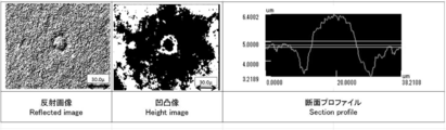
- An example of a ring-shaped dent defect in the present invention is shown in FIG.
- the ring-shaped dent defect has a ring-shaped portion where the film thickness is reduced from the periphery, and has a caldera volcanic cross-sectional shape in which the center surrounded by the ring is raised.
- the laser etching method is a method of forming fine lines by removing unnecessary portions of a conductive film obtained by applying and drying a conductive paste by laser ablation. It is easy to understand that if there is a defect that the conductive film does not exist, such as “Bubble trace” or “Occlusion”, before the laser etching, that part becomes a disconnection defect after etching. it can.
- the ring-shaped dent defect is a relatively large unevenness on the surface of the coating film, but does not necessarily have a portion where the conductive coating does not completely exist. Nevertheless, the portion where the ring-shaped dent defect is present is likely to break the fine line after laser etching.
- This phenomenon is thought to be due to the central convex part of the ring-shaped dent defect being placed in a semi-insulated state in the coating film by the surrounding ring-shaped dent, causing heat accumulation in the central part and causing abnormal ablation. It is done.
- the number of ring-shaped dent defects present in the conductive film is small, and the existence density is essential to be 50 pieces / cm 2 or less, preferably 20 Pieces / cm 2 or less, more preferably 8 pieces / cm 2 or less, still more preferably 3 pieces / cm 2 or less.
- the surface roughness Ra of the portion where no ring-shaped depression exists is preferably 0.1 or more and 1.0 ⁇ m or less, more preferably 0.1 or more and 0.8 ⁇ m or less, and still more preferably 0.8. 1 ⁇ m or more and 0.6 ⁇ m or less.
- the average film thickness of the conductive coating of the present invention is 2 ⁇ m or more and 20 ⁇ m or less, preferably 3 ⁇ m or more and 14 ⁇ m or less, and more preferably 4 ⁇ m or more and 11 ⁇ m or less.
- the conductive coating of the present invention having few ring-shaped dent defects is obtained by using a conductive paste composed of a conductive filler, a binder resin, and a solvent at a low temperature and for a sufficiently long time, for example, at about 60 ° C. to 100 ° C. for 60 minutes to 300 minutes. It can be realized by drying and solidifying under the condition of the degree. However, it is virtually impossible to spend such a long time in the process of drying the conductive paste in the actual manufacturing process.
- a conductive film with few ring-shaped dent defects which is the object of the present invention, can be obtained by at least one of the following methods (1) to (3).
- the conductive paste of the present invention comprises at least (A) a polymer binder resin, (B) Metal powder having an average particle diameter of 0.3 ⁇ m or more and 6 ⁇ m or less (C) Organic solvent (D) Silicon dioxide particles having an average particle diameter of 5 nm or more and 200 nm or less are contained.
- the silicon dioxide particles form a network in the paste dry coating film and have an action of promoting solvent volatilization in the paste layer. More preferably, by using a mixed solvent satisfying the specific conditions as the solvent, the volatilization of the solvent is further promoted, and as a result, the movement of the solvent becomes smooth even after the paste coating film reaches the reduced rate drying.
- the conductive paste of the present invention comprises at least metal particles (B) having an average particle size of 0.3 ⁇ m or more and 6 ⁇ m or less. Carbon particles (E) having an average particle diameter of 5 nm or more and 200 nm or less, Polymer binder resin (A), Organic solvent (C) Containing.
- the carbon particles form a network in the dry coating film and have an action of promoting solvent volatilization in the paste layer. More preferably, by using a mixed solvent satisfying the specific conditions as the solvent, the volatilization of the solvent is further promoted, and as a result, the movement of the solvent becomes smooth even after the paste coating film reaches the reduced rate drying.
- the conductive paste of the present invention comprises at least (B) silver particles having an average particle size of 0.3 ⁇ m or more and 6 ⁇ m or less, and (G) carbon or silicon dioxide particles having an average particle size of 5 nm or more and 200 nm or less, (H) inorganic particles having an average particle size of 0.1 ⁇ m or more and 3 ⁇ m or less, (A) a polymer binder resin, (E) Contains a solvent.
- (B) silver particles having an average particle size of 0.3 ⁇ m or more and 6 ⁇ m or less and
- G) carbon or silicon dioxide particles having an average particle size of 5 nm or more and 200 nm or less a polymer binder resin
- E Contains a solvent.
- in addition to (G) carbon or silicon dioxide particles (H) inorganic particles having an average particle size of 0.1 ⁇ m or more and 3 ⁇ m or less form a network in the dry paint film of the paste, Has the effect of promoting solvent volatilization.
- the volatilization of the solvent is further promoted, and as a result, the movement of the solvent becomes smooth even after the paste coating film reaches the reduced rate drying.
- L / S 50/50 ⁇ m or less.
- the residual solvent hardly remains inside the coating film, and as a result, the adhesion is improved.
- flushing due to rapid evaporation and divergence of the residual solvent during laser etching is prevented, a positive effect on productivity can be obtained.
- the type of binder resin (A) in the present invention is not particularly limited as long as it is a thermoplastic resin, but polyester resin, epoxy resin, phenoxy resin, butyral resin, polyamide resin, polyamideimide resin, polycarbonate resin, polyurethane resin, phenol resin, Acrylic resin, polystyrene, styrene-acrylic resin, styrene-butadiene copolymer, phenolic resin, polyethylene resin, polycarbonate resin, phenolic resin, alkyd resin, styrene-acrylic resin, styrene-butadiene copolymer resin, polysulfone resin, poly Examples include ether sulfone resin, vinyl chloride-vinyl acetate copolymer resin, ethylene-vinyl acetate copolymer, polystyrene, silicone resin, fluorine resin, and the like.
- a mixture of two or more kinds can be used.
- one or a mixture of two or more selected from the group consisting of a polyester resin, a polyurethane resin, an epoxy resin, a phenoxy resin, a vinyl chloride resin, and a fiber derivative resin is preferable.
- these resins it is preferable to use at least one of a polyester resin, a polyurethane resin containing a polyester component as a copolymer component (hereinafter sometimes referred to as a polyester polyurethane resin), an epoxy resin, and a phenoxy resin. More preferable as a binder resin.
- One of the advantages of using a polyester resin as the binder resin in the present invention is the high degree of freedom in molecular design.
- the dicarboxylic acid and glycol components constituting the polyester resin can be selected and the copolymerization component can be freely changed, and the functional group can be easily added in the molecular chain or at the molecular end. For this reason, the characteristics of the resin such as the glass transition temperature of the polyester resin to be obtained and the affinity with other components blended in the base material and the conductive paste can be appropriately adjusted.
- trivalent or higher carboxylic acids such as trimellitic anhydride and pyromellitic anhydride, unsaturated dicarboxylic acids such as fumaric acid, and / or 5-sulfoisophthalic acid sodium salt, etc., as long as the effects of the invention are not impaired.
- the sulfonic acid metal base-containing dicarboxylic acid may be used as a copolymerization component.
- trivalent or higher polyols such as trimethylolethane, trimethylolpropane, glycerin, pentaerythritol, polyglycerin and the like may be used in combination as a copolymerization component as long as the effects of the invention are not impaired.
- the polyester resin used as the binder resin in the present invention is 10 mol of aliphatic dicarboxylic acid among all acid components constituting the polyester resin from the viewpoints of adhesion and compatibility with other resins used in combination and thermal shock resistance. % Or more is preferably copolymerized, more preferably 20 mol% or more, still more preferably 30 mol% or more. If the copolymerization ratio of the aromatic dicarboxylic acid component is too high, the glass transition temperature of the resulting polyester resin will be 60 ° C or higher, resulting in poor storage stability due to poor compatibility with the resin used together, and a straight line of laser etching processing. There is a possibility that the adhesiveness will deteriorate and the adhesiveness of the resulting conductive thin film after laser etching will deteriorate.
- polyurethane resin as the binder resin in the present invention.
- glass transition can be achieved by selecting appropriate components as copolymer components that make up polyurethane resins, and by adding functional groups in the molecular chain or at the molecular ends. Resin properties such as temperature and affinity with other components blended in the substrate and the conductive paste can be appropriately adjusted.
- the copolymer component of the polyurethane resin is not particularly limited, but is preferably a polyester polyurethane resin using a polyester polyol as a copolymer component from the viewpoint of freedom of design, heat and humidity resistance, and maintenance of durability.
- a polyester polyol what is a polyol among the polyester resins which can be used as binder resin in the above-mentioned this invention can be mentioned.
- the polyurethane resin used as the binder resin in the present invention can be obtained, for example, by a reaction between a polyol and a polyisocyanate.
- the polyisocyanate that can be used as a copolymerization component of the polyurethane resin include 2,4-tolylene diisocyanate, 2,6-tolylene diisocyanate, p-phenylene diisocyanate, 4,4′-diphenylmethane diisocyanate, m-phenylene diisocyanate.
- a compound having a functional group capable of reacting with isocyanate can be copolymerized as necessary.
- the functional group capable of reacting with isocyanate is preferably a hydroxyl group or an amino group, and may have either one or both.
- dimethylolbutanoic acid dimethylolpropionic acid
- 1,2-propylene glycol 1,2-butylene glycol, 1,3-butylene glycol, 2,3-butylene glycol, 2,2 -Dimethyl-1,3-propanediol, 3-methyl-1,5-pentanediol, 2,2,4-trimethyl-1,3-pentanediol, 2-ethyl-1,3-hexanediol, 2,2 -Dimethyl-3-hydroxypropyl-2 ', 2'-dimethyl-3'-hydroxypropanoate, 2-normalbutyl-2-ethyl-1,3-propanediol, 3-ethyl-1,5-pentanediol, 3-propyl-1,5-pentanediol, 2,2-diethyl-1,3-propanediol, 3-octyl-1,5-pentanediol,
- Examples of the epoxy resin used as the binder resin in the present invention include glycidyl ether types such as bisphenol A glycidyl ether, bisphenol S glycidyl ether, novolak glycidyl ether, and bisbrominated bisidyl, hexahydrophthalic acid glycidyl ester, and dimer acid glycidyl ester.
- Examples include glycidyl ester type, triglycidyl isocyanurate, or alicyclic or aliphatic epoxides such as 3,4-epoxycyclohexylmethyl carboxylate, epoxidized polybutadiene, and epoxidized soybean oil. You may use the above together.
- bisphenol A glycidyl ether is preferable from the viewpoint of durability of the coating film, and more preferably one having two or more glycidyl ether groups in one molecule.
- the number average molecular weight of the binder resin in the present invention is not particularly limited, but the number average molecular weight is preferably 5,000 to 60,000, more preferably 10,000 to 40,000. If the number average molecular weight is too low, it is not preferable in terms of durability and heat and humidity resistance of the formed conductive thin film. On the other hand, if the number average molecular weight is too high, the cohesive strength of the resin increases and the durability as a conductive thin film is improved, but the suitability for laser etching is significantly deteriorated.
- the glass transition temperature of the binder resin in the present invention is preferably 120 ° C. or lower, and more preferably 100 ° C. or lower. When the glass transition temperature is low, the linearity after laser etching becomes good, and the substrate adhesion after laser etching tends to be good.
- the acid value of the binder resin in the present invention is not particularly limited. However, if the acid value is too high, the water-absorbing property of the formed conductive thin film is increased and the hydrolysis of the binder resin is promoted by the catalytic action of the carboxyl group. There is a possibility that the reliability of the conductive thin film may be reduced. Hydrolysis is more prominent at lower glass transition temperatures. Therefore, by setting the acid value of the binder resin to a low acid value, preferably less than 400 eq / ton, more preferably 300 eq / ton or less, the conductive resin has both high reliability of the conductive thin film and linearity and adhesion of laser etching. Led to the realization of a sex paste.
- the metal powder (B) used in the present invention is plated with noble metal powder such as silver powder, gold powder, platinum powder and palladium powder, base metal powder such as copper powder, nickel powder, aluminum powder and brass powder, or noble metal such as silver.
- noble metal powder such as silver powder, gold powder, platinum powder and palladium powder
- base metal powder such as copper powder, nickel powder, aluminum powder and brass powder
- noble metal such as silver.
- An alloyed base metal powder and the like, for example, silver-coated copper powder can be exemplified.
- These metal powders may be used alone or in combination. Among these, in consideration of conductivity, stability, cost, etc., silver powder alone and / or silver-plated copper powder plated with silver or silver-plated alloy powder is preferred.
- the shape of the metal powder used in the present invention is not particularly limited.
- Examples of conventionally known metal powder shapes include flakes (flakes), spheres, dendrites (dendrites), and spherical primary particles described in JP-A-9-306240.
- the center diameter (D50) of the metal powder used in the present invention is preferably 6 ⁇ m or less, more preferably 4 ⁇ m or less, and even more preferably 2 ⁇ m or less.
- the center diameter (D50) of the metal powder used in the present invention is preferably 6 ⁇ m or less, more preferably 4 ⁇ m or less, and even more preferably 2 ⁇ m or less.
- the lower limit of the center diameter of the metal powder is not particularly limited, but from the viewpoint of cost and the particle diameter becomes finer, it tends to aggregate and consequently difficult to disperse. Therefore, the center diameter is preferably 80 nm or more, 0.3 ⁇ m or more It is more preferable that When the center diameter is smaller than 80 nm, the cohesive force of the metal powder increases, the laser etching processing suitability deteriorates, and it is not preferable from the viewpoint of cost.
- the central diameter (D50) is the particle diameter ( ⁇ m) at which the cumulative value is 50% in the cumulative distribution curve (volume) obtained by some measurement method.
- the cumulative distribution curve is measured in the total reflection mode using a laser diffraction / scattering particle size distribution measuring apparatus (MICROTRAC HRA manufactured by Nikkiso Co., Ltd.).
- the content of the metal powder is preferably 400 parts by mass or more and more preferably 560 parts by mass or more with respect to 100 parts by mass of the binder resin from the viewpoint that the conductivity of the formed conductive thin film is good. Moreover, from a viewpoint that content of a component is favorable in adhesiveness with a base material, 1,900 mass parts or less are preferable with respect to 100 mass parts of binder resin, and 1,230 mass parts or less are more preferable. Silver particles (silver powder) can be preferably used in the present invention.
- the organic solvent (C) that can be used in the present invention is not particularly limited, but from the viewpoint of keeping the volatilization rate of the organic solvent within an appropriate range, the boiling point is preferably 100 ° C. or more and less than 300 ° C., more preferably. Has a boiling point of 150 ° C. or higher and lower than 280 ° C.
- the conductive paste of the present invention is typically prepared by dispersing a binder resin, a metal powder, an organic solvent and other components as necessary with a three-roll mill or the like. If the amount is too large, the solvent volatilizes during dispersion, and the component ratio of the conductive paste may change. On the other hand, if the boiling point of the organic solvent is too high, a large amount of the solvent may remain in the coating film depending on the drying conditions, which may cause a decrease in the reliability of the coating film.
- the organic solvent that can be used in the present invention is preferably one in which the binder resin is soluble and the metal powder can be well dispersed.
- Specific examples include ethyl diglycol acetate (EDGAC), butyl glycol acetate (BMGAC), butyl diglycol acetate (BDGAC), cyclohexanone, toluene, isophorone, ⁇ -butyrolactone, benzyl alcohol, Exson Chemical's Solvesso 100, 150, 200, a mixture of dimethyl ester of propylene glycol monomethyl ether acetate, adipic acid, succinic acid and glutaric acid (for example, DBE manufactured by DuPont Co., Ltd.), terpionol, etc.
- blending of binder resin EDGAC, BMGAC, BDGAC, and mixed solvents thereof from the viewpoint of excellent solubility of components, moderate solvent volatility during continuous printing, and good suitability for printing by screen printing methods, etc. Preferred.
- the content of the organic solvent is preferably 5 to 40 parts by weight, more preferably 10 to 35 parts by weight, based on 100 parts by weight of the total paste. If the content of the organic solvent is too high, the paste viscosity becomes too low, and it tends to cause sagging during fine line printing. On the other hand, if the content of the organic solvent is too low, the viscosity as a paste becomes extremely high, and, for example, the screen printability when forming the conductive thin film is remarkably lowered, and the film thickness of the formed conductive thin film is The thickness may increase and laser etching processability may decrease.
- the type of silicon dioxide particles (D) used in the conductive paste of the present invention is not limited in any way, but silica, fumed silica (for example, Aerosil manufactured by Nippon Aerosil Co., Ltd.), colloidal silica, or the like can be used.
- silica fumed silica (for example, Aerosil manufactured by Nippon Aerosil Co., Ltd.), colloidal silica, or the like can be used.
- silicon dioxide particles are not used, the filler filling property in the conductive thin film is poor, the solvent bumps, and a ring-shaped dent is likely to occur.
- silicon dioxide particles by using silicon dioxide particles, the filler filling property in the conductive thin film becomes high, so that the solvent is difficult to bump and the ring-shaped dent can be suppressed.
- the average primary particle diameter of the silicon dioxide particles used in the present invention is preferably 200 nm or less, more preferably 50 nm or less, and even more preferably 20 ⁇ m or less.
- the particle diameter of the silicon oxide particles is large, the filler filling property is poor, and ring-shaped dents cannot be suppressed.
- the silicon dioxide particle used for this invention it is preferable to mix
- the carbon particles (E) used in the conductive paste of the present invention ketjen black, acetylene black, furnace black, channel black, lamp black and the like can be used.
- carbon particles are not used, the filler filling property in the conductive thin film is poor, and the solvent pushes up the surface layer of the coating film during drying, which easily causes ring-shaped dents.
- the filler filling property in the conductive thin film becomes high, the solvent paths are dispersed and uniform, and are not concentrated in one place, so that ring-shaped dents can be suppressed.
- the average primary particle diameter of the carbon particles used in the present invention is preferably 200 nm or less, more preferably 50 nm or less, and further preferably 20 ⁇ m or less.
- the particle diameter of the silicon oxide particles is large, the filler filling property is poor, and ring-shaped dents cannot be suppressed.
- carbon particles of the present invention As content of the carbon particle used for this invention, it is preferable to mix
- the carbon particles of the present invention also have an action as a laser light absorber.
- inorganic substances include silicon carbide, boron carbide, titanium carbide, zirconium carbide, hafnium carbide, vanadium carbide, tantalum carbide, niobium carbide, tungsten carbide, chromium carbide, molybdenum carbide, calcium carbide, diamond carbon lactam, and other carbides; boron nitride , Various nitrides such as titanium nitride and zirconium nitride, various borides such as zirconium boride; various oxides such as titanium oxide (titania), calcium oxide, magnesium oxide, zinc oxide, copper oxide and aluminum oxide; calcium titanate , Various titanate compounds such as magnesium titanate and strontium titanate; sulfides such as molybdenum disulfide; sulfates such as barium sulfate and magnesium s
- an inorganic ion scavenger can be preferably used as the inorganic particles blended in the conductive paste of the present invention.
- the inorganic ion scavenger is an inorganic particle having a primary particle size of submicron, and is a hydrotalcite hybridized with a metal oxide or hydroxide. Examples of commercially available products include IXE and IXEPLAS manufactured by Toagosei Co., Ltd.
- the average particle size of the inorganic particles used in the present invention is 0.1 ⁇ m or more and 3 ⁇ m or less, preferably. It is 1 ⁇ m or more and 1.2 ⁇ m, more preferably 0.13 ⁇ m or more and 0.85 ⁇ m or less.
- the particle diameter of the inorganic particles is large, the filler filling property is poor, and ring-shaped dents cannot be suppressed.
- the inorganic particle used for this invention it is preferable to mix
- the laser paste (F) may be added to the conductive paste of the present invention.
- the laser light absorbent is an additive having strong absorption at the wavelength of the laser light, and the laser light absorbent itself may be conductive or non-conductive.
- a YAG laser having a fundamental wave wavelength of 1064 nm is used as a light source
- a dye and / or pigment having strong absorption at a wavelength of 1064 nm can be used as a laser light absorber.
- the conductive thin film of the present invention absorbs laser light with high efficiency, and the volatilization and thermal decomposition of the binder resin due to heat generation is promoted, and as a result, the suitability for laser etching is improved.
- laser light absorbers examples of those having conductivity include carbon-based fillers such as carbon black and graphite powder.
- carbon-based fillers such as carbon black and graphite powder.
- ketjen black, acetylene black, furnace black, channel black, lamp black and the like can be raised.
- ketjen black is preferable from the viewpoint of conductivity and laser absorption.
- the compounding of the carbon-based filler has the effect of increasing the conductivity of the conductive thin film of the present invention. For example, since carbon black has an absorption wavelength in the vicinity of 1060 nm, it has a wavelength of 1064 nm such as YAG laser and fiber laser.
- the conductive thin film When irradiated with laser light, the conductive thin film absorbs laser light with high efficiency, so the sensitivity to laser light irradiation increases, and it is good even when the scanning speed of laser irradiation is increased and / or when the laser light source is low power
- the effect that laser etching processing suitability can be obtained can be expected.
- the content of the carbon-based filler is preferably 0.1 to 5 parts by weight, more preferably 0.3 to 2 parts by weight with respect to 100 parts by weight of the metal powder. When the blending ratio of the carbon filler is too low, the effect of increasing the conductivity and the effect of increasing the sensitivity to laser light irradiation are small.
- the conductivity of the conductive thin film tends to be lowered, and further, the resin is adsorbed to the void portion of the carbon and the adhesion with the substrate is lowered. Dots may occur.
- non-conductive laser light absorbers examples include conventionally known dyes, pigments, and infrared absorbers. More specifically, azo dyes, metal complex azo dyes, pyrazolone azo dyes, naphthoquinone dyes, anthraquinone dyes, phthalocyanine dyes, carbonium dyes, quinoneimine dyes, methine dyes, cyanine dyes, squarylium dyes, pyrylium salts, metal thiolate complexes, etc.
- the dyes and pigments include black pigments, yellow pigments, orange pigments, brown pigments, red pigments, purple pigments, blue pigments, green pigments, fluorescent pigments, metal powder pigments, and polymer-bonded pigments.
- infrared absorbers examples include NIR-IM1, which is a diimonium salt type infrared absorber, and NIR-AM1, an aminium salt type (both manufactured by Nagase ChemteX Corporation).
- NIR-IM1 which is a diimonium salt type infrared absorber
- NIR-AM1 an aminium salt type (both manufactured by Nagase ChemteX Corporation).
- These non-conductive laser light absorbers are contained in an amount of 0.01 to 5 parts by weight, preferably 0.1 to 2 parts by weight.
- the blending ratio of the non-conductive laser light absorber is too low, the effect of increasing the sensitivity to laser light irradiation is small.
- the blending ratio of the non-conductive laser light absorber is too high, the conductivity of the conductive thin film may be lowered, and the color of the laser light absorber becomes remarkable, which may not be preferable depending on the application.
- the conductive paste of the present invention includes a thixotropic agent, an antifoaming agent, a flame retardant, a tackifier, a hydrolysis inhibitor, a leveling agent, a plasticizer, an antioxidant, an ultraviolet absorber, a flame retardant, and a pigment.
- Dyes can be blended.
- a carbodiimide, an epoxy, etc. can also be mix
- a curing agent (G) that can react with the binder resin may be blended to such an extent that the effects of the present invention are not impaired.
- a curing agent By adding a curing agent, there is a possibility that the curing temperature becomes high and the load of the production process may increase.
- the heat and humidity resistance of the coating film can be improved by crosslinking caused by heat generated during coating film drying or laser etching. .
- the type of the curing agent capable of reacting with the binder resin of the present invention is not limited, but an isocyanate compound and / or an epoxy resin is particularly preferable from the viewpoint of adhesion, flex resistance, curability, and the like. Furthermore, regarding the isocyanate compound, it is preferable to use a blocked isocyanate group since the storage stability is improved.
- curing agents other than isocyanate compounds include known compounds such as amino resins such as methylated melamine, butylated melamine, benzoguanamine, and urea resin, acid anhydrides, imidazoles, and phenol resins. These curing agents can be used in combination with a known catalyst or accelerator selected according to the type.
- the blending amount of the curing agent is blended to such an extent that the effects of the present invention are not impaired, and is not particularly limited, but is 0.5 to 50 parts by mass with respect to 100 parts by mass of the binder resin. It is preferably 1 to 30 parts by mass, more preferably 2 to 20 parts by mass.
- aromatic diisocyanates such as tetramethylene diisocyanate and hexamethylene diisocyanate
- aromatic diisocyanates such as toluene diisocyanate, diphenylmethane diisocyanate, xylylene diisocyanate, hydrogenated diphenylmethane diisocyanate, hydrogenated xylylene diisocyanate, dimer acid diisocyanate, isophorone diisocyanate, etc.
- Alicyclic diisocyanates, or trimers of these isocyanate compounds, and excess amounts of these isocyanate compounds such as ethylene glycol, propylene glycol, trimethylolpropane, glycerin, sorbitol, ethylenediamine, monoethanolamine, diethanolamine, triethanolamine
- Low molecular active hydrogen compounds such as Polyester polyols, polyether polyols, terminal isocyanate group-containing compounds obtained by reacting a polymeric active hydrogen compound such as polyamides and the like.
- isocyanate group blocking agent examples include phenols such as phenol, thiophenol, methylthiophenol, ethylthiophenol, cresol, xylenol, resorcinol, nitrophenol, and chlorophenol; oximes such as acetoxime, methyl ethyl ketoxime, and cyclohexanone oxime.
- Alcohols such as methanol, ethanol, propanol and butanol; halogen-substituted alcohols such as ethylene chlorohydrin and 1,3-dichloro-2-propanol; tertiary alcohols such as t-butanol and t-pentanol ; Lactams such as ⁇ -caprolactam, ⁇ -valerolactam, ⁇ -butyrolactam, ⁇ -propylolactam, pyrazole blocking agents, and other aromatic amines, imi S, acetylacetone, acetoacetic ester, active methylene compounds such as malonic acid ethyl ester, mercaptans, imines, imidazoles, ureas, diaryl compounds, sodium bisulfite, etc. can be mentioned. Of these, oximes, imidazoles, amines, and pyrazoles are particularly preferable from the viewpoint of curability.
- Examples of the epoxy compound used as a curing agent in the present invention include glycidyl ether types such as bisphenol A glycidyl ether, bisphenol S glycidyl ether, novolak glycidyl ether, and bromo bromide, hexahydrophthalic acid glycidyl ester, and dimer acid glycidyl ester.
- Examples include glycidyl ester type, triglycidyl isocyanurate, or alicyclic or aliphatic epoxides such as 3,4-epoxycyclohexylmethyl carboxylate, epoxidized polybutadiene, and epoxidized soybean oil. You may use the above together.
- bisphenol A glycidyl ether is most preferable, and among them, those having a molecular weight of less than 5000 and having two or more glycidyl ether groups in one molecule are more preferable.
- the viscosity of the conductive paste of the present invention is not particularly limited, and may be appropriately adjusted according to the method for forming the coating film.
- the viscosity of the conductive paste is preferably 200 dPa ⁇ s or more when measured with a BH viscometer at 20 rpm at the printing temperature.
- it is 400 dPa * s or more, Most preferably, it is 600 dPa * s or more.
- the upper limit is not particularly limited, but if the viscosity is too high, the thickness of the conductive thin film becomes too thick, and the suitability for laser etching may deteriorate.
- the conductive paste of the present invention preferably has an F value of 60 to 95%, more preferably 75 to 95%.
- the filler mass part referred to here is the mass part of the conductive powder, and the solid mass part is a mass part of components other than the solvent, and includes all of the conductive powder, the binder resin, and other curing agents and additives. If the F value is too low, a conductive thin film showing good conductivity cannot be obtained.
- the conductive powder refers to both metal powder and non-metal conductive powder.
- the conductive paste of the present invention is formed by applying or printing the conductive paste of the present invention on a substrate to form a coating film, and then evaporating the organic solvent contained in the coating film and drying the coating film.
- the method for applying or printing the conductive paste on the substrate is not particularly limited, but printing by the screen printing method is simple in the process and the technology that is widely used in the industry for forming an electric circuit using the conductive paste It is preferable from the point.
- the conductive paste can be applied or printed on a portion slightly wider than the portion of the conductive thin film that is ultimately required as an electric circuit, reducing the load of the laser etching process and improving the efficiency of the electric circuit of the present invention. From the viewpoint of forming, it is preferable.
- a material excellent in dimensional stability is preferably used as the substrate on which the conductive paste of the present invention is applied.
- a film made of a material having excellent flexibility such as polyethylene terephthalate, polyethylene naphthalate, polybutylene terephthalate, or polycarbonate can be used.
- inorganic materials, such as glass can also be used as a base material.
- the thickness of the substrate is not particularly limited, but is preferably 12.5 ⁇ m to 1 mm, and more preferably 25 ⁇ m to 0.5 mm. When considering the mechanical characteristics, shape stability, handleability, etc. of the pattern forming material, the above-mentioned range is obtained.
- the adhesion between the conductive thin film and the substrate can be improved.
- the physical treatment method include a sand blast method, a wet blast method in which a liquid containing fine particles is sprayed, a corona discharge treatment method, a plasma treatment method, an ultraviolet ray or vacuum ultraviolet ray irradiation treatment method, and the like.
- chemical treatment methods include strong acid treatment methods, strong alkali treatment methods, oxidizing agent treatment methods, and coupling agent treatment methods.
- the base material may have a transparent conductive layer.
- the conductive thin film of the present invention can be laminated on the transparent conductive layer.
- the material of the transparent conductive layer is not particularly limited, and examples thereof include an ITO film mainly composed of indium tin oxide and a silver nanowire film composed of nano-sized linear silver.
- the transparent conductive layer is not limited to the one formed on the entire surface of the base material, but can also be one obtained by removing a part of the transparent conductive layer by etching or the like.
- the step of evaporating the organic solvent is preferably performed at room temperature and / or under heating.
- the heating temperature is preferably 80 ° C. or higher, more preferably 100 ° C. or higher, and further preferably 110 ° C. or higher. Further, from the viewpoint of heat resistance of the underlying transparent conductive layer and energy saving in the production process, the heating temperature is preferably 150 ° C. or lower, more preferably 135 ° C. or lower, and further preferably 130 ° C. or lower.
- the curing reaction proceeds when the step of evaporating the organic solvent is performed under heating.
- the thickness of the conductive thin film of the present invention may be set to an appropriate thickness according to the application used.
- the thickness of the conductive thin film is preferably 3 ⁇ m or more and 30 ⁇ m or less, more preferably 4 ⁇ m from the viewpoint that the conductivity of the conductive thin film after drying is good and the suitability for laser etching processing is good. As mentioned above, it is 20 micrometers or less, More preferably, they are 4 micrometers or more and 10 micrometers or less. If the conductive thin film is too thin, there is a possibility that desired conductivity as a circuit cannot be obtained. If the film thickness is too thick, an excessive amount of laser irradiation is required for laser etching, which may damage the substrate.
- the conductive thin film tends to be etched easily, and a short circuit between lines due to insufficient etching or disconnection due to excessive etching tends to occur. For this reason, it is better that the variation in film thickness is small.
- the surface roughness Ra of the conductive thin film of the present invention is preferably 0.7 ⁇ m or less, more preferably 0.5 ⁇ m or less, and still more preferably 0.4 ⁇ m or less. If the surface roughness Ra is too high, the etching end portion of the conductive thin film is likely to be jagged, and there is a possibility that a short circuit between lines or disconnection due to excessive etching is likely to occur. Since the surface roughness Ra is strongly influenced by the paste composition (particularly binder type and silver powder type), paste viscosity, and screen printing conditions, it is necessary to adjust and control them appropriately.
- the electric circuit of the present invention removes a part of the conductive thin film from the substrate by irradiating at least a part of the conductive thin film formed on the substrate with the conductive paste of the present invention. It is an electric circuit which has the wiring site
- the pattern formation process can be a dry process, and no waste liquid containing metal components is generated, so there is no need for waste liquid treatment and the environment is friendly. It can be said that it is a process.
- the process is simple, investment in manufacturing equipment can be suppressed, and maintenance and management of the manufacturing equipment after operation is easy.
- the method for forming the conductive thin film on the substrate with the conductive paste is not particularly limited, but can be performed by printing or painting.
- the laser beam irradiation method is not particularly limited, but a laser etching processing apparatus that has been widely used in recent years, or a device that further improves the dimensional accuracy thereof can be used. Since the laser etching processing apparatus can directly use data produced by image processing application software such as CAD for laser processing, it is very easy to switch manufacturing patterns. This can be cited as one of the advantages over the conventional pattern formation by the screen printing method.
- the conductive thin film of the present invention preferably has strong absorption at the wavelength of the irradiated laser light. Therefore, it is preferable to select a laser species having energy in a wavelength region where any of the components constituting the conductive thin film of the present invention has strong absorption.
- Examples of laser types include excimer laser (fundamental wavelength is 193 to 308 nm), YAG laser (fundamental wave is 1064 nm), fiber laser (fundamental wave is 1060 nm), and semiconductor laser. Basically, there is no problem no matter what type of laser is used. By selecting a laser species that matches the absorption wavelength region of any constituent of the conductive thin film and that can be irradiated with a wavelength that the substrate does not have strong absorption, the conductive thin film at the laser light irradiation site is selected. Can be efficiently removed, and damage to the substrate can be avoided.
- the laser type of the irradiated laser species is preferably 190 nm to 1100 nm, and more preferably 500 nm to 1000 nm.
- a YAG laser or a fiber laser may be used. Since the base material has no absorption at the wavelength of the fundamental wave, it is particularly preferable in that the base material is not easily damaged.
- the laser output and frequency are not particularly limited, but the conductive thin film at the laser light irradiation site can be removed with an etching width of 10 to 40 ⁇ m and adjusted so that the underlying substrate is not damaged.
- the laser output is preferably adjusted as appropriate within a range of 0.5 to 100 W, a frequency of 10 to 1000 kHz, and a pulse width of 1000 ns or less. If the laser output is too low, removal of the conductive thin film tends to be insufficient, but such tendency can be avoided to some extent by reducing the laser scanning speed or increasing the number of scans.
- the laser output is preferably adjusted appropriately within a range of 0.5 to 20 W, a frequency of 10 to 800 kHz, and a pulse width of 800 ns or less, more preferably 0.5 to 12 W, a frequency of 10 to 600 kHz, and a pulse width of 600 ns. It is as follows.
- the lower limit of the pulse width is preferably 1 fs or more, more preferably 1 ps or more, and most preferably 1 ns or more.
- the scanning speed of the laser beam is preferably as high as possible from the viewpoint of improving the production efficiency by reducing the tact time. Specifically, it is preferably 1000 mm / s or more, more preferably 1500 mm / s or more, and further preferably 2000 mm / s or more. .
- the upper limit is not particularly limited, but is about 10,000 mm / s or less. If the scanning speed is too slow, not only the production efficiency is lowered, but the conductive thin film and the substrate may be damaged by the thermal history. Although the upper limit of the processing speed is not particularly defined, if the scanning speed is too high, the removal of the conductive thin film at the laser light irradiation site may be incomplete and the circuit may be short-circuited.
- Laser beam scanning may be performed by either moving a laser beam projectile, moving an object to be irradiated with laser light, or a combination of both, for example, using an XY stage. Further, the laser beam can be scanned by changing the irradiation direction of the laser beam using a galvanometer mirror or the like.
- the energy density per unit area can be increased by using a condensing lens (such as an achromatic lens) at the time of laser light irradiation.
- a condensing lens such as an achromatic lens
- the advantage of this method is that the energy density per unit area can be increased compared to the case of using a mask, so laser etching can be performed at a high scanning speed even with a low-power laser oscillator. The point that becomes possible.
- the focal length must be adjusted according to the film thickness applied to the substrate, but it can be adjusted so that the substrate is not damaged and the predetermined conductive thin film pattern can be removed and removed. preferable.
- laser beam scanning is repeated a plurality of times in the same pattern. Even if there is an incompletely removed conductive thin film portion in the first scan, or even if the component constituting the removed conductive thin film is attached to the substrate again, the laser light irradiated portion is scanned multiple times. It is possible to completely remove the conductive thin film.
- the number of scans is preferably 4 times, more preferably 3 times.
- the upper limit is not particularly limited, it is necessary to pay attention because the periphery of the processed part may be damaged, discolored, and the physical properties of the coating film may be deteriorated by receiving heat history multiple times. Of course, the smaller the number of scans, the better from the viewpoint of production efficiency.
- laser beam scanning is not repeated a plurality of times in the same pattern.
- the smaller the number of scans the better the production efficiency, as long as the properties of the resulting conductive thin film, conductive laminate and electrical circuit are not adversely affected.
- the conductive thin film of the present invention contains expensive conductive powder at a high concentration, it is included in the conductive thin film removed from the base material in view of the total cost required for manufacturing the electric circuit to be manufactured. It is important to collect and reuse the conductive powder.
- a highly profitable processing method can be obtained by providing a high-performance dust collector near the laser beam irradiation site and constructing a system for efficiently collecting the conductive powder.
- the conductive thin film, conductive laminate and / or electric circuit of the present invention can be used as a constituent member of a touch panel.
- the touch panel may be a resistive film type or a capacitive type. Although it can be applied to any touch panel, the paste is suitable for forming a thin line, and therefore can be particularly suitably used for electrode wiring of a capacitive touch panel.
- membrane, or the base material from which they were partially removed by an etching is used. Is preferred.
- the number average molecular weight sample binder resin was dissolved in tetrahydrofuran so that the resin concentration was about 0.5% by weight, and filtered through a polytetrafluoroethylene membrane filter having a pore size of 0.5 ⁇ m to obtain a GPC measurement sample.
- GPC measurement of a resin sample using tetrahydrofuran as a mobile phase, a gel permeation chromatograph (GPC) Prominence manufactured by Shimadzu Corporation, and a differential refractometer (RI meter) as a detector at a column temperature of 30 ° C. and a flow rate of 1 ml / min. was done.
- the number average molecular weight was a standard polystyrene equivalent value, and was calculated by omitting a portion corresponding to a molecular weight of less than 1000.
- GPC column shodex KF-802, 804L and 806L manufactured by Showa Denko KK were used.
- the acid value sample binder resin 0.2 g was precisely weighed and dissolved in 20 ml of chloroform. Subsequently, titration was performed with 0.01 N potassium hydroxide (ethanol solution) using a phenolphthalein solution as an indicator. The unit of the acid value was eq / ton, that is, the equivalent per 1 ton of the sample.
- tons are metric tons.
- Resin Composition A sample binder resin was dissolved in chloroform-d, and a resin composition was determined by 1H-NMR analysis using a 400 MHz-NMR apparatus manufactured by VARIAN.
- conductive laminate test piece A 400-mesh stainless steel screen was used for each of the PET film (Lumirror S manufactured by Toray Industries, Inc.) and ITO film (KH150 manufactured by Oike Kogyo Co., Ltd.) that had been annealed to a thickness of 100 ⁇ m.
- a conductive paste was printed by a screen printing method to form a solid coating pattern having a width of 25 mm and a length of 450 mm, and then heated at 130 ° C. for 30 minutes in a hot-air circulating drying furnace to obtain a conductive laminate test piece. .
- the coating thickness at the time of printing was adjusted so that the dry film thickness was 4 to 10 ⁇ m.
- the sheet resistance and film thickness of the conductive laminate test piece were measured, and the specific resistance was calculated.
- a gauge stand ST-022 manufactured by Ono Sokki Co., Ltd.
- the sheet resistance was measured for four test pieces using MILLIOHMMETER 4338B (manufactured by HEWLETT PACKARD), and the average value was used.
- the range that can be detected by this milliohm meter is 1 ⁇ 10 ⁇ 2 ( ⁇ ⁇ cm) or less, and a specific resistance of 1 ⁇ 10 ⁇ 2 ( ⁇ ⁇ cm) or more is outside the measurement limit.
- Moisture and heat resistance test The conductive laminate test piece was heated at 80 ° C. for 300 hours, then heated at 85 ° C. and 85% RH (relative humidity) for 300 hours, and then allowed to stand at room temperature for 24 hours, after which various evaluations were performed.
- a conductive paste was printed in a 2.5 ⁇ 10 cm rectangle on a polyester substrate (Lumirror S (thickness: 100 ⁇ m) manufactured by Toray Industries, Inc.) by a screen printing method.
- Screen plate is 400 mesh, wire diameter is 18 ⁇ m, calendered, stainless screen with emulsion thickness of 10 ⁇
- printing machine is SSA-TF150E manufactured by Tokai Shoji Co., Ltd.
- printing conditions are squeegee speed 100mm / s, scraper speed 75mm / s, indentation Amount 1.0 mm / s, clearance 1.5 mm, squeegee pressure 0.4 MPa, squeegee angle 75 degrees, squeegee hardness 80 degrees.
- a conductive thin film was obtained by drying at 130 ° C. for 30 minutes in a hot-air circulating drying oven.
- the paste was diluted and adjusted so that the film thickness was 5 to 7 ⁇ m.
- laser etching is performed on the conductive thin film prepared by the above method to produce 10 patterns having four straight portions with a length of 50 mm as shown in FIG. .
- the laser etching process was carried out by using a fiber laser (wavelength: 1064 nm) as a laser light source, adjusting a frequency of 300 kHz, a scanning speed of 2500 mm / s, a pulse width of 15 ns, and an output appropriately.
- a fiber laser wavelength: 1064 nm
- Laser etching process suitability evaluation (1) Conductivity between both ends of fine wire
- an evaluation was made based on whether or not conduction between both ends of the thin wire was ensured. Specifically, a tester is applied to each of the terminals 1a and 1c, between the terminals 2a and 2c, between the terminals 3a and 3c, and between the terminals 4a and 4c. Judged. In addition, since 10 test pieces were produced and there were 4 pieces per piece, evaluation was performed with 40 fine wires. ⁇ : Conduction between both ends of the fine wire is observed for all 40 fine wires. ⁇ : Less than 10 of the 40 thin wires have no conduction between both ends of the thin wire. X: Of the 40 fine wires, 10 or more have no conduction between both ends of the fine wire.
- a conductive thin film was obtained by drying at 130 ° C. for 30 minutes in a hot-air circulating drying oven.
- the number of ring-shaped dents was measured using a laser microscope (Keyence VHX-1000) and judged according to the following evaluation criteria. Number of ring-shaped dents (pieces / cm2) ⁇ 0-5 ⁇ 6-20 ⁇ 21 ⁇ 50 ⁇ 51 or more
- Comparative Example 1 Four types of conductive paste were prepared at the blending ratio shown in Table 1. First, the binder resin is dissolved in an appropriate amount of solvent so that the solid content concentration is 35% by mass, and the resulting binder resin solution, silver powder 1, curing agent, curing catalyst, remaining solvent amount, and other additives are weighed and blended. After premixing, the mixture was dispersed twice by passing through a chilled three-roll kneader. Next, a 795 mesh (stainless mesh filter (line diameter: 16 ⁇ m, mesh size: 16 ⁇ m)) was attached to a paste filter (Protech Corp., PF320A), and the paste was filtered.
- a 795 mesh stainless mesh filter (line diameter: 16 ⁇ m, mesh size: 16 ⁇ m)
- the obtained conductive paste was printed in a predetermined pattern so that the dry film thickness was 17 ⁇ m, and then dried at 120 ° C. for 30 minutes to obtain a conductive thin film.
- the basic physical properties were measured using the obtained conductive thin film, and then laser etching processing was examined. The evaluation results are shown in Table 1.
- Silver powder 1 Aggregated silver powder (D50: 1.3 ⁇ m)
- Silver powder 2 flaky silver powder (D50: 1.3 ⁇ m)
- Silver powder 3 spherical silver powder (D50: 1.3 ⁇ m)
- Silica 1 AEROSIL 300 (primary particle size: 7 nm) manufactured by Nippon Aloesil Carbon 1: Lion ECP600JD (Primary particle size: 34nm)
- Inorganic filler 1 manufactured by Toagosei Co., Ltd.
- Ion supplement agent IXE-PLAS A2 (median diameter: 0.2 ⁇ m)
- Solvent 1 Ethylene glycol monobutyl ether acetate
- Solvent 2 Diethylene glycol monoethyl ether acetate
- Solvent 3 Diethylene glycol monobutyl ether acetate
- Hardener 1 Block isocyanate BI7960 from Baxenden
- Hardener 1 Block isocyanate BI7982 from Baxenden Curing catalyst: Kyodo Pharmaceutical Co., Ltd.
- KS1260 Dispersant 1 Disperbyk167 manufactured by Big Chemie Japan Co., Ltd.
- Additive 1 Carboxylic acid amine salt additive 2: Carboxylic acid.
- ⁇ Application example 1> Using the obtained conductive paste P1, printing was performed so that the dry film thickness was 17 ⁇ m, and the drying temperature and the drying time were changed, and the ring-shaped dent defect, the fine wire both-end conductivity, and the fine wire both-end insulation were evaluated. The results are shown in Tables 2 to 4. It has been shown that when dried at a low temperature for a long time, the dents in the ring are reduced, and the conductivity at both ends of the fine wire and the insulation at both ends of the fine wire tend to be improved.
- ⁇ Application example 2> Using the obtained conductive pastes P2 to P4, printing is performed so that the dry film thickness is 17 ⁇ m, and the drying temperature and the drying time are changed, so that the ring-shaped dent defect, the fine wire both-end conductivity, and the fine wire both-end insulation are obtained. evaluated. The results are shown in Tables 5-7.
- Table 7 ⁇ Application example 3> Using the obtained conductive pastes P1 to P4, the conditions for reducing the ring-shaped dent defects were found by changing the drying conditions, and the electrical conductivity between both ends of the fine wire and the insulation between both ends of the fine wire were evaluated. The results are shown in Table 8. Shown in
- Example 11 The conductive paste was adjusted at the blending ratio shown in Table 11. First, the binder resin is dissolved in an appropriate amount of solvent so that the solid content concentration is 35% by mass, and the resulting binder resin solution, silver powder 1, curing agent, curing catalyst, remaining solvent amount, and other additives are weighed and blended. After premixing, the mixture was dispersed twice by passing through a chilled three-roll kneader. Next, a 795 mesh (stainless mesh filter (line diameter 16 ⁇ m, mesh opening 16 ⁇ m)) was attached to a paste filter (PF320A manufactured by Protec Co., Ltd.), and the above paste was filtered. After printing in a predetermined pattern, the film was dried at 130 ° C. for 30 minutes to obtain a conductive thin film, the basic physical properties were measured using this conductive thin film, and then laser etching was examined. The results are shown in Table 11.
- Example 12 to 21 Comparative Examples 11 to 13 were carried out by changing the resin and the composition of the conductive paste.
- Table 11 shows the formulation and evaluation results of the conductive paste.
- good coating film physical properties could be obtained by heating at a relatively low temperature of 130 ° C. for 30 minutes in an oven.
- the adhesion to the ITO film and the evaluation after the wet heat environment test were also good.
- Silver powder 1 Aggregated silver powder (D50: 1.3 ⁇ m)
- Silver powder 2 flaky silver powder (D50: 1.3 ⁇ m)
- Silver powder 3 spherical silver powder (D50: 1.3 ⁇ m)
- Silica 1 AEROSIL 300 (primary particle size: 7 nm) manufactured by Nippon
- Example 31 The conductive paste was adjusted at the blending ratio shown in Table 12.
- the binder resin is dissolved in an appropriate amount of solvent so that the solid content concentration is 35% by mass, and the resulting binder resin solution, silver powder 1, curing agent, curing catalyst, remaining solvent amount, and other additives are weighed and blended. After premixing, the mixture was dispersed twice by passing through a chilled three-roll kneader. Next, a 795 mesh (stainless mesh filter (line diameter 16 ⁇ m, mesh opening 16 ⁇ m)) was attached to a paste filter (PF320A manufactured by Protec Co., Ltd.), and the above paste was filtered. After printing in a predetermined pattern, the film was dried at 130 ° C. for 30 minutes to obtain a conductive thin film, the basic physical properties were measured using this conductive thin film, and then laser etching was examined. The results are shown in Table 12.
- Examples 32-39 and Comparative Examples 31-33 were carried out by changing the resin and the composition of the conductive paste.
- Table 12 shows the composition and evaluation results of the conductive paste.
- good coating film physical properties could be obtained by heating at a relatively low temperature of 130 ° C. for 30 minutes in an oven.
- the adhesion to the ITO film and the evaluation after the wet heat environment test were also good.
- Silver powder 1 Aggregated silver powder (D50: 1.3 ⁇ m)
- Silver powder 2 flaky silver powder (D50: 1.3 ⁇ m)
- Silver powder 3 spherical silver powder (D50: 1.3 ⁇ m)
- Carbon 1 Lion ECP600JD (Primary particle size: 34nm)
- Carbon 2 Lion
- Example 41 The electrically conductive paste was adjusted with the compounding ratio shown in Table 13 and Table 14.
- the binder resin is dissolved in an appropriate amount of solvent so that the solid content concentration is 35% by mass, and the resulting binder resin solution, silver powder 1, curing agent, curing catalyst, remaining solvent amount, and other additives are weighed and blended. After premixing, the mixture was dispersed twice by passing through a chilled three-roll kneader. Next, a 795 mesh (stainless mesh filter (line diameter 16 ⁇ m, mesh opening 16 ⁇ m)) was attached to a paste filter (PF320A manufactured by Protec Co., Ltd.), and the above paste was filtered. After printing in a predetermined pattern, the film was dried at 130 ° C. for 30 minutes to obtain a conductive thin film, the basic physical properties were measured using this conductive thin film, and then laser etching was examined. Table 13 and Table 14 show.
- Examples 42 to 57 and Comparative Examples 41 to 43 were carried out by changing the resin and the composition of the conductive paste.
- Tables 13 and 14 show the composition and evaluation results of the conductive paste.
- good coating film physical properties could be obtained by heating at a relatively low temperature of 130 ° C. for 30 minutes in an oven.
- the adhesion to the ITO film and the evaluation after the wet heat environment test were also good.
- Silver powder 1 Aggregated silver powder (D50: 1.3 ⁇ m)
- Silver powder 2 flaky silver powder (D50: 1.3 ⁇ m)
- Silver powder 3 spherical silver powder (D50: 1.3 ⁇ m)
- Silica 1 AEROSIL 300 (primary particle size: 7 nm) manufactured by Nippon
- Ion supplement agent IXE-700F (median diameter: 1.5 ⁇ m)
- Inorganic filler 2 Ion supplement agent IXE-100 manufactured by Toagosei (median diameter: 1.0 ⁇ m)
- Inorganic filler 3 Toagosei's ion supplement IXE-PLAS A1 (median diameter: 0.5 ⁇ m)
- Inorganic filler 4 Toagosei's ion supplement IXE-PLAS A2 (median diameter: 0.2 ⁇ m)
- Inorganic filler 5 Ion supplement agent IXE-PLAS B1 (median diameter: 0.4 ⁇ m) manufactured by Toagosei
- Inorganic filler 6 Ishihara Sangyo Titanium oxide CR-57 (Average particle size: 0.25 ⁇ m)
- Inorganic filler 7 Titanium oxide A-100 manufactured by Ishihara Sangyo (average particle diameter: 0.15 ⁇ m)
- Inorganic filler 8 Sakai Chemical Barium
- 1a, 2a, 3a, 4a terminals 1a, 2a, 3a, 4a, respectively 1b, 2b, 3b, 4b: fine wires 1b, 2b, 3b, 4b, respectively 1c, 2c, 3c, 4c: terminals 1c, 2c, 3c, 4c, respectively
Landscapes
- Engineering & Computer Science (AREA)
- Microelectronics & Electronic Packaging (AREA)
- Chemical & Material Sciences (AREA)
- Dispersion Chemistry (AREA)
- Spectroscopy & Molecular Physics (AREA)
- Physics & Mathematics (AREA)
- Manufacturing & Machinery (AREA)
- Conductive Materials (AREA)
- Manufacturing Of Printed Circuit Boards (AREA)
- Parts Printed On Printed Circuit Boards (AREA)
- Compositions Of Macromolecular Compounds (AREA)
- Structure Of Printed Boards (AREA)
- Manufacturing Of Electric Cables (AREA)
Abstract
Description
[2]前記導電性皮膜において、リング状凹みが存在しない部分の表面粗さRaが0.1以上、1.0μm以下であることを特徴とする[1]記載の導電性皮膜。
[3]前記導電性皮膜の平均膜厚が2μm以上、20μm以下であることを特徴とする[1]または[2]記載の導電性皮膜。
[4]前記導電性組成物が、少なくとも平均粒子径が0.3μm以上、6μm以下の銀粒子、および平均粒子径が5nm以上、200nm以下の二酸化珪素粒子、高分子バインダ樹脂を含有し、実質的に溶剤を含まないことを特徴とする[1]から[3]のいずれかに記載の導電性皮膜。
[5]前記導電性組成物が、少なくとも平均粒子径が0.3μm以上、6μm以下の銀粒子、および平均粒子径が5nm以上、200nm以下のカーボン粒子、高分子バインダ樹脂を含有し、実質的に溶剤を含まないことを特徴とする[1]から[3]のいずれかに記載の導電性皮膜。
[6]前記導電性組成物が、少なくとも平均粒子径が0.3μm以上、6μm以下の銀粒子、および平均粒子径が50nm以上、3000nm以下のイオン補足剤粒子、高分子バインダ樹脂を含有し、実質的に溶剤を含まないことを特徴とする[1]から[3]のいずれかに記載の導電性皮膜。
[7]励起光の光束により、[1]から[6]のいずれかに記載の導電性皮膜の一部を除去するプロセスを有することを特徴とする電気配線の形成方法。
[9] 前記バインダ樹脂(A)が、ポリエステル樹脂、ポリウレタン樹脂、エポキシ樹脂、フェノキシ樹脂、塩化ビニル樹脂、および繊維素誘導体樹脂からなる群から選ばれる1種又は2種以上の混合物であることを特徴とする[8]記載のレーザーエッチング加工用導電性ペースト。
[10]前記、バインダ樹脂(A)の数平均分子量が5,000~60,000、ガラス転移温度が120℃未満、であることを特徴とする[8]または[9]に記載のレーザーエッチング加工用導電性ペースト。
[11] 前記溶剤が、少なくとも沸点の異なる2種の溶剤の混合物であり、全溶剤量の45~90質量%を占める第1の溶剤の沸点が200℃以上、270℃以下であり、第2の溶剤の沸点は第一の溶剤の沸点より10℃以上低く、全溶剤量の55~10質量%であることを特徴とする[8]から[10]のいずれかに記載のレーザーエッチング加工用導電性ペースト。
[12] 前記、バインダ樹脂(A)の酸価が200当量/106g未満であることを特徴とする[8]から[11]のいずれかに記載のレーザーエッチング加工用導電性ペースト。
[13] 15μm以上の銀粗大粒子がペースト1.0gあたり、100個以下であることを特徴とする[8]から[12]のいずれかに記載のレーザーエッチング加工用導電性ペースト。
[15]前記バインダ樹脂(A)が、ポリエステル樹脂、ポリウレタン樹脂、エポキシ樹脂、フェノキシ樹脂、塩化ビニル樹脂、および繊維素誘導体樹脂からなる群から選ばれる1種又は2種以上の混合物であることを特徴とする[14]記載のレーザーエッチング加工用導電性ペースト。
[16]前記、バインダ樹脂(A)の数平均分子量が5,000~60,000、ガラス転移温度が120℃未満、であることを特徴とする[14]または[15]に記載のレーザーエッチング加工用導電性ペースト。
[17]前記溶剤(C)が、少なくとも沸点の異なる2種の溶剤の混合物であり、全溶剤量の45~90質量%を占める第1の溶剤の沸点が200℃以上、270℃以下であり、第2の溶剤の沸点は第一の溶剤の沸点より10℃以上低く、全溶剤量の55~10質量%であることを特徴とする[14]から[16]のいずれかに記載のレーザーエッチング加工用導電性ペースト。
[18]前記、バインダ樹脂(A)の酸価が200当量/106g未満であることを特徴とする[14]から[17]のいずれかに記載のレーザーエッチング加工用導電性ペースト。
[19]15μm以上の銀粗大粒子がペースト1.0gあたり、100個以下であることを特徴とする[14]から[18]のいずれかに記載のレーザーエッチング加工用導電性ペースト。
平均粒子径が0.3μm以上、6μm以下の銀粒子(A)、および
平均粒子径が5nm以上、200nm以下のカーボン(E)または二酸化珪素粒子(D)、
平均粒子径が0.1μm以上、3μm以下の無機粒子(H)
高分子バインダー樹脂(A)、
溶剤(C)
を含有することを特徴とするレーザーエッチング加工用導電性ペースト。
[21]前記バインダ樹脂(A)が、ポリエステル樹脂、ポリウレタン樹脂、エポキシ樹脂、フェノキシ樹脂、塩化ビニル樹脂、および繊維素誘導体樹脂からなる群から選ばれる1種又は2種以上の混合物であることを特徴とする[20]記載のレーザーエッチング加工用導電性ペースト。
[22]前記、バインダ樹脂(A)の数平均分子量が5,000~60,000、ガラス転移温度が120℃未満、であることを特徴とする[20または[21]に記載のレーザーエッチング加工用導電性ペースト。
[23]前記溶剤が、少なくとも沸点の異なる2種の溶剤の混合物であり、全溶剤量の45~90質量%を占める第1の溶剤の沸点が200℃以上、270℃以下であり、第2の溶剤の沸点は第一の溶剤の沸点より10℃以上低く、全溶剤量の55~10質量%であることを特徴とする[20]から[22]のいずれかに記載のレーザーエッチング加工用導電性ペースト。
[24]前記、バインダ樹脂(A)の酸価が200当量/106g未満であることを特徴とする[20]から[23]のいずれかに記載のレーザーエッチング加工用導電性ペースト。
[25]15μm以上の銀粗大粒子がペースト1.0gあたり、100個以下であることを特徴とする[20]から[24]のいずれかに記載のレーザーエッチング加工用導電性ペースト。
従って、本発明が課題とするリング状凹み欠点を低減する第一の方法は、減率乾燥状態に達した後の乾燥条件をマイルドにして、低温で十分に長い時間をかけて乾燥することである。かかる手法により本発明が目的とするリング状凹み欠点が少ない、レーザーエッチング加工性に優れる導電性被膜を実現することができる。
本発明において、導電性粒子とは別に添加される、平均粒子径が5nm以上、200nm以下の二酸化珪素粒子、平均粒子径が5nm以上、200nm以下のカーボン粒子、平均粒子径が50nm以上、3000nm以下のイオン補足剤粒子は、ペーストの乾燥塗膜内にてネットワークを形成し、ペースト層内の溶剤揮発のパスを作り、拡散を促す作用を有する。さらに好ましくは溶剤として特定条件を満たす混合溶剤を用いることにより、さらに溶剤の揮発は促進され、結果としてペースト塗膜が減率乾燥に達した後であっても溶剤の移動がスムースになる。このような手法を組み合わせる事により、リング状凹みが低減され、L/S=50/50μm以下のレーザーエッチング加工によって形成したパターンにおいて回路の断線不良を抑制することができる好適な導電性被膜を得ることができる。
さらに本組成では塗膜内部に残留溶剤が残りにくく、結果として密着性が改良される。またレーザーエッチング時に残留溶剤が急激に揮発して発散することに伴うフラッシングが未然に防止されるため、さらに生産性にプラスの効果を得ることが出来る。
本発明におけるリング状凹み欠点の一例を図1に示す。リング状凹み欠点は、周囲より膜厚が減じている部分がリング形状を形成しており、リングに囲まれた中央が隆起したカルデラ火山状の断面形態を有している。かかる形態の欠点が生じる過程を詳細に観察するには至っていないが、印刷直後の未乾燥被膜表面では観察されないため、導電性被膜の乾燥過程で生じるものと考えられる。
かかる現象はリング状凹み欠点の中央凸部が、周囲のリング状凹みによって塗膜内で半断熱状態に置かれるたえ、中央部分に熱の蓄積が生じ、異常なアブレーションを引き起こすことによると考えられる。
また本発明では、リング状凹みが存在しない部分の表面粗さRaが0.1以上、1.0μm以下であることが好ましく、さらに0.1以上0.8μm以下で有り、さらに好ましくは0.1μm以上0.6μm以下である。
また、本発明の導電性被膜の平均膜厚は2μm以上、20μm以下であり、好ましくは3μm以上、14μm以下で有り、さらに好ましくは4μm以上11μm以下である。
(1)少なくとも平均粒子径が0.3μm以上、6μm以下の銀粒子、および平均粒子径が5nm以上、200nm以下の二酸化珪素粒子、高分子バインダ樹脂に、さらに溶剤を含む導電性ペーストを用いる方法、
(2)少なくとも平均粒子径が0.3μm以上、6μm以下の銀粒子、および平均粒子径が5nm以上、200nm以下のカーボン粒子、高分子バインダ樹脂に、さらに溶剤を含む導電性ペーストを用いる方法
(3)少なくとも平均粒子径が0.3μm以上、6μm以下の銀粒子、および平均粒子径が50nm以上、3000nm以下のイオン補足剤粒子、高分子バインダ樹脂にさらに溶剤を含む導電性ペーストを用いる方法。
(A)高分子バインダ樹脂、
(B)平均粒子径が0.3μm以上、6μm以下の金属粉
(C)有機溶剤
(D)平均粒子径が5nm以上、200nm以下の二酸化珪素粒子
を含有する。本組成において二酸化珪素粒子がペースト乾燥塗膜内にてネットワークを形成し、ペースト層内の溶剤揮発を促す作用を有する。さらに好ましくは溶剤として特定条件を満たす混合溶剤を用いることにより、さらに溶剤の揮発は促進され、結果としてペースト塗膜が減率乾燥に達した後であっても溶剤の移動がスムースになる。結果、リング状凹みが低減され、L/S=50/50μm以下のレーザーエッチング加工によって形成したパターンにおいて回路の断線不良を抑制することができる。さらに本組成では塗膜内部に残留溶剤が残りにくく、結果として密着性が改良される。
少なくとも平均粒子径が0.3μm以上、6μm以下の金属粒子(B)
平均粒子径が5nm以上、200nm以下のカーボン粒子(E)、
高分子バインダ樹脂(A)、
有機溶剤(C)
を含有する。本組成においてカーボン粒子が乾燥塗膜内にてネットワークを形成し、ペースト層内の溶剤揮発を促す作用を有する。さらに好ましくは溶剤として特定条件を満たす混合溶剤を用いることにより、さらに溶剤の揮発は促進され、結果としてペースト塗膜が減率乾燥に達した後であっても溶剤の移動がスムースになる。結果、リング状凹みが低減され、L/S=50/50μm以下のレーザーエッチング加工によって形成したパターンにおいて回路の断線不良を抑制することができる。さらに本組成では塗膜内部に残留溶剤が残りにくく、結果として密着性が改良される。
(B)平均粒子径が0.3μm以上、6μm以下の銀粒子、および
(G)平均粒子径が5nm以上、200nm以下のカーボンまたは二酸化珪素粒子、
(H)平均粒子径が0.1μm以上、3μm以下の無機粒子、
(A)高分子バインダー樹脂、
(E)溶剤
を含有する。本組成においては(G)カーボンまたは二酸化珪素粒子に加えて、(H)平均粒子径が0.1μm以上、3μm以下の無機粒子がペーストの乾燥塗膜内にてネットワークを形成し、ペースト層内の溶剤揮発を促す作用を有する。さらに好ましくは溶剤として特定条件を満たす混合溶剤を用いることにより、さらに溶剤の揮発は促進され、結果としてペースト塗膜が減率乾燥に達した後であっても溶剤の移動がスムースになる。結果、リング状凹みが低減され、L/S=50/50μm以下のレーザーエッチング加工によって形成したパターンにおいて回路の断線不良を抑制することができる。さらに本組成では塗膜内部に残留溶剤が残りにくく、結果として密着性が改良される。またレーザーエッチング時に残留溶剤が急激に揮発して発散することに伴うフラッシングが未然に防止されるため、さらに生産性にプラスの効果を得ることが出来る。
スルホン酸金属塩基含有ジカルボン酸を共重合成分として併用してもよい。
-ジメチル-1,3-プロパンジオール、3-メチル-1,5-ペンタンジオール、2,2,4-トリメチル-1,3-ペンタンジオール、2-エチル-1,3-ヘキサンジオール、2,2-ジメチル-3-ヒドロキシプロピル-2’,2’-ジメチル-3’-ヒドロキシプロパネート、2-ノルマルブチル-2-エチル-1,3-プロパンジオール、3-エチル-1,5-ペンタンジオール、3-プロピル-1,5-ペンタンジオール、2,2-ジエチル-1,3-プロパンジオール、3-オクチル-1,5-ペンタンジオール、3-フェニル-1,5-ペンタンジオール、2,5-ジメチル-3-ナトリウムスルホ-2,5-ヘキサンジオール、ダイマージオール(たとえば、ユニケマ・インターナショナル社製PRIPOOL-2033)等の1分子中に2個の水酸基を有する化合物、トリメチロールエタン、トリメチロールプロパン、グリセリン、ペンタエリスリトール、ポリグリセリン等の1分子中に3個以上の水酸基を有するアルコール、モノエタノールアミン、ジエタノールアミン、トリエタノールアミン等の1分子に1個以上の水酸基とアミノ基を有するアミノアルコール、エチレンジアミン、1,6-ヘキサンジアミン、1,8-オクタンジアミン、1,9-ノナンジアミン、1,10-デカンジアミン、1,11-ウンデカンジアミン、1,12-ドデカンジアミンなどの脂肪族ジアミンやメタキシレンジアミン、4,4’-ジアミノジフェニルメタン、3,4’-ジアミノジフェニルエーテル、4,4’-ジアミノジフェニルエーテル等の芳香族ジアミンなどの1分子中に2個のアミノ基を有する化合物が挙げられる。上記の数平均分子量1,000未満の1分子に2個以上のイソシアネートと反応し得る官能基を有する化合物は単独で用いてもよいし複数を併用しても何ら問題はない。
配合比率が高すぎる場合は、導電性薄膜の導電性が低下する傾向にあり、更に、カーボンの空隙部位へ樹脂が吸着し、基材との密着性が低下するという問題点が生じる場合もある。
る。硬化剤の配合量としては、本発明の効果を損なわない程度に配合されるものであり、特に制限されるものではないが、バインダ樹脂100質量部に対して、0.5~50質量部が好ましく、1~30質量部がより好ましく、2~20質量部がさらに好ましい。
のブロック化剤としては、例えばフェノール、チオフェノール、メチルチオフェノール、エチルチオフェノール、クレゾール、キシレノール、レゾルシノール、ニトロフェノール、クロロフェノール等のフェノール類;アセトキシム、メチルエチルケトオキシム、シクロヘキサノンオキシム等のオキシム類;メタノール、エタノール、プロパノール、ブタノール等のアルコール類;エチレンクロルヒドリン、1,3-ジクロロ-2-プロパノール等のハロゲン置換アルコール類;t-ブタノール、t-ペンタノール等の第三級アルコール類;ε-カプロラクタム、δ-バレロラクタム、γ-ブチロラクタム、β-プロピロラクタム等のラクタム類、ピラゾール類ブロック剤が挙げられ、その他にも芳香族アミン類、イミド類、アセチルアセトン、アセト酢酸エステル、マロン酸エチルエステル等の活性メチレン化合物、メルカプタン類、イミン類、イミダゾール類、尿素類、ジアリール化合物類、重亜硫酸ソーダ等も挙げられる。このうち、硬化性よりオキシム類、イミダゾール類、アミン類、ピラゾール類が特に好ましい。
試料バインダ樹脂を、樹脂濃度が0.5重量%程度となるようにテトラヒドロフランに溶解し、孔径0.5μmのポリ四フッ化エチレン製メンブランフィルターで濾過し、GPC測定試料とした。テトラヒドロフランを移動相とし、島津製作所社製のゲル浸透クロマトグラフ(GPC)Prominenceを用い、示差屈折計(RI計)を検出器として、カラム温度30℃、流量1ml/分にて樹脂試料のGPC測定を行なった。尚、数平均分子量は標準ポリスチレン換算値とし、分子量1000未満に相当する部分を省いて算出した。GPCカラムは昭和電工(株)製のshodex KF-802、804L、806Lを用いた。
試料バインダ樹脂5mgをアルミニウム製サンプルパンに入れて密封し、セイコー25インスツルメンツ(株)製の示差走査熱量分析計(DSC)DSC-220を用いて、200℃まで、昇温速度20℃/分にて測定し、ガラス転移温度以下のベースラインの延長線と遷移部における最大傾斜を示す接線との交点の温度で求めた。
試料バインダ樹脂0.2gを精秤し20mlのクロロホルムに溶解した。ついで、指示薬にフェノールフタレイン溶液を用い、0.01Nの水酸化カリウム(エタノール溶液)で滴定を行った。酸価の単位はeq/ton、すなわち試料1トン当たりの当量とした。なお、ここにトンはメトリックトンである。
クロロホルム-dに試料バインダ樹脂を溶解し、VARIAN製400MHz-NMR装置を用い、1H-NMR分析により樹脂組成を求めた。
厚み100μmのアニール処理をしたPETフィルム(東レ社製ルミラーS)およびITO膜(尾池工業(株)製、KH150)のそれぞれに、400メッシュのステンレススクリーンを用いてスクリーン印刷法により導電性ペーストを印刷し、幅25mm、長さ450mmのべた塗りパターンを形成し、次いで熱風循環式乾燥炉にて130℃で30分加熱したものを導電性積層体テストピースとした。なお、乾燥膜厚が4~10μmになるように印刷時の塗布厚を調整した。
前記導電性積層体テストピースを用いてJIS K-5400-5-6:1990に従って、セロテープ(登録商標)(ニチバン(株)製)を用い、剥離試験により評価した。但し、格子パターンの各方向のカット数は11個、カット間隔は1mmとした。100/100は剥離がなく密着性が良好なことを示し、0/100は全て剥離してしまったことを表す。
前記導電性積層体テストピースのシート抵抗と膜厚を測定し、比抵抗を算出した。膜厚はゲージスタンドST-022(小野測器社製)を用い、PETフィルムの厚みをゼロ点として硬化塗膜の厚みを5点測定し、その平均値を用いた。シート抵抗はMILLIOHMMETER4338B(HEWLETT PACKARD社製)を用いてテストピース4枚について測定し、その平均値を用いた。尚、本ミリオームメーターで検出できる範囲は1×10⁻²以下(Ω・cm)であり、1×10⁻²(Ω・cm)以上の比抵抗は測定限界外となる。
導電性積層体テストピースを、80℃で300時間加熱し、次いで85℃、85%RH(相対湿度)で300時間加熱し、その後24時間常温で放置した後、各種評価を行った。
前記導電性積層体テストピース1において、表面粗さ計(ハンディーサーフE-35B、東京精密社製、JIS-1994に基づき算出)を用い、表面粗さRaを測定した。
スクリーン印刷法により、ポリエステル基材(東レ社製ルミラーS(厚み100μm))上に、導電性ペーストを2.5×10cmの長方形に印刷した。スクリーン版は400メッシュ、線径18μm、カレンダー加工あり、乳剤厚10μのステンレススクリーン、印刷機は東海商事株式会社製SSA-TF150Eを用い印刷条件はスキージ速度100mm/s、スクレッパ速度75mm/s、押し込み量1.0mm/s、クリアランス1.5mm、スキージ圧0.4MPa、スキージ角度75度、スキージ硬度80度。印刷後、熱風循環式乾燥炉にて130℃で30分間の乾燥を行って導電性薄膜を得た。尚、膜厚は5~7μmとなるようにペーストを希釈調整した。次いで、上記方法にて作成した導電性薄膜にレーザーエッチング加工を行い、図2のような長さ50mmの4本の直線部分を有するパターンを10枚作製し、レーザーエッチング加工適性評価試験片とした。レーザーエッチング加工は、レーザー光を40μmピッチ(L/S=20/20μm)で3回走査することによって行った。条件はレーザー光源にはファイバーレーザー(波長:1064nm)を用い、周波数300kHz、走査速度2500mm/s、パルス幅15ns、出力は適宜調整して、レーザーエッチング加工を実施した。
前記レーザーエッチング加工適性評価試験片において、細線の両端の間の導通が確保されているかにより評価した。具体的には、端子1a-端子1c間、端子2a-端子2c間、端子3a-端子3c間、端子4a-端子4c間のそれぞれについてテスターを当てて導通の有無を確認し、下記評価基準で判定した。なお、試験片は10枚作製、1枚当り4本あるため、40本の細線にて評価を実施した。
○;40本の細線の全てについて細線の両端間に導通がある
△;40本の細線のうち、細線の両端間に導通がないのは10本未満である。
×;40本の細線のうち、細線の両端間に導通がないのは10本以上である。
前記レーザーエッチング加工適性評価試験片において、隣接する細線の間の絶縁が確保されているかにより評価した。具体的には、端子1a-端子2a間、端子2a-端子3a間、端子3a-端子4a間、のそれぞれについてテスターを当てて導通の有無を確認し、下記評価基準で判定した。なお、試験片は10枚作製、1枚当り3水準あり、合計30水準にて評価を実施した。
○;30水準すべての隣接細線間が絶縁されている
△;20水準以上の隣接細線間が絶縁されている
×;20水準未満の隣接細線間が絶縁されていない
スクリーン印刷法により、ポリエステル基材(東レ社製ルミラーS(厚み100μm))上に、導電性ペーストを0.5×80mmの長方形に印刷した。スクリーン版は400メッシュ、線径18μm、カレンダー加工あり、乳剤厚10μのステンレススクリーン、印刷機は東海商事株式会社製SSA-TF150Eを用い印刷条件はスキージ速度100mm/s、スクレッパ速度75mm/s、押し込み量1.0mm/s、クリアランス1.5mm、スキージ圧0.4MPa、スキージ角度75度、スキージ硬度80度。印刷後、熱風循環式乾燥炉にて130℃で30分間の乾燥を行って導電性薄膜を得た。得られた導電性薄膜において、レーザー顕微鏡(キーエンスVHX-1000)を用いてリング状凹みの数を計測し、下記の評価基準で判定した。
リング状凹みの数(個/cm2)
◎0~5
○6~20
△21~50
×51以上
表1に示す配合比にて4通りの導電ペーストを調整した。まず、バインダ樹脂を固形分濃度が35質量%となるように溶剤適当量へ溶解し、得られたバインダ樹脂溶液、銀粉1、硬化剤、硬化触媒、残りの溶剤量、そのほか添加剤を秤量配合しプレミキシングの後、チルド三本ロール混練り機に2回通して分散した。次いで、ペースト濾過機(プロテック社製PF320A)に795メッシュ(ステンレスメッシュフィルター(線経16μm、目開き16μm)の濾過フィルターを取り付け、上記ペーストの濾過を行った。
その後、得られた導電性ペーストを所定のパターンに乾燥膜厚が17μmとなるように印刷後、120℃×30分間乾燥し、導電性薄膜を得た。得られた導電性薄膜を用いて基本物性を測定し、次いで、レーザーエッチング加工の検討を行った。評価結果は、表1に示した。

銀粉1:凝集銀粉(D50:1.3μm)
銀粉2:フレーク状銀粉(D50:1.3μm)
銀粉3:球状銀粉(D50:1.3μm)
バインダ樹脂1:InChem製PKHC(フェノキシ樹脂、数平均分子量21000、Tg=89℃)
バインダ樹脂2:InChme製PKHC変性物(フェノキシ樹脂、数平均分子量21000、Tg=97℃)
バインダ樹脂3:東洋紡製バイロン103(Tg=47℃、酸価25)
シリカ1:日本アロエジル製 AEROSIL 300 (一次粒子径:7nm)
カーボン1:ライオン製 ECP600JD (一次粒子径:34nm)
無機フィラー1:東亞合成製 イオン補足剤IXE-PLAS A2 (メジアン径:0.2μm)
溶剤1:エチレングリコールモノブチルエーテルアセテート
溶剤2:ジエチレングリコールモノエチルエーテルアセテート
溶剤3:ジエチレングリコールモノブチルエーテルアセテート
硬化剤1:Baxenden製 ブロックイソシアネート BI7960
硬化剤1:Baxenden製 ブロックイソシアネート BI7982
硬化触媒:共同薬品(株)製KS1260
分散剤1:ビックケミー・ジャパン(株)社製Disperbyk167
添加剤1:カルボン酸アミン塩
添加剤2:カルボン酸
である。
得られた導電ペ-ストP1を用い、乾燥膜厚が17μmとなるように印刷し、乾燥温度と乾燥時間を変えて、リング状凹み欠点、細線両端導通性、細線両端絶縁性を評価した。結果を表2から表4に示す。低温で長時間かけて乾燥した場合にはリング所う凹みが減り、細線両端導通性、細線両端絶縁性が改善される傾向にある事が示されている。
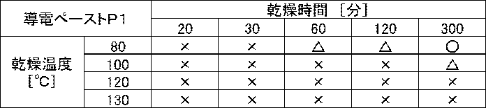


得られた導電ペ-ストP2~P4を用い、乾燥膜厚が17μmとなるように印刷し、乾燥温度と乾燥時間を変えて、リング状凹み欠点、細線両端導通性、細線両端間絶縁性を評価した。結果を表5~7に示す。



得られた導電ペ-ストP1~P4を用い、各々乾燥条件を変えてリング状凹み欠点が少なくなる条件を見つけ、細線両端間導通性、細線両端間絶縁性を評価した。結果を表8.に示す。

表11に示す配合比にて導電ペーストを調整した。まず、バインダ樹脂を固形分濃度が35質量%となるように溶剤適当量へ溶解し、得られたバインダー樹脂溶液、銀粉1、硬化剤、硬化触媒、残りの溶剤量、そのほか添加剤を秤量配合しプレミキシングの後、チルド三本ロール混練り機に2回通して分散した。次いで、ペースト濾過機(プロテック社製PF320A)に795メッシュ(ステンレスメッシュフィルター(線経16μm、目開き16μm)の濾過フィルターを取り付け、上記ペーストの濾過を行った。その後、得られた導電性ペーストを所定のパターンに印刷後、130℃×30分間乾燥し、導電性薄膜を得た。本導電性薄膜を用いて基本物性を測定し、次いで、レーザーエッチング加工の検討を行った。評価結果は、表11に示した。
導電性ペーストの樹脂および配合を変えて実施例12~21、比較例11~13を実施した。導電性ペーストの配合および評価結果を表11に示した。実施例においてはオーブン130℃×30分という比較的低温かつ短時間の加熱により良好な塗膜物性を得ることができた。またITO膜への密着性、湿熱環境試験後の評価も良好であった。

銀粉1:凝集銀粉(D50:1.3μm)
銀粉2:フレーク状銀粉(D50:1.3μm)
銀粉3:球状銀粉(D50:1.3μm)
バインダ樹脂1:InChem製PKHC(フェノキシ樹脂、数平均分子量21000、Tg=89℃)
バインダ樹脂2:InChme製PKHC変性物(フェノキシ樹脂、数平均分子量21000、Tg=97℃)
バインダ樹脂3:東洋紡製バイロン600(Tg=45℃、酸価30)
バインダ樹脂4:東洋紡製バイロン103(Tg=47℃、酸価25)
バインダ樹脂5:東洋紡製バイロン270(Tg=67℃、酸価30)
シリカ1:日本アロエジル製 AEROSIL 300 (一次粒子径:7nm)
シリカ2:日本アロエジル製 AEROSIL 130(一次粒子径:16nm)
シリカ3:日本アロエジル製 AEROSIL R972 (一次粒子径:16nm)
溶剤1:エチレングリコールモノブチルエーテルアセテート
溶剤2:ジエチレングリコールモノエチルエーテルアセテート
溶剤3:ジエチレングリコールモノブチルエーテルアセテート
硬化剤1:Baxenden製 ブロックイソシアネート BI7960
硬化剤1:Baxenden製 ブロックイソシアネート BI7982
硬化触媒:共同薬品(株)製KS1260
分散剤1:ビックケミー・ジャパン(株)社製Disperbyk167
添加剤1:カルボン酸アミン塩
添加剤2:カルボン酸
である。
表12に示す配合比にて導電ペーストを調整した。まず、バインダ樹脂を固形分濃度が35質量%となるように溶剤適当量へ溶解し、得られたバインダー樹脂溶液、銀粉1、硬化剤、硬化触媒、残りの溶剤量、そのほか添加剤を秤量配合しプレミキシングの後、チルド三本ロール混練り機に2回通して分散した。次いで、ペースト濾過機(プロテック社製PF320A)に795メッシュ(ステンレスメッシュフィルター(線経16μm、目開き16μm)の濾過フィルターを取り付け、上記ペーストの濾過を行った。その後、得られた導電性ペーストを所定のパターンに印刷後、130℃×30分間乾燥し、導電性薄膜を得た。本導電性薄膜を用いて基本物性を測定し、次いで、レーザーエッチング加工の検討を行った。評価結果は、表12に示した。
導電性ペーストの樹脂および配合を変えて実施例32~39、比較例31~33を実施した。導電性ペーストの配合および評価結果を表12に示した。実施例においてはオーブン130℃×30分という比較的低温かつ短時間の加熱により良好な塗膜物性を得ることができた。またITO膜への密着性、湿熱環境試験後の評価も良好であった。

銀粉1:凝集銀粉(D50:1.3μm)
銀粉2:フレーク状銀粉(D50:1.3μm)
銀粉3:球状銀粉(D50:1.3μm)
バインダ樹脂1:InChem製PKHC(フェノキシ樹脂、数平均分子量21000、Tg=89℃)
バインダ樹脂2:InChme製PKHC変性物(フェノキシ樹脂、数平均分子量21000、Tg=97℃)
バインダ樹脂3:東洋紡製バイロン600(Tg=45℃、酸価30)
バインダ樹脂4:東洋紡製バイロン103(Tg=47℃、酸価25)
バインダ樹脂5:東洋紡製バイロン270(Tg=67℃、酸価30)
カーボン1:ライオン製 ECP600JD (一次粒子径:34nm)
カーボン2:ライオン製 カーボンECP(一次粒子径:39.5nm)
カーボン3:東海カーボン製 トーカブラック♯5500 (算術平均粒子径:25nm)
カーボン4:東海カーボン製 トーかブラック♯4400 (算術平均粒子径:38nm)
溶剤1:エチレングリコールモノブチルエーテルアセテート
溶剤2:ジエチレングリコールモノエチルエーテルアセテート
溶剤3:ジエチレングリコールモノブチルエーテルアセテート
硬化剤1:Baxenden製 ブロックイソシアネート BI7960
硬化剤1:Baxenden製 ブロックイソシアネート BI7982
硬化触媒:共同薬品(株)製KS1260
分散剤1:ビックケミー・ジャパン(株)社製Disperbyk167
添加剤1:カルボン酸アミン塩
添加剤2:カルボン酸
である。
表13、表14に示す配合比にて導電ペーストを調整した。まず、バインダ樹脂を固形分濃度が35質量%となるように溶剤適当量へ溶解し、得られたバインダー樹脂溶液、銀粉1、硬化剤、硬化触媒、残りの溶剤量、そのほか添加剤を秤量配合しプレミキシングの後、チルド三本ロール混練り機に2回通して分散した。次いで、ペースト濾過機(プロテック社製PF320A)に795メッシュ(ステンレスメッシュフィルター(線経16μm、目開き16μm)の濾過フィルターを取り付け、上記ペーストの濾過を行った。その後、得られた導電性ペーストを所定のパターンに印刷後、130℃×30分間乾燥し、導電性薄膜を得た。本導電性薄膜を用いて基本物性を測定し、次いで、レーザーエッチング加工の検討を行った。評価結果は、表13、表14に示した。
導電性ペーストの樹脂および配合を変えて実施例42~57、比較例41~43を実施した。導電性ペーストの配合および評価結果を表13、表14に示した。実施例においてはオーブン130℃×30分という比較的低温かつ短時間の加熱により良好な塗膜物性を得ることができた。またITO膜への密着性、湿熱環境試験後の評価も良好であった。

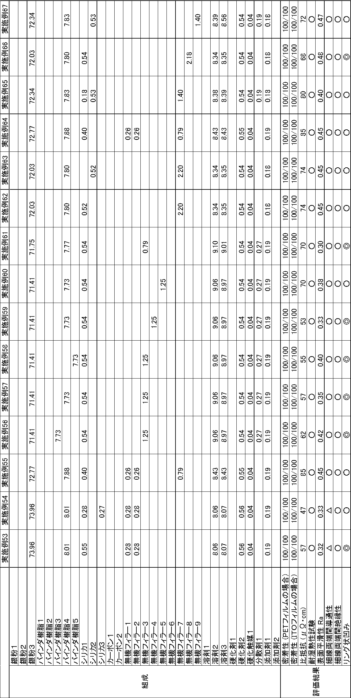
銀粉1:凝集銀粉(D50:1.3μm)
銀粉2:フレーク状銀粉(D50:1.3μm)
銀粉3:球状銀粉(D50:1.3μm)
バインダ樹脂1:InChem製PKHC(フェノキシ樹脂、数平均分子量21000、Tg=89℃)
バインダ樹脂2:InChme製PKHC変性物(フェノキシ樹脂、数平均分子量21000、Tg=97℃)
バインダ樹脂3:東洋紡製バイロン600(Tg=45℃、酸価30)
バインダ樹脂4:東洋紡製バイロン103(Tg=47℃、酸価25)
バインダ樹脂5:東洋紡製バイロン270(Tg=67℃、酸価30)
シリカ1:日本アロエジル製 AEROSIL 300 (一次粒子径:7nm)
シリカ2:日本アロエジル製 AEROSIL 130(一次粒子径:16nm)
シリカ3:日本アロエジル製 AEROSIL R972 (一次粒子径:16nm)
カーボン1:ライオン製 ECP600JD (一次粒子径:34nm)
カーボン2:ライオン製 カーボンECP(一次粒子径:39.5nm)
無機フィラー1:東亞合成製 イオン補足剤 IXE-700F (メジアン径:1.5μm)
無機フィラー2:東亞合成製 イオン補足剤IXE-100 (メジアン径:1.0μm)
無機フィラー3:東亞合成製 イオン補足剤IXE-PLAS A1 (メジアン径:0.5μm)
無機フィラー4:東亞合成製 イオン補足剤IXE-PLAS A2 (メジアン径:0.2μm)
無機フィラー5:東亞合成製 イオン補足剤IXE-PLAS B1 (メジアン径:0.4μm)
無機フィラー6:石原産業製 酸化チタンCR-57 (平均粒子径:0.25μm)
無機フィラー7:石原産業製 酸化チタンA-100 (平均粒子径:0.15μm)
無機フィラー8:堺化学製 硫酸バリウムB-1
無機フィラー9:堺化学製 硫酸バリウムB-65
溶剤1:エチレングリコールモノブチルエーテルアセテート
溶剤2:ジエチレングリコールモノエチルエーテルアセテート
溶剤3:ジエチレングリコールモノブチルエーテルアセテート
硬化剤1:Baxenden製 ブロックイソシアネート BI7960
硬化剤1:Baxenden製 ブロックイソシアネート BI7982
硬化触媒:共同薬品(株)製KS1260
分散剤1:ビックケミー・ジャパン(株)社製Disperbyk167
添加剤1:カルボン酸アミン塩
1b、2b、3b、4b : それぞれ細線1b、2b、3b、4b
1c、2c、3c、4c : それぞれ端子1c、2c、3c、4c
Claims (25)
- 導電フィラーとバインダ樹脂からなる導電性組成物により構成される導電性皮膜において、皮膜表面に存在する、直径50μm以下のリング状凹み欠点の存在密度が50個/cm2以下である事を特徴とする導電性皮膜。
- 前記導電性皮膜において、リング状凹みが存在しない部分の表面粗さRaが0.1以上、1.0μm以下であることを特徴とする請求項1記載の導電性皮膜。
- 前記導電性皮膜の平均膜厚が2μm以上、20μm以下であることを特徴とする請求項1または2記載の導電性皮膜。
- 前記導電性組成物が、少なくとも平均粒子径が0.3μm以上、6μm以下の銀粒子、および平均粒子径が5nm以上、200nm以下の二酸化珪素粒子、高分子バインダ樹脂を含有し、実質的に溶剤を含まないことを特徴とする請求項1から3のいずれかに記載の導電性皮膜。
- 前記導電性組成物が、少なくとも平均粒子径が0.3μm以上、6μm以下の銀粒子、および平均粒子径が5nm以上、200nm以下のカーボン粒子、高分子バインダ樹脂を含有し、実質的に溶剤を含まないことを特徴とする請求項1から3のいずれかに記載の導電性皮膜。
- 前記導電性組成物が、少なくとも平均粒子径が0.3μm以上、6μm以下の銀粒子、および平均粒子径が50nm以上、3000nm以下のイオン補足剤粒子、高分子バインダ樹脂を含有し、実質的に溶剤を含まないことを特徴とする請求項1から3のいずれかに記載の導電性皮膜。
- 励起光の光束により、請求項1から6のいずれかに記載の導電性皮膜の一部を除去するプロセスを有することを特徴とする電気配線の形成方法。
- 少なくとも高分子バインダ樹脂(A)、平均粒子径が0.3μm以上、6μm以下の金属粉(B)、有機溶剤(C)および平均粒子径が5nm以上、200nm以下の二酸化珪素粒子(D)を含有することを特徴とするレーザーエッチング加工用導電性ペースト。
- 前記バインダ樹脂(A)が、ポリエステル樹脂、ポリウレタン樹脂、エポキシ樹脂、フェノキシ樹脂、塩化ビニル樹脂、および繊維素誘導体樹脂からなる群から選ばれる1種又は2種以上の混合物であることを特徴とする請求項8記載のレーザーエッチング加工用導電性ペースト。
- 前記、バインダ樹脂(A)の数平均分子量が5,000~60,000、ガラス転移温度が120℃未満、であることを特徴とする請求項8または9に記載のレーザーエッチング加工用導電性ペースト。
- 前記有機溶剤(C)が、少なくとも沸点の異なる2種の溶剤の混合物であり、全溶剤量の45~90質量%を占める第1の溶剤の沸点が200℃以上、270℃以下であり、第2の溶剤の沸点は第一の溶剤の沸点より10℃以上低く、全溶剤量の55~10質量%であることを特徴とする請求項8から10のいずれかに記載のレーザーエッチング加工用導電性ペースト。
- 前記、バインダ樹脂(A)の酸価が400当量/106g未満であることを特徴とする請求項8から11のいずれかに記載のレーザーエッチング加工用導電性ペースト。
- 15μm以上の銀粗大粒子がペースト1.0gあたり、100個以下であることを特徴とする請求項8から12のいずれかに記載のレーザーエッチング加工用導電性ペースト。
- 少なくとも平均粒子径が0.3μm以上、6μm以下の金属粉(B)、および平均粒子径が5nm以上、200nm以下のカーボン粒子(E)、高分子バインダー樹脂(A)、有機溶剤(C)を含有することを特徴とするレーザーエッチング加工用導電性ペースト。
- 前記バインダ樹脂(A)が、ポリエステル樹脂、ポリウレタン樹脂、エポキシ樹脂、フェノキシ樹脂、塩化ビニル樹脂、および繊維素誘導体樹脂からなる群から選ばれる1種又は2種以上の混合物であることを特徴とする請求項14記載のレーザーエッチング加工用導電性ペースト。
- 前記、高分子バインダ樹脂(A)が、数平均分子量が5,000~60,000、ガラス転移温度が120℃未満、であることを特徴とする請求項14または15に記載のレーザーエッチング加工用導電性ペースト。
- 前記溶剤が、少なくとも沸点の異なる2種の溶剤の混合物であり、全溶剤量の45~90質量%を占める第1の溶剤の沸点が200℃以上、270℃以下であり、第2の溶剤の沸点は第一の溶剤の沸点より10℃以上低く、全溶剤量の55~10質量%であることを特徴とする請求項14から16のいずれかに記載のレーザーエッチング加工用導電性ペースト。
- 前記、高分子バインダ樹脂(A)の酸価が200当量/106g未満であることを特徴とする請求項14から17のいずれかに記載のレーザーエッチング加工用導電性ペースト。
- 15μm以上の銀粗大粒子がペースト1.0gあたり、100個以下であることを特徴とする請求項14から18のいずれかに記載のレーザーエッチング加工用導電性ペースト。
- 少なくとも
(B)平均粒子径が0.3μm以上、6μm以下の金属粒子、および
(G)平均粒子径が5nm以上、200nm以下のカーボンまたは二酸化珪素粒子、
(H)平均粒子径が0.1μm以上、3μm以下の無機粒子、
(A)高分子バインダー樹脂、
(E)溶剤
を含有することを特徴とするレーザーエッチング加工用導電性ペースト。 - 前記バインダ樹脂が、ポリエステル樹脂、ポリウレタン樹脂、エポキシ樹脂、フェノキシ樹脂、塩化ビニル樹脂、および繊維素誘導体樹脂からなる群から選ばれる1種又は2種以上の混合物であることを特徴とする請求項20記載のレーザーエッチング加工用導電性ペースト。
- 前記、高分子バインダ樹脂が、、数平均分子量が5,000~60,000、ガラス転移温度が120℃未満、であることを特徴とする請求項20または21に記載のレーザーエッチング加工用導電性ペースト。
- 前記溶剤が、少なくとも沸点の異なる2種の溶剤の混合物であり、全溶剤量の45~90質量%を占める第1の溶剤の沸点が200℃以上、270℃以下であり、第2の溶剤の沸点は第一の溶剤の沸点より10℃以上低く、全溶剤量の55~10質量%であることを特徴とする請求項20から22のいずれかに記載のレーザーエッチング加工用導電性ペースト。
- 前記、高分子バインダ樹脂の酸価が200当量/106g未満であることを特徴とする請求項20から23のいずれかに記載のレーザーエッチング加工用導電性ペースト。
- 15μm以上の銀粗大粒子がペースト1.0gあたり、100個以下であることを特徴とする請求項20から24のいずれかに記載のレーザーエッチング加工用導電性ペースト。
Priority Applications (3)
| Application Number | Priority Date | Filing Date | Title |
|---|---|---|---|
| KR1020187025703A KR102353074B1 (ko) | 2016-03-17 | 2017-03-02 | 도전성 피막 및 레이저 에칭 가공용 도전성 페이스트 |
| JP2018505804A JP7056552B2 (ja) | 2016-03-17 | 2017-03-02 | 導電性皮膜およびレーザーエッチング加工用導電性ペースト |
| CN201780016621.0A CN108781505B (zh) | 2016-03-17 | 2017-03-02 | 导电性覆膜以及激光蚀刻加工用导电性浆料 |
Applications Claiming Priority (8)
| Application Number | Priority Date | Filing Date | Title |
|---|---|---|---|
| JP2016053633 | 2016-03-17 | ||
| JP2016053632 | 2016-03-17 | ||
| JP2016053630 | 2016-03-17 | ||
| JP2016053631 | 2016-03-17 | ||
| JP2016-053631 | 2016-03-17 | ||
| JP2016-053633 | 2016-03-17 | ||
| JP2016-053632 | 2016-03-17 | ||
| JP2016-053630 | 2016-03-17 |
Publications (1)
| Publication Number | Publication Date |
|---|---|
| WO2017159381A1 true WO2017159381A1 (ja) | 2017-09-21 |
Family
ID=59851429
Family Applications (1)
| Application Number | Title | Priority Date | Filing Date |
|---|---|---|---|
| PCT/JP2017/008284 Ceased WO2017159381A1 (ja) | 2016-03-17 | 2017-03-02 | 導電性皮膜およびレーザーエッチング加工用導電性ペースト |
Country Status (5)
| Country | Link |
|---|---|
| JP (1) | JP7056552B2 (ja) |
| KR (1) | KR102353074B1 (ja) |
| CN (1) | CN108781505B (ja) |
| TW (1) | TWI710041B (ja) |
| WO (1) | WO2017159381A1 (ja) |
Cited By (2)
| Publication number | Priority date | Publication date | Assignee | Title |
|---|---|---|---|---|
| KR20200035886A (ko) * | 2018-09-27 | 2020-04-06 | 아지노모토 가부시키가이샤 | 수지 조성물, 감광성 필름, 지지체 부착 감광성 필름, 프린트 배선판 및 반도체 장치 |
| EP3648115A4 (en) * | 2017-06-30 | 2021-03-24 | Sekisui Chemical Co., Ltd. | CONDUCTIVE PASTE |
Families Citing this family (7)
| Publication number | Priority date | Publication date | Assignee | Title |
|---|---|---|---|---|
| CN112272966B (zh) * | 2018-06-20 | 2024-02-02 | 信越化学工业株式会社 | 转移装置、使用方法和调整方法 |
| CN109887638B (zh) * | 2019-01-14 | 2021-02-23 | 上海大学 | 纳米银颗粒与镀银碳化硅颗粒混合的多尺度纳米银浆及其制备方法 |
| US11056630B2 (en) | 2019-02-13 | 2021-07-06 | Samsung Electronics Co., Ltd. | Display module having glass substrate on which side wirings are formed and manufacturing method of the same |
| JP7393210B2 (ja) * | 2019-06-28 | 2023-12-06 | 株式会社Screenホールディングス | 基板処理方法および基板処理装置 |
| CN111243779A (zh) * | 2020-03-09 | 2020-06-05 | 广东四维新材料有限公司 | 用于激光切割导电银浆和低温固化超细球状银粉及彼此的制备方法 |
| CN113450943B (zh) * | 2021-09-02 | 2022-01-04 | 西安宏星电子浆料科技股份有限公司 | 一种抗热震型厚膜电路用导体浆料 |
| CN115910426A (zh) * | 2023-01-06 | 2023-04-04 | 北京中科纳通电子技术有限公司 | 一种高触变性的导电银浆及其制备方法 |
Citations (4)
| Publication number | Priority date | Publication date | Assignee | Title |
|---|---|---|---|---|
| JP2005353783A (ja) * | 2004-06-10 | 2005-12-22 | Mitsubishi Plastics Ind Ltd | 多層配線基板用導電性ペースト組成物 |
| JP2008013809A (ja) * | 2006-07-05 | 2008-01-24 | Az Electronic Materials Kk | レーザーアブレーションによる機能膜の製造法およびそれに用いるレーザーアブレーション加工用組成物 |
| JP2015115314A (ja) * | 2013-12-12 | 2015-06-22 | ペルノックス株式会社 | レーザーエッチング用導電性銀ペースト、回路基板用基材および回路基板 |
| WO2015111615A1 (ja) * | 2014-01-22 | 2015-07-30 | 東洋紡株式会社 | レーザーエッチング加工用導電性ペースト、導電性薄膜、導電性積層体 |
Family Cites Families (11)
| Publication number | Priority date | Publication date | Assignee | Title |
|---|---|---|---|---|
| JP5236557B2 (ja) | 2009-03-31 | 2013-07-17 | 太陽ホールディングス株式会社 | レーザーを用いたパターン形成方法 |
| JP2011181338A (ja) | 2010-03-01 | 2011-09-15 | Taiyo Holdings Co Ltd | レーザーを用いた導電パターン形成方法及びその方法に用いる組成物 |
| JP6016328B2 (ja) | 2011-02-07 | 2016-10-26 | 株式会社三共 | 遊技用システム |
| MX2013013609A (es) * | 2011-05-23 | 2014-01-08 | Nissan Motor | Pelicula conductiva, colector de corriente que usa la misma, bateria y bateria bipolar. |
| CN103875042A (zh) * | 2011-11-30 | 2014-06-18 | 东洋纺株式会社 | 透明导电性薄膜 |
| WO2013146483A1 (ja) * | 2012-03-30 | 2013-10-03 | 帝人株式会社 | 透明導電性積層体 |
| JP6079425B2 (ja) * | 2012-05-16 | 2017-02-15 | 日立化成株式会社 | 導電粒子、異方性導電接着剤フィルム及び接続構造体 |
| JP2014002992A (ja) | 2012-06-14 | 2014-01-09 | Pelnox Ltd | レーザーエッチング用導電性ペースト組成物 |
| JP6227321B2 (ja) * | 2013-08-05 | 2017-11-08 | リンテック株式会社 | プロテクトフィルム付き透明導電性フィルム |
| JP2015050107A (ja) * | 2013-09-03 | 2015-03-16 | 富士フイルム株式会社 | 導電膜の製造方法 |
| JP5932098B2 (ja) * | 2014-04-17 | 2016-06-08 | 日東電工株式会社 | 透明導電性フィルム |
-
2017
- 2017-03-02 KR KR1020187025703A patent/KR102353074B1/ko active Active
- 2017-03-02 JP JP2018505804A patent/JP7056552B2/ja active Active
- 2017-03-02 WO PCT/JP2017/008284 patent/WO2017159381A1/ja not_active Ceased
- 2017-03-02 CN CN201780016621.0A patent/CN108781505B/zh active Active
- 2017-03-07 TW TW106107299A patent/TWI710041B/zh active
Patent Citations (4)
| Publication number | Priority date | Publication date | Assignee | Title |
|---|---|---|---|---|
| JP2005353783A (ja) * | 2004-06-10 | 2005-12-22 | Mitsubishi Plastics Ind Ltd | 多層配線基板用導電性ペースト組成物 |
| JP2008013809A (ja) * | 2006-07-05 | 2008-01-24 | Az Electronic Materials Kk | レーザーアブレーションによる機能膜の製造法およびそれに用いるレーザーアブレーション加工用組成物 |
| JP2015115314A (ja) * | 2013-12-12 | 2015-06-22 | ペルノックス株式会社 | レーザーエッチング用導電性銀ペースト、回路基板用基材および回路基板 |
| WO2015111615A1 (ja) * | 2014-01-22 | 2015-07-30 | 東洋紡株式会社 | レーザーエッチング加工用導電性ペースト、導電性薄膜、導電性積層体 |
Cited By (5)
| Publication number | Priority date | Publication date | Assignee | Title |
|---|---|---|---|---|
| EP3648115A4 (en) * | 2017-06-30 | 2021-03-24 | Sekisui Chemical Co., Ltd. | CONDUCTIVE PASTE |
| US10984921B2 (en) | 2017-06-30 | 2021-04-20 | Sekisui Chemical Co., Ltd. | Conductive paste |
| KR20200035886A (ko) * | 2018-09-27 | 2020-04-06 | 아지노모토 가부시키가이샤 | 수지 조성물, 감광성 필름, 지지체 부착 감광성 필름, 프린트 배선판 및 반도체 장치 |
| JP7281263B2 (ja) | 2018-09-27 | 2023-05-25 | 味の素株式会社 | 樹脂組成物、感光性フィルム、支持体付き感光性フィルム、プリント配線板及び半導体装置 |
| KR102807956B1 (ko) * | 2018-09-27 | 2025-05-19 | 아지노모토 가부시키가이샤 | 수지 조성물, 감광성 필름, 지지체 부착 감광성 필름, 프린트 배선판 및 반도체 장치 |
Also Published As
| Publication number | Publication date |
|---|---|
| CN108781505A (zh) | 2018-11-09 |
| TWI710041B (zh) | 2020-11-11 |
| CN108781505B (zh) | 2021-08-06 |
| JP7056552B2 (ja) | 2022-04-19 |
| TW201735219A (zh) | 2017-10-01 |
| JPWO2017159381A1 (ja) | 2019-01-24 |
| KR20180121522A (ko) | 2018-11-07 |
| KR102353074B1 (ko) | 2022-01-19 |
Similar Documents
| Publication | Publication Date | Title |
|---|---|---|
| JP7059240B2 (ja) | レーザーエッチング加工用導電性ペースト、導電性薄膜および導電性積層体 | |
| JP7056552B2 (ja) | 導電性皮膜およびレーザーエッチング加工用導電性ペースト | |
| CN106415735B (zh) | 激光蚀刻加工用导电浆料、导电性薄膜、导电性层叠体 | |
| JP6582982B2 (ja) | レーザーエッチング加工用導電性ペースト、導電性薄膜、導電性積層体 | |
| JP6673215B2 (ja) | レーザーエッチング加工用導電性ペースト、導電性薄膜、導電性積層体 |
Legal Events
| Date | Code | Title | Description |
|---|---|---|---|
| WWE | Wipo information: entry into national phase |
Ref document number: 2018505804 Country of ref document: JP |
|
| ENP | Entry into the national phase |
Ref document number: 20187025703 Country of ref document: KR Kind code of ref document: A |
|
| NENP | Non-entry into the national phase |
Ref country code: DE |
|
| 121 | Ep: the epo has been informed by wipo that ep was designated in this application |
Ref document number: 17766384 Country of ref document: EP Kind code of ref document: A1 |
|
| 122 | Ep: pct application non-entry in european phase |
Ref document number: 17766384 Country of ref document: EP Kind code of ref document: A1 |