WO2017159118A1 - 光導波路 - Google Patents
光導波路 Download PDFInfo
- Publication number
- WO2017159118A1 WO2017159118A1 PCT/JP2017/004288 JP2017004288W WO2017159118A1 WO 2017159118 A1 WO2017159118 A1 WO 2017159118A1 JP 2017004288 W JP2017004288 W JP 2017004288W WO 2017159118 A1 WO2017159118 A1 WO 2017159118A1
- Authority
- WO
- WIPO (PCT)
- Prior art keywords
- core
- light
- optical waveguide
- absorbing portion
- light absorbing
- Prior art date
Links
Images


Classifications
-
- G—PHYSICS
- G02—OPTICS
- G02B—OPTICAL ELEMENTS, SYSTEMS OR APPARATUS
- G02B6/00—Light guides; Structural details of arrangements comprising light guides and other optical elements, e.g. couplings
- G02B6/10—Light guides; Structural details of arrangements comprising light guides and other optical elements, e.g. couplings of the optical waveguide type
- G02B6/12—Light guides; Structural details of arrangements comprising light guides and other optical elements, e.g. couplings of the optical waveguide type of the integrated circuit kind
- G02B6/122—Basic optical elements, e.g. light-guiding paths
-
- G—PHYSICS
- G02—OPTICS
- G02F—OPTICAL DEVICES OR ARRANGEMENTS FOR THE CONTROL OF LIGHT BY MODIFICATION OF THE OPTICAL PROPERTIES OF THE MEDIA OF THE ELEMENTS INVOLVED THEREIN; NON-LINEAR OPTICS; FREQUENCY-CHANGING OF LIGHT; OPTICAL LOGIC ELEMENTS; OPTICAL ANALOGUE/DIGITAL CONVERTERS
- G02F1/00—Devices or arrangements for the control of the intensity, colour, phase, polarisation or direction of light arriving from an independent light source, e.g. switching, gating or modulating; Non-linear optics
- G02F1/01—Devices or arrangements for the control of the intensity, colour, phase, polarisation or direction of light arriving from an independent light source, e.g. switching, gating or modulating; Non-linear optics for the control of the intensity, phase, polarisation or colour
- G02F1/21—Devices or arrangements for the control of the intensity, colour, phase, polarisation or direction of light arriving from an independent light source, e.g. switching, gating or modulating; Non-linear optics for the control of the intensity, phase, polarisation or colour by interference
- G02F1/225—Devices or arrangements for the control of the intensity, colour, phase, polarisation or direction of light arriving from an independent light source, e.g. switching, gating or modulating; Non-linear optics for the control of the intensity, phase, polarisation or colour by interference in an optical waveguide structure
-
- G—PHYSICS
- G02—OPTICS
- G02B—OPTICAL ELEMENTS, SYSTEMS OR APPARATUS
- G02B6/00—Light guides; Structural details of arrangements comprising light guides and other optical elements, e.g. couplings
- G02B6/10—Light guides; Structural details of arrangements comprising light guides and other optical elements, e.g. couplings of the optical waveguide type
- G02B6/12—Light guides; Structural details of arrangements comprising light guides and other optical elements, e.g. couplings of the optical waveguide type of the integrated circuit kind
- G02B2006/12083—Constructional arrangements
- G02B2006/12097—Ridge, rib or the like
-
- G—PHYSICS
- G02—OPTICS
- G02B—OPTICAL ELEMENTS, SYSTEMS OR APPARATUS
- G02B6/00—Light guides; Structural details of arrangements comprising light guides and other optical elements, e.g. couplings
- G02B6/10—Light guides; Structural details of arrangements comprising light guides and other optical elements, e.g. couplings of the optical waveguide type
- G02B6/12—Light guides; Structural details of arrangements comprising light guides and other optical elements, e.g. couplings of the optical waveguide type of the integrated circuit kind
- G02B2006/12083—Constructional arrangements
- G02B2006/12126—Light absorber
-
- G—PHYSICS
- G02—OPTICS
- G02B—OPTICAL ELEMENTS, SYSTEMS OR APPARATUS
- G02B6/00—Light guides; Structural details of arrangements comprising light guides and other optical elements, e.g. couplings
- G02B6/10—Light guides; Structural details of arrangements comprising light guides and other optical elements, e.g. couplings of the optical waveguide type
- G02B6/12—Light guides; Structural details of arrangements comprising light guides and other optical elements, e.g. couplings of the optical waveguide type of the integrated circuit kind
- G02B6/122—Basic optical elements, e.g. light-guiding paths
- G02B6/125—Bends, branchings or intersections
-
- G—PHYSICS
- G02—OPTICS
- G02B—OPTICAL ELEMENTS, SYSTEMS OR APPARATUS
- G02B6/00—Light guides; Structural details of arrangements comprising light guides and other optical elements, e.g. couplings
- G02B6/10—Light guides; Structural details of arrangements comprising light guides and other optical elements, e.g. couplings of the optical waveguide type
- G02B6/12—Light guides; Structural details of arrangements comprising light guides and other optical elements, e.g. couplings of the optical waveguide type of the integrated circuit kind
- G02B6/13—Integrated optical circuits characterised by the manufacturing method
- G02B6/132—Integrated optical circuits characterised by the manufacturing method by deposition of thin films
-
- G—PHYSICS
- G02—OPTICS
- G02B—OPTICAL ELEMENTS, SYSTEMS OR APPARATUS
- G02B6/00—Light guides; Structural details of arrangements comprising light guides and other optical elements, e.g. couplings
- G02B6/10—Light guides; Structural details of arrangements comprising light guides and other optical elements, e.g. couplings of the optical waveguide type
- G02B6/12—Light guides; Structural details of arrangements comprising light guides and other optical elements, e.g. couplings of the optical waveguide type of the integrated circuit kind
- G02B6/13—Integrated optical circuits characterised by the manufacturing method
- G02B6/136—Integrated optical circuits characterised by the manufacturing method by etching
Definitions
- the present invention relates to an optical waveguide used in the fields of optical communication, optical information processing, and other general optics.
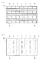
- the optical waveguide W13 is generally provided on the surface of the underclad 1 for light propagation as shown in a plan view in FIG. 13 (a) and in a cross-sectional view taken along a line CC in FIG. 13 (a).
- a linear core 2 is projected in a predetermined pattern, and an overclad 3 is formed in a state of covering the core 2.
- the optical waveguide W13 allows light to enter from the light incident portion 2a at the first end of the core 2 and emits the light from the light emitting portion 2b at the second end of the core 2.
- reference numeral 5 denotes a substrate used when manufacturing the optical waveguide W13.
- foreign matter may be mixed into the core 2 or the interface may be formed on a rough surface. If foreign matter is mixed in the core 2, when the light propagating through the core 2 hits the foreign matter, it reflects in an abnormal direction, does not reflect at the interface, and passes through the interface (core 2 (see an arrow L1 indicated by a two-dot chain line). Further, when the interface is formed on a rough surface, the light reaching the interface may not be reflected by the interface and may pass through the interface (leak from the core 2) (arrow indicated by a two-dot chain line) L2).
- the optical waveguide W ⁇ b> 13 in which a plurality of light propagation cores 2 are formed in parallel when light leaks from the core 2 as described above, the leaked light is mixed into the adjacent core 2.
- Cross talk "occurs.
- the light mixed in the adjacent core 2 is noise (N) for the light (signal S) propagating through the adjacent core 2 and deteriorates the S / N ratio and makes optical communication unstable.
- FIG. 14A a plan view in FIG. 14A and in a DD cross-sectional view in FIG. 14B, between adjacent cores 2 for light propagation, as shown in FIG.
- a dummy core 20 that is not used for light propagation is provided using the same forming material as that of the core 2, and an optical waveguide W14 in which crosstalk is suppressed by the dummy core 20 has been proposed (see, for example, Patent Document 1).
- the refractive index of the dummy core 20 is larger than the refractive indexes of the underclad 1 and the overclad 3 as in the case of the core 2. The light is less likely to leak from the dummy core 20.
- the core 2 and the dummy core 20 are hatched with broken lines, and the interval between the hatched lines is greater for the dummy core 20 than for the core 2. It is also wide.
- the present invention has been made in view of such circumstances, and provides an optical waveguide capable of improving the suppression of crosstalk.
- An optical waveguide of the present invention is an optical waveguide comprising a plurality of light propagation cores arranged in parallel and a light absorbing portion provided in a non-contact state with the cores adjacent to each other.
- the light absorption part includes a light absorber having an ability to absorb light propagating through the core.
- the present inventors have studied the structure of the optical waveguide in order to improve the suppression of crosstalk between the cores in the optical waveguide in which a plurality of cores for light propagation are arranged in parallel.
- the light absorption part contains the light absorber which has the absorptivity of the light which propagates in the said core.
- the light absorption part when the light absorption part is provided in contact with the core, it has been found that light propagating in the core is absorbed and attenuated by the light absorption part every time it is reflected at the interface with the light absorption part. That is, if the light absorbing portion is in contact with the core, even if the suppression of crosstalk can be improved, the light propagation in the core is not properly performed. Thus, it has been found that as a result of providing the light absorbing portion in a non-contact state with the core, the suppression of crosstalk can be improved and the light propagation in the core is also made appropriate.
- the optical waveguide of the present invention has a plurality of light propagation cores arranged in parallel, and a light absorbing portion is provided between adjacent cores.
- the light absorption part contains the light absorber which has the absorptivity of the light which propagates in the said core.
- the optical waveguide of the present invention has an effect of suppressing crosstalk.
- the optical waveguide of the present invention is provided with the light absorbing portion in a non-contact state with the core. Therefore, the light propagating in the core can be propagated in the core without being absorbed and attenuated by the light absorbing portion.
- the clad is generally used for an optical waveguide, so that a large cost is required. Therefore, suppression of crosstalk can be improved.
- the non-contact state between the core and the light absorbing portion can be more reliably maintained. Therefore, attenuation of light propagating through the core can be prevented more reliably.
- the light absorbing portion ensures that light (disturbance light) from the outside of the optical waveguide of the present invention is mixed into the core. Can be prevented.
- the difference in refractive index between the core and air (air cladding) becomes larger, so that light propagating in the core is less likely to leak from the core, and crosstalk. Can be further improved.
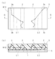
- optical waveguide of the 1st Embodiment of this invention is shown typically, (a) is the top view of the optical waveguide, (b) is AA sectional drawing of (a).
- (A)-(d) is explanatory drawing which shows typically the manufacturing method of the said optical waveguide. It is sectional drawing which shows typically the optical waveguide of the 2nd Embodiment of this invention. It is sectional drawing which shows typically the optical waveguide of the 3rd Embodiment of this invention. It is sectional drawing which shows typically the optical waveguide of the 4th Embodiment of this invention. It is sectional drawing which shows typically the optical waveguide of the 5th Embodiment of this invention.
- FIG. 1 It is sectional drawing which shows typically the optical waveguide of the 6th Embodiment of this invention.
- the optical waveguide of the 7th Embodiment of this invention is shown typically, (a) is a top view of the optical waveguide, (b) is BB sectional drawing of (a).
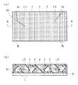
- FIG. A conventional optical waveguide is schematically shown, in which (a) is a plan view of the optical waveguide, and (b) is a cross-sectional view taken along the line CC of (a).
- Another conventional optical waveguide is schematically shown, in which (a) is a plan view of the optical waveguide, and (b) is a DD cross-sectional view of (a).
- FIG. 1A is a plan view showing an optical waveguide W1 according to the first embodiment of the present invention
- FIG. 1B is a cross-sectional view taken along line AA in FIG.
- the optical waveguide W1 of the first embodiment includes a plurality of (in the figure, four) strip-like underclad 1 arranged in parallel, and one on each surface of the underclad 1 along the longitudinal direction of the underclad 1.
- a light absorbing portion 4 formed integrally with the side surface and the side surface and top surface of the over clad 3.
- the light absorbing portion 4 contains a light absorber having an ability to absorb light propagating through the core 2.
- the first end portion of each core 2 in the longitudinal direction is a light incident portion 2a
- the second end portion is a light emitting portion 2b, and incident from the light incident portion 2a.
- the transmitted light passes through the core 2 and propagates to the light emitting portion 2b.
- FIG. 1A in order to clarify the arrangement of the core 2 and the light absorbing portion 4 which are main components, a part of the configuration of the over clad 3 and the like is omitted.
- reference numeral 5 denotes a substrate used when the optical waveguide W1 is manufactured.
- the light hits the light absorbing portion 4 and is absorbed, It does not mix in the adjacent core 2 (see L5 and L6 indicated by a two-dot chain line). Therefore, suppression of crosstalk can be improved.
- the light absorbing portion 4 is provided between the adjacent core 2 and the core 2 via the overcladding 3 and is in a non-contact state with the core 2. Is absorbed by the light absorbing portion 4 and is not attenuated, and proper light propagation is performed.
- the light absorber 4 will be described in more detail.
- the light absorber include diimonium salts, cyanine dyes, naphthalocyanine dyes, phthalocyanine dyes, and the like.
- the light absorber contained in the light absorber 4 is determined by the wavelength of light to be absorbed (that is, the wavelength of light propagating through the core 2), and the light absorber exemplified above has a wavelength in the range of 750 to 1000 nm. It is suitable for light absorption.
- the material for forming the light absorbing portion 4 include a photocurable resin and a thermosetting resin.
- the content of the light absorbent is, for example, 0.3 to 2.0 for the photocurable resin. % By weight, and 0.5 to 30.0% by weight for thermosetting resins.
- the said light absorber is used individually or in combination of 2 or more types.
- a substrate 5 (see FIG. 2A) is prepared.
- the material for forming the substrate 5 include metal, resin, glass, quartz, and silicon.
- the thickness of the substrate 5 is set within a range of 10 to 1000 ⁇ m, for example.
- a plurality of parallel strip-like under clads 1 are formed on the surface of the substrate 5 by photolithography using a photosensitive resin that is a material for forming the under clad 1.
- the dimensions of the underclad 1 are set, for example, in the range of 5 to 50 ⁇ m in thickness, in the range of 30 to 500 ⁇ m, and the width of the gap between adjacent underclad 1 and underclad 1 is 20 ⁇ m. Set as above.
- a photosensitive resin that is a material for forming the core 2 is used on the surface of each underclad 1, and along the longitudinal direction of the underclad 1 by photolithography, One core 2 is formed at a time.
- the dimensions of the core 2 are set, for example, in the range of 10 to 80 ⁇ m in thickness, and the width is set in the range of 8 to 90% of the width of the undercladding 1.
- the width T1 of the gap is set within the range of 20 to 500 ⁇ m.
- a photosensitive resin having a refractive index higher than that of the material for forming the under cladding 1 and the following over cladding 3 is used.
- a photosensitive resin which is a material for forming the overclad 3 is used on the surface of each underclad 1, and along the side and top surfaces of each core 2 by photolithography. Then, the over clad 3 is formed with the core 2 covered.
- the thickness of the over clad 3 is set, for example, in the range of 3 to 500 ⁇ m for the portion covering the side surface of the core 2 and in the range of 3 to 50 ⁇ m for the portion covering the top surface of the core 2.
- the light absorbing portion 4 is formed integrally with the surface of the substrate 5 covered with the side surface of the underclad 1 and the side surface and top surface of the overclad 3. .
- the light absorbing portion 4 is formed by a manufacturing method corresponding to the material for forming the light absorbing portion 4 (photocurable resin, thermosetting resin, etc.).
- the dimension of the light absorbing portion 4 is set such that, for example, the thickness T2 from the top surface of the overclad 3 exceeds 0 (zero) and is 200 ⁇ m or less, and is sandwiched between adjacent overclad 3 and overclad 3.
- the width T3 of the existing portion exceeds 0 (zero) and is set to 400 ⁇ m or less, preferably in the range of 10 to 250 ⁇ m.
- the optical waveguide W1 composed of the under cladding 1, the core 2, the over cladding 3, and the light absorbing portion 4 can be produced on the surface of the substrate 5.
- the optical waveguide W1 may be used in contact with the surface of the substrate 5 or may be used after being peeled from the substrate 5.
- FIG. 3 is a cross-sectional view (a cross-sectional view corresponding to FIG. 1B) showing an optical waveguide W2 according to a second embodiment of the present invention.
- a layer of the light absorbing portion 4 is also provided between the underclad 1 and the substrate 5. It has become a thing. That is, a single layer of the light absorbing portion 4 is formed on the surface of the substrate 5, and the under cladding 1 is formed on the surface of the layer of the light absorbing portion 4.
- the layer of the light absorbing portion 4 is also a part of the configuration of the optical waveguide W2.
- Other parts are the same as those in the first embodiment shown in FIGS. 1A and 1B, and the same reference numerals are given to the same parts.
- FIG. 4 is a cross-sectional view (a cross-sectional view corresponding to FIG. 1B) showing an optical waveguide W3 according to a third embodiment of the present invention.
- the substrate 5 is formed of the material for forming the light absorbing portion 4 in the first embodiment shown in FIGS. 1 (a) and 1 (b).
- the optical waveguide W3 is used in contact with the surface of the substrate 5.
- Other parts are the same as those in the first embodiment shown in FIGS. 1A and 1B, and the same reference numerals are given to the same parts.
- the substrate 5 in addition to the light absorption effect by the light absorbing portion 4 as in the first embodiment, the substrate 5 also absorbs light leaking from the bottom surface of the underclad 1. Can do. Therefore, the suppression of crosstalk can be further improved.
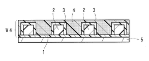
- FIG. 5 is a cross-sectional view (a cross-sectional view corresponding to FIG. 1B) showing an optical waveguide W4 according to a fourth embodiment of the present invention.
- the undercladding 1 is not formed as a plurality of parallel strips in the first embodiment shown in FIGS. 1A and 1B but as an integral layer. It is in a formed state.
- the light absorbing portion 4 is formed on the surface portion of the under cladding 1 except for the core 2 and the over cladding 3.
- Other parts are the same as those in the first embodiment shown in FIGS. 1A and 1B, and the same reference numerals are given to the same parts.
- the light leaking from the core 2 further leaks from the side surface and the top surface of the over clad 3, the light hits the light absorbing portion 4 and is absorbed. Therefore, suppression of crosstalk can be improved.
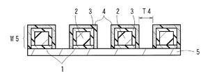
- FIG. 6 is a cross-sectional view (a cross-sectional view corresponding to FIG. 1B) showing an optical waveguide W5 according to a fifth embodiment of the present invention.
- the light absorbing portion 4 is made to correspond to the core 2 and independent from each other. Yes. That is, a gap is provided between the adjacent light absorbing portions 4 and the light absorbing portions 4 so that each light absorbing portion 4 covers the side surface of each under cladding 1 and the side surface and top surface of each over cladding 3. It has become.
- the optical waveguide W5 is used in contact with the surface of the substrate 5.
- Other parts are the same as those in the first embodiment shown in FIGS. 1A and 1B, and the same reference numerals are given to the same parts.
- the light absorption effect by the light absorption unit 4 is obtained as in the first embodiment. Further, the side surface and the top surface of each light absorbing portion 4 are in contact with air, and the refractive index of the light absorbing portion 4 is usually larger than the refractive index of air. Light is difficult to leak from the light absorbing portion 4 to the outside air. Therefore, the suppression of crosstalk can be further improved.
- the gap between the adjacent light absorbing portions 4 and the light absorbing portions 4 is formed by patterning the light absorbing portions 4 by a photolithography method in the step of forming the light absorbing portions 4 (see FIG. 2D). Made. Or you may form the said clearance gap by cutting the light absorption part 4 of the optical waveguide W1 of the said 1st Embodiment shown to Fig.1 (a), (b).
- the width T4 of the gap need only exceed 0 (zero), and is preferably in the range of 5 to 200 ⁇ m.
- FIG. 7 is a cross-sectional view (a cross-sectional view corresponding to FIG. 1B) showing an optical waveguide W6 according to a sixth embodiment of the present invention.
- the sixth embodiment is the same as the first embodiment shown in FIGS. 1A and 1B in that the thickness of the light absorbing portion 4 is reduced so that the light absorbing portion 4 is It is formed without covering the top surface.
- the height position of the surface of the said light absorption part 4 is set higher than the height position of the bottom face of the core 2 (the height position of the surface of the under clad 1).
- Other parts are the same as those in the first embodiment shown in FIGS. 1A and 1B, and the same reference numerals are given to the same parts.
- setting the height position of the surface of the light absorbing portion 4 to the height position of the top surface of the core 2 further improves the suppression of crosstalk. It is preferable from the viewpoint that can be made. Note that the height position of the surface of the light absorbing portion 4 may be set higher than the height position of the top surface of the core 2.
- the height position of the surface of the light absorbing portion 4 may be set in the same manner as in the sixth embodiment.
- FIG. 8A is a plan view showing an optical waveguide W7 according to a seventh embodiment of the present invention
- FIG. 8B is a cross-sectional view taken along the line BB of FIG. 8A.
- the optical waveguide W7 of the seventh embodiment includes a single undercladding layer 1 and a plurality of (four in the figure) linear cores 2 formed in parallel at a predetermined position on the surface of the undercladding 1.
- a linear light absorbing portion 4 formed in parallel with the core 2 in a non-contact state with the core 2 on the surface portion of the underclad 1 between the adjacent cores 2 and 2,
- An overclad 3 formed on the surface of the underclad 1 in a state of covering the core 2 and the light absorbing part 4 is provided.
- the said core 2 and the said light absorption part 4 are formed in the same thickness.
- Other parts are the same as those in the first embodiment shown in FIGS. 1A and 1B, and the same reference numerals are given to the same parts.
- FIG. 8A the core 2 is hatched with a broken line in order to clarify the arrangement of the core 2 and the light absorbing portion 4 which are main components.
- the seventh embodiment even if the light leaking from the core 2 is directed to the adjacent core 2, the light hits the light absorbing portion 4 and is absorbed. Therefore, suppression of crosstalk can be improved.
- the light absorbing portion 4 can be formed with a smaller volume than in the first to sixth embodiments, and the material for forming the light absorbing portion 4 can be saved. can do.
- the underclad 1 is formed on the surface of the substrate 5.
- the core 2 is formed on the surface of the underclad 1.
- a light absorbing portion 4 is formed on the surface of the under cladding 1 with a gap from the core 2.
- an over clad 3 is formed on the surface of the under clad 1 in a state where the core 2 and the light absorbing portion 4 are covered.
- the order of forming the core 2 and the light absorbing portion 4 may be reversed.
- the width T5 of the light absorbing portion 4 only needs to exceed 0 (zero), and is preferably in the range of 10 to 250 ⁇ m.
- the width T6 of the gap between the adjacent core 2 and the light absorbing portion 4 only needs to exceed 0 (zero), and is preferably in the range of 5 to 200 ⁇ m.
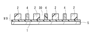
- FIG. 9 is a cross-sectional view (a cross-sectional view corresponding to FIG. 8B) showing an optical waveguide W8 according to an eighth embodiment of the present invention.
- the over clad 3 is made to correspond to the core 2 and independent from each other. . That is, each core 2 is covered with one overclad 3 and the light absorbing portion 4 is not covered with the overclad 3.
- a gap is provided between the adjacent overclad 3 and the light absorbing portion 4.
- the other parts are the same as those in the seventh embodiment shown in FIGS. 8A and 8B, and the same reference numerals are given to the same parts.
- the light absorption effect by the light absorption unit 4 is obtained as in the seventh embodiment. Further, the side surface and the top surface of each overclad 3 are in contact with air, and the refractive index of the overclad 3 is larger than the refractive index of air. It is difficult for air to leak from the cladding 3 to the outside air. Therefore, the suppression of crosstalk can be further improved.
- the formation of the gap between the adjacent overclad 3 and the light absorbing portion 4 is performed by using the overcladding 3 in the manufacturing method of the optical waveguide W7 of the seventh embodiment shown in FIGS. 8A and 8B. This is done by forming a pattern by lithography.
- the width T7 of the gap needs only to exceed 0 (zero), and is preferably in the range of 5 to 200 ⁇ m.
- the thickness of the light absorbing portion 4 is the same as the thickness of the core 2, but the thickness of the light absorbing portion 4 only needs to exceed 0 (zero).
- the upper limit of the thickness of the light absorbing portion 4 may be less than the thickness of the core 2 or may exceed the thickness of the core 2.
- the overcladding 3 made of resin is formed.
- the over clad 3 may not be formed. That is, instead of the overclad 3 made of resin, a clad (air clad) 30 made of air may be used. In this way, since the difference in refractive index between the core 2 and air (air clad 30) becomes larger, light propagating through the core 2 is less likely to leak from the core 2, and the suppression of crosstalk is further improved. be able to.
- the linear light absorbing portion 4 has a uniform width in the longitudinal direction [see FIG. 8A], but it does not have to be a uniform width.
- the width of the central portion in the longitudinal direction of the light absorbing portion 4 may be intermittently increased, or the width is gradually increased toward the center in the longitudinal direction. It may be wide (not shown). Conversely, the width of both end portions in the longitudinal direction of the light absorbing portion 4 may be increased.
- FIG. 11 the modification of 7th Embodiment [refer Fig.8 (a)] is shown in figure.
- the light absorbing portion 4 is continuously formed from one end to the other end in the longitudinal direction of the optical waveguides W1 to W10.
- FIG. You may form intermittently like the optical waveguides W11 and W12 shown with a top view in b).
- FIG. 12A shows a modification of the first embodiment [see FIG. 1A]
- FIG. 12B shows the seventh embodiment [see FIG. 8A]. ] Is illustrated.
- Component a 70 g of epoxy resin (manufactured by Mitsubishi Chemical Corporation, jER1001).
- Component b 20 g of epoxy resin (manufactured by Daicel, EHPE3150).
- Component c 10 g of epoxy resin (manufactured by DIC, EXA-4816).
- Component d 0.5 g of a photoacid generator (manufactured by Sun Apro, CPI-101A).
- Ingredient e 0.5 g of antioxidant (Kyodo Pharmaceutical Co., Ltd., Songnox 1010).
- Component f 0.5 g of antioxidant (manufactured by Sanko Co., Ltd., HCA).
- Component g 50 g of ethyl lactate (solvent).
- Component h 50 g of epoxy resin (manufactured by Nippon Steel Chemical Co., Ltd., YDCN-700-3).
- Component i 30 g of epoxy resin (manufactured by Mitsubishi Chemical Corporation, jER1002).
- Component j 20 g of an epoxy resin (Ogsol PG-100, manufactured by Osaka Gas Chemical Company).
- Component k 0.5 g of a photoacid generator (manufactured by Sun Apro, CPI-101A).
- Ingredient l 0.5 g of antioxidant (manufactured by Kyodo Pharmaceutical Co., Ltd., Songnox 1010).
- Component m 0.125 g of antioxidant (manufactured by Sanko Co., Ltd., HCA).
- Component n 50 g of ethyl lactate (solvent).
- a core forming material was prepared by mixing these components h to n.
- [Material for forming light absorbing portion] Component o: 50 g of epoxy resin (manufactured by Nippon Steel Chemical Co., Ltd., YDCN-700-3). Component p: 30 g of epoxy resin (manufactured by Mitsubishi Chemical Corporation, jER1002). Component q: 20 g of epoxy resin (Ogsol PG-100, manufactured by Osaka Gas Chemical Company). Component r: 0.5 g of a photoacid generator (manufactured by Sun Apro, CPI-101A). Ingredient s: 2.26 g of light absorber (manufactured by Nitto Denko Corporation, NT-MB-IRL3801). Component t: 50 g of ethyl lactate (solvent). By mixing these components o to t, a material for forming a light absorbing portion was prepared.
- Example 1 An optical waveguide (length: 50 mm) according to the first embodiment shown in FIGS. 1A and 1B was produced on the surface of the resin substrate using the above forming material.
- the dimensions of the under clad were a thickness of 40 ⁇ m, a width of 100 ⁇ m, and a gap width between adjacent under clads of 150 ⁇ m.
- the core dimensions were a thickness of 40 ⁇ m, a width of 40 ⁇ m, and a formation pitch of 250 ⁇ m.
- the thickness of the over clad was 30 ⁇ m for the portion covering the side surface of the core and 30 ⁇ m for the portion covering the top surface of the core.
- the width of the portion sandwiched between adjacent over clads was 150 ⁇ m, and the thickness from the top surface of the over clad was 15 ⁇ m.
- Example 2 An optical waveguide (length: 50 mm) of the second embodiment shown in FIG. 3 was produced on the surface of the resin substrate using the above forming material.
- the thickness of the light absorption layer provided between the underclad and the substrate was 20 ⁇ m.
- the other dimensions were the same as in Example 1.
- Example 3 An optical waveguide (length: 50 mm) of the fourth embodiment shown in FIG. 5 was produced on the surface of the resin substrate using the above forming material.
- the dimensions of the core and the like were the same as in Example 1 above.
- Example 4 An optical waveguide (length: 50 mm) of the fifth embodiment shown in FIG. 6 was produced on the surface of the resin substrate using the above forming material. The width of the gap between the adjacent light absorbing portions was set to 50 ⁇ m. The other dimensions were the same as in Example 1.
- Example 5 An optical waveguide (length: 50 mm) according to the seventh embodiment shown in FIGS. 8A and 8B was produced on the surface of the resin substrate using the above forming material.
- the dimensions of the light absorbing part were 150 ⁇ m width and 40 ⁇ m thickness. Further, the width of the gap between the adjacent light absorbing portion and the core was set to 30 ⁇ m. The other dimensions were the same as in Example 1.
- Example 6 An optical waveguide (length: 50 mm) of the eighth embodiment shown in FIG. 9 was produced on the surface of the resin substrate using the above forming material.
- the dimensions of the light absorbing portion were 100 ⁇ m width and 40 ⁇ m thickness. Further, the width of the gap between the adjacent overcladding and the light absorbing portion was set to 25 ⁇ m. The other dimensions were the same as in Example 1.
- Example 7 In the said Example 1, the formation material of the light absorption part was replaced with the following thermosetting thing. The other parts were the same as in Example 1 above.
- Example 8 In the said Example 2, the formation material of the light absorption part was replaced with the following thermosetting thing. The other parts were the same as in Example 2 above.
- thermosetting material for light absorption part An epoxy resin (NT-8038, manufactured by Nitto Denko Co., Ltd.) for mixing the first liquid (resin) and the second liquid (curing agent) is prepared, and together with the first liquid 50 g and the second liquid 50 g, the component s By mixing 11 g of the light absorbent, a thermosetting forming material for the light absorbing portion was prepared.
- a multimode optical fiber (first optical fiber) with a diameter of 50 ⁇ m connected to a VCSEL light source (manufactured by Miki Co., Ltd., OP250-LS-850-MM50-SC, emission wavelength 850 nm) and an optical power meter (manufactured by Advanced Test) , Q8221) and a multimode optical fiber (second optical fiber) having an SI diameter of 105 ⁇ m were prepared. Then, butt and tip of the tip and the second optical fiber of the first optical fiber, the light from the VCSEL light source is received by the optical power meter, to measure the received light intensity (I 0).
- the tip of the first optical fiber is temporarily connected to the light incident portion (first end) of one core in the optical waveguides of the first to eighth embodiments and the conventional example, and the second optical fiber is used.
- the tip of the optical fiber was temporarily connected to the light emitting part (second end) of the core.
- the light from the VCSEL light source is received by the optical power meter, and the tip of the first optical fiber is attached to the core at a position where the received light intensity becomes maximum. It fixed to the light incident part (1st edge part).
- the first optical fiber was positioned in a state aligned with the core.
- the tip of the second optical fiber is connected to the light emitting part (second end) of the core adjacent to the core, and the received light intensity (I) in that state is measured with the optical power meter. did. Then, [ ⁇ 10 ⁇ log (I / I 0 )] was calculated from the measured received light intensity, and the value was used as a crosstalk suppression value. The results are shown in Table 1 below.
- Examples 1 to 8 having the light absorbing portion are more suppressed in crosstalk than the conventional examples having no light absorbing portion.
- Examples 7 and 8 using a thermosetting material as the light absorbing portion forming material are superior in suppressing crosstalk.
- optical waveguide of the third embodiment shown in FIG. 4 the optical waveguide of the sixth embodiment shown in FIG. 7, and the optical waveguide shown in FIGS. 10, 11, 12A, and 12B.
- a result showing the same tendency as in the above example was obtained.
- the optical waveguide of the present invention can be used for improving the suppression of crosstalk.
Landscapes
- Physics & Mathematics (AREA)
- General Physics & Mathematics (AREA)
- Optics & Photonics (AREA)
- Nonlinear Science (AREA)
- Engineering & Computer Science (AREA)
- Microelectronics & Electronic Packaging (AREA)
- Optical Integrated Circuits (AREA)
Abstract
本発明は、クロストークの抑制を向上させることができる光導波路W1を提供する。その光導波路W1は、アンダークラッド1と、このアンダークラッド1の表面に並列する複数の光伝播用のコア2と、これらコア2を被覆するオーバークラッド3と、隣り合うコア2とコア2との間にそれらコア2と非接触状態で設けられた光吸収部4とを備え、その光吸収部4が、上記コア2内を伝播する光の吸収能を有する光吸収剤を含有している。上記光導波路W1は、基板5の表面に作製される。
Description
本発明は、光通信,光情報処理,その他一般光学の分野で用いられる光導波路に関するものである。
光導波路W13は、一般に、図13(a)に平面図で示し、図13(b)に図13(a)のC-C断面図で示すように、アンダークラッド1の表面に、光伝播用の線状のコア2が所定パターンに突出形成され、そのコア2を被覆した状態で、オーバークラッド3が形成されている。そして、上記光導波路W13は、コア2の第1端部の光入射部2aから光を入射させ、その光をコア2の第2端部の光出射部2bから出射させるようになっている。すなわち、コア2の第1端部の光入射部2aから入射した光は、図示していないが、アンダークラッド1との界面およびオーバークラッド3との界面で反射を繰り返しながら、コア2の中を第2端部の光出射部2bまで伝播する。なお、図13(b)において、符号5は、上記光導波路W13を作製する際に用いられる基板である。
ところで、上記光導波路W13の作製過程において、コア2に異物が混入したり、上記界面が粗面に形成されたりすることがある。コア2に異物が混入していると、コア2の中を伝播する光が、その異物に当たった際に、異常な方向に反射し、上記界面で反射せず、上記界面を透過する(コア2から漏れる)ことがある(2点鎖線で示す矢印L1参照)。また、上記界面が粗面に形成されていると、上記界面に到達した光が、上記界面で反射せず、上記界面を透過する(コア2から漏れる)ことがある(2点鎖線で示す矢印L2参照)。
ここで、複数の光伝播用のコア2が並列に形成されている光導波路W13において、上記のようにコア2から光が漏れると、その漏れた光が隣のコア2に混入する、いわゆる「クロストーク」が発生する。隣のコア2に混入した光は、隣のコア2を伝播する光(信号S)にとってノイズ(N)であり、S/N比を悪化させ、光通信を不安定にする。
そこで、図14(a)に平面図で示し、図14(b)に図14(a)のD-D断面図で示すように、隣り合う光伝播用のコア2とコア2との間に、そのコア2と同じ形成材料を用いて、光伝播に用いないダミーコア20を設け、そのダミーコア20により、クロストークを抑制した光導波路W14が提案されている(例えば、特許文献1参照)。このものは、ダミーコア20の屈折率が、コア2と同様、アンダークラッド1およびオーバークラッド3の屈折率よりも大きいことから、図示していないが、コア2から漏れた光がダミーコア20に侵入すると、その光がダミーコア20から漏れにくくなることを図ったものである。なお、図14(a)では、コア2およびダミーコア20の配置を明確にするために、それらコア2およびダミーコア20に破線で斜線を入れ、その斜線の間隔は、ダミーコア20の方をコア2よりも広くしている。
しかしながら、上記ダミーコア20を設けた従来の光導波路W14でも、コア2から漏れた光の殆どが、ダミーコア20を透過し(2点鎖線で示す矢印L3,L4参照)、クロストークを充分に抑制することができない。すわなち、コア2から漏れた光がダミーコア20に侵入したとしても、コア2から光が漏れる原因と同じ原因で、そのダミーコア20から光が漏れるという不具合がしばしばみられる。
本発明は、このような事情に鑑みなされたもので、クロストークの抑制を向上させることができる光導波路を提供する。
本発明の光導波路は、並列する複数の光伝播用のコアと、隣り合う上記コアとコアとの間にそれらコアと非接触状態で設けられた光吸収部とを備えた光導波路であって、上記光吸収部が、上記コア内を伝播する光の吸収能を有する光吸収剤を含有しているという構成をとる。
本発明者らは、複数の光伝播用のコアが並列する光導波路において、コア間のクロストークの抑制を向上させるべく、光導波路の構造について研究を重ねた。その研究の過程で、隣り合うコアとコアとの間に、光吸収部を設けることを着想した。その光吸収部は、上記コア内を伝播する光の吸収能を有する光吸収剤を含有しているものとした。その結果、コアから漏れた光が光吸収部に当たると、その光は光吸収部で吸収され、隣のコアに混入しなくなり、クロストークの抑制が向上可能であることを突き止めた。しかし、光吸収部をコアと接触した状態で設けると、コア内を伝播する光が、光吸収部との界面で反射する度に、光吸収部で吸収されて減衰するという知見を得た。すなわち、光吸収部がコアと接触していると、クロストークの抑制が向上可能であっても、コア内での光伝播は適正になされないのである。そこで、光吸収部をコアと非接触状態で設けた結果、クロストークの抑制を向上させることができるとともに、コア内の光伝播も適正になされることを見出した。
本発明の光導波路は、並列する複数の光伝播用のコアを有し、隣り合うコアとコアとの間に、光吸収部が設けられている。そして、その光吸収部は、上記コア内を伝播する光の吸収能を有する光吸収剤を含有している。それにより、コアから漏れた光は、光吸収部に当たることにより、その光吸収部に吸収され、隣のコアに混入しなくなっている。そのため、本発明の光導波路は、クロストークの抑制効果を奏する。そのうえ、本発明の光導波路は、上記光吸収部を上記コアと非接触状態で設けている。そのため、コア内を伝播する光が、光吸収部に吸収されて減衰することなく、コア内を伝播することができる。
特に、上記コアと上記光吸収部との非接触状態が、コアを囲うクラッドによってなされている場合には、そのクラッドが光導波路に一般的に用いられるものであることから、大きなコストをかけることなく、クロストークの抑制を向上させることができる。
なかでも、上記クラッドが、樹脂によって形成されている場合には、上記コアと上記光吸収部との非接触状態を、より確実に維持することができる。そのため、コア内を伝播する光の減衰を、より確実に防止することができる。
さらに、上記クラッドが、上記光吸収部で被覆されている場合には、本発明の光導波路の外部からの光(外乱光)がコアに混入することを、上記光吸収部により、より確実に防止することができる。
また、上記クラッドが、空気によって形成されている場合には、コアと空気(エアクラッド)との屈折率差がより大きくなるため、コア内を伝播する光が、コアから漏れにくくなり、クロストークの抑制をより向上させることができる。
つぎに、本発明の実施の形態を図面にもとづいて詳しく説明する。
図1(a)は、本発明の第1の実施の形態の光導波路W1を示す平面図であり、図1(b)は、図1(a)のA-A断面図である。この第1の実施の形態の光導波路W1は、並列する複数(図では4本)の帯状のアンダークラッド1と、各アンダークラッド1の表面にそのアンダークラッド1の長手方向に沿って1本ずつ形成された光路用のコア2と、各コア2の側面および頂面に沿ってそのコア2を被覆した状態で上記アンダークラッド1の表面に形成されたオーバークラッド3と、上記各アンダークラッド1の側面ならびに上記オーバークラッド3の側面および頂面を被覆した状態で一体に形成された光吸収部4とを備えている。その光吸収部4は、コア2の中を伝播する光の吸収能を有する光吸収剤を含有している。そして、図1(a)に示すように、各コア2の長手方向の第1端部が光入射部2a、第2端部が光出射部2bになっており、その光入射部2aから入射した光が、コア2の中を通り、上記光出射部2bまで伝播するようになっている。なお、図1(a)では、主要な構成であるコア2および光吸収部4の配置を明確にするために、オーバークラッド3等の一部の構成を省略している。また、図1(b)において、符号5は、上記光導波路W1を作製する際に用いられる基板である。
この第1の実施の形態では、コア2から漏れた光が、アンダークラッド1の側面ならびにオーバークラッド3の側面および頂面からさらに漏れたとしても、その光は、光吸収部4に当たって吸収され、隣のコア2に混入しない(2点鎖線で示すL5,L6参照)。そのため、クロストークの抑制を向上させることができる。
そして、隣り合うオーバークラッド3とオーバークラッド3とで挟まれている光吸収部4の部分の幅を狭くすることにより、コア2の小ピッチ化が可能になる。すなわち、コア2を小ピッチ化しても、クロストークの抑制を向上させることができる。
また、上記光吸収部4は、隣り合うコア2とコア2との間に、オーバークラッド3を介して設けられ、コア2と非接触状態になっているため、コア2の中を伝播する光が光吸収部4に吸収されて減衰することがなく、適正な光伝播がなされる。
上記光吸収部4について、より詳しく説明すると、上記光吸収剤としては、例えば、ジイモニウム塩,シアニン系色素,ナフタロシアニン系色素,フタロシアニン系色素等があげられる。上記光吸収部4に含有させる光吸収剤は、吸収する光の波長(すなわちコア2の中を伝播する光の波長)によって決まり、上記に例示した光吸収剤は、波長750~1000nmの範囲内の光の吸収に適したものとなっている。上記光吸収部4の形成材料としては、例えば、光硬化性樹脂,熱硬化性樹脂等があげられ、上記光吸収剤の含有率は、例えば、光硬化性樹脂では0.3~2.0重量%、熱硬化性樹脂では0.5~30.0重量%に設定される。上記光吸収剤は、単独でもしくは2種以上併せて用いられる。
上記光導波路W1の製法の一例について、以下に詳しく説明する。
まず、基板5〔図2(a)参照〕を準備する。この基板5の形成材料としては、例えば、金属,樹脂,ガラス,石英,シリコン等があげられる。上記基板5の厚みは、例えば、10~1000μmの範囲内に設定される。
ついで、図2(a)に示すように、上記基板5の表面に、アンダークラッド1の形成材料である感光性樹脂を用い、フォトリソグラフィ法により、並列する複数の帯状のアンダークラッド1を形成する。このアンダークラッド1の寸法は、例えば、厚みが5~50μmの範囲内に設定され、幅が30~500μmの範囲内に設定され、隣り合うアンダークラッド1とアンダークラッド1との隙間の幅が20μm以上に設定される。
つぎに、図2(b)に示すように、各アンダークラッド1の表面に、コア2の形成材料である感光性樹脂を用い、フォトリソグラフィ法により、そのアンダークラッド1の長手方向に沿って、コア2を1本ずつ形成する。このコア2の寸法は、例えば、厚みが10~80μmの範囲内に設定され、幅が上記アンダークラッド1の幅の8~90%の範囲内に設定され、隣り合うコア2とコア2との隙間の幅T1が20~500μmの範囲内に設定される。このコア2の形成材料としては、上記アンダークラッド1および下記オーバークラッド3〔図2(c)参照〕の形成材料よりも屈折率が高い感光性樹脂が用いられる。
つづいて、図2(c)に示すように、各アンダークラッド1の表面に、オーバークラッド3の形成材料である感光性樹脂を用い、フォトリソグラフィ法により、各コア2の側面および頂面に沿ってそのコア2を被覆した状態で、オーバークラッド3を形成する。このオーバークラッド3の厚みは、例えば、コア2の側面を被覆する部分が3~500μmの範囲内に設定され、コア2の頂面を被覆する部分が3~50μmの範囲内に設定される。
そして、図2(d)に示すように、上記基板5の表面に、上記アンダークラッド1の側面および上記オーバークラッド3の側面および頂面を被覆した状態で、光吸収部4を一体に形成する。この光吸収部4は、その光吸収部4の前記形成材料(光硬化性樹脂,熱硬化性樹脂等)に応じた製法により形成される。この光吸収部4の寸法は、例えば、上記オーバークラッド3の頂面からの厚みT2が0(零)を超え、200μm以下に設定され、隣り合うオーバークラッド3とオーバークラッド3とで挟まれている部分の幅T3が0(零)を超え、400μm以下に、好ましくは10~250μmの範囲内に設定される。
このようにして、上記基板5の表面に、上記アンダークラッド1,コア2,オーバークラッド3および光吸収部4からなる光導波路W1を作製することができる。この光導波路W1は、上記基板5の表面に接触した状態で用いてもよいし、上記基板5から剥離して用いてもよい。
図3は、本発明の第2の実施の形態の光導波路W2を示す断面図〔図1(b)に相当する断面図〕である。この第2の実施の形態は、図1(a),(b)に示す上記第1の実施の形態において、アンダークラッド1と基板5との間にも、光吸収部4の層を設けたものとなっている。すなわち、上記基板5の表面に、1層の光吸収部4の層を形成し、その光吸収部4の層の表面に、上記アンダークラッド1を形成したものとなっている。上記光吸収部4の層も、光導波路W2の構成の一部である。それ以外の部分は、図1(a),(b)に示す上記第1の実施の形態と同様であり、同様の部分には、同じ符号を付している。
この第2の実施の形態では、上記第1の実施の形態と同様の、光吸収部4による光吸収効果に加え、アンダークラッド1の底面から漏れた光をも、アンダークラッド1と基板5との間に設けられた光吸収部4の層で吸収することができる。そのため、クロストークの抑制をさらに向上させることができる。
図4は、本発明の第3の実施の形態の光導波路W3を示す断面図〔図1(b)に相当する断面図〕である。この第3の実施の形態は、図1(a),(b)に示す上記第1の実施の形態において、基板5を、光吸収部4の形成材料で形成したものとなっている。この第3の実施の形態では、光導波路W3を上記基板5の表面に接触した状態で用いる。それ以外の部分は、図1(a),(b)に示す上記第1の実施の形態と同様であり、同様の部分には、同じ符号を付している。
この第3の実施の形態では、上記第1の実施の形態と同様の、光吸収部4による光吸収効果に加え、アンダークラッド1の底面から漏れた光をも、上記基板5で吸収することができる。そのため、クロストークの抑制をさらに向上させることができる。
図5は、本発明の第4の実施の形態の光導波路W4を示す断面図〔図1(b)に相当する断面図〕である。この第4の実施の形態は、図1(a),(b)に示す上記第1の実施の形態において、アンダークラッド1を、並列する複数の帯状に形成するのではなく、一体の層として形成した状態となっている。そして、光吸収部4は、コア2およびオーバークラッド3を除く、アンダークラッド1の表面部分に形成されている。それ以外の部分は、図1(a),(b)に示す上記第1の実施の形態と同様であり、同様の部分には、同じ符号を付している。
この第4の実施の形態では、コア2から漏れた光が、オーバークラッド3の側面および頂面からさらに漏れたとしても、その光は、光吸収部4に当たって吸収される。そのため、クロストークの抑制を向上させることができる。
図6は、本発明の第5の実施の形態の光導波路W5を示す断面図〔図1(b)に相当する断面図〕である。この第5の実施の形態は、図1(a),(b)に示す上記第1の実施の形態において、光吸収部4を、コア2に対応させて、それぞれ独立させたものとなっている。すなわち、隣り合う光吸収部4と光吸収部4との間に、隙間を設け、各光吸収部4が、各アンダークラッド1の側面ならびに各オーバークラッド3の側面および頂面を被覆した状態となっている。この第5の実施の形態では、光導波路W5を上記基板5の表面に接触した状態で用いる。それ以外の部分は、図1(a),(b)に示す上記第1の実施の形態と同様であり、同様の部分には、同じ符号を付している。
この第5の実施の形態でも、上記第1の実施の形態と同様の、光吸収部4による光吸収効果を奏する。さらに、各光吸収部4の側面および頂面は、空気に接触しており、光吸収部4の屈折率は、通常、空気の屈折率よりも大きいことから、各光吸収部4の中の光は、その光吸収部4から外側の空気に漏れにくくなっている。そのため、クロストークの抑制をさらに向上させることができる。
上記隣り合う光吸収部4と光吸収部4との隙間の形成は、光吸収部4の形成工程〔図2(d)参照〕において、フォトリソグラフィ法により光吸収部4をパターン形成することによりなされる。または、図1(a),(b)に示す上記第1の実施の形態の光導波路W1の光吸収部4を切削することにより、上記隙間を形成してもよい。上記隙間の幅T4は、0(零)を超えていればよく、好ましくは5~200μmの範囲内である。
図7は、本発明の第6の実施の形態の光導波路W6を示す断面図〔図1(b)に相当する断面図〕である。この第6の実施の形態は、図1(a),(b)に示す上記第1の実施の形態において、光吸収部4の厚みを薄くして、光吸収部4を、オーバークラッド3の頂面を被覆しない状態で形成したものである。そして、この第6の実施の形態では、上記光吸収部4の表面の高さ位置を、コア2の底面の高さ位置(アンダークラッド1の表面の高さ位置)よりも高く設定している。それ以外の部分は、図1(a),(b)に示す上記第1の実施の形態と同様であり、同様の部分には、同じ符号を付している。
この第6の実施の形態では、コア2から漏れた光が、アンダークラッド1の側面ならびにオーバークラッド3の側面および頂面からさらに漏れたとしても、その光の一部は、光吸収部4に当たって吸収される。そのため、クロストークの抑制を向上させることができる。
この第6の実施の形態では、図7に示すように、光吸収部4の表面の高さ位置を、コア2の頂面の高さ位置に設定することが、クロストークの抑制をさらに向上させることができる観点から、好ましい。なお、上記光吸収部4の表面の高さ位置を、コア2の頂面の高さ位置よりも高く設定してもよい。
また、上記第2~第5の実施の形態についても、光吸収部4の表面の高さ位置を、上記第6の実施の形態と同様に設定してもよい。
図8(a)は、本発明の第7の実施の形態の光導波路W7を示す平面図であり、図8(b)は、図8(a)のB-B断面図である。この第7の実施の形態の光導波路W7は、1層のアンダークラッド1と、このアンダークラッド1の表面の所定位置に形成された並列する複数(図では4本)の線状のコア2と、隣り合うコア2とコア2との間の、上記アンダークラッド1の表面部分に、それらコア2と非接触状態で、それらコア2と平行に形成された線状の光吸収部4と、上記コア2および光吸収部4を被覆した状態で、上記アンダークラッド1の表面に形成されたオーバークラッド3とを備えている。そして、この第7の実施の形態では、上記コア2と上記光吸収部4とは、同じ厚みに形成されている。それ以外の部分は、図1(a),(b)に示す上記第1の実施の形態と同様であり、同様の部分には、同じ符号を付している。なお、図8(a)では、主要な構成であるコア2および光吸収部4の配置を明確にするために、コア2に破線で斜線を入れている。
この第7の実施の形態では、コア2から漏れた光が、隣のコア2に向かったとしても、その光は、光吸収部4に当たって吸収される。そのため、クロストークの抑制を向上させることができる。
また、この第7の実施の形態では、上記第1~第6の実施の形態よりも、光吸収部4の体積を小さくして形成することができ、その光吸収部4の形成材料を節約することができる。
この第7の実施の形態の光導波路W7の製法は、まず、基板5の表面にアンダークラッド1を形成する。ついで、そのアンダークラッド1の表面にコア2を形成する。つぎに、上記アンダークラッド1の表面に、上記コア2と隙間をあけて、光吸収部4を形成する。そして、上記コア2および光吸収部4を被覆した状態で、上記アンダークラッド1の表面にオーバークラッド3を形成する。このようにして、上記基板5の表面に、上記光導波路W7を作製することができる。なお、上記コア2と上記光吸収部4の形成順番は、逆でもよい。上記光吸収部4の幅T5は、0(零)を超えていればよく、好ましくは10~250μmの範囲内である。隣り合う上記コア2と上記光吸収部4との隙間の幅T6は、0(零)を超えていればよく、好ましくは5~200μmの範囲内である。
図9は、本発明の第8の実施の形態の光導波路W8を示す断面図〔図8(b)に相当する断面図〕である。この第8の実施の形態は、図8(a),(b)に示す上記第7の実施の形態において、オーバークラッド3を、コア2に対応させて、それぞれ独立させたものとなっている。すなわち、各コア2を、1個のオーバークラッド3で被覆し、光吸収部4をオーバークラッド3で被覆しないものとなっている。そして、この第8の実施の形態では、隣り合うオーバークラッド3と光吸収部4との間に、隙間を設けている。それ以外の部分は、図8(a),(b)に示す上記第7の実施の形態と同様であり、同様の部分には、同じ符号を付している
この第8の実施の形態でも、上記第7の実施の形態と同様の、光吸収部4による光吸収効果を奏する。さらに、各オーバークラッド3の側面および頂面は、空気に接触しており、オーバークラッド3の屈折率は、空気の屈折率よりも大きいことから、各オーバークラッド3の中の光は、そのオーバークラッド3から外側の空気に漏れにくくなっている。そのため、クロストークの抑制をさらに向上させることができる。
上記隣り合うオーバークラッド3と光吸収部4との隙間の形成は、図8(a),(b)に示す上記第7の実施の形態の光導波路W7の製法において、オーバークラッド3を、フォトリソグラフィ法によりパターン形成することによりなされる。上記隙間の幅T7は、0(零)を超えていればよく、好ましくは5~200μmの範囲内である。
なお、上記第7および第8の実施の形態では、光吸収部4の厚みをコア2の厚みと同じとしたが、光吸収部4の厚みは、0(零)を超えていればよく、光吸収部4の厚みの上限は、コア2の厚み未満であってもよいし、コア2の厚みを超えていてもよい。
また、上記第7および第8の実施の形態では、樹脂からなるオーバークラッド3を形成したが、図10に断面図〔図8(b)に相当する断面図〕で示す光導波路W9のように、そのオーバークラッド3を形成しなくてもよい。すなわち、樹脂からなるオーバークラッド3に代えて、空気からなるクラッド(エアクラッド)30としてもよい。このようにすると、コア2と空気(エアクラッド30)との屈折率差がより大きくなるため、コア2の中を伝播する光が、コア2から漏れにくくなり、クロストークの抑制をより向上させることができる。
さらに、上記第7および第8の実施の形態では、線状の光吸収部4を、長手方向に均一幅としたが〔図8(a)参照〕、均一幅でなくてもよい。例えば、図11に平面図で示す光導波路W10のように、光吸収部4の長手方向の中央部分の幅を断続的に広くしてもよいし、長手方向の中央にいくにつれて徐々に幅を広くしてもよい(図示せず)。逆に、光吸収部4の長手方向の両端部分の幅を広くしてもよい。なお、図11では、第7の実施の形態〔図8(a)参照〕の変形例を図示している。
そして、上記第1~第8の実施の形態では、光導波路W1~W10の長手方向の一端から他端まで、連続的に光吸収部4を形成したが、例えば、図12(a),(b)に平面図で示す光導波路W11,W12のように、断続的に形成してもよい。なお、図12(a)では、第1の実施の形態〔図1(a)参照〕の変形例を図示し、図12(b)では、第7の実施の形態〔図8(a)参照〕の変形例を図示している。
つぎに、実施例について従来例と併せて説明する。但し、本発明は、実施例に限定されるものではない。
〔アンダークラッドおよびオーバークラッドの形成材料〕
成分a:エポキシ樹脂(三菱化学社製、jER1001)70g。
成分b:エポキシ樹脂(ダイセル社製、EHPE3150)20g。
成分c:エポキシ樹脂(DIC社製、EXA-4816)10g。
成分d:光酸発生剤(サンアプロ社製、CPI-101A)0.5g。
成分e:酸化防止剤(共同薬品社製、Songnox1010)0.5g。
成分f:酸化防止剤(三光社製、HCA)0.5g。
成分g:乳酸エチル(溶剤)50g。
これら成分a~gを混合することにより、アンダークラッドおよびオーバークラッドの形成材料を調製した。
成分a:エポキシ樹脂(三菱化学社製、jER1001)70g。
成分b:エポキシ樹脂(ダイセル社製、EHPE3150)20g。
成分c:エポキシ樹脂(DIC社製、EXA-4816)10g。
成分d:光酸発生剤(サンアプロ社製、CPI-101A)0.5g。
成分e:酸化防止剤(共同薬品社製、Songnox1010)0.5g。
成分f:酸化防止剤(三光社製、HCA)0.5g。
成分g:乳酸エチル(溶剤)50g。
これら成分a~gを混合することにより、アンダークラッドおよびオーバークラッドの形成材料を調製した。
〔コアの形成材料〕
成分h:エポキシ樹脂(新日鐵化学社製、YDCN-700-3)50g。
成分i:エポキシ樹脂(三菱化学社製、jER1002)30g。
成分j:エポキシ樹脂(大阪ガスケミカル社製、オグソールPG-100)20g。
成分k:光酸発生剤(サンアプロ社製、CPI-101A)0.5g。
成分l:酸化防止剤(共同薬品社製、Songnox1010)0.5g。
成分m:酸化防止剤(三光社製、HCA)0.125g。
成分n:乳酸エチル(溶剤)50g。
これら成分h~nを混合することにより、コアの形成材料を調製した。
成分h:エポキシ樹脂(新日鐵化学社製、YDCN-700-3)50g。
成分i:エポキシ樹脂(三菱化学社製、jER1002)30g。
成分j:エポキシ樹脂(大阪ガスケミカル社製、オグソールPG-100)20g。
成分k:光酸発生剤(サンアプロ社製、CPI-101A)0.5g。
成分l:酸化防止剤(共同薬品社製、Songnox1010)0.5g。
成分m:酸化防止剤(三光社製、HCA)0.125g。
成分n:乳酸エチル(溶剤)50g。
これら成分h~nを混合することにより、コアの形成材料を調製した。
〔光吸収部の形成材料〕
成分o:エポキシ樹脂(新日鐵化学社製、YDCN-700-3)50g。
成分p:エポキシ樹脂(三菱化学社製、jER1002)30g。
成分q:エポキシ樹脂(大阪ガスケミカル社製、オグソールPG-100)20g。
成分r:光酸発生剤(サンアプロ社製、CPI-101A)0.5g。
成分s:光吸収剤(日東電工社製、NT-MB-IRL3801)2.26g。
成分t:乳酸エチル(溶剤)50g。
これら成分o~tを混合することにより、光吸収部の形成材料を調製した。
成分o:エポキシ樹脂(新日鐵化学社製、YDCN-700-3)50g。
成分p:エポキシ樹脂(三菱化学社製、jER1002)30g。
成分q:エポキシ樹脂(大阪ガスケミカル社製、オグソールPG-100)20g。
成分r:光酸発生剤(サンアプロ社製、CPI-101A)0.5g。
成分s:光吸収剤(日東電工社製、NT-MB-IRL3801)2.26g。
成分t:乳酸エチル(溶剤)50g。
これら成分o~tを混合することにより、光吸収部の形成材料を調製した。
〔実施例1〕
上記形成材料を用いて、樹脂製基板の表面に、図1(a),(b)に示す第1の実施の形態の光導波路(長さ50mm)を作製した。アンダークラッドの寸法は、厚み40μm、幅100μm、隣り合うアンダークラッドとアンダークラッドとの隙間の幅を150μmとした。コアの寸法は、厚み40μm、幅40μm、形成ピッチ250μmとした。オーバークラッドの厚みは、コアの側面を被覆する部分を30μm、コアの頂面を被覆する部分を30μmとした。光吸収部の寸法は、隣り合うオーバークラッドとオーバークラッドとで挟まれている部分の幅を150μm、オーバークラッドの頂面からの厚みを15μmとした。
上記形成材料を用いて、樹脂製基板の表面に、図1(a),(b)に示す第1の実施の形態の光導波路(長さ50mm)を作製した。アンダークラッドの寸法は、厚み40μm、幅100μm、隣り合うアンダークラッドとアンダークラッドとの隙間の幅を150μmとした。コアの寸法は、厚み40μm、幅40μm、形成ピッチ250μmとした。オーバークラッドの厚みは、コアの側面を被覆する部分を30μm、コアの頂面を被覆する部分を30μmとした。光吸収部の寸法は、隣り合うオーバークラッドとオーバークラッドとで挟まれている部分の幅を150μm、オーバークラッドの頂面からの厚みを15μmとした。
〔実施例2〕
上記形成材料を用いて、樹脂製基板の表面に、図3に示す第2の実施の形態の光導波路(長さ50mm)を作製した。アンダークラッドと基板との間に設けられた光吸収部の層の厚みを20μmとした。それ以外の部分の寸法は、上記実施例1と同様とした。
上記形成材料を用いて、樹脂製基板の表面に、図3に示す第2の実施の形態の光導波路(長さ50mm)を作製した。アンダークラッドと基板との間に設けられた光吸収部の層の厚みを20μmとした。それ以外の部分の寸法は、上記実施例1と同様とした。
〔実施例3〕
上記形成材料を用いて、樹脂製基板の表面に、図5に示す第4の実施の形態の光導波路(長さ50mm)を作製した。コア等の構成の寸法は、上記実施例1と同様とした。
上記形成材料を用いて、樹脂製基板の表面に、図5に示す第4の実施の形態の光導波路(長さ50mm)を作製した。コア等の構成の寸法は、上記実施例1と同様とした。
〔実施例4〕
上記形成材料を用いて、樹脂製基板の表面に、図6に示す第5の実施の形態の光導波路(長さ50mm)を作製した。隣り合う光吸収部と光吸収部との隙間の幅を50μmとした。それ以外の部分の寸法は、上記実施例1と同様とした。
上記形成材料を用いて、樹脂製基板の表面に、図6に示す第5の実施の形態の光導波路(長さ50mm)を作製した。隣り合う光吸収部と光吸収部との隙間の幅を50μmとした。それ以外の部分の寸法は、上記実施例1と同様とした。
〔実施例5〕
上記形成材料を用いて、樹脂製基板の表面に、図8(a),(b)に示す第7の実施の形態の光導波路(長さ50mm)を作製した。光吸収部の寸法は、幅150μm、厚み40μmとした。また、隣り合う光吸収部とコアとの間の隙間の幅を30μmとした。それ以外の部分の寸法は、上記実施例1と同様とした。
上記形成材料を用いて、樹脂製基板の表面に、図8(a),(b)に示す第7の実施の形態の光導波路(長さ50mm)を作製した。光吸収部の寸法は、幅150μm、厚み40μmとした。また、隣り合う光吸収部とコアとの間の隙間の幅を30μmとした。それ以外の部分の寸法は、上記実施例1と同様とした。
〔実施例6〕
上記形成材料を用いて、樹脂製基板の表面に、図9に示す第8の実施の形態の光導波路(長さ50mm)を作製した。光吸収部の寸法は、幅100μm、厚み40μmとした。また、隣り合うオーバークラッドと光吸収部との間の隙間の幅を25μmとした。それ以外の部分の寸法は、上記実施例1と同様とした。
上記形成材料を用いて、樹脂製基板の表面に、図9に示す第8の実施の形態の光導波路(長さ50mm)を作製した。光吸収部の寸法は、幅100μm、厚み40μmとした。また、隣り合うオーバークラッドと光吸収部との間の隙間の幅を25μmとした。それ以外の部分の寸法は、上記実施例1と同様とした。
〔実施例7〕
上記実施例1において、光吸収部の形成材料を、下記の熱硬化性のものに代えた。それ以外の部分は、上記実施例1と同様とした。
上記実施例1において、光吸収部の形成材料を、下記の熱硬化性のものに代えた。それ以外の部分は、上記実施例1と同様とした。
〔実施例8〕
上記実施例2において、光吸収部の形成材料を、下記の熱硬化性のものに代えた。それ以外の部分は、上記実施例2と同様とした。
上記実施例2において、光吸収部の形成材料を、下記の熱硬化性のものに代えた。それ以外の部分は、上記実施例2と同様とした。
〔光吸収部の熱硬化性の形成材料〕
第1液(樹脂)と第2液(硬化剤)とを混合させるエポキシ樹脂(日東電工社製、NT-8038)を準備し、その第1液50gと第2液50gとともに、前記成分sの光吸収剤11gを混合することにより、光吸収部の熱硬化性の形成材料を調製した。
第1液(樹脂)と第2液(硬化剤)とを混合させるエポキシ樹脂(日東電工社製、NT-8038)を準備し、その第1液50gと第2液50gとともに、前記成分sの光吸収剤11gを混合することにより、光吸収部の熱硬化性の形成材料を調製した。
〔従来例〕
上記形成材料を用いて、樹脂製基板の表面に、図13(a),(b)に示す、光吸収部が設けられていない従来の光導波路(長さ50mm)を作製した。コアの頂面からのオーバークラッドの厚みを30μmとした。それ以外の部分の寸法は、上記実施例1と同様とした。
上記形成材料を用いて、樹脂製基板の表面に、図13(a),(b)に示す、光吸収部が設けられていない従来の光導波路(長さ50mm)を作製した。コアの頂面からのオーバークラッドの厚みを30μmとした。それ以外の部分の寸法は、上記実施例1と同様とした。
〔クロストーク抑制値の算出〕
VCSEL光源(三喜社製、OP250-LS-850-MM50-SC、発光波長850nm)を接続したGI型直径50μmのマルチモード光ファイバ(第1の光ファイバ)と、光パワーメータ(アドバンステスト社製、Q8221)を接続したSI直径105μmのマルチモード光ファイバ(第2の光ファイバ)とを準備した。そして、上記第1の光ファイバの先端と上記第2の光ファイバの先端とを突き合わせ、上記VCSEL光源からの光を上記光パワーメータで受光し、その受光強度(I0)を測定した。
VCSEL光源(三喜社製、OP250-LS-850-MM50-SC、発光波長850nm)を接続したGI型直径50μmのマルチモード光ファイバ(第1の光ファイバ)と、光パワーメータ(アドバンステスト社製、Q8221)を接続したSI直径105μmのマルチモード光ファイバ(第2の光ファイバ)とを準備した。そして、上記第1の光ファイバの先端と上記第2の光ファイバの先端とを突き合わせ、上記VCSEL光源からの光を上記光パワーメータで受光し、その受光強度(I0)を測定した。
ついで、上記第1の光ファイバの先端を、上記実施例1~8および上記従来例の光導波路における1本のコアの光入射部(第1端部)に仮接続するとともに、上記第2の光ファイバの先端を、上記コアの光出射部(第2端部)に仮接続した。そして、上記両光ファイバの先端の位置を変えながら、上記VCSEL光源からの光を上記光パワーメータで受光し、その受光強度が最大となる位置で、上記第1の光ファイバの先端を上記コアの光入射部(第1端部)に固定した。これにより、上記第1の光ファイバを上記コアに対して調芯した状態に位置決めした。
つぎに、上記第2の光ファイバの先端部を、上記コアの隣のコアの光出射部(第2端部)に接続し、その状態での受光強度(I)を上記光パワーメータで測定した。そして、測定した上記受光強度から〔-10×log(I/I0)〕を算出し、その値をクロストーク抑制値とした。その結果を下記の表1に示した。

上記表1の結果から、光吸収部を備えた実施例1~8は、光吸収部を備えていない従来例よりも、クロストークが抑制されていることがわかる。特に、光吸収部の形成材料として熱硬化性のものを用いた実施例7,8では、クロストークの抑制により優れていることがわかる。
また、図4に示す第3の実施の形態の光導波路および図7に示す第6の実施の形態の光導波路ならびに図10,図11および図12(a),(b)に示す光導波路の変形例でも、上記実施例と同様の傾向を示す結果が得られた。
上記実施例においては、本発明における具体的な形態について示したが、上記実施例は単なる例示にすぎず、限定的に解釈されるものではない。当業者に明らかな様々な変形は、本発明の範囲内であることが企図されている。
本発明の光導波路は、クロストークの抑制を向上させる場合に利用可能である。
W1 光導波路
1 アンダークラッド
2 コア
3 オーバークラッド
4 光吸収部
5 基板
1 アンダークラッド
2 コア
3 オーバークラッド
4 光吸収部
5 基板
Claims (5)
- 並列する複数の光伝播用のコアと、隣り合う上記コアとコアとの間にそれらコアと非接触状態で設けられた光吸収部とを備えた光導波路であって、上記光吸収部が、上記コア内を伝播する光の吸収能を有する光吸収剤を含有していることを特徴とする光導波路。
- 上記コアと上記光吸収部との非接触状態が、コアを囲うクラッドによってなされている請求項1記載の光導波路。
- 上記クラッドが、樹脂によって形成されている請求項2記載の光導波路。
- 上記クラッドが、上記光吸収部で被覆されている請求項3記載の光導波路。
- 上記クラッドが、空気によって形成されている請求項2記載の光導波路。
Priority Applications (3)
| Application Number | Priority Date | Filing Date | Title |
|---|---|---|---|
| CN201780007953.2A CN108603981A (zh) | 2016-03-17 | 2017-02-07 | 光波导 |
| US16/074,918 US20190033519A1 (en) | 2016-03-17 | 2017-02-07 | Optical waveguide |
| KR1020187021379A KR20180121488A (ko) | 2016-03-17 | 2017-02-07 | 광 도파로 |
Applications Claiming Priority (2)
| Application Number | Priority Date | Filing Date | Title |
|---|---|---|---|
| JP2016-053745 | 2016-03-17 | ||
| JP2016053745A JP6712718B2 (ja) | 2016-03-17 | 2016-03-17 | 光導波路 |
Publications (1)
| Publication Number | Publication Date |
|---|---|
| WO2017159118A1 true WO2017159118A1 (ja) | 2017-09-21 |
Family
ID=59850288
Family Applications (1)
| Application Number | Title | Priority Date | Filing Date |
|---|---|---|---|
| PCT/JP2017/004288 WO2017159118A1 (ja) | 2016-03-17 | 2017-02-07 | 光導波路 |
Country Status (6)
| Country | Link |
|---|---|
| US (1) | US20190033519A1 (ja) |
| JP (1) | JP6712718B2 (ja) |
| KR (1) | KR20180121488A (ja) |
| CN (1) | CN108603981A (ja) |
| TW (1) | TWI705271B (ja) |
| WO (1) | WO2017159118A1 (ja) |
Families Citing this family (3)
| Publication number | Priority date | Publication date | Assignee | Title |
|---|---|---|---|---|
| JP7076968B2 (ja) | 2017-08-22 | 2022-05-30 | 日東電工株式会社 | 光導波路、光電気混載基板および光電気混載モジュール |
| US10746921B2 (en) * | 2018-07-20 | 2020-08-18 | Globalfoundries Inc. | Stacked waveguide arrangements providing field confinement |
| JP7195216B2 (ja) * | 2019-05-23 | 2022-12-23 | Fict株式会社 | 導波路部材及び導波路積層体 |
Citations (5)
| Publication number | Priority date | Publication date | Assignee | Title |
|---|---|---|---|---|
| JPH0290109A (ja) * | 1988-09-27 | 1990-03-29 | Matsushita Electric Works Ltd | 光回路板およびその製造法 |
| WO1999046619A1 (en) * | 1998-03-09 | 1999-09-16 | Corning Incorporated | Optical waveguide having non absorbing cladding region |
| JP2000028837A (ja) * | 1998-07-09 | 2000-01-28 | Sony Corp | 光学素子およびその製造方法 |
| JP2004109784A (ja) * | 2002-09-20 | 2004-04-08 | Ricoh Co Ltd | 導波路デバイスおよび該導波路デバイスを用いた情報記憶用装置ならびに情報処理用装置 |
| JP2015025907A (ja) * | 2013-07-25 | 2015-02-05 | 日立化成株式会社 | 光導波路の製造方法及びそれによって得られる光導波路 |
Family Cites Families (16)
| Publication number | Priority date | Publication date | Assignee | Title |
|---|---|---|---|---|
| US5106181A (en) * | 1989-04-12 | 1992-04-21 | Rockwell Iii Marshall A | Optical waveguide display system |
| JPH02282206A (ja) * | 1989-04-24 | 1990-11-19 | Matsushita Electric Ind Co Ltd | 光導波路 |
| US5113470A (en) * | 1989-11-08 | 1992-05-12 | Matsushita Electric Industrial Co., Ltd. | Optical wave guide sheet comprising plurality of doubly-clad core members with light scatterers in outer cladding |
| US6487350B1 (en) * | 1998-07-16 | 2002-11-26 | Brookhaven Science Associates | Multi-clad black display panel |
| EP1233458A1 (en) * | 2000-07-18 | 2002-08-21 | Nippon Sheet Glass Co., Ltd. | Photodetector array |
| US6487351B1 (en) * | 2000-11-06 | 2002-11-26 | Schott Fiber Optics | Fiber optic faceplate |
| US6487354B1 (en) * | 2001-05-01 | 2002-11-26 | Corning Incorporated | Design of low insertion loss, single-mode polymeric waveguides |
| JP2003172841A (ja) * | 2001-09-28 | 2003-06-20 | Omron Corp | 光導波路及びその製造方法 |
| JP2003287636A (ja) * | 2002-03-28 | 2003-10-10 | Nec Corp | 光機能デバイスおよびその製造方法 |
| JP2005010758A (ja) * | 2003-05-23 | 2005-01-13 | Sanyo Electric Co Ltd | 光デバイスおよびその製造方法 |
| US8905610B2 (en) * | 2009-01-26 | 2014-12-09 | Flex Lighting Ii, Llc | Light emitting device comprising a lightguide film |
| JP2011039489A (ja) * | 2009-07-17 | 2011-02-24 | Nitto Denko Corp | 光導波路装置の製造方法 |
| CN102171470B (zh) * | 2009-11-20 | 2015-08-19 | 日本精工株式会社 | 串联角接触球轴承 |
| WO2011119179A1 (en) * | 2010-03-24 | 2011-09-29 | University Of North Carolina At Charlotte | Waveguide assisted solar energy harvesting |
| WO2012039392A1 (ja) * | 2010-09-22 | 2012-03-29 | 住友ベークライト株式会社 | 光導波路および電子機器 |
| WO2017069262A1 (ja) * | 2015-10-21 | 2017-04-27 | 日産化学工業株式会社 | 光導波路形成用組成物 |
-
2016
- 2016-03-17 JP JP2016053745A patent/JP6712718B2/ja active Active
-
2017
- 2017-02-07 CN CN201780007953.2A patent/CN108603981A/zh active Pending
- 2017-02-07 KR KR1020187021379A patent/KR20180121488A/ko unknown
- 2017-02-07 TW TW106103935A patent/TWI705271B/zh active
- 2017-02-07 US US16/074,918 patent/US20190033519A1/en not_active Abandoned
- 2017-02-07 WO PCT/JP2017/004288 patent/WO2017159118A1/ja active Application Filing
Patent Citations (5)
| Publication number | Priority date | Publication date | Assignee | Title |
|---|---|---|---|---|
| JPH0290109A (ja) * | 1988-09-27 | 1990-03-29 | Matsushita Electric Works Ltd | 光回路板およびその製造法 |
| WO1999046619A1 (en) * | 1998-03-09 | 1999-09-16 | Corning Incorporated | Optical waveguide having non absorbing cladding region |
| JP2000028837A (ja) * | 1998-07-09 | 2000-01-28 | Sony Corp | 光学素子およびその製造方法 |
| JP2004109784A (ja) * | 2002-09-20 | 2004-04-08 | Ricoh Co Ltd | 導波路デバイスおよび該導波路デバイスを用いた情報記憶用装置ならびに情報処理用装置 |
| JP2015025907A (ja) * | 2013-07-25 | 2015-02-05 | 日立化成株式会社 | 光導波路の製造方法及びそれによって得られる光導波路 |
Also Published As
| Publication number | Publication date |
|---|---|
| US20190033519A1 (en) | 2019-01-31 |
| TW201805670A (zh) | 2018-02-16 |
| TWI705271B (zh) | 2020-09-21 |
| JP6712718B2 (ja) | 2020-06-24 |
| KR20180121488A (ko) | 2018-11-07 |
| CN108603981A (zh) | 2018-09-28 |
| JP2017167392A (ja) | 2017-09-21 |
Similar Documents
| Publication | Publication Date | Title |
|---|---|---|
| WO2017159119A1 (ja) | 光導波路 | |
| JP5814315B2 (ja) | 光コンバイナ、及び、それを用いたレーザ装置 | |
| WO2017159118A1 (ja) | 光導波路 | |
| JP5285812B2 (ja) | 光導波路の交差領域において低損失を実現する設計 | |
| JP2011191782A (ja) | ダブルコア光ファイバ | |
| US10768372B2 (en) | Resin optical waveguide and composite optical waveguide | |
| JPH095548A (ja) | 光導波回路 | |
| KR970028624A (ko) | 도파로구조를 지닌 광필터 | |
| JP4200436B2 (ja) | 高分子光導波路 | |
| JP4518987B2 (ja) | 光導波路素子 | |
| EP1396741A1 (en) | Stray light suppression structures using a waverguide and angled, deep etched trendches filled with an absorbing material | |
| JP2006139269A (ja) | 光導波路を含む光システム及び光合分波器 | |
| WO2020075465A1 (ja) | 光デバイス及びレーザ装置 | |
| JP2007156143A (ja) | 多モード光干渉デバイスとその製造方法 | |
| WO2024105828A1 (ja) | 平面光波回路 | |
| WO2018101098A1 (ja) | 光電気混載基板 | |
| JP2018105932A (ja) | 光伝送路 | |
| JP2006139240A (ja) | 光導波路を含む光システム及び光合分波器 | |
| WO2021199377A1 (ja) | 光接続素子、光素子、及び光素子の製造方法 | |
| JP2004264339A (ja) | 光導波路および光送受信モジュール | |
| JP3786648B2 (ja) | モードサイズ変換光導波路 | |
| JP2020060741A (ja) | 光デバイス及びレーザ装置 | |
| JP2019095565A (ja) | スポットサイズ変換器及び光デバイス | |
| JP2014153430A (ja) | 集積型受光素子 | |
| US20150277037A1 (en) | Optical waveguide, photoelectric hybrid board and method of manufacturing optical waveguide |
Legal Events
| Date | Code | Title | Description |
|---|---|---|---|
| ENP | Entry into the national phase |
Ref document number: 20187021379 Country of ref document: KR Kind code of ref document: A |
|
| NENP | Non-entry into the national phase |
Ref country code: DE |
|
| 121 | Ep: the epo has been informed by wipo that ep was designated in this application |
Ref document number: 17766126 Country of ref document: EP Kind code of ref document: A1 |
|
| 122 | Ep: pct application non-entry in european phase |
Ref document number: 17766126 Country of ref document: EP Kind code of ref document: A1 |