WO2017154614A1 - ナノワイヤデバイス、該ナノワイヤデバイスを含む分析装置、サンプルの加熱処理方法及びサンプルの分離方法 - Google Patents
ナノワイヤデバイス、該ナノワイヤデバイスを含む分析装置、サンプルの加熱処理方法及びサンプルの分離方法 Download PDFInfo
- Publication number
- WO2017154614A1 WO2017154614A1 PCT/JP2017/007030 JP2017007030W WO2017154614A1 WO 2017154614 A1 WO2017154614 A1 WO 2017154614A1 JP 2017007030 W JP2017007030 W JP 2017007030W WO 2017154614 A1 WO2017154614 A1 WO 2017154614A1
- Authority
- WO
- WIPO (PCT)
- Prior art keywords
- nanowire
- sample
- conductor layer
- peptide
- electrodes
- Prior art date
- Legal status (The legal status is an assumption and is not a legal conclusion. Google has not performed a legal analysis and makes no representation as to the accuracy of the status listed.)
- Ceased
Links
Images


Classifications
-
- B—PERFORMING OPERATIONS; TRANSPORTING
- B01—PHYSICAL OR CHEMICAL PROCESSES OR APPARATUS IN GENERAL
- B01D—SEPARATION
- B01D15/00—Separating processes involving the treatment of liquids with solid sorbents; Apparatus therefor
-
- B—PERFORMING OPERATIONS; TRANSPORTING
- B82—NANOTECHNOLOGY
- B82Y—SPECIFIC USES OR APPLICATIONS OF NANOSTRUCTURES; MEASUREMENT OR ANALYSIS OF NANOSTRUCTURES; MANUFACTURE OR TREATMENT OF NANOSTRUCTURES
- B82Y5/00—Nanobiotechnology or nanomedicine, e.g. protein engineering or drug delivery
-
- C—CHEMISTRY; METALLURGY
- C12—BIOCHEMISTRY; BEER; SPIRITS; WINE; VINEGAR; MICROBIOLOGY; ENZYMOLOGY; MUTATION OR GENETIC ENGINEERING
- C12M—APPARATUS FOR ENZYMOLOGY OR MICROBIOLOGY; APPARATUS FOR CULTURING MICROORGANISMS FOR PRODUCING BIOMASS, FOR GROWING CELLS OR FOR OBTAINING FERMENTATION OR METABOLIC PRODUCTS, i.e. BIOREACTORS OR FERMENTERS
- C12M1/00—Apparatus for enzymology or microbiology
- C12M1/26—Inoculator or sampler
-
- C—CHEMISTRY; METALLURGY
- C12—BIOCHEMISTRY; BEER; SPIRITS; WINE; VINEGAR; MICROBIOLOGY; ENZYMOLOGY; MUTATION OR GENETIC ENGINEERING
- C12N—MICROORGANISMS OR ENZYMES; COMPOSITIONS THEREOF; PROPAGATING, PRESERVING, OR MAINTAINING MICROORGANISMS; MUTATION OR GENETIC ENGINEERING; CULTURE MEDIA
- C12N1/00—Microorganisms; Compositions thereof; Processes of propagating, maintaining or preserving microorganisms or compositions thereof; Processes of preparing or isolating a composition containing a microorganism; Culture media therefor
- C12N1/20—Bacteria; Culture media therefor
-
- G—PHYSICS
- G01—MEASURING; TESTING
- G01N—INVESTIGATING OR ANALYSING MATERIALS BY DETERMINING THEIR CHEMICAL OR PHYSICAL PROPERTIES
- G01N1/00—Sampling; Preparing specimens for investigation
- G01N1/02—Devices for withdrawing samples
- G01N1/10—Devices for withdrawing samples in the liquid or fluent state
Definitions
- the present invention relates to a nanowire device, an analysis apparatus including the nanowire device, a sample heat treatment method, and a sample separation method.
- the present invention relates to a nanowire device capable of forming a nanowire on a conductor and heating the nanowire via the conductor, an analysis apparatus including the nanowire device, a sample heat treatment method, and a sample separation method.
- bacteria etc. cells, viruses, fungi, bacteria, etc. contained in the atmosphere and water may affect the health of living bodies such as humans. . For this reason, it is necessary to analyze or kill bacteria contained in the air and water in order for humans to live a safe and comfortable life. In the medical field, disease diagnosis is performed by analyzing the size and type of cells contained in a biological sample.
- a sample is passed through a pore (micropore) formed on a substrate such as silicon, and a change in steady current flowing inside the pore is measured by a voltage applied to the pore.
- Analyzers see Non-Patent Document 1
- analyzers see Non-Patent Document 2
- Non-Patent Document 2 that measure the steady-state current when a sample is passed through the channel by placing a substrate on which a micro-channel is formed are known. ing.
- a temperature-sensitive carrier that exhibits hydrophilicity at a specific temperature (transition temperature) or higher and hydrophobic at a temperature lower than that temperature, and an antigen for target cells attached to the surface of the carrier.
- a method is known in which a target cell is separated by temperature control using a cell separation kit containing a collected cell bound with a substance having a binding structure (see Patent Document 1).
- Capturing only target bacteria using antigen-antibody reaction or the like is a well-known technique as described in Patent Document 1 above.
- a process according to the capture purpose is performed. For example, when sterilizing captured bacteria or the like, it is necessary to perform heat treatment until the captured bacteria or the like are killed, and when separating captured bacteria or the like, it is necessary to separate them by a predetermined method.
- the separation method described in Patent Document 1 captures target cells by dispersing beads in a liquid phase in a container. Therefore, when separating target cells after capture, it is necessary to first separate the cells captured on the beads from unreacted cells using a mesh, and then separate the target cells from the beads, which makes the operation complicated. There's a problem. Furthermore, the invention described in Patent Document 1 separates target cells from the beads by heating the entire liquid phase in which the beads are dispersed. For this reason, there is a problem that a large amount of energy is required to separate the cells captured by the beads and that rapid separation is difficult. At present, there is no known device capable of directly heating a carrier such as a bead.
- the present invention has been made in order to solve the above-mentioned conventional problems, and as a result of extensive research, (1) a conductor layer is laminated on an insulating substrate, and nanowires are formed on the conductor layer. And a device in which a pair of electrodes are formed so as to be in contact with the conductor layer, (2) the nanowire can be heated by energizing the pair of electrodes, and (3) the amount of current to be energized The inventors have newly found that the heating temperature of the nanowire can be adjusted by changing it, and the present invention has been completed.
- an object of the present invention is to provide a nanowire device capable of adjusting the temperature of the nanowire, an analysis apparatus including the nanowire device, a sample heat treatment method, and a sample separation method.
- the present invention relates to a nanowire device, an analysis apparatus including the nanowire device, a sample heat treatment method, and a sample separation method described below.
- Insulating substrate A conductor layer at least partially laminated on the insulating substrate; Nanowires formed on the conductor layer, and A pair of electrodes formed in contact with the conductor layer; Including nanowire devices.
- the conductor layer is laminated on the insulating substrate, The pair of electrodes is formed on the conductor layer; The nanowire device according to (1) above.
- (3) the pair of electrodes is formed on the insulating substrate; A part of the conductor layer is laminated on the pair of electrodes, and another part of the conductor layer is laminated on the insulating substrate.
- (4) The nanowire is modified with a peptide and / or a nucleic acid that specifically recognizes a sample to be captured.
- the nanowire device according to any one of (1) to (3) above.
- the peptide is a peptide that is released from the nanowire by heating.
- the nanowire device according to any one of (1) to (5) above, Analysis department, Analytical device including. (7) a sample contacting step of bringing the nanowire device according to any one of (1) to (4) above into contact with a solution containing the sample; A nanowire heating step of heating the nanowire via a conductor by energizing a pair of electrodes of the nanowire device; A sample heat treatment step of heat-treating the sample with heated nanowires, A method for heat-treating a sample.
- the nanowire device of this invention can adjust the heating temperature of nanowire by changing the electric current amount which supplies with electricity to an electrode. Therefore, the nanowire device can be used for various purposes such as killing or separating bacteria. In addition, since the nanowire itself is heated via the conductor, the operability is improved as compared with the conventional separation method using beads.
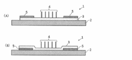
- FIG. 1A is a cross-sectional view for explaining the outline of the device 1 of the present invention.
- FIG. 1B is a cross-sectional view showing another configuration of the device 1 of the present invention.
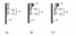
- FIGS. 2A to 2C show an example in which a nanowire is modified with a peptide and / or a nucleic acid that specifically recognizes a sample to be captured.
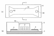
- 3A is a diagram showing an outline of the cover member 8 that covers the device 1
- FIG. 3B is a cross-sectional view taken along the line AA in FIG. 3A.
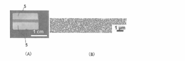
- FIG. 4A is a drawing-substituting photograph, which is a photograph of the manufactured device 1.
- FIG. 4A is a drawing-substituting photograph, which is a photograph of the manufactured device 1.
- FIG. 4B is a drawing substitute photograph, and is an enlarged photograph of a portion between the pair of electrodes 5 in FIG.
- FIG. 5 is a graph showing the relationship between the magnitude of the applied current and the temperature of the nanowire.
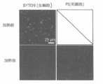
- FIG. 6 is a photograph substituted for a drawing, and is a fluorescent photograph of a sample before and after heating the device 1.
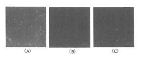
- FIG. 7A is a drawing-substituting photograph, which is a fluorescent photograph taken in Example 2.
- FIG. 7B is a drawing-substituting photograph, which is a fluorescent photograph taken in Comparative Example 1.
- FIG. FIG. 7C is a drawing-substituting photograph, which is a fluorescent photograph taken in Comparative Example 2.
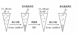
- FIG. 8 is a diagram showing an experimental procedure for investigating the relationship between peptide sequence and withdrawal temperature.
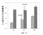
- FIG. 9 is a graph showing the binding rate of peptides to ZnO particles in Example 3.
- FIG. 10 is a graph showing the separation rate of peptides from ZnO particles in Example 3.
- nanowire device hereinafter sometimes simply referred to as “device”
- analysis apparatus including the device, a sample heat treatment method, and a sample separation method
- FIG. 1A is a cross-sectional view for explaining the outline of the device 1 of the present invention.
- a device 1 shown in FIG. 1A is in contact with an insulating substrate 2, a conductor layer 3 stacked on the insulating substrate 2, nanowires 4 formed on the conductor layer 3, and the conductor layer 3.
- a pair of electrodes 5 formed as described above is included. Note that the pair of electrodes 5 may be formed so as to be in contact with the conductor layer 3.
- FIG. 1B is a cross-sectional view showing another configuration of the device 1 of the present invention, in which a pair of electrodes 5 is formed on an insulating substrate 2 and a part of the conductor layer 3 is a pair of electrodes 5. The other part of the conductor layer 3 is laminated on the insulating substrate 2. That is, the pair of electrodes 5 may be formed on the conductor layer 3 or may be formed so as to be sandwiched between the insulating substrate 2 and the conductor layer 3.
- the insulating substrate 2 is not particularly limited as long as it does not conduct electricity. Glass; sapphire; silicon; alicyclic olefin polymer, epoxy compound, maleimide resin, (meth) acrylic resin, diallyl phthalate resin, triazine resin And resins such as polyphenylene ether.
- the conductor layer 3 is not particularly limited as long as it is a material capable of generating heat and generating heat by energizing the pair of electrodes 5.
- ZnO, Al 2 O 3, Si, Cr, Ti, Cu and the like are examples of the conductor layer 3 to be laminated.
- the thickness of the conductor layer 3 to be laminated may be appropriately adjusted in addition to the selection of the material.
- the nanowire 4 may be formed on the conductor layer 3 by a known method.
- the nanowire 4 may be grown by a known method by applying nanowire-forming particles or a catalyst.
- the nanowire-forming particles include ZnO.
- Nanowires using ZnO can be manufactured using a hydrothermal synthesis method. Specifically, first, ZnO is applied on the conductor layer 3. Next, a heated insulating substrate 2 in a precursor solution in which zinc nitrate hexahydrate (Zn (NO 3 ) 2 .6H 2 O) and hexamethylenetetramine (C 6 H 12 N 4 ) are dissolved in deionized water. ZnO nanowires can be grown by immersing. In addition, when ZnO is used as the conductor layer 3, the conductor layer 3 itself serves as a nanowire-forming particle, so that it is not necessary to separately apply ZnO to the conductor layer 3.
- Examples of the catalyst for producing the nanowire 4 include gold, platinum, aluminum, copper, iron, cobalt, silver, tin, indium, zinc, gallium, chromium, titanium, and the like.
- a nanowire using a catalyst can be produced by the following procedure. (A) A catalyst is deposited on the conductor layer 3.
- the nanowire 4 produced using a catalyst may be a nanowire having no branched chain, or may be a nanowire having a branched chain.
- a coating layer may be formed around the nanowire 4 as necessary.
- the coating layer when the device 1 is used for heat treatment of a sample, there is no particular limitation as long as the material has high thermal conductivity.
- the material When the device 1 is used for sample separation, since it is necessary to modify the nanowire 4 with a peptide and / or nucleic acid as described later, the material has a high thermal conductivity and has a binding property to the peptide and / or nucleic acid. Is preferred.
- the coating layer may be formed by a general deposition method such as sputtering, EB (Electron Beam) deposition, PVD (Physical Vapor Deposition), atomic layer deposition apparatus (ALD apparatus: Atomic Layer Deposition) after the nanowire 4 is formed. .
- a general deposition method such as sputtering, EB (Electron Beam) deposition, PVD (Physical Vapor Deposition), atomic layer deposition apparatus (ALD apparatus: Atomic Layer Deposition) after the nanowire 4 is formed. .
- the pair of electrodes 5 is not particularly limited as long as it is a commonly used electrode material such as platinum, gold, Ti, or Cr. It may be formed on the insulating substrate 2 or the conductor layer 3 by a method such as sputtering. The pair of electrodes 5 may be formed by stacking the above materials.
- a conductor layer 3 is stacked on an insulating substrate 2 by sputtering or the like, and then a pair of electrodes 5 is formed on the conductor layer 3 by sputtering or the like. . Then, if necessary, particles for forming the nanowire 4 or a catalyst may be applied to the conductor layer 3 between the pair of electrodes 5 to grow the nanowire 4.
- a pair of electrodes 5 is formed on an insulating substrate 2 by sputtering or the like, and then the insulating layer 2 and the pair of electrodes 5 are formed on the conductor layer 3 by sputtering or the like. Laminate on top. Then, if necessary, particles for forming the nanowire 4 or a catalyst may be applied to the conductor layer 3 to grow the nanowire 4.
- FIG. 2 shows an example in which the nanowire 4 is modified with a peptide and / or a nucleic acid (hereinafter sometimes referred to as “peptide or the like”) 6 that specifically recognizes the sample to be captured.
- FIG. 2A shows the nanowire 4 modified with a peptide or the like, and the peptide or the like 6 includes at least a nanowire adsorption site 61 and a sample recognition site 62.
- the nanowire adsorbing portion 61 can be separated from the nanowire 4 by heating or can be adsorbed on the nanowire 4 by changing the arrangement of peptides or the like.
- the sample recognition site 62 is not particularly limited as long as it is a sequence capable of specifically recognizing the capture target sample, and a known sequence or a sequence corresponding to the capture target sample may be determined by a known technique such as an antigen-antibody reaction.
- the sample to be captured is a nucleic acid
- the nanowire adsorption site 61 may be constituted by a nucleic acid that is adsorbed to the nanowire 4
- the sample recognition site 62 may be a sequence that hybridizes to the nucleic acid to be captured. If the sequences of peptides and nucleic acids are determined, they may be synthesized by a known peptide synthesizer or nucleic acid synthesizer. Alternatively, a peptide / nucleic acid contract synthesis service may be used. Modification of the nanowire 4 with a peptide or the like may be performed by immersing the nanowire 4 in a solution of a peptide or the like.
- FIG. 2 (B) is a diagram showing that the capture target sample S has been captured at the sample recognition site 62 of the nanowire 4 modified with the peptide 6 or the like.
- the capture target sample S can be heated by heating the nanowire 4. Therefore, it can be used for capturing specific bacteria in the sample solution and sterilizing by heating.
- FIG. 2 (C) is a diagram showing that the capture target sample S captured at the sample recognition site 62 is detached.
- the sample S to be captured such as captured bacteria is detached from the nanowire together with the peptide 6 modified to the nanowire 4 by heating the nanowire 4. Therefore, only the capture target sample S can be separated from the sample liquid by capturing the specific bacteria or the like in the sample solution and washing the sample liquid and then heating the nanowire 4.
- FIG. 3 is a diagram showing an example of sample heat treatment and sample separation using the device 1 of the present invention, and shows an example in which sample processing is continuously performed using the device 1.
- 3A is a diagram showing an outline of the cover member 8 that covers the device 1
- FIG. 3B is a cross-sectional view taken along the line AA in FIG. 3A.
- the cover member 8 has a channel 81 formed on the base material covering a portion where the nanowire 4 is formed when the cover member 8 is put on the device 1.
- a sample introduction hole 82 is formed at one end of the flow path 81 and a sample recovery hole 83 is formed at the other end so as to penetrate the surface of the cover member 8 and the flow path 81.
- the cover member 8 may be formed by cutting plastic or the like, or may be manufactured by preparing a mold and transferring it to polydimethylsiloxane (PDMS) or the like.
- PDMS polydimethylsiloxane
- sample liquid a liquid containing the sample
- sample liquid a liquid containing the sample
- a power source not shown
- the nanowire 4 may not be modified with the peptide 6 or the like.
- the sample liquid since the entire sample solution can be heat-treated, it can be used, for example, for water purification.
- the sample liquid may be recovered from the sample recovery hole 83.
- the sample-recognition site 62 is arranged so that the nanowire adsorption site 61 is not detached from the nanowire 4.
- the nanowire 4 may be modified with a peptide 6 having a sequence that recognizes specific bacteria and the like.
- the nanowire adsorption peptide 61 is arranged so that it is detached from the nanowire 4 by heating, and the sample recognition site 62 is a peptide 6 having a sequence for recognizing the bacteria or the like to be captured. 4 may be modified.
- the sample liquid is introduced from the sample introduction hole 82, and the sample liquid from which the capture target bacteria and the like are adsorbed and removed from the nanowire 4 is collected from the sample collection hole 83.
- a solution such as water or phosphate buffer that does not contain a sample is introduced from the sample introduction hole 82, and the nanowire 4 is heated via the conductor layer 3 by energizing the pair of electrodes 5. Since the nanowire adsorption site 61 is detached from the nanowire 4 by heating the nanowire 4, only the sample S to be captured can be separated from the sample liquid.
- the cover member 8 shown in FIG. 3A shows an example in which one sample insertion hole 82 and one sample collection hole 83 are formed, but a plurality of holes may be formed.
- a hole for introducing a solution such as water or a phosphate buffer may be formed in addition to the sample insertion hole 82.
- two sample recovery holes 83 are formed, one of which is used as a hole for recovering the sample liquid in which the bacteria to be captured are adsorbed and removed by the nanowire 4, and the other is a solution containing only the sample to be captured separated. It is good also as a hole to do.
- the height of the flow path 81 may be appropriately adjusted according to the processing purpose of the device 1.
- the height of the channel 81 is set to the nanowire so that heat can be easily transferred to the entire sample solution. It is desirable that the height be approximately the same as the height of 4.
- the height of the flow path 81 may be higher than that of the nanowire 4.
- the sample liquid in the flow path 81 is disturbed by alternately controlling the suction and ejection of the sample liquid.
- a flow may be generated so that the sample S to be captured is easily captured by the sample recognition site 62. It is preferable to increase the flow path 81, that is, to increase the cross-sectional area of the flow path 81, because the pressure at which the sample liquid flows is reduced, so that the sample liquid can be flowed easily.
- 3A and 3B show an example of use of the device 1 using the cover member 8, the device 1 is used to heat the sample solution, and the sample S to be captured is extracted from the sample solution.
- Other methods may be used as long as they can be separated.
- the nanowire 4 portion of the device 1 may be immersed in a sample solution placed in a petri dish or the like.
- the sample S to be captured is captured at the sample recognition site 62 of the peptide 6 or the like that has been modified into the nanowire 4 by being immersed in the sample solution, and then is collected in water or the like in another petri dish.
- the capture countermeasure sample S may be separated into water in another petri dish.
- the device 1 of the present invention can also be used as a sample pretreatment device for an analyzer.
- the sample liquid containing the separated capture target sample S is introduced into the analysis unit of the analyzer, whereby the sample can be analyzed.
- the analysis unit is not particularly limited as long as the sample can be analyzed.
- the entire apparatus can be downsized.
- Device 1 was produced by the following procedure. (1) Using a DC sputtering apparatus (SC-701MkII ADVANCE, Sanyu Denshi), on a silicon substrate (manufactured by Advantech), zinc oxide (ZnO) doped with 3 wt% of Al 2 O 3 has a thickness of about 100 nm. The layers were laminated as follows. (2) Next, after masking the portion where the nanowires 4 are to be formed, by using the above sputtering apparatus, titanium (Ti) is laminated to 10 nm, and platinum (Pt) is laminated to 100 nm thereon, A pair of electrodes was prepared. After the production of the electrode, the mask was removed.
- SC-701MkII ADVANCE Sanyu Denshi
- ZnO zinc oxide
- Al 2 O 3 aluminum oxide
- FIG. 4A is a photograph of the manufactured device 1.
- FIG. 4B is an enlarged photograph of a portion between the pair of electrodes 5 in FIG. As shown in FIG. 4B, it was confirmed that nanowires were formed on the ZnO layer (conductor layer) between the pair of electrodes.
- FIG. 5 is a graph showing the relationship between the magnitude of the applied current and the temperature of the nanowire. As shown in FIG. 5, it was found that the temperature of the nanowire 4 increases substantially linearly as the applied current is increased. Therefore, the temperature of the nanowire 4 can be adjusted by the magnitude of the applied current.
- Bacillus subtilis was prepared as a sample and cultured by an ordinary method until OD became 0.4.
- SYTO 9 live cell detection, which is two nuclear staining reagents having different cell membrane permeability, using a fluorescent reagent for detecting the viability of bacteria (Invitrogen: LIVE / DEAD (registered trademark) BacLight (registered trademark) Bacterial Viability Kit)) And PI (for dead cell detection) were co-stained.
- the cells stained with the nuclear staining reagent were dropped onto the device 1 with a pipette, and a current of 40 mA was applied for 30 seconds.
- the device 1 of the present invention can be used for heat treatment (heat sterilization) of cells and the like.
- sample separation experiment ⁇ Example 2> Next, a sample separation experiment was performed. When examining the temperature at which the peptide is released, it is difficult to measure the temperature of the nanowire 4 using a contact-type thermometer in the state where there is a sample solution around the nanowire 4. Therefore, sample separation experiments consisted of two experiments: capture of E. coli on peptide-modified nanowires 4 and peptide detachment when heating beads modified with fluorescent dye-labeled peptides. It verified about.
- the device 1 of Example 2 was produced according to the following procedure. (1) A device 1 was produced in the same procedure as in Example 1 except that the step of forming a pair of electrodes in the device 1 produced in Example 1 was omitted. (2) A peptide having the following amino acid sequence was synthesized by a conventional method and dissolved in phosphate buffered saline (PBS) to a concentration of 100 ⁇ M to prepare a peptide solution. [N] -GRHIFWRRGGGHKVPR- [C] (SEQ ID NO: 1) Among the above sequences, “HKVPR” on the C-terminal side binds to ZnO nanowires, and “GRHIWWRR” on the N-terminal side recognizes E.
- PBS phosphate buffered saline
- E. coli Since the sequence recognizing E. coli is a sequence recognizing lipopolysaccharide on the cell surface layer of Gram-negative bacteria, it can be applied to other than E. coli.
- the device 1 used in Example 2 was manufactured by the above procedure.
- E. coli sample A sample stained with E. coli was prepared by the following procedure. (1) SYTO9 was added to a PBS suspension of Escherichia coli (DH5 ⁇ ; Takara Bio Inc.) to a concentration of 1.5 ⁇ M. (2) Light-shielded and left at room temperature for 30 minutes. (3) Centrifugation was performed at 5,000 ⁇ g, and the supernatant was removed. (4) The centrifugal sediment was suspended in 1 mL of PBS. (5) The procedures (3) and (4) above were repeated three times. (6) It diluted with PBS so that it might become 5 * 10 ⁇ 7 > cells / mL, and E. coli suspension was produced.
- FIG. 7B is a fluorescent photograph taken in Comparative Example 1.
- FIG. 7C is a fluorescent photograph taken in Comparative Example 2.
- FIG. 8 shows the experimental procedure and the detailed procedure is described below.
- TBS-T pH 7.5, Tris buffer + 0.5% TWEEN 20
- 90 ⁇ l of the suspension of (1) was dispensed into 1.5 ml centrifuge tubes, 15 ⁇ l of 10 ⁇ M peptide solution (TBS) was added and stirred for 1 h.
- RCARRY SEQ ID NO: 2
- HYQSNW SEQ ID NO: 3 labeled with fluorescein isothiocyanate (FITC) were used.
- FITC fluorescein isothiocyanate
- FIG. 9 shows the fluorescence intensity obtained from 100 ⁇ l of a supernatant obtained by adding 90 ⁇ l of TBS-T not containing ZnO particles to 15 ⁇ l of a 10 ⁇ M peptide solution (TBS), and the resulting solution was dispensed onto the microtiter plate of (4) above. It is a graph which shows the coupling
- FIG. 10 shows the withdrawal rate calculated from the fluorescence intensity obtained from 100 ⁇ l of the supernatant of a solution obtained by adding 90 ⁇ l of TBS-T not containing ZnO particles to 15 ⁇ l of 10 ⁇ M peptide solution (TBS) and the measurement result measured in (8) above. It is a graph which shows. As is clear from FIG. 10, it was revealed that the peptide having the “RCARRY” sequence was released from the ZnO particles in a temperature-dependent manner. As described above, ZnO particles were used in Example 2 for the purpose of examining the peptide release temperature. However, it is clear that the peptide is released by heating the nanowire if the nanowire has the same composition.
- the sample to be captured can be separated by adjusting the temperature of the nanowire. Also. If the nanowire is not modified with a peptide, the sample can be sterilized by heating the nanowire. Therefore, the device 1 that can heat the nanowire of the present invention can be used in various ways.
- the device of the present invention can perform sample sterilization and sample separation with the same device. Therefore, since it can be used as a food sterilization apparatus in addition to the sample preparation apparatus of the analysis apparatus, it is useful for the analysis apparatus industry and the food industry.
Landscapes
- Chemical & Material Sciences (AREA)
- Life Sciences & Earth Sciences (AREA)
- Engineering & Computer Science (AREA)
- Health & Medical Sciences (AREA)
- Bioinformatics & Cheminformatics (AREA)
- Biotechnology (AREA)
- Wood Science & Technology (AREA)
- General Health & Medical Sciences (AREA)
- Organic Chemistry (AREA)
- Zoology (AREA)
- Genetics & Genomics (AREA)
- General Engineering & Computer Science (AREA)
- Biochemistry (AREA)
- Medicinal Chemistry (AREA)
- Analytical Chemistry (AREA)
- Microbiology (AREA)
- Nanotechnology (AREA)
- Biomedical Technology (AREA)
- General Physics & Mathematics (AREA)
- Virology (AREA)
- Tropical Medicine & Parasitology (AREA)
- Pathology (AREA)
- Immunology (AREA)
- Physics & Mathematics (AREA)
- Sustainable Development (AREA)
- Chemical Kinetics & Catalysis (AREA)
- Biophysics (AREA)
- Medical Informatics (AREA)
- Molecular Biology (AREA)
- Pharmacology & Pharmacy (AREA)
- Crystallography & Structural Chemistry (AREA)
- Hydrology & Water Resources (AREA)
- Apparatus Associated With Microorganisms And Enzymes (AREA)
- Micro-Organisms Or Cultivation Processes Thereof (AREA)
Applications Claiming Priority (2)
| Application Number | Priority Date | Filing Date | Title |
|---|---|---|---|
| JP2016-046302 | 2016-03-09 | ||
| JP2016046302A JP6758620B2 (ja) | 2016-03-09 | 2016-03-09 | ナノワイヤデバイス、該ナノワイヤデバイスを含む分析装置、サンプルの加熱処理方法及びサンプルの分離方法 |
Publications (1)
| Publication Number | Publication Date |
|---|---|
| WO2017154614A1 true WO2017154614A1 (ja) | 2017-09-14 |
Family
ID=59790353
Family Applications (1)
| Application Number | Title | Priority Date | Filing Date |
|---|---|---|---|
| PCT/JP2017/007030 Ceased WO2017154614A1 (ja) | 2016-03-09 | 2017-02-24 | ナノワイヤデバイス、該ナノワイヤデバイスを含む分析装置、サンプルの加熱処理方法及びサンプルの分離方法 |
Country Status (2)
| Country | Link |
|---|---|
| JP (1) | JP6758620B2 (cg-RX-API-DMAC7.html) |
| WO (1) | WO2017154614A1 (cg-RX-API-DMAC7.html) |
Cited By (1)
| Publication number | Priority date | Publication date | Assignee | Title |
|---|---|---|---|---|
| WO2020158832A1 (ja) * | 2019-01-30 | 2020-08-06 | Icaria株式会社 | 生体分子回収デバイス並びに方法、生体分子分析デバイス並びに方法 |
Families Citing this family (2)
| Publication number | Priority date | Publication date | Assignee | Title |
|---|---|---|---|---|
| LU100442B1 (en) * | 2017-09-19 | 2019-03-19 | Luxembourg Inst Science & Tech List | Gas sensor device with high sensitivity at low temperature and method of fabrication thereof |
| JP2020150930A (ja) | 2018-07-06 | 2020-09-24 | 国立大学法人東海国立大学機構 | 生体分子を分離するための流体デバイス及び方法 |
Citations (12)
| Publication number | Priority date | Publication date | Assignee | Title |
|---|---|---|---|---|
| JP2005035248A (ja) * | 2003-07-18 | 2005-02-10 | Toyota Motor Corp | 発熱有機ガラスおよび発熱有機ガラスの製造方法 |
| WO2005120205A2 (en) * | 2004-02-13 | 2005-12-22 | The Regents Of The University Of California | Room temperature deposition of nanotube transistor networks |
| JP2009127092A (ja) * | 2007-11-26 | 2009-06-11 | Konica Minolta Holdings Inc | 金属ナノワイヤ、及び金属ナノワイヤを含む透明導電体 |
| JP2011505688A (ja) * | 2007-11-28 | 2011-02-24 | コミサリア ア レネルジー アトミック エ オ ゼネルジー アルテルナティブ | 誘電体材料上に2つの電極を接続する半導体材料で作られたナノワイヤを成長する方法 |
| JP2011187901A (ja) * | 2010-03-11 | 2011-09-22 | Canon Inc | 半導体デバイスの製造方法 |
| WO2014065192A1 (ja) * | 2012-10-26 | 2014-05-01 | 国立大学法人名古屋大学 | 核酸抽出用デバイス及び該デバイスの製造方法、並びに核酸抽出方法及び核酸配列解析方法 |
| WO2014136913A1 (ja) * | 2013-03-06 | 2014-09-12 | 国立大学法人名古屋大学 | 生体分子の分離抽出用デバイス及びその製造方法、並びに生体分子の分離抽出方法 |
| JP2015050248A (ja) * | 2013-08-30 | 2015-03-16 | 国立大学法人大阪大学 | 非線形素子 |
| WO2015137427A1 (ja) * | 2014-03-12 | 2015-09-17 | 国立大学法人名古屋大学 | 生体分子抽出用チップ、及び生体分子抽出用チップの製造方法 |
| JP2016102758A (ja) * | 2014-11-28 | 2016-06-02 | 国立大学法人大阪大学 | 金属酸化物半導体センサ、および、その製造方法 |
| WO2016103561A1 (ja) * | 2014-12-22 | 2016-06-30 | パナソニックIpマネジメント株式会社 | 化学物質濃縮器および化学物質検出装置 |
| JP2017015661A (ja) * | 2015-07-06 | 2017-01-19 | 国立大学法人東京工業大学 | 金属結合性ペプチドのスクリーニング方法及び金属結合性ドメイン |
Family Cites Families (5)
| Publication number | Priority date | Publication date | Assignee | Title |
|---|---|---|---|---|
| KR20080005303A (ko) * | 2000-12-11 | 2008-01-10 | 프레지던트 앤드 펠로우즈 오브 하버드 칼리지 | 나노센서 |
| JP5409369B2 (ja) * | 2006-10-12 | 2014-02-05 | カンブリオス テクノロジーズ コーポレイション | ナノワイヤベースの透明導電体およびその適用 |
| US9140697B2 (en) * | 2009-03-18 | 2015-09-22 | The Regents Of The University Of California | Device for capturing circulating cells |
| EP2475612A4 (en) * | 2009-09-11 | 2017-09-13 | Jp Laboratories, Inc. | Monitoring devices and processes based on transformation, destruction and conversion of nanostructures |
| EP2539943B1 (en) * | 2010-02-24 | 2021-01-06 | Cambrios Film Solutions Corporation | Nanowire-based transparent conductors and methods of patterning same |
-
2016
- 2016-03-09 JP JP2016046302A patent/JP6758620B2/ja not_active Expired - Fee Related
-
2017
- 2017-02-24 WO PCT/JP2017/007030 patent/WO2017154614A1/ja not_active Ceased
Patent Citations (12)
| Publication number | Priority date | Publication date | Assignee | Title |
|---|---|---|---|---|
| JP2005035248A (ja) * | 2003-07-18 | 2005-02-10 | Toyota Motor Corp | 発熱有機ガラスおよび発熱有機ガラスの製造方法 |
| WO2005120205A2 (en) * | 2004-02-13 | 2005-12-22 | The Regents Of The University Of California | Room temperature deposition of nanotube transistor networks |
| JP2009127092A (ja) * | 2007-11-26 | 2009-06-11 | Konica Minolta Holdings Inc | 金属ナノワイヤ、及び金属ナノワイヤを含む透明導電体 |
| JP2011505688A (ja) * | 2007-11-28 | 2011-02-24 | コミサリア ア レネルジー アトミック エ オ ゼネルジー アルテルナティブ | 誘電体材料上に2つの電極を接続する半導体材料で作られたナノワイヤを成長する方法 |
| JP2011187901A (ja) * | 2010-03-11 | 2011-09-22 | Canon Inc | 半導体デバイスの製造方法 |
| WO2014065192A1 (ja) * | 2012-10-26 | 2014-05-01 | 国立大学法人名古屋大学 | 核酸抽出用デバイス及び該デバイスの製造方法、並びに核酸抽出方法及び核酸配列解析方法 |
| WO2014136913A1 (ja) * | 2013-03-06 | 2014-09-12 | 国立大学法人名古屋大学 | 生体分子の分離抽出用デバイス及びその製造方法、並びに生体分子の分離抽出方法 |
| JP2015050248A (ja) * | 2013-08-30 | 2015-03-16 | 国立大学法人大阪大学 | 非線形素子 |
| WO2015137427A1 (ja) * | 2014-03-12 | 2015-09-17 | 国立大学法人名古屋大学 | 生体分子抽出用チップ、及び生体分子抽出用チップの製造方法 |
| JP2016102758A (ja) * | 2014-11-28 | 2016-06-02 | 国立大学法人大阪大学 | 金属酸化物半導体センサ、および、その製造方法 |
| WO2016103561A1 (ja) * | 2014-12-22 | 2016-06-30 | パナソニックIpマネジメント株式会社 | 化学物質濃縮器および化学物質検出装置 |
| JP2017015661A (ja) * | 2015-07-06 | 2017-01-19 | 国立大学法人東京工業大学 | 金属結合性ペプチドのスクリーニング方法及び金属結合性ドメイン |
Cited By (2)
| Publication number | Priority date | Publication date | Assignee | Title |
|---|---|---|---|---|
| WO2020158832A1 (ja) * | 2019-01-30 | 2020-08-06 | Icaria株式会社 | 生体分子回収デバイス並びに方法、生体分子分析デバイス並びに方法 |
| JPWO2020158832A1 (cg-RX-API-DMAC7.html) * | 2019-01-30 | 2020-08-06 |
Also Published As
| Publication number | Publication date |
|---|---|
| JP6758620B2 (ja) | 2020-09-23 |
| JP2017158484A (ja) | 2017-09-14 |
Similar Documents
| Publication | Publication Date | Title |
|---|---|---|
| Chen et al. | Rapid enrichment of phosphopeptides and phosphoproteins from complex samples using magnetic particles coated with alumina as the concentrating probes for MALDI MS analysis | |
| US11059050B2 (en) | Magnetic capture of a target from a fluid | |
| JP5670194B2 (ja) | 多種類の標的を検出するためのマイクロ流体プラットフォーム | |
| CN102099666B (zh) | 用于从溶液浓缩颗粒的方法和系统 | |
| CN107034132B (zh) | 肿瘤细胞检测仪 | |
| KR101256628B1 (ko) | 나노입자를 이용한 미생물의 고속 검출방법 | |
| Pardoux et al. | Antimicrobial peptides as probes in biosensors detecting whole bacteria: a review | |
| JP4355214B2 (ja) | 発光試験測定用の固定化された脂質/タンパク質層を有するアッセイ用電極、その作製法、及びその使用法 | |
| Zhao et al. | Recent advances in microfluidics for the early detection of plant diseases in vegetables, fruits, and grains caused by bacteria, fungi, and viruses | |
| US11541393B2 (en) | Systems, apparatus, and methods for detecting pathogens | |
| JP6758620B2 (ja) | ナノワイヤデバイス、該ナノワイヤデバイスを含む分析装置、サンプルの加熱処理方法及びサンプルの分離方法 | |
| CN104011545B (zh) | 利用两种粒子的多功能生物材料接合体的制备方法及从中制得的多功能生物材料接合体 | |
| CN107338185B (zh) | 一种细胞或溶液中生物分子的捕获方法 | |
| US20020192676A1 (en) | Method for determining if a type of bacteria is present in a mixture | |
| WO2012094634A2 (en) | Functionalized carbon membranes | |
| CN109416312A (zh) | 利用表面附着结构的流动池,以及相关的系统和方法 | |
| CA2406133A1 (en) | Biosensor and related method | |
| CN108865655B (zh) | 一种单细胞捕获装置及捕获方法 | |
| US20140134263A1 (en) | Methods and Systems for Processing Exosomes | |
| EP1951741A2 (en) | Surface modification in a manipulation chamber | |
| JP6638913B2 (ja) | 生体物質検出用デバイス、生体物質検出用検出装置、イオン電流の測定方法、及び、生体物質の識別方法 | |
| WO2010119408A1 (en) | Up-concentration of organic microobjects for microscopic imaging | |
| CN101432739A (zh) | 超灵敏传感器和分析物的快速检测 | |
| ES2980804T3 (es) | Sistema fluídico de inmovilización y recogida de partículas en línea y método para usar el mismo | |
| WO2011154918A2 (en) | Diagnostic apparatus for immunoassay and diagnostic method for immunoassay using the same |
Legal Events
| Date | Code | Title | Description |
|---|---|---|---|
| NENP | Non-entry into the national phase |
Ref country code: DE |
|
| 121 | Ep: the epo has been informed by wipo that ep was designated in this application |
Ref document number: 17762954 Country of ref document: EP Kind code of ref document: A1 |
|
| 122 | Ep: pct application non-entry in european phase |
Ref document number: 17762954 Country of ref document: EP Kind code of ref document: A1 |