WO2017154242A1 - 半田接合装置および半田接合方法 - Google Patents
半田接合装置および半田接合方法 Download PDFInfo
- Publication number
- WO2017154242A1 WO2017154242A1 PCT/JP2016/076332 JP2016076332W WO2017154242A1 WO 2017154242 A1 WO2017154242 A1 WO 2017154242A1 JP 2016076332 W JP2016076332 W JP 2016076332W WO 2017154242 A1 WO2017154242 A1 WO 2017154242A1
- Authority
- WO
- WIPO (PCT)
- Prior art keywords
- substrate
- solder
- coil
- solder bonding
- ferrite
- Prior art date
- Legal status (The legal status is an assumption and is not a legal conclusion. Google has not performed a legal analysis and makes no representation as to the accuracy of the status listed.)
- Ceased
Links
Images







Classifications
-
- B—PERFORMING OPERATIONS; TRANSPORTING
- B23—MACHINE TOOLS; METAL-WORKING NOT OTHERWISE PROVIDED FOR
- B23K—SOLDERING OR UNSOLDERING; WELDING; CLADDING OR PLATING BY SOLDERING OR WELDING; CUTTING BY APPLYING HEAT LOCALLY, e.g. FLAME CUTTING; WORKING BY LASER BEAM
- B23K1/00—Soldering, e.g. brazing, or unsoldering
-
- B—PERFORMING OPERATIONS; TRANSPORTING
- B23—MACHINE TOOLS; METAL-WORKING NOT OTHERWISE PROVIDED FOR
- B23K—SOLDERING OR UNSOLDERING; WELDING; CLADDING OR PLATING BY SOLDERING OR WELDING; CUTTING BY APPLYING HEAT LOCALLY, e.g. FLAME CUTTING; WORKING BY LASER BEAM
- B23K1/00—Soldering, e.g. brazing, or unsoldering
- B23K1/002—Soldering by means of induction heating
-
- H—ELECTRICITY
- H05—ELECTRIC TECHNIQUES NOT OTHERWISE PROVIDED FOR
- H05K—PRINTED CIRCUITS; CASINGS OR CONSTRUCTIONAL DETAILS OF ELECTRIC APPARATUS; MANUFACTURE OF ASSEMBLAGES OF ELECTRICAL COMPONENTS
- H05K3/00—Apparatus or processes for manufacturing printed circuits
- H05K3/30—Assembling printed circuits with electric components, e.g. with resistors
- H05K3/32—Assembling printed circuits with electric components, e.g. with resistors electrically connecting electric components or wires to printed circuits
- H05K3/34—Assembling printed circuits with electric components, e.g. with resistors electrically connecting electric components or wires to printed circuits by soldering
-
- Y—GENERAL TAGGING OF NEW TECHNOLOGICAL DEVELOPMENTS; GENERAL TAGGING OF CROSS-SECTIONAL TECHNOLOGIES SPANNING OVER SEVERAL SECTIONS OF THE IPC; TECHNICAL SUBJECTS COVERED BY FORMER USPC CROSS-REFERENCE ART COLLECTIONS [XRACs] AND DIGESTS
- Y02—TECHNOLOGIES OR APPLICATIONS FOR MITIGATION OR ADAPTATION AGAINST CLIMATE CHANGE
- Y02P—CLIMATE CHANGE MITIGATION TECHNOLOGIES IN THE PRODUCTION OR PROCESSING OF GOODS
- Y02P70/00—Climate change mitigation technologies in the production process for final industrial or consumer products
- Y02P70/50—Manufacturing or production processes characterised by the final manufactured product
Definitions
- the present invention relates to a solder bonding apparatus and a solder bonding method for solder bonding by induction heating.
- solder is applied to the metal circuit portion of the substrate to mount the electronic component, and the electronic component is connected to the substrate while the solder is heated and melted by a method of blowing hot air from a reflow furnace or a nozzle.
- a method is mentioned. (See Patent Document 1).
- a heating element is brought into contact with an electronic component or the back surface of a substrate and the solder is heated and melted by heat conduction (see Patent Document 2).
- the heating range is wide, it is difficult to heat only a limited range on the substrate. That is, the region other than the region to be soldered on the substrate is easily affected by heat.
- a substrate made of an inexpensive alternative material such as polyester has a lower melting point and lower heat resistance than a substrate made of polyimide film. Since the conventional solder bonding method heats a wide range on the substrate, there is a concern that the substrate may be deformed as a result of the heating temperature becoming higher than the heat-resistant temperature of the substrate. In recent years, as electronic components have been miniaturized, there has been an increasing demand for heating a minute range on a substrate. In a conventional method having a wide heating range, such as a reflow method, it is difficult to heat only a very small range.
- the electrode portion is heated by heat conduction, so the heating efficiency is low. Therefore, as a result of excessively generating heat from the heating element, the film portion of the substrate is heated unnecessarily, and there is a concern that the substrate is easily thermally deformed. Furthermore, when a small electronic component is to be soldered, there is a concern that a higher-accuracy position control mechanism is required because the heating element must be brought into precise contact with the component.
- the present invention has been made in view of such circumstances, and when soldering the mounting components, it is possible to limit the heating range to a narrower range, and preferably avoid the substrate from being thermally deformed.
- the main object is to provide a solder bonding apparatus and a solder bonding method that can be used.
- This invention has the following configuration in order to achieve such an object.
- the solder bonding apparatus is a solder bonding apparatus using electromagnetic induction heating, and is disposed inside a coil that generates a magnetic field when current is supplied, and is a solder bonding target portion. And a soft ferrite that is in proximity to or in contact with the solder, and solder bonding is performed by supplying an electric current to the coil and inductively heating the portion to be soldered.
- the soft ferrite that is in close proximity to or in contact with the solder joining target portion of the substrate is disposed inside the coil.
- the conductor in the solder joining target portion can be induction heated. That is, the magnetic flux generated around the coil is transmitted by the soft ferrite so as to be focused on the solder joint target portion without being attenuated.
- the solder joint target portion can be easily set to a minute range. Therefore, even when a minute mounting component is bonded on the substrate, only the mounting range of the minute mounting component can be set as the induction heating range. Therefore, since the influence of induction heating on the film base material used for the substrate can be further reduced, deformation of the substrate due to heating can be suitably avoided.
- the soft ferrite with high magnetic permeability is close to or in contact with the solder bonding target site. Therefore, the magnetic flux generated around the coil is suitably transmitted to the part to be soldered by the soft ferrite. Therefore, even when the distance between the coil and the substrate is large, induction heating limited to a very small range can be suitably realized, so that the range in which the coil can be arranged in the solder bonding apparatus can be greatly widened.
- Soft ferrite is a soft magnetic material mainly composed of iron oxide. That is, since soft ferrite has a large electric resistance and hardly conducts current, eddy current is hardly generated in soft ferrite during induction heating.
- the soft ferrite itself since it is possible to avoid the soft ferrite itself from generating heat during induction heating, the influence of the heat received by the substrate can be further reduced even if the soft ferrite is close to or in contact with the part to be soldered. Therefore, even when an inexpensive material with low heat resistance is used for the substrate, it is possible to suitably avoid the substrate from being thermally deformed. As a result, induction heating limited to a minimum range in the substrate can be realized at a lower cost.
- the soft ferrite has a taper shape that tapers as it approaches the solder bonding target portion.
- the soft ferrite has a taper shape that tapers as it approaches the solder joining target portion. That is, since the soft ferrite is relatively thick in the portion close to the coil, more of the magnetic flux generated around the coil is transmitted to the solder joint target site through the soft ferrite having high magnetic permeability. Accordingly, it is possible to more suitably suppress the attenuation of the magnetic flux transmitted to the part to be soldered.
- the soft ferrite is relatively thin in the portion close to or in contact with the solder bonding target site, the area of the solder bonding target site on the substrate is smaller. Therefore, since the range to be subjected to induction heating can be limited to be narrower, it is possible to selectively solder the mounted component with a smaller size. Further, since the heating range can be made narrower, it is possible to avoid applying unnecessary heat to a conductor or the like in a region of the substrate where no mounting component is disposed. As a result, the substrate can be more preferably avoided from being deformed by induction heating.
- the soft ferrite is moved relative to the substrate including the solder bonding target portion, thereby changing the solder bonding target portion at a preset position on the substrate. It is preferable to provide position control means.
- the position control means is located at a preset position on the substrate by moving the soft ferrite relative to the substrate including the solder bonding target portion. Change the solder joint target part. That is, the position of the solder bonding target portion can be arbitrarily changed by the position control means. Therefore, by repeating the movement of the solder bonding target portion and induction heating, a predetermined region is arbitrarily selected for a plurality of regions located away from each other on the substrate, and is limited to only the selected region. Induction heating can be performed.
- the position control means is quickly controlled so that the soft ferrite is close to the solder joint target part. Induction heating can be performed again only for the bonding target portions. Therefore, it is possible to more suitably avoid the occurrence of defective solder bonding on the substrate.
- the soft ferrite is preferably a rod-shaped member disposed in a direction orthogonal to the surface of the substrate.
- the soft ferrite is a rod-shaped member arranged in a direction perpendicular to the surface of the substrate.
- the soft ferrite is rod-shaped, the distance between the coil and the substrate can be increased, and the solder joint target portion is in a narrower range. Therefore, it is possible to easily perform induction heating limited to a narrower range on the substrate while increasing the range in which the coils can be arranged.
- the soft ferrite is arranged in a direction perpendicular to the surface of the board, the magnetic flux generated around the coil and transmitted by the soft ferrite more reliably proceeds in the direction perpendicular to the surface of the board and is to be soldered.
- the site is irradiated.
- an eddy current is more preferably generated in the conductor located at the solder bonding target site, so that induction heating limited to the solder bonding target site can be performed more suitably.
- the soft ferrite is a plate-like member disposed in a direction orthogonal to the surface of the substrate.
- the soft ferrite is a plate-like member arranged in a direction orthogonal to the surface of the substrate.
- the magnetic flux generated around the coil and transmitted by the soft ferrite advances more reliably in the direction perpendicular to the surface of the board and is irradiated to the solder joint target part. Therefore, induction heating limited to the solder joint target part is performed. Can be performed more suitably.
- the solder joint target portion can be a strip-shaped range extending in one direction. In this case, it is possible to more suitably realize the solder bonding of the ends of the plurality of substrates having low heat resistance by using the conductor formed in a strip shape at the end of the substrate as a solder bonding target site.
- the soft ferrite is disposed above and below the solder joint target portion, respectively.
- the soft ferrite is disposed above and below the solder joining target part. That is, the solder joint target portion is sandwiched between soft ferrites.
- the magnetic flux generated in the coil is transmitted from one soft ferrite to the other soft ferrite via the solder joint target portion.
- the efficiency of induction heating at the solder bonding target site can be further improved.
- the coil is disposed on one of the upper and lower sides of the solder joint target portion, and one of the soft ferrites arranged above and below the solder joint target portion, respectively.
- the ferrite is a rod-like or plate-like member arranged in a direction orthogonal to the surface of the substrate inside the coil, and the other soft ferrite faces the one soft ferrite with the substrate interposed therebetween.
- it is preferable that it is a plate-shaped member arrange
- the coil is disposed on one of the upper side and the lower side of the part to be soldered.
- one soft ferrite is a rod-like or plate-like member arranged in the direction perpendicular to the surface of the substrate inside the coil It is.
- the other soft ferrite is a plate-like member arranged along the surface of the substrate so as to face one soft ferrite with the substrate interposed therebetween. That is, the magnetic flux generated in the coil is transmitted from one soft ferrite to the other soft ferrite disposed along the surface of the substrate via the solder bonding target portion.
- the magnetic flux irradiated to the solder joint target portion is more reliably transmitted to the other soft ferrite, attenuation of the magnetic flux irradiated to the solder joint target portion can be more preferably avoided.
- an eddy current is more preferably generated in the conductor located at the solder bonding target site, so that induction heating limited to the solder bonding target site can be performed more suitably.
- the present invention can also have the following configuration in order to achieve such an object.
- the solder bonding method includes a solder application step of applying a solder paste to a solder bonding target portion of a substrate on which a circuit pattern is formed, and mounting components to the solder bonding target portion to which the solder paste is applied.
- a current is supplied to the coil in a state where the mounting process and the soft ferrite disposed inside the coil that generates a magnetic field when current is supplied are brought close to or in contact with the solder joint target site.
- solder joining method of the present invention in the joining process, a current is supplied to the coil in a state where the soft ferrite disposed inside the coil is in proximity to or in contact with the solder joining target portion. Then, the solder bonding target portion is soldered by induction heating the solder bonding target portion.
- the shape and size of the portion where the soft ferrite comes close to or abuts it becomes easy to make the solder joint target portion a minute range. Therefore, even when a minute mounting component is bonded on the substrate, only the mounting range of the minute mounting component can be set as the induction heating range. Therefore, since the influence of induction heating on the film base material used for the substrate can be further reduced, deformation of the substrate due to heating can be suitably avoided.
- the soft ferrite having high magnetic permeability is close to or in contact with the solder joint target portion. Therefore, the magnetic flux generated around the coil is suitably transmitted to the part to be soldered by the soft ferrite. Therefore, even when the distance between the coil and the substrate is large, induction heating limited to a minute range can be suitably realized, so that the range in which the coil can be arranged in the solder bonding apparatus can be greatly widened.
- the heating range can be limited to a finer range, and the shape of the heating range can be controlled more precisely. Therefore, even a substrate made of a material having a melting point lower than that of a conventional substrate can perform solder bonding with higher accuracy to the substrate without being deformed by heat.
- FIG. 1 is a front view showing a schematic overall configuration of a solder joint system including a solder joint device according to a first embodiment.
- 1 is a perspective view illustrating a configuration of a solder bonding apparatus according to a first embodiment.
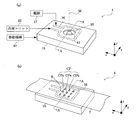
- (A) is a perspective view which shows the state which is not holding the board
- (b) is a perspective view which shows the state holding the board
- FIG. 3 is a cross-sectional view of the solder bonding apparatus shown in FIG.
- FIG. 6 is a front view illustrating a configuration of a solder bonding apparatus according to a modified example of the first embodiment. It is a front view which shows operation
- FIG. (A) is a front view which shows the structure which the coil and the board
- (b) is a coil and a board
- (c) is a front view which shows the structure of Example 1.
- FIG. 6 is a front view illustrating a configuration of a solder bonding apparatus according to a second embodiment.
- FIG. 6 is a diagram illustrating a configuration of a solder bonding apparatus according to a third embodiment. It is a figure which shows the structure which solder-joins substrates using the soldering apparatus which concerns on Example 3.
- FIG. (A) is a perspective view
- (b) is a front view. It is a front view which shows the structure of the soldering apparatus which concerns on a modification. It is a front view which shows the structure of the soldering apparatus which concerns on a modification.
- Embodiment 1 of the present invention will be described below with reference to the drawings.
- a case where a mounting component is bonded to an electrode portion of a circuit pattern formed on a substrate using the solder bonding apparatus according to the first embodiment will be described as an example.
- the solder bonding apparatus 4 includes a holding table 15, a coil 16, a power source 17, a ferrite material 41, and the like.
- the holding table 15 is made of an insulator that holds the substrate 7.
- the coil 16 has a shape that surrounds a predetermined region of the substrate 7 below the substrate 7.
- the lower side of the substrate 7 means a region facing the back side of the substrate 7.
- a power source 17 is connected to the coil 16. When an alternating current is supplied from the power supply 17 to the coil 16, a magnetic field is generated around the coil 16.
- the substrate 7 has a configuration in which a circuit pattern is formed at a predetermined pitch on a low heat resistant base film made of a belt-like polyester or polyethylene. As shown in FIG. 3, a solder paste P is applied to each of the electrodes 21 in the circuit pattern formed on the substrate 7. A mounting component CP is mounted on each of the electrodes 21 to which the solder paste P is applied.
- the ferrite material 41 is a rod-shaped member disposed on the inner side of the coil 16 on the back surface side of the substrate 7, and its tip is close to the substrate 7.
- the ferrite material 41 adjusts the magnetic field generated around the coil 16 so that a region (target region) facing the tip of the ferrite material 41 in the substrate 7 is a target of induction heating.
- the magnetic field generated around the coil 16 is adjusted by the ferrite material 41, and an eddy current is generated in the electrode 21 that is a conductor within the range of the target region in the substrate 7. That is, the electrode 21 located in the target region is induction-heated by the eddy current, and the solder paste is melted to join the mounting component CP and the electrode 21.
- the coil 16 has a pipe shape and is configured to circulate a cooling medium supplied from an externally connected cooling unit 22 inside.
- the holding table 15 is formed with a substantially annular recess 19 that surrounds a predetermined region R of the substrate 7 on the back side of the substrate 7.
- the region R in the first embodiment is a region where nine mounting components CP are mounted.
- the holding table 15 only needs to have a size including at least the predetermined region R, and the size and shape thereof can be appropriately changed.
- the coil 16 is a single substantially annular shape having the same shape as the concave portion 19 of the holding table 15, and is accommodated in the concave portion 19. That is, in Example 1, the coil 16 has a shape that surrounds the predetermined region R of the substrate 7 on the back surface side.
- the holding table 15 further includes a hole 20, and a ferrite material 41 is disposed inside the hole 20.
- the hole 20 is formed at a position surrounded by the coil 16.
- the shape of the hole 20 may be appropriately changed. As an example, the shape may be a recess, or may be a through-hole penetrating the holding table 15.
- the ferrite material 41 is a rod-shaped member arranged in a direction orthogonal to the surface of the substrate 7.
- the ferrite material 41 is preferably arranged along the axis of the coil 16. That is, as shown in FIG. 2A, the rod-shaped ferrite material 41 extends in the z direction, which is a direction perpendicular to the surface of the substrate 7, along the axis M of the coil 16 having a substantially annular shape. ing.
- the ferrite material 41 is made of soft ferrite and has a tapered configuration that tapers from the base end portion 41a toward the tip end portion 41b.
- soft ferrite is a soft magnetic material mainly composed of iron oxide, it efficiently transmits the magnetic flux generated from the coil 16 from the base end portion 41a to the tip end portion 41b.
- the transmitted magnetic flux is applied to the substrate 7 from the tapered tip end portion 41b.
- the conductor near the tip 41b generates heat with higher efficiency. That is, in the substrate 7, a local region facing the tip portion 41b of the ferrite material 41 is a region to be soldered in this embodiment.
- a region to be soldered is referred to as a “target region”.
- the target region T corresponds to a solder joint target site in the present invention.
- the distance between the tip 41b of the ferrite material 41 and the substrate 7 is preferably small.
- the tip portion 41 b may abut against the substrate 7 or may be close to the substrate 7.
- Example 1 when the holding table 15 holds the substrate 7 as shown in FIG. 2B, it is assumed that only the central mounting component CPa is included in the target region T among the nine mounting components CP. Note that the shape and size of the distal end portion 41b can be appropriately changed according to the range selected as the target region T.
- a moving mechanism 43 is connected to the holding table 15.
- the moving mechanism 43 moves the ferrite table 41 relative to the substrate 7 by appropriately moving the holding table 15 along the surface (xy plane) of the substrate 7.
- the position of the target region T on the substrate 7 is changed. Therefore, any position on the substrate 7 can be selected as the target region T by the moving mechanism 43.
- the moving mechanism 43 is controlled by the control unit 40.
- the moving mechanism 43 is not limited to a configuration that connects to the holding table 15 as long as the ferrite material 41 is moved relative to the substrate 7.
- a configuration in which the moving mechanism 43 is connected to the ferrite material 41 may be employed.
- the ferrite material 41 moves along the xy plane inside the coil 16.
- the coil 16 and the ferrite material 41 may be configured to be movable as a unit, and the moving mechanism 43 may be connected to the coil 16.
- the coil 16 and the ferrite material 41 are provided below the substrate 7 at positions facing the substrate surface of the substrate 7.
- the coil 16 and the ferrite 41 may be disposed above the substrate 7 at a position facing the substrate surface of the substrate 7.
- the upper side of the substrate 7 means a region facing the surface of the substrate 7 (surface on which the mounting component CP is mounted).
- the solder bonding apparatus is configured as described above.
- a round operation of mounting a mounting component on the substrate 7 using the solder bonding apparatus and performing solder bonding will be described with reference to FIGS.
- the substrate 7 is transferred to the holding table 15 of the solder bonding apparatus 4.
- the transported substrate 7 is sucked and held on the holding table 15.
- the predetermined region R on which the plurality of mounting components CP are mounted is surrounded on the back surface side of the substrate 7 by the coil 16 having a substantially annular shape.
- a magnetic flux F is generated around the coil 16, as shown in FIG.
- a ferrite material 41 made of soft ferrite is disposed at a position surrounded by the coil 16. Since soft ferrite has high permeability, the magnetic flux F generated from the coil 16 is transmitted from the base end portion 41a of the ferrite material 41 located near the coil 16 to the tip end portion 41b, and is not attenuated.
- the substrate 7 is irradiated from the portion 41b.
- the ferrite material 41 has a taper shape that tapers from a portion close to the coil 16 (base end portion 41a) toward a portion close to the substrate 7 (tip end portion 41b). Therefore, the magnetic flux F is focused on the tip portion 41 b along the shape of the ferrite material 41. The converged magnetic flux F is applied to the region of the substrate 7 facing the tip 41b, that is, the target region T.
- the conductor arranged within the target region T is induction-heated. That is, only the electrode 21 located within the target region T, that is, the electrode 21a among the plurality of electrodes 21 arranged on the substrate 7 is efficiently induction-heated.
- the electrode 21 located outside the target region T that is, the electrode 21 b and the electrode 21 c is not heated.
- the direction in which the magnetic flux F is applied to the target region T of the substrate 7 is a direction (z direction) perpendicular to the surface on which the circuit is formed on the substrate 7, so that it is disposed within the range of the target region T. Eddy currents are generated with higher efficiency in the current conductor.
- the solder paste P located within the target region T is melted by induction heating for a predetermined time. Therefore, among the mounted components positioned in the predetermined region R, the mounted component CPa positioned within the target region T is suitably soldered between the electrode 21a. Thus, the electromagnetic induction heating limited to the target region T, which is a local region on the substrate 7, is performed.
- a cooling medium is circulated in the coil 16 so that the coil 16 itself does not generate heat and thermally deform the substrate 7, and the coil 16 is kept at a predetermined temperature or less. Have been adjusted so that.
- the holding table 15 After performing solder bonding in the target region T, when performing solder bonding in another electrode 21, the holding table 15 is placed on the substrate surface (xy) so that the position of the other electrode 21 is within the range of the target region T. Move along the plane. By moving the ferrite material 41 relative to the surface of the substrate 7, the preset position of the target region T can be arbitrarily changed to a desired position.
- the moving mechanism 43 moves the holding table 15 from the position indicated by the dotted line to the position indicated by the solid line as shown in FIG. . Due to the movement of the holding table 15, the electrode 21 a is outside the range of the target region T, while the electrode 21 b is within the range of the target region T. Then, after moving the target region T to a desired position, a high frequency current is supplied from the power source 17 to the coil 16. In this case, only the electrode 21b located within the target region T is heated, and the electrode 21b and the mounting component CPb are soldered.
- the mounting component CP can be selectively soldered to each of the electrodes 21 arranged on the substrate 7.
- solder bonding By performing solder bonding on all the mounting components CP that require bonding, the operation of the solder bonding apparatus is completed.
- the predetermined region R in the substrate 7 is surrounded by the substantially annular coil 16 above or below the substrate 7, and the ferrite material 41 is disposed at a position surrounded by the approximately annular coil 16.
- the tip portion 41 b of the ferrite material 41 is configured so as to be close to and opposed to the target position T of the solder joint on the substrate 7. Since the ferrite material 41 is made of soft ferrite having high magnetic permeability, the magnetic flux F generated around the coil 16 travels through the ferrite material 41 to the target region T of the substrate 7 from the tip 41b. Irradiation in a direction perpendicular to the surface of
- the first embodiment is provided on the substrate 7. Since the electrode 21 is directly induction-heated, the heating efficiency for the solder paste P is high.
- the range to be heated in Example 1 can be limited to a very narrow range. That is, since the film portion of the substrate 7 can be avoided from being unnecessarily heated in the configuration of the first embodiment, even if the substrate 7 such as polyester having a heat resistant temperature lower than that of the polyimide film having high heat resistance is used, the substrate is heated by heat. 7 can be prevented from being deformed. Therefore, even when a low-cost material is used for the substrate 7, a suitable solder joint can be performed.
- the heating range by electromagnetic induction heating depends on the size of the coil 16. Since there is a limit to reducing the size of the substantially annular coil 16, it is very difficult to selectively induction-heat only a very small range in the substrate 7 in the configuration of the comparative example as shown in FIG. It is difficult to.
- the magnetic flux F generated around the coil 16 by the supply of the high-frequency current is transmitted to the substrate 7 through air having low permeability. Therefore, the magnetic flux F is easily attenuated as the distance from the coil 16 increases. Further, in the configuration of the comparative example, when the distance between the substrate 7 and the coil 16 is large, the magnetic flux F proceeds in a direction different from the z direction toward the substrate 7 (FIG. 9B). As a result, the magnetic flux F is applied to the substrate 7 in a direction different from the direction orthogonal to the surface of the substrate 7 (z direction), so that the efficiency of induction heating is reduced.
- the ferrite material 41 having high magnetic permeability is provided near the coil 16, and the tip portion 41 b is in close proximity to the substrate 7. Therefore, as shown in FIG. 9C, the magnetic flux F generated around the coil 16 is transmitted without being attenuated from the proximal end portion 41a of the ferrite material 41 to the distal end portion 41b, and from the distal end portion 41b to the substrate 7. Irradiated. Therefore, irradiation of the magnetic flux F limited to the range of the target area
- an eddy current is efficiently generated inside the conductor in the range of the target region T in the predetermined region R.
- the electrodes 21a within the target region T are heated with high heating efficiency, while the electrodes 21b and 21c outside the target region T are not heated.
- Example 1 using the ferrite material 41 the range in which induction heating is performed can be limited to the range of the target region T. Since the ferrite material 41 is composed of rod-shaped soft ferrite, it is easy to make the cross section of the tip end portion 41b in a minimum range. Therefore, it is possible to easily limit the range of the target region T in which induction heating is performed to a minimum range without depending on the size of the coil 16. In addition, since the shape of the target region T depends on the shape of the tip portion 41b, even if the region requiring heating is complicated by processing the tip portion 41b, precise induction heating limited to that region is performed. Can be executed.
- the ferrite material 41 having high magnetic permeability is close to the target region T of the substrate 7 through the tip 41b. (Or contact). Therefore, the magnetic flux F generated around the coil 16 is focused on the tip 41b by the ferrite material 41 and is preferably irradiated to the target region T. Therefore, in the solder bonding apparatus 4 according to the first embodiment, the possible arrangement range of the coil 16 can be significantly widened as compared with the comparative example.
- the ferrite material 41 has a tapered shape that tapers from the base end portion 41a toward the tip end portion 41b. That is, since the base end portion 41a has a large cross-sectional area, the distance between the base end portion 41a and the coil 16 becomes small. Therefore, since the magnetic flux F generated around the coil 16 is efficiently transmitted through the ferrite material 41, attenuation of the magnetic flux F transmitted to the target region of the substrate 7 can be suppressed more suitably.
- the tip portion 41b is tapered, the area of the target region T in the substrate 7 becomes smaller. Therefore, since the range to be subjected to induction heating can be limited to be narrower, it is possible to selectively solder the mounted component with a smaller size. Further, since the heating range can be made narrower, it is possible to avoid applying unnecessary heat to a region or the like in the substrate where no mounting component is arranged. By making the ferrite material 41 into a tapered shape, it is possible to further reduce the range of the target region T while increasing the transmission efficiency of the magnetic flux.
- the ferrite material 41 is composed of soft ferrite.
- Soft ferrite is a soft magnetic material mainly composed of iron oxide. That is, since soft ferrite has a large electric resistance and hardly passes current, eddy current is hardly generated in the ferrite material 41 during induction heating. Therefore, when the power source 17 supplies a high frequency current to the coil 16, it can be avoided that the ferrite material 41 itself generates heat. Therefore, even when the ferrite material 41 is brought close to the substrate 7, the influence of the heat received by the substrate 7 can be further reduced. As a result, even when an inexpensive material with low heat resistance is used for the substrate 7, it is possible to more suitably avoid the substrate 7 from being thermally deformed.
- the circuit pattern formed on the substrate 7 may include a conductor that is inconvenient when heated, such as a probing pad. Therefore, when the electrode to be soldered is close to the probing pad, the electrode and the probing pad are easily within the predetermined region R. As a result, when induction heating is performed in the configuration of the comparative example, the entire relatively large predetermined region R is heated, so that the probing pad is heated together with the electrodes, so that the performance of the substrate 7 is deteriorated. The problem is also a concern.
- the ferrite material 41 can be easily arranged and shaped (particularly, the tip 41b) so that only the electrode portion is within the target region T. And shape) can be adjusted.
- the conductor here, the electrode
- the solder joint apparatus which performs suitable solder joint can be implement
- the solder bonding apparatus 4 includes a moving mechanism 43 that moves the ferrite material 41 relative to the substrate 7.
- the moving mechanism 43 By controlling the moving mechanism 43, the position of the target region T can be arbitrarily changed. Therefore, by repeating the movement of the target region T by the moving mechanism 43 and the induction heating using the coil 16 and the ferrite material 41, a plurality of mounting components CP mounted at positions distant from the substrate 7, It is possible to perform induction heating limited to the mounting region of the arbitrarily selected mounting component CP.
- the ferrite material 41 is quickly moved so that the tip 41b is in close proximity to the mounting region of the mounting component CP. Induction heating can be performed again. Therefore, it is possible to suitably avoid the occurrence of defective solder joints on the substrate 7.
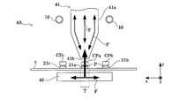
- solder joining apparatus according to the second embodiment is different from the first embodiment in that a ferrite material is provided on both sides of the substrate. It should be noted that the solder bonding apparatus according to the second embodiment is distinguished from the solder bonding apparatus 4 according to the first embodiment by attaching a reference numeral 4A. In the second embodiment shown in FIG. 10, the holding table 15 is not shown.
- the coil 16 and the rod-shaped ferrite material 41 are arranged above the substrate 7 as in the modification of the first embodiment shown in FIG.
- the ferrite material 41 is disposed on one of the upper and lower sides of the substrate 7 (here, above the substrate 7), and on the other of the upper and lower sides of the substrate 7 (here, below the substrate 7).
- a ferrite material 45 is disposed.
- the ferrite material 45 is made of soft ferrite and is disposed at a position that is in close proximity to the region of the substrate 7 including at least the target region T. That is, both sides of the target region T of the substrate 7 that is the purpose of induction heating are configured to be close to each other by the ferrite material 41 and the ferrite material 45. Like the ferrite material 41, the ferrite material 45 may be in contact with the substrate 7.
- the ferrite material 41 is provided only on one of the upper side and the lower side of the substrate 7. Therefore, since the magnetic flux F released from the tip 41b of the ferrite material 41 is transmitted through air having low permeability, the magnetic flux F directed from the tip 41b toward the substrate 7 is gradually attenuated. In addition, the direction of the magnetic flux F emitted from the tip portion 41 b is likely to change in a direction different from the direction perpendicular to the surface of the substrate 7.
- a ferrite material having high magnetic permeability is provided both above and below the substrate 7. That is, the ferrite material 45 is provided on the opposite side of the ferrite material 41 with the substrate 7 interposed therebetween.
- the magnetic flux F generated around the coil 16 is transmitted from the proximal end portion 41a of the ferrite material 41 to the distal end portion 41b, and from the distal end portion 41b to the target region of the substrate 7 It is efficiently transmitted to the ferrite material 45 having high magnetic permeability through T.
- the magnetic flux F applied to the target region T of the substrate 7 can more suitably avoid attenuation due to separation from the coil 16 as compared with the first embodiment. Further, the direction in which the magnetic flux F is applied to the target region T of the substrate 7 is more surely the direction perpendicular to the surface of the substrate 7. Therefore, since the eddy current is more efficiently generated in the conductor located within the range of the target region T, that is, the electrode 21a, the efficiency of induction heating in the target region T can be improved.
- the ferrite material 45 has a wide plate shape along the surface of the substrate 7. Further, the center of the ferrite material 45 is more preferably arranged so as to face the target region T as a center.
- the magnetic flux F transmitted from the ferrite material 41 to the target region T is more reliably transmitted to the ferrite material 45 located on the opposite side of the ferrite material 41 across the substrate 7.
- the heating efficiency can be further improved.
- the ferrite material 41 was a rod-shaped member disposed in a direction orthogonal to the surface of the substrate 7.
- the ferrite material 41 is the substrate 7. This is different from the other embodiments in that it is a plate-like member arranged in a direction perpendicular to the surface.
- the plate-like ferrite material 41 extends long in the direction (z direction) orthogonal to the surface of the substrate 7.
- the ferrite material 45 is provided as in the second embodiment, but the ferrite material 45 may be omitted as in the first embodiment.
- Example 3 since the ferrite material 41 is plate-shaped, the region of the substrate 7 facing the tip 41b, that is, the target region T is a thin strip extending in one predetermined direction.
- the plate-shaped ferrite material 41 is arranged so that the target region T is a strip-shaped region that is narrow in the length direction x of the substrate 7 and extends in the width direction y of the substrate 7 (FIG. 11).
- the mounting components CPa and CPb located within the target region T are soldered to the electrode 21.
- the mounting components CPc and CPd located outside the target region T are not joined. Therefore, efficient induction heating can be simultaneously performed on each of the plurality of mounting components CP arranged in the y direction while narrowing the range of induction heating in the x direction.
- FIG. 12A shows a structure in which a plurality of electrodes 21 extending in the x direction are arranged in the y direction with respect to the substrates 7a and 7b provided at the end portions in the length direction (x direction) of the substrate.
- a solder bonding apparatus 4B is arranged. Then, a high frequency current is supplied from the power supply 17 to the coil 16 in a state where the solder paste P is applied to the electrode 21.
- FIG. 12B is a cross-sectional view of the xz plane in FIG.
- the tip 41b of the ferrite material 41 is disposed so as to face each of the electrode 21 of the substrate 7a and the electrode 21 of the substrate 7b. That is, the target region T is a band-like region that extends long in the y direction, and each of the electrodes 21 extending in the x direction is located within the range of the target region T.
- the magnetic flux F generated around the coil 16 by the supply of electric current travels through the ferrite material 41 having high magnetic permeability and converges to the tip portion 41b.
- the converged magnetic flux F is irradiated from the front end portion 41b to the target regions T of the substrates 7a and 7b along the direction z perpendicular to the surface of the substrate 7. And since an eddy current generate
- the object to be induction-heated is limited to each of the conductors located within the target region T, that is, the electrodes 21, portions other than the electrodes 21 (for example, film portions) are unnecessary in the end portions of the substrate 7 a and the substrate 7 b. Can be avoided. Therefore, even when inexpensive and low heat resistant substrates are used, the substrates can be suitably soldered together while avoiding thermal deformation of the substrates. Further, by using the plate-shaped ferrite material 41, the target region T can be a band-shaped region extending in the y direction. For this reason, it is possible to suitably perform solder bonding by one induction heating for each of a large number of electrodes 21 arranged in the y direction.
- FIG. 1 is a front view illustrating a schematic overall configuration of a solder bonding system 51 including the solder bonding apparatus 4 according to the first embodiment.
- the configuration of the solder bonding apparatus provided in the solder bonding system 51 is not limited to the configuration of the first embodiment, and a solder bonding apparatus according to another embodiment or modification may be applied. *
- the solder bonding system 51 includes a substrate supply unit 1, a solder application unit 2, a mounting unit 3, a solder bonding apparatus 4, a cutting unit 5, a substrate recovery unit 6, and the like.
- the configuration of each part will be described in detail below.
- the configuration of the solder bonding apparatus 4 has been described in detail with reference to FIGS. 2 and 3 in the first embodiment, so that the description thereof is omitted here.
- a roll-shaped substrate 7 in which a predetermined circuit pattern is formed at equal intervals is loaded on a supply bobbin 8. That is, a circuit pattern is formed for each substrate 7 in the final form after the cutting process.
- the substrate 7 fed out from the supply bobbin 8 is wound and guided to the guide roller, and is guided in the order of the solder application unit 2, the mounting unit 3, the solder bonding apparatus 4, and the cutting unit 5.
- the supply bobbin 8 is given an appropriate rotational resistance and is configured so that excessive feeding is not performed on the substrate 7.
- the substrate 7 is made of a film made of a material having a lower heat resistance temperature than that of a polyimide film such as polyester and polyethylene.
- the polyimide film is not excluded.
- the material to be used is not limited to a film shape, and the thickness such as a sheet shape and a plate shape can be appropriately changed.
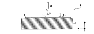
- the solder application unit 2 includes a holding table 9, an optical camera 10, a nozzle 11, and the like.
- the holding table 9 is, for example, a chuck table.
- the chuck table has a size larger than the width of the belt-like substrate 7 and longer than the length of the sheet to be cut into a predetermined length along the conveying direction, and is applied with solder. Any configuration that can keep the portion flat may be used. Therefore, the chuck table is not particularly limited as long as it is made of a plate or the like provided with a porous or suction hole on the holding plate that holds the substrate 7 by suction.
- the optical camera 10 images a circuit pattern formed on the substrate 7.
- the imaging result is transmitted to the control unit 40, and a pattern matching process is performed between the reference image of the circuit pattern recorded in advance and the actual image, and the position coordinates of each electrode on which the mounting component is mounted is obtained.
- the nozzle 11 is configured to move left and right when the front view of FIG. 1 is viewed by a driving mechanism and to move up and down in the height direction. That is, the nozzle 11 applies a predetermined amount of solder paste to the position of the electrode coordinates obtained by the control unit 40.
- the mounting unit 3 includes a holding table 13 and a mounting device 14.
- the holding table 13 is a chuck table, for example, like the holding table 9 of the solder application unit 2.
- the chuck table has a size larger than the width of the belt-like substrate 7 and longer than the length of the sheet to be cut into a predetermined length along the conveying direction, and is applied with solder. Any configuration that can keep the portion flat may be used. Therefore, the chuck table is not particularly limited as long as it is made of a plate or the like provided with a porous or suction hole on the holding plate that holds the substrate 7 by suction.
- the mounting device 14 includes a taping machine and a mounter.
- a taping machine (not shown) accommodates a plurality of mounting parts CP (for example, chip capacitors and chip resistors) on an embossed carrier tape at a predetermined pitch, and loads a tape reel whose surface is covered with a cover tape, The cover tape is taken up and collected while being peeled off.
- CP for example, chip capacitors and chip resistors
- the mounter is configured to move left and right when viewed from the front in FIG. 1 and to move up and down in the height direction. Therefore.
- the mounter is configured to suck and hold the mounting component CP from the carrier tape and mount it on a predetermined electrode based on the position coordinates of the electrode acquired by the camera.
- the mounter may use a bonding device depending on the size and type of the mounted component.
- the bonding apparatus includes a bonding head that moves left and right when viewed from the front in FIG. 1 and that can move up and down in the height direction.
- the bonding head conveys the mounting component CP (for example, a chip capacitor and a chip resistor) while holding it by a collet attached to the lower end.
- the cutting unit 5 includes a holding table 23 and a laser device 24 as shown in FIGS. 1 and 8.
- the holding table 23 is a chuck table larger than the width of the belt-like substrate 7, and a cutting groove 25 is formed along the width direction of the substrate 7. Note that suction holes are also formed in the cutting groove 25, and smoke and dust generated during cutting are sucked and removed.
- the laser device 24 is configured to be horizontally movable along a cutting groove 25 formed in the width direction of the substrate 7.
- the cutting of the substrate 7 is not limited to the laser device 24, and may be a cutter blade, for example.
- the substrate recovery unit 6 includes a conveyor 26 that is an endless belt that conveys the substrate 7 that has been cut into single sheets by the cutting unit 5, and a collection container 27 that is disposed at the end in the conveyance direction of the conveyor 26. Yes.
- the conveyor 26 may intermittently convey the single substrate 7 in synchronization with the intermittent conveyance in the previous process, or may be operated continuously.
- nip rollers 30 to 34 are provided in front of and behind the solder application unit 2, the mounting unit 3, the solder bonding apparatus 4, and the cutting unit 5, respectively.
- Each of the nip rollers 30 to 34 includes a driving roller and a driven roller, and is configured to be driven by the intermittent feeding and conveyance of the substrate 7 from the substrate supply unit 1.
- solder bonding system including the solder bonding apparatus according to the present embodiment is configured as described above. A single operation of mounting a mounting component on the substrate 7 and performing solder bonding using the solder bonding system will be described with reference to FIGS.
- a roll of the substrate 7 in which a circuit pattern is formed at a predetermined pitch on a low heat resistant base film made of a strip-like polyester or polyethylene manufactured in the previous process is loaded on the bobbin 8 of the substrate supply unit 1.
- the substrate 7 is pulled out from the roll to the cutting unit 5 and set, and predetermined conditions such as a feeding pitch are initialized from the control unit 40.
- the device When the initial setting is completed, the device is activated.
- the back surface of the area of the sheet unit to be cut is sucked and held by the holding table 9 of the solder application unit 2.
- the optical camera 10 images the area of the substrate 7 held by suction.
- the control unit 40 performs pattern matching processing between the actual image acquired by the optical camera 10 and the reference image of the circuit pattern stored in advance, and obtains the coordinates of the electrode 21 in the circuit pattern.
- the nozzle 11 applies the solder paste P to each of the electrodes 21 while moving based on the electrode coordinates as shown in FIG.
- the substrate 7 is released from the suction by the holding table 9 and is transported to the mounting unit 3.
- the nip rollers 31 and 32 have a stepped shape that contacts only both ends of the substrate 7, it is preferable that the nip rollers 31 and 32 have a structure that does not contact the area where the solder paste P is applied.
- the upper roller may be raised so that the nip of the substrate 7 is released so that the solder paste P does not contact the upper roller.
- the substrate 7 coated with the solder paste P reaching the mounting portion 3 is sucked and held by the holding table 13.
- the mounting device 14 of the mounting unit 3 operates the bonding head based on the electrode coordinates acquired in advance by the solder application unit 2 and sucks and conveys the mounting component CP from the carrier tape. As shown in FIG. It mounts in order on the predetermined electrode.
- the substrate 7 is transferred to the solder bonding apparatus 4.
- the board 7 reaches the solder bonding apparatus 4, the board 7 is sucked and held on the holding table 15.
- the step of performing solder bonding using the solder bonding apparatus 4, that is, the bonding step is as described in detail in the first embodiment. That is, when a current is applied from the power source 17 to the coil 16, a magnetic flux F is generated around the coil 16, as shown in FIG.
- the magnetic flux F generated from the coil 16 is transmitted from the proximal end portion 41a of the ferrite material 41 located near the coil 16 to the distal end portion 41b and converges to the distal end portion 41b without being attenuated. Since the converged magnetic flux F advances in the z direction and is irradiated onto the target region T on the substrate 7, an eddy current is generated in the conductor disposed within the target region T, and the conductor is induction-heated. That is, only the electrode 21a located within the target region T among the plurality of electrodes 21 arranged on the substrate 7 is efficiently induction-heated (see FIG. 3).
- the mounted component CPa positioned within the target region T is suitably soldered to the electrode 21a.
- the electromagnetic induction heating limited to the target region T, which is a local region on the substrate 7, is performed.
- the movement of the target region T and induction heating by the coil 16 are appropriately repeated so that the electrode 21 disposed on the substrate 7 is replaced.
- the mounting component CP is selectively soldered.
- the joining process is completed by performing solder joining on all the mounting components CP that require solder joining.
- the suction of the substrate 7 by the holding table 15 is released, and the substrate 7 to which the mounting component CP is soldered is conveyed to the cutting unit 5.
- the solder-bonded substrate 7 reaches the cutting part 5 and is held by suction by the holding table 23.
- the substrate 7 is cut by the laser device 24 at the rear end of the sheet.
- the cut substrate 7 is fed to the conveyor 26 by a nip roller 34 held on the leading end side in the transport direction.
- the substrate 7 placed on the conveyor 26 is transported to the collection container 27 and collected.
- the soldering system 51 completes the one-round operation of mounting the mounting component CP on the substrate 7 and soldering.
- the one-round operation is carried out by intermittent conveyance of the substrate 7, and the processing is repeated in order for each sheet having a circuit pattern formed on the belt-like substrate 7.
- the present invention is not limited to the above embodiment, and can be modified as follows.
- the coil 16 and the ferrite material 41 are both arranged on the same side of the substrate 7, but the arrangement of the ferrite material 41 is not limited to this. That is, if the ferrite material 41 is disposed along the axis M of the coil 16, the coil 16 and the ferrite material 41 may be disposed on opposite sides of the substrate 7. That is, as shown in FIG. 13A, the coil 16 may be disposed below the substrate 7 and the ferrite material 41 may be disposed above the substrate 7. Further, the coil 16 may be disposed above the substrate 7 and the ferrite material 41 may be disposed below the substrate 7.
- the substrate 7 when performing solder bonding, the substrate 7 is held in a horizontal position as shown in FIG.
- the posture for holding the substrate 7 is not limited to the horizontal posture.
- FIG. 14 a configuration in which the substrate 7 takes a standing posture can be mentioned.
- the coil 16 and the ferrite material 41 are provided above the substrate 7, that is, at positions facing the circuit surface (surface on which the mounting component CP is mounted) of the substrate 7. Show.
- Example 1 shown in FIG. 1 the vertical direction coincides with the z direction.
- the vertical direction matches the x direction.
- the ferrite material 41 has a taper shape that tapers from the proximal end portion 41a close to the coil 16 toward the distal end portion 41b close to the target region T.
- the shape of the ferrite material 41 is not limited to a tapered shape, and may be a bar shape or a flat plate shape having the same thickness from the base end portion 41a to the tip end portion 41b.
- the ferrite material 41 is more preferably tapered in that the magnetic flux F generated around the coil 16 can be suitably transmitted and converged to the tip portion 41b.
- the holding table 15 of the solder bonding apparatus 4 may be a chuck table.
- the chuck table includes a holding plate having a suction hole and a suction device. Note that the chuck table is not limited to the configuration, and may be porous such as ceramic.
- the substrate 7 is kept flat by the chuck table. That is, since the coil 16 and the substrate 7 can be kept parallel, the magnetic flux having a high magnetic flux density is reliably irradiated in the direction perpendicular to the surface of the substrate 7 with respect to the electrode 21 positioned within the target region T. Can be made. Therefore, the efficiency of induction heating limited to the target region T can be further improved.
- the substantially annular coil 16 is provided in one stage above or below the substrate 7, but is not limited thereto. That is, a configuration in which a plurality of single substantially annular coils 16 having the same shape are provided may be used. For example, two or more coils 16 may be arranged above the substrate 7. One or more coils 16 may be arranged above and below the substrate 7, respectively. Further, as the coil 16, a coil wound a plurality of times may be used instead of the one-turn coil.
- the magnetic flux in the range of induction heating is larger than that of a single coil.
- the vertical magnetic flux portion is expanded as compared with the case where a single coil is used. Therefore, it is possible to irradiate the electrode 21 in the target region T with a magnetic flux having a higher magnetic flux density. Therefore, the efficiency of induction heating limited to the target region T can be further improved as compared with the case where a single coil is used.
- solder paste is used to connect the mounting component CP to the electrode 21.
- a solder ball may be used instead of the solder paste.
- the coil 16 has a configuration that is substantially annular along the surface of the substrate 7, but the shape of the coil 16 is not limited to a substantially annular shape. As long as the ferrite material 41 disposed inside the coil 16 is configured to focus the magnetic flux F around the coil 16 on the tip portion 41b, the shape of the coil 16 may be changed as appropriate.
- the ferrite material 41 or the ferrite material 45 is made of soft ferrite, that is, magnetic ceramics manufactured by molding and sintering using iron oxide as a main material (hereinafter referred to as “narrowly defined soft ferrite”). ).
- soft ferrite that is, magnetic ceramics manufactured by molding and sintering using iron oxide as a main material
- these ferrite materials are not limited to soft ferrite in the narrow sense.
- the soft ferrite is not only a soft ferrite in a narrow sense but also a concept including a substitute material for a soft ferrite in a narrow sense showing the same characteristics as the soft ferrite in a narrow sense in terms of electrical resistance and magnetic permeability. It shall mean soft ferrite.
- the ferrite material 45 has been described by taking as an example a configuration in which the ferrite material 45 is a plate-like member disposed along the surface of the substrate 7. It is not limited to this. That is, as shown in FIG. 13B, the ferrite material 45 may have a rod-like or plate-like configuration arranged along the axis of the coil 16, similarly to the ferrite material 41. Also in the configuration according to the modification (9), the magnetic flux F is efficiently transmitted along the ferrite material 41 and the ferrite material 45 extending in the z direction. Therefore, since the magnetic flux F is focused and irradiated on the target region T, induction heating limited to the target region T is performed.
- the solder bonding device 4 is ferrite so as to be surrounded by the coil 16 as shown in FIG. 3. It is not restricted to the structure by which the material 41 is arrange
- FIG. 13C illustrates a configuration in which the ferrite material 45 is not provided below the substrate 7, the substrate 7 is opposed to the ferrite material 41 with the substrate 7 interposed therebetween as in FIGS. 10 and 13B.
- a configuration further including a ferrite material 45 such as a rod shape or a plate shape may be employed.
Landscapes
- Engineering & Computer Science (AREA)
- Mechanical Engineering (AREA)
- Manufacturing & Machinery (AREA)
- Microelectronics & Electronic Packaging (AREA)
- Electric Connection Of Electric Components To Printed Circuits (AREA)
Abstract
基板7上で実装部品CPの実装された所定領域Rを、当該基板7の上方または下方において囲う形状のコイル16を配置する。加熱対象となる電極21および実装部品CPを含む対象領域Tに対向するフェライト材41を配置する。コイル16の周りに発生する磁束Fは、効率よくフェライト材41を伝って集束し、集束した磁束Fは基板7の対象領域Tを垂直方向に照射される。従って、基板7において対象領域Tの範囲内に位置する電極21に限定した誘導加熱が行われるので、対象となる電極21および実装部品CPのみを選択的に半田で接合することができる。
Description
本発明は、誘導加熱によって半田接合する半田接合装置および半田接合方法に関する。
プリント基板の表面にパターン形成された、電極などの金属回路に対して、チップコンデンサおよびチップ抵抗などの電子部品を実装する場合、半田接合によって両者を接続させる方法が広く用いられている。
従来の半田接合方法としては、基板の金属回路部分に半田を塗布して電子部品を実装させ、リフロー炉やノズルから熱風を吹き付ける方式などによって、半田を加熱溶融させながら基板に電子部品を接続する方法が挙げられる。(特許文献1を参照)。また他の従来方法として、発熱体を電子部品や基板の裏面などに当接させ、熱伝導によって半田を加熱溶融させる方法も用いられている(特許文献2を参照)。
しかしながら、現在の主流であるリフロー方式においては、加熱範囲が広いので、基板上の限られた範囲のみを加熱することが困難である。すなわち、基板において半田接合の対象となる領域以外も容易に熱の影響を受けることとなる。
近年のスマートフォンなどの携帯電子機器、ウェアラブル機器およびLED照明機器などは、軽量化が要求されている。そこで、小型の表面実装タイプの電子部品およびLEDなどのチップ部品を基板に実装している。また、基板のコストを削減するために、基板の材料をポリイミドフィルムに代えてポリエステルまたはポリエチレンなどが利用されつつある。
しかしながら、ポリエステルなどの安価な代替材料からなる基板は、ポリイミドフィルムからなる基板よりも融点が低く耐熱性に劣る。従来の半田接合方法では基板上の広い範囲を加熱するので、基板の耐熱温度よりも加熱温度が高くなる結果、当該基板を変形させてしまうといった問題が懸念される。近年では電子部品の微小化が進んでいるので、基板上における微小な範囲を加熱させる要求が大きくなっている。リフロー方式など、加熱範囲が広い従来の方法では、微小範囲に限定して加熱することは困難である。
また、基板以外に発熱体を用意して当該発熱体を基板等に当接させる方式による従来の半田接合方法では、熱伝導により電極部分を加熱するので、加熱効率が低い。そのため発熱体を過度に発熱させる結果、基板のフィルム部分が無用に加熱されるので、基板が容易に熱変形するという問題が懸念される。さらに、微小な電子部品を半田接合の対象とする場合、当該部品に発熱体を正確に当接させる必要があるので、より高精度な位置制御機構が要求されるという問題も懸念される。
本発明はこのような事情に鑑みてなされたものであって、実装部品を半田接合する際に、加熱範囲をより狭い範囲に限定することを可能とし、基板が加熱変形することを好適に回避できる半田接合装置および半田接合方法を提供することを主たる目的としている。
この発明は、このような目的を達成するために、次のような構成をとる。
すなわち、本発明に係る半田接合装置は、電磁誘導加熱を利用した半田接合装置であって、電流が供給されることで磁界が発生するコイルと、前記コイルの内側に配置され、半田接合対象部位に近接または当接するソフトフェライトと、を備え、前記コイルに電流を供給して前記半田接合対象部位を誘導加熱することにより半田接合することを特徴とするものである。
[作用・効果]本発明に係る半田接合装置によれば、基板の半田接合対象部位に近接または当接するソフトフェライトを、コイルの内側に配置する。このような構成により、当該半田接合対象部位内の導体のみを誘導加熱することができる。すなわち、コイルの周りに発生する磁束はソフトフェライトによって、減衰することなく半田接合対象部位へ集束するように伝えられる。
そして、ソフトフェライトが近接または当接する部分の形状およびサイズを調整することにより、半田接合対象部位を容易に微小な範囲とすることができる。そのため、基板上に微小な実装部品を接合させる場合であっても、当該微小な実装部品の実装範囲のみを誘導加熱の範囲とすることができる。したがって、基板に用いられるフィルム基材に対する誘導加熱の影響をより小さくできるので、加熱による基板の変形を好適に回避できる。
また、本発明に係る構成では、コイルと基板との距離が離れている場合であっても、透磁性の高いソフトフェライトが半田接合対象部位に近接または当接している。そのため、コイルの周りに発生する磁束はソフトフェライトによって好適に半田接合対象部位へ伝えられる。従って、コイルと基板との距離が離れている場合であっても、微小範囲に限定した誘導加熱を好適に実現できるので、半田接合装置におけるコイルの配置可能範囲を大幅に広くできる。
また、ソフトフェライトは酸化鉄を主成分とする軟質磁性材料である。すなわち、ソフトフェライトは電気抵抗が大きく、電流をほとんど通さないので、誘導加熱の際にソフトフェライトにおいて渦電流が発生しにくい。
そのため、誘導加熱を行う際にソフトフェライト自体が発熱することを回避できるので、ソフトフェライトが半田接合対象部位に近接または当接する構成であっても、基板が受ける熱の影響をより小さくできる。従って、耐熱性の低い安価な材料を基板に用いる場合であっても、基板が熱変形することを好適に回避できる。その結果、基板における極小範囲に限定した誘導加熱を、より低いコストで実現できる。
また、上述した発明において、前記ソフトフェライトは、前記半田接合対象部位に近づくにつれて先細りとなるテーパ状となっていることが好ましい。
[作用・効果]本発明に係る半田接合装置によれば、ソフトフェライトは、半田接合対象部位に近づくにつれて先細りとなるテーパ状となっている。すなわちソフトフェライトはコイルに近い部分において比較的太くなっているので、コイルの周りに発生する磁束のより多くが透磁性の高いソフトフェライトを介して半田接合対象部位へ伝えられる。従って、半田接合対象部位へ伝えられる磁束の減衰をより好適に抑えることができる。
一方で、ソフトフェライトは半田接合対象部位に近接または当接する部分において比較的細くなっているので、基板における半田接合対象部位の面積はより小さくなる。従って、誘導加熱の対象となる範囲をより狭く限定できるので、より小型化された実装部品を選択的に半田接合させることが可能となる。また加熱範囲をより狭くできるので、基板のうち実装部品が配設されていない領域にある導体などに対して、無用に熱を加えることを回避できる。その結果、誘導加熱によって基板が変形することをより好適に回避できる。
また、上述した発明において、前記半田接合対象部位を含む前記基板に対して、前記ソフトフェライトを相対的に移動させることにより、前記基板上の予め設定した位置にある前記半田接合対象部位を変更する位置制御手段を備えることが好ましい。
[作用・効果]本発明に係る半田接合装置によれば、位置制御手段は半田接合対象部位を含む基板に対してソフトフェライトを相対的に移動させることにより、基板上の予め設定した位置にある半田接合対象部位を変更する。すなわち位置制御手段により、半田接合対象部位の位置を任意に変更できる。そのため、半田接合対象部位の移動と、誘導加熱とを繰り返すことにより、基板において離れた位置にある複数の領域に対して、所定の領域を任意に選択し、当該選択された領域のみに限定された誘導加熱を行うことができる。
また、誘導加熱の後、所定の半田接合対象部位において加熱不足による半田接合の不良が判明した場合、速やかに当該半田接合対象部位にソフトフェライトが近接するように位置制御手段を制御し、当該半田接合対象部位のみについて再度誘導加熱を行うことができる。従って、基板における半田接合の不良の発生をより好適に回避できる。
また、上述した発明において、前記ソフトフェライトは、前記基板の面に直交する方向に配置されている棒状の部材であることが好ましい。
[作用・効果]本発明に係る半田接合装置によれば、ソフトフェライトは、前記基板の面に直交する方向に配置されている棒状の部材である。この場合、ソフトフェライトは棒状であるので、コイルと基板との距離を大きくできるとともに、半田接合対象部位がより狭い範囲となる。従って、コイルの配置可能範囲をより広くしつつ、基板におけるより狭い範囲に限定した誘導加熱を容易に行うことができる。
また、ソフトフェライトは基板の面に直交する方向に配置されているので、コイルの周りに発生し、ソフトフェライトによって伝えられる磁束は、より確実に基板の面に直交する方向へ進んで半田接合対象部位に照射される。その結果、半田接合対象部位に位置する導体において、渦電流がより好適に発生するので、半田接合対象部位に限定した誘導加熱をより好適に行うことができる。
また、上述した発明において、前記ソフトフェライトは、前記基板の面に直交する方向に配置されている板状の部材であることが好ましい。
[作用・効果]本発明に係る半田接合装置によれば、ソフトフェライトは、基板の面に直交する方向に配置されている板状の部材である。この場合、コイルの周りに発生し、ソフトフェライトによって伝えられる磁束は、より確実に基板の面に直交する方向へ進んで半田接合対象部位に照射されるので、半田接合対象部位に限定した誘導加熱をより好適に行うことができる。
また、ソフトフェライトは板状であるので、半田接合対象部位を一方向に伸びている帯状の範囲とすることができる。この場合、基板の末端において帯状に形成された導体を半田接合対象部位とすることにより、耐熱性の低い複数の基板の末端同士を半田接合することを、より好適に実現できる。
また、上述した発明において、前記ソフトフェライトは、前記半田接合対象部位の上方および下方にそれぞれ配置されていることが好ましい。
[作用・効果]本発明に係る半田接合装置によれば、ソフトフェライトは、半田接合対象部位の上方および下方にそれぞれ配置されている。すなわち半田接合対象部位はソフトフェライト同士によって挟まれる構成となっている。この場合、コイルにおいて発生した磁束は、一方のソフトフェライトから半田接合対象部位を経由して、他方のソフトフェライトへと伝えられる。そのため、半田接合対象部位の上方および下方のうち一方のみにソフトフェライトを配置する構成と比べて、半田接合対象部位に照射される磁束の減衰をより好適に回避できる。その結果、半田接合対象部位における誘導加熱の効率をより向上できる。
また、上述した発明において、前記コイルは前記半田接合対象部位の上方および下方のうち一方に配備され、前記半田接合対象部位の上方および下方にそれぞれ配置されている前記ソフトフェライトのうち、一方のソフトフェライトは、前記コイルの内側において、前記基板の面に直交する方向に配置されている棒状または板状の部材であり、他方のソフトフェライトは、前記基板を挟んで前記一方のソフトフェライトと対向するように、前記基板の面に沿って配置されている板状の部材であることが好ましい。
[作用・効果]本発明に係る半田接合装置によれば、コイルは半田接合対象部位の上方および下方のうち一方に配備されている。そして半田接合対象部位の上方および下方にそれぞれ配置されているソフトフェライトのうち、一方のソフトフェライトは前記コイルの内側において、前記基板の面に直交する方向に配置されている棒状または板状の部材である。他方のソフトフェライトは、基板を挟んで一方のソフトフェライトと対向するように、基板の面に沿って配置されている板状の部材である。すなわち、コイルにおいて発生した磁束は、一方のソフトフェライトから半田接合対象部位を経由して、基板の面に沿って配置されている他方のソフトフェライトへと伝えられる。
そのため、半田接合対象部位に照射された磁束は、より確実に他方のソフトフェライトへ伝えられるので、半田接合対象部位に照射される磁束の減衰をより好適に回避できる。また、一方のソフトフェライトから半田接合対象部位へ向かう磁束の進行方向が、基板の面に直交する方向と異なる方向に変化することをより確実に回避できる。従って、一方のソフトフェライトから半田接合対象部位へ伝えられる磁束は、より確実に基板の面に直交する方向へ進んで半田接合対象部位に照射される。その結果、半田接合対象部位に位置する導体においてより好適に渦電流が発生するので、半田接合対象部位に限定した誘導加熱をより好適に行うことができる。
また、この発明は、このような目的を達成するために、次のような構成をとることもできる。
すなわち、本発明に係る半田接合方法は、回路パターンが形成された基板の半田接合対象部位に半田ペーストを塗布する半田塗布工程と、前記半田ペーストが塗布された前記半田接合対象部位に実装部品を実装する実装工程と、電流が供給されることで磁界が発生するコイルの内側に配置されたソフトフェライトを前記半田接合対象部位に近接または当接させた状態で、前記コイルに電流を供給して前記半田接合対象部位を誘導加熱することにより、前記半田接合対象部位を半田接合する接合工程と、を備えることを特徴とするものである。
[作用・効果]本発明に係る半田接合方法によれば、接合工程において、コイルの内側に配置されたソフトフェライトを半田接合対象部位に近接または当接させた状態で、コイルに電流を供給して半田接合対象部位を誘導加熱することにより半田接合対象部位を半田接合する。
このような構成により、当該半田接合対象部位内の導体のみを誘導加熱することができる。すなわち、コイルの周りに発生する磁束はソフトフェライトによって、減衰することなく半田接合対象部位へ集束するように伝えられる。
そして、ソフトフェライトが近接または当接する部分の形状およびサイズを調整することにより、半田接合対象部位を微小な範囲とすることが容易となる。そのため、基板上に微小な実装部品を接合させる場合であっても、当該微小な実装部品の実装範囲のみを誘導加熱の範囲とすることができる。したがって、基板に用いられるフィルム基材に対する誘導加熱の影響をより小さくできるので、加熱による基板の変形を好適に回避できる。
また、本発明に係る構成では、コイルと基板との距離が離れている場合であっても、透磁性の高いソフトフェライトは半田接合対象部位に近接または当接している。そのため、コイルの周りに発生する磁束はソフトフェライトによって好適に半田接合対象部位へ伝えられる。従って、コイルと基板との距離が離れている場合であっても、微小な範囲に限定した誘導加熱を好適に実現できるので、半田接合装置におけるコイルの配置可能範囲を大幅に広くできる。
本発明の半田接合装置および半田接合方法によれば、加熱範囲をより微小な範囲に限定するとともに、加熱範囲の形状をより精密に制御できる。そのため、従来の基板よりも融点の低い材料で構成された基板であっても、熱によって変形させることなく当該基板に対してより精度の高い半田接合を実行できる。
以下、図面を参照して本発明の実施例1を説明する。なお本実施例では、実施例1に係る半田接合装置を用いて、基板に形成された回路パターンのうち、電極部分に実装部品を接合させる場合を例にとって説明する。
実施例1に係る半田接合装置4は図2(a)に示すように、保持テーブル15、コイル16、電源17、およびフェライト材41などから構成されている。保持テーブル15は、基板7を保持する絶縁体からなる。コイル16は、基板7における所定の領域を基板7の下方において囲う形状を有している。ここで基板7の下方とは、基板7の裏面側に対向する領域を意味する。コイル16は、電源17が接続されている。電源17からコイル16に交流電流が供給されると、コイル16の周りに磁場が発生する。
基板7は、帯状のポリエステルまたはポリエチレンなどからなる低耐熱性のベースフィルムに所定ピッチで回路パターンが形成された構成を有している。そして図3に示すように、基板7に形成された回路パターン内における電極21の各々に対して、半田ペーストPが塗布されている。そして、半田ペーストPが塗布された電極21の各々に対して、実装部品CPが実装されている。
フェライト材41は基板7の裏面側において、コイル16の内側に配置された棒状の部材であり、その先端部は基板7に近接している。フェライト材41は、基板7においてフェライト材41の先端部に対向している領域(対象領域)が誘導加熱の対象となるように、コイル16の周りに発生した磁場を調整する。
すなわちコイル16の周りに発生する磁場は、フェライト材41によって調整され、基板7における対象領域の範囲内において、導体である電極21に渦電流を生じさせる。すなわち、当該渦電流によって対象領域内に位置する電極21を誘導加熱し、半田ペーストを溶融させて実装部品CPと電極21とを接合させるように構成されている。
なお、コイル16はパイプ状であり、外部接続された冷却ユニット22から供給される冷却媒体を内部に循環させるように構成されている。
保持テーブル15は図3に示すように、基板7における所定の領域Rを、基板7の裏面側で囲う略環状の凹部19が形成されている。実施例1における領域Rは、図2(b)に示すように、9個の実装部品CPが実装された領域とする。なお、保持テーブル15は、少なくとも所定の領域Rを含む大きさであればよく、そのサイズおよび形状は適宜に設定変更が可能である。
コイル16は一例として、保持テーブル15の凹部19と同形状の単一の略環状であり、当該凹部19内に納められている。すなわち実施例1において、コイル16は基板7の所定領域Rを裏面側で囲う形状を有する。
図2(a)に示すように、保持テーブル15はさらに孔部20を備えており、孔部20の内部にはフェライト材41が配置されている。孔部20はコイル16に囲まれる位置に形成されている。孔部20の形状は適宜設定変更してよい。一例として、凹部となる形状であってもよいし、保持テーブル15を貫通する貫通孔であってもよい。
フェライト材41は、基板7の面に直交する方向に配置されている棒状の部材である。なお、フェライト材41は、コイル16の軸心に沿って配置されていることが好ましい。すなわち図2(a)に示すように、棒状のフェライト材41は、略環状となっているコイル16の軸心Mに沿って、基板7の面に対して垂直な方向であるz方向に延びている。
また実施例1において、フェライト材41はソフトフェライトによって構成されており、その基端部41aから先端部41bに向かって先細りとなるテーパ状の構成を有している。
ソフトフェライトは、酸化鉄を主成分とする軟質磁性材料であるので、コイル16から発生する磁束を基端部41aから先端部41bへ効率よく伝える。伝えられた磁束は、先細りとなった先端部41bから基板7へ照射される。その結果、先端部41bに近い位置にある導体が、より高い効率で発熱する。すなわち基板7において、フェライト材41の先端部41bに対向する局所的な領域が、本実施例において半田接合の対象となる領域である。以下、半田接合の対象となる領域を「対象領域」とする。実施例1では、図3において符号Tで示される領域が、基板7における対象領域である。対象領域Tは、本発明における半田接合対象部位に相当する。
また、フェライト材41の先端部41bと基板7との距離は小さいことが好ましい。先端部41bは基板7に当接してもよいし、基板7に近接していてもよい。先端部41bと基板7の対象領域Tとの距離を小さくすることにより、先端部41bに伝わった磁束が、対象領域Tへ照射されるまでに減衰・拡散することを好適に回避できる。
実施例1において、図2(b)に示すように保持テーブル15が基板7を保持した場合、9つの実装部品CPのうち、中央の実装部品CPaのみが対象領域Tに含まれるものとする。なお、先端部41bの形状およびサイズは、対象領域Tとして選択する範囲に応じて適宜に設定変更が可能である。
また、保持テーブル15には移動機構43が接続されている。移動機構43は保持テーブル15を基板7の面(xy平面)に沿って適宜移動させることにより、フェライト材41を、基板7に対して相対的に移動させる。フェライト材41が基板7に対して相対的に移動することによって、基板7における対象領域Tの位置は変更される。そのため、移動機構43によって、基板7における任意の位置を対象領域Tとして選択できる。移動機構43は制御部40によって制御される。
なお、フェライト材41を基板7に対して相対的に移動させる構成であれば、移動機構43は保持テーブル15に接続する構成に限ることはない。一例として、フェライト材41に移動機構43を接続される構成でもよい。この場合、フェライト材41はコイル16の内側において、xy平面に沿って移動する。また、コイル16とフェライト材41とを一体として移動可能な構成とし、コイル16に移動機構43を接続してもよい。
図2~図3に示す実施例1の構成では、コイル16およびフェライト材41は、それぞれ基板7の下方において、基板7の基板面に対向する位置に設けられている。しかし図4に示すように、コイル16およびフェライト41を基板7の上方において、基板7の基板面に対向する位置に配置する構成であってもよい。ここで基板7の上方とは、基板7の表面(実装部品CPが実装される面)に対向する領域を意味する。
図4に示す構成では保持テーブル15に凹部19および孔部20を設ける必要がないので、保持テーブル15の構成を単純化できる。また、コイル16およびフェライト材41の移動可能範囲が、凹部19または孔部20によって限定されることを回避できる。
<半田接合装置の動作の説明>
実施例1に係る半田接合装置は、以上のように構成されている。ここで当該半田接合装置を用いて基板7に実装部品を実装して半田接合する一巡の動作を図2および図3の各図を用いて説明する。
実施例1に係る半田接合装置は、以上のように構成されている。ここで当該半田接合装置を用いて基板7に実装部品を実装して半田接合する一巡の動作を図2および図3の各図を用いて説明する。
まず、半田接合装置4の保持テーブル15に基板7を搬送する。搬送された基板7は、保持テーブル15上によって吸着保持される。このとき、図2(a)に示すように、複数個の実装部品CPが実装された所定領域Rは、略環状となっているコイル16によって、基板7の裏面側において囲われている。
電源17からコイル16に電流が印加されると、図3に示すように、コイル16の周りに磁束Fが発生する。ここで半田接合装置4において、コイル16に囲まれる位置には、ソフトフェライトで構成されるフェライト材41が配置されている。ソフトフェライトは透磁性が高いので、コイル16から発生する磁束Fは、コイル16の近くに位置しているフェライト材41の基端部41aから先端部41bへと伝っていき、減衰することなく先端部41bから基板7に照射される。
フェライト材41は、コイル16に近い部分(基端部41a)から基板7に近い部分(先端部41b)に向かって先細りとなるテーパ状となっている。そのため、磁束Fはフェライト材41の形状に沿って先端部41bに集束する。集束した磁束Fは、基板7において先端部41bに対向している領域、すなわち対象領域Tに照射される。
対象領域Tへ磁束Fが照射されることにより、対象領域Tの範囲内に配置されている導体に渦電流が生じる。その結果、対象領域Tの範囲内に配置されている導体が誘導加熱される。つまり、基板7に配置される複数の電極21のうち、対象領域Tの範囲内に位置する電極21、すなわち電極21aのみが効率よく誘導加熱される。一方で、基板7に配置される複数の電極21のうち、対象領域Tの範囲外に位置する電極21、すなわち電極21bおよび電極21cは加熱されない。また、磁束Fが基板7の対象領域Tに照射される方向とは、基板7において回路が形成される面に垂直な方向(z方向)であるので、対象領域Tの範囲内に配置されている導体において、より高い効率で渦電流が発生する。
所定時間の誘導加熱によって、対象領域Tの範囲内に位置する半田ペーストPが溶融する。そのため、所定領域Rに位置する実装部品のうち、対象領域Tの範囲内に位置する実装部品CPaは、電極21aとの間において好適に半田接合する。このように、基板7における局所的な領域である、対象領域Tに限定した電磁誘導加熱が行われる。
なお、対象領域Tの電極21を誘導加熱している間、コイル16自体が発熱して基板7を熱変形させないように、コイル16内に冷却媒体が循環され、コイル16が所定温度以下を保つように調整されている。
対象領域Tにおいて半田接合を実行した後、さらに別の電極21において半田接合を行う場合、当該別の電極21の位置が対象領域Tの範囲内となるように、保持テーブル15を基板面(xy平面)に沿って移動させる。フェライト材41を基板7の面に対して相対的に移動させることにより、予め設定されている対象領域Tの位置を、所望の位置へと任意に変更できる。
一例として、電極21aを誘導加熱した後に電極21bを加熱する場合、移動機構43は図7に示すように、制御部40による制御に従って保持テーブル15を点線で示す位置から実線で示す位置へ移動させる。保持テーブル15の移動により、電極21aは対象領域Tの範囲外となる一方で、電極21bは対象領域Tの範囲内となる。そして対象領域Tを所望の位置へ移動させた後、電源17からコイル16に高周波電流を供給させる。この場合、対象領域Tの範囲内に位置する電極21bのみが加熱され、電極21bと実装部品CPbとが半田接合される。
このように、対象領域Tの移動とコイル16による誘導加熱とを繰りかえすことによって、基板7に配置される電極21の各々に対して、実装部品CPを選択的に半田接合することができる。接合を必要とする実装部品CP全てについて半田接合が行われることにより、半田接合装置の動作は完了する。
<実施例1の構成による効果>
実施例1の構成によれば、基板7における所定領域Rを基板7の上方または下方で略環状のコイル16によって囲い、さらに略環状のコイル16に囲われる位置にフェライト材41を配置する。フェライト材41の先端部41bは、基板7における半田接合の対象位置Tに近接対向するように構成されている。フェライト材41は透磁性の高いソフトフェライトで構成されているので、コイル16の周りに発生した磁束Fはフェライト材41を伝って、先端部41bから基板7の対象領域Tに対して、基板7の面に垂直な方向へ照射される。
実施例1の構成によれば、基板7における所定領域Rを基板7の上方または下方で略環状のコイル16によって囲い、さらに略環状のコイル16に囲われる位置にフェライト材41を配置する。フェライト材41の先端部41bは、基板7における半田接合の対象位置Tに近接対向するように構成されている。フェライト材41は透磁性の高いソフトフェライトで構成されているので、コイル16の周りに発生した磁束Fはフェライト材41を伝って、先端部41bから基板7の対象領域Tに対して、基板7の面に垂直な方向へ照射される。
その結果、基板7の面に垂直な方向へ進む磁束Fが、対象領域Tに位置する導体に作用するので、対象領域Tの範囲内に位置する電極21のみが誘導加熱される。このように、基板7以外に発熱体を用意して、当該発熱体を基板7または実装部品CPに接触させる方式による従来の半田接合方法とは異なり、実施例1では基板7に設けられている電極21を直接誘導加熱するので、半田ペーストPに対する加熱効率が高い。
また、リフロー炉や熱風ノズルによる方式を用いる従来の半田接合方法と比べて、実施例1では加熱の対象となる範囲を非常に狭い範囲に限定することができる。すなわち、実施例1の構成では基板7のフィルム部分が無用に加熱されることを回避できるので、耐熱性の高いポリイミドフィルムよりも耐熱温度の低いポリエステルなどの基板7を利用しても熱によって基板7が変形することを回避できる。従って、基板7に低コストの材料を利用した場合であっても、好適な半田接合を行うことができる。
ここで、フェライト材41を設けることによる本発明の効果を詳細に説明する。フェライト材41を有しない構成でコイル16による誘導加熱を行う場合、図9(a)に示すように、コイル16の周りに発生する磁束Fは、集束することなく基板7へ照射される。すなわち基板7において、コイル16によって囲まれている所定領域Rの全体に対して磁束Fが照射されるので、コイル16によって囲まれている所定領域Rに位置する導体の全てが加熱されることとなる。従って、図9(a)に示す比較例の構成では、電極21a~21cの全てが加熱される。
つまり、フェライト材41を備えない構成では、電磁誘導加熱による加熱範囲はコイル16のサイズに依存する。略環状のコイル16のサイズを小さくすることには限界があるので、図9(a)に示すような比較例の構成では、基板7における極小の範囲のみを選択的に誘導加熱することは非常に困難である。
さらに図9(a)に示す比較例では、高周波電流の供給によってコイル16の周りに発生する磁束Fは、透磁性の低い空気などを伝わって基板7に照射される。そのため、コイル16から離れるに従って、磁束Fは減衰しやすくなる。また、比較例の構成において基板7とコイル16との距離が大きい場合、磁束Fは基板7へ向かうにつれて、z方向とは異なる方向へ進むようになる(図9(b))。その結果、磁束Fは基板7に対して、基板7の面と直交する方向(z方向)とは異なる方向に照射されるので、誘導加熱の効率が低下する。
従って、フェライト材41を有しない比較例の構成では、磁束Fによる誘導加熱の効率の低下を回避すべく、コイル16と基板7との距離Bをできるだけ小さくする必要がある。その結果、半田接合装置4におけるコイル16の配置可能範囲が狭くなるという問題が懸念される。
一方、実施例1に係る構成では、透磁性の高いフェライト材41をコイル16の近くに備え、その先端部41bは基板7に近接対向している。そのため、コイル16の周りに発生する磁束Fは図9(c)に示すように、フェライト材41の基端部41aから先端部41bへと減衰することなく伝えられ、先端部41bから基板7へ照射される。そのため、所定領域Rのうち、先端部41bと対向している対象領域Tの範囲に限定された磁束Fの照射が行われる。従って、図9(c)では所定領域Rのうち、対象領域Tの範囲内にある導体の内部において効率よく渦電流が発生する。その結果、対象領域Tの範囲内にある電極21aが高い加熱効率で加熱される一方、対象領域Tの範囲外にある電極21bおよび21cは加熱されない。
このように、フェライト材41を用いる実施例1では、誘導加熱がなされる範囲を対象領域Tの範囲内に限定できる。フェライト材41は棒状のソフトフェライトで構成されるので、先端部41bの断面を極小の範囲とすることは容易である。従って、コイル16のサイズに依存することなく、誘導加熱が行われる対象領域Tの範囲を、極小範囲に限定することが容易に可能となる。また、対象領域Tの形状は先端部41bの形状に依存するので、先端部41bを加工することにより、加熱を必要とする領域が複雑な形状であっても当該領域に限定した精密な誘導加熱を実行することが可能となる。
また、実施例1の構成では、コイル16と基板7との距離Bが離れている場合であっても、透磁性の高いフェライト材41は先端部41bを介して基板7の対象領域Tに近接(または当接)している。そのため、コイル16の周りに発生する磁束Fはフェライト材41によって先端部41bへ集束し、好適に対象領域Tへ照射される。従って、実施例1に係る半田接合装置4において、コイル16の配置可能範囲を比較例と比べて大幅に広くできる。
さらに、フェライト材41は基端部41aから先端部41bに向かって先細りとなるテーパ状となっている。すなわち基端部41aは断面積が大きいので、基端部41aとコイル16との距離は小さくなる。そのため、コイル16の周りに発生する磁束Fは効率よくフェライト材41を伝っていくので、基板7の対象領域へ伝えられる磁束Fの減衰をより好適に抑えることができる。
一方で、先端部41bは先細りとなっているので、基板7における対象領域Tの面積はより小さくなる。従って、誘導加熱の対象となる範囲をより狭く限定できるので、より小型化された実装部品を選択的に半田接合させることが可能となる。また加熱範囲をより狭くできるので、基板のうち実装部品が配置されていない領域などに対して、無用に熱を加えることを回避できる。フェライト材41をテーパ状とすることにより、磁束の伝達効率を高めつつ、対象領域Tの範囲をより小さくすることが可能となる。
また、フェライト材41はソフトフェライトによって構成される。ソフトフェライトは酸化鉄を主成分とする軟質磁性材料である。すなわち、ソフトフェライトは電気抵抗が大きく、電流をほとんど通さないので、誘導加熱の際にフェライト材41の内部において渦電流が発生しにくい。そのため、電源17がコイル16に高周波電流を供給する際に、フェライト材41そのものが発熱することを回避できる。従って、フェライト材41を基板7に近接させた場合であっても、基板7が受ける熱の影響をより小さくできる。その結果、耐熱性の低い安価な材料を基板7に用いる場合であっても、基板7が熱変形することをより好適に回避できる。
また、図9(a)に示す比較例では、コイル16に囲まれる所定領域Rに位置する導体の全てが誘導加熱される。基板7に形成される回路パターンの中には、プロ-ビングパッドなど、加熱されると不都合な導体が含まれる場合がある。そのため、半田接合の対象となる電極がプロ-ビングパッドに近接している場合、電極とプロ-ビングパッドとが容易に所定領域Rの範囲内となる。その結果、比較例の構成において誘導加熱を行った場合、比較的広い所定領域Rの全体が加熱されることによって、電極とともにプロ-ビングパッドが加熱されるので、基板7の性能が低下するという問題も懸念される。
一方で、実施例1に係る構成では、フェライト材41を用いて、極小範囲である対象領域Tのみを誘導加熱させる。そのため、電極がプロ-ビングパッドに近接している場合であっても、電極部分のみを対象領域Tの範囲内となるように、容易にフェライト材41の配置や形状(特に先端部41bの配置および形状)を調整できる。その結果、プロ-ビングパッドを加熱させることなく、加熱を必要とする導体(ここでは電極)のみを加熱できる。従って、より複雑な回路パターンを備える基板7であっても、基板7の性能低下を回避しつつ、好適な半田接合を行う半田接合装置を容易に実現できる。
実施例1に係る半田接合装置4は、フェライト材41を基板7に対して相対的に移動させる移動機構43を備えている。移動機構43を制御することにより、対象領域Tの位置を任意に変更できる。そのため、移動機構43による対象領域Tの移動と、コイル16およびフェライト材41を用いた誘導加熱とを繰り返すことにより、基板7において離れた位置に実装されている複数の実装部品CPに対して、任意に選択された実装部品CPの実装領域に限定した誘導加熱を行うことができる。
また、誘導加熱の後、所定の実装部品CPにおいて加熱不足による半田接合の不良が判明した場合、速やかに当該実装部品CPの実装領域に先端部41bが近接対向するようにフェライト材41を移動させ、再度誘導加熱を行うことができる。従って、基板7における半田接合の不良の発生を好適に回避できる。
次に、図10を参照して本発明の実施例2を説明する。なお、実施例2に係る半田接合装置は、基板の両側にフェライト材を備えるという点において実施例1とは相違する。なお実施例2に係る半田接合装置には符号4Aを付すことによって、実施例1に係る半田接合装置4と区別する。なお、図10に示す実施例2では保持テーブル15の記載を省略している。
実施例2に係る半田接合装置4Aは、図4に示す実施例1の変形例と同様に、コイル16および棒状のフェライト材41が、基板7の上方に配置されている。但し、実施例2では基板7の上方および下方のうち一方(ここでは基板7の上方)にフェライト材41を配置するとともに、基板7の上方および下方のうち他方(ここでは基板7の下方)にフェライト材45を配置している。
フェライト材45はフェライト材41と同様、ソフトフェライトによって構成されており、少なくとも対象領域Tを含む基板7の領域に対して近接対向する位置に配置されている。すなわち、誘導加熱の目的となる基板7の対象領域Tの両側は、フェライト材41およびフェライト材45によってそれぞれ近接対向される構成となっている。なお、フェライト材41と同様、フェライト材45は基板7に当接していてもよい。
実施例1に係る半田接合装置4において、フェライト材41は基板7の上方および下方のうち、一方のみに設けられる。そのため、フェライト材41の先端部41bから放出された後の磁束Fは透磁性の低い空気などを伝わっていくので、先端部41bから基板7へ向かう磁束Fは次第に減衰する。また先端部41bから放出された磁束Fの方向は、基板7の面に垂直な方向とは異なる方向に変化しやすくなる。
一方、実施例2に係る半田接合装置4Aでは、基板7の上方と下方との両方に、透磁性の高いフェライト材を備えている。すなわち、基板7を挟んでフェライト材41とは逆側にフェライト材45が設けられている。半田接合装置4Aにおいてコイル16に高周波電流を供給した場合、コイル16の周りに発生する磁束Fはフェライト材41の基端部41aから先端部41bへ伝わり、さらに先端部41bから基板7の対象領域Tを介して、透磁性の高いフェライト材45へと効率よく伝えられる。
そのため、基板7の対象領域Tへ照射される磁束Fは、実施例1と比べて、コイル16から離れることによる減衰をより好適に回避できる。また、基板7の対象領域Tに対して磁束Fが照射される方向は、より確実に基板7の面に垂直な方向となる。従って、対象領域Tの範囲内に位置する導体、すなわち電極21aにおいて渦電流がより効率よく発生するので、対象領域Tにおける誘導加熱の効率を向上させることができる。
フェライト材45は、基板7の面に沿って広い板状となっていることが好ましい。またフェライト材45の中心は対象領域Tを中心に対向するように配置されることがさらに好ましい。これらの構成を備えることにより、フェライト材41の先端部41bから放出される磁束Fは、より確実に透磁性の高いフェライト材45へと導かれることとなる。
すなわち、フェライト材41から対象領域Tへ伝えられる磁束Fは、基板7を挟んでフェライト材41と逆側に位置するフェライト材45へとより確実に伝えられる。その結果、フェライト材41から対象領域Tへ向かう磁束Fが減衰することや、基板7の面に垂直な方向とは異なる方向へ向かうことを回避できるので、対象領域Tの範囲内に位置する導体の加熱効率をさらに向上できる。
次に、図11を参照して本発明の実施例3を説明する。実施例1および実施例2において、フェライト材41は基板7の面に直交する方向に配置される棒状の部材であったが、実施例3に係る半田接合装置4Bにおいて、フェライト材41は基板7の面に直交する方向に配置される板状の部材である点で他の実施例と相違する。
すなわち図11に示すように、実施例3において板状のフェライト材41は、基板7の面に直交する方向(z方向)に長く延びている。なお、図11では実施例2と同様にフェライト材45を備える構成としているが、実施例1と同様にフェライト材45を省略する構成としてもよい。
実施例3ではフェライト材41が板状であるので、基板7において先端部41bが対向する領域、すなわち対象領域Tは所定の一方向に延びる細い帯状となる。実施例3において、対象領域Tは基板7の長さ方向xに細く、かつ基板7の幅方向yに延びる帯状の領域となるように、板状のフェライト材41を配置するものとする(図11)。
図11に示す構成においてコイル16に電流を供給することにより、対象領域Tの範囲内に位置する実装部品CPaおよびCPbは、電極21との半田接合が行われる。一方で、対象領域Tの範囲外に位置する実装部品CPcおよびCPdについては接合が行われない。そのため、x方向については誘導加熱の範囲を狭く限定しつつ、y方向に並ぶ複数の実装部品CPの各々に対して同時に効率のよい誘導加熱を実行できる。
実施例3に係る構成では板状のフェライト材41を備えることによって、複数の基板7同士をより好適に半田接合することも可能となる。すなわち、x方向に延びている複数の電極21がy方向に並ぶ構造を、基板の長さ方向(x方向)の末端部に備えている基板7aおよび7bに対して、図12(a)に示すように半田接合装置4Bを配置する。そして、電極21に半田ペーストPが塗布されている状態で、電源17からコイル16へ高周波電流を供給させる。
図12(b)は、図12(a)におけるxz平面の断面図である。フェライト材41の先端部41bは、基板7aの電極21および基板7bの電極21の各々と対向するように配置されている。すなわち、対象領域Tはy方向に長く延びる帯状の領域となっており、x方向に延びている電極21の各々は、対象領域Tの範囲内に位置している。電流の供給によってコイル16の周りに発生する磁束Fは、透磁性の高いフェライト材41を伝って先端部41bへ集束する。
集束した磁束Fは、基板7の面に垂直な方向zに沿って、先端部41bから基板7aおよび7bの対象領域Tへと照射される。そして、基板7aの電極21および基板7bの電極21に渦電流が効率よく発生するので、導体である電極21の各々が誘導加熱される。その結果、電極21に塗布された半田ペーストPが溶融するので、基板7aと基板7bとは、電極21を介して半田接合される。
誘導加熱される対象は対象領域T内に位置する導体、すなわち電極21の各々に限定されるので、基板7aおよび基板7bの末端部分において、各電極21以外の部分(例えばフィルム部分など)が不要に加熱されることを回避できる。従って、安価で耐熱性の低い基板を用いた場合であっても、基板の熱変形を回避しつつ、好適に基板同士を半田接合することができる。また、板状のフェライト材41を用いることにより、対象領域Tをy方向に延びる帯状の領域とすることができる。そのため、y方向に並ぶ多数の電極21の各々に対して、1回の誘導加熱によって好適に半田接合を実行できる。
次に実施例4として、本実施例に係る半田接合装置4を用いた半田接合システムの構成を説明する。図1は、実施例1に係る半田接合装置4を備える、半田接合システム51の概略全体構成を示す正面図である。半田接合システム51が備える半田接合装置の構成は実施例1の構成に限ることはなく、他の実施例または変形例に係る半田接合装置を適用してもよい。
半田接合システム51は図1に示すように、基板供給部1、半田塗布部2、実装部3、半田接合装置4、切断部5および基板回収部6などから構成されている。以下に各部の構成について詳述する。なお、半田接合装置4の構成については実施例1において、図2および図3を用いて詳述しているので、ここでは説明を省略する。
基板供給部1には、所定の回路パターンが等間隔で形成されたロール状の基板7が供給ボビン8に装填されている。すなわち、切断処理後の最終形態の枚葉の基板7ごとに回路パターンが形成されている。本実施例では、供給ボビン8から繰り出された基板7をガイドローラに巻回案内し、半田塗布部2、実装部3、半田接合装置4および切断部5の順に導くように構成されている。
供給ボビン8は、適度の回転抵抗を与えられており、基板7に過剰な繰り出しが行われないように構成されている。なお、本実施例では、基板7にポリエステルおよびポリエチレンなどのポリイミドフィルムよりも耐熱温度の低い材料からなるフィルム状のものが利用されている。ただし、ポリイミドフィルムを除外するものでもない。また、利用する材料は、フィルム状に限定されずシート状および板状など厚みは適宜に変更可能である。
半田塗布部2は、保持テーブル9、光学カメラ10およびノズル11などから構成されている。保持テーブル9は、例えばチャックテーブルである。当該チャックテーブルは、帯状の基板7の幅よりも大きく、かつ、搬送方向に沿って所定長さの枚葉に切断する当該枚葉の長さよりも長い大きさを有し、半田を塗布する電極部分を平坦に保つことが可能な構成であればよい。したがって、チャックテーブルは、基板7を吸着保持する保持プレートに多孔質または吸引孔の設けられた板状物などで構成されていればよく、その形態については特に限定されない。
光学カメラ10は、基板7に形成された回路パターンを撮像する。なお、当該撮像結果は、制御部40に送信され、予め記録した回路パターンの基準画像と実画像のパターンマッチング処理がされ、実装部品の実装される各電極の位置座標が求められる。
ノズル11は、駆動機構によって図1を正面視したときに左右に移動するとともに、高さ方向に上下に移動可能に構成されている。すなわち、ノズル11は、制御部40によって求まった電極座標の位置に所定量の半田ペーストを塗布する。
実装部3は、保持テーブル13および実装装置14などから構成されている。保持テーブル13は、半田塗布部2の保持テーブル9と同様に、例えばチャックテーブルである。当該チャックテーブルは、帯状の基板7の幅よりも大きく、かつ、搬送方向に沿って所定長さの枚葉に切断する当該枚葉の長さよりも長い大きさを有し、半田を塗布する電極部分を平坦に保つことが可能な構成であればよい。したがって、チャックテーブルは、基板7を吸着保持する保持プレートに多孔質または吸引孔の設けられた板状物などで構成されていればよく、その形態については特に限定されない。
実装装置14は、テーピング機およびマウンタなどから構成されている。図示しないテーピング機は、エンボスのキャリアテープに複数個の実装部品CP(例えば、チップコンデンサおよびチップ抵抗など)を所定ピッチで個収納し、カバーテープで表面を被覆されているテープリールを装填し、当該カバーテープを剥離しながら巻き取り回収するように構成されている。
マウンタは、図1を正面視したときに左右に移動するとともに、高さ方向に上下に移動するように構成されている。したがって。マウンタは、カメラにより取得された電極の位置座標に基づいて、キャリアテープ内から実装部品CPを吸着保持して所定の電極に実装するよう構成されている。
なお、マウンタは、実装部品のサイズおよび種類に応じて、ボンディング装置を利用してもよい。例えば、ボンディング装置は、図1を正面視したときに左右に移動するとともに、高さ方向に上下に移動可能なボンディングヘッドを備える。また、当該ボンディングヘッドは、下端部に装着されたコレットによって、実装部品CP(例えば、チップコンデンサおよびチップ抵抗など)を吸着保持しながら搬送する。
切断部5は、図1および図8に示すように、保持テーブル23およびレーザ装置24などから構成されている。保持テーブル23は、帯状の基板7の幅よりも大きなチャックテーブルであり、当該基板7の幅方向に沿って切断溝25を形成されている。なお、当該切断溝25にも吸引孔が形成されており、切断時に発生する煙や塵埃などが吸引除去される。
レーザ装置24、基板7の幅方向に形成された切断溝25に沿って水平移動可能に構成されている。なお、基板7の切断は、レーザ装置24に限定されず、例えばカッタ刃であってもよい。
基板回収部6は、切断部5で枚葉に切断された基板7を搬送する無端ベルトからなるコンベア26および当該コンベア26の搬送方向の終端に配備された回収用の容器27とから構成されている。なお、コンベア26は前工程の間欠搬送と同期して枚葉の基板7を間欠搬送してもよいし、連続的に作動していてよもよい。
なお、半田塗布部2、実装部3、半田接合装置4および切断部5の前後にニップローラ30~34が配備されている。各ニップローラ30~34は、駆動ローラと従動ローラからなり、基板供給部1からの基板7の間欠繰り出し搬送と動機して駆動するよう構成されている。
<半田接合システムの動作の説明>
本実施例に係る半田接合装置を備える、半田接合システムは以上のように構成されている。当該半田接合システムを用いて、基板7に実装部品を実装して半田接合を行う一巡の動作を図1から図8に基づいて説明する。
本実施例に係る半田接合装置を備える、半田接合システムは以上のように構成されている。当該半田接合システムを用いて、基板7に実装部品を実装して半田接合を行う一巡の動作を図1から図8に基づいて説明する。
前工程で製造された帯状のポリエステルまたはポリエチレンなどからなる低耐熱性のベースフィルムに所定ピッチで回路パターンが形成された基板7のロールが、基板供給部1のボビン8に装填される。当該ロールから基板7を切断部5まで引き出してセットするとともに、制御部40から繰り出しピッチなどの所定条件を初期設定する。
初期設定が完了すると装置を作動させる。切断される枚葉単位の領域の裏面を半田塗布部2の保持テーブル9によって吸着保持する。光学カメラ10は、吸着保持された基板7の領域を撮像する。制御部40は、光学カメラ10によって取得された実画像と予め記憶している回路パターンの基準画像のパターンマッチング処理をし、回路パターン内における電極21の座標を求める。電極21の各々について座標が求まると、ノズル11は、図5に示すように、当該電極座標に基づいて移動しながら、電極21の各々に半田ペーストPを塗布する。
半田ペーストPの塗布が完了すると、基板7は保持テーブル9による吸着を解除され、当該実装部3に搬送される。このとき、ニップローラ31、32は、基板7の両端のみに接触する段付形状であるので、半田ペーストPの塗布された領域と接触しない構造になっていることが好ましい。なお、上側のローラに半田ペーストPが接触しないように、上側のローラを上昇させて基板7のニップを解除する構成にしてもよい。
実装部3に到達した半田ペーストPの塗布された基板7は、保持テーブル13によって吸着保持される。実装部3の実装装置14は、半田塗布部2で予め取得した電極座標に基づいて、ボンディングヘッドを作動させ、実装部品CPをキャリアテープから吸着搬送して、図6に示すように、基板7の所定の電極に順番に実装してゆく。
各電極21への実装部品CPの実装が完了すると、基板7は、半田接合装置4に搬送される。基板7は、半田接合装置4に到達すると、保持テーブル15上に吸着保持される。半田接合装置4を用いて半田接合を行う工程、すなわち接合工程は、実施例1において詳述した通りである。すなわち、電源17からコイル16に電流が印加されると、図3に示すように、コイル16の周りに磁束Fが発生する。
コイル16から発生する磁束Fは、コイル16の近くに位置しているフェライト材41の基端部41aから先端部41bへと伝っていき、減衰することなく先端部41bへ集束する。集束した磁束Fはz方向へ進み、基板7上の対象領域Tへ照射されるので、対象領域Tの範囲内に配置されている導体において渦電流が発生し、当該導体が誘導加熱される。すなわち、基板7に配置される複数の電極21のうち、対象領域Tの範囲内に位置する電極21aのみが効率よく誘導加熱される(図3を参照)。
その結果、所定領域Rに位置する実装部品のうち、対象領域Tの範囲内に位置する実装部品CPaは、電極21aとの間において好適に半田接合する。このように、基板7における局所的な領域である、対象領域Tに限定した電磁誘導加熱が行われる。
対象領域Tにおいて半田接合を実行した後、さらに別の電極21において半田接合を行う場合、対象領域Tの移動とコイル16による誘導加熱とを適宜繰りかえすことによって、基板7に配置される電極21の各々に対して、実装部品CPを選択的に半田接合させる。半田接合を必要とする実装部品CP全てについて半田接合が行われることにより、接合工程は完了する。
接合工程が完了した後、保持テーブル15による基板7の吸着が解除され、実装部品CPが半田接合された基板7は、切断部5へと搬送される。
半田接合された基板7は、図8に示すように、切断部5に到達した後、保持テーブル23によって吸着保持される。基板7は、枚葉の後端となる部分をレーザ装置24によって切断される。切断後の枚葉の基板7は、搬送方向の先端側で把持されているニップローラ34によってコンベア26に繰り出される。コンベア26上に載置された基板7は、回収用の容器27まで搬送され、回収される。
以上で、半田接合システム51によって、基板7に実装部品CPを実装して半田接合する一巡の動作が完了する。当該一巡の動作は、基板7の間欠搬送によって実施され、帯状の基板7に形成された回路パターンを有する枚葉単位で順に処理が繰り返される。
本発明は、上記実施形態に限られることはなく、下記のように変形実施することができる。
(1)上述した各実施例において、コイル16およびフェライト材41は、いずれも基板7の同じ側に配置される構成としているが、フェライト材41の配置はこれに限られない。すなわち、フェライト材41がコイル16の軸心Mに沿って配置されるならば、基板7を挟んでコイル16とフェライト材41とをそれぞれ逆の側に配置してもよい。すなわち図13(a)に示すように、コイル16を基板7の下方に配置し、フェライト材41を基板7の上方に配置してもよい。また、コイル16を基板7の上方に配置し、フェライト材41を基板7の下方に配置する構成であってもよい。
(2)上述した各実施例において、半田接合を行う際に、基板7は図1に示すように水平姿勢をとった状態で保持されている。しかし半田接合装置の構成上、基板7を保持する姿勢は水平姿勢に限ることはない。一例としては図14に示すように、基板7が立位姿勢をとる構成が挙げられる。図14では図4と同様に、コイル16およびフェライト材41は基板7の上方、すなわち基板7の回路面(実装部品CPが実装される面)の側に対向する位置に設けられている構成を示している。図1に示す実施例1において、鉛直方向はz方向と一致する。一方、図14に示す変形例において、鉛直方向はx方向と一致する。
(3)上述した各実施例において、フェライト材41はコイル16に近い基端部41aから、対象領域Tに近い先端部41bへ向かって先細りとなるテーパ状となっている。しかし、フェライト材41の形状はテーパ状に限ることはなく、基端部41aから先端部41bまで同じ太さの棒状または平板状であってもよい。但し、コイル16の周りに発生する磁束Fを好適に先端部41bへ伝達・集束させることができるという点で、フェライト材41はテーパ状であることがより好ましい。
(4)上述した各実施例において、半田接合装置4の保持テーブル15をチャックテーブルにしてもよい。チャックテーブルは、吸着孔の形成された保持プレートおよび吸引装置などから構成される。なお、チャックテーブルは、当該構成に限定されず、セラミックなどの多孔質であってもよい。
この構成によれば、基板7は、チャックテーブルによって平坦に保たれる。すなわち、コイル16と基板7を平行に保つことができるので、対象領域Tの範囲内に位置する電極21に対して、磁束密度の高い磁束を、基板7の面に直交する方向へ確実に照射させることができる。したがって、対象領域Tに限定した誘導加熱の効率をさらに向上できる。
(5)上述した各実施例において、略環状のコイル16は基板7の上方および下方のいずれかに1段分設けられる構成としているが、これに限られない。すなわち、同一形状の単一の略環状のコイル16を複数個配備した構成であってもよい。例えば、基板7の上方に2段または3段以上のコイル16を配置してもよい。また、基板7の上方および下方のそれぞれに1段以上のコイル16をそれぞれ配置してもよい。また、コイル16として、1回巻きのコイルの代わりに、複数回に巻いたコイルを用いてもよい。
この構成によれば、誘導加熱する範囲の磁束が単一のコイルに比べて大きくなる。換言すれば、複数のコイル16の各々の周りに発生する磁界が重なるので、単一のコイルを利用した場合に比べて垂直な磁束部分が拡大される。そのため、対象領域Tの電極21に対して、より磁束密度の高い磁束を照射させることができる。したがって、単一のコイルを利用した場合に比べて、対象領域Tに限定した誘導加熱の効率をさらに向上させることができる。
(6)上記各実施例では、実装部品CPを電極21に接続するために、半田ペーストを利用しているが、当該半田ペーストに代えて半田ボールを利用してもよい。
(7)上記各実施例では、コイル16は基板7の面に沿って略環状となる構成を有しているが、コイル16の形状は略環状に限られない。コイル16の内側に配置されたフェライト材41がコイル16周りの磁束Fを先端部41bへ集束させる構成である限りにおいて、コイル16の形状は適宜変更してもよい。
(8)上記各実施例では、フェライト材41またはフェライト材45の材料としてソフトフェライト、すなわち酸化鉄を主原料として成形・焼結により製造される磁性セラミックス(以下、「狭義のソフトフェライト」とする)を例示した。しかし、これらフェライト材の材料は狭義のソフトフェライトに限られない。ソフトフェライトと同様に電気抵抗値および透磁性が高い軟質磁性材料であれば、ソフトフェライトの代替材料として好ましい。
このようなソフトフェライトの代替材料は、フェライト材41またはフェライト材45の材料として用いた場合、ソフトフェライトを用いた場合と同様の効果を奏する。すなわちソフトフェライト代替材料は透磁性が高いので、磁束Fを好適に伝達・集束できる。また電気抵抗値が高く、誘導加熱の際に代替材料の内部において渦電流が発生しにくいので、代替材料自身の加熱による基板7の変形を回避できる。従って、フェライト材41またはフェライト材45の材料として、このようなソフトフェライトの代替材料を採用できる。本発明においてソフトフェライトとは、狭義のソフトフェライトのみならず、電気抵抗性や透磁性などについて狭義のソフトフェライトと同等の特性を示す、狭義のソフトフェライトの代替材料をも含む概念、すなわち広義のソフトフェライトを意味するものとする。
(9)上述した実施例2および実施例3などにおいて、フェライト材45は基板7の面に沿って配置されている板状の部材である構成を例にとって説明したが、フェライト材45の構成はこれに限られない。すなわち図13(b)に示すように、フェライト材45はフェライト材41と同様に、コイル16の軸心に沿って配置される棒状または板状の構成であってもよい。このような変形例(9)に係る構成においても、z方向に延びるフェライト材41およびフェライト材45に沿って、磁束Fが効率よく伝えられる。そのため、磁束Fは対象領域Tへ集束して照射されるので、対象領域Tに限定された誘導加熱が行われる。
(10)上述した各実施例において、フェライト材41がコイル16の軸心Mに沿って配置されるならば、半田接合装置4は図3に示されるような、コイル16に囲まれるようにフェライト材41が配置される構成に限られない。すなわち図13(c)に示すように、フェライト材41は略環状のコイル16を貫通することなく、コイル16の軸心Mに沿って配置される構成を採用してもよい。なお、図13(c)では基板7の下方にフェライト材45を有しない構成を例示しているが、図10や図13(b)などと同様、基板7を挟んでフェライト材41と対向するように、棒状や板状などのフェライト材45をさらに備える構成を採用してもよい。
1 … 基板供給部
2 … 半田塗布部
3 … 実装部
4 … 半田接合装置
5 … 切断部
6 … 基板回収部
15 … 保持テーブル
16 … コイル
17 … 電源
19 … 凹部
20 … 孔部
21 … 電極
41 … フェライト材
43 … 移動機構
45 … フェライト材
51 … 半田接合システム
CP … 実装部品
P … 半田ペースト
R … 所定領域
T … 対象領域
2 … 半田塗布部
3 … 実装部
4 … 半田接合装置
5 … 切断部
6 … 基板回収部
15 … 保持テーブル
16 … コイル
17 … 電源
19 … 凹部
20 … 孔部
21 … 電極
41 … フェライト材
43 … 移動機構
45 … フェライト材
51 … 半田接合システム
CP … 実装部品
P … 半田ペースト
R … 所定領域
T … 対象領域
Claims (8)
- 電磁誘導加熱を利用した半田接合装置であって、
電流が供給されることで磁界が発生するコイルと、
前記コイルの内側に配置され、半田接合対象部位に近接または当接するソフトフェライトと、
を備え、
前記コイルに電流を供給して前記半田接合対象部位を誘導加熱することにより半田接合することを特徴とする半田接合装置。 - 請求項1に記載の半田接合装置において、
前記ソフトフェライトは、前記半田接合対象部位に近づくにつれて先細りとなるテーパ状となっていることを特徴とする半田接合装置。 - 請求項1または請求項2に記載の半田接合装置において、
前記半田接合対象部位を含む前記基板に対して、前記ソフトフェライトを相対的に移動させることにより、前記基板上の予め設定した位置にある前記半田接合対象部位を変更する位置制御手段を備えることを特徴とする半田接合装置。 - 請求項1ないし請求項3のいずれかに記載の半田接合装置において、
前記ソフトフェライトは、前記基板の面に直交する方向に配置されている棒状の部材であることを特徴とする半田接合装置。 - 請求項1ないし請求項3のいずれかに記載の半田接合装置において、
前記ソフトフェライトは、前記基板の面に直交する方向に配置されている板状の部材であることを特徴とする半田接合装置。 - 請求項1ないし請求項5のいずれかに記載の半田接合装置において、
前記ソフトフェライトは、前記半田接合対象部位の上方および下方にそれぞれ配置されていることを特徴とする半田接合装置。 - 請求項6に記載の半田接合装置において、
前記コイルは前記半田接合対象部位の上方および下方のうち一方に配備され、
前記半田接合対象部位の上方および下方にそれぞれ配置されている前記ソフトフェライトのうち、
一方のソフトフェライトは、前記コイルの内側において、前記基板の面に直交する方向に配置されている棒状または板状の部材であり、
他方のソフトフェライトは、前記基板を挟んで前記一方のソフトフェライトと対向するように、前記基板の面に沿って配置されている板状の部材であることを特徴とする半田接合装置。 - 回路パターンが形成された基板の半田接合対象部位に半田ペーストを塗布する半田塗布工程と、
前記半田ペーストが塗布された前記半田接合対象部位に実装部品を実装する実装工程と、
電流が供給されることで磁界が発生するコイルの内側に配置されたソフトフェライトを前記半田接合対象部位に近接または当接させた状態で、前記コイルに電流を供給して前記半田接合対象部位を誘導加熱することにより、前記半田接合対象部位を半田接合する接合工程と、
を備えることを特徴とする半田接合方法。
Applications Claiming Priority (2)
| Application Number | Priority Date | Filing Date | Title |
|---|---|---|---|
| JP2016-046700 | 2016-03-10 | ||
| JP2016046700A JP6896369B2 (ja) | 2016-03-10 | 2016-03-10 | 半田接合装置および半田接合方法 |
Publications (1)
| Publication Number | Publication Date |
|---|---|
| WO2017154242A1 true WO2017154242A1 (ja) | 2017-09-14 |
Family
ID=59789128
Family Applications (1)
| Application Number | Title | Priority Date | Filing Date |
|---|---|---|---|
| PCT/JP2016/076332 Ceased WO2017154242A1 (ja) | 2016-03-10 | 2016-09-07 | 半田接合装置および半田接合方法 |
Country Status (3)
| Country | Link |
|---|---|
| JP (1) | JP6896369B2 (ja) |
| TW (1) | TWI727006B (ja) |
| WO (1) | WO2017154242A1 (ja) |
Cited By (2)
| Publication number | Priority date | Publication date | Assignee | Title |
|---|---|---|---|---|
| WO2018164039A1 (ja) * | 2017-03-08 | 2018-09-13 | 東レエンジニアリング株式会社 | 半田接合装置 |
| WO2018164038A1 (ja) * | 2017-03-08 | 2018-09-13 | 東レエンジニアリング株式会社 | 半田接合装置 |
Families Citing this family (6)
| Publication number | Priority date | Publication date | Assignee | Title |
|---|---|---|---|---|
| KR102480461B1 (ko) * | 2017-11-30 | 2022-12-21 | 쌩-고벵 글래스 프랑스 | 차량용 창유리의 터미널 솔더링 장치 및 방법 |
| US11574888B2 (en) * | 2017-12-15 | 2023-02-07 | Panasonic Intellectual Property Management Co., Ltd. | Component joining apparatus, component joining method and mounted structure |
| KR20220100863A (ko) | 2019-11-15 | 2022-07-18 | 고쿠리츠켄큐카이하츠호진 상교기쥬츠 소고켄큐쇼 | 실장용 배선 기판, 전자 부품 실장 기판, 전자 부품의 실장 방법, 마이크로파 가열 방법 및 마이크로파 가열 장치 |
| CN112453616A (zh) * | 2020-11-25 | 2021-03-09 | 哈尔滨工业大学(深圳) | 一种高频聚焦感应焊接装置 |
| KR102778025B1 (ko) * | 2022-05-06 | 2025-03-11 | 주식회사 비에스테크닉스 | Mid와 자기유도 기술을 이용한 차량용 led 램프 및 그 제조방법 |
| JP2024132729A (ja) | 2023-03-17 | 2024-10-01 | 株式会社弘輝テック | 噴流はんだ装置の予熱機構及び噴流はんだ装置 |
Citations (8)
| Publication number | Priority date | Publication date | Assignee | Title |
|---|---|---|---|---|
| JPS53139652U (ja) * | 1977-04-09 | 1978-11-04 | ||
| JPS647488A (en) * | 1987-06-08 | 1989-01-11 | Metcal Inc | Multicontact automatic control heater |
| US4822971A (en) * | 1986-04-29 | 1989-04-18 | Aktiebolaget Electrolux | Method and device for soldering or brazing |
| JPH0567719A (ja) * | 1991-09-10 | 1993-03-19 | Hitachi Ltd | テープキヤリアパツケージおよび高周波加熱はんだ接合装置 |
| JP2008229709A (ja) * | 2007-03-23 | 2008-10-02 | Toyota Industries Corp | 半田付け装置、半田付け方法及び電子機器の製造方法 |
| JP2012143805A (ja) * | 2011-01-14 | 2012-08-02 | Eco & Engineering Co Ltd | 加熱ヘッド、及びこれを用いた太陽電池素子の接続装置、太陽電池ストリングの接続装置 |
| JP2012243903A (ja) * | 2011-05-18 | 2012-12-10 | Panasonic Corp | 電子部品の半田付け方法及び装置 |
| US20150089805A1 (en) * | 2013-10-01 | 2015-04-02 | International Business Machines Corporation | Chip joining by induction heating |
Family Cites Families (4)
| Publication number | Priority date | Publication date | Assignee | Title |
|---|---|---|---|---|
| JPS5113741B1 (ja) * | 1970-01-05 | 1976-05-01 | ||
| JPH0969682A (ja) * | 1995-08-30 | 1997-03-11 | Sony Corp | 金属部品の半田付け方法及びその装置 |
| JP4282501B2 (ja) * | 2004-02-03 | 2009-06-24 | パナソニック株式会社 | リフローはんだ付け装置および方法 |
| JP2014120649A (ja) * | 2012-12-18 | 2014-06-30 | Alonics Ltd | 加熱ヘッド、この加熱ヘッドを用いた半田付け装置、及び半田付け方法 |
-
2016
- 2016-03-10 JP JP2016046700A patent/JP6896369B2/ja active Active
- 2016-09-07 WO PCT/JP2016/076332 patent/WO2017154242A1/ja not_active Ceased
-
2017
- 2017-03-03 TW TW106106995A patent/TWI727006B/zh active
Patent Citations (8)
| Publication number | Priority date | Publication date | Assignee | Title |
|---|---|---|---|---|
| JPS53139652U (ja) * | 1977-04-09 | 1978-11-04 | ||
| US4822971A (en) * | 1986-04-29 | 1989-04-18 | Aktiebolaget Electrolux | Method and device for soldering or brazing |
| JPS647488A (en) * | 1987-06-08 | 1989-01-11 | Metcal Inc | Multicontact automatic control heater |
| JPH0567719A (ja) * | 1991-09-10 | 1993-03-19 | Hitachi Ltd | テープキヤリアパツケージおよび高周波加熱はんだ接合装置 |
| JP2008229709A (ja) * | 2007-03-23 | 2008-10-02 | Toyota Industries Corp | 半田付け装置、半田付け方法及び電子機器の製造方法 |
| JP2012143805A (ja) * | 2011-01-14 | 2012-08-02 | Eco & Engineering Co Ltd | 加熱ヘッド、及びこれを用いた太陽電池素子の接続装置、太陽電池ストリングの接続装置 |
| JP2012243903A (ja) * | 2011-05-18 | 2012-12-10 | Panasonic Corp | 電子部品の半田付け方法及び装置 |
| US20150089805A1 (en) * | 2013-10-01 | 2015-04-02 | International Business Machines Corporation | Chip joining by induction heating |
Cited By (4)
| Publication number | Priority date | Publication date | Assignee | Title |
|---|---|---|---|---|
| WO2018164039A1 (ja) * | 2017-03-08 | 2018-09-13 | 東レエンジニアリング株式会社 | 半田接合装置 |
| WO2018164038A1 (ja) * | 2017-03-08 | 2018-09-13 | 東レエンジニアリング株式会社 | 半田接合装置 |
| JP2018148136A (ja) * | 2017-03-08 | 2018-09-20 | 東レエンジニアリング株式会社 | 半田接合装置 |
| JP2018144093A (ja) * | 2017-03-08 | 2018-09-20 | 東レエンジニアリング株式会社 | 半田接合装置 |
Also Published As
| Publication number | Publication date |
|---|---|
| JP6896369B2 (ja) | 2021-06-30 |
| JP2017163015A (ja) | 2017-09-14 |
| TWI727006B (zh) | 2021-05-11 |
| TW201735752A (zh) | 2017-10-01 |
Similar Documents
| Publication | Publication Date | Title |
|---|---|---|
| JP6896369B2 (ja) | 半田接合装置および半田接合方法 | |
| KR101576138B1 (ko) | 유도가열 솔더링 장치 | |
| JP6915843B2 (ja) | 半田接合装置 | |
| WO2021111538A1 (ja) | 電子部材の取外し方法及びその装置 | |
| WO2018164038A1 (ja) | 半田接合装置 | |
| JPWO2021111538A5 (ja) | ||
| WO2017026286A1 (ja) | 実装部品の半田接合方法および実装部品の半田接合装置 | |
| JP2014120649A (ja) | 加熱ヘッド、この加熱ヘッドを用いた半田付け装置、及び半田付け方法 | |
| KR20170017044A (ko) | 카메라 모듈용 솔더링 장치 | |
| KR101751335B1 (ko) | 유도가열 디솔더링 장치 | |
| JP4282501B2 (ja) | リフローはんだ付け装置および方法 | |
| CN119213875A (zh) | 喷流焊装置的预热机构和喷流焊装置 | |
| JP4281960B2 (ja) | 半田を用いた接合方法および接合装置 | |
| TWI747767B (zh) | 自動熔焊系統及其加熱裝置 | |
| JP2016203215A (ja) | 接合方法 | |
| JPS60162574A (ja) | レ−ザ−はんだ付け装置 | |
| JP2005150142A (ja) | 接合方法と接合装置 | |
| KR102249634B1 (ko) | 땜납의 토출과 전선의 제공이 조절 가능한 납땜 시스템 | |
| TWM614050U (zh) | 自動熔焊系統及其加熱裝置 | |
| JP2012243955A (ja) | 一括局所加熱装置 | |
| JP2002079384A (ja) | 銅張り積層基板のマーキング装置およびその方法 | |
| JP3218951B2 (ja) | Bgaのバンプ形成方法およびそのためのリフロー炉 | |
| JP2012015477A (ja) | レーザはんだ付け装置 | |
| WO2019150899A1 (ja) | 電気部品製造装置および電気部品の製造方法 | |
| JP2016207778A (ja) | はんだ付け装置及びはんだ付け方法 |
Legal Events
| Date | Code | Title | Description |
|---|---|---|---|
| NENP | Non-entry into the national phase |
Ref country code: DE |
|
| 121 | Ep: the epo has been informed by wipo that ep was designated in this application |
Ref document number: 16893566 Country of ref document: EP Kind code of ref document: A1 |
|
| 122 | Ep: pct application non-entry in european phase |
Ref document number: 16893566 Country of ref document: EP Kind code of ref document: A1 |