WO2017154189A1 - 半導体装置 - Google Patents
半導体装置 Download PDFInfo
- Publication number
- WO2017154189A1 WO2017154189A1 PCT/JP2016/057712 JP2016057712W WO2017154189A1 WO 2017154189 A1 WO2017154189 A1 WO 2017154189A1 JP 2016057712 W JP2016057712 W JP 2016057712W WO 2017154189 A1 WO2017154189 A1 WO 2017154189A1
- Authority
- WO
- WIPO (PCT)
- Prior art keywords
- terminal
- main body
- semiconductor device
- conductor
- electronic element
- Prior art date
- Legal status (The legal status is an assumption and is not a legal conclusion. Google has not performed a legal analysis and makes no representation as to the accuracy of the status listed.)
- Ceased
Links
Images



Classifications
-
- H—ELECTRICITY
- H10—SEMICONDUCTOR DEVICES; ELECTRIC SOLID-STATE DEVICES NOT OTHERWISE PROVIDED FOR
- H10W—GENERIC PACKAGES, INTERCONNECTIONS, CONNECTORS OR OTHER CONSTRUCTIONAL DETAILS OF DEVICES COVERED BY CLASS H10
- H10W70/00—Package substrates; Interposers; Redistribution layers [RDL]
- H10W70/40—Leadframes
- H10W70/481—Leadframes for devices being provided for in groups H10D8/00 - H10D48/00
-
- H—ELECTRICITY
- H10—SEMICONDUCTOR DEVICES; ELECTRIC SOLID-STATE DEVICES NOT OTHERWISE PROVIDED FOR
- H10W—GENERIC PACKAGES, INTERCONNECTIONS, CONNECTORS OR OTHER CONSTRUCTIONAL DETAILS OF DEVICES COVERED BY CLASS H10
- H10W70/00—Package substrates; Interposers; Redistribution layers [RDL]
- H10W70/40—Leadframes
- H10W70/421—Shapes or dispositions
-
- H—ELECTRICITY
- H10—SEMICONDUCTOR DEVICES; ELECTRIC SOLID-STATE DEVICES NOT OTHERWISE PROVIDED FOR
- H10W—GENERIC PACKAGES, INTERCONNECTIONS, CONNECTORS OR OTHER CONSTRUCTIONAL DETAILS OF DEVICES COVERED BY CLASS H10
- H10W70/00—Package substrates; Interposers; Redistribution layers [RDL]
- H10W70/40—Leadframes
- H10W70/421—Shapes or dispositions
- H10W70/424—Cross-sectional shapes
- H10W70/427—Bent parts
- H10W70/429—Bent parts being the outer leads
-
- H—ELECTRICITY
- H10—SEMICONDUCTOR DEVICES; ELECTRIC SOLID-STATE DEVICES NOT OTHERWISE PROVIDED FOR
- H10W—GENERIC PACKAGES, INTERCONNECTIONS, CONNECTORS OR OTHER CONSTRUCTIONAL DETAILS OF DEVICES COVERED BY CLASS H10
- H10W70/00—Package substrates; Interposers; Redistribution layers [RDL]
- H10W70/40—Leadframes
- H10W70/461—Leadframes specially adapted for cooling
-
- H—ELECTRICITY
- H10—SEMICONDUCTOR DEVICES; ELECTRIC SOLID-STATE DEVICES NOT OTHERWISE PROVIDED FOR
- H10W—GENERIC PACKAGES, INTERCONNECTIONS, CONNECTORS OR OTHER CONSTRUCTIONAL DETAILS OF DEVICES COVERED BY CLASS H10
- H10W70/00—Package substrates; Interposers; Redistribution layers [RDL]
- H10W70/40—Leadframes
- H10W70/464—Additional interconnections in combination with leadframes
- H10W70/465—Bumps or wires
-
- H—ELECTRICITY
- H10—SEMICONDUCTOR DEVICES; ELECTRIC SOLID-STATE DEVICES NOT OTHERWISE PROVIDED FOR
- H10W—GENERIC PACKAGES, INTERCONNECTIONS, CONNECTORS OR OTHER CONSTRUCTIONAL DETAILS OF DEVICES COVERED BY CLASS H10
- H10W70/00—Package substrates; Interposers; Redistribution layers [RDL]
- H10W70/40—Leadframes
- H10W70/464—Additional interconnections in combination with leadframes
- H10W70/466—Tape carriers or flat leads
-
- H—ELECTRICITY
- H10—SEMICONDUCTOR DEVICES; ELECTRIC SOLID-STATE DEVICES NOT OTHERWISE PROVIDED FOR
- H10W—GENERIC PACKAGES, INTERCONNECTIONS, CONNECTORS OR OTHER CONSTRUCTIONAL DETAILS OF DEVICES COVERED BY CLASS H10
- H10W74/00—Encapsulations, e.g. protective coatings
- H10W74/10—Encapsulations, e.g. protective coatings characterised by their shape or disposition
- H10W74/111—Encapsulations, e.g. protective coatings characterised by their shape or disposition the semiconductor body being completely enclosed
- H10W74/114—Encapsulations, e.g. protective coatings characterised by their shape or disposition the semiconductor body being completely enclosed by a substrate and the encapsulations
-
- H—ELECTRICITY
- H10—SEMICONDUCTOR DEVICES; ELECTRIC SOLID-STATE DEVICES NOT OTHERWISE PROVIDED FOR
- H10W—GENERIC PACKAGES, INTERCONNECTIONS, CONNECTORS OR OTHER CONSTRUCTIONAL DETAILS OF DEVICES COVERED BY CLASS H10
- H10W90/00—Package configurations
- H10W90/811—Multiple chips on leadframes
-
- H—ELECTRICITY
- H10—SEMICONDUCTOR DEVICES; ELECTRIC SOLID-STATE DEVICES NOT OTHERWISE PROVIDED FOR
- H10W—GENERIC PACKAGES, INTERCONNECTIONS, CONNECTORS OR OTHER CONSTRUCTIONAL DETAILS OF DEVICES COVERED BY CLASS H10
- H10W72/00—Interconnections or connectors in packages
- H10W72/071—Connecting or disconnecting
- H10W72/075—Connecting or disconnecting of bond wires
- H10W72/07551—Connecting or disconnecting of bond wires characterised by changes in properties of the bond wires during the connecting
- H10W72/07552—Connecting or disconnecting of bond wires characterised by changes in properties of the bond wires during the connecting changes in structures or sizes
-
- H—ELECTRICITY
- H10—SEMICONDUCTOR DEVICES; ELECTRIC SOLID-STATE DEVICES NOT OTHERWISE PROVIDED FOR
- H10W—GENERIC PACKAGES, INTERCONNECTIONS, CONNECTORS OR OTHER CONSTRUCTIONAL DETAILS OF DEVICES COVERED BY CLASS H10
- H10W72/00—Interconnections or connectors in packages
- H10W72/50—Bond wires
- H10W72/521—Structures or relative sizes of bond wires
- H10W72/527—Multiple bond wires having different sizes
-
- H—ELECTRICITY
- H10—SEMICONDUCTOR DEVICES; ELECTRIC SOLID-STATE DEVICES NOT OTHERWISE PROVIDED FOR
- H10W—GENERIC PACKAGES, INTERCONNECTIONS, CONNECTORS OR OTHER CONSTRUCTIONAL DETAILS OF DEVICES COVERED BY CLASS H10
- H10W72/00—Interconnections or connectors in packages
- H10W72/50—Bond wires
- H10W72/541—Dispositions of bond wires
- H10W72/547—Dispositions of multiple bond wires
- H10W72/5475—Dispositions of multiple bond wires multiple bond wires connected to common bond pads at both ends of the wires
-
- H—ELECTRICITY
- H10—SEMICONDUCTOR DEVICES; ELECTRIC SOLID-STATE DEVICES NOT OTHERWISE PROVIDED FOR
- H10W—GENERIC PACKAGES, INTERCONNECTIONS, CONNECTORS OR OTHER CONSTRUCTIONAL DETAILS OF DEVICES COVERED BY CLASS H10
- H10W72/00—Interconnections or connectors in packages
- H10W72/50—Bond wires
- H10W72/551—Materials of bond wires
- H10W72/552—Materials of bond wires comprising metals or metalloids, e.g. silver
- H10W72/5524—Materials of bond wires comprising metals or metalloids, e.g. silver comprising aluminium [Al]
-
- H—ELECTRICITY
- H10—SEMICONDUCTOR DEVICES; ELECTRIC SOLID-STATE DEVICES NOT OTHERWISE PROVIDED FOR
- H10W—GENERIC PACKAGES, INTERCONNECTIONS, CONNECTORS OR OTHER CONSTRUCTIONAL DETAILS OF DEVICES COVERED BY CLASS H10
- H10W72/00—Interconnections or connectors in packages
- H10W72/60—Strap connectors, e.g. thick copper clips for grounding of power devices
- H10W72/651—Materials of strap connectors
- H10W72/652—Materials of strap connectors comprising metals or metalloids, e.g. silver
-
- H—ELECTRICITY
- H10—SEMICONDUCTOR DEVICES; ELECTRIC SOLID-STATE DEVICES NOT OTHERWISE PROVIDED FOR
- H10W—GENERIC PACKAGES, INTERCONNECTIONS, CONNECTORS OR OTHER CONSTRUCTIONAL DETAILS OF DEVICES COVERED BY CLASS H10
- H10W72/00—Interconnections or connectors in packages
- H10W72/851—Dispositions of multiple connectors or interconnections
- H10W72/853—On the same surface
- H10W72/871—Bond wires and strap connectors
-
- H—ELECTRICITY
- H10—SEMICONDUCTOR DEVICES; ELECTRIC SOLID-STATE DEVICES NOT OTHERWISE PROVIDED FOR
- H10W—GENERIC PACKAGES, INTERCONNECTIONS, CONNECTORS OR OTHER CONSTRUCTIONAL DETAILS OF DEVICES COVERED BY CLASS H10
- H10W72/00—Interconnections or connectors in packages
- H10W72/90—Bond pads, in general
- H10W72/921—Structures or relative sizes of bond pads
- H10W72/926—Multiple bond pads having different sizes
-
- H—ELECTRICITY
- H10—SEMICONDUCTOR DEVICES; ELECTRIC SOLID-STATE DEVICES NOT OTHERWISE PROVIDED FOR
- H10W—GENERIC PACKAGES, INTERCONNECTIONS, CONNECTORS OR OTHER CONSTRUCTIONAL DETAILS OF DEVICES COVERED BY CLASS H10
- H10W74/00—Encapsulations, e.g. protective coatings
- H10W74/10—Encapsulations, e.g. protective coatings characterised by their shape or disposition
-
- H—ELECTRICITY
- H10—SEMICONDUCTOR DEVICES; ELECTRIC SOLID-STATE DEVICES NOT OTHERWISE PROVIDED FOR
- H10W—GENERIC PACKAGES, INTERCONNECTIONS, CONNECTORS OR OTHER CONSTRUCTIONAL DETAILS OF DEVICES COVERED BY CLASS H10
- H10W90/00—Package configurations
- H10W90/701—Package configurations characterised by the relative positions of pads or connectors relative to package parts
- H10W90/751—Package configurations characterised by the relative positions of pads or connectors relative to package parts of bond wires
- H10W90/756—Package configurations characterised by the relative positions of pads or connectors relative to package parts of bond wires between a chip and a stacked lead frame, conducting package substrate or heat sink
-
- H—ELECTRICITY
- H10—SEMICONDUCTOR DEVICES; ELECTRIC SOLID-STATE DEVICES NOT OTHERWISE PROVIDED FOR
- H10W—GENERIC PACKAGES, INTERCONNECTIONS, CONNECTORS OR OTHER CONSTRUCTIONAL DETAILS OF DEVICES COVERED BY CLASS H10
- H10W90/00—Package configurations
- H10W90/701—Package configurations characterised by the relative positions of pads or connectors relative to package parts
- H10W90/761—Package configurations characterised by the relative positions of pads or connectors relative to package parts of strap connectors
- H10W90/766—Package configurations characterised by the relative positions of pads or connectors relative to package parts of strap connectors between a chip and a stacked lead frame, conducting package substrate or heat sink
Definitions
- the present invention relates to a semiconductor device.
- Japanese Patent No. 5067679 discloses a semiconductor device having a power supply terminal, an output terminal, and a ground terminal.
- a predetermined terminal functions as a power supply terminal, and another terminal functions as an output terminal. For this reason, a predetermined terminal functions as a power supply terminal and another terminal functions as an output terminal, and these cannot be appropriately changed.
- the present invention has been made from such a viewpoint, and provides a semiconductor device capable of appropriately selecting a terminal functioning as a power supply terminal and a terminal functioning as an output terminal.
- a semiconductor device includes: A plurality of first conductor portions having a first terminal, a first main body unit integrated with the first terminal, and a first electronic element provided on the first main body unit; A plurality of second conductor portions having a second terminal, a second body portion integrated with the second terminal, and a second electronic element provided on the second body portion; A sealing portion covering upper surfaces of the first conductor portion and the second conductor portion; With The first conductor portion and the second conductor portion are connected, By changing the connection mode of the first conductor part and the second conductor part, when the first terminal is used as a power supply terminal, the second terminal becomes an output terminal, and the second terminal is used as a power supply terminal. In this case, the usage mode of the first terminal and the second terminal can be selected so that the first terminal becomes an output terminal.
- the back surfaces of the first conductor part and the second conductor part may be exposed from the sealing part.
- the first main body and the second main body may be substantially L-shaped when viewed from the back side.
- Each of the plurality of first main body portions has the same shape when viewed from the back side
- Each of the plurality of second main body portions may have the same shape when viewed from the back side.
- the area of the portion exposed from the sealing portion of the first main body and the area of the portion exposed from the sealing portion of the second main body are substantially the same. It may be.
- the first electronic element and the second body part may be connected by a connector, or the second electronic element and the first body part may be connected by a connector.
- the plurality of connectors may have the same length.
- a semiconductor device includes: A third conductor having a third terminal and a third main body integrated with the third terminal; The third conductor portion may be directly connected to the first electronic element or the second power supply element.
- the third terminal may be a ground terminal.
- the first terminal and the second terminal are bent to the surface side,
- the first body part, the second body part, the unbent part of the first terminal, and the unbent part of the second terminal may be flush with each other on the back side.
- the plurality of first electronic elements and the plurality of second electronic elements may be evenly arranged.
- the connection mode of the first conductor portion and the second conductor portion when the first terminal is used as the power supply terminal, the second terminal becomes the output terminal, and the second terminal becomes the power supply terminal.
- the usage mode of the first terminal and the second terminal can be selected so that the first terminal becomes the output terminal. For this reason, a terminal functioning as a power supply terminal and a terminal functioning as an output terminal can be appropriately selected.
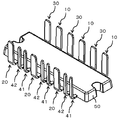
- FIG. 1 is a perspective view of a semiconductor device according to an embodiment of the present invention as viewed from the surface side.
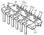
- FIG. 2 is a perspective view of the semiconductor device according to the embodiment of the present invention as seen from the back side.
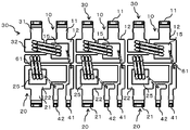
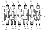
- FIG. 3 is an upper plan view showing a connection mode in the semiconductor device according to the first mode of the embodiment of the present invention.
- FIG. 4 is an upper plan view showing a connection mode in the semiconductor device according to the second mode of the embodiment of the present invention.
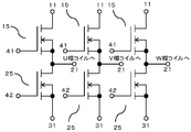
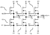
- FIG. 5 is a circuit diagram of the semiconductor device according to the first aspect of the embodiment of the present invention.
- FIG. 6 is a circuit diagram of the semiconductor device according to the second mode of the embodiment of the present invention.
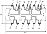
- FIG. 7 is a lower plan view showing the back surface of the semiconductor device according to the embodiment of the present invention.
- FIG. 8 is a side sectional view showing a state in which the semiconductor device according to the embodiment of the present invention is placed in the recess of the housing.
- FIG. 9 is an upper plan view showing a connection mode in a semiconductor device according to a modified example (mode using a connector) of the first mode of the embodiment of the present invention.
- FIG. 10 is an upper plan view showing a connection mode in a semiconductor device according to a modified example (mode using a connector) of the second mode of the embodiment of the present invention.
- the semiconductor device includes a plurality of first conductor portions 10, a plurality of second conductor portions 20, and upper surfaces of the first conductor portions 10 and the second conductor portions 20. And a sealing portion 50 for covering.
- the first conductor portion 10 includes a first terminal 11, a first main body portion 12 integrated with the first terminal 11, and a first body portion 12 provided on the first main body portion 12.
- the second conductor part 20 includes a second terminal 21, a second main body part 22 integrated with the second terminal 21, and a second electronic element 25 provided on the second main body part 22. Yes.
- the 1st main-body part 12 and the 2nd main-body part 22 consist of copper alloys etc., for example, and the tin plating process, the nickel plating process, etc. may be given to the whole surface or part.
- An epoxy resin or the like may be used as the sealing unit 50.
- a power semiconductor device may be used as the semiconductor device of the present embodiment.
- a MOSFET may be used as the first electronic element 15 and the second electronic element 25 for example.
- Circuit diagrams of the semiconductor device according to the present embodiment are as shown in FIGS. 5 and 6, for example. 5 and 6, the first electronic element 15 and the second electronic element 25 are MOSFETs.
- the drain of the MOSFET that is the first electronic element 15 is on the first body 12 side.
- the source is located on the opposite side of the first main body 12 (the front side of the paper in FIG. 3), and the drain of the MOSFET as the second electronic element 25 is on the second main body 22 side.
- the source is located on the side opposite to the second main body 22 (the front side in FIG. 3).
- the source of the MOSFET which is the first electronic element 15 is located on the first main body 12 side (the front side in FIG. 4), and the drain is on the opposite side of the first main body 12 (the paper in FIG. 4).
- the source of the MOSFET which is the second electronic element 25 is located on the second main body 22 side (the front side of the drawing in FIG. 4), and the drain is on the opposite side of the second main body 22 (the drawing of FIG. 4). Located on the back side.
- the first conductor portion 10 and the second conductor portion 20 are connected.
- the first conductor portion 10 and the second conductor portion 20 may be connected by a wire 61 as shown in FIGS. 3 and 4, or may be connected by a connector 62 as shown in FIGS. 9 and 10.
- the first electronic element 15 and the second main body 22 may be connected by a wire 61, or as shown in FIG.
- One body portion 12 may be connected by a wire 61.
- the first electronic element 15 and the second main body 22 may be connected by a connector 62, or as shown in FIG. 10, the second electronic element 25 and the first main body 12 May be connected by a connector 62.
- the connector 62 for example, a copper clip can be used, and as the wire 61, for example, an aluminum wire can be used. Note that the amount of current flowing can be increased by using the connector 62.
- the second terminal 21 is an output terminal (see FIG. 5), and when the second terminal 21 is used as a power supply terminal, the first terminal 11 is an output terminal (see FIG. 5). 6), the usage mode of the first terminal 11 and the second terminal 21 can be selected.
- the back surfaces of the first conductor portion 10 and the second conductor portion 20 may be exposed from the sealing portion 50. Under the present circumstances, although the back surface of the 1st conductor part 10 and the 2nd conductor part 20 may be partially exposed from the sealing part 50, as shown in FIG.2 and FIG.7, you may expose completely.
- the first conductor portion 10 and the second conductor portion 20 exposed in this manner may be placed on the housing 95 via a heat dissipation sheet 90, a heat dissipation adhesive, or the like, as shown in FIG. .
- “back surface” means the side shown in FIG. 7, and “front surface” means the opposite side to “back surface”.
- the first main body 12 and the second main body 22 may be substantially L-shaped when viewed from the back side.
- the “substantially L-shaped” means a portion extending in the vertical direction in FIG. 7 (hereinafter also referred to as “vertical bar portion”) and a portion extending in the left-right direction in FIG. .) May exist, corners may be rounded, or small protrusions may be provided.
- each of the plurality of first main body portions 12 may have the same shape when viewed from the back surface.
- each of the plurality of second main body portions 22 may have the same shape.
- each of the plurality of first main body portions 12 and the plurality of second main body portions 22 may have the same shape.
- the area of the first main body portion 12 exposed from the sealing portion 50 and the area of the second main body portion 22 exposed from the sealing portion 50 are It may be substantially the same. Further, in this case, when viewed from the back surface side, the area of the portion exposed from the back surface of the sealing portion 50 with respect to the first terminal 11 and the first body portion 12, and the second terminal 21 and the second body. The area of the portion exposed from the back surface of the sealing portion 50 with respect to the portion 22 may be substantially the same. In the present embodiment, the “area” is “substantially the same” means that the area is within ⁇ 10% of the entire area.
- the portion exposed from the back surface of the first main body portion 12 When the area is “A1” and the area of the portion exposed from the back surface of the second main body portion 22 is “A2”, A2 ⁇ 0.9 ⁇ A1 ⁇ A2 ⁇ 1.1. means.
- the area A1 of the portion exposed from the back surface of the first main body portion 12 is larger than the area A2 of the portion exposed from the back surface of the second main body portion 22.
- the semiconductor device according to the present embodiment further includes a third conductor portion 30 having a third terminal 31 and a third main body portion 32 integrated with the third terminal 31. You may have.
- the third conductor portion 30 may be directly connected to the first electronic element 15 as shown in FIGS. 4 and 10 or directly connected to the second electronic element 25 as shown in FIGS. 3 and 9. May be.
- the third terminal 31 may be a ground terminal.
- the first terminal 11 is used as an input terminal by connecting the first electronic element 15 to the second body 22 and connecting the second electronic element 25 to the third terminal 31.
- the second terminal 21 can be used as an output terminal
- the third terminal 31 can be used as a ground terminal (see FIG. 5).
- the second electronic element 25 is connected to the first main body portion 12, and the first electronic element 15 is connected to the third terminal 31, whereby the second terminal 21 is connected to the input terminal.
- the first terminal 11 can be used as an output terminal
- the third terminal 31 can be used as a ground terminal (see FIG. 6).
- the semiconductor device of the present embodiment may have control terminals 41 and 42.
- two control terminals 41 and 42 are used, and each control terminal 41 and 42 is connected to the electronic elements 15 and 16. That is, the first control terminal 41 is connected to the first electronic element 15 by the wire 61 and is used to control the first electronic element 15.
- the second control terminal 42 is connected to the second electronic element 25 with a wire 61 and is used to control the second electronic element 25.
- each of the first terminal 11, the second terminal 21, and the third terminal 31 may be bent to the surface side (sealing portion 50 side).
- the height H of the terminal when bent is, for example, 5 to 15 mm (typically about 10 mm), and the thickness D1 of the sealing portion 50 is 2 to 5 mm (typically 3.5 mm).
- the thickness D2 of each terminal is 0.3 to 0.9 mm (typically about 0.6 mm).
- the length L1 (see FIG. 7) in the longitudinal direction of the semiconductor device is 40 mm to 50 mm (typically 44 mm), and the length in the short direction of the semiconductor device (the length between the bent portions of the terminals) L2 is 15 mm. ⁇ 25 mm (typically 20 mm).
- the first terminal 11 is not bent, the first main body 12, the second terminal 21 is not bent, the second main body 22, and the third terminal 31 is bent.
- the part which is not bent, the third main body 32, the part where the first control terminal 41 is not bent and the part where the second control terminal 42 is not bent are flush with each other. For this reason, as described above, when the semiconductor device is placed on the heat dissipation sheet 90 (see FIG. 8), all of these can be brought into contact with the heat dissipation sheet 90.
- the first body 12 the second terminal 21 is not bent, the second body 22, the third terminal 31 is not bent, the third body 32, when the unbent portion of the first control terminal 41 and the unbent portion of the second control terminal 42 are completely exposed, all of them can be brought into contact with the heat dissipation sheet 90. This is advantageous in that a higher heat dissipation effect can be realized.
- the semiconductor device of this embodiment may be a three-phase bridge circuit.
- One of the three output terminals may be connected to the U-phase coil, another one may be connected to the V-phase coil, and the remaining one may be connected to the W-phase coil.
- the drain of the MOSFET that is the first electronic element 15 is connected to the power supply line side
- the source is connected to the drain of the MOSFET that is the second electronic element 25
- the source of this MOSFET is the ground. It is connected to the.
- the connection point of the 1st electronic element 15 and the 2nd electronic element 25 is connected to the U phase coil of the motor, the V phase coil, or the W phase coil.
- the drain of the MOSFET that is the second electronic element 25 is connected to the power supply line side, the source is connected to the drain of the MOSFET that is the first electronic element 15, and the source of the MOSFET is connected to the ground. Yes.
- a connection point between the second electronic element 25 and the first electronic element 15 is connected to a U-phase coil, a V-phase coil, or a W-phase coil of the motor.
- the connection mode between the first conductor portion 10 and the second conductor portion 20 when the first terminal 11 is used as a power supply terminal, the second terminal 21 becomes an output terminal (see FIG. 5), when the second terminal 21 is used as a power supply terminal, the first terminal 11 becomes an output terminal (see FIG. 6), and the usage mode of the first terminal 11 and the second terminal 21 can be selected. Yes. For this reason, a terminal functioning as a power supply terminal and a terminal functioning as an output terminal can be appropriately selected.
- a terminal functioning as a power supply terminal and a terminal functioning as an output terminal can be appropriately selected, assembly of the entire device such as a controller including a semiconductor device can be facilitated, and productivity can be improved.
- the semiconductor device of this Embodiment is a power module, it will be connected with a control module. Since a terminal functioning as a power supply terminal and a terminal functioning as an output terminal can be appropriately selected as in the present embodiment, the degree of freedom of patterning of the control module can be increased.
- the manufacturing cost can be reduced.
- the manufacturing cost can be further reduced.
- first conductor portion 10 and the second conductor portion 20 are exposed (particularly completely) as described above, a plurality of first conductors are used in order to prevent the sealing portion 50 from coming out. It is more advantageous that the first conductor portion 10 or the second conductor portion 20 is not integrated with the portion 10 or the plurality of second conductor portions 20, but is integrated. However, in the present embodiment, each of the first conductor portion 10 and the second conductor portion 20 is not separated into an integral shape, but is individually separated. With such a separated aspect, as described above, a terminal functioning as a power supply terminal and a terminal functioning as an output terminal can be appropriately selected.
- the lead frame is only connected by a tie bar before cutting, and the first conductor portion 10, the second conductor portion 20, the third conductor portion 30, the first control terminal 41, and the first control terminal 41 are connected.
- Each of the two control terminals 42 is basically a disjoint member.
- the configuration in which the first conductor portion 10 is integrated or the configuration in which the second conductor portion 20 is integrated may be affected by high frequencies or the like (noise or the like) in other phases.
- high frequencies or the like noise or the like
- by adopting a mode in which each first conductor portion 10 and each second conductor portion 20 are separated as in the present embodiment it is less likely to be affected by high frequencies (noise, etc.) in other phases. It is also beneficial in that it can.
- the plurality of electronic elements 15 and 25 can be evenly radiated by arranging them evenly.
- the electronic elements 15 and 25 can be mounted quickly, and productivity can be increased.
- “Equal” in the present embodiment means that the distance between the plurality of first electronic elements 15 has the same value, the distance between the plurality of second electronic elements 25 has the same value, and the longitudinal direction of the semiconductor device (FIG.
- a plurality of first electronic elements 15 are arranged on one side (upper side in FIGS. 3 and 4) from the center line extending in the horizontal direction 3 and FIG. 4 and on the other side (lower side in FIGS. 3 and 4).
- a plurality of second electronic elements 25 are arranged, and the first electronic element 15 and the second electronic element 25 are nested.
- first electronic elements 15 are arranged at equal intervals in the left-right direction above the center line in the longitudinal direction of the semiconductor device in FIGS. 3 and 4.
- second electronic elements 25 are arranged at equal intervals in the left-right direction below the center line in the longitudinal direction in FIGS. This means that the electronic element 15 and the second electronic element 25 are arranged in a nested state.
- the wire 61 when the wire 61 is employed, it is beneficial in that the wires 61 can be efficiently connected by arranging the plurality of electronic elements 15 and 25 evenly. It is.
- the connector 62 such as a clip
- the types of the connector 62 to be prepared are reduced. Can do.
- the length of the child 62 can be made substantially the same.
- the length can be approximately the same length.
- the type of the connector 62 prepared in advance can be made one. Further, it is also advantageous in that the amount of current flowing through each connector 62 can be made substantially the same value by using one type of connector 62 to be used.
- first main body 12 and the second main body 22 are configured so as to have a substantially L shape when viewed from the back side
- other terminals can be provided in a substantially L-shaped blank portion.
- the third terminal 31 can be provided on the left side of the vertical bar portion of the first main body portion 12, and the vertical bar portion of the second main body portion 22.
- a second control terminal 42 can be provided on the right side of the second control terminal 42.
- the length of the horizontal bar portion of the second main body portion 22 is shorter than the length of the horizontal bar portion of the first main body portion 12,
- the first control terminal 41 can also be provided on the right side of the second main body 22.
- the 1st terminal 11 and the 2nd terminal 21 it is advantageous in that it can have the same electrical characteristics and can be combined with the heat dissipation characteristics. That is, when the first terminal 11 functions as a power supply terminal and the second terminal 21 functions as an output terminal, and when the first terminal 11 functions as an output terminal and the second terminal 21 functions as a power supply terminal. Are advantageous in that they can have the same electrical characteristics and heat dissipation characteristics.
- the first electronic element 15 is connected to the second main body portion 22, and the second electronic element 25 is connected to the third terminal 31, thereby inputting the first terminal 11.
- the second terminal 21 can be used as an output terminal, and the third terminal 31 can be used as a ground terminal.
- the second electronic element 25 is connected to the first main body portion 12, and the first electronic element 15 is connected to the third terminal 31, whereby the second terminal 21 is connected to the input terminal.
- the first terminal 11 can be used as an output terminal
- the third terminal 31 can be used as a ground terminal. Therefore, in any case, the current input from one side of the semiconductor device in the short direction (the upper side in FIG. 3 and the lower side in FIG.
Landscapes
- Inverter Devices (AREA)
- Engineering & Computer Science (AREA)
- Microelectronics & Electronic Packaging (AREA)
- Lead Frames For Integrated Circuits (AREA)
- Structures Or Materials For Encapsulating Or Coating Semiconductor Devices Or Solid State Devices (AREA)
Abstract
Description
第一端子と、前記第一端子と一体になった第一本体部と、前記第一本体部上に設けられた第一電子素子と、を有する複数の第一導体部と、
第二端子と、前記第二端子と一体になった第二本体部と、前記第二本体部上に設けられた第二電子素子と、を有する複数の第二導体部と、
前記第一導体部及び前記第二導体部の上面を覆う封止部と、
を備え、
前記第一導体部と前記第二導体部とが接続され、
前記第一導体部と前記第二導体部の接続態様を変えることで、前記第一端子を電源端子として利用する場合には前記第二端子が出力端子となり、前記第二端子を電源端子として利用する場合には前記第一端子が出力端子となるよう、前記第一端子及び前記第二端子の利用態様を選択できる。
前記第一導体部及び前記第二導体部の裏面は前記封止部から露出してもよい。
前記第一本体部及び前記第二本体部は裏面側から見たときに略L字形状となってもよい。
裏面側から見たときに複数の前記第一本体部の各々は同じ形状であり、
裏面側から見たときに複数の前記第二本体部の各々は同じ形状であってもよい。
裏面側から見たときに、前記第一本体部の前記封止部から露出している部分の面積と、前記第二本体部の前記封止部から露出している部分の面積とは略同一であってもよい。
前記第一電子素子と前記第二本体部とは接続子で接続される、又は、前記第二電子素子と前記第一本体部とは接続子で接続されてもよい。
複数の前記接続子の長さが同一であってもよい。
第三端子と、前記第三端子と一体になった第三本体部と、を有する第三導体部をさらに備え、
前記第三導体部は、前記第一電子素子又は前記第二電源素子と直接接続されてもよい。
前記第三端子はグランド端子であってもよい。
前記第一端子及び前記第二端子は表面側に屈曲されており、
前記第一本体部、前記第二本体部、前記第一端子の屈曲されていない部分及び第二端子の屈曲されていない部分は裏面側で面一となってもよい。
表面側から見たときに複数の前記第一電子素子及び複数の前記第二電子素子が均等に配列されてもよい。
《構成》
図1及び図2に示すように、本実施の形態の半導体装置は、複数の第一導体部10と、複数の第二導体部20と、第一導体部10及び第二導体部20の上面を覆う封止部50と、を有している。図3及び図4に示すように、第一導体部10は、第一端子11と、第一端子11と一体になった第一本体部12と、第一本体部12上に設けられた第一電子素子15と、を有している。第二導体部20は、第二端子21と、第二端子21と一体になった第二本体部22と、第二本体部22上に設けられた第二電子素子25と、を有している。第一本体部12及び第二本体部22は、例えば、銅合金等からなり、全面又は部分的にスズめっき処理やニッケルめっき処理等が施されていてもよい。封止部50としてはエポキシ樹脂等を用いてもよい。
次に、上述した構成からなる本実施の形態による作用・効果のうち、まだ説明していないものについて説明する。なお、「作用・効果」で説明するあらゆる態様を、上記構成で採用することができる。
11 第一端子
12 第一本体部
15 第一電子素子
20 第二導体部
21 第二端子
22 第二本体部
25 第二電子素子
30 第三導体部
31 第三端子
32 第三本体部
50 封止部
61 ワイヤ
62 接続子
Claims (11)
- 第一端子と、前記第一端子と一体になった第一本体部と、前記第一本体部上に設けられた第一電子素子と、を有する複数の第一導体部と、
第二端子と、前記第二端子と一体になった第二本体部と、前記第二本体部上に設けられた第二電子素子と、を有する複数の第二導体部と、
前記第一導体部及び前記第二導体部の上面を覆う封止部と、
を備え、
前記第一導体部と前記第二導体部とは接続され、
前記第一導体部と前記第二導体部の接続態様を変えることで、前記第一端子を電源端子として利用する場合には前記第二端子が出力端子となり、前記第二端子を電源端子として利用する場合には前記第一端子が出力端子となるよう、前記第一端子及び前記第二端子の利用態様を選択できることを特徴とする半導体装置。 - 前記第一導体部及び前記第二導体部の裏面は前記封止部から露出していることを特徴とする請求項1に記載の半導体装置。
- 前記第一本体部及び前記第二本体部は裏面側から見たときに略L字形状となることを特徴とする請求項1又は2のいずれかに記載の半導体装置。
- 裏面側から見たときに複数の前記第一本体部の各々は同じ形状であり、
裏面側から見たときに複数の前記第二本体部の各々は同じ形状であることを特徴とする請求項1乃至3のいずれか1項に記載の半導体装置。 - 裏面側から見たときに、前記第一本体部の前記封止部から露出している部分の面積と、前記第二本体部の前記封止部から露出している部分の面積とは略同一であることを特徴とする請求項1乃至4のいずれか1項に記載の半導体装置。
- 前記第一電子素子と前記第二本体部とは接続子で接続される、又は、前記第二電子素子と前記第一本体部とは接続子で接続されることを特徴とすることを特徴とする請求項1乃至5のいずれか1項に記載の半導体装置。
- 複数の前記接続子の長さが同一であることを特徴とすることを特徴とする請求項6に記載の半導体装置。
- 第三端子と、前記第三端子と一体になった第三本体部と、を有する第三導体部をさらに備え、
前記第三導体部は、前記第一電子素子又は前記第二電源素子と直接接続されることを特徴とする請求項1乃至7のいずれか1項に記載の半導体装置。 - 前記第三端子はグランド端子であることを特徴とする請求項8に記載の半導体装置。
- 前記第一端子及び前記第二端子は表面側に屈曲されており、
前記第一本体部、前記第二本体部、前記第一端子の屈曲されていない部分及び第二端子の屈曲されていない部分は裏面側で面一となっていることを特徴とする請求項1乃至9のいずれか1項に記載の半導体装置。 - 表面側から見たときに複数の前記第一電子素子及び複数の前記第二電子素子が均等に配列されていることを特徴とする請求項1乃至10のいずれか1項に記載の半導体装置。
Priority Applications (5)
| Application Number | Priority Date | Filing Date | Title |
|---|---|---|---|
| PCT/JP2016/057712 WO2017154189A1 (ja) | 2016-03-11 | 2016-03-11 | 半導体装置 |
| US15/513,396 US10453781B2 (en) | 2016-03-11 | 2016-03-11 | Semiconductor device |
| CN201680003084.1A CN107408553B (zh) | 2016-03-11 | 2016-03-11 | 半导体装置 |
| JP2016571441A JP6255116B1 (ja) | 2016-03-11 | 2016-03-11 | 半導体装置 |
| NL2018505A NL2018505B1 (en) | 2016-03-11 | 2017-03-13 | Semiconductor device |
Applications Claiming Priority (1)
| Application Number | Priority Date | Filing Date | Title |
|---|---|---|---|
| PCT/JP2016/057712 WO2017154189A1 (ja) | 2016-03-11 | 2016-03-11 | 半導体装置 |
Publications (1)
| Publication Number | Publication Date |
|---|---|
| WO2017154189A1 true WO2017154189A1 (ja) | 2017-09-14 |
Family
ID=58737817
Family Applications (1)
| Application Number | Title | Priority Date | Filing Date |
|---|---|---|---|
| PCT/JP2016/057712 Ceased WO2017154189A1 (ja) | 2016-03-11 | 2016-03-11 | 半導体装置 |
Country Status (5)
| Country | Link |
|---|---|
| US (1) | US10453781B2 (ja) |
| JP (1) | JP6255116B1 (ja) |
| CN (1) | CN107408553B (ja) |
| NL (1) | NL2018505B1 (ja) |
| WO (1) | WO2017154189A1 (ja) |
Cited By (2)
| Publication number | Priority date | Publication date | Assignee | Title |
|---|---|---|---|---|
| NL2021929A (en) * | 2017-11-10 | 2019-05-15 | Shindengen Electric Mfg | Electronic module and method of manufacturing the same |
| EP3787019A4 (en) * | 2018-04-25 | 2021-05-05 | Mitsubishi Electric Corporation | Shared base plate and semiconductor module provided with same |
Citations (3)
| Publication number | Priority date | Publication date | Assignee | Title |
|---|---|---|---|---|
| US20070267742A1 (en) * | 2006-05-19 | 2007-11-22 | Liang-Pin Tai | Dual mosfet package |
| US20130032855A1 (en) * | 2011-08-05 | 2013-02-07 | Infineon Technologies Ag | Semiconductor Arrangement |
| JP2014029944A (ja) * | 2012-07-31 | 2014-02-13 | Aisin Aw Co Ltd | スイッチング素子ユニット |
Family Cites Families (10)
| Publication number | Priority date | Publication date | Assignee | Title |
|---|---|---|---|---|
| JP2008118067A (ja) * | 2006-11-08 | 2008-05-22 | Hitachi Ltd | パワーモジュール及びモータ一体型コントロール装置 |
| US8456141B2 (en) * | 2007-06-11 | 2013-06-04 | Alpha & Omega Semiconductor, Inc. | Boost converter with integrated high power discrete FET and low voltage controller |
| JP2010199492A (ja) * | 2009-02-27 | 2010-09-09 | Sanyo Electric Co Ltd | 半導体装置およびその製造方法 |
| JP5099243B2 (ja) * | 2010-04-14 | 2012-12-19 | 株式会社デンソー | 半導体モジュール |
| JP5067679B2 (ja) | 2010-05-21 | 2012-11-07 | 株式会社デンソー | 半導体モジュール、および、それを用いた駆動装置 |
| WO2012108011A1 (ja) * | 2011-02-09 | 2012-08-16 | 三菱電機株式会社 | パワー半導体モジュール |
| JP5569555B2 (ja) * | 2012-05-17 | 2014-08-13 | 株式会社デンソー | 配線部材、および、これを用いた半導体モジュール |
| JP5879233B2 (ja) * | 2012-08-31 | 2016-03-08 | 日立オートモティブシステムズ株式会社 | パワー半導体モジュール |
| ITTO20121081A1 (it) * | 2012-12-14 | 2014-06-15 | St Microelectronics Srl | Componente elettronico di potenza normalmente spento |
| JP6020379B2 (ja) * | 2013-08-02 | 2016-11-02 | 株式会社デンソー | 半導体装置 |
-
2016
- 2016-03-11 WO PCT/JP2016/057712 patent/WO2017154189A1/ja not_active Ceased
- 2016-03-11 CN CN201680003084.1A patent/CN107408553B/zh active Active
- 2016-03-11 US US15/513,396 patent/US10453781B2/en active Active
- 2016-03-11 JP JP2016571441A patent/JP6255116B1/ja active Active
-
2017
- 2017-03-13 NL NL2018505A patent/NL2018505B1/en active
Patent Citations (3)
| Publication number | Priority date | Publication date | Assignee | Title |
|---|---|---|---|---|
| US20070267742A1 (en) * | 2006-05-19 | 2007-11-22 | Liang-Pin Tai | Dual mosfet package |
| US20130032855A1 (en) * | 2011-08-05 | 2013-02-07 | Infineon Technologies Ag | Semiconductor Arrangement |
| JP2014029944A (ja) * | 2012-07-31 | 2014-02-13 | Aisin Aw Co Ltd | スイッチング素子ユニット |
Cited By (3)
| Publication number | Priority date | Publication date | Assignee | Title |
|---|---|---|---|---|
| NL2021929A (en) * | 2017-11-10 | 2019-05-15 | Shindengen Electric Mfg | Electronic module and method of manufacturing the same |
| US11227816B2 (en) | 2017-11-10 | 2022-01-18 | Shindengen Electric Manufacturing Co., Ltd. | Electronic module with press hole to expose surface of a conductor |
| EP3787019A4 (en) * | 2018-04-25 | 2021-05-05 | Mitsubishi Electric Corporation | Shared base plate and semiconductor module provided with same |
Also Published As
| Publication number | Publication date |
|---|---|
| NL2018505A (en) | 2017-09-20 |
| CN107408553A (zh) | 2017-11-28 |
| NL2018505B1 (en) | 2017-12-20 |
| US10453781B2 (en) | 2019-10-22 |
| JPWO2017154189A1 (ja) | 2018-03-15 |
| US20180233437A1 (en) | 2018-08-16 |
| JP6255116B1 (ja) | 2017-12-27 |
| CN107408553B (zh) | 2019-07-26 |
Similar Documents
| Publication | Publication Date | Title |
|---|---|---|
| CN107004649B (zh) | 电子部件搭载用散热基板 | |
| JP6160780B2 (ja) | 3レベル電力変換装置 | |
| CN105580263B (zh) | 电力转换装置 | |
| US9640470B2 (en) | Semiconductor module | |
| CN107004648A (zh) | 电子部件搭载用散热基板 | |
| WO2015068565A1 (ja) | 半導体装置 | |
| JP6560819B1 (ja) | 電子モジュール及び電子モジュールの製造方法 | |
| JP2013507760A (ja) | 自動車のための電力モジュール | |
| JP6123722B2 (ja) | 半導体装置 | |
| JP6255116B1 (ja) | 半導体装置 | |
| JP6357596B1 (ja) | 電子モジュール | |
| JP2010192240A (ja) | 半導体リレーモジュール付ワイヤハーネス | |
| JP6179487B2 (ja) | 3レベル電力変換装置の半導体モジュールユニット | |
| JP6402280B2 (ja) | 電子機器 | |
| US11227810B2 (en) | Electronic module with a groove and press hole on the surface of a conductor | |
| JP7031452B2 (ja) | コンデンサ | |
| CN107431066A (zh) | 半导体装置 | |
| NL2020161B1 (en) | Electronic module | |
| JP4745925B2 (ja) | 自動車用モータの制御用コネクタ一体型半導体モジュール | |
| JP6510146B1 (ja) | 電子モジュール | |
| WO2018042659A1 (ja) | 電子機器 |
Legal Events
| Date | Code | Title | Description |
|---|---|---|---|
| ENP | Entry into the national phase |
Ref document number: 2016571441 Country of ref document: JP Kind code of ref document: A |
|
| WWE | Wipo information: entry into national phase |
Ref document number: 15513396 Country of ref document: US |
|
| NENP | Non-entry into the national phase |
Ref country code: DE |
|
| 121 | Ep: the epo has been informed by wipo that ep was designated in this application |
Ref document number: 16893516 Country of ref document: EP Kind code of ref document: A1 |
|
| 122 | Ep: pct application non-entry in european phase |
Ref document number: 16893516 Country of ref document: EP Kind code of ref document: A1 |