WO2017150361A1 - 樹脂基板 - Google Patents
樹脂基板 Download PDFInfo
- Publication number
- WO2017150361A1 WO2017150361A1 PCT/JP2017/007010 JP2017007010W WO2017150361A1 WO 2017150361 A1 WO2017150361 A1 WO 2017150361A1 JP 2017007010 W JP2017007010 W JP 2017007010W WO 2017150361 A1 WO2017150361 A1 WO 2017150361A1
- Authority
- WO
- WIPO (PCT)
- Prior art keywords
- resin
- conductor
- resin substrate
- interlayer connection
- conductor pattern
- Prior art date
- Legal status (The legal status is an assumption and is not a legal conclusion. Google has not performed a legal analysis and makes no representation as to the accuracy of the status listed.)
- Ceased
Links
Images


Classifications
-
- H—ELECTRICITY
- H05—ELECTRIC TECHNIQUES NOT OTHERWISE PROVIDED FOR
- H05K—PRINTED CIRCUITS; CASINGS OR CONSTRUCTIONAL DETAILS OF ELECTRIC APPARATUS; MANUFACTURE OF ASSEMBLAGES OF ELECTRICAL COMPONENTS
- H05K1/00—Printed circuits
- H05K1/02—Details
- H05K1/0271—Arrangements for reducing stress or warp in rigid printed circuit boards, e.g. caused by loads, vibrations or differences in thermal expansion
-
- H—ELECTRICITY
- H05—ELECTRIC TECHNIQUES NOT OTHERWISE PROVIDED FOR
- H05K—PRINTED CIRCUITS; CASINGS OR CONSTRUCTIONAL DETAILS OF ELECTRIC APPARATUS; MANUFACTURE OF ASSEMBLAGES OF ELECTRICAL COMPONENTS
- H05K3/00—Apparatus or processes for manufacturing printed circuits
- H05K3/40—Forming printed elements for providing electric connections to or between printed circuits
- H05K3/4038—Through-connections; Vertical interconnect access [VIA] connections
- H05K3/4053—Through-connections; Vertical interconnect access [VIA] connections by thick-film techniques
- H05K3/4069—Through-connections; Vertical interconnect access [VIA] connections by thick-film techniques for via connections in organic insulating substrates
-
- H—ELECTRICITY
- H05—ELECTRIC TECHNIQUES NOT OTHERWISE PROVIDED FOR
- H05K—PRINTED CIRCUITS; CASINGS OR CONSTRUCTIONAL DETAILS OF ELECTRIC APPARATUS; MANUFACTURE OF ASSEMBLAGES OF ELECTRICAL COMPONENTS
- H05K1/00—Printed circuits
- H05K1/02—Details
- H05K1/03—Use of materials for the substrate
- H05K1/0313—Organic insulating material
-
- H—ELECTRICITY
- H05—ELECTRIC TECHNIQUES NOT OTHERWISE PROVIDED FOR
- H05K—PRINTED CIRCUITS; CASINGS OR CONSTRUCTIONAL DETAILS OF ELECTRIC APPARATUS; MANUFACTURE OF ASSEMBLAGES OF ELECTRICAL COMPONENTS
- H05K1/00—Printed circuits
- H05K1/02—Details
- H05K1/09—Use of materials for the conductive, e.g. metallic pattern
- H05K1/092—Dispersed materials, e.g. conductive pastes or inks
-
- H—ELECTRICITY
- H05—ELECTRIC TECHNIQUES NOT OTHERWISE PROVIDED FOR
- H05K—PRINTED CIRCUITS; CASINGS OR CONSTRUCTIONAL DETAILS OF ELECTRIC APPARATUS; MANUFACTURE OF ASSEMBLAGES OF ELECTRICAL COMPONENTS
- H05K1/00—Printed circuits
- H05K1/02—Details
- H05K1/11—Printed elements for providing electric connections to or between printed circuits
- H05K1/115—Via connections; Lands around holes or via connections
-
- H—ELECTRICITY
- H05—ELECTRIC TECHNIQUES NOT OTHERWISE PROVIDED FOR
- H05K—PRINTED CIRCUITS; CASINGS OR CONSTRUCTIONAL DETAILS OF ELECTRIC APPARATUS; MANUFACTURE OF ASSEMBLAGES OF ELECTRICAL COMPONENTS
- H05K3/00—Apparatus or processes for manufacturing printed circuits
- H05K3/0011—Working of insulating substrates or insulating layers
-
- H—ELECTRICITY
- H05—ELECTRIC TECHNIQUES NOT OTHERWISE PROVIDED FOR
- H05K—PRINTED CIRCUITS; CASINGS OR CONSTRUCTIONAL DETAILS OF ELECTRIC APPARATUS; MANUFACTURE OF ASSEMBLAGES OF ELECTRICAL COMPONENTS
- H05K3/00—Apparatus or processes for manufacturing printed circuits
- H05K3/40—Forming printed elements for providing electric connections to or between printed circuits
- H05K3/4038—Through-connections; Vertical interconnect access [VIA] connections
-
- H—ELECTRICITY
- H05—ELECTRIC TECHNIQUES NOT OTHERWISE PROVIDED FOR
- H05K—PRINTED CIRCUITS; CASINGS OR CONSTRUCTIONAL DETAILS OF ELECTRIC APPARATUS; MANUFACTURE OF ASSEMBLAGES OF ELECTRICAL COMPONENTS
- H05K3/00—Apparatus or processes for manufacturing printed circuits
- H05K3/46—Manufacturing multilayer circuits
-
- H—ELECTRICITY
- H05—ELECTRIC TECHNIQUES NOT OTHERWISE PROVIDED FOR
- H05K—PRINTED CIRCUITS; CASINGS OR CONSTRUCTIONAL DETAILS OF ELECTRIC APPARATUS; MANUFACTURE OF ASSEMBLAGES OF ELECTRICAL COMPONENTS
- H05K3/00—Apparatus or processes for manufacturing printed circuits
- H05K3/46—Manufacturing multilayer circuits
- H05K3/4611—Manufacturing multilayer circuits by laminating two or more circuit boards
- H05K3/4614—Manufacturing multilayer circuits by laminating two or more circuit boards the electrical connections between the circuit boards being made during lamination
- H05K3/4617—Manufacturing multilayer circuits by laminating two or more circuit boards the electrical connections between the circuit boards being made during lamination characterized by laminating only or mainly similar single-sided circuit boards
-
- H—ELECTRICITY
- H05—ELECTRIC TECHNIQUES NOT OTHERWISE PROVIDED FOR
- H05K—PRINTED CIRCUITS; CASINGS OR CONSTRUCTIONAL DETAILS OF ELECTRIC APPARATUS; MANUFACTURE OF ASSEMBLAGES OF ELECTRICAL COMPONENTS
- H05K3/00—Apparatus or processes for manufacturing printed circuits
- H05K3/46—Manufacturing multilayer circuits
- H05K3/4644—Manufacturing multilayer circuits by building the multilayer layer by layer, i.e. build-up multilayer circuits
-
- H—ELECTRICITY
- H05—ELECTRIC TECHNIQUES NOT OTHERWISE PROVIDED FOR
- H05K—PRINTED CIRCUITS; CASINGS OR CONSTRUCTIONAL DETAILS OF ELECTRIC APPARATUS; MANUFACTURE OF ASSEMBLAGES OF ELECTRICAL COMPONENTS
- H05K3/00—Apparatus or processes for manufacturing printed circuits
- H05K3/46—Manufacturing multilayer circuits
- H05K3/4688—Composite multilayer circuits, i.e. comprising insulating layers having different properties
- H05K3/4694—Partitioned multilayer circuits having adjacent regions with different properties, e.g. by adding or inserting locally circuit layers having a higher circuit density
-
- H—ELECTRICITY
- H05—ELECTRIC TECHNIQUES NOT OTHERWISE PROVIDED FOR
- H05K—PRINTED CIRCUITS; CASINGS OR CONSTRUCTIONAL DETAILS OF ELECTRIC APPARATUS; MANUFACTURE OF ASSEMBLAGES OF ELECTRICAL COMPONENTS
- H05K2201/00—Indexing scheme relating to printed circuits covered by H05K1/00
- H05K2201/03—Conductive materials
- H05K2201/0332—Structure of the conductor
- H05K2201/0388—Other aspects of conductors
- H05K2201/0391—Using different types of conductors
-
- H—ELECTRICITY
- H05—ELECTRIC TECHNIQUES NOT OTHERWISE PROVIDED FOR
- H05K—PRINTED CIRCUITS; CASINGS OR CONSTRUCTIONAL DETAILS OF ELECTRIC APPARATUS; MANUFACTURE OF ASSEMBLAGES OF ELECTRICAL COMPONENTS
- H05K2201/00—Indexing scheme relating to printed circuits covered by H05K1/00
- H05K2201/06—Thermal details
- H05K2201/068—Thermal details wherein the coefficient of thermal expansion is important
-
- H—ELECTRICITY
- H05—ELECTRIC TECHNIQUES NOT OTHERWISE PROVIDED FOR
- H05K—PRINTED CIRCUITS; CASINGS OR CONSTRUCTIONAL DETAILS OF ELECTRIC APPARATUS; MANUFACTURE OF ASSEMBLAGES OF ELECTRICAL COMPONENTS
- H05K2201/00—Indexing scheme relating to printed circuits covered by H05K1/00
- H05K2201/09—Shape and layout
- H05K2201/09209—Shape and layout details of conductors
- H05K2201/095—Conductive through-holes or vias
-
- H—ELECTRICITY
- H05—ELECTRIC TECHNIQUES NOT OTHERWISE PROVIDED FOR
- H05K—PRINTED CIRCUITS; CASINGS OR CONSTRUCTIONAL DETAILS OF ELECTRIC APPARATUS; MANUFACTURE OF ASSEMBLAGES OF ELECTRICAL COMPONENTS
- H05K2201/00—Indexing scheme relating to printed circuits covered by H05K1/00
- H05K2201/09—Shape and layout
- H05K2201/09818—Shape or layout details not covered by a single group of H05K2201/09009 - H05K2201/09809
- H05K2201/09827—Tapered, e.g. tapered hole, via or groove
Definitions
- the present invention relates to a resin substrate on which a plurality of resin sheets are laminated.
- the resin substrate of Patent Document 1 is formed by laminating a plurality of resin sheets. Conductive patterns are formed on the plurality of resin sheets. With this configuration, the conductor pattern is arranged in a plurality of layers of the resin substrate.
- Conductor patterns arranged in different layers are connected by interlayer connection conductors.
- the conductor patterns of the plurality of layers are conductive.
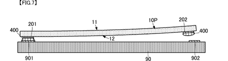
- FIG. 7 is a side view for explaining the problem of the conventional resin substrate.
- the resin substrate 10P is a flat plate having a long outer shape.
- External connection conductors 201 and 202 are formed on the back surface 12 of the resin substrate 10P.
- the external connection conductor 201 is formed at one end in the length direction.
- the external connection conductor 202 is formed at the other end in the length direction.
- the density of the conductor pattern in the plurality of layers on the front surface 11 side is lower than the density of the conductor pattern in the plurality of layers on the back surface 12 side.
- An object of the present invention is to provide a resin substrate capable of suppressing warpage due to thermal history or the like.
- the present invention relates to a long resin substrate including a plurality of resin sheets on which a planar conductor pattern is formed and on which a plurality of resin sheets including the resin sheets are laminated, and has the following characteristics.
- the resin substrate is constituted by a first portion constituted by a resin sheet closer to one end side than the other end in the laminating direction and a resin sheet closer to the other end side than one end in the laminating direction of the plurality of resin sheets.
- a second portion The density of the conductor pattern of the first part relative to the volume of the first part is lower than the density of the conductor pattern of the second part relative to the volume of the second part.
- the average diameter of the first interlayer connection conductor formed in the first portion is larger than the average diameter of the second interlayer connection conductor formed in the second portion.
- the density difference between the planar conductor pattern between the first part and the second part arranged in the thickness direction of the resin substrate is the difference between the diameter of the first interlayer connection conductor and the diameter of the second interlayer connection conductor. Mitigated by the difference.
- the resin substrate of the present invention preferably has the following configuration.
- the density with respect to the volume of the second part of the conductor pattern of the second part and the conductor of the second interlayer connection conductor based on the density of the conductor of the first part and the volume of the first part of the conductor made of the first interlayer connection conductor.
- the ratio is 0.5 or more and 1.0 or less.
- the plurality of resin sheets may be thermoplastic resins.
- the resin substrate is easily formed from a plurality of resin sheets.
- the resin substrate of the present invention may have a long outer shape extending in the longitudinal direction. In this configuration, the effect of suppressing the warpage of the configuration of the present invention is more effective.
- FIG. 1 is an exploded cross-sectional view of a resin substrate according to an embodiment of the present invention.
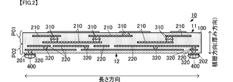
- FIG. 2 is a cross-sectional view of the resin substrate according to the embodiment of the present invention.
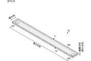
- FIG. 3 is an external perspective view of the resin substrate according to the embodiment of the present invention.
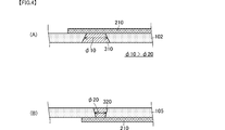
- 4A and 4B are enlarged cross-sectional views showing the shape of the interlayer connection conductor of the resin substrate according to the embodiment of the present invention. In FIGS. 1, 2, and 4, the thickness of the resin substrate is emphasized.
- the resin substrate 10 is a flat plate.
- the dimension in the length direction of the resin substrate 10 is significantly longer than the dimension in the width direction.
- the length direction of the resin substrate 10 is the longitudinal direction.
- the resin substrate 10 is a flat plate having a long outer shape.
- the configuration of the present embodiment is effective for a resin substrate having a length direction longer than a width direction and a dimension in the length direction being a predetermined value or more. For example, it is more effective when the dimension in the length direction is about twice or more than the dimension in the width direction.
- the resin substrate 10 includes a main body 100, external connection conductors 201 and 202, conductor patterns 210 and 220, and interlayer connection conductors 310 and 320.
- the external connection conductor 201 is formed at one end of the resin substrate 10 in the length direction.
- the external connection conductor 202 is formed at the other end in the length direction of the resin substrate 10.
- the external connection conductors 201 and 202 are formed on the back surface 12 of the resin substrate 10.
- the main body 100 includes a plurality of resin sheets 101, 102, 103, 104, 105, and 106 (hereinafter referred to as 101-106).
- the main body 100 is a laminate of resin sheets 101-106.
- the resin sheets 101-106 have substantially the same thickness.
- the resin sheets 101-106 are made of the same material and are made of a thermoplastic resin.
- planar conductor patterns 210 are formed on the resin sheets 101, 102, and 103, respectively.
- the conductor pattern 210 is made of a highly conductive material, for example, copper foil.
- Interlayer connection conductors 310 are formed on the resin sheets 101, 102, and 103, respectively.
- the interlayer connection conductor 310 corresponds to the “first interlayer connection conductor” of the present invention.
- the interlayer connection conductor 310 is a solidified conductive paste.
- the conductive paste is a mixture of metal powder, organic solvent, and the like.
- the conductor pattern 210 of the resin sheet 101 and the conductor pattern 210 of the resin sheet 102 are connected by an interlayer connection conductor 310 of the resin sheet 101.
- the conductor pattern 210 of the resin sheet 102 and the conductor pattern 210 of the resin sheet 103 are connected by the interlayer connection conductor 310 of the resin sheets 102 and 103.
- the planar conductive patterns 220 are respectively formed on the resin sheets 104 and 105. Similar to the conductor pattern 210, the conductor pattern 220 is made of a highly conductive material, for example, copper foil.
- An interlayer connection conductor 320 is formed on the resin sheet 105. The interlayer connection conductor 320 corresponds to the “second interlayer connection conductor” of the present invention. Similar to the interlayer connection conductor 310, the interlayer connection conductor 320 is a solidified conductive paste.
- the conductor pattern 220 of the resin sheet 104 and the conductor pattern 220 of the resin sheet 105 are connected by an interlayer connection conductor 320 of the resin sheet 105.
- External connection conductors 201 and 202 are formed on the resin sheet 106. Similar to the conductor patterns 210 and 220, the external connection conductors 201 and 202 are made of a highly conductive material, for example, copper foil.
- An interlayer connection conductor 330 is formed on the resin sheet 106. Similar to the interlayer connection conductors 310 and 320, the interlayer connection conductor 330 is a solidified conductive paste.
- An electric circuit is formed on the resin substrate 10 by appropriately forming the conductor patterns 210 and 220 and the interlayer connection conductors 310, 320, and 330.
- one input / output terminal is the external connection conductor 201
- the other input / output terminal is the external connection conductor 202.
- the resin substrate 10 includes a first portion P01 composed of resin sheets 101, 102, and 103, and a resin sheet 104, along the stacking direction (thickness direction). And a second portion P02 composed of 105 and 106.
- the first portion P01 is a portion configured by a resin sheet closer to the end surface on the front surface 11 side than the end surface on the back surface 12 side in the stacking direction
- the second portion P02 is the back surface from the end surface on the front surface 11 side in the stacking direction. It is a part comprised by the resin sheet near the end surface of 12 side. That is, in the resin substrate 10, the first portion P01 and the second portion P02 are arranged in this order from the front surface 11 side (one end side in the stacking direction) to the back surface 12 side (the other end side in the stacking direction).
- the density of the conductor pattern 210 in the first part P01 is lower than the density of the conductor pattern 220 in the second part P02. That is, the density of the conductor pattern 210 of the first part P01 with respect to the volume of the first part P01 is lower than the density of the conductor pattern 210 of the second part P02 with respect to the volume of the second part P02.
- the diameter ⁇ 10 of the interlayer connection conductor 310 in the first portion P01 is larger than the diameter ⁇ 20 of the interlayer connection conductor 320 in the second portion P02. That is, there is a relationship of ⁇ 10> ⁇ 20.
- the interlayer connection conductors 310 and 320 are generally mortar-shaped as shown in FIG. Therefore, the diameters of the interlayer connection conductors 310 and 320 change along the thickness direction. In such a case, the diameter of the interlayer connection conductors 310 and 320 indicates the diameter of the intermediate position of the interlayer connection conductors 310 and 320 in the thickness direction.
- the diameters of all the interlayer connection conductors 310 in the first portion P01 need not be larger than the diameters of all the interlayer connection conductors 320 in the second portion P02.
- the diameters of all interlayer connection conductors in the first portion P01 may not be constant, and the diameters of all interlayer connection conductors in the second portion P02 may not be constant.
- the average value of the diameters of all the interlayer connection conductors in the first portion P01 only needs to be larger than the average value of the diameters of all the interlayer connection conductors in the second portion P02.
- the difference between the density of the conductor (conductor pattern 210 and interlayer connection conductor 310) in the first portion P01 and the density of the conductor (conductor pattern 220 and interlayer connection conductor 320) in the second portion P02. Becomes smaller. Thereby, the curvature by the heat history of the resin substrate 10 can be suppressed. Therefore, it is possible to suppress warping of the resin substrate 10 when heat is applied due to reflow or the like during surface mounting, and when the resin substrate 10 is surface-mounted on the printed wiring board, the resin substrate 10 is more reliably attached to the printed wiring board. Can be implemented.
- the density of the conductors (conductor pattern 220 and interlayer connection conductor 320) in the second portion P02 is 0.5 to 1.
- the effect of suppressing warpage is further enhanced.
- the hole of the thick resin sheet becomes larger than the hole of the thin resin sheet even if the same hole is provided in the resin sheet.
- the relationship between the diameter ⁇ 10 of the interlayer connection conductor 310 of the first portion P01 of the present invention and the diameter ⁇ 20 of the interlayer connection conductor 320 of the second portion P02 is not based on such a principle, and the conductor of the first portion P01. Is set to approach the density of the conductor of the second portion P02.
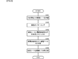
- FIG. 5 is a flowchart showing a manufacturing process of the resin substrate according to the embodiment of the present invention.
- 6 (A) and 6 (B) are exploded cross-sectional views illustrating the shape of the resin substrate according to the embodiment of the present invention during manufacture.
- a single-sided copper-attached resin sheet is prepared for a laminate of resin substrates 10 (S101).
- the resin sheet is made of a thermoplastic resin.
- the copper foil is patterned using a photolithography method or the like (S102). 6A, the conductor pattern 210 is formed on the resin sheets 101, 102, 103, the conductor pattern 220 is formed on the resin sheets 104, 105, and the external connection conductors 201, 202 are resin sheets. 106.
- a hole is formed in the resin sheet using a laser or the like (S103). 6B, interlayer connection holes V310 are formed in the resin sheets 101, 102, and 103, and interlayer connection holes V320 are formed in the resin sheets 104, 105, and 106. At this time, the diameter ⁇ 10 of the hole V310 is larger than the diameter ⁇ 20 of the hole V320.
- the conductive paste is filled into the holes V310 and V320 for interlayer connection (S104).
- the conductive paste is, for example, a mixture of Sn metal powder as a main component, one or more metals or alloys selected from Cu, Ni, Ag, and Mo as an auxiliary component, and an organic solvent.
- the resin sheets 101-106 are laminated and thermocompression bonded (S105). By this heating, the resin sheets 101-106 are bonded. Further, the conductive pace is solidified, and the interlayer connection conductors 310 and 320 are formed. Thereby, the resin substrate 10 is formed.
- the manufacturing method of the present embodiment it is possible to easily manufacture the resin substrate 10 capable of suppressing warpage due to thermal history.
- the resin sheet is not limited to thermoplasticity.
- a resin substrate can be formed without any other material such as an adhesive between the resin sheets. Thereby, the curvature by the difference of a deformation
- the first portion P01 includes three resin sheets, and the second portion P02 includes two resin sheets.
- each of the first part P01 and the second part P02 only needs to include at least one resin sheet.
- the number of resin sheets in the first part P01 and the second part P02 may not be equal.
- a resin substrate having a planar conductor pattern formed on all resin sheets has been described.
- the planar conductor pattern may not be formed.
- the interlayer connection conductor may not be formed.
- one of the first part and the second part may not include a planar conductor pattern at all.
- Resin substrate 11 Front surface 12: Back surface 90: Printed wiring board 100: Main body 101, 102, 103, 104, 105, 106: Resin sheet 201, 202: External connection conductor 210, 220: Conductor pattern 310, 320: Interlayer Connection conductors 901, 902: Land conductor P01: First part P02: Second part V310, V320: Hole
Landscapes
- Engineering & Computer Science (AREA)
- Microelectronics & Electronic Packaging (AREA)
- Manufacturing & Machinery (AREA)
- Chemical & Material Sciences (AREA)
- Dispersion Chemistry (AREA)
- Production Of Multi-Layered Print Wiring Board (AREA)
- Structure Of Printed Boards (AREA)
Abstract
樹脂基板(10)は、積層方向の一方端側の樹脂シート(101,102,103)によって構成される第1部分(P01)と、積層方向の他方端側の樹脂シート(104,105,106)によって構成される第2部分(P02)とを備える。複数の樹脂シート(101)-106の厚みは、第1部分(P01)と第2部分(P02)で略同じである。第1部分(P01)の体積に対する第1部分(P01)の平面状の導体パターン(210)の密度は、第2部分(P02)の体積に対する第2部分(P02)の平面状の導体パターン(220)の密度よりも低い。第1部分(P01)に形成される層間接続導体(310)の径φ10の平均は、第2部分(P02)に形成される層間接続導体(320)の径φ20の平均よりも大きい。
Description
本発明は、複数の樹脂シートが積層された樹脂基板に関する。
現在、電子部品には各種の樹脂基板が用いられている。特許文献1の樹脂基板は、複数の樹脂シートを積層してなる。複数の樹脂シートには、導体パターンが形成されている。この構成によって、樹脂基板の複数の層に導体パターンが配置される。
異なる層に配置された導体パターンは、層間接続導体によって接続されている。この構成によって、複数の層の導体パターンは導通している。
従来の樹脂基板は、次に示す課題を有している。図7は、従来の樹脂基板の課題を説明するための側面図である。
樹脂基板10Pは、長尺状の外形を有する平板である。樹脂基板10Pの裏面12には、外部接続導体201,202が形成されている。外部接続導体201は、長さ方向における一方端に形成されている。外部接続導体202は、長さ方向における他方端に形成されている。
この樹脂基板10Pでは、樹脂基板10Pの厚み方向において、表面11側の複数層における導体パターンの密度は、裏面12側の複数層における導体パターンの密度よりも低い。
このような樹脂基板10Pをプリント配線板90に表面実装する場合、外部接続導体201,202を、プリント配線板90のランド導体901,902にそれぞれはんだ400で接合する。しかしながら、表面11側の導体パターンの密度が裏面側の導体パターンの密度よりも低いと、図7に示すように、表面実装のリフロー時の熱履歴等によって、樹脂基板10Pは、表面11側が収縮して反ってしまう。このため、例えば、図7に示すように、外部接続導体201をランド導体901に接合できていても、外部接続導体202をランド導体902に接合できないという実装不良を生じてしまうことがある。特に、図7に示すように、樹脂基板10Pが長尺状であり、長さ方向の両端に外部接続導体201,202が配置されている場合、反りの影響が大きくなり、実装不良がさらに生じ易くなってしまう。
本発明の目的は、熱履歴等による反りを抑制できる樹脂基板を提供することにある。
この発明は、平面状の導体パターンが形成された複数の樹脂シートを備え、該樹脂シートを含む複数の樹脂シートが積層された長尺状の樹脂基板に関し、次の特徴を有する。樹脂基板は、積層方向の他方端よりも一方端側に近い樹脂シートによって構成される第1部分と、複数の樹脂シートにおける積層方向の一方端よりも他方端側に近い樹脂シートによって構成される第2部分と、を備える。第1部分の体積に対する第1部分の導体パターンの密度は、第2部分の体積に対する第2部分の導体パターンの密度よりも低い。第1部分に形成される第1層間接続導体の径の平均は、第2部分に形成される第2層間接続導体の径の平均よりも大きい。
この構成では、樹脂基板の厚み方向に並ぶ第1部分と第2部分と平面状の導体パターンの疎密差が、第1層間接続導体の径の大きさと第2層間接続導体の径の大きさとの差によって軽減される。
また、この発明の樹脂基板では、次の構成であることが好ましい。第1部分の導体パターンおよび第1層間接続導体からなる導体の第1部分の体積に対する密度を基準として、第2部分の導体パターンおよび第2層間接続導体からなる導体の第2部分の体積に対する密度の比は、0.5以上1.0以下である。
この構成では、第1部分と第2部分との密度の差が抑えられ、反りをさらに抑制し易い。
また、この発明の樹脂基板では、複数の樹脂シートは、熱可塑性樹脂であってもよい。この構成では、複数の樹脂シートから樹脂基板が容易に形成される。
また、この発明の樹脂基板は、長手方向に延びる長尺状の外形を有していてもよい。この構成では、本願発明の構成の反りに対する抑制作用がより効果的になる。
この発明によれば、熱履歴等による樹脂基板の反りを抑制することができる。
本発明の実施形態に係る樹脂基板について、図を参照して説明する。図1は、本発明の実施形態に係る樹脂基板の分解断面図である。図2は、本発明の実施形態に係る樹脂基板の断面図である。図3は、本発明の実施形態に係る樹脂基板の外観斜視図である。図4(A)、図4(B)は、本発明の実施形態に係る樹脂基板の層間接続導体の形状を示す拡大断面図である。なお、図1、図2、図4は、樹脂基板の厚みを強調して記載している。
図1、図2、図3に示すように、樹脂基板10は平板である。樹脂基板10の長さ方向の寸法は、幅方向の寸法よりも大幅に長い。言い換えれば、樹脂基板10は長さ方向を長手方向としている。そして、樹脂基板10は長尺状の外形の平板である。なお、本実施形態の構成は、長さ方向が幅方向よりも長く、且つ、長さ方向の寸法が所定値以上である樹脂基板に有効である。例えば、長さ方向の寸法が幅方向の寸法の約2倍以上である場合に、より有効である。
樹脂基板10は、本体100、外部接続導体201,202、導体パターン210,220、層間接続導体310,320を備える。外部接続導体201は、樹脂基板10における長さ方向の一方端に形成されている。外部接続導体202は、樹脂基板10における長さ方向の他方端に形成されている。外部接続導体201,202は、樹脂基板10の裏面12に形成されている。
本体100は、複数の樹脂シート101,102,103,104,105,106(以下、101-106と記載する。)を備える。本体100は、樹脂シート101-106の積層体である。樹脂シート101-106は、略同じ厚みである。樹脂シート101-106は、同じ材料からなり、熱可塑性樹脂からなる。
図1に示すように、樹脂シート101,102,103には、平面状の導体パターン210がそれぞれ形成されている。導体パターン210は、導電性の高い材料、例えば、銅箔からなる。樹脂シート101,102,103には、層間接続導体310がそれぞれ形成されている。層間接続導体310は、本発明の「第1層間接続導体」に相当する。層間接続導体310は、導電ペーストを固化したものである。導電ペーストは、金属粉、有機溶剤等を混練したものであり。樹脂シート101の導体パターン210と樹脂シート102の導体パターン210は、樹脂シート101の層間接続導体310によって接続されている。樹脂シート102の導体パターン210と、樹脂シート103の導体パターン210は、樹脂シート102,103の層間接続導体310によって接続されている。
樹脂シート104,105には、平面状の導体パターン220がそれぞれ形成されている。導体パターン220は、導体パターン210と同様に、導電性の高い材料、例えば、銅箔からなる。樹脂シート105には、層間接続導体320が形成されている。層間接続導体320は、本発明の「第2層間接続導体」に相当する。層間接続導体320は、層間接続導体310と同様に、導電ペーストを固化したものである。樹脂シート104の導体パターン220と樹脂シート105の導体パターン220は、樹脂シート105の層間接続導体320によって接続されている。
樹脂シート106には、外部接続導体201,202が形成されている。外部接続導体201,202は、導体パターン210,220と同様に、導電性の高い材料、例えば、銅箔からなる。樹脂シート106には、層間接続導体330が形成されている。層間接続導体330は、層間接続導体310,320と同様に、導電ペーストを固化したものである。
これらの導体パターン210,220、層間接続導体310,320,330を適宜形成することによって、樹脂基板10に電気回路が構成されている。この電気回路は、一方の入出力端子が外部接続導体201であり、他方の入出力端子が外部接続導体202である。
このような構成において、図1、図2に示すように、樹脂基板10は、積層方向(厚み方向)に沿って、樹脂シート101,102,103からなる第1部分P01と、樹脂シート104,105,106からなる第2部分P02とを備える。第1部分P01は、積層方向の裏面12側の端面よりも表面11側の端面に近い樹脂シートによって構成される部分であり、第2部分P02は、積層方向の表面11側の端面よりも裏面12側の端面に近い樹脂シートによって構成される部分である。すなわち、樹脂基板10において、表面11側(積層方向の一方端側)から裏面12側(積層方向の他方端側)に向かって、第1部分P01、第2部分P02の順に配置されている。
第1部分P01における導体パターン210の密度は、第2部分P02における導体パターン220の密度よりも低い。すなわち、第1部分P01の体積に対する第1部分P01の導体パターン210の密度は、第2部分P02の体積に対する第2部分P02の導体パターン210の密度よりも低い。
一方、図4に示すように、第1部分P01における層間接続導体310の径φ10は、第2部分P02における層間接続導体320の径φ20よりも大きい。すなわち、φ10>φ20の関係にある。なお、ここで、層間接続導体310,320は、図4に示すように、一般的にすり鉢状である。したがって、厚み方向に沿って、層間接続導体310,320の径は変化する。このような場合、層間接続導体310,320の径とは、層間接続導体310,320の厚み方向の中間位置の径を示す。
なお、第1部分P01における全ての層間接続導体310の径を、第2部分P02における全ての層間接続導体320の径よりも大きくしなくてもよい。例えば、第1部分P01における全ての層間接続導体の径が一定でなく、第2部分P02における全ての層間接続導体の径が一定でない場合もある。この場合、第1部分P01における全ての層間接続導体の径の平均値が、第2部分P02における全ての層間接続導体の径の平均値よりも大きければよい。
このような構成とすることによって、第1部分P01における導体(導体パターン210と層間接続導体310)の密度と、第2部分P02における導体(導体パターン220と層間接続導体320)の密度との差が小さくなる。これにより、樹脂基板10の熱履歴による反りを抑制することができる。したがって、表面実装時のリフロー等によって熱が加わった際の樹脂基板10の反りを抑制でき、樹脂基板10をプリント配線板に表面実装する際に、樹脂基板10をプリント配線板に、より確実に実装することができる。
特に、第2部分P02における導体(導体パターン220と層間接続導体320)の密度を基準にして、第1部分P01における導体(導体パターン210と層間接続導体310)の密度は0.5以上1.0以下であると、反りの抑制効果がさらに高まる。
なお、樹脂シートの厚みが異なると、樹脂シートに同じ穴を設けようとしても、厚い樹脂シートの穴は、薄い樹脂シートの穴よりも大きくなる。しかしながら、本発明の第1部分P01の層間接続導体310の径φ10と第2部分P02の層間接続導体320の径φ20との関係は、このような原理によるものでなく、第1部分P01の導体の密度を、第2部分P02の導体の密度に近づけるために、敢えて設定したものである。
このような構成の樹脂基板10は、次に示す工程によって製造される。図5は、本発明の実施形態に係る樹脂基板の製造工程を示すフローチャートである。図6(A)、図6(B)は、本発明の実施形態に係る樹脂基板の製造途中の形状を示す分解断面図である。
まず、片面銅貼りの樹脂シートを、樹脂基板10の積層分用意する(S101)。樹脂シートは、熱可塑性樹脂からなる。
次に、フォトリソ法等を用いて銅箔をパターニングする(S102)。これにより、図6(A)に示すように、導体パターン210が樹脂シート101,102,103に形成され、導体パターン220が樹脂シート104,105に形成され、外部接続導体201,202が樹脂シート106に形成される。
次に、レーザ等を用いて樹脂シートに穴を形成する(S103)。これにより、図6(B)に示すように、層間接続用の穴V310が樹脂シート101,102,103に形成され、層間接続用の穴V320が樹脂シート104,105,106に形成される。この際、穴V310の径φ10は、穴V320の径φ20よりも大きい。
次に、層間接続用の穴V310,V320に、導電ペーストを充填する(S104)。導電ペーストは、例えば、主成分としてSnの金属粉と、副成分としてCu,Ni,Ag,Moから選ばれる1種類以上の金属または合金と、有機溶剤等とを混練したものである。
次に、樹脂シート101-106を積層して、加熱圧着する(S105)。この加熱により、樹脂シート101-106は接着される。また、導電ペースは固化し、層間接続導体310,320が形成される。これにより、樹脂基板10は形成される。
このように、本実施形態の製造方法を用いることによって、熱履歴による反りが抑制可能な樹脂基板10を容易に製造することができる。
なお、樹脂シートは、熱可塑性に限るものではない。しかしながら、熱可塑性の樹脂シートを用いることによって、樹脂シート間に接着材等の他材料を介することなく、樹脂基板を形成できる。これにより、材料間の変形の差による反りをより確実に抑制することができる。
また、上述の説明では、第1部分P01に3枚の樹脂シートを備え、第2部分P02に2枚の樹脂シートを備える態様を示した。しかしながら、第1部分P01と第2部分P02は、それぞれ少なくとも1枚の樹脂シートを備えていればよい。また、第1部分P01と第2部分P02との樹脂シートの枚数は等しくなくてもよい。
また、上述の説明では、全ての樹脂シート(樹脂シート101,102,103,104,105,106)に平面状の導体パターンが形成された樹脂基板について説明したが、一部の樹脂シートにおいては、平面状の導体パターンが形成されていなくてもよい。また、一部の樹脂シートにおいては層間接続導体が形成されなくてもよい。さらには、第1部分および第2部分のいずれか一方においては、平面状の導体パターンを全く含まなくてもよい。
10:樹脂基板
11:表面
12:裏面
90:プリント配線板
100:本体
101,102,103,104,105,106:樹脂シート
201,202:外部接続導体
210,220:導体パターン
310,320:層間接続導体
901,902:ランド導体
P01:第1部分
P02:第2部分
V310,V320:穴
11:表面
12:裏面
90:プリント配線板
100:本体
101,102,103,104,105,106:樹脂シート
201,202:外部接続導体
210,220:導体パターン
310,320:層間接続導体
901,902:ランド導体
P01:第1部分
P02:第2部分
V310,V320:穴
Claims (4)
- 平面状の導体パターンが形成された樹脂シートを備え、該樹脂シートを含む複数の樹脂シートが積層された長手方向を有する樹脂基板であって、
積層方向の他方端よりも一方端側に近い前記樹脂シートによって構成される第1部分と、前記複数の樹脂シートにおける前記積層方向の前記一方端よりも前記他方端側に近い前記樹脂シートによって構成される第2部分と、を備え、
前記第1部分の体積に対する前記第1部分の前記導体パターンの密度は、前記第2部分の体積に対する前記第2部分の前記導体パターンの密度よりも低く、
前記第1部分に形成される第1層間接続導体の径の平均は、前記第2部分に形成される第2層間接続導体の径の平均よりも大きい、
樹脂基板。 - 前記第2部分の体積に対する前記第2部分の前記導体パターンと前記第2層間接続導体の密度を基準とした、前記第1部分の体積に対する前記第1部分の前記導体パターンと前記第1層間接続導体の密度の比は、0.5以上1.0以下である、
請求項1に記載の樹脂基板。 - 前記複数の樹脂シートは、熱可塑性樹脂からなる、
請求項1または請求項2に記載の樹脂基板。 - 前記長手方向に延びる長尺状の外形を有する、請求項1乃至請求項3のいずれかに記載の樹脂基板。
Priority Applications (2)
| Application Number | Priority Date | Filing Date | Title |
|---|---|---|---|
| JP2018503097A JP6547898B2 (ja) | 2016-03-03 | 2017-02-24 | 樹脂基板および電子機器 |
| US16/109,915 US10257923B2 (en) | 2016-03-03 | 2018-08-23 | Resin substrate and electronic device |
Applications Claiming Priority (2)
| Application Number | Priority Date | Filing Date | Title |
|---|---|---|---|
| JP2016-040554 | 2016-03-03 | ||
| JP2016040554 | 2016-03-03 |
Related Child Applications (1)
| Application Number | Title | Priority Date | Filing Date |
|---|---|---|---|
| US16/109,915 Continuation US10257923B2 (en) | 2016-03-03 | 2018-08-23 | Resin substrate and electronic device |
Publications (1)
| Publication Number | Publication Date |
|---|---|
| WO2017150361A1 true WO2017150361A1 (ja) | 2017-09-08 |
Family
ID=59742864
Family Applications (1)
| Application Number | Title | Priority Date | Filing Date |
|---|---|---|---|
| PCT/JP2017/007010 Ceased WO2017150361A1 (ja) | 2016-03-03 | 2017-02-24 | 樹脂基板 |
Country Status (3)
| Country | Link |
|---|---|
| US (1) | US10257923B2 (ja) |
| JP (2) | JP6547898B2 (ja) |
| WO (1) | WO2017150361A1 (ja) |
Families Citing this family (1)
| Publication number | Priority date | Publication date | Assignee | Title |
|---|---|---|---|---|
| JP7006802B2 (ja) * | 2018-09-27 | 2022-01-24 | 株式会社村田製作所 | 樹脂多層基板 |
Citations (3)
| Publication number | Priority date | Publication date | Assignee | Title |
|---|---|---|---|---|
| JP2009152282A (ja) * | 2007-12-19 | 2009-07-09 | Shinko Electric Ind Co Ltd | 集合配線基板及び半導体パッケージ |
| JP2014199948A (ja) * | 2014-06-30 | 2014-10-23 | 株式会社東芝 | 半導体装置およびシステム |
| JP2016018858A (ja) * | 2014-07-07 | 2016-02-01 | 新光電気工業株式会社 | 配線基板、半導体パッケージ |
Family Cites Families (1)
| Publication number | Priority date | Publication date | Assignee | Title |
|---|---|---|---|---|
| JP5660462B2 (ja) | 2011-05-13 | 2015-01-28 | イビデン株式会社 | プリント配線板 |
-
2017
- 2017-02-24 JP JP2018503097A patent/JP6547898B2/ja active Active
- 2017-02-24 WO PCT/JP2017/007010 patent/WO2017150361A1/ja not_active Ceased
-
2018
- 2018-08-23 US US16/109,915 patent/US10257923B2/en active Active
-
2019
- 2019-06-21 JP JP2019115106A patent/JP6885422B2/ja active Active
Patent Citations (3)
| Publication number | Priority date | Publication date | Assignee | Title |
|---|---|---|---|---|
| JP2009152282A (ja) * | 2007-12-19 | 2009-07-09 | Shinko Electric Ind Co Ltd | 集合配線基板及び半導体パッケージ |
| JP2014199948A (ja) * | 2014-06-30 | 2014-10-23 | 株式会社東芝 | 半導体装置およびシステム |
| JP2016018858A (ja) * | 2014-07-07 | 2016-02-01 | 新光電気工業株式会社 | 配線基板、半導体パッケージ |
Also Published As
| Publication number | Publication date |
|---|---|
| JP6547898B2 (ja) | 2019-07-24 |
| US20180368254A1 (en) | 2018-12-20 |
| US10257923B2 (en) | 2019-04-09 |
| JPWO2017150361A1 (ja) | 2018-10-25 |
| JP6885422B2 (ja) | 2021-06-16 |
| JP2019153819A (ja) | 2019-09-12 |
Similar Documents
| Publication | Publication Date | Title |
|---|---|---|
| JP6011573B2 (ja) | 電子部品 | |
| JP6024693B2 (ja) | 電子部品 | |
| US9860978B1 (en) | Rigid-flex board structure | |
| JP5240293B2 (ja) | 回路基板 | |
| JP5684958B1 (ja) | プリント配線基板 | |
| JP5803998B2 (ja) | 電子部品の製造方法及び基板型の端子の製造方法 | |
| JP5803997B2 (ja) | 電子部品の製造方法 | |
| US9743511B1 (en) | Rigid flex circuit board | |
| JP5118238B2 (ja) | 耐食性と歩留まりを向上させたプリント基板 | |
| JP2007142399A (ja) | ペーストバンプを用いた印刷回路基板およびその製造方法 | |
| US20140182899A1 (en) | Rigid-flexible printed circuit board and method for manufacturing same | |
| JP6388097B2 (ja) | 部品内蔵基板の製造方法 | |
| JP6885422B2 (ja) | 樹脂基板および電子機器 | |
| JP2013073989A (ja) | 表面実装型受動素子部品、部品キャリアテープ、部品内蔵配線板 | |
| JP6673304B2 (ja) | 多層基板 | |
| JP2012230954A (ja) | プリント配線板及びプリント配線板の製造方法 | |
| JP2009135285A (ja) | フレキシブルプリント配線板の製造方法およびその方法により製造されたフレキシブルプリント配線板 | |
| JP5293692B2 (ja) | フレックスリジッド配線基板及びその製造方法 | |
| CN107889356B (zh) | 软硬复合线路板 | |
| JP6866229B2 (ja) | リジッド・フレックス多層プリント配線板 | |
| JP5874697B2 (ja) | 多層プリント基板およびその製造方法 | |
| JP2013062441A (ja) | プリント基板及びその製造方法 | |
| TWI760973B (zh) | 超長電路板及其製備方法 | |
| JP2010129878A (ja) | 部品内蔵プリント基板 | |
| WO2013150816A1 (ja) | フレキシブルプリント配線板及びフレキシブルプリント配線板の製造方法 |
Legal Events
| Date | Code | Title | Description |
|---|---|---|---|
| WWE | Wipo information: entry into national phase |
Ref document number: 2018503097 Country of ref document: JP |
|
| NENP | Non-entry into the national phase |
Ref country code: DE |
|
| 121 | Ep: the epo has been informed by wipo that ep was designated in this application |
Ref document number: 17759827 Country of ref document: EP Kind code of ref document: A1 |
|
| 122 | Ep: pct application non-entry in european phase |
Ref document number: 17759827 Country of ref document: EP Kind code of ref document: A1 |